bb_wk1_240_Wastes_Value_Add
批处理数码雨代码解释

批处理数码⾬代码解释做了⼀个批处理的数码⾬,⽼题⽬了主要给新⼿看主要⽤于了解批处理的⼀下知识1.随机变量的使⽤2.变量的叠加下⾯是源代码:复制代码代码如下:@echo offcolor 0a:startset num=0set "echos= ":numset /a a1=%random%%%3if "%a1%" == "1" set "a1= "if "%a1%" == "2" set "a1= "if "%a1%" == "0" set /a a1=%random%%%2set echos=%echos%%a1%set /a num=%num%+1if "%num%" == "75" echo %echos%&&goto :startgoto :num我来详细解释⼀下复制代码代码如下:@echo off::关闭回显(不⽤说了吧)color 0a::这句的意思是改变批处理的字体颜⾊,0a就是颜⾊代码(具体可以看Color命令):startset num=0::定义(重新定义)num的变量,值为0(我们⽤这个变量来计算批处理循环的次数)set "echos= "::定义(重新定义)echos的变量,值为⼀个空格:numset /a a1=%random%%%3::这句就很重要了,这句可以说是整个数码⾬代码的核⼼::这句的意思是定义⼀个随机数,值在"3"以下::要限制随机数的值,必须⽤set命令的/a开关::⽐如我想定义⼀个num的变量,这个变量是随机数,切必须⼩于20,那代码就是::set /a num=%random%%%20::以上是完整的代码,如果没有使⽤/a开关写成了set num=%random%%%20::那么就会出现错误if "%a1%" == "1" set "a1= "::这句意思是如果变量a1(也就是上⼀句的随机变量)值是1的话那么a1的值就是⼀个空格::Ps(这⾥我有必要说⼀下)::我们程序的⽬的是模拟数码⾬::⼤家也许也看过数码⾬,数码⾬不是全是0和1,中间也是有空隙的,这句就是为了达到这个⽬的::下⾯⼀句也是同样的⽬的::最后还有⼀点要提::不知⼤家发现没有我们之前的语句我没有⽤双引号如set num=0::⽽这句 set "a1= " 却⽤了双引号,这是为什么呢::其实,之前的语句set num=0,也可以改为set "num=0"::这样似乎显得⽐较标准,是不是 set "a1= " 也可以改为 set a1= 呢::答案是"No"::因为set a1=这句就算你在语句后⾯加⼊了空格,批处理也不会去识别::导致了a1的值为空,在批处理中,变量的值是不能为空的,所以我们⽤空格代替::就写成 set "a1= "if "%a1%" == "2" set "a1= "::如果a1值为2,那么a1的值就是⼀个空格if "%a1%" == "0" set /a a1=%random%%%2::这句的意思是,如果随机变量a1的值为0,那么a1的值将随机取⼀个2以下的整数::换句话说就是如果a1值是0,那么a1就随机选0和1两个数set "echos=%echos%%a1%"::这⾥就是我所说的变量叠加::之所以⽤引号是因为a1也有可能是空格::其次就是echos=%echos% .. 我们现在只看这段::这句话的意思是定义echos变量为变量echos和变量a1的值::是不是有些晕::我们在程序开始时就把echos变量定为⼀个空格了::所以这次定义就吧echos定义为⼀个空格+变量a1::是不是清晰了点?::我们⽤实例来吧::变量echos现在是⼀个空格我们⽤[空格]代替::我们再假设变量a1是数字1::那么这次变量就是把 echos定义为 [空格]+1::所以语句执⾏后echos 的值就是⼀个空格然后是数字1::对吧...清晰了吧?这句其实就是变量叠加::如果语句继续执⾏,那么echos 的值是 "[空格]1" 吧?::然后程序再次执⾏a1的值假设是数字2::那么set "echos=%echos%%a1%"的意思就是::定义变量echos的值为 "[空格]1" + 数字2,也就是 "[空格]12" ::.....set /a num=%num%+1::这句意思是变量num的值加⼀(也就是循环了⼀次)if "%num%" == "75" echo %echos%&&goto :start::当循环执⾏以上语句了75次后显⽰⼀次叠加的变量echos::换句话说就是循环以上语句75次后显⽰变量echosgoto :num::跳转到标签num附Color命令各类颜⾊代码。
Cia DS301 appendix V0.2-Electronic Data Sheet Specificationfor CANopen
CAN in Automation e. V.Work Draft:CAN open Electronic Data Sheet Specificationfor CANopenAppendix to CiA Draft Standard 301Revision 0.2Date: 25.10.99HistoryDate ChangesOct 99Initial revision based on Appendix 12 of CiA DS-301 V3.0;Summary of major changes:-clarification and more detailed specification-adjustments to errata sheet and DS-302- denotation- compact storage- module conceptTable of Contents1 Scope...............................................................................................................................1-12 References.......................................................................................................................2-13 Definitions and Abbreviations.........................................................................................3-14 Electronic Data Sheet......................................................................................................4-14.1 Basic Structure........................................................................................................4-24.2 Entry Value Interpretation........................................................................................4-24.3 File Information.......................................................................................................4-34.4 General Device Information.....................................................................................4-44.5 Object Dictionary.....................................................................................................4-54.5.1Mapping of dummy entries...........................................................................4-54.5.2Object Descriptions......................................................................................4-64.5.3Object Links...............................................................................................4-104.5.4Comments..................................................................................................4-105 Device Configuration File DCF.......................................................................................5-125.1 File Information Section........................................................................................5-125.2 Object Sections.....................................................................................................5-125.2.1Parameter Value in standard description...................................................5-125.2.2Denotation.................................................................................................5-135.2.3Compact Storage.......................................................................................5-135.3 Device Commissioning..........................................................................................5-146 Module Concept.............................................................................................................6-156.1 Electronic Data Sheet...........................................................................................6-156.1.1Assignment of extension modules..............................................................6-156.1.2PDOs..........................................................................................................6-156.2 Module Data Sheet................................................................................................6-166.3 Device Configuration File......................................................................................6-176.4 Example................................................................................................................6-18Scope EDS Specification CiA1 ScopeThe usage of devices in a communication network requires configuration of the device parameters and communication facilities. CANopen defines a standardised way to access these parameters via the object dictionary.For handling of the complexity of CANopen systems Software Tools are required. This reduces the complexity of the planning, configuration and analysis process and significantly increases the security of the system.For this purpose Software Tools need an electronic description of the CANopen devices. To allow the usage of manufacturer independent Tools, this document defines a standardised file format Ð called Electronic Data Sheet EDS.Furthermore some derived file formats are specified. The DCF describes a concrete incarnation of a device configuration. The MDS describes modules of devices with a modular structure.References EDS Specification CiA2 References/1/:CiA DS-301, CANopen - Application Layer and Communication Profile, Version 4.0 June 1999/2/:CiA DS-301, CANopen Ð CAL-based Communication Profile for Industrial Systems, Version 3.0 October 1996/3/:CiA DSP-302, Framework for Programmable CANopen Devices, Version 2.0 November 1998/4/:CiA DR-303-4, LSS Ð Layer Setting Services and Protocol, in preparationDefinitions and Abbreviations EDS Specification CiA 3 Definitions and AbbreviationsCAN Controller Area NetworkCiA CAN in Automation international users and manufacturers group e.V.COB Communication Object. (CAN Message) A unit of transportation in a CAN Network. Data must be sent across a Network inside a COB.COB-ID COB-Identifier. Identifies a COB uniquely in a Network. The identifier determines the priority of that COB in the MAC sub-layer too.DCF Device Configuration FileDIN Deutsches Institut fŸr NormungEDS Electronic Data SheetISO International Standardisation OrganisationLSS Layer Settings SpecificationMDS Module Data SheetNMT Network Management. One of the service elements of CANopen Application Layer in the CAN Reference Model. It performs initialisation,configuration and error handling in a CANopen network.OSI Open Systems InterconnectionPDO Process Data ObjectSDO Service Data Object4 Electronic Data SheetIn order to give the user of a CANopen device more support the deviceÕs description should be available in a standardised way. This gives the opportunity to create standardised tools for:·configuration of CANopen devices,·designing networks with CANopen devices,·managing project information on different platforms.Therefore two types of files are introduced to define a CANopen device with electronically means.An EDS can be used to describe the:·Communication functionality and objects as defined in the CANopen Specification DS-301 and Application Frameworks DS-3xx·Device specific objects as defined in the device profiles DS-4XX.The EDS is the template for a device ãXYÒ of the vendor ãUVÒ. The DCF describes the incarnation of a device not only with the objects but also with the values of the objects. Furthermore a value for the baudrate of a device and for the module-id are added.An EDS should be supplied by the vendor of a particular device. If a vendor has no EDS available for his CANopen devices a default EDS might be used. The default EDS comprises all entries of a device profile for a particular device class. The user has to be aware, that the description is different from the concretely implemented features of that device, what might cause severe problems!4.1 Basic StructureThe files are ASCII-coded, the ANSI character set shall be used.The lines can be ended by a LF character or by a CR / LF combination. The total length of a line must not exceed 255 characters.The EDS contains several sections, each of which consists of a group of related entries. The sections and the entries are listed in the following format:[section name]keyname=valueIn this example, [section name] is the name of a section. The enclosing brackets ([]) are required, and the left bracket must be in the leftmost column. Section names are not case sensitive.The keyname=value statement defines the value of each entry. A keyname is the name of an entry. It can consist of any combination of letters and digits, and must be followed immediately by an equal sign (=). The keyname is not case sensitive. If the keyname consists only of digits, it is interpreted as a string, not as a number. This means, that the entry 10=xxx is not the same as 0xA=xxx and 0xA=xxx is not the same as 0x0A=.... The same applies to section names.The value is a string, which can be interpreted depending on the entry (see below). You can include comments and empty lines in EDS files. You must begin each line of a comment with a semicolon (;). It must be in the leftmost column.The sections can appear in any order inside the file. Inside each section, the entries can appear in any order.If not specified otherwise, all sections and entries in this paper are mandatory. In order to support future extensions it is allowed to include additional sections and additional entries inside the sections. Anyhow the Conformance Test Tool will recognise this with warning messages.4.2 Entry Value InterpretationThe interpretation of the values depends on each specific entry. Some general rules are defined:Leading and trailing white space is trimmed. The linekeyname=valueis interpreted the same way askeyname= valueInteger numbers can be written as decimal numbers, hexadecimal numbers or octal numbers. Hexadecimal numbers are preceded by 0x. Octal numbers start with a leading 0 (not followed by x). If the entry contains a number the following lines are identical:keyname=10keyname=0xakeyname=0x0akeyname=0xAkeyname=0x000Akeyname=012If an entry hasnÕt a value, this is denoted by End-Of-Line after the equal sign (empty entry). A missing entry is interpreted the same way as an entry without value.String values are stored without quotes.Octett Strings and raw data of domains are stored as sequence of hexadecimal bytes (without leading 0x). Bytes with a high nibble of 0 must be stored with the leading 0. If the data does not fit within one line, it may be stored in a separate file (refer to chapter 5.2.1).Example for octett string:DemoSeq=01a1053c45aabbccddeeffBitstrings are stored as a sequence of 0 and 1.Example:BitDemo=11001010000111For entries of one of the integer types it is allowed to use a formula. This gives the chance to describe values, that depend on other values. For example, the COB-ID of the default PDOs depend on the Node-ID of the device.The syntax of the formula is given by the following EBNF description:IntEntryValue = $NODEID { Ó+Ó number }For concrete devices, $NODEID will be replaced by the actual Node-ID of the device. The $NODEID must appear at the beginning of the expression. Otherwise the line is interpreted as without a formula. Actually it is only possible to use an offset to this Node-ID in the formula. More complex expressions are not allowed.4.3 File InformationThe EDS contains information about itself. This is useful for version control management. This information is stored in the section [FileInfo].The following keywords are used:FileName file name (according to OS restrictions),FileVersion actual file version (Unsigned8),FileRevision actual file revision (Unsigned8),Description file description (max 255 characters),CreationTime file creation time (characters in format ãhh:mm(AM|PM)Ò), CreationDate date of file creation (characters in format ãmm-dd-yyyyÒ), CreatedBy name or description of file creator (max 255 characters), ModificationTime time of last modification (characters in format ãhh:mm(AM|PM)Ò), ModificationDate date of last file modification (characters in format ãmm-dd-yyyyÒ), ModifiedBy name or description of the modification (max 255 characters). Example:[FileInfo]FileName=vendor1.edsFileVersion=1FileRevision=2Description=EDS for simple I/O-deviceCreationTime=09:45AMCreationDate=05-15-1995CreatedBy=Zaphod BeeblebroxModificationTime=11:30PMModificationDate=08-21-1995ModifiedBy=Zaphod Beeblebrox4.4 General Device InformationThe EDS contains device specific information about· vendor name,· vendor ID,· device name,· device code,· version information,· LSS-information (parts of the LSS-address),· device abilities.This can be found in the section [DeviceInfo].The following keywords are used:VendorNamevendor name (max 255 characters)VendorNumberunique vendor ID according to identity object sub 1(Unsigned32)ProductNameproduct name (max 255 characters)ProductNumberproduct code according to identity object sub 2 (Unsigned32)ProductRevisionproduct revision according to identity object sub 3 (Unsigned32)OrderCodeorder code for this product (max 255 characters)BaudRate_10supported baud rates (Boolean, 0 = not supported, 1 = supported)BaudRate_20BaudRate_50BaudRate_125BaudRate_250BaudRate_500BaudRate_800BaudRate_1000SimpleBootUpMastersimple boot-up master functionality (Boolean, 0 = not supported,1 = supported),SimpleBootUpSlavesimple boot-up slave functionality (Boolean, 0 = not supported,1 = supported),Granularity this value gives you the granularity allowed for the mapping onthis device - most of the existing devices support a granularity of8 (Unsigned8; 0 - mapping not modifiable, 1-64 granularity)DynamicChannelsSupportedaccording to DS-302 this entry describes the facility of dynamicvariable generation. If value is not 0, the additional sectionDynamicChannels exists. Details are given in CiA DS-302 andCiA DS-405.GroupMessaging according to DS-302 this entry describes the facility ofmultiplexed PDOs. (Boolean, 0 = not supported, 1 =supported)Details are given in DS-302.NrOfRXPDO number of Receive PDOs supported.NrOfTXPDO number of Transmit PDOs supported.LSS_Supported support of LSS functionality (Boolean, 0 = not supported, 1 =supported)For compatibility reasons, the entries ProductVersion, LMT_ManufacturerName, LMT_ProductName, ExtendedBootUpMaster and ExtendedBootUpSlave are reserved.Example:[DeviceInfo]VendorName=Nepp Ltd.VendorNumber=156678ProductName=E/A 64ProductNumber=45570ProductRevision=1OrderCode=BUY ME - 177/65/0815LSS_Supported=0BaudRate_50=1BaudRate_250=1BaudRate_500=1BaudRate_1000=1SimpleBootUpSlave=1SimpleBootUpMaster=0NrOfRxPdo=1NrOfTxPdo=24.5 Object DictionaryIn this logical part of the EDS the following information can be found:1. which objects of the object dictionary are supported,2. limit values for parameters,3. default values.4. data types5. additional informationThe description of the objects take place in separate parts corresponding to:· mandatory objects,· optional objects,·manufacturer specific objects.4.5.1 Mapping of dummy entriesSometimes it is required to leave gaps in the mapping of a device. This means that e.g. a device only evaluates the last two data bytes of a PDO of 8 bytes length. The first six bytes should be ignored (perhaps they are evaluated by another device). In this case the mapping of this device must contain dummy entries for these first six bytes.The indices from the data type area of the object dictionary are used for this purpose. The user of a device has to know which data type can be used for creating dummy entries and which not (indeed only the length of the dummy object is important).The section DummyUsage is used for describing dummies. The entries follow this scheme:Dummy<data type index (without 0x-prefix)>={0|1}Example:[DummyUsage]Dummy0001=0Dummy0002=1Dummy0002=1Dummy0003=1Dummy0004=1Dummy0005=1Dummy0006=1Dummy0007=1This means that the device will support the mapping of the data types Integer8/16/32 and Unsigned8/16/32.4.5.2 Object Descriptions4.5.2.1 Object listsThe Object Dictionary is structurally divided into three parts:·Mandatory Objects in [MandatoryObjects] contains only the mandatory objects.These are at least the objects 1000H and 1001H. For devices, that have implemented Version 4.0 of CANopen, additionally the object 1018H.· Optional Objects in [OptionalObjects] contains all other objects of the area 1000H-1FFFH and 6000H-FFFFH.· Manufacturer Specific Objects in [ManufacturerObjects] contains all manufacturer specific objects (located in 2000H-5FFFH).Each of these sections contains a list of the supported objects. Each list contains the entrySupportedObjects - number of entries in the section (Unsigned16)The entries are decimal numbered beginning with number 1. This way the last entry gives the number of available entries.[OptionalObjects]SupportedObjects=101=0x10032=0x10043=0x10054=0x10085=0x10096=0x100A7=0x100C8=0x100D9=0x101010=0x10114.5.2.2 Object descriptionEach of the listed objects has to be described in an own section. The section names are all constructed following the same scheme. The section name is constructed according to[<Index>]using the hexadecimal values for Index and Sub-Index without the leading ã0xÒ and without further leading 0.In a section the following keywords may exist:SubNumber number of sub-indices available at this Index (Unsigned8), notcounting Sub-Index FFH. This allows the description of sub-objects as defined below. This entry is empty or can be missing,if no sub-objects exist.ParameterName parameter name (up to 255 characters)ObjectType This is the object codeDataType This is the Index of the data type of the object in the objectdictionaryLowLimit Lowest limit of object value (only if applicable).HighLimit Upper limit of object value (only if applicable).AccessType Access type for this object (String ãroÒ - read only, ãwoÒ - writeonly, ãrwÒ - read/write, ãrwrÒ - read/write on process input, ãrwwÒ -read/write on process output, ãconstÒ - constant value) DefaultValue default value for this object,PDOMapping Flag, if this object can be mapped into a PDO (Boolean, 0 = notmappable, 1 = mappable).ObjFlags Optional entry for assignment of special behaviour. See below.Objects with object code VAR:HighLimit and LowLimit are optional. DefaultValue is mandatory. SubNumber is not supported.Objects with object code ARRAY or RECORDHighLimit, LowLimit, DefaultValue are not supported. SubNumber is mandatory.DataType, AccessType, PDOMapping are not supported. For exceptions according to compact descriptions refer to chapter 4.5.2.4.Example:[1000]ParameterName=Device TypeObjectType=0x7DataType=0x0007AccessType=roDefaultValue=PDOMapping=0To described a structured object (object has Sub-Indexes) each Sub-Index is described in an own section. The section name is constructed according to the rule[<Index>(sub<Sub-Index>)]using the hexadecimal values for Index and Sub-Index without the leading ã0xÒ and without further leading 0.Example:[1003]SubNumber=2ParameterName=Pre-defined Error FieldObjectType=8[1003sub0]ParameterName=Number of ErrorsObjectType=0x7DataType=0x0005AccessType=roDefaultValue=0x1PDOMapping=0[1003sub1]ParameterName=Standard Error FieldObjectType=0x7DataType=0x0007AccessType=roDefaultValue=0x0PDOMapping=0Application hint:In principle it is possible, that a list of sub-object does not have consecutive Sub-Indexes. The value of Sub-Index 0 always stores the highest Sub-Index implemented. In contrast, the EDS entry SubNumber contains the number of Sub-Index implemented, including the Sub-Index 0.Example:[1010]SubNumber=2ParameterName=Store ParametersObjectType=8[1010sub0]ParameterName=largest Sub-Index supportedObjectType=0x7DataType=0x0005AccessType=roDefaultValue=0x4PDOMapping=0[1010sub4]ParameterName=save manufacturer defined parametersObjectType=0x7DataType=0x0007AccessType=roDefaultValue=0x1PDOMapping=04.5.2.3 Specific FlagsThe entry ObjFlags allows to define a specific behaviour for Tools how to treat an object. Example:A typical task for a configuration software is the Download of a configured DCF file. Doing this without special recognition of special objects leads to the following problem: Objects such as 1010H "Store parameters" will be written with either invalid values or at least in an invalid order. First the objects 1000H up to 100FH are written, then "Store Parameters" and then the other parameters. This will lead to inconsistencies and is not what the user expects. One solution could be the special treatment of such objects by the configuration software. But even then there may happen the case, that device profiles or manufacturer specific objects have a similar problem.These special objects are marked in the EDS and DCF files. The object description sections may contain an entry ObjFlags with an unsigned32 content:The lowest bit is a boolean value (0=false, 1=true) for "Refuse write on Download", the second bit is a boolean value for "Refuse read on Scan", the other bits are reserved for further use by CiA and have to be 0.If the entry is missing, this equals having the value 0. It is recommended to write the entry in the EDS/DCF only if it is not 0. This avoids unnecessary increase of the file size.4.5.2.4 Compact StorageFor devices with many objects and especially many arrays the EDS file might be very big. The load and store process may reach unacceptable times. For this reason the following definitions shall help to store the really necessary information much more compact.Definitions4.5.2.4.1 PDOIn principle the object descriptions for PDOs are all nearly the same. The most important information is the number of TX and RX PDOs which is given by 4.4. It is allowed to leave all PDO object descriptions. To mark this, the boolean entry CompactPDO must be added to the section DeviceInfo:[DeviceInfo]...CompactPDO=1The appropriate data types are implicitly known by the CANopen specifications as well as the default values for the first PDOs COB-Ids. The other values such as TransmissionType and Mapping very often are the goal of Project Planning rsp. Configuration and do not need to be known on load time.If a PDO is described explicitly, all sub-objects of the communication parameters as well as of the mapping parameters of this PDO must be described.Values4.5.2.4.2 ArrayMost often all sections of the Sub-Index es of an array are equal except the name. It is allowed to describe only a template in the main object. For this the additional unsigned8 entry CompactSubObj can be added. If this exists and has a value not equal 0, then·the names are assumed to be xxxn with xxx as the name of the main object and n as the decimal Sub-Index. Sub-Index 0 has the Name NrOfObjects·the object types are assumed to be VAR·the data type for all Sub-Index es except 0 and 255 is given by the entry DataType of the main object. Sub-Index 0 always has the data type Unsigned8.·the limits are assumed to be NONE·the access type for all Sub-Indexes except 0 and 255 is given by the entry AccessType of the main object. The access type for Sub-Index 0 is assumed to be ReadOnly.·the default values for all Sub-Indexes except 0 and 255 is given by the entry DefaultValue of the main object. The default value for Sub-Index 0 is the number given by CompactSubObj· the entry PDOMapping for all Sub-Indexes except 0 and 255 is given by the entry PDOMapping of the main object. Sub-Index 0 is assumed not to be mappable.It must be assumed, that the Sub-Index list does not contain any gaps.If CompactSubObj is used, the entry SubNumber is not supported, it has to be 0 or empty or shall not appear.It is possible to assign explicit names, if the default names are not useful enough. For this a list of according names can appear. The section name is given by [xxxxName] with xxxx as the Index. The entry NrOfEntries gives the number of names in the list. The names are listed with using their Sub-Index as decimal entry name (starting with 1).Example:[2050Name]NrOfEntries=31=NameOfSubIndex12=NameOfSubIndex215=NameOfSubIndex15The names not listed here are built upon the rule given above.Variables4.5.2.4.3 NetworkIn case of Programmable Devices according to CiA DS-302 rsp. CiA DS-405 the description of the dynamic network variable arrays are not written in the EDS. All necessary information is already given by the section DynamicChannels. To ensure a consistent interpretation of the EDS it is not allowed to describe the dynamic network variable sections!Description for Network variables, that are not treated dynamically (DynamicChannelsSupported=0), but are completely described in the EDS, may use the CompactSubObj mechanism.4.5.3 Object LinksIn order to ease the implementation of a configuration tool it is possible to group related objects together via the keyword ObjectLinks.An object link has the following structure:[<index>ObjectLinks]ObjectLinks=<number of available links>1=<index of 1st linked object>2=<index of 2nd linked object>3=<index of 3rd linked object>4=<index of 4th linked object>5=<index of 5th linked object>:The list of object links is numbered decimal beginning with number 1.Example:; assuming we describe closed loop; this is the object ãfactorÒ[5800ObjectLinks]ObjectLinks=0x3; gain1=0x5801; zero2=0x5802; pole3=0x58034.5.4 CommentsComments can be added to the EDS by using the Comments section. This section has only entries determining the line number and the line contents.Lines - number of commentlines (Unsigned16)Line<line number>- one line of comment (max 255 characters). The number is decimal coded.Example:[Comments]Lines=3Line1=|-------------|Line2=| DonÕt panic | Line3=|-------------|5 Device Configuration File DCFThe device configuration file comprises all objects for a configured device. The device configuration file has the same structure as the EDS for this device. There are some additional entries in order to describe the configured device.5.1 File Information SectionLastEDS- file name of the EDS file used as template for this DCF5.2 Object Sections5.2.1 Parameter Value in standard descriptionParameterValue - object value (as defined by ObjectType and DataType) Example:; value for object 1006 (communication cycle period)[1006]SubNumber=0ParameterName=Communication Cycle PeriodObjectType=0x7DataType=0x0007LowLimit=1000HighLimit=100000DefaultValue=20000AccessType=roParameterValue=15000PDOMapping=0If the ObjectType is Domain (0x2) the value of the object can be stored in a file: UploadFile:if a read access is performed for this object, the data are stored in this file (character 255)DownloadFile:if a write access is performed for this object, the data to be written can be taken from this file (character 255)Example:; manufacturer specific object 5600 (downloadable program)[5600]ParameterName=Real Good Program (RGP)ObjectType=0x2DataType=0x000FAccessType=woDownloadFile=C:\FAST\PROGRAMS\FIRST.HEX; manufacturer specific object 5700 (core dump)[5700]ParameterName=Core Dump (CD)ObjectType=0x2DataType=0x000FAccessType=roUploadFile=C:\FAST\DEBUG\DUMPALL.HEX。
bssuggest onsetselectvalue参数
bssuggest onsetselectvalue参数摘要:1.BSSUGGEST 介绍2.ONSETSELECTVALUE 参数的作用3.ONSETSELECTVALUE 参数的使用方法4.ONSETSELECTVALUE 参数的优点5.总结正文:1.BSSUGGEST 介绍BSSUGGEST 是一种基于人工智能的中文分词工具,它可以帮助用户对中文文本进行精确分词。
BSSUGGEST 采用了深度学习技术,其算法基于最新的自然语言处理技术,可以实现高效的中文分词。
2.ONSETSELECTVALUE 参数的作用在BSSUGGEST 中,ONSETSELECTVALUE 是一个重要的参数,它用于控制分词的精确度。
通过设置ONSETSELECTVALUE 参数,用户可以指定分词时需要考虑的最小词语长度。
3.ONSETSELECTVALUE 参数的使用方法在使用BSSUGGEST 时,用户需要在调用函数时设置ONSETSELECTVALUE 参数。
例如,下面的代码展示了如何使用ONSETSELECTVALUE 参数进行分词:```import bssuggesttext = "我爱人工智能助手"result = bssuggest.cut(text, onset_select_value=3)print(result)```在上面的代码中,我们将ONSETSELECTVALUE 参数设置为3,表示我们希望分词时考虑的最小词语长度为3。
4.ONSETSELECTVALUE 参数的优点ONSETSELECTVALUE 参数的优点主要体现在以下几个方面:(1)提高分词精度:通过设置ONSETSELECTVALUE 参数,用户可以控制分词的精确度,从而提高分词结果的准确性。
(2)灵活性高:用户可以根据实际需求调整ONSETSELECTVALUE 参数的值,以获得最佳的分词效果。
(3)易于使用:ONSETSELECTVALUE 参数的使用方法简单,用户只需在调用BSSUGGEST 函数时设置该参数即可。
ANSI-TIA-EIA-568-B.2-1 Cat.6 June 20 2002

PUBLICATIONS or call Global Engineering Documents, USA and Canada (1-800-854-7179) International (303-397-7956)
All rights reserved Printed in U.S.A.
PLEASE! DON'T VIOLATE
This Standard does not purport to address all safety problems associated with its use or all applicable regulatory requirements. It is the responsibility of the user of this Standard to establish appropriate safety and health practices and to determine the applicability of regulatory limitations before its use.
Published by
垃圾回收参数设置标准
垃圾回收参数设置标准垃圾回收是现代软件开发中非常重要的一个环节,它的性能直接影响到系统的稳定性和可靠性。
垃圾回收参数设置标准就是针对不同场景和应用需求,制定的一套最佳的垃圾回收参数配置,以达到系统最佳的性能和稳定性。
本文将从垃圾回收的定义、原理、常见的参数设置以及标准制定等方面进行详细介绍和阐述。
一、垃圾回收的定义和原理垃圾回收是指在程序运行过程中,由垃圾回收器负责自动回收不再被程序使用的内存资源。
在Java、C#等高级编程语言中,垃圾回收是由虚拟机或者运行时环境自动完成的。
在垃圾回收的过程中,会对内存中的对象进行检测,找出哪些对象已经不再被使用,然后回收它们的内存空间,以便进行后续的对象分配和使用。
垃圾回收的原理包括引用计数法、可达性分析法等。
引用计数法是通过统计对象的引用次数来判断对象是否可以被回收,但是由于其无法处理循环引用的情况,因此在实际的系统中较少使用。
可达性分析法则是通过一组根对象(通常是指全局变量和活动栈)来判断对象是否可以被访问到,从而确定其是否可以被回收。
二、垃圾回收参数设置的常见配置在Java虚拟机中,垃圾回收参数的设置非常重要,可以通过参数来调整垃圾回收的执行策略和效果。
常见的垃圾回收参数包括:-Xms、-Xmx、-XX:NewRatio、-XX:SurvivorRatio、-XX:MaxTenuringThreshold、-XX:ParallelGCThreads、-XX:CMSInitiatingOccupancyFraction等。
-Xms和-Xmx是用于设置JVM堆的初始大小和最大大小,-XX:NewRatio和-XX:SurvivorRatio是用于设置新生代和幸存区的比例,-XX:MaxTenuringThreshold是用于设置对象晋升老年代的年龄阈值,-XX:ParallelGCThreads是用于设置并行垃圾回收线程的数量,-XX:CMSInitiatingOccupancyFraction是用于设置CMS垃圾回收器的触发垃圾回收的阈值等。
魔兽世界API_魔兽世界全局函数
魔兽世界API_魔兽世界全局函数魔兽世界API魔兽世界全局函数帐号游戏时间范围函数(Account PlayTime Limit Functions)此类API函数是专门为防沉迷系统而设计的,能计算出当前玩家游戏时间等内容,当前只在亚洲地区有效。
GetBillingTimeRested() - 返回当前帐户已登陆时间。
PartialPlayTime() - 如果用户状态为“疲劳(tired)”则返回1:降低经验及掉落。
NoPlayTime() - 如果用户状态为“不健康的(unhealthy)”则返回1:无经验及掉落。
--------------------------------------------------------------------------------动作函数(Action Functions)这些函数对动作按钮进行操作(通常玩家的动作有可能通过下面列表中的函数执行)。
保护界面 ActionButtonDown(id) - 按下指定动作按钮。
保护界面 ActionButtonUp(id) - 释放指定动作按钮。
ActionHasRange(slot) - 检测指定动作按钮是否受距离限制 (是则返回 1,否则返回 nil) 。
界面BonusActionButtonDown - 触发指定额外动作按钮(宠物或仆从)。
界面 BonusActionButtonUp - 释放指定额外动作按钮 (宠物或仆从)。
保护 CameraOrSelectOrMoveStart() - 在 3D 界面开始 "左键单击" 动作。
(1.10 - 保护)保护 CameraOrSelectOrMoveStop([stickyFlag]) - 在 3D 界面结束 "左键单击" 动作。
(1.10 - 保护)ChangeActionBarPage() - 更改系统动作按钮页面为系统变量CURRENT_ACTIONBAR_PAGE 指定页。
ARM_debug_interface_v5_supplement

2
2.1 2.2 2.3 2.4 2.5 2.6 2.7 2.8 2.9 2.10 2.11 2.12 2.13 2.14 2.15 2.16 2.17
ADIV5.0 ERRATA AND CLARIFICATIONS ........................................................................ 8
Proprietary notice
This ARM Architecture Reference Manual is protected by copyright and the practice or implementation of the information herein may be protected by one or more patents or pending applications. No part of this ARM Architecture Reference Manual may be reproduced in any form by any means without the express prior written permission of ARM. No license, express or implied, by estoppel or otherwise to any intellectual property rights is granted by this ARM Architecture Reference Manual. Your access to the information in this ARM Architecture Reference Manual is conditional upon your acceptance that you will not use or permit others to use the information for the purposes of determining whether implementations of the ARM architecture infringe any third party patents. This ARM Architecture Reference Manual is provided “as is”. ARM makes no representations or warranties, either express or implied, included but not limited to, warranties of merchantability, fitness for a particular purpose, or non-infringement, that the content of this ARM Architecture Reference Manual is suitable for any particular purpose or that any practice or implementation of the contents of the ARM Architecture Reference Manual will not infringe any third party patents, copyrights, trade secrets, or other rights. This ARM Architecture Reference Manual may include technical inaccuracies or typographical errors. To the extent not prohibited by law, in no event will ARM be liable for any damages, including without limitation any direct loss, lost revenue, lost profits or data, special, indirect, consequential, incidental or punitive damages, however caused and regardless of the theory of liability, arising out of or related to any furnishing, practicing, modifying or any use of this ARM Architecture Reference Manual, even if ARM has been advised of the possibility of such damages. Words and logos marked with ® or TM are registered trademarks or trademarks of ARM Limited, except as otherwise stated below in this proprietary notice. Other brands and names mentioned herein may be the trademarks of their respective owners. Copyright © 2009 ARM Limited 110 Fulbourn Road Cambridge, England CB1 9NJ Restricted Rights Legend: Use, duplication or disclosure by the United States Government is subject to the restrictions set forth in DFARS 252.227-7013 (c)(1)(ii) and FAR 52.227-19. This document is Non-Confidential but any disclosure by you is subject to you providing notice to and the acceptance by the recipient of, the conditions set out above.
ST原厂内部指令资料

DIAGNOSTIC COMMANDS Compatible with Drives with >64k CylindersJanuary 13, 2003SERIAL PORT INPUT PARAMETER REPRESENTATIONCommand parameters in this document are represented with single letters, separated by commas.e.g. Sx,y,z - This signifies a serial port command, “S”, that takes in three parameters. Exception: When one parameter is used to input two different values to the command, field width of each parameter will be shown.e.g. Dxxyy – This signifies a serial port command, “D”, that takes in one parameter. Thehigh byte of this parameter (xx) is used to pass one value to the command and the lowbyte (yy) is used to pass a second value to the command.The serial port will accept a max of up to one word (ffffh) for each parameter. For drives with greater than 64k cylinders, the serial port will accept up to a double word (ffff ffffh) for each parameter. S ee the appropriate command description to determine the valid size of a particular parameter.Unless otherwise noted, leading zeros are NOT required.SERIAL PORT OUTPUT DISPLAY REPRESENTATIONOutput display values in this document are represented with either letters or numbers and will show exact field width to aid in the creation and maintenance of serial port parsing software.e.g.When the log is displayed the output to the screen is formatted as shown below.(Log Type 2) (Log Type 4)___x_______Head___x_______Headvv wwww.xxx yyy zz vv wwww.xxx yyy zzwhere wwww is physical cylinder where wwww is physical cylinderLog format for drives with >64k cylinders:(Log Type 2) (Log Type 4)___Head___x_________x_________Headvv wwwww.xxx yyy zz vv wwwww.xxx yyy zzwhere wwwww is physical cylinder where wwwww is physical cylinderor output formatted as follows:Zone0:0006-0B4F800389.020Output format for drives with >64k cylinders:Zone00:0CC84-0DE36884414.1017TABLE OF CONTENTSON-LINE COMMANDS (10)I NTERFACE-S PECIFIC C OMMANDS (10)^E Interface State: Error codes, Max C.H.S, Current transfer mode settings (10)^F Read Segment Record(s) (10)^G Write Queue (10)^I Controller Register Dump (10)^K Niwot RdWr State (10)^Q Resume after ^S (age 50 only) (10)^S Pause intf task and swap to diag monitor (10)^U Currently unused (10)^V Interface Command Echo and Activity Trace Toggle (10)^X Interface and Niwot Command History (10)^Y Display Raw SMART DST Values (for Serial Port running of DST) (10)‘~’Interface Command State (10)G ENERAL C OMMANDS (10)^A Send Certification Code Rev (10)^B(Reserved for Servo Use) (10)^C Firmware Reset (10)^D, ^N Retry Activity Display Toggle. (See Appendix B. for Retry Display Characters.) (10)^L Display Sign-on Message, including firmware version. ** (10)^O, ^]Advance Servo Tracing (10)^P Power Chop enable/disable toggle (11)^Q Cert Display Debug enable/disable toggle ( not age 50 ) (11)^R Restart the Diagnostic Monitor, load overlay from disc (11)^T Restart testing at the current age (11)^W Read/Write statistics gathering enable/disable toggle (11)^Z Restart the Diagnostic Monitor, do not load overlay from disc (11)!Display Current R/W Channel Settings (11)%Show Mux Status. ** (See Appendix B for Description) (11)‘Display Transfer Status (See Appendix B Description) (11).Display Active Status. ** (See Appendix B for Description) (11);Display Machine Status. ** (See Appendix B for Description) (11)<Decrement read/write scope synchronization pulse position (11)>Increment read/write scope synchronization pulse position (11)?Show Buffer Allocation. ** (See Appendix B for Description) (11)^Show Elapsed Time since start of cert test or last ^Z (11)`Show Read/Write Statistics. (See Appendix B for Description) (11){(Reserved for Servo Diagnostic Use) (11)}(Reserved for Servo Diagnostic Use) (11)ESC Interrupt Loop, Batch file or SeaDex script execution (11)COMMON COMMANDS: (AVAILABLE FROM ALL LEVELS EXCEPT LEVEL 8).12 /x Change Level to Diagnostic Monitor Level x (12)CR Loop Break (12)*Special Function for batch file: (12)@x Batch File Label (12)|Batch file terminator (12)+x,y Peek Byte. Display the byte data content of the specified memory address: (12)=x,y,z Poke Byte. Replace the contents of the specified address with the specified data (12)-x,y Peek Word. Display the word contents of the specified address (12)A x,y,z Set Test Space (13)L x,y Loop. Causes the next command to repeat execution, subject to controls specified by x: (13)LEVEL T COMMANDS: CERT PROCESS / TEST (14)A Enable/Disable throttling of drive messaging (14)B x,y Set Baud Rate (14)*** C,,z Reset Certification Test. (available only when overlay is valid) (14)*** D x,y,z Display Cert Logs sequentially from Log x. (available only when overlay is valid) (14)E x,y,z Display/Edit Cert Log(s) (14)F Set Stuff 14*** H x,y,z Display/Reset Health Status Bits. (available only when overlay is valid) (15)*** I,y,z Initialize System Region. (available only when overlay and cert table are valid) (15)J x,y Set Scope Sync from Cert Log entries: (15)K Download Congen file (15)N x,y,z Set Drive Age to x (15)R Read System Sector into System RAM (15)S Check User Slip List for empty or unordered slip list (15)T x Run Factory Test x (15)*** V x,y Display Defect List(s) to screen and add to active log (15)W x,y,z Save System RAM into System Sector (15)Y x,y Set Drive Type (16)a Drive messaging pause toggle switch (16)b,,z Initialize the overlay area of the disc (16)c Write overlays to the disc (16)d x,y,z Download Cert Code (for automated use only) (16)e x,y Download overlay (for automated use only) (16)f Burn new serial flash code that is already downloaded to the buffer and transition to it (16)g x,y,z Call overlay function (16)h Download cert table (for automated use only) (17)*** i x,y,z Initialize/Reset Defect List(s) (available only when overlay is valid) (17)*** j Download SeaDex script (for automated use only) (available only when overlay is valid) (17)k x,y,z Initialize what head to depop (17)*** l x Initialize and write zone buffers in the overlay to RAM (17)*** m,,z Defect Map System Area (available only when overlay is valid) (17)r Reload Cert from Disc and report version number (17)*** s x,y,z Save Defect List(s) (available only when overlay is valid) (17)w x,y Write (Save) Overlay code to Disc (for automated use only) (18)*** x ll,ss,nn Page Log To Host (available only when overlay is valid) (18)#,,z Enter HDA Serial Number (18)$Enter PCBA Serial Number (18)[x,y ASCII Log Control: (18)LEVEL ONE COMMANDS: MEMORY MANIPULATION COMMANDS (19)B x,y Buffer Display (19)D x,y,z Display Memory (19)F Enable Forced Write Bit (19)M Show Flash ROM Information (19)N x,y,z SMART Serial Port Control (19)P Display PCBA Information (19)S x,y,z Edit Memory Byte (20)U x,y,z Edit Buffer Byte (20)*** Y x Converts desired cylinder number to gray code and display the result (20)*** c x,y,z Compare Buffers (available only when overlay is valid) (20)d x Clear overlay code from disc (for automated use only) (20)m x,y,z Edit memory word. Operates same as level 1 ‘S’ command, except operates on words (20)r Read cert code from disc (20)s Send Drive Information (20)t Read cert table from disc (20)u Read SeaDex script from disc (20)*** y x Converts desired gray code to a cylinder number and displays the result (20)LEVEL TWO COMMANDS: NIWOT READ/WRITE COMMANDS (21)B x,y Display Buffer (21)C x,y,z Copy Buffers (21)E x,y,z Display/Edit Cert Log(s) (21)F x,y,z,a Modify Track Defect List (21)G x,y,z,a,b,c MRT Test (available only when overlay is valid) (22)H x Select Head (23)I x,y,z Display/Modify Adaptive Settings (23)J x,y Scope Sync from Log (23)K x,y Set Tracking Offset (23)M x,y,z,w Quick Margin Test (23)N x Adaptive Test for all Heads in Specified Zone (23)O x,y,z Seek-Seek on current head: (23)P x,y,zzww Set Buffer Pattern: (23)Q x,y,,a Write/Read/Read Data (23)R x,y,z,a Read Data (24)S x,y,z Seek Cyl/Head (24)*** T x,y,z Measure Throughput. (available only when overlay is valid) (24)U x,y Spin-Up (25)*** V x,y,z Read/Compare against corresponding write buffer (25)W x,y,z,a Write Data (25)*** X x,y,z Display Data IDs on current track. (available only when overlay is valid) (25)Y x,y,zzaa,b Show/Set Retry Controls (26)Z Spin-Down (26)*** c x,y,z Compare Buffers (available only when overlay is valid) (26)*** d x,y,z,a R e-assign Errors from Log. (available only when overlay is valid) (26)*** e x,y Save Log to Cert Log y. (available only when overlay is valid) (26)*** f x,y,z Wedge Defect Map Current Track(available only when overlay is valid) (26)*** g x,y Slip Servo Wedge (available only when overlay is valid) (27)*** h x Translate Physical sector to Logical sector (27)*** i x,y Show Track Defect List in Active Log (27)*** j,y Read Wedge (27)*** l x Translate Logical sector to Physical sector (27)p x Full Pack Read Or Write (available only when overlay is valid) (28)r x,y,z,a Read Long from current track (28)s x,y,z Seek to Physical Cyl/Head (29)*** t c,hhss,o Translate Physical Cylinder, Servo Sector, Byte offset to LPL (29)u x,y,z Enable display of channel and preamp registers during retry (29)w x Write Long to current track (29)x Show Zone Boundaries and system cylinders as well as the last LBA of the drive (31)y x,z Set Direct Write Mode (31)*** z,y Write Wedge (31)LEVEL THREE COMMANDS: SERVO SEEKING COMMANDS (33)C x,y Acceleration Constant Measurement Test (33)D x,y,z,a,b,c Seek Access Times (33)E x,y,z Display/Edit Certification Test Log(s) (33)*** G x Translate Hex Cylinder to Gray Code (available only when overlay is valid) (33)H x Head Select (33)*** J x Head Switch Offsets (available only when overlay is valid) (33)*** M x,y Actuator Open-loop Move (available only when overlay is valid) (33)O x,y,z Seek-Seek on current head: (33)P x,y,z Position Error Display (33)Q xx,yy Certification Write/Read (34)*** R x,y,z Read Grey Code (available only when overlay is valid) (34)S x,y,z Seek Cyl/Head (34)T Servo Transducer Calibrations (34)U x Spin-Up 34V x,y,z Read GC123 registers (available only when overlay is valid) (34)*** W Read physical Grey Code (available only when overlay is valid) (34)*** Y Hysteresis (available only when overlay is valid) (34)Z Spin-Down (34)*** c Test Air Latch Closed (available only when overlay is valid) (34)*** g x Translate Gray to Hex (available only when overlay is valid) (34)j x,y,z Ramp Test. (Ramp Load drives only – currently Saturn) (35)k Measure Head Position (35)*** m Servo Actuator Geometry Test for MDW (available only when overlay is valid) (35)*** o Test Air Latch Open (available only when overlay is valid) (35)*** p x,y Translate Physical sector to Logical sector. (available only when overlay is valid) (35)*** q x,y Translate Logical sector to Physical sector. (available only when overlay is valid) (35)s x,y,z Seek to Physical Cyl/Head (35)LEVEL FOUR COMMANDS: SERVO TRACKING COMMANDS (36)C xxyy,z,a,b Tracking Test. (available only when overlay is valid) (36)D x,y,z,a,b,c Seek Access Times (36)E x,y,z Display Active Log (36)*** G x Set Tracking/Seek Gain (available only when overlay is valid) (36)H x Select Head x (36)*** I x,y,z Head Stability Test for Heads (default is All Heads) (available only when overlay is valid) (36)K x Servo Offset (37)*** M x,y Actuator Open-loop Move (available only when overlay is valid) (37)N x Napa Servo Adaptive Test for all Heads in Specified Zone (37)O Show MR Head Offset (for current head) (37)P x,y,z Position Error Display for current track (37)S x,y,z Seek Cyl/Head (37)T x,y,z Napa Servo Adaptive Test at the Specified Track (37)*** W Read physical Grey Code (available only when overlay is valid) (37)X x Display 1 rev of servo burst information for current track (37)*** Z x Zap Servo Burst x of the current track. (available only when overlay is valid) (37)*** a Slip error code 90's from the log (available only when overlay is valid) (37)*** c x Track 0 Cal for MDW (available only when overlay is valid) (38)d x Disable/Enable servo from using the ZAP coefficients in the ZAP table (38)*** f Fill Skipped Cylinders (NOT IMPLEMENTED) (available only when overlay is valid) (38)i x Enable/disable ZAP reads (available only when overlay is valid) (38)j,x Adaptive Coherent Feedforward Compensator (ACFC) calibration (MDW only) (38)k Skip MDW serial number cylinders (available only when overlay is valid) (MDW only) (38)l xx Will scan the current position for servo defects and zap the track (38)*** m RRO ZAP System cylinders (available only when overlay is valid) (38)n y,,x Calculate the zap coefficients at the current position (38)p x,y,z Display Spin Error (39)*** q x Change Spin Speed (available only when overlay is valid) (39)r x Reads and displays the specific Track ID contents (39)***s x,y,z Show error count for given log (available only when overlay is valid) (39)t x,y Modifies and views the ZAP RAM table (39)v x,y,z,a ButterFlySeekTest (39)w x Writes the ZAP values in the ZAP RAM table to the Track Ids of the current track (39)x c,,z Skip Cylinder (40)y Show Skipped Cylinders (40)z c,,z Unskip Skipped Cylinder(s) (40)LEVEL SIX COMMANDS: BATCH FILE COMMANDS (41)B x Run Batch File (41)D x List Batch File (41)E x Enter Batch File (41)*Special Function for batch file: (41)@x Batch File Label (41)|Batch file terminator (41)LEVEL SEVEN COMMANDS: READ CHANNEL ADAPTIVE COMMANDS (42)B x,y Display Buffer (42)C x,y,z Copy Buffers (42)D x Display Temperature Diode Values (42)E x,y Display Log(s) (42)F x,y Format Sector/Track (42)G x,y,z Toggle ECC Seed Finder tool (42)H x Select Head x (42)I x,y,z,a Display/Modify Adaptive Settings for the Current Head (42)M x,y,z Napa Single Adaptive Parameter Test (42)N x Napa Data Adaptive Test for all Heads in Specified Zone (43)O h,z, s Read/Write Coarse Offset Calibration (43)P x,y,zzww Set Buffer Pattern: (44)Q x,y Write/Read/Read Data (44)R x,y Read Data (44)S x,y,z Seek Cyl/Head (44)T x,y,z Napa Data Adaptive Test at the Specified Track (44)U x,y Spin-Up (44)V f Set MR Head Read Bias Current for all Heads (44)W x,y Write Data (44)Y x,y,zzaa,b Show/Set Retry Controls (44)Z Spin Down Command (45)a x,y,z MR Bias Backoff (45)b x,y PE and OTC measurements (45)c x,y,z Generate OTC bath tubs by sector (47)d x,y,f Reset Adaptives to the Default Settings (47)e Show diagnostic error counter in the Valiant (DIAGERRCNT) (47)f f Shows the number of TAs/ data retries done (47)g xxxx,yyyy,zz Does Error Rate by sector command (47)i x Issue read / write command (use after p) (47)j Ramp unload without spin-down (Ramp drives only – currently Saturn) (47)n Run the read channel noise calibration at the current track (47)o x,y,z OTC command (48)p Set parameters for Read / Write operation (precedes i command) (48)r Read Adaptives from the System Sectors (48)s xy,z,a Send Byte to Read Channel or Preamp (48)t x,z Get Data from Read Channel or Preamp (48)u Write Unsafe Enable Toggle (48)v,f VCO calibration / display (48)w x,y,z Save System RAM into System Sector (48)x Show Zone Boundaries (49)y x,z Set Direct Write Mode (49)z Toggle Data Randomizer (49)7x,y,z Generate 747 curve (49)9x,y,z Adapt Write Delay (50)LEVEL EIGHT COMMANDS: SERVO TRACK WRITER COMMANDS (53)A Abort any pending servo diagnostic command (53)B Set the read head bias to the serial preamp (53)C x,y,z Execute the servo diagnostic sub commands (53)D Dump Drive Configuration (55)E Lock Spindle Motor (56)F Write Pack-writer Auto Stamp (56)G x Set Spin Gain (56)H x Select head directly (57)I x Push-Inward Actuator (57)J x Spin Speed Adjust (57)K x Added track offset in track follow state (57)Lx Load Head Mask (57)M Increment Head (current head + 1) (57)N Report Logical Spin State (57)O x Message Display (57)P x Push-Out Actuator (57)Q x Read channel (57)R x Read Gray Code (57)S x,y,z Seek Cyl/Head (58)U x Spin-Up Motor (58)Vx Spin-Up 58W x Set Write Current (58)Z Spin-Down (58)c Crash test the Actuator/Crashstops/HDA (58)fx,y Set bank write mode (58)g IMRON signal polarity (58)LEVEL A COMMANDS: NIWOT READ/WRITE LBA COMMANDS(FULLSLIP) (59)C x,y Convert LBA to LPL and display to screen (59)D x,y Convert LBA to PCHS and display to screen (59)E x,y Display Log(s) (59)M x,y Set GrandB Test ports (59)Q,x Write/Read/Read LBA (59)R,x Read LBA Command (59)S x,y,z Seek LBA Command (59)W,x Write LBA Command (59)Y x,y,za Show/Set Retry Controls (59)c x,y,z Convert LPL to LBA and display to screen (59)d x,y,z Convert PCHS to LBA and display to screen (59)l x,y,z Display # of unslipped sectors for LPL to screen (60)LEVEL C COMMANDS: CERT DIAGNOSTIC CTS COMMANDS (61)D Display the Cert Test sequence (61)F vvww,x,yyzz Run Cert CTS Test F with input parameters (61)***P Load Buffers 10-1A with NAPA specific 127 bit pattern, load buffers 1B-1F with 0’s (available only when overlay is valid) (61)***l xxxxx,yPerform Lazy Write / On-Track-Erasure Screen. (available only when overlay is valid) (61)*** p xx,yy Parse Cert Log for Errors by Head (available only when overlay is valid) (62)*** s x,y,z,a CTSSpinUpandDn (available only when overlay is valid) (63)LEVEL D COMMANDS: SEADEX COMMANDS (64)E x,y,z Display SeaDex Log, level-T E-command style (64)I x SeaDex Information tables (64)S x Single Step SeaDex script (64)T x,y,...SeaDex Test Step. (64)b x,y,z Script assembly Breakpoint (65)c x SeaDex Checkpoint (65)l x,y Display SeaDex Log (65)p x Display SeaDex Tune Parameter (65)s x,y Set or Display SeaDex System Variable (65)t x SeaDex Trace Levels (66)v Verify SeaDex Script (66)w x,y,z,a Set or Display SeaDex Word (67)LEVEL E COMMANDS:DRIVE ZONE AND FORMAT COMMANDS (68)a x,y Displays / modifies drive zone parameters. (available only when overlay is valid) (68)b x,y,z Displays / modifies frame format information. (available only when overlay is valid) (69)BOOT CODE DIAGNOSTIC COMMANDS (70)ONLINE COMMANDS, BOOT CODE (70)^D, ^N Retry Activity Display Toggle. ** (See Appendix B. for Retry Display Characters.) (70)^L Display Sign-on Message, including firmware version (70)^O, ^]Advance Servo Tracing (70)^Z Restart the Diagnostic Monitor, do not load overlay from disk (70)!Display Current R/W Channel Settings (70)%Show Mux Status. ** (See Appendix B for Description) (70)‘Display Transfer Status (See Appendix B Description) (70).Display Active Status. ** (See Appendix B for Description) (70);Display Machine Status. ** (See Appendix B for Description) (70)<Decrement read/write scope synchronization pulse position (70)>Increment read/write scope synchronization pulse position (70)LEVEL F COMMANDS:LIMITED BOOT CODE DEBUG SUPPORT (71)+x,y Peek Byte. Display the byte data content of the specified memory address: (71)=x,y,z,w Poke memory. Replace the contents of the specified address with the specified data (71)-x,y Peek Word. Display the word contents of the specified address (71)B x,y Display Buffer (71)C x,y,z Copy Buffers (71)D x,y,z Display Memory (71)P x,y,zzww Set Buffer Pattern: (71)R x Read system sectors information (72)U x Spin-Up 72Z Spin-Down (72)b x,y Set Baud Rate (72)d x,y Download code, used in conjunction with SDLD (72)e x,y,z,w Serial flash access routines (73)r,y,z Reserve tracks read (73)s x Seek to Physical Cyl (FULLSLIP) (73)t x,y,z Write to serial device (73)APPENDIX A: ERROR CODES (74)APPENDIX B: SPECIAL AND RETRY DISPLAY CHARACTERS (75)APPENDIX C: ONLINE COMMAND DISPLAY DESCRIPTIONS (76)S TATISTICS D ISPLAY D ESCRIPTION(`) (76)M UX S TATUS D ISPLAY D ESCRIPTION(%) (78)T RANSFER S TATUS D ISPLAY D ESCRIPTION(‘) (79)A CTIVE S TATUS D ISPLAY D ESCRIPTION(.) (81)M ACHINE S TATUS D ISPLAY D ESCRIPTION(;) (82)B UFFER A LLOCATION D ISPLAY D ESCRIPTION(?) (83)H EALTH B ITS D EFINITIONS: (84)E RROR L OG D ISPLAY (85)Header Format: (85)Defect List Format: (85)ON-LINE COMMANDSThe On-Line commands may be initiated at any time. For the Interface-specific commands, the Interface code must be present in the current memory map for successful execution; the General commands are always avail-able.Interface-Specific CommandsCommand Description(AT)^E Interface State: Error codes, Max C.H.S, Current transfer mode settings^F Read Segment Record(s)Queue^G Write^I Controller Register Dump^K Niwot RdWr State^Q Resume after ^S (age 50 only)^S Pause intf task and swap to diag monitorunused^U Currently^V Interface Command Echo and Activity Trace Toggle^X Interface and Niwot Command History^Y Display Raw SMART DST Values (for Serial Port running of DST)‘~’ Interface Command StateGeneral CommandsCommand Description^A Send Certification Code Rev^B(Reserved for Servo Use)Reset^C Firmware^D, ^N Retry Activity Display Toggle. (See Appendix B. for Retry Display Characters.)^L Display Sign-on Message, including firmware version. **^O, ^] Advance Servo TracingOnline General Commands (Continued)Command Description^P Power Chop enable/disable toggle.^Q Cert Display Debug enable/disable toggle ( not age 50 )^R Restart the Diagnostic Monitor, load overlay from disc.^T Restart testing at the current age.^W Read/Write statistics gathering enable/disable toggle.^Z Restart the Diagnostic Monitor, do not load overlay from disc!Display Current R/W Channel Settings% Show Mux Status. ** (See Appendix B for Description)‘ Display Transfer Status (See Appendix B Description). Display Active Status. ** (See Appendix B for Description); Display Machine Status. ** (See Appendix B for Description)< Decrement read/write scope synchronization pulse position.>Increment read/write scope synchronization pulse position.? Show Buffer Allocation. ** (See Appendix B for Description)^Show Elapsed Time since start of cert test or last ^Z.`Show Read/Write Statistics. (See Appendix B for Description){ (Reserved for Servo Diagnostic Use)} (Reserved for Servo Diagnostic Use)ESC Interrupt Loop, Batch file or SeaDex script execution.** - Standardized and documented in Test Engineering’s Internal Reference Manual, “Microcode Command Set”.COMMON COMMANDS: (Available from All Levels except Level 8) The Common Commands may be executed whenever the diagnostic monitor prompt is present and the monitor is waiting for a command request, except at level 8. The level 8 commands take precedence over the com-mon commands.Command Description/x Change Level to Diagnostic Monitor Level x.Break.CR Loop* Special Function for batch file:*1 Pause batch file execution until input*2,x Delay x milliseconds*3,x Branch to Label x*4,x Increment head and branch to Label x*5 Clear monitor screen*6 Stop on error*7,x Load batch loop counter with x.*8,x Decrement batch loop counter, Branch to Label x if 0.@x Batch File Label.During batch file entry, define this location as Label x.x - Single digit numeric label specification.|Batch file terminatorTerminates the entry of batch files.+x,y Peek Byte. Display the byte data content of the specified memory address:x - upper bits of a greater-than-16 bit addressy - lower 16 bits of a greater-than-16 bit address or the 16 bit address=x,y,z Poke Byte. Replace the contents of the specified address with the specified data.x - upper bits of a greater-than-16 bit addressy - lower 16 bits of a greater-than-16 bit address or the 16 bit addressz - byte data content to be written at the specified address.-x,y Peek Word. Display the word contents of the specified address.x - upper bits of >16 bit addressy - lower 16 bits of >16 bit address or the 16 bit addressCommon Commands (Continued)Command DescriptionA x,y,z Set Test Space x Bit Meanings:Bit # If x = 1 If x = 07 Random Data Existing Buffer Data6 Sequential Out Sequential In5 Odd Cylinders All Cylinders4 Even Cylinders All Cylinders3 (unspecified) (unspecified)2 Random Cylinder/Head Sequential Cylinder/Head1 All Cylinders Current Cylinder0 All Heads Current HeadSpecial ValuesA8,y Set Minimum Cylinder to y >64k cyl compatible* A9,y Set Maximum Cylinder to y >64k cyl compatible* AA,y Set Maximum Head to yAD Set Mins/Maxs to DefaultsA87 Sets random data, random cylinder, random head, all cyls & hds AC7 Randomly select 80% Sequential In, 20% Random addresses IF (Random_Start = TRUEA,,z Select Random start and lengthBit0 set = random start sectorBit1 set = random lengthBit0 set = Display aboveL x,y Loop. Causes the next command to repeat execution, subject to controls specified by x: x Bit Meanings:Bit # If = 1 If = 07 Looping active (internal use) Looping not active (internal use)6 Looping primed (internal use) Looping not primed (internal use)5 Stop on Error Code = y Do Loop Count (y<>0)4 Inhibit Error Message on error Display Error Message on error3 (unspecified) (unspecified)2 Spin Down on Error Remain spinning on error1 Stop on No Error0 Continue on error Stop on errory: Error Code to stop on (if Stop on Error Code is enabled.)Loop Count (default is forever.)* Will accept up to 8 digits for drives with >64k cylindersLEVEL T COMMANDS: Cert Process / TestCommand DescriptionA Enable/Disable throttling of drive messaging.Toggles the state of the drive messaging toggling. Power-up state is throttled - oncebuffer is full, drive messaging system will wait for characters to be transmittedbefore processing further output informationB x,y Set Baud Ratex = 0 Set baud rate to POR default, typically 9600x = 1 Display supported baud rates in the format: =xxxxx > 1 Set supported baud rateTypical baud rates (xxxx leading zeros may be omitted)ratex baud1228 1,228,000921,000921625 625,000460,000460230 230,000115,00011557,60057619,20019296 9,60048 4,80024 2,400y - if entered y contains the delay time in milliseconds. Default isdo not wait for host to return CR, just set new baud rate. If y is enteredthe code will check every millisecond up to y milliseconds for a carriagereturn to be sent back from the host at the new baud rate. If no CR is seen thedrive will default back to 9600 baud.*** C,,z Reset Certification Test. (available only when overlay is valid)Resets health bits and sets age to 1. Clears Scratch Fill Done flag.z - if z = 22h then reset certification test.- if z <> 22 then ignore this command.*** D x,y,z Display Cert Logs sequentially from Log x. (available only when overlay is valid)x - Log to start sequential display; if blank, display only logs of failed tests.y - Displays only log entries with this error codez - Special function:= 40 - Enable fast dump capability for data cataloger capture. Inhibits time delaybetween log dumps and enables fast, unformatted log dump.E x,y,z Display/Edit Cert Log(s)See /2 E for further detail.StuffF SetThe Set Stuff data may be up to 512 characters long. The Set Stuff data format is de-fined by the Seagate-Longmont ATA Vendor Specific Stuff document.。
setupdiopendeviceinfo 示例 -回复

setupdiopendeviceinfo 示例-回复如何使用WDK 中的SetupDiOpenDeviceInfo 函数来获取设备信息。
一、引言在计算机硬件驱动开发领域,了解设备的详细信息对于处理设备冲突、进行驱动更新或替换等操作至关重要。
微软为开发人员提供了Windows 驱动程序开发工具包(Windows Driver Kit,简称WDK),其中包含了一系列用于驱动程序开发的函数和工具。
其中一个重要的函数是SetupDiOpenDeviceInfo,该函数可以帮助开发人员获取设备的详细信息。
二、介绍SetupDiOpenDeviceInfo 函数SetupDiOpenDeviceInfo 函数属于SetupAPI(Windows 打开式设备管理器)函数族,用于打开指定设备的信息以便进行查询或修改。
开发人员可以利用该函数获取设备的硬件ID、厂商ID、设备描述等信息,有助于他们了解设备属性和特性。
三、调用SetupDiOpenDeviceInfo 函数的步骤1. 包含必要的头文件开发人员需要在代码中引入包含SetupDiOpenDeviceInfo 函数声明的头文件。
在C 语言中,可以通过以下代码实现:cinclude <setupapi.h>在C++ 语言中,则需要使用以下代码:cppinclude <setupapi.h>2. 创建一个设备信息集合在调用SetupDiOpenDeviceInfo 函数之前,开发人员必须先创建一个设备信息集合(Device Information Set)。
这个集合将包含所需设备的详细信息。
创建设备信息集合的方法是通过调用SetupDiGetClassDevs 函数,该函数还可以用于搜索指定设备类别的设备。
示例代码如下:cppHDEVINFO hDevInfo;hDevInfo = SetupDiGetClassDevs(NULL, TEXT("USB"), NULL, DIGCF_PRESENT DIGCF_DEVICEINTERFACE);if (hDevInfo == INVALID_HANDLE_VALUE) {获取设备信息集合失败,处理异常情况return;}在以上示例代码中,我们通过指定设备类别为"USB",创建了一个包含USB 设备信息的设备信息集合。
Kenwood TK-941 Conversion 33-centimeter Programmin
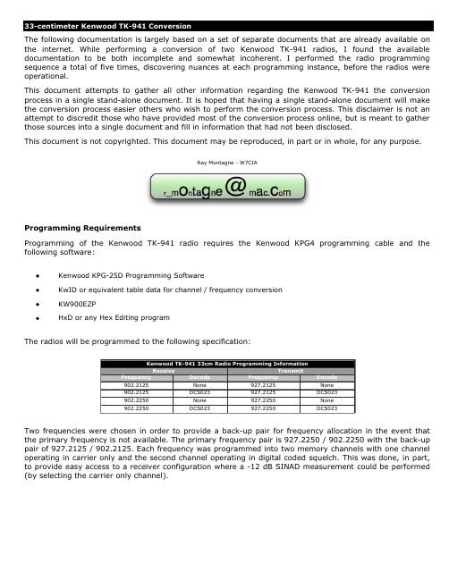
Ray Montagne - W7CIAThe frequency must be converted to a Kenwood Channel Number prior to programming. The following table, obtained from the KW900EZP program documentation by K2MCI, is used to obtain the channel number for the target frequencies:927 902919907920908921909926903 801602403200.00001811612413210.0125 2821622423220.0250 3831632433230.0375 4841642443240.0500 5851652453250.0625 6861662463260.0750 7871672473270.0875 8881682483280.1000 9891692493290.1125 10901702503300.1250 11911712513310.1375 12921722523320.1500 13931732533330.1625 14941742543340.1750 15951752553350.1875 16961762563360.2000 17971772573370.2125 18981782583380.2250 19991792593390.2375 201001802603400.2500 211011812613410.2625 221021822623420.2750 231031832633430.2875 241041842643440.3000 251051852653450.3125 261061862563460.3250 271071872573470.3375 281081882583480.3500 291091892593490.3625 301101902603500.3750 311111912613510.3875 321121922623520.4000 331131932633530.4125 341141942643540.4250 351151952653550.4375 361161962663560.4500 371171972673570.4625 381181982683580.4750 391191992693590.4875 401202002703600.5000 411212012713610.5125 421222022723620.5250 431232032733630.5375 441242042743640.5500 451252052753650.5625 461262062763660.5750 471272072773670.5875 481282082783680.6000 491292092793690.6125927 902919907920908921909926903501302102803700.6250511312112813710.6375521322122823720.6500531332132833730.6625541342142843740.6750551352152853750.6875561362162863760.7000571372172873770.7125581382182883780.7250591392192893790.7375601402202903800.7500611412212913810.7625621422222923820.7750631432232933830.7875641442242943840.8000651452252953850.8125661462262963860.8250671472272973870.8375681482282983880.8500691492292993890.8675701502303003900.8750711512313013910.8875721522323023920.9000731532333033930.9125741542343043940.9250751552353053050.9375761562363063960.9500771572373073970.9625781582383083980.9750791592393093990.9875The target frequency pairs of 927.2125 / 902.2125 and 927.2250 / 902.2250 use FCC channels 17 and 18 respectively.Programming ProcedureI. Launch KPG-25D.exe and start with an empty template by selecting New from the File menu.II. Set the Model to TK-941.III. Select Feature Option from the Edit menu.IV. Set the T.O.T. (Dispatch) parameter to 600. This is the transmission time limit, in dispatch mode, expressed in 15 seconds per step with a range of from 15 seconds to 600 seconds. The default is 60 seconds. These are set to 10 minutes (600 seconds) so that the timers in the repeater controller can be used.V. Set the T.O.T. (Tel)parameter to 600. This is the transmission time limit, in telephone mode, expressed in 15 seconds per step with a range of from 15 seconds to 600 seconds. The default is 180 seconds. These are set to 10 minutes (600 seconds) so that the timers in the repeater controller can be used.VI. Set the Drop out delay time parameter to 1. This sets the time between carrier detect drop out and the resumption of scanning. This parameter can be set from 0 to 254 seconds at 1 second per count. The default is 3 seconds.VII. Set the dwell time parameter to 1. This sets the time between the end of transmission and the resumption of scanning. This parameter can be set from 0 to 254 seconds at 1 second per count. The default is 15 seconds.VIII. Set the Transpond delay time parameter to 3. This sets the delay from the decode of a transpond enabled ID to the beginning of a transpond transmission. This parameter can be set from 0 to 254 seconds at 1 second per count. The default is 3 seconds. If this parameter is set to a value greater than the Drop out delay time then the Drop out delay time will be used as the Transpond delay time.IX. Set the TX inhibit time parameter to 5.0. This parameter sets the period of time that the transmitter is inhibited after an inhibited ID is detected. The value can be set from 0.5 seconds to 8.0 seconds in 0.5 second steps.X. Set the Aux switch parameter to N/A. This parameter toggles the following functions off:A. N/A: No functionB. Option Sig: Option signaling board reset switch.C. Manual Relay: Auxiliary output signal ON/OFF.D. Horn Alert: Horn Alert ON/OFFE. Telephone Search: Automatically searches for a vacant telephone channel (trunked system).F. ALP/Sys.Grp.: Toggle display between alphanumeric or the system & group number.G. Fixed Call: Reset radio to a pre-programmed system & group.H. Del/Add: Provides the user system Delete / Add button.XI. Set the Scan switch parameter to List scan. This parameter sets the scan type selection as follows:A. N/A:Disables the scan switch function and sounds an alert tone (if programmed) when the scan key ispressed.B. List Scan: Automatic roaming scan.C. Fix System Scan: Operator selectable system scan.XII. Set the Revert sys type parameter to Last Use. This parameter sets the programmable transmit destination system & group during scanning. Options include:A. Last Used: Last transmitted system & group.B. Last Called: Last received system & group.XIII. Set the Free System ring back parameter to No. This feature is only active during telephone use (trunked system). The radio will beep when the telephone interconnect line is not busy.XIV. Set the Clear to talk beep parameter to Yes. Upon successful access of a trunked system, this beep tone sounds to alert the user they can begin speaking.XV. Set the System search parameter to None. While a selected system is busy (the radio sounds an intercept tone) then release the PTT key, the radio will start to search for an available system automatically or manually. Options include:A. None: Disable system search.B. Auto: During the intercept tone, keep the PTT key held down and press the SCAN key. Upon release of theSCAN key, system search begins.C. Manual: During the intercept tone, releasing the PTT will initiate auto system search.XVI. Set the Display Character parameter to Grp Name. This parameter selects the display character Group name (Alphanumeric) or System & Group number. If you select the AUX switch as the display character, this selection will be just as default. Options include:A. Sys Grp: Set the display character as System & Group number.B. Grp Name: Set the display character as alphanumeric (pre-programing necessary).XVII. Set the Minimum volume parameter to 0. The minimum volume is the level which will be set automatically every time you turn on the radio. If the volume is adjusted below this level prior to turning the radio off, the volume will be set to this level the next time the radio is turned on. In order to ensure that the speaker is quiet at the repeater site, this value is set to zero. The default value is 8.XVIII. Set the Off hook scan parameter to Disable. The radio is able to scan, even with the mic off hook. Options include:A. Enable: Scan start & stop is independent of the mic hook switch.B. Disable: Mic must be on hook for scanning to start.XIX. Set the Off hook horn alt parameter to Disable. Horn alert is auto disabled when the microphone goes off hook Options include:A. Enable: Off hook auto disable.B. Disable: Manual disable only.XX. Set the Off hook decode parameter to Enable. The radio is still tone squelched, even though the mic is in the off hook condition (valid for QT, DQT and Option Signaling board decode). Options include:A. Enable: Decode signaling active even in the off hook condition.B. Disable: Decode signaling is disabled during off hook.Setting this parameter to Enable allows the radio to operate in decode without having to wire the off-hook signal to the on-hook position.XXI. Set the Access logic sig parameter to Sngl. Pulse. This logic signal is useful for external radio control unit (i.e. Mobile Data Terminal, Computer Aided Dispatch or Over The Air Re-Programming etc) that require a signal at the time of successful trunked repeater access. Options include:A. Continuous: Logic Level high during length of access.B. Sng. Pulse: Logic level high pulse at the time of a successful handshake.XXII. Set the Horn alt logic sig parameter to Pulse. The Horn Alert logic can be used to drive a vehicle horn relay, light or other device. The logic level signal can be set for a continuous (EX: light) or momentary pulse output (EX: vehicle horn relay). Options include:A. Continuous: Continuous logic level low output until reset.B. Pulse: Momentary logic level low output.XXIII.The options should now appear as:XXIV. Layout all of the repeater input frequencies in the first group. Setup each repeater output frequency in a separate system. Using the Kenwood3.exe program, the hexadecimal representation of each frequency can be determined (as seen in the table below).Group & System ConfigurationGroup 1Group 2Group 3Group 4Group 5Group 6Group 7Group 81KC7MCCTX A927.2125CarrierCH. 170xD197KC7MCCTX A927.2125EncodeCH. 170xD197KC7MCCRX A902.2125CarrierCH. 170x0190KC7MCCRX A902.2125EncodeCH. 170x0190KC7MCCTX B927.2250CarrierCH. 180xD297KC7MCCTX B927.2250EncodeCH. 180xD297KC7MCCRX B902.2250CarrierCH. 180x0290KC7MCCRX B902.2250EncodeCH. 180x0290The carrier access groups are not intended for active use but support test configurations, such as performing a -12 dB SINAD measurement on a receiver.XXV. Set the system configuration to Conventional.XXVI. Hit Enter to edit the system configuration.XXVII. Program each group as follows:A. Set the FCC field to 200.B. Set the transmit Encode field as appropriate.C. Set the receive Decode field as appropriate.D. Set the Grp-Name field as appropriate. Use unique text that will help you identify the group name whenusing the HxD program at a later step.E. Set the TlkArnd field to Yes.F. Leave all other fields at their default values.XXVIII. Save the KPG25D configuration file.XXIX. Exit the KPG25D.exe program.XXX. The KPG25D.exe program will have inserted a value of 0x089B, corresponding to channel 200 or 937.5000 MHz, into each of the frequency slots. The channel numbers are stored as a 16-bit word in little endian format. Endian swapping the default channel value results in a value of 0x9B08, which converts to a decimal value of 39688. The decimal channel value can be determined by subtracting the target frequency from 937.5000 MHz and then dividing by the channel frequency step size of 0.0125 MHz. The resulting value is then subtracted from a value of 38923, converted back to hexadecimal and then endian swapped into little endian format before storing the frequency. This is apparently what the Kenwood3.exe program does (except that the conversion to decimal and endian swapping is not required in programming since little endian is the native format for x86 processors).XXXI. Launch the HxD.exe program.XXXII. Open the KPG25D data file with the HxD program.XXXIII. Locate each frequency entry with a value of 0x089B and edit the value to the appropriate value obtained from the Kenwood3.exe program. The Grp-Name field data will be visible in the window and will help to locate the 0x089B value associated with a specific group name..XXXIV. Save the file and exit the Kenwood3.exe program.XXXV. Launch the KPG25D.exe program.XXXVI. Load the KPG25D data file.XXXVII. A view of the Feature option window will show the new channel data.XXXVIII. Program the radio.Filter InstallationTwo TK-941 radios are used to implement the full-duplex link back-bone, with one radio acting as the transmitter and the other radio acting as the receiver. The front-end filter on the receive radio must be swapped out with a filter that has the bandpass frequency having the receive frequency fall within the bandpass.A hot air SMD station was used to remove the pair of filters from the TK-941 receive radio front-end. 915 MHz filters were then installed using a standard soldering station. Note that the filter terminals did not align with the solder pads on the printed circuit board. The terminals had to be bent in to contact the pads prior to soldering. A check was made, using an Ohm meter, to verify that the terminals did not short to the ground traces surrounding the filter terminal pads.Upon completion of the filter installation, the VCO was adjusted to obtain VCO lock.Repeater Controller Interface - Receive RadioThe repeater controller interface requires access to the COS signal and de-emphasized audio. The signal driving the BASE of Q20 presents an Active LOW COS. Further, the COS signal carries only the COS when programmed for COS access or the logical NAND of COS and Tone Decode when programmed for tone or DCS access. The observed logic level on the COS signal shows 3.6 volts when HIGH.Squelch gated de-emphasized audio is available at the junction of C75 and IC6-13. The signal level of the audio, using a 1KHz tone with 3KHz deviation (as used for a -12 dB SINAD measurement), was observed to be 1.2 Vpp.The following annotated PCB view shows where to connect the COS and Gated Audio signals to interface to the repeater controller.The following image shows the repeater controller interface wires attached to the receive radio. The COS wire is blue. The squelch gated de-emphasized audio is orange. A black ground connection is made at emitter of Q20. A Dremel tool was used to grind a small slot to route the cable out of the RF shielded area where the interface signals are available. A Hot Glue gun was used to fasten down the wires, providing strain relief for the PCB pad connections.The power cable chassis strain relief can be lifted, exposing a small but removable plug. Removing this plug allows for routing of the repeater controller interface wires out of the radio chassis.Repeater Controller Interface - Transmit RadioThe transmit radio requires access to the PTT and Microphone input signals. The front panel was removed in preparation to route wires from under the power cable and on to through the chassis to the front panel PCB.The attachment points on the back of the front panel PCB are well marked as follows:1. PTT: Push-to-talk (Green Wire)2. ME: Microphone Return (audio-signal-ground - Black Wire)3. MI: Microphone Input (Red Wire)。
obloader文件拆分的阈值参数

obloader文件拆分的阈值参数obloader是一种用于将大型文件拆分成更小的块的工具,它可以帮助我们更有效地处理大型数据文件。
在使用obloader时,我们需要设置一些参数来控制文件拆分的行为。
其中一个重要的参数是阈值参数。
阈值参数是用来确定何时将文件拆分成更小块的条件。
当文件的大小超过了阈值参数所设定的值时,obloader会自动将文件拆分成更小的块。
这样做的好处是可以提高文件的处理效率,减少内存的占用,并且方便后续的数据处理和分析。
在设置阈值参数时,我们需要考虑到文件的大小和系统的处理能力。
如果阈值参数设置得太小,可能会导致文件被过度拆分,增加了文件的数量和管理的复杂性。
而如果阈值参数设置得太大,可能会导致文件拆分不够细致,影响了后续的数据处理和分析的效果。
一般来说,我们可以根据文件的大小和系统的处理能力来确定阈值参数的值。
如果文件较小,可以适当地增加阈值参数的值,以减少文件的拆分次数。
而如果文件较大,可以适当地减小阈值参数的值,以提高文件的处理效率。
此外,还可以根据文件的特点和需求来设置阈值参数。
例如,如果文件中的数据具有一定的规律性,可以根据规律性来设置阈值参数的值,以便更好地利用数据的特点。
另外,如果文件中的数据需要按照某种方式进行分析,可以根据分析的需求来设置阈值参数的值,以便更好地满足分析的要求。
总之,obloader文件拆分的阈值参数是一个重要的设置,它可以影响到文件的处理效率和后续数据处理的效果。
在设置阈值参数时,我们需要考虑到文件的大小、系统的处理能力、文件的特点和需求等因素。
通过合理地设置阈值参数,我们可以更好地利用obloader工具,提高文件的处理效率,并且方便后续的数据处理和分析。
SIMATIC Energy Manager PRO V7.2 - Operation Operat

2 Energy Manager PRO Client................................................................................................................. 19
2.1 2.1.1 2.1.2 2.1.3 2.1.4 2.1.5 2.1.5.1 2.1.5.2 2.1.6
Basics ................................................................................................................................ 19 Start Energy Manager ........................................................................................................ 19 Client as navigation tool..................................................................................................... 23 Basic configuration ............................................................................................................ 25 Search for object................................................................................................................ 31 Quicklinks.......................................................................................................................... 33 Create Quicklinks ............................................................................................................... 33 Editing Quicklinks .............................................................................................................. 35 Help .................................................................................................................................. 38
MORNSUN B05_XT-2WR3 Series DC DC Converter Datashe

2W isolated DC-DC converterFixed input voltage,unregulated single outputPatent Protection RoHSFEATURES●Continuous short-circuit protection ●No-load input current as low as 8mA●Operating ambient temperature range:-40℃to+105℃●High efficiency up to 86%●Compact SMD package●I/O isolation test voltage 1.5k VDC●Industry standard pin-outB05_XT-2WR3series are designed for use in distributed power supply systems and especially suitable in applications such as pure digital circuits,low frequency analog circuits,relay-driven circuits and data switching circuits.Selection GuideCertificationPart No.Input Voltage (VDC)OutputFull Load Efficiency (%)Min./Typ.Capacitive Load(µF)Max.Nominal (Range)Voltage (VDC)Current(mA)Max./Min.--B0503XT-2WR35(4.5-5.5) 3.3400/4074/782400B0505XT-2WR35400/4080/842400B05X7XT-2WR37286/2980/841000B0509XT-2WR39222/2281/851000B0512XT-2WR312167/1781/85560B0515XT-2WR315133/1382/86560B0524XT-2WR32483/882/86220Input SpecificationsItemOperating ConditionsMin.Typ.Max.UnitInput Current(full load /no-load)5VDC input3.3VDC output--339/8357/--mA5VDC/7VDC output --477/8500/--9VDC/12VDC output --471/8494/--15VDC/24VDC output--466/8488/--Reflected Ripple Current*--15--Surge Voltage (1sec.max.)-0.7--9VDCInput Filter Capacitance filter Hot PlugUnavailableNote:*Reflected ripple current testing method please refer to DC-DC Converter Application Note for specific operation.Output SpecificationsItemOperating ConditionsMin.Typ.Max.UnitVoltage AccuracySee output regulation curve (Fig.1)Linear RegulationInput voltage change:±1%3.3VDC output----±1.5--5VDC/7VDC/9VDC/12V DC/15VDC/24VDC output ----±1.2Load Regulation10%-100%load3.3VDC output --1020%5VDC/7VDC output--9159VDC output--81012VDC/15VDC output --71024VDC output--610Ripple &Noise*20MHz bandwidth --75200mVp-p Temperature Coefficient Full load--±0.02--%/℃Short-circuit ProtectionContinuous,self-recoveryNote:*The“parallel cable”method is used for ripple and noise test,please refer to DC-DC Converter Application Notes for specific information. General SpecificationsItem Operating Conditions Min.Typ.Max.UnitIsolation Input-output electric strength test for1minute with aleakage current of1mA max.1500----VDC Insulation Resistance Input-output resistance at500VDC1000----MΩIsolation Capacitance Input-output capacitance at100kHz/0.1V--20--pFOperating Temperature Derating when operating temperature≥85℃,(seeFig.2)-40--105℃Storage Temperature-55--125Case Temperature Rise Ta=25℃--25--Storage Humidity Non-condensing5--95%RHReflow Soldering Temperature*Peak temp.Tc≤245℃,maximum durationtime≤60s over217℃Vibration10-150Hz,5G,0.75mm.along X,Y and Z Switching Frequency Full load,nominal input voltage--220--kHz MTBF MIL-HDBK-217F@25℃3500----k hours Moisture Sensitivity Level(MSL)IPC/JEDEC J-STD-020D.1Level1Note:*See also IPC/JEDEC J-STD-020D.1.Mechanical SpecificationsCase Material Black plastic;flame-retardant and heat-resistant(UL94V-0)Dimensions13.20x11.40x7.25mmWeight 1.4g(Typ.)Cooling Method Free air convectionElectromagnetic Compatibility(EMC)Emissions CE CISPR32/EN55032CLASS B(see Fig.4for recommended circuit) RE CISPR32/EN55032CLASS B(see Fig.4for recommended circuit)Immunity ESD IEC/EN61000-4-2Air±8kV,Contact±6kV perf.Criteria B Typical Characteristic Curves3.3VDC output5VDC/7VDC/9VDC/12VDC/15VDC/24VDC outputFig.1Design Reference1.Typical applicationInput and/or output ripple can be further reduced,by connecting a filter capacitor from the input and/or output terminals to ground as shown in Fig.3.Choosing suitable filter capacitor values is very important for a smooth operation of the modules,particularly to avoid start-up problems caused by capacitor values that are too high.For recommended input and output capacitor values refer to Table 1.Vin0VDCCinDC CoutFig.3Table 1:Recommended input and output capacitor valuesVin Cin Vo Cout5VDC 4.7µF/16V3.3VDC/5VDC 10µF/16V ----7VDC/9VDC4.7µF/16V ----12VDC 2.2µF/25V ----15VDC 1µF/25V ----24VDC0.47µF/50V2.EMC compliance circuitFig.4EmissionsC1,C24.7µF /16VC3Refer to the Cout in Fig.3CY 270pF/2kV LDM6.8µH3.For additional information,please refer to DC-DC converter application notes on80O u t p u t P o w e r P e r c e n t (%)Ambient Temp.()℃Temperature Derating CurveSafe Operating AreaFig.2Dimensions and Recommended Layout Tape and Reel InfoNotes:1.For additional information on Product Packaging please refer to .Tube Packaging bag number:58210024,RollPackaging bag number:58200054;2.If the product is not operated within the required load range,the product performance cannot be guaranteed to comply with allparameters in the datasheet;3.The maximum capacitive load offered were tested at input voltage range and full load;4.Unless otherwise specified,parameters in this datasheet were measured under the conditions of Ta=25℃,humidity<75%RH with nominalinput voltage and rated output load;5.All index testing methods in this datasheet are based on our company corporate standards;6.We can provide product customization service,please contact our technicians directly for specific information;7.Products are related to laws and regulations:see"Features"and"EMC";8.Our products shall be classified according to ISO14001and related environmental laws and regulations,and shall be handled byqualified units.MORNSUN Guangzhou Science&Technology Co.,Ltd.Address:No.5,Kehui St.1,Kehui Development Center,Science Ave.,Guangzhou Science City,Huangpu District,Guangzhou,P.R.China Tel:86-20-38601850Fax:86-20-38601272E-mail:***************。
MLX90614 C代码
//This is need if
Request Command is sent even when the module is in SMBus
mode
delay(DEL200ms);
//Wait after
POR,Tvalid=0.15s
while(1)
{
data=MemRead(SlaveAddress,command); //Read memory
#pragma interruptlow low_isr void low_isr(void) { // User code... }
#pragma code
//********************************************************
*********************************************************
//********************************************************
*********************************************************
#pragma config OSC=HS,FSCM=OFF,IESO=ON
//
HEADER FILES
//********************************************************
*********************************************************
#include <p18F4320.h>
//
Fosc=11.0592MHz, Tcy=362ns
addbindvalue用法 -回复

addbindvalue用法-回复AddbindValue是一个在编程中常用的方法,它可以用于向数据库查询中添加参数绑定值。
在本文中,我们将介绍AddbindValue的用法,并逐步回答与其相关的问题。
第一步:什么是AddbindValue?AddbindValue是一种数据库查询方法,它可以将查询参数绑定值添加到查询语句中。
它在编程中非常有用,特别是在处理用户输入或动态生成查询语句时。
通过使用AddbindValue,可以有效地防止SQL注入攻击,并提高数据库查询的效率和安全性。
第二步:如何使用AddbindValue?在使用AddbindValue之前,我们需要连接到数据库并构建一个查询语句。
假设我们有一个名为“users”的表,其中包含“id”和“name”两个字段。
我们想编写一个查询,根据用户输入的ID来查找用户的姓名。
以下是一个示例代码:连接到数据库pdo = new PDO("mysql:host=localhost;dbname=mydatabase", "username", "password");准备查询语句query = "SELECT name FROM users WHERE id = :id"; statement = pdo->prepare(query);绑定参数值id = _POST["id"];statement->bindValue(":id", id);执行查询statement->execute();获取结果result = statement->fetchAll(PDO::FETCH_ASSOC);在上面的代码中,我们首先使用PDO来连接到数据库。
然后,我们准备了一个包含参数占位符的查询语句:“SELECT name FROM users WHERE id = :id”。
cxchecklistbox用法 -回复
cxchecklistbox用法-回复cxchecklistbox是一种方便的工具,用于创建复选框列表,并允许用户选择其中的项目。
它在用户界面设计和数据收集方面非常有用。
本文将逐步介绍cxchecklistbox的用法,帮助您了解如何使用它。
第一步:导入库和创建窗口开始之前,我们需要导入必要的库。
在这种情况下,我们将使用的是Python的Tkinter库。
Pythonfrom tkinter import *接下来,我们可以创建一个可视化窗口,以容纳cxchecklistbox。
Pythonwindow = Tk()window.title("Checklist Box示例")第二步:创建cxchecklistbox接下来,我们将创建并配置cxchecklistbox。
Pythonchecklist_box = ChecklistBox(window, width=50)checklist_box.pack()在这个示例中,我们将cxchecklistbox设置为窗口的宽度为50个字符,并将其放置在窗口中。
第三步:添加项目现在我们可以添加项目到cxchecklistbox中。
Pythonchecklist_box.insert(END, "项目1")checklist_box.insert(END, "项目2")checklist_box.insert(END, "项目3")这将在cxchecklistbox中添加3个项目,分别为“项目1”,“项目2”和“项目3”。
第四步:获取选中的项目cxchecklistbox允许用户选择其中的项目。
我们可以通过以下方式获取用户选择的项目。
Pythonselected_items = [checklist_box.get(i) for i inchecklist_box.curselection()]这将创建一个列表,其中包含用户在cxchecklistbox中选择的项目。
垃圾回收参数设置标准
垃圾回收参数设置标准一、引言垃圾回收是指在计算机程序中自动回收不再被使用的内存空间的过程。
在现代程序设计中,垃圾回收是一个必不可少的环节,它有助于优化内存利用,减少内存泄漏,提高程序性能。
不同的应用场景需要不同的垃圾回收参数设置,不合理的参数设置会对系统性能产生负面影响。
制定一份垃圾回收参数设置标准是非常必要的。
二、垃圾回收算法及原理垃圾回收主要利用的算法包括标记-清除算法、引用计数算法、复制算法和标记-整理算法等。
这些算法原理各不相同,适用于不同的应用场景。
合理选择垃圾回收算法将直接影响程序的性能。
三、垃圾回收参数设置标准1. 根据应用类型设置初始堆大小初始堆大小应该根据不同的应用类型进行设置。
对于内存占用较小的应用,可以设置较小的初始堆大小,减少初始化时的内存占用。
而对于内存占用较大的应用,可以设置较大的初始堆大小,以减少垃圾回收的频率,提高程序性能。
2. 设置最大堆大小最大堆大小应根据系统可用内存进行合理设置。
在不超出系统可用内存的情况下,设置较大的最大堆大小,以减少频繁扩容带来的性能损耗。
3. 设置垃圾回收算法选择合适的垃圾回收算法对系统性能影响巨大。
标记-清除算法适用于大内存应用;引用计数算法适用于小内存应用;复制算法适用于频繁分配和回收对象的应用;标记-整理算法适用于需要优化内存空间布局的应用。
4. 设置垃圾回收频率垃圾回收频率应根据应用的实际情况进行设置。
可以根据内存使用率、对象分配速度和系统负载等因素来动态调整垃圾回收频率,以保证系统在合理的内存占用范围内运行。
5. 考虑并发垃圾回收对于需要保持较高响应速度的应用,可以考虑使用并发垃圾回收。
并发垃圾回收可以在不影响应用线程运行的情况下进行垃圾回收,提高系统的响应速度和并发能力。
6. 调整新生代和老年代比例新生代和老年代的比例直接影响垃圾回收的效率。
可以根据应用的特点和对象的生命周期来动态调整新生代和老年代的比例,以优化垃圾回收效率。
multiple readback operations using getimagedata
multiple readback operations using getimagedata在Web开发中,我们经常需要从图像中获取像素信息,例如在图像编辑器中实现画笔功能,或者在游戏中实现碰撞检测。
为了实现这些功能,我们可以使用Canvas API提供的getimagedata()函数。
它可以从Canvas元素中读取像素数据,并返回一个ImageData对象,该对象包含了每个像素的RGBA值。
在某些情况下,我们可能需要多次读取同一张图片的像素信息。
例如,在实现游戏中的动画效果时,我们需要快速地读取和更新屏幕上的像素信息。
在这种情况下,多次使用getimagedata()函数可能会导致性能问题,因为每次调用都要从内存中读取像素数据。
那么,有没有一种更高效的方法来实现多次读取操作呢?答案是肯定的。
我们可以将像素数据存储在一个数组中,并在需要时直接从该数组中读取数据。
这样,我们就可以避免多次使用getimagedata()函数,从而提高性能。
以下是一个简单的例子:```javascript//获取Canvas元素和上下文var canvas = document.getElementById('myCanvas');var ctx = canvas.getContext('2d');//获取图像像素数据var imageData = ctx.getImageData(0, 0, canvas.width, canvas.height);var data = imageData.data;//将像素数据存储在一个数组中var pixelData = [];for (var i = 0; i < data.length; i += 4) {var r = data[i];var g = data[i + 1];var b = data[i + 2];var a = data[i + 3];pixelData.push([r, g, b, a]);}//读取像素数据var x = 10;var y = 20;var index = (y * canvas.width + x) * 4;var pixel = pixelData[index / 4];console.log(pixel);```在上面的代码中,我们首先使用getimagedata()函数获取图像像素数据,并将其存储在一个数组中。
NV3047datasheet_V0.3
New Vision Microelectronics Inc.August. 2009 Confidential Information Ver.0.3NV3047 Data Sheet480X272 TFT LCD Single Chip Digital DriverPreliminary Version 0.3 August.12.2009Contents1 General Description (3)2 Features (4)3 Block Diagram (5)4 Pad Assignment (6)5 Pad Coordinate (8)6 Pin Description (17)7 Function Description (20)7.1 DC-DC Booster (20)7.2 VCOM Generator (21)7.3 Gate Driver (22)7.4 Source Driver (24)7.5 Gamma adjustment (25)7.6 PWM (33)7.7 TCON (34)7.8 CABC function (37)8 Command Table (39)9 Command Description (40)10 DC Characteristics (49)11 AC Characteristics (50)11.1 SPI interface timing specification (50)11.2 Parallel RGB timing (50)11.3 Serial RGB timing (53)11.4 Power ON/OFF specification (55)12 Application Circuit (58)Revision history (61)New Vision Microelectronics Inc.1 General DescriptionNV3047 is a single chip digital driver for dual-gate TFT LCD panel with maximum 544 channels gate driver outputs and 720 channels source driver outputs, supporting 480RGB*272 or 480RGB*240 resolution.The NV3047 incorporates 8-bit serial and 24-bit parallel RGB interface to receive digital display data. It generates 64-level gamma-corrected gray scale voltages and supports maximum 16M colors display with dithering function. The system function control commands can be set by using 3-wire serial peripheral interface.With advanced design, the NV3047 also incorporates the Contents Adaptive Backlight Control (CABC) function. The backlight brightness can be controlled intelligently depending on image data so that system power dissipation can be greatly reduced with slightest influence on the display quality, making the driver best suitable for small or mid sized portable devices such as cell phones, PDAs, mobile TV devices, etc.New Vision Microelectronics Inc.2 Features¾Support 480RGBx272 or 480RGBx240 graphics display TFT LCD panel¾720 source output and 544 gate output¾64 gray level with 2 bit dithering function to realize 16M colors¾Support 8-bit serial RGB data and 24-bit parallel RGB data input¾3-wire SPI command interface¾Power supply:−VDDIO: 1.8 ~ 3.6V−VCI: 3 ~ 3.6V¾Built in 1.8V LDO for internal logic circuit¾Built in DC-DC converter for gate driver VGH/VGL and panel AC VCOM signal supply ¾Maximum gate driving output range: 30Vp-p¾Source output range: 0.1 ~ VLCD - 0.1¾Source and gate scan direction control¾Programmable gamma correction curve¾Support contrast/brightness adjustment¾Support PAL decimation in 480RGBx240 resolution¾Built-in PWM circuits for LED backlight¾CABC function¾COG packageNew Vision Microelectronics Inc.New Vision Microelectronics Inc.New Vision Microelectronics Inc.4 Pad AssignmentADie Size approximately: 19465 x 72015um2500165011025New Vision Microelectronics Inc.New Vision Microelectronics Inc.New Vision Microelectronics Inc.New Vision Microelectronics Inc.New Vision Microelectronics Inc.New Vision Microelectronics Inc.New Vision Microelectronics Inc.New Vision Microelectronics Inc.New Vision Microelectronics Inc.New Vision Microelectronics Inc.New Vision Microelectronics Inc.New Vision Microelectronics Inc.New Vision Microelectronics Inc.VCIX2 mode, and the 4 booster can be configured to -2x or -1x VCIX2 mode.C1 C1C1C1 Fig 3. VGH/VGL External SettingThe capacitor values are recommended as: C1: 0.1uF ~ 0.33uF, C2: 2.2uF ~ 4.7uF, C3: 2.2uF, C4: 1uF ~New Vision Microelectronics Inc.NV3047—480X272 TFT LCD Single Chip Digital Driver7.2 VCOM Generator©2009The NV3047 can generate COMPP and COMC internally to construct VCOMH and VCOML voltage level. The COMPP and COMC can be programmed by register VDV[4:0] and VCM[4:0]. In addition, the COMPP and COMC can be supplied externally. By this method, the COMPP and COMC can be divided from VGR output level.Fig 4. Vcom BlockNew Vision Microelectronics Inc.Page 21NV3047—480X272 TFT LCD Single Chip Digital Driver7.3 Gate Driver©2009Output BufferLevel ShifterCPV UD STV1 STV2 OEV GON VGHFig 5. Gate DriverBi-directional Shifter Register Input BufferVCCVSSVGLNew Vision Microelectronics Inc.Page 22NV3047—480X272 TFT LCD Single Chip Digital DriverUD=1,normal scanVS©2009HSOEVGONG1G2G3G11UD=0,reverse scanFig 6. Gate SequenceNew Vision Microelectronics Inc.Page 23NV3047—480X272 TFT LCD Single Chip Digital Driver7.4 Source Driver©2009Fig 7. Source BlockFig 8. Source SequenceNew Vision Microelectronics Inc.Page 24NV3047—480X272 TFT LCD Single Chip Digital Driver7.5 Gamma adjustment©2009The NV3047 incorporates gamma adjustment function for the 256-color display. Gamma adjustment is implemented by deciding the 6-grayscale levels with angle adjustment and micro adjustment register. Also, angle adjustment and micro adjustment is fixed for each of the internal positive and negative polarity. Set up by the liquid crystal panel’s specification.Graphics RAM(GRAM) R5 R4 R3R2 R1 R0 G5G4 G3 G2 G1G0 B5 B4 B3 B2 B1B0 Positive polarity RegisterPKP02 PKP01 PKP10 PKP12 PKP11 PKP00 PKP22 PKP21 PRP10 PKP32 PKP31 PKP30 PKP42 PKP41 PKP40 PKP52 PKP51 PKP50 PRP02PRP01 PKP206 64 grayscale Control<R>6 64 grayscale Control<G>6 64 grayscale Control<B>PRP10 PRP12PRP11V0 V1 Grayscale Voltage GeneratorVRP03 VRP02 VRP01 VRP00 VRP14 VRP13 VRP12 VRP11 VRP10LCD DriverLCD DriverLCD Driver63PKN52 PKN51 PKN50 PKN42 PKN41 PKN40 PKN32 PKN31 PKN30RGLCDBNegative PKN22 PKN21 PKN20 polarity Register PKN12 PKN11 PKN10PKN02 PKN01 PKN00 PRN02 PRN02 PRN00 PRN12 PRN11 PRN10 VRN03 VRN02 VRN01 VRN00 VRN14 VRN13 VRN12 VRN11 VRN10Fig 9. Grayscale Control BlockNew Vision Microelectronics Inc.Page 25NV3047—480X272 TFT LCD Single Chip Digital Driver7.5.1 Structure of Grayscale Amplifier©2009Below figure indicates the structure of the grayscale amplifier. It determines 8 levels(VIN0-VIN7) by the gradient adjuster and the micro adjustment register. Also, dividing these levels with ladder resistors generates GS0 to GS63.Gradient Adjustment register PRP0 PRP1 VLCD 3 3 Micro Adjust Register(6*3bits) PKP0 3 PKP1 3 PKP2 3 PKP3 3 PKP4 3 Amplitude Adjustment register PKP5 VRP0 VRP1 4 5 3VINP0GS08 to 1 selectorVINP18 to 1 selector 8 to 1 selector 8 to 1 selector 8 to 1 selectorVINP2VINP3VINP4VINP58 to 1 selectorVINP6VINP7GS63* Individual ladder resistors are used for positive and negative polarityVGSFig 10. Grayscale AmplifierNew Vision Microelectronics Inc.Page 26NV3047—480X272 TFT LCD Single Chip Digital Driver©2009Fig 11. Resistor Ladder for Gamma Voltages GenerationNew Vision Microelectronics Inc.Page 27NV3047—480X272 TFT LCD Single Chip Digital Driver7.5.2 Gamma Adjustment Register©2009This block is the register to set up the grayscale voltage adjusting to the gamma specification of the LCD panel. This register can independent set up to positive/negative polarities and there are three types of register groups to adjust gradient, amplitude, and micro-adjustment on number of the grayscale, characteristics of the grayscale voltage. (Using the same setting for Reference-value and R.G.B.) Fol owing graphics indicates the operation of each adjusting register.Fig 12. Gamma Adjustment Function 7.5.2.1 Gradient Adjusting Register The gradient-adjusting resistor is to adjust around middle gradient, specification of the grayscale number and the grayscale voltage without changing the dynamic range. To accomplish the adjustment, it controls the variable resistors in the middle of the ladder resistor by registers (PRP(N)0 / PRP(N)1) for the grayscale voltage generator. Also, there is an independent resistor on the positive/negative polarities in order for corresponding to asymmetry drive. 7.5.2.2 Amplitude Adjusting Register The amplitude-adjusting resistor is to adjust amplitude of the grayscale voltage. To accomplish the adjustment, it controls the variable resistors in the boundary of the ladder resistor by registers (VRP(N)0 / VRP(N)1) for the grayscale voltage generator. Also, there is an independent resistor on the positive/negative polarities as well as the gradient-adjusting resistor. 7.5.2.3 Micro Adjusting Register The micro-adjusting register is to make subtle adjustment of the grayscale voltage level. To accomplish the adjustment, it controls each reference voltage level by the 8 to 1 selector towards the 8-level reference voltage generated from the ladder resistor. Also, there is an independent resistor on the positive/negative polarities as wel as other adjusting resistors.New Vision Microelectronics Inc.Page 28NV3047—480X272 TFT LCD Single Chip Digital Driver7.5.3 Ladder Resistor/ 8 to 1 Selector©2009This block outputs the reference voltage of the grayscale voltage. There are two ladder resistors including the variable resistor and the 8 to 1 selector selecting voltage generated by the ladder resistor. The gamma registers control the variable resistors and 8 to 1 selector resistors. Also, there has pin (EXVR) that can be connected to VSS or an external variable resistor for compensating the dispersion of length between one panel to another. Variable Resistor There are 3 types of the variable resistors that are for the gradient and amplitude adjustment. The resistance is set by the resistor (PRP(N)0 / PRP(N)1) and (VRP(N)0/VRP(N)1 as below.VRP(N)0 0000 0001 0010 … 1101 1110 1111 Resistance 0R 2R 4R … 26R 28R 30R VRP(N)1 00000 00001 00010 … 11101 11110 11111 Resistance 0R 1R 2R … 29R 30R 31R PRP(N)[0:1] 000 001 010 011 100 101 110 111 Resistance 0R 4R 8R 12R 16R 20R 24R 28RTable 1. Variable Resistor 8 to 1 Selector In the 8 to 1 selector, a reference voltage VIN can be selected from the levels which are generated by the ladder resistors. There are six types of reference voltage (VIN1 to VIN6) and total y 48 divided voltages can be selected in one ladder resistor. Following figure explains the relationship between the micro adjusting register and the selecting voltage.Positive polarity Register PKP[2:0] 000 001 010 011 100 101 110 111 Selected voltage VINP1 KVP1 KVP2 KVP3 KVP4 KVP5 KVP6 KVP7 KVP8 VINP2 KVP9 KVP10 KVP11 KVP12 KVP13 KVP14 KVP15 KVP16 VINP3 KVP17 KVP18 KVP19 KVP20 KVP21 KVP22 KVP23 KVP24 VINP4 KVP25 KVP26 KVP27 KVP28 KVP29 KVP30 KVP31 KVP32 VINP5 KVP33 KVP34 KVP35 KVP36 KVP37 KVP38 KVP39 KVP40 VINP6 KVP41 KVP42 KVP43 KVP44 KVP45 KVP46 KVP47 KVP48 Register PKP[2:0] 000 001 010 011 100 101 110 111 Negative polarity Selected voltage VINN1 KVN1 KVN2 KVN3 KVN4 KVN5 KVN6 KVN7 KVN8 VINN2 KVN9 KVN10 KVN11 KVN12 KVN13 KVN14 KVN15 KVN16 VINP3 KVN17 KVN18 KVN19 KVN20 KVN21 KVN22 KVN23 KVN24 VINN4 KVN25 KVN26 KVN27 KVN28 KVN29 KVN30 KVN31 KVN32 VINN5 KVN33 KVN34 KVN35 KVN36 KVN37 KVN38 KVN39 KVN40 VINN6 KVN41 KVN42 KVN43 KVN44 KVN45 KVN46 KVN47 KVN48Table 2. PKP and PKNNew Vision Microelectronics Inc.Page 29NV3047—480X272 TFT LCD Single Chip Digital Driver©2009Grayscale voltage V0 V1 V2 V3 V4 V5 V6 V7 V8 V9 V10 V11 V12 V13 V14 V15 V16 V17 V18 V19 V20 V21 V22 V23 V24 V25 V26 V27 V28 V29 V30 V31 V32 V33 V34 V35 V36 V37 V38 V39 V40 V41 V42 V43 V44 V45 V46 V47 V48 V49 V50 V51 V52 V53 V54 V55 V56 V57 V58 V59 V60 V61 V62 V63Positive Polarity VINP0 VINP1 V8+(V1-V8)*(167/222) V8+(V1-V8)*(124/222) V8+(V1-V8)*(90/222) V8+(V1-V8)*(61/222) V8+(V1-V8)*(37/222) V8+(V1-V8)*(17/222) VINP2 V20+(V8-V20)*(108/124) V20+(V8-V20)*(94/124) V20+(V8-V20)*(81/124) V20+(V8-V20)*(70/124) V20+(V8-V20)*(59/124) V20+(V8-V20)*(49/124) V20+(V8-V20)*(39/124) V20+(V8-V20)*(31/124) V20+(V8-V20)*(22/124) V20+(V8-V20)*(15/124) V20+(V8-V20)*(7/124) VINP3 V43+(V20-V43)*(115/122) V43+(V20-V43)*(108/122) V43+(V20-V43)*(102/122) V43+(V20-V43)*(96/122) V43+(V20-V43)*(90/122) V43+(V20-V43)*(84/122) V43+(V20-V43)*(78/122) V43+(V20-V43)*(73/122) V43+(V20-V43)*(68/122) V43+(V20-V43)*(63/122) V43+(V20-V43)*(58/122) V43+(V20-V43)*(53/122) V43+(V20-V43)*(48/122) V43+(V20-V43)*(43/122) V43+(V20-V43)*(38/122) V43+(V20-V43)*(33/122) V43+(V20-V43)*(28/122) V43+(V20-V43)*(24/122) V43+(V20-V43)*(19/122) V43+(V20-V43)*(14/122) V43+(V20-V43)*(9/122) V43+(V20-V43)*(5/122) VINP4 V55+(V43-V55)*(61/65) V55+(V43-V55)*(56/65) V55+(V43-V55)*(51/65) V55+(V43-V55)*(46/65) V55+(V43-V55)*(41/65) V55+(V43-V55)*(35/65) V55+(V43-V55)*(30/65) V55+(V43-V55)*(24/65) V55+(V43-V55)*(19/65) V55+(V43-V55)*(13/65) V55+(V43-V55)*(7/65) VINP5 V62+(V55-V62)*(70/77) V62+(V55-V62)*(62/77) V62+(V55-V62)*(54/77) V62+(V55-V62)*(45/77) V62+(V55-V62)*(33/77) V62+(V55-V62)*(20/77) VINP6 VINP7Negative Polarity VINN7 VINN6 V1+(V8-V1)*(55/222) V1+(V8-V1)*(98/222) V1+(V8-V1)*(132/222) V1+(V8-V1)*(161/222) V1+(V8-V1)*(185/222) V1+(V8-V1)*(205/222) VINN5 V8+(V20-V8)*(16/124) V8+(V20-V8)*(30/124) V8+(V20-V8)*(43/124) V8+(V20-V8)*(54/124) V8+(V20-V8)*(65/124) V8+(V20-V8)*(75/124) V8+(V20-V8)*(85/124) V8+(V20-V8)*(93/124) V8+(V20-V8)*(102/124) V8+(V20-V8)*(109/124) V8+(V20-V8)*(117/124) VINN4 V20+(V43-V20)*(7/122) V20+(V43-V20)*(14/122) V20+(V43-V20)*(20/122) V20+(V43-V20)*(26/122) V20+(V43-V20)*(32/122) V20+(V43-V20)*(38/122) V20+(V43-V20)*(44/122) V20+(V43-V20)*(49/122) V20+(V43-V20)*(54/122) V20+(V43-V20)*(59/122) V20+(V43-V20)*(64/122) V20+(V43-V20)*(69/122) V20+(V43-V20)*(74/122) V20+(V43-V20)*(79/122) V20+(V43-V20)*(84/122) V20+(V43-V20)*(89/122) V20+(V43-V20)*(94/122) V20+(V43-V20)*(98/122) V20+(V43-V20)*(103/122) V20+(V43-V20)*(108/122) V20+(V43-V20)*(113/122) V20+(V43-V20)*(117/122) VINN3 V43+(V55-V43)*(4/65) V43+(V55-V43)*(9/65) V43+(V55-V43)*(14/65) V43+(V55-V43)*(19/65) V43+(V55-V43)*(24/65) V43+(V55-V43)*(30/65) V43+(V55-V43)*(35/65) V43+(V55-V43)*(41/65) V43+(V55-V43)*(46/65) V43+(V55-V43)*(52/65) V43+(V55-V43)*(58/65) VINN2 V55+(V62-V55)*(7/77) V55+(V62-V55)*(15/77) V55+(V62-V55)*(23/77) V55+(V62-V55)*(32/77) V55+(V62-V55)*(44/77) V55+(V62-V55)*(57/77) VINN1 VINN0Table 3. Grayscale Voltage FormulasNew Vision Microelectronics Inc.Page 30NV3047—480X272 TFT LCD Single Chip Digital Driver©2009Reference KVP0 KVP1 KVP2 KVP3 KVP4 KVP5 KVP6 KVP7 KVP8 KVP9 KVP10 KVP11 KVP12 KVP13 KVP14 KVP15 KVP16 KVP17 KVP18 KVP19 KVP20 KVP21 KVP22 KVP23 KVP24 KVP25 KVP26 KVP27 KVP28 KVP29 KVP30 KVP31 KVP32 KVP33 KVP34 KVP35 KVP36 KVP37 KVP38 KVP39 KVP40 KVP41 KVP42 KVP43 KVP44 KVP45 KVP46 KVP47 KVP48 KVP49Formula VLCD63-△V*VRP0/SUMRP VLCD63-△V*(VRP0+8R)/SUMRP VLCD63-△V*(VRP0+12R)/SUMRP VLCD63-△V*(VRP0+16R)/SUMRP VLCD63-△V*(VRP0+20R)/SUMRP VLCD63-△V*(VRP0+24R)/SUMRP VLCD63-△V*(VRP0+28R)/SUMRP VLCD63-△V*(VRP0+32R)/SUMRP VLCD63-△V*(VRP0+36R)/SUMRP VLCD63-△V*(VRP0+36R+VRHP)/SUMRP VLCD63-△V*(VRP0+37R+VRHP)/SUMRP VLCD63-△V*(VRP0+38R+VRHP)/SUMRP VLCD63-△V*(VRP0+39R+VRHP)/SUMRP VLCD63-△V*(VRP0+40R+VRHP)/SUMRP VLCD63-△V*(VRP0+41R+VRHP)/SUMRP VLCD63-△V*(VRP0+42R+VRHP)/SUMRP VLCD63-△V*(VRP0+43R+VRHP)/SUMRP VLCD63-△V*(VRP0+48R+VRHP)/SUMRP VLCD63-△V*(VRP0+49R+VRHP)/SUMRP VLCD63-△V*(VRP0+50R+VRHP)/SUMRP VLCD63-△V*(VRP0+51R+VRHP)/SUMRP VLCD63-△V*(VRP0+52R+VRHP)/SUMRP VLCD63-△V*(VRP0+53R+VRHP)/SUMRP VLCD63-△V*(VRP0+54R+VRHP)/SUMRP VLCD63-△V*(VRP0+55R+VRHP)/SUMRP VLCD63-△V*(VRP0+71R+VRHP)/SUMRP VLCD63-△V*(VRP0+72R+VRHP)/SUMRP VLCD63-△V*(VRP0+73R+VRHP)/SUMRP VLCD63-△V*(VRP0+74R+VRHP)/SUMRP VLCD63-△V*(VRP0+75R+VRHP)/SUMRP VLCD63-△V*(VRP0+76R+VRHP)/SUMRP VLCD63-△V*(VRP0+77R+VRHP)/SUMRP VLCD63-△V*(VRP0+78R+VRHP)/SUMRP VLCD63-△V*(VRP0+90R+VRHP)/SUMRP VLCD63-△V*(VRP0+91R+VRHP)/SUMRP VLCD63-△V*(VRP0+92R+VRHP)/SUMRP VLCD63-△V*(VRP0+93R+VRHP)/SUMRP VLCD63-△V*(VRP0+94R+VRHP)/SUMRP VLCD63-△V*(VRP0+95R+VRHP)/SUMRP VLCD63-△V*(VRP0+96R+VRHP)/SUMRP VLCD63-△V*(VRP0+97R+VRHP)/SUMRP VLCD63-△V*(VRP0+97R+VRHP+VRLP)/SUMRP VLCD63-△V*(VRP0+101R+VRHP+VRLP)/SUMRP VLCD63-△V*(VRP0+105R+VRHP+VRLP)/SUMRP VLCD63-△V*(VRP0+109R+VRHP+VRLP)/SUMRP VLCD63-△V*(VRP0+113R+VRHP+VRLP)/SUMRP VLCD63-△V*(VRP0+117R+VRHP+VRLP)/SUMRP VLCD63-△V*(VRP0+121R+VRHP+VRLP)/SUMRP VLCD63-△V*(VRP0+125R+VRHP+VRLP)/SUMRP VLCD63-△V*(VRP0+127R+VRHP+VRLP)/SUMRPMicro-adjusting register PKP0[2:0]="000" PKP0[2:0]="001" PKP0[2:0]="010" PKP0[2:0]="011" PKP0[2:0]="100" PKP0[2:0]="101" PKP0[2:0]="110" PKP0[2:0]="111" PKP1[2:0]="000" PKP1[2:0]="001" PKP1[2:0]="010" PKP1[2:0]="011" PKP1[2:0]="100" PKP1[2:0]="101" PKP1[2:0]="110" PKP1[2:0]="111" PKP2[2:0]="000" PKP2[2:0]="001" PKP2[2:0]="010" PKP2[2:0]="011" PKP2[2:0]="100" PKP2[2:0]="101" PKP2[2:0]="110" PKP2[2:0]="111" PKP3[2:0]="000" PKP3[2:0]="001" PKP3[2:0]="010" PKP3[2:0]="011" PKP3[2:0]="100" PKP3[2:0]="101" PKP3[2:0]="110" PKP3[2:0]="111" PKP4[2:0]="000" PKP4[2:0]="001" PKP4[2:0]="010" PKP4[2:0]="011" PKP4[2:0]="100" PKP4[2:0]="101" PKP4[2:0]="110" PKP4[2:0]="111" PKP5[2:0]="000" PKP5[2:0]="001" PKP5[2:0]="010" PKP5[2:0]="011" PKP5[2:0]="100" PKP5[2:0]="101" PKP5[2:0]="110" PKP5[2:0]="111" -Reference voltage VINP0VINP1VINP2VINP3VINP4VINP5VINP6VINP7Table 4. Reference Voltages of Positive PolarityNew Vision Microelectronics Inc.Page 31NV3047—480X272 TFT LCD Single Chip Digital Driver©2009Reference KVN0 KVN1 KVN2 KVN3 KVN4 KVN5 KVN6 KVN7 KVN8 KVN9 KVN10 KVN11 KVN12 KVN13 KVN14 KVN15 KVN16 KVN17 KVN18 KVN19 KVN20 KVN21 KVN22 KVN23 KVN24 KVN25 KVN26 KVN27 KVN28 KVN29 KVN30 KVN31 KVN32 KVN33 KVN34 KVN35 KVN36 KVN37 KVN38 KVN39 KVN40 KVN41 KVN42 KVN43 KVN44 KVN45 KVN46 KVN47 KVN48 KVN49Formula VLCD63-△V*VRN0/SUMRN VLCD63-△V*(VRN0+1R)/SUMRN VLCD63-△V*(VRN0+5R)/SUMRN VLCD63-△V*(VRN0+9R)/SUMRN VLCD63-△V*(VRN0+13R)/SUMRN VLCD63-△V*(VRN0+17R)/SUMRN VLCD63-△V*(VRN0+21R)/SUMRN VLCD63-△V*(VRN0+25R)/SUMRN VLCD63-△V*(VRN0+29R)/SUMRN VLCD63-△V*(VRN0+29R+VRHN)/SUMRN VLCD63-△V*(VRN0+30R+VRHN)/SUMRN VLCD63-△V*(VRN0+31R+VRHN)/SUMRN VLCD63-△V*(VRN0+32R+VRHN)/SUMRN VLCD63-△V*(VRN0+33R+VRHN)/SUMRN VLCD63-△V*(VRN0+34R+VRHN)/SUMRN VLCD63-△V*(VRN0+35R+VRHN)/SUMRN VLCD63-△V*(VRN0+36R+VRHN)/SUMRN VLCD63-△V*(VRN0+48R+VRHN)/SUMRN VLCD63-△V*(VRN0+49R+VRHN)/SUMRN VLCD63-△V*(VRN0+50R+VRHN)/SUMRN VLCD63-△V*(VRN0+51R+VRHN)/SUMRN VLCD63-△V*(VRN0+52R+VRHN)/SUMRN VLCD63-△V*(VRN0+53R+VRHN)/SUMRN VLCD63-△V*(VRN0+54R+VRHN)/SUMRN VLCD63-△V*(VRN0+55R+VRHN)/SUMRN VLCD63-△V*(VRN0+71R+VRHN)/SUMRN VLCD63-△V*(VRN0+72R+VRHN)/SUMRN VLCD63-△V*(VRN0+73R+VRHN)/SUMRN VLCD63-△V*(VRN0+74R+VRHN)/SUMRN VLCD63-△V*(VRN0+75R+VRHN)/SUMRN VLCD63-△V*(VRN0+76R+VRHN)/SUMRN VLCD63-△V*(VRN0+77R+VRHN)/SUMRN VLCD63-△V*(VRN0+78R+VRHN)/SUMRN VLCD63-△V*(VRN0+84R+VRHN)/SUMRN VLCD63-△V*(VRN0+85R+VRHN)/SUMRN VLCD63-△V*(VRN0+86R+VRHN)/SUMRN VLCD63-△V*(VRN0+87R+VRHN)/SUMRN VLCD63-△V*(VRN0+88R+VRHN)/SUMRN VLCD63-△V*(VRN0+89R+VRHN)/SUMRN VLCD63-△V*(VRN0+90R+VRHN)/SUMRN VLCD63-△V*(VRN0+91R+VRHN)/SUMRN VLCD63-△V*(VRN0+91R+VRHN+VRLN)/SUMRN VLCD63-△V*(VRN0+95R+VRHN+VRLN)/SUMRN VLCD63-△V*(VRN0+99R+VRHN+VRLN)/SUMRN VLCD63-△V*(VRN0+103R+VRHN+VRLN)/SUMRN VLCD63-△V*(VRN0+107R+VRHN+VRLN)/SUMRN VLCD63-△V*(VRN0+111R+VRHN+VRLN)/SUMRN VLCD63-△V*(VRN0+115R+VRHN+VRLN)/SUMRN VLCD63-△V*(VRN0+119R+VRHN+VRLN)/SUMRN VLCD63-△V*(VRN0+127R+VRHN+VRLN)/SUMRNMicro-adjusting register PKN0[2:0]="000" PKN0[2:0]="001" PKN0[2:0]="010" PKN0[2:0]="011" PKN0[2:0]="100" PKN0[2:0]="101" PKN0[2:0]="110" PKN0[2:0]="111" PKN1[2:0]="000" PKN1[2:0]="001" PKN1[2:0]="010" PKN1[2:0]="011" PKN1[2:0]="100" PKN1[2:0]="101" PKN1[2:0]="110" PKN1[2:0]="111" PKN2[2:0]="000" PKN2[2:0]="001" PKN2[2:0]="010" PKN2[2:0]="011" PKN2[2:0]="100" PKN2[2:0]="101" PKN2[2:0]="110" PKN2[2:0]="111" PKN3[2:0]="000" PKN3[2:0]="001" PKN3[2:0]="010" PKN3[2:0]="011" PKN3[2:0]="100" PKN3[2:0]="101" PKN3[2:0]="110" PKN3[2:0]="111" PKN4[2:0]="000" PKN4[2:0]="001" PKN4[2:0]="010" PKN4[2:0]="011" PKN4[2:0]="100" PKN4[2:0]="101" PKN4[2:0]="110" PKN4[2:0]="111" PKN5[2:0]="000" PKN5[2:0]="001" PKN5[2:0]="010" PKN5[2:0]="011" PKN5[2:0]="100" PKN5[2:0]="101" PKN5[2:0]="110" PKN5[2:0]="111" -Reference voltage VINN0VINN1VINN2VINN3VINN4VINN5VINN6VINN7Table 5. Reference Voltage of Negative PolarityNew Vision Microelectronics Inc.Page 32NV3047—480X272 TFT LCD Single Chip Digital Driver7.6 PWM©2009The NV3047 built in two PWM control circuits: the 1st PWM (PWMA) is for LED backlight and the 2nd (PWMB) is for alternative power supply for VCIX2IN. The internal reference voltage of PWMA can be adjusted by FBA[2:0] (R05h), the supply current (ILED) can also be adjusted by DU[4:0] setting.The internal reference voltage of PWMB can be adjusted by FBB[2:0] (R05h). There’s internal switch MOSFET embedded for PWMB. The register bit PSWE selects whether to use internal switch or external.VccVoutDRVPWMB + VRPS W VFBVCIX2J PWMB applicationNew Vision Microelectronics Inc.Page 33NV3047—480X272 TFT LCD Single Chip Digital Driver7.7 TCON 7.7.1 Command Register Interface©2009The NV3047 incorporates 3-wire serial peripheral interface (SPI) for command register access. The SPI uses chip select signal (CSB), serial transfer clock line (SCL), serial data input (SDI) and serial data output (SDO) for data transfer.7.7.2 Display Data Interface and Timing Mode The NV3047 supports both parallel and serial RGB interface. In parallel interface (PS=H), 24-bit data are transferred each cycle when data enable (DE) signal is active. The relationship between display data and source output is shown as the table below. Input data format: Input data width: LR “H’ LR “L” First D17-D10 D07-D00 R1 G1 Last D17-D10 D07-D00 R1 G1 24-bit RGB, 3 dots (sub-pixels) per clock 24 bits with Dx7 is MSB and Dx0 is LSB, x=0-2 Æ … … Å … … Last D17-D10 G480 First D17-D10 G480D27-D20 B1D07-D00 R480D27-D20 B480D27-D20 B1D07-D00 R480D27-D20 B480In serial interface (PS=L), 8-bit data are transferred in one clock cycle through D07-D00 pins. The data are latched sequentially for display Rn, Gn, Bn, n=1, 2, 3, …, 480 when LR=H, and for Bn, Gn, Rn, n=480, 479, 478, …, 1 when LR=L. Input data format: Input data width: LR “H’ LR “L” First D07-D00 R1 8-bit RGB, 1 dots (sub-pixels) per clock 8 bits with D07 is MSB and D00 is LSB Æ … … Å … … Last D07-D00 B480 First D07-D00 B480D07-D00 G1D07-D00 B1D07-D00 R480D07-D00 G480Last D07-D00 D07-D00 D07-D00 R1 G1 B1D07-D00 R480D07-D00 G480New Vision Microelectronics Inc.Page 34NV3047—480X272 TFT LCD Single Chip Digital DriverSync Mode©2009The NV3047 supports both DE mode and Sync mode timing. The driver is able to detect which mode is in use automatically by DE signal. When DE is fixed to low, the timing mode will be Sync Mode and the VS and HS is used for timing control.* Horizontal signalHorizontal cycle Set by HBP7-0Hsync Pixel DataDummy D0 D1 D478D479 DummyCLK480 pixels per lineDisplay period * Vertical signalVertical cycle Set by VBP6-0Vsync Dummy lines1st line last lineDummy linesHsyncDisplay periodNew Vision Microelectronics Inc.Page 35NV3047—480X272 TFT LCD Single Chip Digital DriverDE mode©2009When DE signal is pulled high for active data and pulled low for blanking data, the driver will be in DE mode and will use DE for timing control. In DE mode timing, the horizontal first valid data is defined by DE signal. The vertical back porch depends on DEO bit. When DEO=1, only DE signal is needed in DE mode, and when DEO=0, VSYNC/HSYNC are also needed in DE mode. In this case, the vertical back porch is defined by VBP6-0.* Horizontal signals CLK DE Pixel data invalidD0 D1 D2 thd D479invalid* Vertical signals Pixel data invalid1st line 2nd linethlast lineinvalidDEtvd (DEO=1) tv (DEO=1)Vsync (*1) Hsync (*1)Set by VBP6-0 tvd (DEO=0) tv (DEO=0) *1) Vsync and Hsync is not needed for DE only mode (DEO=1); when DEO=0, Vsync and Hsync are also needed, the vertical back porch is defined by VBP6-0.New Vision Microelectronics Inc.Page 36NV3047—480X272 TFT LCD Single Chip Digital Driver7.7.3 Data shift direction and gate scan direction LR=1 LR=0©2009G2 G4 G6G1 G3 G5G2 G4 G6G1 G3 G5UD=1G542 G544G541 G543G542 G544G541 G543NV3047 G2 G4 G6 G1 G3 G5 G2 G4 G6NV3047 G1 G3 G5UD=0G542 G544G541 G543G542 G544NV3047Fig 13. LR/UD Function 7.8 CABC functionNV3047The NV3047 supports CABC (Content Adaptive Backlight Control) function to control brightness of backlight and image processing dynamically. When CABC function is turned on, the CABC block automatically analyze the input image and decides the brightness of backlight and boost factor of image. To use the CABC function, (1) The CABC function is enabled by DBEN (R0Fh) (2) The parameter THREW[2:0] (R31h) set the maximum gray lose rate of the input image. The gray lose rate of the input image is defined as: gray lose rate = number of pixels being white / total number of pixels. By THREW[2:0], the maximum gray lose rate can be set to 0% to 35% by a step of 5%. The default maximum gray lose rate is 15%. The maximum gray lose rate will determine the threshold grayscale for an image.New Vision Microelectronics Inc.Page 37NV3047—480X272 TFT LCD Single Chip Digital Driver©2009(3) To avoid details loss of “light” region, the NV3047 also has the grayscale interpolation function. With this feature, the detail of the light region of the image is able to keep after image processing.The larger coefficient KOFC increases the number of grayscales available in interpolation and relatively decreases the contrast between interpolation sections. As a result, the gamma value changes, and then, the brightness decreases and the color of this section changes. In interpolation factor, there is a trade-off between contrast between interpolation section and the interpolation that the gamma value changes. (4) When the grayscale threshold changed due to image change, the backlight brightness will not change immediately. This will avoid abrupt change on backlight brightness and avoid image flicker. In NV3047, when the image grayscale threshold (Dth) changed, the image process and backlight change will carried and gradually get close to the target brightness in a certain pace per frame. The change pace can be set to 1 step, 2, 4, 8, 16, 32 and 64 steps in unit of 1 grayscale by DIM_FRAME bits. (5) The output pin CPWM of NV3047 is the PWM control signal for backlight.The frequency of the CPWM can be set by PWMDIV[2:0], the default frequency is typically 1.1KHz.New Vision Microelectronics Inc.Page 38。
sandboxie配置文件

sandboxie配置⽂件SB_STATUS CSbieIni::UpdateTextList(const QString &Setting, const QStringList& List, bool withTemplates) {QStringList OldSettings = GetTextList(Setting, withTemplates);QStringList NewSettings;foreach(const QString& Value, List) {if (!OldSettings.removeOne(Value))NewSettings.append(Value);}// delete removed or changed settingsforeach(const QString& Value, OldSettings)DelValue(Setting, Value);// add new or changed settingsforeach(const QString& Value, NewSettings)InsertText(Setting, Value);return SB_OK;}void COptionsWindow::SaveForced(){QStringList ForceProcess;QStringList ForceProcessDisabled;QStringList ForceFolder;QStringList ForceFolderDisabled;for (int i = 0; i < ui.treeForced->topLevelItemCount(); i++){QTreeWidgetItem* pItem = ui.treeForced->topLevelItem(i);int Type = pItem->data(0, Qt::UserRole).toInt();if (Type == (int)eTemplate)continue; // entry from templateif (pItem->checkState(0) == Qt::Checked) {switch (Type) {case eProcess: ForceProcess.append(pItem->data(1, Qt::UserRole).toString()); break;case ePath: ForceFolder.append(pItem->data(1, Qt::UserRole).toString()); break;}}else {switch (Type) {case eProcess: ForceProcessDisabled.append(pItem->data(1, Qt::UserRole).toString()); break;case ePath: ForceFolderDisabled.append(pItem->data(1, Qt::UserRole).toString()); break;}}}WriteTextList("ForceProcess", ForceProcess);WriteTextList("ForceProcessDisabled", ForceProcessDisabled);WriteTextList("ForceFolder", ForceFolder);WriteTextList("ForceFolderDisabled", ForceFolderDisabled);m_ForcedChanged = false;}void COptionsWindow::SaveGroups(){QStringList ProcessGroups;for (int i = 0; i < ui.treeGroups->topLevelItemCount(); i++){QTreeWidgetItem* pItem = ui.treeGroups->topLevelItem(i);QString GroupName = pItem->data(0, Qt::UserRole).toString();if (GroupName.isEmpty())continue; // this is a template entry, dont saveQStringList Programs;for (int j = 0; j < pItem->childCount(); j++)Programs.append(pItem->child(j)->data(0, Qt::UserRole).toString());QString Group = GroupName + "," + Programs.join(",");ProcessGroups.append(Group);}WriteTextList("ProcessGroup", ProcessGroups);m_GroupsChanged = false;}。
- 1、下载文档前请自行甄别文档内容的完整性,平台不提供额外的编辑、内容补充、找答案等附加服务。
- 2、"仅部分预览"的文档,不可在线预览部分如存在完整性等问题,可反馈申请退款(可完整预览的文档不适用该条件!)。
- 3、如文档侵犯您的权益,请联系客服反馈,我们会尽快为您处理(人工客服工作时间:9:00-18:30)。
Note: There are more reasons than we’ve listed on this slide and the following slides. This list is just a thought starter and is not meant to address all possible root causes. You may choose to record other participants’ responses on a flip chart.
ASK: Once we do the Waste Walk, can we jump right to the solution?
The answer is NO. It is just a KEY for exposing the root cause.
ASK: What are some examples of a waste associated to a problem (root causes)? SUMMARIZE we need to focus on the people (plant floor workers and Work Groups) who are adding the value to the product, so we can satisfy our customers’ requirements.
Over Production
REVIEW
Motion Conveyance Correction Inventory Waiting Overprocessing
ASK: Why is Over Production first?
Desired Response: It is the worst type of waste, because it drives all the other wastes that exist in the system.
Black Belt Training
0
Proprietary • Ford Motor Company Instructor Guide – 10/2005
Black Belt Training
READ the objectives for this section.
At the end of this section, you will be able to: • Define the two types of measurables • Describe First Time Through • Explain Dock-to-Dock • Define Build-to-Schedule • Explain Overall Equipment Effectiveness • Describe Total Cost • Describe SHARP and Attitude Surveys and why they are used
REVIEW
? ??
DISCUSSION QUESTIONS
ASK participants “What is the customer willing to pay for?” Tie to the FPS Gear Model (Quality, Cost and Time).
2
Proprietary • Ford Motor Company Instructor Guide – 10/2005
6
Proprietary • Ford Motor Company Instructor Guide – 10/2005
Black Belt Training
ASK the participants to define Over Production. Note: Cover the slide when asking the question.
3
Proprietary • Ford Motor Company Instructor Guide – 10/2005
Black Belt Training
REVIEW the chart of Mass vs. Lean.
By focusing on the wastes in the value stream, you can discover the halts in flow.
8
Proprietary • Ford Motor Company Instructor Guide – 10/2005
Black Belt Training
ASK: What is Motion?
?? ?
DISCUSSION QUESTIONS
Excess movement; for example, the operator walking. MOTION IS SPECIFIC TO PEOPLE.
We need to ask ourselves: • What allows the waste to exist? • Where are the inhibitors to flow? In order to eliminate the waste, we need to recognize it and seek the systemic root case.
REVIEW
The Lean Manufacturing is about finding the waste in the value stream and eliminating it to shrink the lead time. This provides value to the customer in terms of Quality, Cost, and Time.
DISCUSSION QUESTIONS
? ??
ASK participants “What is waste?” THANK participants for their definitions of waste and go to the next slide to review the 7 Wastes.
7
Proprietary • Ford Motor Company Instructor Guide – 10/2005
Black Belt Training
ASK: Why does Over Production happen?
?? ?
DISCUSSION QUESTIONS
Note: Cover the slide and reveal key points after participants answer the question.
REVIEW
A symptom of the problem, rather than the root cause • The recognition and understanding of waste is key in defining the root cause • To eliminate waste, you have to be able to recognize waste
EXPLAIN
பைடு நூலகம்
REVIEW Overproduction
Making more than required by the next process Making sooner than required by the next process Making faster than required by the next process
4
Proprietary • Ford Motor Company Instructor Guide – 10/2005
Black Belt Training
REVIEW the definition of waste.
The element of production that adds no value to the product, adding only cost and/or time Work the customer is not willing to pay for
5
Proprietary • Ford Motor Company Instructor Guide – 10/2005
Black Belt Training
REVIEW the 7 major types of waste (clockwise, beginning with Overproduction.)
DISCUSS: What are some reasons for the waste of Motion? Note: Cover the slide and reveal key points after the participants answer the question.
1
Proprietary • Ford Motor Company Instructor Guide – 10/2005
Black Belt Training
REVIEW the chart of Value Added. STATE in our current operations, only the small percentage of the time (2%) we spent on value added. 60% are waste and 38% are non-value added, but necessary. Time in this graphic refers to lead time.
ASK: Does our system reward Over Production?
Desired Response: Yes, metrics revolve around labor and overhead. • We are rewarded for making as much as we can