DMN3005LK3-13;中文规格书,Datasheet资料
RIGOL DM3000 系列数字万用表编程手册说明书

II
© 2008 RIGOL Technologies, Inc.
DM3000 系列数字万用表编程手册
RIGOL
目录
第 1 章 概述 ...............................................................................................1-1
第 3 章 DM3000 兼容命令集........................................................................3-1
兼容Agilent命令集 .....................................................................................3-2 兼容Fluke命令集 ..................................................................................... 3-13
DM3000 系列数字万用表编程手册
命令集简介
RIGOL
为满足不同用户需求,DM3000 提供了 RIGOL 命令集和两套兼容相关产品的命令集:
z RIGOL DM3000 命令集 z 兼容 Agilent 命令集 z 兼容 Fluke 命令集
用户可发送 CMDSET 命令切换各命令集。该命令使用方法如下:
编程简介 ..................................................................................................1-2 符号说明 ..................................................................................................1-3 参数类型 ..................................................................................................1-4 命令集简介 ...............................................................................................1-5
DN-5002C, 规格书,Datasheet 资料
tp:///
1
00110101001001000011110001010100101101101011101001101001 00100100001111000101010010110110101110100110100100110101 01001000011110001010100101101101011101001101001001101010 10000111100010101001011011010111010011010010011010100100
Introduction
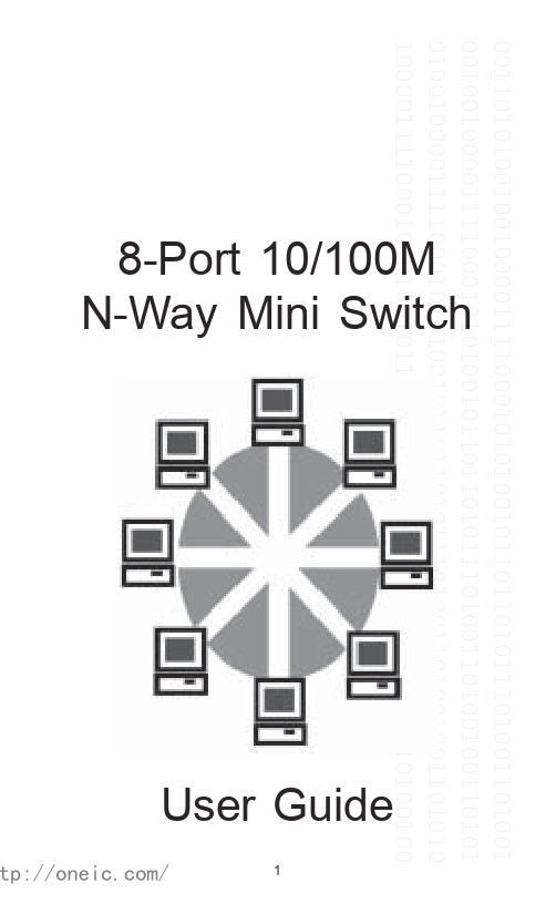
This user guide is applied to the 8 ports 10/100M N-Way Mini Switch . The 8-Port 10/100M N-Way Mini Switch is designed for easy installation and high performance in an environment where traffic on the network and the number of users increase continuously. Small businesses and corporate branch offices can now take full advantage of 100Mbps Fast Ethernet performance and preserve existing desktop investment with no changes required to PCs, NICs, cabling, drivers, or PC configurations.
Performance Highlights
• • • • • • •
DMN3730UFB-7;中文规格书,Datasheet资料

Drain
S D
G
Top View Internal Schematic
Gate
Body Diode
Gate Protection Diode
Source
Equivalent Circuit
ቤተ መጻሕፍቲ ባይዱMax
1 3
0.95 460 560 730
1.2
-
Unit
Test Condition
V
VGS = 0V, ID = 10μA
μA VDS = 30V, VGS = 0V
μA VGS = ±8V, VDS = 0V
V
VDS = VGS, ID = 250μA
VGS = 4.5V, ID = 200mA
VGS = 2.5V
VGS = 2.0V
1.0
VGS = 1.5V
A Product Line of Diodes Incorporated
2.0
VDS = 5V
DMN3730UFB
1.5
1.0
ID, DRAIN CURRENT (A)
ID, DRAIN CURRENT (A)
RDS(ON), DRAIN-SOURCE ON-RESISTANCE (Ω)
Tape width (mm) 8 8
Quantity per reel 3,000 10,000
Marking Information
DMN3730UFB-7
NE
Top View Dot Denotes Drain Side
HTS3005 低电压、低抗性、双向单极性 双变化(SPDT)CMOS模拟开关数据表说明书
Ultra Low ON-Resistance, Low Voltage, Dual, SPDT Analog SwitchGeneral DescriptionThe HTS3005 is a dual, low on-resistance, low voltage, bidirectional, single-pole/double-throw (SPDT) CMOS analog switch designed to operate from a single 1.8V to 5.5V powersupply. Targeted applications include battery powered equipment that benefit from lowR ON (0.5Ω) and fast switching speeds (t ON = 50ns, t OFF = 15ns).The on resistance profile is very flat over the full analog signal range. This ensuresexcellent linearity and low distortion when switching audio signals.The HTS3005 is a committed dual single-pole/double- throw (SPDT) that consist of twonormally open (NO) and two normally close (NC) switches. This configuration can beused as a dual 2-to-1 multiplexer.HTS3005 is available in Green TDFN-3×3-10L and MSOP-10 packages.Featuresn Low Voltage Operation: 1.8V to 5.5Vn Low On-Resistance: 0.5Ω (TYP)n Low On-Resistance Flatnessn-3dB Bandwidth: 15MHzn Fast Switching Times:Øt ON 50nsØt OFF 15nsn Rail-to-Rail Operationn Typical Power Consumption (<0.01µW)n TTL/CMOS Compatiblen Microsize PackagesApplicationn Battery-powered, Handheld, and Portable EquipmentØCellular/Mobile PhonesØLaptops, Notebooks, Palmtopsn Communication Systemsn Sample-and-Hold Circuitsn Audio Signal Routingn Audio and Video Switchingn Portable Test and Measurementn Medical EquipmentUltra Low ON-Resistance, Low Voltage, Dual, SPDT Analog Switch Pin ConfigurationsPin DescriptionSymbol DescriptionV+ Power supply.GND Ground.IN1, IN2Digital control pin to connect the COM terminal to the NO or NC terminals.COM1, COM2Common terminal.NO1, NO2Normally-open terminal.NC1, NC2Normally-closed terminal.Ordering InformationType Number Package Name Package Quantity Marking CodeHTS3005XV10/R6MSOP10 Tape and Reel,3000C3005XHTS3005XF10/R6TDFN-3×3-10 Tape and Reel,3000C3005X Recommended Operating Conditionsn Operating voltage range: 1.8V to 5.5Vn Specified temperature range: -40℃ to 125℃Absolute Maximum RatingsParameter Symbol Absolute Maximum Rating Unit V+ to GND-0.3V to 6V V Analog, Digital voltage range (1)-0.3V to (V+) + 0.3V VContinuous Current NO, NC, or COM±300mA mA Peak Current NO, NC, or COM ±500mA mAOperating Temperature Range -40℃ to +125℃ ℃TemperatureStorage--65℃ to +150℃℃Junction150℃℃Package Thermal Resistance @ TA = 25℃TDFN-3×3-10L, θJA 33℃/W ℃/W MSOP-10, θJA205℃/W ℃/W Lead Temperature (soldering, 10s)260℃℃ESD SusceptibilityHBM2000V V MM400VVAttention: Stresses beyond those listed under Absolute Maximum Ratings may cause permanent damage to the device. Exposure to absolute-maximum-rated conditions for extended periods may affect device reliability.(1) Signals on NC, NO, or COM exceeding V+ will be clamped by internal diodes. Limit forward diode current to maximum current ratings.(2) Stresses beyond those listed under “Absolute Maximum Ratings” may cause permanent damage to the device. These are stress ratings only, and functional operation of the device at these or any other conditions beyond those indicated in the operational sections of the specifications is not implied. Exposure to absolute maximum rating conditions for extended periods may affect device reliability.Ultra Low ON-Resistance, Low Voltage, Dual, SPDT Analog SwitchElectrical CharacteristicsUltra Low ON-Resistance, Low Voltage, Dual, SPDT Analog SwitchV+ = +5V, GND = 0V, TA = -40℃ to +125℃, typical values are at TA = + 25℃, unless otherwise noted SymbolParameterConditionsMin.Typ.Max.UnitANALOG SWITCH V NO ,V NC ,V COM Analog Signal RangeT A =-40℃ to ﹢125℃ 0 V +V R ONOn-Resistance0 ≤ V NO or V NC ≤ V +, I COM = -10mA,Test Circuit 10.50.9ΩT A =-40℃ to ﹢125℃1.1Ω∆R ONOn-Resistance Match Between Channels0 ≤ V NO or V NC ≤ V +, I COM = -10mA,Test Circuit 10.050.09ΩT A =-40℃ to ﹢125℃0.12ΩR FLAT(ON)On-Resistance Flatness0 ≤ V NO or V NC ≤ V +, I COM = -10mA,Test Circuit 10.250.3ΩT A =-40℃ to ﹢125℃0.4ΩLEAKAGE CURRENTS I NC(OFF), I NO(OFF)Source OFF Leakage CurrentV NO or V NC = 4.5V/1V, V COM = 1V/4.5V, V + = +5.5V, Test Circuit 2±4±10nA T A =-40℃ to ﹢125℃±1000nA I NC(ON),I NO(ON), I COM(ON),Channel ON Leakage CurrentV NO or V NC = V COM = 1V or 4.5V, V + = +5.5V, Test Circuit 3±4±10nA T A =-40℃ to ﹢125℃±1000nADIGITAL INPUTS V INH Input High Voltage T A =-40℃ to ﹢125℃ 2.4V V INL Input Low VoltageT A =-40℃ to ﹢125℃0.8V I INL or I INHInput CurrentV IN = V INH or V INL ±0.01±0.1μA T A =-40℃ to ﹢125℃±1μADYNAMIC CHARACTERISTICS t ON Turn-On Time V NO or V NC = 3V, R L = 300Ω, C L = 35pF,Test Circuit 450nS t OFF Turn-Off Time V NO or V NC = 3V, R L = 300Ω, C L = 35pF,Test Circuit 415nS Q Charge Injection C L = 1.0nF, V G = 0V, R G = 0Ω, Test Circuit 520pC t DBreak-Before-MakeTime Delay V NO1 or V NC1 = V NO2 or V NC2 = 3V, R L = 300Ω, C L = 35pF, Test Circuit 6 10nS O ISOOff IsolationR L =50ΩC L = 5pF, TestCircuit 7f = 100kHz -70dB f = 10kHz -85dBElectrical CharacteristicsV+ = +5V, GND = 0V, TA = -40℃ to +125℃, typical values are at TA = + 25℃, unless otherwise notedUltra Low ON-Resistance, Low Voltage, Dual, SPDT Analog SwitchSymbol Parameter Conditions Min.Typ.Max.UnitX TALK Channel-to-ChannelCrosstalkRL= 50Ω,CL= 5pF,Test Circuit 8f = 100kHz -90 dBf = 10kHz-105dBTHD Total HarmonicDistortionf = 20Hz to 20kHz, VCOM=3.5V P-P, RL= 600Ω, CL=50pF0.065 %BW-3dB Bandwidth RL= 50Ω, CL= 5pF, TestCircuit 915 MHZCNC(OFF),CNO(OFF)Source off Capacitance 80 pFCNC(ON),CNO(ON),CCOM(ON)Channel on Capacitance380pF POWER REQUIREMENTSI +Power Supply CurrentV+= +5.5V, VIN= 0V or 5V 0.001μAT A=-40℃ to﹢125℃1μAElectrical CharacteristicsUltra Low ON-Resistance, Low Voltage, Dual, SPDT Analog SwitchV+ = +3V, GND = 0V, TA = -40℃ to +125℃, typical values are at TA = + 25℃, unless otherwise noted.SymbolParameterConditionsMin.Typ.Max.UnitANALOG SWITCH V NO ,V NC ,V COM Analog Signal RangeT A =-40℃ to ﹢125℃ 0 V +V R ONOn-Resistance0 ≤ V NO or V NC ≤ V +, I COM = -10mA,Test Circuit 10.61.0ΩT A =-40℃ to ﹢125℃1.3Ω∆R ONOn-Resistance Match Between Channels0 ≤ V NO or V NC ≤ V +, I COM = -10mA,Test Circuit 10.050.1ΩT A =-40℃ to ﹢125℃0.13ΩR FLAT(ON)On-Resistance Flatness0 ≤ V NO or V NC ≤ V +, I COM = -10mA,Test Circuit 10.250.3ΩT A =-40℃ to ﹢125℃0.4ΩLEAKAGE CURRENTS I NC(OFF), I NO(OFF)Source OFF Leakage CurrentV NO or V NC =3V/1V, V COM = 1V/3V, V + = +3.3V, Test Circuit 2±5±11nA T A =-40℃ to ﹢125℃±1000nA I NC(ON),I NO(ON), I COM(ON),Channel ON Leakage CurrentV NO or V NC = V COM = 1V or 3V, V + = +3.3V, Test Circuit 3±5±11nA T A =-40℃ to ﹢125℃±1000nADIGITAL INPUTS V INH Input High Voltage T A =-40℃ to ﹢125℃ 2.0V V INL Input Low VoltageT A =-40℃ to ﹢125℃0.4V I INL or I INHInput CurrentV IN = V INH or V INL ±0.01±0.1μA T A =-40℃ to ﹢125℃±1μADYNAMIC CHARACTERISTICS t ON Turn-On Time V NO or V NC = 2V, R L = 300Ω, C L = 35pF,Test Circuit 450nS t OFF Turn-Off Time V NO or V NC = 2V, R L = 300Ω, C L = 35pF,Test Circuit 417nS Q Charge Injection C L = 1.0nF, V G = 0V, R G = 0Ω, Test Circuit 525pC t DBreak-Before-MakeTime Delay V NO1 or V NC1 = V NO2 or V NC2 = 2V, R L = 300Ω, C L = 35pF, Test Circuit 6 11nS O ISOOff IsolationR L =50ΩC L = 5pF, TestCircuit 7f = 100kHz -70dB f = 10kHz -85dBElectrical CharacteristicsV+ = +5V, GND = 0V, TA = -40℃ to +125℃, typical values are at TA = + 25℃, unless otherwise notedUltra Low ON-Resistance, Low Voltage, Dual, SPDT Analog SwitchSymbol Parameter Conditions Min.Typ.Max.UnitX TALK Channel-to-ChannelCrosstalkRL= 50Ω,CL= 5pF,Test Circuit 8f = 100kHz -90 dBf = 10kHz-105dBTHD Total HarmonicDistortionf = 20Hz to 20kHz, VCOM=2VP-P, RL= 600Ω, CL=50pF0.06 %BW-3dB Bandwidth RL= 50Ω, CL= 5pF, TestCircuit 915 MHZCNC(OFF),CNO(OFF)Source off Capacitance 80 pFCNC(ON),CNO(ON),CCOM(ON)Channel on Capacitance380pF POWER REQUIREMENTSI +Power Supply CurrentV+= +3.3V, VIN= 0V or 5V 0.001μAT A=-40℃ to﹢125℃1μAUltra Low ON-Resistance, Low Voltage, Dual, SPDT Analog Switch Type Performance CharacteristicsUltra Low ON-Resistance, Low Voltage, Dual, SPDT Analog Switch Application NotesTest Circuit 1. On ResistanceTest Circuit 2. Off Leakage Test Circuit 3. On LeakageTest Circuit 4. Switching TimesTest Circuit 5. Charge InjectionUltra Low ON-Resistance, Low Voltage, Dual, SPDT Analog Switch Application NotesTest Circuit 6. Break-Before-Make Time Delay, tDTest Circuit 7. Off IsolationApplication Notes Data SheetHTS3005Ultra Low ON-Resistance, Low Voltage, Dual, SPDT Analog SwitchTest Circuit 8. Channel-to-Channel CrosstalkTest Circuit 9. -3dB BandwidthPackage OutlinesMSOP-10Data Sheet HTS3005Ultra Low ON-Resistance, Low Voltage, Dual, SPDT Analog SwitchHTS3005Data Sheet Ultra Low ON-Resistance, Low Voltage, Dual, SPDT Analog Switch Package OutlinesTDFN-3×3-10L。
奥美晨曦系列微波传感器说明书
OS100 SERIES Mini-Infrared Transmitter e-mail:**************For latest product manuals: Shop online at User’s G ui d e***********************Servicing North America:U.S.A. Omega Engineering, Inc.Headquarters: Toll-Free: 1-800-826-6342 (USA & Canada only)Customer Service: 1-800-622-2378 (USA & Canada only)Engineering Service: 1-800-872-9436 (USA & Canada only)Tel: (203) 359-1660 Fax: (203) 359-7700e-mail:**************For Other Locations Visit /worldwideThe information contained in this document is believed to be correct, but OMEGA accepts no liability for any errors it contains, and reserves the right to alter specifications without notice.Table of ContentsSection ...................................................................PageSafety Warnings and IEC Symbols (iii)Caution and Safety Information (iii)Section 1 Introduction ....................................................................1-1Section 2Installation ......................................................................1-12.1 Unpacking and Inspection ......................................1-12.2 Electrical Connection ..............................................2-1Section 3Operation ........................................................................3-13.1 Main Board ................................................................3-13.2 Ambient Temperature ..............................................3-23.3 Atmospheric Quality ................................................3-33.4 Measuring Temperature ..........................................3-33.5 Alarm Setting ............................................................3-43.6 Adding Extension Cable...........................................3-4Section 4 Laser Sight Accessory ...................................................4-14.1 Warning and Cautions .............................................4-14.2 Operating the Laser Sight Accessory .....................4-1Section 5 Specifications .................................................................5-15.1 General .......................................................................5-15.2 Laser Sight Accessory (OS100-LS) ..........................5-2Section 6Emissivity Table .............................................................6-1iTable of FiguresFigure Description Page2-1Power Supply & Analog Output Connections ..........2-12-2 Alarm Output Connection ............................................2-13-1 Main PC Board ...............................................................3-23-2 Sensor..............................................................3-2Housing3-3 Optical Field of View .....................................................3-43-4Setting the Temperature Engineering Unit..................3-43-5Mounting Bracket OS100-MB .......................................3-53-6Water Cooling Jacket, OS100-WC ................................3-53-7Typical Water Cool Jacket Assembly ...........................3-53-8Air Purge Collar, OS100-AP..........................................3-63-9DIN Rail Mounting Adapter, OS100-DR ....................3-63-10NEMA-4 Aluminum Enclosure ....................................3-64-1Laser Sighting Accessory, OS100-LS ............................4-24-2Laser Warning Label ......................................................4-2iiSafety Warnings and IEC SymbolsThis device is marked with international safety and hazard symbols in accordance with IEC 1010. It is important to read and follow all precautions and instructions in this manual before operating or commissioning this device as it contains important information relating to safety and EMC. Failure to follow all safety precautions may result in injury and or damage to your calibrator. IEC symbols DescriptionCaution and Safety Information• If the equipment is used in a manner not specified in this manual, the protection provided by the equipment may be impaired.• The installation category is one (1).• There are no user replaceable fuses in this product• The output terminals of this product are for use with equipment (digital meters, chart recorders, etc,) which have no accessible five parts. Such equipment should comply with all the applicable safety requirements.• Do not operate the equipment in flammable or explosive environments.• All connections to the thermometer should be made via a shielded cable, 24 AWG stranded wire with the following ratings: 300V , 105°C (221°F), PVC insulation.• Power must be disconnected before making any electrical connections.• The power supply used to power the thermometer should be VDE or UL approved with the following ratings: 12 to 24vdc @150mA with overload protection of 500mA.iiiCaution, refer to accompanying documentsDirect Current Laser SymbolFrame or ChassisNOTES: ivSection 1 - IntroductionThe low cost OS101 mini-infrared transmitter provides non-contacttemperature measurement for industrial applications. The unit measures atemperature range of -18 to 538°C (0-1000°F) and provides a linear analogoutput of either 4-20 mA, 0-5 VDC, K type TC, 1 mV/°C, or 1 mV/°F.The new OS102 mini-infrared transmitter has all the functions of OS101plus a built-in LED display that shows the measured temperature indegrees F or degrees C which is switchable in the field.The miniature sensor head design 2.5 cm dia. x 6.3 cm Length (1" x 2.5") isideal for measuring temperature in confined, and hard to reach places.The aluminum sensor head as well as the rugged electronic housing (Diecast Aluminum) are NEMA-4 rated.The sensor head is connected to the electronic housing via a 1.82 m (6 feet)shielded cable as standard. The unit provides field adjustable alarmoutput.Section 2 - Installation2.1UnpackingRemove the packing list and verify that you have received all yourequipment. If you have any questions about the shipment, please callCustomer Service at:1-800-622-2378 or 203-359-1660. We can also be reached on the internet:e-mail:**************When you receive the shipment, inspect the container and equipment forany signs of damage. Note any evidence of rough handling in transit.inspection. After examination and removing contents, save packing material and carton in theevent reshipment is necessary.The following items are supplied in the box:• The infrared transmitter including the sensor head and the 1.82 m(6 feet) shielded cable• User's Manual• Mounting Nut1-1The following describes the ordering information:OS102 or OS101 - MA- *,**, where The following optional accessories are available:Here are the Features of OS101 and OS102 infrared transmitters:2.2Electrical Connection Sensor Head Cable - The Sensor head is pre-wired to a 1.8 m (6 feet)shielded cable. Plug & lock-in the male connector to the mating female connector on the aluminum housing.Power & Output Connection - Open the cover of the main aluminum housing. Slide the cable through the strain relief and connect the wires to the terminal block on the board as shown in Fig. 2-1. For Alarm output connection, refer to Fig. 2-2.2-1MA - 4/20 mA output V1 - 0 to 5 VDC output K - Thermocouple output, K type MV - Millivolt output C - 1 mV/°C output F - 1 mV/°F output HT- High temperature sensor head3-1Figure 2-2. Alarm Output Connection Section 3 - Operation3-1Main BoardThe Main Board is shown in Fig. 3-1. Here are the important components on the board:(1) - Terminal Block for Power & Output connections(2) - Single Turn Potentiometer to adjust Emissivity in tenths (0.x_)(3) - Single Turn Potentiometer to adjust Emissivity in hundreds (0._x)(4) -Slide switch to select between real time (Normal Operation) and alarm set point(5) - Alarm set point adjust, P4(6) - Sensor Head connection(7) - Input Zero adjust, P3(8) - Input Span adjust, P2(9) - Output Zero adjust, P5(10) - Output Span adjust, P6Figure 3-1. Main PC Board3.2Ambient TemperatureThe Sensing head can operate in an ambient temperature of 0 to 70°C (32to 158°F). The Sensing head in the high temperature model (-HT) can operate in an ambient temperature of 0 to 85°C (32 to 185°F) without any cooling required. The Sensing head can operate up to 200°C (392°F) using the water cool jacket accessory OS100-WC (See Fig. 3-6).There is a warm up period of 3 minutes after power up. After the warm up period, temperature measurement can be made.When the ambient temperature around the sensor head changes abruptly,the sensor head goes through thermal shock. It takes a certain amount of time for the sensor head to stabilize to the new ambient temperature. For example, it takes about 30 minutes for the sensor head to stabilize going from 25°C to 50°C (77 to 122°F) ambient temperature.The sensor head dimensions are shown in Fig. 3-2.Figure 3-2. Sensor Housing3-23-33.3Atmospheric QualityEnvironments with smoke, dust, and fumes dirty up the optical lens, and cause erroneous temperature readings. To keep the surface of the optical lens clean, the air purge collar accessory is recommended, OS100-AP , See Fig. 3-7.3.4Measuring TemperatureBefore starting to measure temperature, make sure that the following check list is met:ߜ The power and analog output connections are made (Fig. 2-1).ߜThe sensor head is connected to the main unit.ߜThe slide switch (SW1) on the main board is set to real time (Fig. 3-1).ߜThe target is larger than the optical field of view of the sensor head (Fig. 3-3).ߜThe emissivity adjustment on the main board is set properly (Fig. 3-1).ߜThe output load is within the product specification.On OS102 transmitters, follow these additional steps:ߜ The temperature display is set to °F or °C (Fig. 3-4)ߜ For 4-20mA output models, make sure an output load is added, ie. 250ohms.Figure 3-3. Optical Field Of ViewFigure 3-4. Setting the Temperature Engineering Unit3.5Alarm SettingThe unit provides 0-100% alarm set point adjustment. Here is an exampleof an alarm setting.• An OS101-MA(4/20 mA output), the alarm is to be set at 400°Ftemperature.• Connect the alarm output as shown in Fig. 2-2.• Set the slide switch (SW1) on the main board to the Alarm position.• Measure the analog output, and set the Potentiometer P4 until theoutput reads 10.4 mA which is 40% (400°F) of the temperature range.40 x (20-4)[10.4mA=+ 4]100• Set the slide switch (SW1) back to the Real Time position.• If the temperature reading is below the alarm set point, the alarmoutput stays high, otherwise it goes low.On the OS102, you can set the alarm set point directly based on thetemperature display.3.6Adding Extension CableYou can add extension cable between the Sensor Head and the mainelectronic housing up to 15.2 m (50 feet). After adding the extension cable,the Zero input potentiometer, P3 may be re-adjusted. (See Fig. 3-1, forproper analog output reading)The following figures show the mounting bracket (OS100-MB), Watercooling jacket (OS100-WC), Air purge collar (OS100-AP), DIN RailMounting adapter (OS-100-DR), and the main aluminum enclosure. TheDIN Rail Mounting adapter (OS100-DR) is mounted to the bottom of themain aluminum enclosure using two 4-40 screws.A typical water cool jacket assembly is shown in Fig. 3-7, on the following page.1. Mounting Nut2. Mounting Bracket3. Water Cool Jacket4. Sensor Head3-4Figure 3-5. Mounting Bracket OS100-MBFigure 3-6. Water Cooling Jacket, OS100-WCFigure 3-7. Typical Water Cool Jacket Assembly3-5Figure 3-8. Air Purge Collar, OS100-APFigure 3-9. DIN Rail Mounting Adapter, OS-100-DRFigure 3-10. NEMA-4 Aluminum Enclosure3-6Section 4 - Laser Sight Accessory4.1Warning and Cautionsbelow:•Use of controls or adjustments or performance of procedures other than those specified here may result in hazardous radiation exposure.• Do not look at the laser beam coming out of the lens or view directly with optical instruments - eye damage can result.• Use extreme caution when operation the laser sight accessory • Never point the laser accessory at a person • Keep out of the reach of all children4.2Operating the Laser Sight AccessoryThe laser sight accessory screws onto the front of the sensor head. This accessory is only used for alignment of the sensor head to the target area.After the alignment process, the accessory has to be removed from the front of the sensor head before temperature measurement.The laser sight accessory is powered from a small compact battery pack (included with the accessory). Connect the battery pack to the accessory using the cable provided. Aim at the target, and turn on the battery power using the slide switch on the battery pack. Adjust the sensor head position so that the laser beam points to the center of the target area. Turn off the battery pack, and remove the laser sighting accessory from the sensor head. See Fig. 4-1 for reference.4-14-2Figure 4-2. Laser Warning LabelSection 5 - Specifications5.1 - GeneralTemperature Range-18 to 538°C (0 to 1000°F)Accuracy @ 22°C (72°F)±2% of Rdg. or 2.2°C (4°F) whichever is ambient temperature & greateremissivity of 0.95 or greaterOptical Field of View6:1 (Distance/Spot Size)Repeatability±1% of Rdg.Spectral Response 5 to 14 micronsResponse Time150 msec (0 to 63% of final value)Emissivity Range0.1 to 0.99, adjustableOperating Ambient TemperatureMain Transmitter0 to 50°C (32 to 122°F)Sensor Head0 to 70°C (32 to 158°F)Sensor Head (-HT Model)0 to 85°C (32 to 185°F)Sensor Head with OS100-WC(Water Cooling Jacket)0 to 200°C (32 to 392°F)Operating Relative Humidity Less than 95% RH, non-condensingWater Flow Rate for OS100-WC0.25 GPM, room temperatureThermal Shock About 30 minutes for 25°Cabrupt ambient temperature change Warm Up Period 3 minutesAir Flow Rate for OS100-AP 1 CFM (0.5 Liters/sec.)Power12 to 24 VDC @ 100 mAAnalog OutputsMV-F 1 mV/°FMV-C 1 mV/°CK K Type TC - OS101 onlyMA 4 to 20 mAV10 to 5 VDCOutput Load requirementsMin. Load (0 to 5VDC) 1 K-OhmsMax. Load (4 to 20 mA)(Supply Power - 4 )/20 mATransmitter Housing NEMA-4 & IP65, Die Cast AluminumSensor Head Housing NEMA-4 , AluminumAlarm Output Open Drain, 100 mAAlarm Set Point0 to 100% , Adjustable via P4Alarm Deadband14°C (25°F)5-15-25.1 - General Con’t.DimensionsSensor Head25.4 OD. x 63.5 mm L(1" OD. x 2.5" L)Main Housing, OS10165.5 W x 30.5 H x 115.3 mm L(2.58" W x 1.2" H x 4.54" L)Main Housing, OS10265.5 W x 55.9 H x 115.3 mm L(2.58" W x 2.2" H x 4.54" L)Weight 272 g (0.6 lb)5.2Laser Sight Accessory (OS100-LS)Wavelength (Color)630 - 670 nm (Red)Operating Distance (Laser Dot)Up to 9.1 m (30 ft.)Max. Output Optical Power Less than 1 mW at 22°F ambienttemperature.European Classification Class 2, EN60825-1/11.2001Maximum Operating current45 mA at 3 VDCFDA Classification Complies with 21 CFR 1040.10,Class II Laser ProductBeam Diameter 5 mmBeam Divergence< 2 mradOperating Temperature0 to 50°C (32 to 122°F)Operating Relative Humidity Less than 95% RH, non-condensingPower Switch ON / OFF , Slide switch on the BatteryPackPower Indicator Red LEDPower Battery Pack, 3 VDC (Consists of two 1.5VDC AA size Lithium Batteries) Laser Warning Label Located on the head sight circumferenceIdentification Label Located on the head sight circumferenceDimensions38 DIA x 50.8 mm L(1.5" DIA x 2" L)Section 6 - Emissivity Table6-1Material Emissivity (ε)Aluminum – pure highly polished plate . . . . . . . . . . . . . . . . . . . . . . . . 0.04 to 0.06Aluminum – heavily oxidized . . . . . . . . . . . . . . . . . . . . . . . . . . . . . . . 0.20 to 0.31Aluminum – commercial sheet . . . . . . . . . . . . . . . . . . . . . . . . . . . . . . . . . . . . 0.09Brass – dull plate. . . . . . . . . . . . . . . . . . . . . . . . . . . . . . . . . . . . . . . . . . . . . . 0.22Brass – highly polished, 73.2% Cu, 26.7% Zn. . . . . . . . . . . . . . . . . . . . . . . . . 0.03Chromium – polished. . . . . . . . . . . . . . . . . . . . . . . . . . . . . . . . . . . . . 0.08 to 0.36Copper – polished. . . . . . . . . . . . . . . . . . . . . . . . . . . . . . . . . . . . . . . . . . . . . 0.05Copper – heated at 600°C (1112°F). . . . . . . . . . . . . . . . . . . . . . . . . . . . . . . 0.57Gold – pure, highly polished or liquid. . . . . . . . . . . . . . . . . . . . . . . . . 0.02 to 0.04Iron and steel (excluding stainless)– polished iron . . . . . . . . . . . . . . . . 0.14 to 0.38Iron and steel (excluding stainless)– polished cast iron. . . . . . . . . . . . . . . . . . . 0.21Iron and steel (excluding stainless)– polished wrought iron . . . . . . . . . . . . . . . 0.28Iron and steel (excluding stainless)– oxidized dull wrought iron . . . . . . . . . . . . 0.94Iron and steel (excluding stainless)– rusted iron plate . . . . . . . . . . . . . . . . . . . 0.69Iron and steel (excluding stainless)– polished steel. . . . . . . . . . . . . . . . . . . . . . 0.07Iron and steel (excluding stainless)– polished steel oxidized at600°C (1112°F). . . . . . . . . . . . . . . . . . . . 0.79Iron and steel (excluding stainless)– rolled sheet steel . . . . . . . . . . . . . . . . . . . 0.66Iron and steel (excluding stainless)– rough steel plate . . . . . . . . . . . . . 0.94 to 0.97Lead – gray and oxidized . . . . . . . . . . . . . . . . . . . . . . . . . . . . . . . . . . . . . . . 0.28Mercury . . . . . . . . . . . . . . . . . . . . . . . . . . . . . . . . . . . . . . . . . . . . . 0.09 to 0.12Molybdenum filament . . . . . . . . . . . . . . . . . . . . . . . . . . . . . . . . . . . . 0.10 to 0.20Nickel – polished . . . . . . . . . . . . . . . . . . . . . . . . . . . . . . . . . . . . . . . . . . . . . 0.07Nickel – oxidized at 649 to 1254°C (1200°F to 2290°F). . . . . . . . . . . 0.59 to 0.86Platinum – pure polished plate . . . . . . . . . . . . . . . . . . . . . . . . . . . . . . 0.05 to 0.10Platinum – wire . . . . . . . . . . . . . . . . . . . . . . . . . . . . . . . . . . . . . . . . 0.07 to 0.18Silver – pure and polished . . . . . . . . . . . . . . . . . . . . . . . . . . . . . . . . . 0.02 to 0.03Stainless steel – polished . . . . . . . . . . . . . . . . . . . . . . . . . . . . . . . . . . . . . . . . 0.07Stainless steel – Type 301 at 232 to 942°C (450°F to 1725°F). . . . . . . 0.54 to 0.63Tin – bright . . . . . . . . . . . . . . . . . . . . . . . . . . . . . . . . . . . . . . . . . . . . . . . . . 0.06Tungsten – filament . . . . . . . . . . . . . . . . . . . . . . . . . . . . . . . . . . . . . . . . . . . . 0.39Zinc – polished commercial pure . . . . . . . . . . . . . . . . . . . . . . . . . . . . . . . . . . 0.05Zinc – galvanized sheet. . . . . . . . . . . . . . . . . . . . . . . . . . . . . . . . . . . . . . . . . 0.23M E T A L S6-2Material Emissivity (ε) Asbestos Board . . . . . . . . . . . . . . . . . . . . . . . . . . . . . . . . . . . . . . . . . . . . . . .0.96 Asphalt, tar, pitch . . . . . . . . . . . . . . . . . . . . . . . . . . . . . . . . . . . . . . .0.95 to 1.00 Brick– red and rough . . . . . . . . . . . . . . . . . . . . . . . . . . . . . . . . . . . . . . . . . .0.93 Brick– fireclay . . . . . . . . . . . . . . . . . . . . . . . . . . . . . . . . . . . . . . . . . . . . . . .0.75 Carbon– filament . . . . . . . . . . . . . . . . . . . . . . . . . . . . . . . . . . . . . . . . . . . . .0.53 Carbon– lampblack - rough deposit . . . . . . . . . . . . . . . . . . . . . . . . . .0.78 to 0.84 Glass- Pyrex, lead, soda . . . . . . . . . . . . . . . . . . . . . . . . . . . . . . . . . .0.85 to 0.95 Marble– polished light gray . . . . . . . . . . . . . . . . . . . . . . . . . . . . . . . . . . . . .0.93 Paints, lacquers, and varnishes– Black matte shellac . . . . . . . . . . . . . . . . . . . .0.91 Paints, lacquers, and varnishes– aluminum paints . . . . . . . . . . . . . . . .0.27 to 0.67 Paints, lacquers, and varnishes– flat black lacquer . . . . . . . . . . . . . . .0.96 to 0.98 Paints, lacquers, and varnishes– white enamel varnish . . . . . . . . . . . . . . . . . .0.91 Porcelain– glazed . . . . . . . . . . . . . . . . . . . . . . . . . . . . . . . . . . . . . . . . . . . . .0.92 Quartz– opaque . . . . . . . . . . . . . . . . . . . . . . . . . . . . . . . . . . . . . . . .0.68 to 0.92 Roofing Paper . . . . . . . . . . . . . . . . . . . . . . . . . . . . . . . . . . . . . . . . . . . . . . .0.91 Tape– Masking . . . . . . . . . . . . . . . . . . . . . . . . . . . . . . . . . . . . . . . . . . . . . .0.95 Water . . . . . . . . . . . . . . . . . . . . . . . . . . . . . . . . . . . . . . . . . . . . . . . .0.95 to 0.96 Wood– planed oak . . . . . . . . . . . . . . . . . . . . . . . . . . . . . . . . . . . . . . . . . . . .0.90 NONMETALSNOTES:6-3NOTES: 6-4OMEGA’s policy is to make running changes, not model changes, whenever an improvement is possible. T his affords our customers the latest in technology and engineering.OMEGA is a trademark of OMEGA ENGINEERING, INC.© Copyright 2017 OMEGA ENGINEERING, INC. All rights reserved. T his document may not be copied, photocopied, reproduced, translated, or reduced to any electronic medium or machine-readable form, in whole or in part, without the prior written consent of OMEGA ENGINEERING, INC.FOR WARRANTY RETURNS, please have the following information available BEFORE contacting OMEGA:1. P urchase Order number under which the product was PURCHASED,2. M odel and serial number of the product under warranty, and3. Repair instructions and/or specific problems relative to the product.FOR NON-WARRANTY REPAIRS, consult OMEGA for current repair charges. Have the following information available BEFORE contacting OMEGA:1. Purchase Order number to cover the COST of the repair,2. Model and serial number of the product, and 3. Repair instructions and/or specific problems relative to the product.RETURN REQUESTS/INQUIRIESDirect all warranty and repair requests/inquiries to the OMEGA Customer Service Department. BEFORE RET URNING ANY PRODUCT (S) T O OMEGA, PURCHASER MUST OBT AIN AN AUT HORIZED RET URN (AR) NUMBER FROM OMEGA’S CUST OMER SERVICE DEPART MENT (IN ORDER T O AVOID PROCESSING DELAYS). The assigned AR number should then be marked on the outside of the return package and on any correspondence.T he purchaser is responsible for shipping charges, freight, insurance and proper packaging to preventbreakage in transit.WARRANTY/DISCLAIMEROMEGA ENGINEERING, INC. warrants this unit to be free of defects in materials and workmanship for a period of 25 months from date of purchase. OMEGA’s WARRANTY adds an additional one (1) month grace period to the normal two (2) year product warranty to cover handling and shipping time. This ensures that OMEGA’s customers receive maximum coverage on each product.If the unit malfunctions, it must be returned to the factory for evaluation. OMEGA’s Customer Service Department will issue an Authorized Return (AR) number immediately upon phone or written request. Upon examination by OMEGA, if the unit is found to be defective, it will be repaired or replaced at no charge. OMEGA’s WARRANT Y does not apply to defects resulting from any action of the purchaser, including but not limited to mishandling, improper interfacing, operation outside of design limits, improper repair, or unauthorized modification. T his WARRANT Y is VOID if the unit shows evidence of having been tampered with or shows evidence of having been damaged as a result of excessive corrosion; or current, heat, moisture or vibration; improper specification; misapplication; misuse or other operating conditions outside of OMEGA’s control. Components in which wear is not warranted, include but are not limited to contact points, fuses, and triacs.OMEGA is pleased to offer suggestions on the use of its various products. However, OMEGA neither assumes responsibility for any omissions or errors nor assumes liability for any damages that result from the use of its products in accordance with information provided by OMEGA, either verbal or written. OMEGA warrants only that the parts manufactured by the company will be as specified and free of defects. OMEGA MAKES NO OTHER WARRANTIES OR REPRESENTATIONS OF ANY KIND WHATSOEVER, EXPRESSED OR IMPLIED, EXCEPT THAT OF TITLE, AND ALL IMPLIED W ARRANTIES INCLUDING ANY W ARRANTY OF MERCHANTABILITY AND FITNESS FOR A PARTICULAR PURPOSE ARE HEREBY DISCLAIMED. LIMITATION OF LIABILITY: The remedies of purchaser set forth herein are exclusive, and the total liability of OMEGA with respect to this order, whether based on contract, warranty, negligence, indemnification, strict liability or otherwise, shall not exceed the purchase price of the component upon which liability is based. In no event shall OMEGA be liable for consequential, incidental or special damages.CONDITIONS: Equipment sold by OMEGA is not intended to be used, nor shall it be used: (1) as a “Basic Component” under 10 CFR 21 (NRC), used in or with any nuclear installation or activity; or (2) in medical applications or used on humans. Should any Product(s) be used in or with any nuclear installation or activity, medical application, used on humans, or misused in any way, OMEGA assumes no responsibility as set forth in our basic WARRANT Y /DISCLAIMER language, and, additionally, purchaser will indemnify OMEGA and hold OMEGA harmless from any liability or damage whatsoever arising out of the use of theProduct(s) in such a manner.Where Do I Find Everything I Need forProcess Measurement and Control?OMEGA…Of Course!Shop online at TEMPERATUREM U Thermocouple, RTD & Thermistor Probes, Connectors,Panels & AssembliesM U Wire: Thermocouple, RTD & ThermistorM U Calibrators & Ice Point ReferencesM U Recorders, Controllers & Process MonitorsM U Infrared PyrometersPRESSURE, STRAIN AND FORCEM U Transducers & Strain GagesM U Load Cells & Pressure GagesM U Displacement TransducersM U Instrumentation & AccessoriesFLOW/LEVELM U Rotameters, Gas Mass Flowmeters & Flow ComputersM U Air Velocity IndicatorsM U Turbine/Paddlewheel SystemsM U Totalizers & Batch ControllerspH/CONDUCTIVITYM U pH Electrodes, Testers & AccessoriesM U Benchtop/Laboratory MetersM U Controllers, Calibrators, Simulators & PumpsM U Industrial pH & Conductivity EquipmentDATA ACQUISITIONM U Communications-Based Acquisition SystemsM U Data Logging SystemsM U Wireless Sensors, Transmitters, & ReceiversM U Signal ConditionersM U Data Acquisition SoftwareHEATERSM U Heating CableM U Cartridge & Strip HeatersM U Immersion & Band HeatersM U Flexible HeatersM U Laboratory HeatersENVIRONMENTALMONITORING AND CONTROLM U Metering & Control InstrumentationM U RefractometersM U Pumps & TubingM U Air, Soil & Water MonitorsM U Industrial Water & Wastewater TreatmentM U pH, Conductivity & Dissolved Oxygen InstrumentsM3572/1217。
D53G-026.0M;D53G-020.0M-T;D53G-026.0M-T;D53G-020.0M;中文规格书,Datasheet资料
Specifications subject to change without notice. All dimensions in inches. © Copyright 2011 The Connor-Winfield CorporationPrecision5.0x 3.2mm TCXO In Stock at Digi-KeyDescription:The Connor-Winfield D53G is a 3.3V Clipped Sinewave, Surface Mount, T emperature Compensated Crystal Oscillator (TCXO) designed forapplications requiring tight frequency stability. The RoHS compliant surface mount package is designed for high-density mounting and is optimum for mass production.Operating SpecificationsParameterMinimumNominal MaximumUnits NotesCenter Frequency (Fo) -20.0 or 26.0- MHz Freq. Stability vs. Cal. @ 25°C -1.0 - 1.0 ppm 1Freq. Stability vs. Temp. -0.50 - 0.50 ppm 2Freq. Stability vs. Voltage -0.25 - 0.25 ppm ±5%Freq. Stability vs. Load -0.25 - 0.25 ppm ±5%Static Temperature Hysteresis - - 0.40 ppm 3Freq. shift after reflow soldering -1.0 - 1.0 ppm 4Aging -1.0 - 1.0 ppm/yearOperating Temperature Range: -30 - 85 °C Supply Voltage (Vcc) 3.135 3.3 3.465 Vdc ±5%Supply Current (Icc) - - 2 mA Period Jitter - 3 5 ps rms Integrated Phase Jitter - 0.5 1.0 ps rms 5SSB Phase Noise at 10Hz offset - -80 - dBc/Hz SSB Phase Noise at 100Hz offset - -110 - dBc/Hz SSB Phase Noise at 1KHz offset - -130 - dBc/Hz SSB Phase Noise at 10KHz offset - -145 - dBc/Hz SSB Phase Noise at 100KHz offset - -150 - dBc/Hz Start-up Time--5msAbsolute Maximum RatingsParameterMinimumNominalMaximumUnitsNotesStorage Temperature -55 - 85 °C Supply Voltage (Vcc)-0.5-Vcc+0.5VdcFeatures:Model: D53GTCXO3.3 Vdc OperationClipped Sinewave OutputFrequency Stability: ±0.50 ppm T emperature Range: -30 to 85°C Low Jitter <1ps RMS5.0x3.2mm SMT Package T ape and Reel Packaging RoHS Compliant, Lead FreeBulletin TX239Page 1 of 2Revision 02Date03 Nov 2011Clipped Sinewave Output CharacteristicsParameterMinimumNominalMaximumUnitsNotesOutput Voltage 1.0 - - V pk-pk 6Load Resistance - 10K - Ohm Load Capacitance -10-pF7Package CharacteristicsPackageHermetically sealed ceramic package and metal coverD 53G114420.0M H ZEnvironmental CharacteristicsVibration: Vibration per Mil Std 883E Method 2007.3 Test Condition AShock: Mechanical Shock per Mil Std 883E Method 2002.4 Test Condition B.Soldering Process; RoHS compliant lead free. See soldering profile on page 2.Notes:1. Frequency Calibration; frequency measured at Vcc = 3.3 Vdc, 25°C, referenced to Fo.2. Frequency stability vs. change in temperature. [±(Fmax - Fmin)/2.Fo].3. Frequency change after reciprocal temperature ramped over the operating range. Frequency measured before and after at 25°C.4. Within two hours after reflow soldering5. BW=12K Hz to 20 MHz.6. Output is DC coupled7. For best performance it is recommended that the circuit connected to this output should have an equivalent input capacitance of 10 pF.Ordering InformationD53G-020.0M* or D53G-026.0M** For the tape and reel option, add -T to the end of the part number. Example: D53G-020.0M-TSpecifications subject to change without notice. All dimensions in inches. © Copyright 2011 The Connor-Winfield Corporation2111 Comprehensive Drive Aurora, Illinois 60505Phone: 630-851-4722Fax: BulletinTX239Page 2 of 2Revision 02Date03 Nov 2011Test CircuitOutput WaveformTape and Reel InformationSolder ProfileMeets IPC/JEDEC J-STD-020C200mV/Div45236781Vcc Supply VoltageN/CDNC DNC DNC.01uF BypassOutput10pF**10Kohm DNCAC Coupling CapacitorDNC =Do Not Connect **NPO GradeComponent1: N/C2: Do Not Connect 3: Do Not Connect 4: Ground 5: Output6: Do Not Connect 7: Do Not Connect 8: Supply Voltage (Vcc)Pad ConnectionsSuggested Pad LayoutPackage LayoutTo * Keep Out Area: Do not route any traces in the keep out area. It is recommended the next layer under the keep out area is tobe ground plane.0.065ViewDimensional Tolerance:+/-0.005(+/-0.127mm)Phase Noise PlotModel D53G-020.0MHZ分销商库存信息:CONNOR-WINFIELDD53G-026.0M D53G-020.0M-T D53G-026.0M-T D53G-020.0M。
★MDM300.I.S★
英国密析尔MICHELL 仪表制造商露点变送器,dewpointmeters ,冷/冷镜湿度计,相对湿度传感器,过程水分测定仪,碳氢露点分析仪,液体分析仪中的水分和氧气分析仪,是一家国际领先的高精度传感与结束在该领域有30多年的经验。
我们的产品范围的高精度电容湿度传感器,帮助客户测量微量水分,在其过程中的应用,而我们的相对湿度变送器,相对湿度和温度传感器被广泛应用于HV AC 应用,药品储存等生产流程控制的环境条件是至关重要的。
,再加上我们的参考露点湿度计,湿度校准系统使客户能够进行校准便携式湿度计和相对湿度的仪器内部的,节省费用和停机时间。
我们提供高速测量中的应用范围,包括发电站,燃烧优化控制CO 2的水平啤酒厂,清洁气体的过程,如硅片生产和纯气体生成氧气。
天然气行业和发电厂的客户节省数百万美元的维修和停机时间,通过使用我们的康达迈科Condumax II 烃露点分析仪,以确保传输的天然气质量在贸易交接,防止燃气燃烧器故障,延长寿命过程的设备。
我们在烃类液体中的水分分析仪适用于防爆,本质安全和实验室版本,并允许范围广泛的烃类液体,包括变压器油,液压油,石油馏分和纯烃中的水分含量的连续测量。
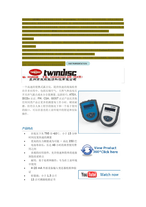
一个高速的便携式露点仪,提供快速的现场检查在许多应用中,包括压缩空气,天然气和高电压开关淬气露点或水分含量测量。
这款轻巧,ATEX ,IECEx 认证,FM ,CSA ,GOST 认证产品比其他任何同类产品让更多的测量每工作小时。
硬质耐磨,但符合人体工程学的情况下和一个易于使用的接口,可以在恶劣的工业环境中的舒适和实际操作。
产品特点∙ 在低压下从T95至-60℃,小于15分钟时间反复快速的测量∙ 更高的压力测量成为可能 - 高达350巴 ∙ 电池寿命长:长达48小时的典型使用费用之间∙ 直观的应用套件,允许快速和简单的连接到您的采样点∙ 耐用,易于处理和操作:专为在工业环境中使用∙ 4-20 mA 外部设备输入变送器校准和验证∙ 轻量级:小于1.5公斤 ∙13点可溯源校准证书MDM300的MDM300采样选项MDM300 MDM300要获得最佳性能,它是为您的测量点有适当的样品调节至关重要。
DMN5L06VK-7;DMN5L06VAK-7;中文规格书,Datasheet资料

1
3 of 6
VGS, GATE SOURCE VOLTAGE (V) Fig. 6 Static Drain-Source On-Resistance
Packaging 3,000/Tape & Reel 10,000/Tape & Reel 3,000/Tape & Reel 10,000/Tape & Reel 3,000/Tape & Reel 10,000/Tape & Reel
1. No purposely added lead. Fully EU Directive 2002/95/EC (RoHS) & 2011/65/EU (RoHS 2) compliant. 2. See for more information about Diodes Incorporated’s definitions of Halogen- and Antimony-free, "Green" and Lead-free. 3. Halogen- and Antimony-free "Green” products are defined as those which contain <900ppm bromine, <900ppm chlorine (<1500ppm total Br + Cl) and
VGS(th)
0.49
⎯
⎯
⎯
RDS (ON)
⎯
⎯
⎯
⎯
ID(ON)
0.5
1.4
|Yfs|
SGM3005XMS中文资料
PIN DESCRIPTION
NAME
V+ GND IN1, IN2 COM1, COM2 NO1, NO2 NC1, NC2
PIN
1 6 4,8 3,9 2,10 5,7
FUNCTION
Power supply ground Digital control pin to connect the COM terminal to the NO or NC terminals Common terminal Normally-open terminal Normally-closed terminal
VNO or VNC = 3V, RL = 300Ω, CL = 35pF, Test Circuit 4 VNO or VNC = 3V,
Stresses beyond those listed under “Absolute Maximum Ratings” may cause permanent damage to the device. These are stress ratings only, and functional operation of the device at these or any other conditions beyond those indicated in the operational sections of the specifications is not implied. Exposure to absolute maximum rating conditions for extended periods may affect device reliability. (1) Signals on NC, NO, or COM or IN exceeding V+ will be clamped by internal diodes. Limit forward diode current to maximum current ratings.
DMN6068LK3-13;中文规格书,Datasheet资料

A Product Line ofDiodes IncorporatedDMN6068LK360V N-CHANNEL ENHANCEMENT MODE MOSFETProduct SummaryV (BR)DSSR DS(on) I D T A = 25°C 60V68m Ω @ V GS = 10V 8.5A 100m Ω @ V GS = 4.5V7.0ADescription and ApplicationsThis MOSFET has been designed to minimize the on-state resistance (R DS(on)) and yet maintain superior switching performance, making it ideal for high efficiency power management applications.• Motor Control• Transformer Driving Switch • DC-DC Converters• Power Management Functions •Uninterrupted Power SupplyFeatures and Benefits• 100% Unclamped Inductive Switch (UIS) test in production • Low on-resistance • Fast switching speed• “Green” component and RoHS compliant (Note 1) •Qualified to AEC-Q101 Standards for High ReliabilityMechanical Data• Case: TO252-3L • Case Material: Molded Plastic, “Green” Molding Compound. ULFlammability Classification Rating 94V-0 (Note 1) • Moisture Sensitivity: Level 1 per J-STD-020 • Terminals Connections: See Diagram• Terminals: Matte Tin Finish annealed over Copper leadframe. Solderable per MIL-STD-202, Method 208 •Weight: 0.33 grams (approximate)Ordering Information (Note 1)Product Marking Reel size (inches) Tape width (mm)Quantity per reelDMN6068LK3-13 N6068L 1316 2,500Note: 1. Diodes, Inc. defines “Green” products as those which are RoHS compliant and contain no halogens or antimony compounds; further information aboutDiodes Inc.’s “Green” Policy can be found on our website. For packaging details, go to our website.Marking InformationTOP VIEWPIN OUT -TOP VIEWGEquivalent CircuitGSD D= Manufacturer’s MarkingN6068L = Product Type Marking Code YYWW = Date Code Marking YY = Year (ex: 09 = 2009) WW = Week (01-52)YYWWN6068LTO252-3LMaximum Ratings@T A = 25°C unless otherwise specifiedCharacteristic SymbolValueUnit Drain-Source voltage V DSS60 VGate-Source voltage (Note 2) V GS±20 VSingle Pulsed Avalanche Energy (Note 8) E AS37.5 mJSingle Pulsed Avalanche Current (Note 8) I AS 5.0 AContinuous Drain current V GS = 10V (Note 4)I D8.5A T A= 70°C (Note 4) 6.8(Note 3) 6.0Pulsed Drain current V GS= 10V (Note 5) I DM22.2 A Continuous Source current (Body diode) (Note 4) I S10.2 APulsed Source current (Body diode) (Note 5) I SM22.2 AThermal Characteristics@T A = 25°C unless otherwise specifiedCharacteristic SymbolValueUnitPower dissipation Linear derating factor (Note 3)P D4.1233WmW/°C (Note 4)8.4967.9(Note 6)2.1216.9Thermal Resistance, Junction to Ambient (Note 3)RθJA30.3°C/W (Note 4) 14.7(Note 6) 59.0Thermal Resistance, Junction to Lead (Note 7) RθJL 3.09Operating and storage temperature range T J, T STG-55 to 150 °CNotes: 2. AEC-Q101 V GS maximum is ±16V.3. For a device surface mounted on 50mm x 50mm x 1.6mm FR4 PCB with high coverage of single sided 2oz copper, in still air conditions; the device ismeasured when operating in a steady-state condition.4. Same as note 2, except the device is measured at t ≤ 10 sec.5. Same as note 2, except the device is pulsed with D = 0.02 and pulse width 300 µs. The pulse current is limited by the maximum junction temperature.6. For a device surface mounted on 25mm x 25mm x 1.6mm FR4 PCB with high coverage of single sided 1oz copper, in still air conditions; the device ismeasured when operating in a steady-state condition.7. Thermal resistance from junction to solder-point (at the end of the drain lead).8. UIS in production with L = 3.0mH, I AS = 5.0A, R G = 25Ω, V DD = 50V, starting T J = 25°CThermal Characteristics0.00.51.01.52.02.53.03.54.04.5Derating CurveTemperature (°C)M a x P o w e r D i s s i p a t i o n (W )Transient Thermal ImpedanceT h Pulse Width (s)Pulse Power DissipationPulse Width (s) M a x P o w e r D i s s i p a t i o n (W )Transient Thermal ImpedancePulse Width (s) TElectrical Characteristics @T A = 25°C unless otherwise specifiedCharacteristic Symbol Min Typ Max Unit Test ConditionOFF CHARACTERISTICS Drain-Source Breakdown Voltage BV DSS 60 ⎯ ⎯ V I D = 250μA, V GS = 0V Zero Gate Voltage Drain Current I DSS ⎯ ⎯ 0.5 μA V DS = 60V, V GS = 0V Gate-Source Leakage I GSS ⎯ ⎯ ±100nAV GS = ±20V, V DS = 0VON CHARACTERISTICS Gate Threshold VoltageV GS(th) 1.0 ⎯ 3.0 V I D = 250μA, V DS = V GS Static Drain-Source On-Resistance (Note 9) R DS (ON) ⎯ ⎯ 0.068 Ω V GS = 10V, I D = 12A 0.100 V GS = 4.5V, I D = 6A Forward Transconductance (Notes 9 & 10) g fs ⎯ 19.7 ⎯ S V DS = 15V, I D = 12ADiode Forward Voltage (Note 9) V SD ⎯ 0.98 1.15 V I S = 12A, V GS = 0VReverse recovery time (Note 10) t rr 145 ⎯ ns I S = 12A, di/dt= 100A/μsReverse recovery charge (Note 10) Q rr ⎯ 929 ⎯ nC DYNAMIC CHARACTERISTICS (Note 10) Input Capacitance C iss ⎯ 502 ⎯ pF V DS = 30V, V GS = 0Vf= 1MHz Output CapacitanceC oss ⎯ 45.7 ⎯ pF Reverse Transfer Capacitance C rss ⎯ 27.1 ⎯ pF Total Gate Charge Q g ⎯ 5.55 ⎯ nC V GS = 4.5VV DS = 30V I D = 12ATotal Gate Charge Q g ⎯ 10.3 ⎯ nC V GS = 10VGate-Source Charge Q gs ⎯ 1.6 ⎯ nC Gate-Drain ChargeQ gd ⎯ 3.5 ⎯ nC Turn-On Delay Time (Note 11) t D(on) ⎯ 3.6 ⎯ ns V DD = 30V, V GS = 10VI D = 12A, R G ≅ 6.0Ω Turn-On Rise Time (Note 11) t r ⎯ 10.8 ⎯ ns Turn-Off Delay Time (Note 11) t D(off) ⎯ 11.9 ⎯ ns Turn-Off Fall Time (Note 11)t f⎯8.7⎯nsNotes:9. Measured under pulsed conditions. Pulse width ≤ 300μs; duty cycle ≤ 2% 10. For design aid only, not subject to production testing.11. Switching characteristics are independent of operating junction temperatures.Typical Characteristics0.11100.010.11100.010.1110Output CharacteristicsI D D r a i n C u r r e n t (A )V DS Drain-Source Voltage (V)Output CharacteristicsI D D r a i n C u r r e n t (A )V DS Drain-Source Voltage (V)Typical Transfer CharacteristicsI D D r a i n C u r r e n t (A )V GS Gate-Source Voltage (V)Normalised Curves v TemperatureN o r m a l i s e d R D S (o n ) a n d V G S (t h )Tj Junction Temperature (°C)On-Resistance v Drain CurrentR D S (o n ) D r a i n -S o u r c e O n -R e s i s t a n c e (Ω)I D Drain Current (A)I S D R e v e r s e D r a i n C u r r e n t (A )Typical Characteristics - continuedVDS - Drain - Source Voltage (V)246810Gate-Source Voltage v Gate ChargeCapacitance v Drain-Source VoltageQ - Charge (nC) VGSGate-SourceVoltage(V) 5101520EASAvalanche Energy (mJ) Single-Pulsed Avalanche RatingL Inductor (H)IASAvalancheCurrent(A)Test CircuitsCurrentGate charge test circuitSwitching time test circuitBasic gate charge waveform Switching time waveformsV DS GV GS90%10%DDV DSDPackage Outline DimensionsDIM Inches Millimeters DIM Inches Millimeters Min Max Min Max Min Max Min MaxA 0.086 0.094 2.18 2.39 e 0.090 BSC 2.29 BSCA1 - 0.005 - 0.127 H 0.370 0.410 9.40 10.41b 0.020 0.035 0.508 0.89 L 0.055 0.070 1.40 1.78b2 0.030 0.045 0.762 1.14 L1 0.108 REF 2.74 REFb3 0.205 0.215 5.21 5.46 L2 0.020 BSC 0.508 BSCc 0.018 0.024 0.457 0.61 L3 0.035 0.065 0.89 1.65c2 0.018 0.023 0.457 0.584 L4 0.025 0.040 0.635 1.016D 0.213 0.245 5.41 6.22 L5 0.045 0.060 1.14 1.52D1 0.205 - 5.21 - θ1° 0° 10° 0° 10°E 0.250 0.265 6.35 6.73 θ° 0° 15° 0° 15°- 4.32 - - - - - - E1 0.170Suggested Pad Layout6.20.244mm inches分销商库存信息: DIODESDMN6068LK3-13。
XL3005规格书(中文版)

打印名称 XL3005E1
封装方式 TO263-5L
包装类型 800 只每卷
XLSEMI 无铅产品,产品型号带有“E1”后缀的符合 RoHS 标准。
绝对最大额定值(注 1)
参数 输入电压 输出开关引脚电压 电流采样引脚电压 功耗 热阻 (TO263-5L) (结到环境,无外部散热片) 最大结温 操作结温 贮存温度范围 引脚温度(焊接10秒) ESD (人体模型)
85.0
82.5
VIN=8V,IOUT=1540mA
80.0 77.5
VIN=12V,IOUT=1540mA VIN=24V,IOUT=1540mA VIN=36V,IOUT=1540mA
75.0
72.5
70.0
67.5
65.0
62.5
60.0
1
2
3
4
5
6
7
8
9
10
LED String(N*5W)
图20. XL3005系统效率曲线
220KHz 36V 5A开关电流降压型LED恒流驱动器
Datasheet
XL3005
特点
n 8V到36V宽输入电压范围 n 0.21V输出电流采样电压 n 最大占空比100% n 最小压差0.3V n 固定220KHz开关频率 n 最大5A开关电流 n 内置功率MOS n 出色的线性与负载调整率 n 内置频率补偿功能 n 内置输出短路保护功能 n 内置热关断功能 n 内置电流限制功能 n TO263-5L封装
Recommend output voltage safe work range
30
28
26
IOUT=2000mA
智能一体化红外测温仪modline5中文说明
-5-
MODLINE5 智能一体化红外测温仪使用说明
2.4.5 法兰 MSF: 带凹边的法兰盘,和空气吹扫器 APA 连接使用,先与空气吹扫连接安装,然后固定到安装位置。
制造材料为铝合金,重量大约 0.5 公斤(1 磅)。
-6-
北京杜贺利创科技有限公司
2.4.6 支架 BMA: U 形的安装支架,为配套 WJA 水冷套使用,传感探头和水冷套的组合体可以做垂直旋转调整,支
MODLINE5 部分附件规格参数 电源/信号接线盒 POI 环境温度:0~55℃ 防护等级:NEMA4(IP65) 接线端子排 环境温度:0~55℃
数字显示仪表 DPM 环境温度:0~50℃ 防护等级:NEMA4(IP65) 传感器信号连接电缆 承受最高温度:高温型 200℃,常温型 60℃ 电缆最大长度:高温型 107 米,常温型 30 米
RS485 发射率范围: 52、56、5G、5R(单色方式):0.1~1.0 5R(双色方式):0.8~1.2 信号衰减影响: 5R 系列可接受 95%的衰减
系统报警继电连接: 24VAC/DC,1A 抗阻
峰值保持时间增加: 等同与响应时间 峰值保持时间减少: 0.00~300 华氏度/秒(可调)
峰值保持重设: 内部有两种方式:手动和自动 外部重设:远程连接关闭 0.8 秒 跟踪和控制: 跟踪模式与外部连接关闭一起选择 电源要求: 24VDC±10%,最大 8W 环境温度: 传感探头:0~55℃ 空气冷却:0~105℃ 水冷保护:0~200℃ 传感探头防护等级: 探头:NEMA4(IP65) 电缆插头:NEMA4(IP65) 相对湿度: 10~90%无结露 重量: 标准探头 1.5 公斤,加脏镜头检测探头:1.7 公斤 震动和摆动: 震动:IEC 68 -2-27,摆动:IEC 68-2-8
SP-DM13A-chinese

DM13A
单位 V V mA V
MHz mA
W
°C/W
°C °C
推荐工作参数
特性 电源电压
输出电压 输出电压
输出电流
输入电压
输入时钟频率 锁存信号(LAT)脉波宽度 数据信号(DCK)脉波宽度 串行输入数据(DAI) 的启动时间 串行输入数据(DAI) 的保持时间 锁存信号(LAT) 的启动时间 锁存信号(LAT) 的保持时间
Page 7
时序图
1. DCK-DAI, DAO
DM13A
2. DCK-LAT 3. LAT-OUT0
16 位 LED 恒流驱动芯片
Version:A.003
未经授权而径予重制、复制、使用或公开本文件,行为人得被追究侵权之相关民刑事责任 Unauthorized reproduction, duplication, use or disclosure of this document will be deemed as infringement.
⎯
单位 V uA V
±3
%
±6
%
±0.5 %/V
±4
4
6
6
mA
10
10
*1 输出电流差异(通道与通道间)定义为”任意 Iout - 平均 Iout” 与 ”平均 Iout”的比率。平均 Iout =(Imax+Imin)/2 *2 输出电流差异(芯片与芯片间) 定义为任选两芯片之最大输出电流与最小输出电流的落差范围。 *3 IO 除外。VDD = Nhomakorabea5.0V
最小值 3.3
1.0
⎯ 5 ⎯ ⎯ 0.8VDD 0.0 ⎯ 15 15 10 10 10 10
SQT-103-01-F-D;SQT-106-01-LM-D;SQT-110-03-F-D;SQT-120-01-F-S;中文规格书,Datasheet资料
SPECIFICATIONS
For complete specifications see ?SQT
Mates with: TMMH, TMM, MTMM, MMT, TW, LTMM, ZLTMM, ESQT, TCMD
Choice of one through six rows
SQT-106-01-LM-D SQT-112-01-F-D SQT-110-01-L-Q
SQT-110-03-F-D SQT-107-01-L-T SQT-125-01-F-D
(2,29) .050 .090
(2,00) .0787
–RA OPTION
(–Q, –5 & –6 not available)
/
分销商库存信息:
SAMTEC SQT-103-01-F-D SQT-120-01-F-S SQT-110-01-LM-Q SQT-116-01-S-D
TMM/ SQT TMMH
HORIZONTAL
(2,00mm) .0787" pitch
1
NO. PINS PER ROW
LEAD STYLE
(6,35mm) .250"
PLATING OPTION
ROW OPTION
Note: Some lengths, styles and options are non-standard, non-returnable.
20°C
5.5A
(2,62mm) .103" to (5,03mm) .198" Insertion Force: (Single contact only)
40°C
5A
60°C
DMN6066SSD-13;中文规格书,Datasheet资料

A Product Line of Diodes IncorporatedDMN6066SSD60V DUAL N-CHANNEL ENHANCEMENT MODE MOSFETProduct SummaryV (BR)DSSR DS(on) I D T A = 25°C 60V66m Ω @ V GS = 10V 4.4A 97m Ω @ V GS = 4.5V3.6ADescription and ApplicationsThis MOSFET has been designed to minimize the on-state resistance and yet maintain superior switching performance, making it ideal for high efficiency power management applications.• Motor control • Backlighting • DC-DC Converters • Power management functionsFeatures and Benefits• Low on-resistance • Fast switching speed• 100% Unclamped Inductive Switch (UIS) test in production • “Green” component and RoHS compliant (Note 1) • Qualified to AEC-Q101 Standards for High ReliabilityMechanical Data• Case: SO-8 • Case Material: Molded Plastic, “Green” Molding Compound. ULFlammability Classification Rating 94V-0 (Note 1) • Moisture Sensitivity: Level 1 per J-STD-020 • Terminals Connections: See diagram below• Terminals: Finish - Matte Tin annealed over Copper lead frame. Solderable per MIL-STD-202, Method 208 •Weight: 0.074 grams (approximate)Ordering Information (Note 1)Product Marking Reel size (inches) Tape width (mm)Quantity per reelDMN6066SSD-13 N6066SD 1312 2,500Note: 1. Diodes, Inc. defines “Green” products as those which are RoHS compliant and contain no halogens or antimony compounds; further information aboutDiodes Inc.’s “Green” Policy can be found on our website. For packaging details, go to our website.Marking InformationTop ViewEquivalent Circuit= Manufacturer’s MarkingN6066SD = Product Type Marking Code YYWW = Date Code Marking YY = Year (ex: 09 = 2009) WW = Week (01 - 53)Top ViewSO-8Maximum Ratings @T A = 25°C unless otherwise specifiedCharacteristic Symbol Value UnitDrain-Source voltage V DSS60 V Gate-Source voltage (Note 2) V GS±20 V Single Pulsed Avalanche Energy (Note 9) E AS 37.5 mJ Single Pulsed Avalanche Current (Note 9) I AS 5.0 AContinuous Drain current V GS = 10V(Note 4) I D4.4 A T A = 70°C (Note 4) 3.5 (Note 3) 3.3Pulsed Drain current V GS = 10V (Note 5) I DM 17.0 A Continuous Source current (Body diode) (Note 4) I S 3.2 A Pulsed Source current (Body diode) (Note 5) I SM 17.0 AThermal Characteristics @T A = 25°C unless otherwise specifiedCharacteristic Symbol Value UnitPower dissipationLinear derating factor (Notes 3 & 6)P D1.2510W mW/°C (Notes 3 & 7) 1.8 14.3 (Notes 4 & 6)2.1417.2 Thermal Resistance, Junction to Ambient (Notes 3 & 6)R θJA100 °C/W (Notes 3 & 7) 70 (Notes 4 & 6) 58Thermal Resistance, Junction to Lead (Notes 6 & 8) R θJL 55 Operating and storage temperature range T J , T STG-55 to 150 °C Notes: 2. AEC-Q101 V GS maximum is ±16V.3. For a device surface mounted on 25mm x 25mm x 1.6mm FR4 PCB with high coverage of single sided 1oz copper, in still air conditions; the device ismeasured when operating in a steady-state condition.4. Same as note (3), except the device is measured at t ≤ 10 sec.5. Same as note (3), except the device is pulsed with D = 0.02 and pulse width 300µs. The pulse current is limited by the maximum junction temperature.6. For a dual device with one active die.7. For a device with two active die running at equal power.8. Thermal resistance from junction to solder-point (at the end of the drain lead).9. UIS in production with L = 3.0mH, I AS = 5.0A, R G = 25Ω, V DD = 50V, starting T J = 25°C.Thermal CharacteristicsSafe Operating Area DS 0.00.20.40.60.81.01.21.41.61.82.0Derating CurveTemperature (°C)M a x P o w e r D i s s i p a t i o n (W )Transient Thermal ImpedanceT h e r m a l R e s i s t a n c e (°C /W )Pulse Width (s)110100Pulse Power DissipationPulse Width (s)M a x i m u m P o w e r (W )Electrical Characteristics @T A = 25°C unless otherwise specifiedCharacteristic Symbol Min Typ Max Unit Test ConditionOFF CHARACTERISTICSDrain-Source Breakdown Voltage BV DSS60 ⎯ ⎯ V I D = 250μA, V GS = 0V Zero Gate Voltage Drain Current I DSS⎯ ⎯ 0.5 μA V DS = 60V, V GS = 0V Gate-Source Leakage I GSS⎯ ⎯ ±100 nA V GS = ±20V, V DS = 0V ON CHARACTERISTICSGate Threshold Voltage V GS(th)1.0 ⎯ 3.0 V I D = 250μA, V DS = V GS Static Drain-Source On-Resistance (Note 10) R DS (ON) ⎯0.048 0.066 Ω V GS = 10V, I D = 4.5A0.068 0.097 V GS = 4.5V, I D = 3.5A Forward Transconductance (Notes 10 & 11) g fs⎯ 19.2 ⎯ S V DS = 15V, I D = 6A Diode Forward Voltage (Note 10) V SD⎯ 0.89 1.15 V I S = 4.5A, V GS = 0V Reverse recovery time (Note 11) t rr22.2 ⎯ ns I S = 1.9A, di/dt= 100A/μsReverse recovery charge (Note 11) Q rr⎯ 16.9 ⎯ nC DYNAMIC CHARACTERISTICS (Note 11) Input Capacitance C iss ⎯ 502 ⎯pF V DS = 30V, V GS = 0Vf= 1MHzOutput Capacitance C oss ⎯ 45.7 ⎯pF Reverse Transfer Capacitance C rss ⎯ 27.1 ⎯ pF Total Gate Charge (Note 12) Q g ⎯ 5.4 ⎯ nC V GS = 4.5V V DS = 30VI D = 4.5A Total Gate Charge (Note 12) Q g ⎯ 10.3 ⎯ nC V GS = 10VGate-Source Charge (Note 12) Q gs ⎯ 1.7 ⎯ nC Gate-Drain Charge (Note 12) Q gd ⎯ 3.2 ⎯ nC Turn-On Delay Time (Note 12) t D(on) ⎯ 2.7 ⎯ ns V DD = 30V, V GS = 10V I D = 1A, R G ≅ 6.0Ω Turn-On Rise Time (Note 12) t r ⎯ 2.4 ⎯ ns Turn-Off Delay Time (Note 12) t D(off) ⎯ 14.7 ⎯ ns Turn-Off Fall Time (Note 12) t f ⎯ 5.4 ⎯ns Notes:10. Measured under pulsed conditions. Pulse width ≤ 300μs; duty cycle ≤ 2%11. For design aid only, not subject to production testing.12. Switching characteristics are independent of operating junction temperatures.Typical Characteristics0.010.11101E-30.010.1110-5050100150Output CharacteristicsI D D r a i n C u r r e n t (A )V DS Drain-Source Voltage (V)Output CharacteristicsI D D r a i n C u r r e n t (A )V DS Drain-Source Voltage (V)Typical Transfer CharacteristicsI D D r a i n C u r r e n t (A )V GS Gate-Source Voltage (V)Normalised Curves v TemperatureN o r m a l i s e d R D S (o n ) a n d V G S (t h )Tj Junction Temperature (°C)On-Resistance v Drain CurrentR D S (o n ) D r a i n -S o u r c e O n -R e s i s t a n c e (Ω)I D Drain Current (A)I S D R e v e r s e D r a i n C u r r e n t (A )Typical Characteristics - continuedV DS - Drain - Source Voltage (V)0246810Gate-Source Voltage v Gate ChargeCapacitance v Drain-Source VoltageQ - Charge (nC)V G S G a t e -S o u r c e V o l t a g e (V )A Product Line of Diodes IncorporatedDMN6066SSDTest CircuitsCurrentChargeGate charge test circuitSwitching time test circuitBasic gate charge waveform Switching time waveformsV DS GV GS90%10%DDV DSDPackage Outline DimensionsDIM Inches Millimeters DIM InchesMillimetersMin. Max. Min. Max.Min. Max. Min.Max.A0.0530.0691.351.75e0.050 BSC1.27 BSCA1 0.004 0.010 0.10 0.25 b 0.013 0.020 0.33 0.51D 0.189 0.197 4.80 5.00 c 0.008 0.010 0.19 0.25H 0.228 0.244 5.80 6.20 θ0° 8° 0° 8°E 0.150 0.157 3.80 4.00 h 0.010 0.020 0.25 0.50L 0.016 0.050 0.40 1.27 - - - - -Suggested Pad Layout0.60.024mm inchesIMPORTANT NOTICEDIODES INCORPORATED MAKES NO WARRANTY OF ANY KIND, EXPRESS OR IMPLIED, WITH REGARDS TO THIS DOCUMENT, INCLUDING, BUT NOT LIMITED TO, THE IMPLIED WARRANTIES OF MERCHANTABILITY AND FITNESS FOR A PARTICULAR PURPOSE (AND THEIR EQUIVALENTS UNDER THE LAWS OF ANY JURISDICTION).Diodes Incorporated and its subsidiaries reserve the right to make modifications, enhancements, improvements, corrections or other changes without further notice to this document and any product described herein. Diodes Incorporated does not assume any liability arising out of the application or use of this document or any product described herein; neither does Diodes Incorporated convey any license under its patent or trademark rights, nor the rights of others. Any Customer or user of this document or products described herein in such applications shall assume all risks of such use and will agree to hold Diodes Incorporated and all the companies whose products are represented on Diodes Incorporated website, harmless against all damages.Diodes Incorporated does not warrant or accept any liability whatsoever in respect of any products purchased through unauthorized sales channel. Should Customers purchase or use Diodes Incorporated products for any unintended or unauthorized application, Customers shall indemnify and hold Diodes Incorporated and its representatives harmless against all claims, damages, expenses, and attorney fees arising out of, directly or indirectly, any claim of personal injury or death associated with such unintended or unauthorized application.Products described herein may be covered by one or more United States, international or foreign patents pending. Product names and markings noted herein may also be covered by one or more United States, international or foreign trademarks.LIFE SUPPORTDiodes Incorporated products are specifically not authorized for use as critical components in life support devices or systems without the express written approval of the Chief Executive Officer of Diodes Incorporated. As used herein:A. Life support devices or systems are devices or systems which:1. are intended to implant into the body, or2. support or sustain life and whose failure to perform when properly used in accordance with instructions for use provided in thelabeling can be reasonably expected to result in significant injury to the user.B. A critical component is any component in a life support device or system whose failure to perform can be reasonably expected to cause thefailure of the life support device or to affect its safety or effectiveness.Customers represent that they have all necessary expertise in the safety and regulatory ramifications of their life support devices or systems, and acknowledge and agree that they are solely responsible for all legal, regulatory and safety-related requirements concerning their products and any use of Diodes Incorporated products in such safety-critical, life support devices or systems, notwithstanding any devices- or systems-related information or support that may be provided by Diodes Incorporated. Further, Customers must fully indemnify Diodes Incorporated and its representatives against any damages arising out of the use of Diodes Incorporated products in such safety-critical, life support devices or systems. Copyright © 2011, Diodes Incorporated分销商库存信息: DIODESDMN6066SSD-13。
LN3005_C南麟中文版规格书超低阻双通道 单刀双掷模拟开关

超低阻双通道单刀双掷模拟开关■产品概述LN3005是一个双通道单刀双掷模拟开关(SPDT),适用于通信系统,医疗设备和其它便携式电池供电设备。
它采用CMOS工艺,具有双向,超低阻值,低功耗,低漏电流,高速,高带宽的特点,非常适合电池供电的便携式产品采用。
其极低的开关阻抗——0.5Ω(TYP)和快速开关时间——t ON=16ns, t OFF=15ns,可以大大减少电池供电便携式产品的信号损失,改善音频及视频输出级。
LN3005在封装上采用了MSOP-10L的封装,体积小巧,节省了很多空间。
LN3005集成了两个单刀双掷开关,由两个常开NO和两个常关NC 开关组成,可以用来作为2选1的多路选择开关。
■产品特点●电压工作范围: 1.8V~5.5V●超低阻值:0.5Ω(TYP)●快速开关时间:t ON=16ns, t OFF=15ns●-3dB带宽:30MHz●超低功耗:<0.01μW●轨到轨的工作范围●TTL/CMOS兼容●小体积封装:MSOP-10L ■用途●电池供电,手提和便携式设备●手机/蜂窝式移动电话●膝上型,笔记本,掌上型PDA●通讯系统,用户交换机●医疗设备,超声波,心电图仪●测试设备,便携式仪表,数字万用表●音频和视频传输,转换●采样保持电路●数字滤波器●高速多路复用●积分复位电路等■封装●MSOP-10L■典型应用电路此应用电路仅为参考,不作为实际应用的指导,请在PCB电路设计布局中充分考虑噪声、隔离、带宽等实际情况,禁止超出芯片设计范围使用。
■ 订购信息■ 引脚配置1234V+NO1COM1IN16789NO2COM2IN2NC25NC110GNDMSOP-10L (TOP VIEW)■ 引脚分配■ 功能框图V+NO1COM1IN1NC1GNDNC2IN2COM2NO2■绝对最大额定值■电学特性参数(除非特别注明,以下参数都是在V+=5V±10%,GND=0V,T A=-40℃~+125℃测得,一般T A=25℃)(除非特别注明,以下参数都是在V+=3V±10%,GND=0V,T A=-40℃~+125℃测得,一般T A=25℃)■ 测试电路R ON =V1/10mAV NO or V NCTest Circuit 1. On ResistanceTest Circuit 2. Off Leakage Test Circuit 3. On LeakageV NO or V NCI NC(OFF) or I NO(OFF)NO or NC COMNO or NC COMV COMV COMV NO or V NCI COM(ON)AAV+V NO or V OUTLV+OUT SignalTest Circuit 4. Switching TimesTest Circuit 5. BandwidthV V■ 封装信息MSOP-10L。
HY-BWD3K130系列说明书

HY-BWD3K130 系列干式变压器电脑温控器
温度 T 风机关闭温度 T1 风机启动温度 T2 超高温报警温度 T3 超高温跳闸温度 T4
出厂设定温度℃ 80 100 130 150
可调温度范围℃ 0~200 0~200 0~200 100~200
注:1.设置温度时应遵循 T4>T3>T2>T1+4(4 为风机启停的最小回差值) 2.用户可根据实际的需求来设置温度值。
三、功能及型号分类 (表一)
型号
功
能
测量温度值巡回显示和测量最大温度值显示及两种功能相互切
换;温控器或传感器故障显示及信号输出;超高温报警显示及
信号输出;超高温跳闸显示及信号输出;冷却风机手动控制或
HY-BWD3K130B 自动控制两种状态显示、输出及相互切换;冷却风机定时启动
功能及运行时间量设置;各项控制输出功能检测;“黑匣子”断
“奋进、高效、创新”为华鹰之精神;“用户第一、服务至上” 为华鹰之宗旨;“质量保证、供货准时”为华鹰之作风;“精益求精、 领导潮流”为华鹰之目标。华鹰公司在同行业中率先通过 ISO9001-2008 版国际质量体系认证,公司严格按照 ISO9001 管理体系 运行,将质量管理工作严格落实到每一部门、每一班组、每一个人。
1、巡回和最高显示:测量并巡回显示变压器三相绕组温度值,或只显示三相绕
组中最高的一相绕组温度值,巡回显示时间约 6 秒。
2、冷却风机控制:当变压器三相绕组中任何一相绕组的温度值达到设定的风机
启动温度值时,风机自动启动运行;当温度下降到设定的风机关闭温度值以下
时,风机自动停止运行。
3、超高温报警:当变压器三相绕组中任何一相绕组的温度值达到设定的超温报
命,若需要检测温控器的控制输出功能,请使用温控器的模拟检测 输出功能。 ● 外部接线时,请参照说明书中的电气接线图,注意接线端子是有源 还是无源。(温控器的门信号端子只能接入开关信号,不能外接电源。) ● 如果您在阅读本说明书和使用温控器时发现一些疑问或建议,请您 能及时与我们联系,我们的电话:0757-81205519 ● 本说明书若有进一步修订和更改,恕不另行通知。
DMN6068SE-13;中文规格书,Datasheet资料

A Product Line of Diodes IncorporatedDMN6068SE60V N-CHANNEL ENHANCEMENT MODE MOSFETProduct SummaryV (BR)DSSR DS(on) I D T A = 25°C 60V68m Ω @ V GS = 10V 5.6A 100m Ω @ V GS = 4.5V4.7ADescription and ApplicationsThis MOSFET has been designed to minimize the on-state resistanceand yet maintain superior switching performance, making it ideal for high efficiency power management applications.• Motor control • Transformer driving switch • DC-DC Converters• Power management functions • Uninterrupted power supplyFeatures and Benefits• 100% Unclamped Inductive Switch (UIS) test in production • Low on-resistance• Fast switching speed• “Green” component and RoHS compliant (Note 1) • Qualified to AEC-Q101 Standards for High ReliabilityMechanical Data• Case: SOT223 • Case Material: Molded Plastic, “Green” Molding Compound.UL Flammability Classification Rating 94V-0 (Note 1) • Moisture Sensitivity: Level 1 per J-STD-020 • Terminals Connections: See diagram below• Terminals: Finish - Matte Tin annealed over Copper lead frame. Solderable per MIL-STD-202, Method 208 •Weight: 0.112 grams (approximate)Ordering Information (Note 1)Product Marking Reel size (inches) Tape width (mm)Quantity per reel DMN6068SE-13 N6068 13 124,000Notes: 1. Diodes, Inc. defines “Green” products as those which are RoHS compliant and contain no halogens or antimony compounds; further information about Diodes Inc.’s “Green” Policy can be found on our website. For packaging details, go to our website.Marking InformationGEquivalent CircuitPin Out - Top ViewTop ViewSOT223= Manufacturer’s MarkingN6068 = Product Type Marking Code YWW = Date Code Marking Y = Year (ex: 9 = 2009) WW = Week (01 - 53)N6068YWWMaximum Ratings@T A = 25°C unless otherwise specifiedCharacteristic SymbolValueUnit Drain-Source voltage V DSS60 VGate-Source voltage (Note 2) V GS±20 VSingle Pulsed Avalanche Energy (Note 7) E AS 37.5 mJSingle Pulsed Avalanche Current (Note 7) I AS 5.0 AContinuous Drain current V GS = 10V (Note 4)I D5.6A T A = 70°C (Note 4) 4.5(Note 3) 4.1Pulsed Drain current V GS= 10V (Note 5) I DM20.8 AContinuous Source current (Body diode) (Note 4) I S 4.9 APulsed Source current (Body diode) (Note 5) I SM20.8 AThermal Characteristics@T A = 25°C unless otherwise specifiedCharacteristic SymbolValueUnitPower dissipation Linear derating factor (Note 3)P D2.016.0 WmW/°C (Note 4)3.729.5Thermal Resistance, Junction to Ambient (Note 3)RθJA62.5°C/W (Note 4) 34Thermal Resistance, Junction to Lead (Note 6) RθJL11.5Operating and storage temperature range T J, T STG-55 to 150 °CNotes: 2. AEC-Q101 V GS maximum is ±16V.3. For a device surface mounted on 25mm x 25mm x 1.6mm FR4 PCB with high coverage of single sided 2oz copper, in still air conditions; the device ismeasured when operating in a steady-state condition.4. Same as note (3), except the device is measured at t ≤ 10 sec.5. Same as note (3), except the device is pulsed with D= 0.02 and pulse width 300 µs. The pulse current is limited by the maximum junction temperature.6. Thermal resistance from junction to solder-point (at the end of the drain lead).7. UIS in production with L = 3.0mH, I AS = 5.0A, R G = 25Ω, V DD=50V, starting T J = 25°C.Thermal CharacteristicsTransient Thermal ImpedanceT h Pulse Width (s)Pulse Power DissipationPulse Width (s)Electrical Characteristics @T A = 25°C unless otherwise specifiedCharacteristic Symbol Min Typ Max Unit Test ConditionOFF CHARACTERISTICSDrain-Source Breakdown Voltage BV DSS60 ⎯ ⎯ V I D = 250μA, V GS = 0V Zero Gate Voltage Drain Current I DSS⎯ ⎯ 0.5 μA V DS = 60V, V GS = 0V Gate-Source Leakage I GSS⎯ ⎯ ±100 nA V GS = ±20V, V DS = 0V ON CHARACTERISTICS Gate Threshold Voltage V GS(th) 1.0 ⎯ 3.0 V I D = 250μA, V DS = V GSStatic Drain-Source On-Resistance (Note 8) R DS (ON)⎯ ⎯ 0.068 Ω V GS = 10V, I D = 12A0.100 V GS = 4.5V, I D = 6AForward Transconductance (Notes 8 & 9) g fs ⎯ 19.7 ⎯ S V DS = 15V, I D = 12A Diode Forward Voltage (Note 8) V SD ⎯ 0.98 1.15 V I S = 12A, V GS = 0V Reverse recovery time (Note 9) t rr 145 ⎯ns I S = 12A, di/dt= 100A/μsReverse recovery charge (Note 9) Q rr ⎯ 929 ⎯ nC DYNAMIC CHARACTERISTICS (Note 9) Input Capacitance C iss ⎯ 502 ⎯pF V DS = 30V, V GS = 0Vf= 1MHzOutput Capacitance C oss ⎯ 45.7 ⎯pF Reverse Transfer Capacitance C rss ⎯ 27.1 ⎯ pF Total Gate Charge (Note 10) Q g ⎯ 5.55 ⎯ nC V GS = 4.5V V DS = 30V I D = 12A Total Gate Charge (Note 10) Q g ⎯ 10.3 ⎯ nC V GS = 10V Gate-Source Charge (Note 10) Q gs ⎯ 1.6 ⎯ nC Gate-Drain Charge(Note 10) Q gd ⎯ 3.5 ⎯nC Turn-On Delay Time (Note 10) t D(on)⎯ 3.6 ⎯ ns V DD = 30V, V GS = 10V I D = 12A, R G ≅ 6.0Ω Turn-On Rise Time (Note 10) t r ⎯ 10.8 ⎯ ns Turn-Off Delay Time (Note 10) t D(off)⎯ 11.9 ⎯ ns Turn-Off Fall Time (Note 10) t f⎯ 8.7 ⎯ ns Notes:8. Measured under pulsed conditions. Pulse width ≤ 300μs; duty cycle ≤ 2%9. For design aid only, not subject to production testing.10. Switching characteristics are independent of operating junction temperatures.Typical Characteristics0.010.11101E-30.010.1110Output CharacteristicsI D D r a i n C u r r e n t (A )V DS Drain-Source Voltage (V)Output CharacteristicsI D D r a i n C u r r e n t (A )V DS Drain-Source Voltage (V)Typical Transfer CharacteristicsI D D r a i n C u r r e n t (A )V GS Gate-Source Voltage (V)Normalised Curves v TemperatureN o r m a l i s e d R D S (o n ) a n d V G S (t h )Tj Junction Temperature (°C)On-Resistance v Drain CurrentR D S (o n ) D r a i n -S o u r c e O n -R e s i s t a n c e (Ω)I D Drain Current (A)I S D R e v e r s e D r a i n C u r r e n t (A )Typical Characteristics - continuedV DS - Drain - Source Voltage (V)0246810Gate-Source Voltage v Gate ChargeCapacitance v Drain-Source VoltageQ - Charge (nC)V G S G a t e -S o u r c e V o l t a g e (V )5101520E AS Avalanche Energy (mJ)Single-Pulsed Avalanche RatingL Inductor (H)I A S A v a l a n c h e C u r r e n t (A )Test CircuitsCurrentGate charge test circuitSwitching time test circuitBasic gate charge waveform Switching time waveformsV DS GV GS90%10%DDV DSA Product Line of Diodes IncorporatedDMN6068SEPackage Outline DimensionsDIMMillimeters Inches DIMMillimeters InchesMin Max Min Max Min Max Min MaxA - 1.80 - 0.071 D 6.30 6.70 0.2480.264 A1 0.02 0.10 0.0008 0.004 e 2.30 BSC 0.0905 BSC A2 1.55 1.65 0.0610 0.0649 e1 4.60 BSC 0.181 BSC b 0.66 0.84 0.026 0.033 E 6.70 7.30 0.264 0.287 b2 2.90 3.10 0.114 0.122 E1 3.30 3.70 0.130 0.146 C 0.23 0.33 0.009 0.013 L 0.90 - 0.355 -Suggested Pad LayoutA Product Line ofDMN6068SEIMPORTANT NOTICEDIODES INCORPORATED MAKES NO WARRANTY OF ANY KIND, EXPRESS OR IMPLIED, WITH REGARDS TO THIS DOCUMENT, INCLUDING, BUT NOT LIMITED TO, THE IMPLIED WARRANTIES OF MERCHANTABILITY AND FITNESS FOR A PARTICULAR PURPOSE (AND THEIR EQUIVALENTS UNDER THE LAWS OF ANY JURISDICTION).Diodes Incorporated and its subsidiaries reserve the right to make modifications, enhancements, improvements, corrections or other changes without further notice to this document and any product described herein. Diodes Incorporated does not assume any liability arising out of the application or use of this document or any product described herein; neither does Diodes Incorporated convey any license under its patent or trademark rights, nor the rights of others. Any Customer or user of this document or products described herein in such applications shall assume all risks of such use and will agree to hold Diodes Incorporated and all the companies whose products are represented on Diodes Incorporated website, harmless against all damages.Diodes Incorporated does not warrant or accept any liability whatsoever in respect of any products purchased through unauthorized sales channel. Should Customers purchase or use Diodes Incorporated products for any unintended or unauthorized application, Customers shall indemnify and hold Diodes Incorporated and its representatives harmless against all claims, damages, expenses, and attorney fees arising out of, directly or indirectly, any claim of personal injury or death associated with such unintended or unauthorized application.Products described herein may be covered by one or more United States, international or foreign patents pending. Product names and markings noted herein may also be covered by one or more United States, international or foreign trademarks.LIFE SUPPORTDiodes Incorporated products are specifically not authorized for use as critical components in life support devices or systems without the express written approval of the Chief Executive Officer of Diodes Incorporated. As used herein:A. Life support devices or systems are devices or systems which:1. are intended to implant into the body, or2. support or sustain life and whose failure to perform when properly used in accordance with instructions for use provided in thelabeling can be reasonably expected to result in significant injury to the user.B. A critical component is any component in a life support device or system whose failure to perform can be reasonably expected to cause the failure of the life support device or to affect its safety or effectiveness.Customers represent that they have all necessary expertise in the safety and regulatory ramifications of their life support devices or systems, and acknowledge and agree that they are solely responsible for all legal, regulatory and safety-related requirements concerning their products and any use of Diodes Incorporated products in such safety-critical, life support devices or systems, notwithstanding any devices- or systems-related information or support that may be provided by Diodes Incorporated. Further, Customers must fully indemnify Diodes Incorporated and its representatives against any damages arising out of the use of Diodes Incorporated products in such safety-critical, life support devices or systems.Copyright © 2011, Diodes Incorporated分销商库存信息: DIODESDMN6068SE-13。
三轴控制器说明书dm300参数
三轴控制器说明书dm300参数DM300是一款功能强大的三轴控制器,具有多种特点和参数配置,为用户提供了全面而高效的控制体验。
本文将对DM300的参数进行详细介绍,帮助用户深入了解该产品。
首先,DM300的尺寸为100mmx100mmx20mm,重量仅为100g,具有紧凑的外观和轻便的特点,方便用户携带和安装。
同时,它采用了先进的三轴控制技术,能够支持各种舵机、电机和传感器的控制,为用户的机器人项目提供了广泛的应用空间。
其次,DM300具有出色的性能参数。
控制频率可高达500Hz,响应迅速且稳定,能够实现精确的动作控制。
同时,其控制精度高达
0.01°,让用户能够轻松实现精确的定位和运动控制。
DM300支持多种通信方式,包括串口通信、I2C总线和CAN总线,用户可以根据自己的需求选择合适的通信方式,方便与其他设备进行连接和控制。
此外,该控制器还支持多种控制模式,包括位置控制模式、速度控制模式和力控制模式,用户可以根据不同场景进行灵活切换,实现精确的控制效果。
除了以上基本参数,DM300还具有许多附加功能,为用户提供了更多的便利和扩展性。
它支持编程控制,用户可使用C/C++或Python等常用编程语言进行编程开发,并通过开放的SDK接口实现更复杂的功能。
此外,它还具有防震设计和过载保护功能,有效延长了设备的使用寿命。
总而言之,DM300作为一款功能强大的三轴控制器,具备了众多优秀的参数和特点。
无论是在机器人控制、航空航天、工业自动化等领域,DM300都能够提供全面而高效的控制解决方案。
相信随着越来越多的用户使用和推广,DM300将为我们的生活和工作带来更多的便利和创新。
- 1、下载文档前请自行甄别文档内容的完整性,平台不提供额外的编辑、内容补充、找答案等附加服务。
- 2、"仅部分预览"的文档,不可在线预览部分如存在完整性等问题,可反馈申请退款(可完整预览的文档不适用该条件!)。
- 3、如文档侵犯您的权益,请联系客服反馈,我们会尽快为您处理(人工客服工作时间:9:00-18:30)。
N-CHANNEL ENHANCEMENT MODE MOSFETFeatures• Low On-Resistance • Low Input Capacitance• Fast Switching Speed• Low Input/Output Leakage• ESD Protected• Lead Free By Design/RoHS Compliant (Note 1) • "Green" Device (Note 2) • Qualified to AEC-Q101 Standards for High ReliabilityMechanical Data• Case: TO252-3L• Case Material: Molded Plastic, “Green” Molding Compound. UL Flammability Classification Rating 94V-0 • Moisture Sensitivity: Level 1 per J-STD-020 • Terminals Connections: See Diagram• Terminals: Matte Tin Finish annealed over Copper leadframe.Solderable per MIL-STD-202, Method 208 • Weight: 0.33 grams (approximate)Ordering Information (Note 3)Part Number Case Packaging DMN3005LK3-13TO252-3L2500 / Tape & ReelNotes: 1. No purposefully added lead.2. Diodes Inc.'s "Green" policy can be found on our website at .3. For packaging details, go to our website at .Marking InformationTOP VIEW PIN OUT -TOP VIEW D G Equivalent Circuit G S D D = Manufacturer’s MarkingN3005L = Product Type Marking Code YYWW = Date Code Marking YY = Year (ex: 09 = 2009) WW = Week (01 - 53)YYWWN3005LMaximum Ratings @T A = 25°C unless otherwise specifiedCharacteristicSymbol Value UnitDrain-Source Voltage V DSS 30 V Gate-Source VoltageV GSS±20 V Continuous Drain Current (Note 4) V GS = 10V Steady State T A = 25°C T A = 85°C I D 14.510.5AContinuous Drain Current (Note 5) V GS = 10V Steady StateT A = 25°C T A = 85°CI D 2216APulsed Drain Current (Note 6) I DM48 AThermal CharacteristicsCharacteristic Symbol Value Unit Power Dissipation (Note 4) P D1.68 W Thermal Resistance, Junction to Ambient @T A = 25°C (Note 4) R θJA74.3 °C/W Power Dissipation (Note 5) P D4.1 W Thermal Resistance, Junction to Ambient @T A = 25°C (Note 5) R θJA 30.8 °C/W Operating and Storage Temperature Range T J , T STG -55 to +150 °CElectrical Characteristics @T A = 25°C unless otherwise specifiedCharacteristic Symbol Min Typ Max Unit Test ConditionOFF CHARACTERISTICS (Note 7) Drain-Source Breakdown VoltageBV DSS 30 - - V V GS = 0V, I D = 250μA Zero Gate Voltage Drain Current T J = 25°C I DSS - - 1.0 μA V DS = 30V, V GS = 0V Gate-Source LeakageI GSS - - ±100 nA V GS = ±20V, V DS = 0V ON CHARACTERISTICS (Note 7) Gate Threshold VoltageV GS(th) 1.0 1.5 2.0 V V DS = V GS , I D = 250μAStatic Drain-Source On-Resistance R DS (ON) - 2.5 3.8 4.56.5 m ΩV GS = 10V, I D = 20A V GS = 4.5V, I D = 20AForward Transfer Admittance |Y fs | - 22 - S V DS = 15V, I D = 15A Diode Forward VoltageV SD - 0.8 1.0 V V GS = 0V, I S = 20A DYNAMIC CHARACTERISTICS (Note 8) Input Capacitance C iss - 4342 - pFV DS = 15V, V GS = 0V,f = 1.0MHzOutput CapacitanceC oss - 1801 - pFReverse Transfer Capacitance C rss - 669 - pF Gate Resistance R g - 1.76 - Ω V DS = 0V, V GS = 0V, f = 1MHz Total Gate Charge Q g - 46.9 - nCV GS = 4.5V, V DS = 15V,I D = 15AGate-Source Charge Q gs - 14.3 - nCGate-Drain Charge Q gd - 18.6 - nC Turn-On Delay Time t D(on) - 7.9 - ns V DS = 15V, V GS = 10V,R L = 1.3Ω R G = 3Ω Turn-On Rise Time t r - 22.8 - ns Turn-Off Delay Time t D(off) - 73.4 - nsTurn-Off Fall Timet f - 43.5- nsBody Diode Reverse Recovery Time t rr - 23.5 - ns I F = 20A, dl/dt = 100A/μs Body Diode Reverse Recovery ChargeQ rr- 15.6 -nC I F = 20A, dl/dt = 100A/μsNotes: 4. Device mounted on FR-4 PCB, with minimum recommended pad layout, single sided.5. Device mounted on 2” x 2” FR-4 PCB with high coverage 2oz. copper, single sided.6. Repetitive rating, pulse width limited by junction temperature and current limited by package.7. Short duration pulse test used to minimize self-heating effect.8. Guaranteed by design. Not subject to production testing.Fig.1 Typical Output CharacteristicsV , DRAIN-SOURCE VOLTAGE (V)DS I , D R A I N C U R R E N T (A )DFig. 2 Typical Transfer CharacteristicsV , GATE SOURCE VOLTAGE(V)GS I , D R A I N C U R R E N T (A )DFig. 3 Typical On-Resistance vs. Drain Current and Gate VoltageI , DRAIN CURRENT (A)D R , D R A I N -S O U R C E O N -R E S I S T A N C E ()D S (o n )ΩFig. 4 Typical Drain-Source On-Resistancevs. Drain Current and TemperatureI , DRAIN CURRENT (A)D R D R A I N S O U R CE O N -R E S I S T A N C E ()D S (o n )ΩR , D R A I N -T O -S O U R C E R E S I S T A N C E ()D S (O N )ΩFig. 5 On-Resistance Variation with TemperatureT , JUNCTION TEMPERATURE (C)J °Fig. 6 Gate Threshold Variation vs. Ambient TemperatureT , AMBIENT TEMPERATURE (°C)A V , G A T E T H R E S H O L D V O L T A G E (V )G S (T H )I , S O U R C E C U R R E N T (A )S V , SOURCE-DRAIN VOLTAGE (V)SD Fig. 7 Diode Forward Voltage vs. CurrentFig. 8 Typical CapacitanceV , DRAIN-SOURCE VOLTAGE (V)DS C , C A P A C I T A N C E (p F )Fig. 9 Typical Drain-Source Leakage Current vs VoltageV , DRAIN-SOURCE VOLTAGE (V)DS I , L E A K A G E C U R R E N T (n A )D S Sr (t ), T R A N S I E N T T H E R M A L R E S I S T A N C EFig. 10 Transient Thermal Responset , PULSE DURATION TIME (s)1Package Outline Dimensions Suggested Pad LayoutTO252-3LDim Min Typ Max A 2.19 2.29 2.39 A1 0.97 1.07 1.17 b 0.64 0.76 0.88 b2 0.76 0.95 1.14 b3 5.21 5.33 5.50 C2 0.45 0.51 0.58 D 6.00 6.10 6.20 E 6.45 6.58 6.70 e 2.286 Typ. H 9.40 9.91 10.41 L 1.40 1.59 1.78 L3 0.88 1.08 1.27 L4 0.64 0.83 1.02 a 0° -10° All Dimensions in mmDimensionsValue (in mm)Z 11.6 X1 1.5 X2 7.0 Y1 2.5 Y2 7.0 C 6.9 E1 2.3X2CZX1Y1E1Y2IMPORTANT NOTICEDIODES INCORPORATED MAKES NO WARRANTY OF ANY KIND, EXPRESS OR IMPLIED, WITH REGARDS TO THIS DOCUMENT, INCLUDING, BUT NOT LIMITED TO, THE IMPLIED WARRANTIES OF MERCHANTABILITY AND FITNESS FOR A PARTICULAR PURPOSE (AND THEIR EQUIVALENTS UNDER THE LAWS OF ANY JURISDICTION).Diodes Incorporated and its subsidiaries reserve the right to make modifications, enhancements, improvements, corrections or other changes without further notice to this document and any product described herein. Diodes Incorporated does not assume any liability arising out of the application or use of this document or any product described herein; neither does Diodes Incorporated convey any license under its patent or trademark rights, nor the rights of others. Any Customer or user of this document or products described herein in such applications shall assume all risks of such use and will agree to hold Diodes Incorporated and all the companies whose products are represented on Diodes Incorporated website, harmless against all damages.Diodes Incorporated does not warrant or accept any liability whatsoever in respect of any products purchased through unauthorized sales channel. Should Customers purchase or use Diodes Incorporated products for any unintended or unauthorized application, Customers shall indemnify and hold Diodes Incorporated and its representatives harmless against all claims, damages, expenses, and attorney fees arising out of, directly or indirectly, any claim of personal injury or death associated with such unintended or unauthorized application.Products described herein may be covered by one or more United States, international or foreign patents pending. Product names and markings noted herein may also be covered by one or more United States, international or foreign trademarks.LIFE SUPPORTDiodes Incorporated products are specifically not authorized for use as critical components in life support devices or systems without the express written approval of the Chief Executive Officer of Diodes Incorporated. As used herein:A. Life support devices or systems are devices or systems which:1. are intended to implant into the body, or2. support or sustain life and whose failure to perform when properly used in accordance with instructions for use provided in thelabeling can be reasonably expected to result in significant injury to the user.B. A critical component is any component in a life support device or system whose failure to perform can be reasonably expected to cause the failure of the life support device or to affect its safety or effectiveness.Customers represent that they have all necessary expertise in the safety and regulatory ramifications of their life support devices or systems, and acknowledge and agree that they are solely responsible for all legal, regulatory and safety-related requirements concerning their products and any use of Diodes Incorporated products in such safety-critical, life support devices or systems, notwithstanding any devices- or systems-related information or support that may be provided by Diodes Incorporated. Further, Customers must fully indemnify Diodes Incorporated and its representatives against any damages arising out of the use of Diodes Incorporated products in such safety-critical, life support devices or systems.Copyright © 2010, Diodes Incorporated分销商库存信息: DIODESDMN3005LK3-13。