HD74ALVC2G66US中文资料
HD74ALVCH162374T中文资料
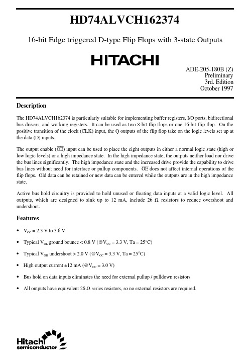
HD74ALVCH16237416-bit Edge triggered D-type Flip Flops with 3-state OutputsADE-205-180B (Z)Preliminary3rd. EditionOctober 1997 DescriptionThe HD74ALVCH162374 is particularly suitable for implementing buffer registers, I/O ports, bidirectional bus drivers, and working registers. It can be used as two 8-bit flip flops or one 16-bit flip flop. On the positive transition of the clock (CLK) input, the Q outputs of the flip flop take on the logic levels set up at the data (D) inputs.The output enable (OE) input can be used to place the eight outputs in either a normal logic state (high or low logic levels) or a high impedance state. In the high impedance state, the outputs neither load nor drive the bus lines significantly. The high impedance state and the increased drive provide the capability to drive bus lines without need for interface or pullup components. OE does not affect internal operations of the flip flops. Old data can be retained or new data can be entered while the outputs are in the high impedance state.Active bus hold circuitry is provided to hold unused or floating data inputs at a valid logic level. All outputs, which are designed to sink up to 12 mA, include 26 Ω resistors to reduce overshoot and undershoot.Features• V CC = 2.3 V to 3.6 V• Typical V OL ground bounce < 0.8 V (@V CC = 3.3 V, Ta = 25°C)• Typical V OH undershoot > 2.0 V (@V CC = 3.3 V, Ta = 25°C)• High output current ±12 mA (@V CC = 3.0 V)• Bus hold on data inputs eliminates the need for external pullup / pulldown resistors• All outputs have equivalent 26 Ω series resistors, so no external resistors are required.HD74ALVCH1623742Function TableInputs Output QOE CLK D L ↑H H L ↑L L L H or L X Q 0 *1HXXZ H : High level L : Low level X : ImmaterialZ : High impedance↑ : Low to high transitionNote: 1.Output level before the indicated steady state input conditions were established.HD74ALVCH162374 Pin Arrangement3HD74ALVCH1623744Absolute Maximum RatingsItemSymbol Ratings Unit ConditionsSupply voltage V CC –0.5 to 4.6V Input voltage *1V I –0.5 to 4.6V Output voltage *1, 2V O –0.5 to V CC +0.5V Input clamp current I IK –50mA V I < 0Output clamp current I OK ±50mA V O < 0 or V O > V CC Continuous output current I O±50mA V O = 0 to V CC V CC , GND current / pin I CC or I GND ±100mA Maximum power dissipation at Ta = 55°C (in still air) *3P T 0.85W TSSOP Storage temperature Tstg–65 to 150°CNotes:Stresses beyond those listed under “absolute maximum ratings” may cause permanent damage to the device. These are stress ratings only, and functional operation of the device at these or any other conditions beyond those indicated under “recommended operating conditions” is not implied. Exposure to absolute maximum rated conditions for extended periods may affect device reliability.1.The input and output negative voltage ratings may be exceeded if the input and output clampcurrent ratings are observed.2.This value is limited to 4.6 V maximum.3.The maximum package power dissipation is calculated using a junction temperature of 150°Cand a board trace length of 750 mils.Recommended Operating ConditionsItemSymbol Min Max Unit ConditionsSupply voltage V CC 2.3 3.6V Input voltage V I 0V CC V Output voltageV O 0V CC V High level output currentI OH—–6mAV CC = 2.3 V —–8V CC = 2.7 V —–12V CC = 3.0 V Low level output currentI OL—6mA V CC = 2.3 V —8V CC = 2.7 V —12V CC = 3.0 V Input transition rise or fall rate ∆t / ∆v 010ns / V Operating temperatureTa–4085°C Note:Unused control inputs must be held high or low to prevent them from floating.HD74ALVCH162374 Logic Diagram5HD74ALVCH1623746Electrical Characteristics (Ta = –40 to 85°C)Item Symbol V CC (V)Min Max Unit Test ConditionsInput voltageV IH 2.3 to 2.7 1.7—V2.7 to3.6 2.0—V IL2.3 to 2.7—0.72.7 to3.6—0.8Output voltageV OHMin to Max V CC –0.2—VI OH = –100 µA2.3 1.9—I OH = –4 mA, V IH = 1.7 V 2.3 1.7—I OH = –6 mA, V IH = 1.7 V3.0 2.4—I OH = –6 mA, V IH = 2.0 V 2.7 2.0—I OH = –8 mA, V IH = 2.0 V 3.02.0—I OH = –12 mA, V IH = 2.0 V V OLMin to Max —0.2I OL = 100 µA2.3—0.4I OL = 4 mA, V IL = 0.7 V 2.3—0.55I OL = 6 mA, V IL = 0.7 V3.0—0.55I OL = 6 mA, V IL = 0.8 V 2.7—0.6I OL = 8 mA, V IL = 0.8 V 3.0—0.8I OL = 12 mA, V IL = 0.8 V Input currentI IN 3.6—±5µA V IN = V CC or GND I IN (hold)2.345—V IN = 0.7 V 2.3–45—V IN = 1.7 V3.075—V IN = 0.8 V 3.0–75—V IN = 2.0 V 3.6—±500V IN = 0 to 3.6 V *1Off state output currentI OZ 3.6—±10µA V OUT = V CC or GND Quiescent supply current I CC3.6—40µA V IN = V CC or GND∆I CC3.0 to 3.6—750µA V IN = one input at (V CC –0.6)V,other inputs at V CC or GND Note:1.This is the bus hold maximum dynamic current required to switch the input from one state toanother.HD74ALVCH1623747Switching Characteristics (Ta = –40 to 85°C)ItemSymbol V CC (V)Min Typ Max Unit FROM (Input)TO(Output)Maximum clock frequency f max2.5±0.2150——MHz2.7150——3.3±0.3150——Propagation delay timet PLH 2.5±0.2 1.0— 5.4nsCLKQt PHL2.7—— 5.43.3±0.3 1.0—4.6Output enable timet ZH 2.5±0.2 1.0— 6.5nsOEQt ZL2.7—— 6.43.3±0.3 1.0— 5.2Output disable timet HZ 2.5±0.2 1.0— 5.6nsOEQt LZ2.7—— 5.03.3±0.3 1.2—4.5Setup timet su2.5±0.2 2.1——ns 2.7 2.2——3.3±0.31.9——Hold timet h2.5±0.20.6——ns 2.70.5——3.3±0.30.5——Pulse widtht w2.5±0.23.3——ns 2.7 3.3——3.3±0.33.3——Input capacitance C IN 3.3— 3.0—pFControl inputs 3.3— 6.0—Data inputsOutput capacitanceC O3.3—7.0—pFHD74ALVCH1623748HD74ALVCH1623749HD74ALVCH16237410HD74ALVCH162374 Package DimensionsUnit : mm11Cautions1.Hitachi neither warrants nor grants licenses of any rights of Hitachi’s or any third party’s patent,copyright, trademark, or other intellectual property rights for information contained in this document.Hitachi bears no responsibility for problems that may arise with third party’s rights, includingintellectual property rights, in connection with use of the information contained in this document.2.Products and product specifications may be subject to change without notice. Confirm that you have received the latest product standards or specifications before final design, purchase or use.3.Hitachi makes every attempt to ensure that its products are of high quality and reliability. However,contact Hitachi’s sales office before using the product in an application that demands especially high quality and reliability or where its failure or malfunction may directly threaten human life or cause risk of bodily injury, such as aerospace, aeronautics, nuclear power, combustion control, transportation,traffic, safety equipment or medical equipment for life support.4.Design your application so that the product is used within the ranges guaranteed by Hitachi particularly for maximum rating, operating supply voltage range, heat radiation characteristics, installationconditions and other characteristics. Hitachi bears no responsibility for failure or damage when used beyond the guaranteed ranges. Even within the guaranteed ranges, consider normally foreseeable failure rates or failure modes in semiconductor devices and employ systemic measures such as fail-safes, so that the equipment incorporating Hitachi product does not cause bodily injury, fire or other consequential damage due to operation of the Hitachi product.5.This product is not designed to be radiation resistant.6.No one is permitted to reproduce or duplicate, in any form, the whole or part of this document without written approval from Hitachi.7.Contact Hitachi’s sales office for any questions regarding this document or Hitachi semiconductor products.Hitachi, Ltd.Semiconductor & Integrated Circuits.Nippon Bldg., 2-6-2, Ohte-machi, Chiyoda-ku, Tokyo 100-0004, Japan Tel: Tokyo (03) 3270-2111 Fax: (03) 3270-5109Copyright ' Hitachi, Ltd., 1999. All rights reserved. Printed in Japan.Hitachi Asia Pte. Ltd.16 Collyer Quay #20-00Hitachi TowerSingapore 049318Tel: 535-2100Fax: 535-1533URLNorthAmerica : http:/Europe : /hel/ecg Asia (Singapore): .sg/grp3/sicd/index.htm Asia (Taiwan): /E/Product/SICD_Frame.htm Asia (HongKong): /eng/bo/grp3/index.htm Japan : http://www.hitachi.co.jp/Sicd/indx.htmHitachi Asia Ltd.Taipei Branch Office3F, Hung Kuo Building. No.167, Tun-Hwa North Road, Taipei (105)Tel: <886> (2) 2718-3666Fax: <886> (2) 2718-8180Hitachi Asia (Hong Kong) Ltd.Group III (Electronic Components)7/F., North Tower, World Finance Centre,Harbour City, Canton Road, Tsim Sha Tsui,Kowloon, Hong Kong Tel: <852> (2) 735 9218Fax: <852> (2) 730 0281 Telex: 40815 HITEC HXHitachi Europe Ltd.Electronic Components Group.Whitebrook ParkLower Cookham Road MaidenheadBerkshire SL6 8YA, United Kingdom Tel: <44> (1628) 585000Fax: <44> (1628) 778322Hitachi Europe GmbHElectronic components Group Dornacher Stra§e 3D-85622 Feldkirchen, Munich GermanyTel: <49> (89) 9 9180-0Fax: <49> (89) 9 29 30 00Hitachi Semiconductor (America) Inc.179 East Tasman Drive,San Jose,CA 95134 Tel: <1> (408) 433-1990Fax: <1>(408) 433-0223For further information write to:。
HD74LV1G14AVS中文资料

Features
• The basic gate function is lined up as hitachi uni logic series. • Supplied on emboss taping for high speed automatic mounting. • Electrical characteristics equivalent to the HD74LV14A Supply voltage range : 1.65 to 5.5 V Operating temperature range : –40 to +85°C • All inputs VIH (Max.) = 5.5 V (@VCC = 0 V to 5.5 V) All outputs VO (Max.) = 5.5 V (@VCC = 0 V) • Output current ±6 mA (@VCC = 3.0 V to 3.6 V), ±12 mA (@VCC = 4.5 V to 5.5 V) • All the logical input has hysteresis voltage for the slow transition.
2
HD74LV1G14A
Function Table
Input A H L H : High level L : Low level Output Y L H
Pin Arrangement
NC
1
5
VCC
IN A
2
GND
3
4
OUT Y
(Top view)
3
ቤተ መጻሕፍቲ ባይዱD74LV1G14A
Absolute Maximum Ratings
HD74LVCC4245A中文资料
Electrical Characteristics (cont)
(Ta = –40 to 85°C)
Item Input current Off state output current Output leak current Quiescent supply current Symbol IIN IOZ IOFF ICCA VCCA (V) 5.5 5.5 0 5.5 5.5 VCCB (V) 3.6 5.5 3.6 5.5 0 OPEN 3.6 5.5 Min Max ±1 ±5 20 80 80 80 Unit Test Conditions µA Control input VI = VCCA or GND µA µA µA VI (CONT) = VIH or VIL, VO = VCCA, VCCB or GND A port, VI/O = 5.5 V, B port, VI/O = 3.6 V An = VCCA or GND, Control input = VCCA B to A, Control input =VCCA or GND Bn = VCCB or GND, IO (A port) = 0 µA A to B, Control input =VCCA or GND An = VCCA or GND, IO (B port) = 0
Output voltage
V
VOLA VOLB
4.5 4.5 4.5 4.5
IOL = 100µA IOL = 24 mA IOL = 100 µA IOL = 12 mA IOL = 24 mA
Rev.1.01 Apr. 13, 2005 page 3 of 8
元器件交易网
74LVC2G66GT资料
9. Recommended operating conditions
Table 6. Symbol VCC VI VSW Tamb ∆t/∆V Recommended operating conditions Parameter supply voltage input voltage switch voltage ambient temperature input transition rise and fall rate VCC = 1.65 V to 2.7 V VCC = 2.7 V to 5.5 V
4. Marking
Table 2. Marking Marking code V66 V66 V66 V66 Type number 74LVC2G66DP 74LVC2G66DC 74LVC2G66GT 74LVC2G66GM
5. Functional diagram
1Y
1Z
1 1 1 X1 2
74LVC2G66_2
© NXP B.V. 2007. All rights reserved.
Product data sheet
Rev. 02 — 28 August 2007
3 of 23
元器件交易网
NXP Semiconductors
74LVC2G66
Bilateral s[1]
Min −0.5 −0.5 −50 [2]
Max +6.5 +6.5 ±50 VCC + 0.5 ±50 100 +150 250
Unit V V mA mA V mA mA mA °C mW
VI < −0.5 V or VI > VCC + 0.5 V VI < −0.5 V or VI > VCC + 0.5 V enable and disable mode VSW > −0.5 V or VSW < VCC + 0.5 V
HD74ALVC16835TEL资料

To all our customersRegarding the change of names mentioned in the document, such as Hitachi Electric and Hitachi XX, to Renesas Technology Corp.The semiconductor operations of Mitsubishi Electric and Hitachi were transferred to Renesas Technology Corporation on April 1st 2003. These operations include microcomputer, logic, analog and discrete devices, and memory chips other than DRAMs (flash memory, SRAMs etc.) Accordingly, although Hitachi, Hitachi, Ltd., Hitachi Semiconductors, and other Hitachi brand names are mentioned in the document, these names have in fact all been changed to Renesas Technology Corp. Thank you for your understanding. Except for our corporate trademark, logo and corporate statement, no changes whatsoever have been made to the contents of the document, and these changes do not constitute any alteration to the contents of the document itself.Renesas Technology Home Page: Renesas Technology Corp.Customer Support Dept.April 1, 2003CautionsKeep safety first in your circuit designs!1. Renesas Technology Corporation puts the maximum effort into making semiconductor products betterand more reliable, but there is always the possibility that trouble may occur with them. Trouble with semiconductors may lead to personal injury, fire or property damage.Remember to give due consideration to safety when making your circuit designs, with appropriate measures such as (i) placement of substitutive, auxiliary circuits, (ii) use of nonflammable material or (iii) prevention against any malfunction or mishap.Notes regarding these materials1. These materials are intended as a reference to assist our customers in the selection of the RenesasTechnology Corporation product best suited to the customer's application; they do not convey any license under any intellectual property rights, or any other rights, belonging to Renesas Technology Corporation or a third party.2. Renesas Technology Corporation assumes no responsibility for any damage, or infringement of anythird-party's rights, originating in the use of any product data, diagrams, charts, programs, algorithms, or circuit application examples contained in these materials.3. All information contained in these materials, including product data, diagrams, charts, programs andalgorithms represents information on products at the time of publication of these materials, and are subject to change by Renesas Technology Corporation without notice due to product improvements or other reasons. It is therefore recommended that customers contact Renesas Technology Corporation or an authorized Renesas Technology Corporation product distributor for the latest product information before purchasing a product listed herein.The information described here may contain technical inaccuracies or typographical errors.Renesas Technology Corporation assumes no responsibility for any damage, liability, or other loss rising from these inaccuracies or errors.Please also pay attention to information published by Renesas Technology Corporation by various means, including the Renesas Technology Corporation Semiconductor home page().4. When using any or all of the information contained in these materials, including product data, diagrams,charts, programs, and algorithms, please be sure to evaluate all information as a total system before making a final decision on the applicability of the information and products. Renesas Technology Corporation assumes no responsibility for any damage, liability or other loss resulting from theinformation contained herein.5. Renesas Technology Corporation semiconductors are not designed or manufactured for use in a deviceor system that is used under circumstances in which human life is potentially at stake. Please contact Renesas Technology Corporation or an authorized Renesas Technology Corporation product distributor when considering the use of a product contained herein for any specific purposes, such as apparatus or systems for transportation, vehicular, medical, aerospace, nuclear, or undersea repeater use.6. The prior written approval of Renesas Technology Corporation is necessary to reprint or reproduce inwhole or in part these materials.7. If these products or technologies are subject to the Japanese export control restrictions, they must beexported under a license from the Japanese government and cannot be imported into a country other than the approved destination.Any diversion or reexport contrary to the export control laws and regulations of Japan and/or thecountry of destination is prohibited.8. Please contact Renesas Technology Corporation for further details on these materials or the productscontained therein.HD74ALVC1683518-bit Universal Bus Driver with 3-state OutputsADE-205-192E (Z)Preliminary6th. EditionJanuary 1999 DescriptionThe HD74ALVC16835 is an 18-bit universal bus driver designed for 2.3 V to 3.6 V Voperation.CCData flow from A to Y is controlled by output enable (OE). The device operates in the transparent mode when the latch enable (LE) input is high. The A data is latched if the clock (CLK) input is held at a high or low logic level. If LE is low, the A data is stored in the latch/flip flop on the low to high transition of the CLK. When OE is high, the outputs are in the high impedance state.To ensure the high impedance state during power up or power down, OE should be tied to Vthrough aCCpullup registor; the minimum value of the registor is determined by the current sinking capability of the driver.Features• Meets “PC SDRAM registered DIMM design support document, Rev. 1.2”• V CC = 2.3 V to 3.6 V• Typical V OL ground bounce < 0.8 V (@V CC = 3.3 V, Ta = 25°C)• Typical V OH undershoot > 2.0 V (@V CC = 3.3 V, Ta = 25°C)• High output current ±24 mA (@V CC = 3.0 V)HD74ALVC16835Function TableInputsOE LE CLK A Output YH X X X ZL H X L LL H X H HL L↑L LL L↑H H*1L L H X Y*2L L L X YH :High levelL :Low levelX :ImmaterialZ :High impedance↑ :Low to high transitionNotes: 1.Output level before the indicated steady-state input conditions were established, provided that CLK was high before LE went low.2.Output level before the indicated steady-state input conditions were established.HD74ALVC16835 Pin ArrangementHD74ALVC16835Absolute Maximum RatingsItem Symbol Ratings Unit Conditions Supply voltage range VCC–0.5 to 4.6VInput voltage range *1VI–0.5 to 4.6VOutput voltage range *1,2VO –0.5 to VCC+0.5VInput clamp current IIK –50mA VI< 0Output clamp current IOK ±50mA VO< 0 or VO> VCCContinuous output current IO ±50mA VO= 0 to VCCVCC , GND current / pin ICCor IGND±100mAMaximum power dissipation at Ta = 55°C (in still air) *3PT1W TSSOPStorage temperature range Tstg–65 to 150°CStresses beyond those listed under “absolute maximum ratings” may cause permanent damage to the device. These are stress ratings only, and functional operation of the device at these or any other conditions beyond those indicated under “recommended operating condition” is not implied. Exposure to absolute-maximum-rated conditions for extended periods may affect device reliability.Notes: 1.The input and output negative-voltage ratings may be exceeded if the input and output clamp current ratings are observed.2.The input and output positive-voltage ratings may be exceeded up to 4.6 V if the input and outputclamp-current ratings are observed.3.The maximum power dissipation is calculated using a junction temperature of 150°C and boardtrace length of 750 mils.Recommended Operating ConditionsItem Symbol Min Max Unit ConditionsSupply voltage VCC2.33.6VInput voltage VI 0VCCVOutput voltage VO 0VCCVHigh-level output current IOH —–12mA VCC= 2.3 V—–12VCC= 2.7 V—–24VCC= 3.0 VLow-level output current IOL —12mA VCC= 2.3 V—12VCC= 2.7 V—24VCC= 3.0 VInput transition rise or fall rate∆t/∆v010ns/V Operating free-air temperature Ta–4085°C Note: Unused or floating control pins must be held high or low.HD74ALVC16835 Logic DiagramHD74ALVC16835Electrical CharacteristicsTa = –40 to 85°CItem Symbol VCC(V)Min Max Unit Test ConditionsInput voltage VIH2.3 to 2.7 1.7—V2.7 to3.6 2.0—VIL2.3 to 2.7—0.7V2.7 to3.6—0.8Output voltage VOH 2.3 to 3.6VCC–0.2—V IOH= –100 µA2.3 2.0—IOH= –6 mA, VIH= 1.7 V2.3 1.7—IOH= –12 mA, VIH= 1.7 V2.7 2.2—IOH= –12 mA, VIH= 2.0 V3.0 2.4—IOH= –12 mA, VIH= 2.0 V3.0 2.0—IOH= –24 mA, VIH= 2.0 VVOL 2.3 to 3.6—0.2V IOL= 100 µA2.3—0.4IOL= 6 mA, VIL= 0.7 V2.3—0.7IOL= 12 mA, VIL= 0.7 V2.7—0.4IOL= 12 mA, VIL= 0.8 V3.0—0.55IOL= 24 mA, VIL= 0.8 VInput current IIN 3.6—±5.0µA VIN= VCCor GNDOff state output current IOZ 3.6—±10µA VOUT= VCCor GNDQuiescent supply current ICC 3.6—40µA VIN= VCCor GND∆ICC 3.0 to 3.6—750µA One input at (VCC–0.6)V,other inputs at VCCor GNDHD74ALVC16835 Switching Characteristics (Ta = –40 to 85°C)(V)Min Typ Max Unit From (Input)To (Output) Item Symbol VCC2.5±0.2150——MHzMaximum clock fmaxfrequency 2.7150——3.3±0.3150——2.5±0.2 1.0— 4.2ns A Y Propagation delay time tPLH2.7—— 4.2tPHL3.3±0.3 1.0— 3.62.5±0.2 1.3— 5.0LE Y2.7—— 4.93.3±0.3 1.3—4.22.5±0.2 1.4— 5.5CLK Y2.7—— 5.23.3±0.3 1.4—4.52.5±0.2 1.4— 5.5ns OE YOutput enable time tZH2.7—— 5.6tZL3.3±0.3 1.1—4.62.5±0.2 1.0— 4.5ns OE YOutput disable time tHZt2.7—— 4.3LZ3.3±0.3 1.3— 3.93.3 3.04.57.0pF Control inputsInput capacitance CIN3.3 3.0 6.09.0Data inputs3.3 3.07.09.0pF Y portsOutput capacitance COHD74ALVC16835Switching Characteristics (Ta = –40 to 85°C) (cont)Item Symbol VCC(V)Min Typ Max Unit From (Input)Setup time tsu2.5±0.2 2.2——ns Data before CLK↑2.7 2.1——3.3±0.3 1.7——2.5±0.2 1.9——Data before LE↓2.7 1.6——CLK “H”3.3±0.3 1.5——2.5±0.2 1.3——Data before LE↓2.7 1.1——CLK “L”3.3±0.3 1.0——Hold time th2.5±0.20.6——ns Data after CLK↑2.70.6——3.3±0.30.7——2.5±0.2 1.4——Data after LE↓2.7 1.7——CLK “H” or “L”3.3±0.3 1.4——Pulse width tw2.5±0.23.3——ns LE “H”2.73.3——3.3±0.3 3.3——2.5±0.23.3——CLK “H” or “L”2.73.3——3.3±0.3 3.3——Switching Characteristics (Ta = 0 to 85°C)Item Symbol VCC(V)Min Typ Max Unit FROM(Input)TO (Output)Propagation CL=0pF*1t PLH, t PHL 3.3±0.1650.9— 2.0ns A Ydelay time CL=50pF 3.3±0.165 1.0— 4.5CL=0pF*1 3.3±0.165 1.5— 3.0CLK YCL=50pF 3.3±0.165 1.7— 4.5CL=50pF t SSO*1, 2 3.3±0.165 1.7— 4.8CLK, A YOutput rise / fall time CL=50pF t TLH, t THL*13.3±0.165 1.0— 2.5volts/nsYNotes: 1.This parameter is characterized but not tested.2.tSSO: Simultaneous switching output time.Operating Characteristics (Ta = 25°C)Item Symbol VCC = 2.5±0.2 V VCC= 3.3±0.3 V Unit Test ConditionsTyp TypPower dissipation Outputs enable Cpd 22.024.5pF CL= 0, f = 10 MHzcapacitance Outputs disable 5.0 6.0 Test CircuitWaveforms – 2IV Characteristics for Register Output (Measured value)Package DimensionsUnit : mmCautions1.Hitachi neither warrants nor grants licenses of any rights of Hitachi’s or any third party’s patent,copyright, trademark, or other intellectual property rights for information contained in this document.Hitachi bears no responsibility for problems that may arise with third party’s rights, includingintellectual property rights, in connection with use of the information contained in this document.2.Products and product specifications may be subject to change without notice. Confirm that you have received the latest product standards or specifications before final design, purchase or use.3.Hitachi makes every attempt to ensure that its products are of high quality and reliability. However,contact Hitachi’s sales office before using the product in an application that demands especially high quality and reliability or where its failure or malfunction may directly threaten human life or cause risk of bodily injury, such as aerospace, aeronautics, nuclear power, combustion control, transportation,traffic, safety equipment or medical equipment for life support.4.Design your application so that the product is used within the ranges guaranteed by Hitachi particularly for maximum rating, operating supply voltage range, heat radiation characteristics, installationconditions and other characteristics. Hitachi bears no responsibility for failure or damage when used beyond the guaranteed ranges. Even within the guaranteed ranges, consider normally foreseeable failure rates or failure modes in semiconductor devices and employ systemic measures such as fail-safes, so that the equipment incorporating Hitachi product does not cause bodily injury, fire or other consequential damage due to operation of the Hitachi product.5.This product is not designed to be radiation resistant.6.No one is permitted to reproduce or duplicate, in any form, the whole or part of this document without written approval from Hitachi.7.Contact Hitachi’s sales office for any questions regarding this document or Hitachi semiconductor products.Semiconductor & IC Div.Nippon Bldg., 2-6-2, Ohte-machi, Chiyoda-ku, Tokyo 100-0004, Japan Tel: Tokyo (03) 3270-2111 Fax: (03) 3270-5109Copyright © Hitachi, Ltd., 1998. All rights reserved. Printed in Japan.Hitachi Asia Pte. Ltd.16 Collyer Quay #20-00Hitachi TowerSingapore 049318Tel: 535-2100Fax: 535-1533URLNorthAmerica : http:/Europe : /hel/ecg Asia (Singapore): .sg/grp3/sicd/index.htm Asia (Taiwan): /E/Product/SICD_Frame.htm Asia (HongKong): /eng/bo/grp3/index.htm Japan : http://www.hitachi.co.jp/Sicd/indx.htmHitachi Asia Ltd.Taipei Branch Office3F, Hung Kuo Building. No.167, Tun-Hwa North Road, Taipei (105)Tel: <886> (2) 2718-3666Fax: <886> (2) 2718-8180Hitachi Asia (Hong Kong) Ltd.Group III (Electronic Components)7/F., North Tower, World Finance Centre,Harbour City, Canton Road, Tsim Sha Tsui,Kowloon, Hong Kong Tel: <852> (2) 735 9218Fax: <852> (2) 730 0281 Telex: 40815 HITEC HXHitachi Europe Ltd.Electronic Components Group.Whitebrook ParkLower Cookham Road MaidenheadBerkshire SL6 8YA, United Kingdom Tel: <44> (1628) 585000Fax: <44> (1628) 778322Hitachi Europe GmbHElectronic components Group Dornacher Straße 3D-85622 Feldkirchen, Munich GermanyTel: <49> (89) 9 9180-0Fax: <49> (89) 9 29 30 00Hitachi Semiconductor (America) Inc.2000 Sierra Point Parkway Brisbane, CA 94005-1897Tel: <1> (800) 285-1601Fax: <1> (303) 297-0447For further information write to:。
74系列中lvclvhcls等有什么区别

74系列中lvclvhcls等有什么区别74系列中lvc lv hc ls等有什么区别ABT高级双极CMOS技术ABTE/ETL高级双极CMOS技术增强收发逻辑AC/ACT高级CMOS逻辑AHC/AHCT高级高速CMOS逻辑ALB高级低电压BiCMOSALS高级低功耗肖特基逻辑ALVC高级低电压CMOS技术ALVT高级低电压BiCMOS技术AS高级肖特基逻辑AUC高级极低电压CMOS逻辑AUP高级极低功耗CMOS逻辑AVC高级很低电压CMOS逻辑BCT双极CMOS技术CB3Q 2.5V、3.3V低电压高带宽总线交换纵横逻辑CB3T 2.5V、3.3V低电压晶体管总线交换纵横逻辑CBT纵横技术CBT-C有2V下冲保护的5V总线交换纵横逻辑CBTLV低电压纵横技术逻辑CD4000CMOS逻辑4000系列F快速逻辑FB基底电极收发逻辑FCT高速CMOS技术GTL电子?收发逻辑GTLP电子?收发逻辑+HC/HCT高速CMOS逻辑HSTL高速收发逻辑LS低功耗肖特基逻辑LV低电压LV-A低电压CMOS技术LV-AT低电压CMOS技术并兼容TTL电平LVC低电压CMOS技术LVT低电压BiCMOS技术S肖特基逻辑SSTL抽头级联逻辑SSTU抽头级联极低电压逻辑SSTV/SSTVF抽头级联低电压逻辑TVC平移电压箝位逻辑这些逻辑电平对应的英文含义如下:S-Schottky LogicLS-Low-Power Schottky LogicCD4000-CMOS Logic4000AS-Advanced Schottky Logic74F-Fast LogicALS-Advanced Low-Power Schottky LogicHC/HCT-High-Speed CMOS LogicBCT-BiCMOS TechnologyAC/ACT-Advanced CMOS LogicFCT-Fast CMOS TechnologyABT-Advanced BiCMOS TechnologyLVT-Low-Voltage BiCMOS TechnologyLVC-Low Voltage CMOS TechnologyLV-Low-VoltageCBT-Crossbar TechnologyALVC-Advanced Low-Voltage CMOS Technology AHC/AHCT-Advanced High-Speed CMOSCBTLV-Low-Voltage Crossbar TechnologyALVT-Advanced Low-Voltage BiCMOS Technology AVC-Advanced Very-Low-Voltage CMOS Logic。
74LVC2G07中文资料
Product specification
Buffers with open-drain outputs
FEATURES • Wide supply voltage range from 1.65 V to 5.5 V • 5 V tolerant input/output for interfacing with 5 V logic • High noise immunity • Complies with JEDEC standard: – JESD8-7 (1.65 V to 1.95 V) – JESD8-5 (2.3 V to 2.7 V) – JESD8B/JESD36 (2.7 V to 3.6 V). • −24 mA output drive (VCC = 3.0 V) • CMOS low power consumption • Latch-up performance exceeds 250 mA • Direct interface with TTL levels • Inputs accept voltages up to 5 V • Multiple package options • ESD protection: – HBM EIA/JESD22-A114-B exceeds 2000 V – MM EIA/JESD22-A115-A exceeds 200 V. • Specified from −40 °C to +85 °C and −40 °C to +125 °C. QUICK REFERENCE DATA GND = 0 V; Tamb = 25 °C. SYMBOL tPLZ/tPZL PARAMETER CONDITIONS DESCRIPTION
74LVC2G07
HD74ALVC1G04VS中文资料

Item Propagation delay time
Rev.0, Jun. 2001, page 6 of 10
HD74ALVC1G04
Operating Characteristics
(Ta = 25°C)
Item Power dissipation capacitance Symbol CPD VCC (V) 1.5 1.8 2.5 3.3 Min Typ 9.5 9.5 10.0 10.5 Max Unit pF Test conditions f = 10 MHz
Rev.0, Jun. 2001, page 4 of 10
HD74ALVC1G04
Electrical Characteristics
(Ta = −40 to 85°C)
Item Input voltage Symbol VIH VCC (V) 1.2 1.4 to 1.6 1.65 to 1.95 2.3 to 2.7 3.0 to 3.6 VIL 1.2 1.4 to 1.6 1.65 to 1.95 2.3 to 2.7 3.0 to 3.6 Output voltage VOH Min to Max 1.2 1.4 1.65 2.3 3.0 VOL Min to Max 1.2 1.4 1.65 2.3 3.0 Input current Quiescent supply current Output leakage current Input capacitance IIN ICC IOFF CIN 3.6 3.6 0 3.3
•
VCC = 1.8±0.15 V
Symbol tPLH tPHL Min 1.5 Typ Max 5.0 Unit ns Test conditions CL = 30 pF FROM (Input) A TO (Output) Y
74ALVC02中文资料
INTEGRATED CIRCUITS
DATA SHEET
74ALVC02 Quad 2-input NOR gate
Product specification Supersedes data of 2003 Feb 05 2003 Jul 14
元器件交易网
CODE SOT108-1 SOT402-1 SOT762-1
OUTPUT nB L H L H nY H L L L
1Y 1A 1B 2Y 2A 2B GND
1 2 3 4 5 6 7
MNA214
14 VCC 13 4Y 12 4B
02
11 4A 10 3Y 9 3B
8 3A
Fig.1 Pin configuration SO14 and TSSOP14.
MNA215
1A 1B 2Y 2A 2B
2 3 4 5 6 7 Top view GND 8 3A
handbook, halfpage
A Y
GND(1)
11 10 9
MNA951
(1) (1) The die substrate is attached to this pad using conductive die attach material. It can not be used as a supply pin or input.
2003 Jul 14
5
元器件交易网
Philips Semiconductors
Product specification
Quad 2-input NOR gate
DC CHARACTERISTICS At recommended operating conditions; voltages are referenced to GND (ground = 0 V). TEST CONDITIONS SYMBOL PARAMETER OTHER Tamb = −40 to +85 °C VIH HIGH-level input voltage 1.65 to 1.95 0.65 × VCC − 2.3 to 2.7 2.7 to 3.6 VIL LOW-level input voltage 2.3 to 2.7 2.7 to 3.6 VOL LOW-level output voltage VI = VIH or VIL IO = 100 µA IO = 6 mA IO = 12 mA IO = 18 mA IO = 12 mA IO = 18 mA IO = 24 mA VOH HIGH-level output voltage VI = VIH or VIL IO = −100 µA IO = −6 mA IO = −12 mA IO = −18 mA IO = −12 mA IO = −18 mA IO = −24 mA ILI Ioff ICC ∆ICC input leakage current VI = 3.6 V or GND 1.65 to 3.6 1.65 2.3 2.3 2.7 3.0 3.0 3.6 0.0 3.6 3.0 to 3.6 VCC − 0.2 1.25 1.8 1.7 2.2 2.4 2.2 − − − − − 1.51 2.10 2.01 2.53 2.76 2.68 ±0.1 ±0.1 0.2 5 1.65 to 3.6 1.65 2.3 2.3 2.7 3.0 3.0 − − − − − − − − 0.11 0.17 0.25 0.16 0.23 0.30 1.7 2 − − − − − − − VCC (V) MIN. TYP.(1)
HD74ALVCH16260T中文资料

HD74ALVCH1626012-bit to 24-bit Multiplexed D-type Latches with 3-state OutputsADE-205-135B (Z)3rd. EditionDecember 1999 DescriptionThe HD74ALVCH16260 is a 12-bit to 24-bit multiplexed D-type latch used in applications where two separate data paths must be multiplexed onto, or demultiplexed from, a single data path. Typical applications include multiplexing and / or demultiplexing of address and data information in microprocessor or bus interface applications. This device is also useful in memory interleaving applications. Three 12-bit I / O ports (A1-A12, 1B1-1B12, and 2B1-2B12) are available for address and / or data transfer. The output enable (OE1B, OE2B, and OEA) inputs control the bus transceiver functions. The OE1B and OE2B control signals also allow bank control in the A-to-B direction. Address and / or data information can be stored using the internal storage latches. The latch enable (LE1B, LE2B, LEA1B, and LEA2B) inputs are used to control data storage. When the latch enable input is high, the latch is transparent. When the latch enable input goes low, the data present at the inputs is latched and remains latched until the latch enable input is returned high. Active bus hold circuitry is provided to hold unused or floating data inputs at a valid logic level.Features• V CC = 2.3 V to 3.6 V• Typical V OL ground bounce < 0.8 V (@V CC = 3.3 V, Ta = 25°C)• Typical V OH undershoot > 2.0 V (@V CC = 3.3 V, Ta = 25°C)• High output current ±24 mA (@V CC = 3.0 V)• Bus hold on data inputs eliminates the need for external pullup / pulldown resistorsHD74ALVCH162602Function TableInputs Output A1B 2B SEL LE1B LE2B OEA H X H H X L H L X H H X L L X X H L X L A 0 *1X H L X H L H X L L X H L L X X L X L L A 0 *1XXXXXHZ B-to-A (OEB = H)Inputs Outputs A LEA1B LEA2B OE1B OE2B 1B 2B H H H L L H H L H H L L L L H H L L L H 2B 0 *1L H L L L L 2B 0 *1H L H L L 1B 0 *1H L L H L L 1B 0 *1L X L L L L 1B 0 *12B 0 *1X X X H H Z Z X X X L H Active Z X X X H L Z Active XXXLLActiveActiveA-to-B (OEA = H)H : High level L : Low level X : ImmaterialZ : High impedanceNote: 1.Output level before the indicated steady state input conditions were established.HD74ALVCH16260 Pin Arrangement3HD74ALVCH162604Absolute Maximum RatingsItemSymbol Ratings Unit ConditionsSupply voltage V CC –0.5 to 4.6V Input voltage *1, 2V I –0.5 to 4.6VExcept I/O ports –0.5 to V CC +0.5I/O ports Output voltage *1, 2V O –0.5 to V CC +0.5V Input clamp current I IK –50mA V I < 0Output clamp current I OK ±50mA V O < 0 or V O > V CC Continuous output current I O±50mA V O = 0 to V CCV CC , GND current / pin I CC or I GND ±100mA Maximum power dissipation at Ta = 55°C (in still air) *3P T 1W TSSOP Storage temperature Tstg–65 to 150°CNotes:Stresses beyond those listed under “absolute maximum ratings” may cause permanent damage to the device. These are stress ratings only, and functional operation of the device at these or any other conditions beyond those indicated under “recommended operating conditions” is not implied. Exposure to absolute maximum rated conditions for extended periods may affect device reliability.1.The input and output negative voltage ratings may be exceeded if the input and output clampcurrent ratings are observed.2.This value is limited to 4.6 V maximum.3.The maximum package power dissipation is calculated using a junction temperature of 150°Cand a board trace length of 750 mils.Recommended Operating ConditionsItemSymbol Min Max Unit ConditionsSupply voltage V CC 2.3 3.6V Input voltage V I 0V CC V Output voltageV O 0V CC V High level output currentI OH—–12mAV CC = 2.3 V —–12V CC = 2.7 V —–24V CC = 3.0 V Low level output currentI OL—12mA V CC = 2.3 V —12V CC = 2.7 V —24V CC = 3.0 V Input transition rise or fall rate ∆t / ∆v 010ns / V Operating temperatureTa–4085°C Note:Unused control inputs must be held high or low to prevent them from floating.HD74ALVCH16260 Logic Diagram5HD74ALVCH162606Electrical Characteristics (Ta = –40 to 85°C)Item Symbol V CC (V) *1Min Max Unit Test ConditionsInput voltageV IH 2.3 to 2.7 1.7—V2.7 to3.6 2.0—V IL2.3 to 2.7—0.72.7 to3.6—0.8Output voltageV OHMin to Max V CC –0.2—VI OH = –100 µA2.3 2.0—I OH = –6 mA, V IH = 1.7 V 2.3 1.7—I OH = –12 mA, V IH = 1.7 V 2.7 2.2—I OH = –12 mA, V IH = 2.0 V3.0 2.4—I OH = –12 mA, V IH = 2.0 V 3.02.0—I OH = –24 mA, V IH = 2.0 V V OLMin to Max —0.2I OL = 100 µA2.3—0.4I OL = 6 mA, V IL = 0.7 V 2.3—0.7I OL = 12 mA, V IL = 0.7 V 2.7—0.4I OL = 12 mA, V IL = 0.8 V3.0—0.55I OL = 24 mA, V IL = 0.8 V Input currentI IN 3.6—±5µA V IN = V CC or GND I IN (hold)2.345—V IN = 0.7 V 2.3–45—V IN = 1.7 V3.075—V IN = 0.8 V 3.0–75—V IN = 2.0 V 3.6—±500V IN = 0 to 3.6 V Off state output current *2I OZ 3.6—±10µA V OUT = V CC or GND Quiescent supply current I CC3.6—40µA V IN = V CC or GND∆I CC3.0 to 3.6—750µA V IN = one input at (V CC –0.6) V,other inputs at V CC or GND Notes: 1.For conditions shown as Min or Max, use the appropriate values under recommended operatingconditions.2.For I/O ports, the parameter I OZ includes the input leakage current.HD74ALVCH162607Switching Characteristics (Ta = –40 to 85°C)ItemSymbol V CC (V)Min Typ Max Unit FROM (Input)TO(Output)Maximum clock frequency f max2.5±0.2150——MHz2.7150——3.3±0.3150——Propagation delay timet PLH 2.5±0.2 1.2— 5.6nsA or BB or At PHL2.7—— 5.13.3±0.3 1.2—4.32.5±0.2 1.0— 6.2LEA or B2.7—— 5.23.3±0.3 1.0—4.42.5±0.2 1.2— 6.9SELA2.7—— 6.63.3±0.31.1— 5.6Output enable timet ZH 2.5±0.2 1.0— 6.7nsOEA or Bt ZL2.7—— 6.43.3±0.3 1.0— 5.4Output disable timet HZ 2.5±0.2 1.7— 5.7nsOEA or Bt LZ2.7—— 5.03.3±0.3 1.3—4.6Setup timet su2.5±0.2 1.4——ns 2.7 1.1——3.3±0.31.1——Hold timet h2.5±0.2 1.6——ns 2.7 1.9——3.3±0.31.5——Pulse widtht w2.5±0.23.3——ns 2.7 3.3——3.3±0.33.3——Input capacitance C IN 3.3— 3.5—pF Control inputs Output capacitanceC IN / O3.3—9.0—pFA orB portsHD74ALVCH162608HD74ALVCH162609HD74ALVCH1626010HD74ALVCH16260 Package DimensionsUnit : mm11HD74ALVCH1626012Cautions1.Hitachi neither warrants nor grants licenses of any rights of Hitachi’s or any third party’s patent,copyright, trademark, or other intellectual property rights for information contained in this document.Hitachi bears no responsibility for problems that may arise with third party’s rights, including intellectual property rights, in connection with use of the information contained in this document.2.Products and product specifications may be subject to change without notice. Confirm that you have received the latest product standards or specifications before final design, purchase or use.3.Hitachi makes every attempt to ensure that its products are of high quality and reliability. However,contact Hitachi’s sales office before using the product in an application that demands especially high quality and reliability or where its failure or malfunction may directly threaten human life or cause risk of bodily injury, such as aerospace, aeronautics, nuclear power, combustion control, transportation,traffic, safety equipment or medical equipment for life support.4.Design your application so that the product is used within the ranges guaranteed by Hitachi particularly for maximum rating, operating supply voltage range, heat radiation characteristics, installationconditions and other characteristics. Hitachi bears no responsibility for failure or damage when used beyond the guaranteed ranges. Even within the guaranteed ranges, consider normally foreseeable failure rates or failure modes in semiconductor devices and employ systemic measures such as fail-safes, so that the equipment incorporating Hitachi product does not cause bodily injury, fire or other consequential damage due to operation of the Hitachi product.5.This product is not designed to be radiation resistant.6.No one is permitted to reproduce or duplicate, in any form, the whole or part of this document without written approval from Hitachi.7.Contact Hitachi’s sales office for any questions regarding this document or Hitachi semiconductor products.Hitachi, Ltd.Semiconductor & Integrated Circuits.Nippon Bldg., 2-6-2, Ohte-machi, Chiyoda-ku, Tokyo 100-0004, Japan Tel: Tokyo (03) 3270-2111 Fax: (03) 3270-5109Copyright ' Hitachi, Ltd., 1999. All rights reserved. Printed in Japan.Hitachi Asia Pte. Ltd.16 Collyer Quay #20-00Hitachi TowerSingapore 049318Tel: 535-2100Fax: 535-1533URLNorthAmerica : http:/Europe : /hel/ecg Asia (Singapore): .sg/grp3/sicd/index.htm Asia (Taiwan): /E/Product/SICD_Frame.htm Asia (HongKong): /eng/bo/grp3/index.htm Japan : http://www.hitachi.co.jp/Sicd/index.htmHitachi Asia Ltd.Taipei Branch Office3F, Hung Kuo Building. No.167, Tun-Hwa North Road, Taipei (105)Tel: <886> (2) 2718-3666Fax: <886> (2) 2718-8180Hitachi Asia (Hong Kong) Ltd.Group III (Electronic Components)7/F., North Tower, World Finance Centre,Harbour City, Canton Road, Tsim Sha Tsui,Kowloon, Hong Kong Tel: <852> (2) 735 9218Fax: <852> (2) 730 0281 Telex: 40815 HITEC HXHitachi Europe Ltd.Electronic Components Group.Whitebrook ParkLower Cookham Road MaidenheadBerkshire SL6 8YA, United Kingdom Tel: <44> (1628) 585000Fax: <44> (1628) 778322Hitachi Europe GmbHElectronic components Group Dornacher Stra§e 3D-85622 Feldkirchen, Munich GermanyTel: <49> (89) 9 9180-0Fax: <49> (89) 9 29 30 00Hitachi Semiconductor (America) Inc.179 East Tasman Drive,San Jose,CA 95134 Tel: <1> (408) 433-1990Fax: <1>(408) 433-0223For further information write to:。
HD74LVC125A资料
HD74LVC125AQuad. Bus Buffer Gates with 3-state OutputsADE-205-108B(Z)3rd EditionDecember 1996 DescriptionThe HD74LVC125A has four bus buffer gates in a 14 pin package. The device require the three state control input C to be taken high to put the output into the high impedance condition, whereas the device requires the control input to be low to put the output into high impedance. Low voltage and high speed operation is suitable at the battery drive product (note type personal computer) and low power consumption extends the life of a battery for long time operation.Features• V CC = 2.0 V to 5.5 V• All inputs V IH (Max.) = 5.5 V (@V CC = 0 V to 5.5 V)• All outputs V OUT (Max.) = 5.5 V (@V CC = 0 V or output off state)• Typical V OL ground bounce < 0.8 V (@V CC = 3.3 V, Ta = 25°C)• Typical V OH undershoot > 2.0 V (@V CC = 3.3 V, Ta = 25°C)• High output current ±24 mA (@V CC = 3.0 V to 5.5 V)Function TableInputsC A Outputs YH X ZL L LL H HH :High levelL :Low levelX :ImmaterialZ :High impedanceHD74LVC125A2Pin ArrangementAbsolute Maximum RatingsItemSymbol Ratings Unit ConditionsSupply voltage V CC –0.5 to 6.0V Input diode current I IK –50mA V I = –0.5 V Input voltage V I –0.5 to 6.0V Output diode current I OK –50mA V O = –0.5 V 50mA V O = V CC +0.5 V Output voltage V O –0.5 to V CC +0.5V Output "H" or "L"–0.5 to 6.0V Output "Z" or V CC :OFF Output current I O±50mA V CC , GND current / pin I CC or I GND 100mA Storage temperatureTstg–65 to +150°CNote:The absolute maximum ratings are values which must not individually be exceeded, and furthermore,no two of which may be realized at the same time.HD74LVC125A3Recommended Operating ConditionsItemSymbol Ratings Unit Conditions Supply voltage V CC 1.5 to 5.5V Data hold 2.0 to 5.5V At operation Input / output voltageV I 0 to 5.5V C, AV O0 to V CC V Output "H" or "L"0 to 5.5V Output "Z" or V CC :OFFOperating temperature Ta –40 to 85°C Output currentI OH –12mA V CC = 2.7 V –24*2mA V CC = 3.0 V to 5.5 V I OL12mA V CC = 2.7 V 24*2mA V CC = 3.0 V to 5.5 V Input rise / fall time *1t r , t f10ns/VNotes: 1.This item guarantees maximum limit when one input switches.Waveform : Refer to test circuit of switching characteristics.2.duty cycle ≤ 50%HD74LVC125A4Electrical CharacteristicsTa = –40 to 85°CItem Symbol V CC (V)MinMax Unit Test ConditionsInput voltageV IH 2.7 to 3.62.0—V 4.5 to 5.5V CC ×0.7—V V IL2.7 to3.6—0.8V 4.5 to 5.5—V CC ×0.3V Output voltageV OH2.7 to 5.5V CC –0.2—V I OH = –100 µA 2.7 2.2—V I OH = –12 mA 3.0 2.4—V 3.0 2.2—V I OH = –24 mA 4.53.8—V V OL2.7 to 5.5—0.2V I OL = 100 µA 2.7—0.4V I OL = 12 mA 3.0—0.55V I OL = 24 mA 4.5—0.55V Input currentI IN 0 to 5.5—±5.0µA V IN = 5.5 V CC GND Off state output currentI IOZ2.7 to 5.5—±5.0µA V IN = V CC , GND V OUT = 5.5 V or GNDOutput leak currentI OFF—20µA V IN / V OUT = 5.5 V Quiescent supply current I CC2.7 to3.6—±10µA V IN / V OUT = 3.6 to 5.5 V 2.7 to 5.5—10µA V IN = V CC or GND∆I CC3.0 to 3.6—500µAV IN = one input at (V CC –0.6) V,other inputs at V CC or GNDHD74LVC125A5Switching CharacteristicsTa = –40 to 85°CItemSymbol V CC (V)Min Typ Max Unit From (Input)To (Output)Propagation delay timet PLH 2.7—— 6.5ns AYt PHL3.3±0.3 1.5— 6.0ns 5.0±0.5—— 5.0ns Output enable timet ZH 2.7——8.0ns CYt ZL3.3±0.3 1.5—7.0ns 5.0±0.5—— 6.0ns Output disable timet HZ 2.7—— 6.5ns CYt LZ3.3±0.3 1.5— 5.5ns 5.0±0.5——4.5ns Between output pins skew *1t OSLH2.7———ns t OSHL3.3±0.3—— 1.0ns 5.0±0.5—— 1.0ns Input capacitance C IN 2.7— 3.0—pF Output capacitance C O2.7—15.0—pFNote:1.This parameter is characterized but not tested.tos LH = | t PLHm - t PLHn |, tos HL = | t PHLm - t PHLn |HD74LVC125A Test Circuit6HD74LVC125A Waveforms – 1Waveforms – 27Hitachi Code JEDEC EIAJWeight (reference value)TTP-14D ——0.05 gUnit: mm*Dimension including the plating thicknessBase material dimension元器件交易网Cautions1.Hitachi neither warrants nor grants licenses of any rights of Hitachi’s or any third party’s patent,copyright, trademark, or other intellectual property rights for information contained in this document.Hitachi bears no responsibility for problems that may arise with third party’s rights, includingintellectual property rights, in connection with use of the information contained in this document.2.Products and product specifications may be subject to change without notice. Confirm that you have received the latest product standards or specifications before final design, purchase or use.3.Hitachi makes every attempt to ensure that its products are of high quality and reliability. However,contact Hitachi’s sales office before using the product in an application that demands especially high quality and reliability or where its failure or malfunction may directly threaten human life or cause risk of bodily injury, such as aerospace, aeronautics, nuclear power, combustion control, transportation,traffic, safety equipment or medical equipment for life support.4.Design your application so that the product is used within the ranges guaranteed by Hitachi particularly for maximum rating, operating supply voltage range, heat radiation characteristics, installationconditions and other characteristics. Hitachi bears no responsibility for failure or damage when used beyond the guaranteed ranges. Even within the guaranteed ranges, consider normally foreseeable failure rates or failure modes in semiconductor devices and employ systemic measures such as fail-safes, so that the equipment incorporating Hitachi product does not cause bodily injury, fire or other consequential damage due to operation of the Hitachi product.5.This product is not designed to be radiation resistant.6.No one is permitted to reproduce or duplicate, in any form, the whole or part of this document without written approval from Hitachi.7.Contact Hitachi’s sales office for any questions regarding this document or Hitachi semiconductor products.Hitachi, Ltd.Semiconductor & Integrated Circuits.Nippon Bldg., 2-6-2, Ohte-machi, Chiyoda-ku, Tokyo 100-0004, Japan Tel: Tokyo (03) 3270-2111 Fax: (03) 3270-5109Copyright ' Hitachi, Ltd., 1999. All rights reserved. Printed in Japan.Hitachi Asia Pte. Ltd.16 Collyer Quay #20-00Hitachi TowerSingapore 049318Tel: 535-2100Fax: 535-1533URLNorthAmerica : http:/Europe : /hel/ecg Asia (Singapore): .sg/grp3/sicd/index.htm Asia (Taiwan): /E/Product/SICD_Frame.htm Asia (HongKong): /eng/bo/grp3/index.htm Japan : http://www.hitachi.co.jp/Sicd/indx.htmHitachi Asia Ltd.Taipei Branch Office3F, Hung Kuo Building. No.167, Tun-Hwa North Road, Taipei (105)Tel: <886> (2) 2718-3666Fax: <886> (2) 2718-8180Hitachi Asia (Hong Kong) Ltd.Group III (Electronic Components)7/F., North Tower, World Finance Centre,Harbour City, Canton Road, Tsim Sha Tsui,Kowloon, Hong Kong Tel: <852> (2) 735 9218Fax: <852> (2) 730 0281 Telex: 40815 HITEC HXHitachi Europe Ltd.Electronic Components Group.Whitebrook ParkLower Cookham Road MaidenheadBerkshire SL6 8YA, United Kingdom Tel: <44> (1628) 585000Fax: <44> (1628) 778322Hitachi Europe GmbHElectronic components Group Dornacher Stra§e 3D-85622 Feldkirchen, Munich GermanyTel: <49> (89) 9 9180-0Fax: <49> (89) 9 29 30 00Hitachi Semiconductor (America) Inc.179 East Tasman Drive,San Jose,CA 95134 Tel: <1> (408) 433-1990Fax: <1>(408) 433-0223For further information write to:。
HD74LV1G04AVSE中文资料

HD74LV1G04AInverterREJ03D0064-0800Rev.8.00 Mar 21, 2008DescriptionThe HD74LV1G04A has an inverter in a 5 pin package. Low voltage and high-speed operation is suitable for the battery powered products (e.g., notebook computers), and the low power consumption extends the battery life.Features• The basic gate function is lined up as Renesas uni logic series. • Supplied on emboss taping for high-speed automatic mounting. • Electrical characteristics equivalent to the HD74LV04A Supply voltage range : 1.65 to 5.5 VOperating temperature range : –40 to +85°C• All inputs V IH (Max.) = 5.5 V (@V CC = 0 V to 5.5 V) All outputs V O (Max.) = 5.5 V (@V CC = 0 V)• Output current ±6 mA (@V CC = 3.0 V to 3.6 V), ±12 mA (@V CC = 4.5 V to 5.5 V) • All the logical input has hysteresis voltage for the slow transition. • Ordering InformationPart NamePackage TypePackage Code (Previous Code) Package AbbreviationTaping Abbreviation(Quantity) HD74LV1G04ACME CMPAK–5 pinPTSP0005ZC-A(CMPAK-5V) CM E (3000 pcs/reel) HD74LV1G04AVSE VSON–5 pinPUSN0005KA-A(TNP-5DV)VSE (3000 pcs/reel)Note: Please consult the sales office for the above package availability.Outline and Article IndicationOutline and Article IndicationFunction TableInput A Output YH LL H H : High levelL : Low levelPin ArrangementAbsolute Maximum RatingsItem Symbol Ratings Unit Test ConditionsSupply voltage range V CC –0.5 to 7.0 VInput voltage range *1V I –0.5 to 7.0 V–0.5 to V CC + 0.5 Output : H or LOutput voltage range *1, 2 V O –0.5 to 7.0 VV CC : OFFInput clamp current I IK –20 mA V I < 0 Output clamp current I OK ±50 mA V O < 0 or V O > V CC Continuous output current I O ±25 mA V O = 0 to V CC Continuous current through V CC or GNDI CC or I GND ±50 mAMaximum power dissipationat Ta = 25°C (in still air) *3P T 200 mW Storage temperature Tstg–65 to 150°CNotes: The absolute maximum ratings are values, which must not individually be exceeded, and furthermore no twoof which may be realized at the same time.1. The input and output voltage ratings may be exceeded if the input and output clamp-current ratings areobserved.2. This value is limited to 5.5 V maximum.3. The maximum package power dissipation was calculated using a junction temperature of 150°C.Recommended Operating ConditionsItem Symbol Min Max Unit ConditionsSupply voltage range V CC 1.65 5.5 V Input voltage range V I 0 5.5 V Output voltage range V O 0 V CC V— 1 V CC = 1.65 to 1.95 V — 2 V CC = 2.3 to 2.7 V— 6 V CC = 3.0 to 3.6 V I OL— 12 V CC = 4.5 to 5.5 V— –1 V CC = 1.65 to 1.95 V — –2 V CC = 2.3 to 2.7 V— –6 V CC = 3.0 to 3.6 V Output current I OH— –12 mAV CC = 4.5 to 5.5 V 0 300 V CC = 1.65 to 1.95 V 0 200 V CC = 2.3 to 2.7 V0 100 V CC = 3.0 to 3.6 V Input transition rise or fall rate ∆t / ∆v 0 20 ns / VV CC = 4.5 to 5.5 V Operating free-air temperatureT a –40 85 °CNote: Unused or floating inputs must be held high or low.• Ta = –40 to 85°CItem Symbol V CC (V) * Min Typ Max Unit Test condition1.65 to 1.95 V CC ×0.75 — —2.3 to 2.7 V CC ×0.7 — —3.0 to 3.6 V CC ×0.7 — — V IH4.5 to5.5 V CC ×0.7 — —1.65 to 1.95 — — V CC ×0.252.3 to 2.7 — — V CC ×0.33.0 to 3.6 — — V CC ×0.3 Input voltage V IL4.5 to5.5 — — V CC ×0.3 V1.8 — 0.25 —2.5 — 0.30 —3.3 — 0.35 —Hysteresis voltage V H 5.0 — 0.45 — V V T + – V T –Min to Max V CC –0.1 — — I OH = –50 µA1.65 1.4 — — I OH = –1 mA2.3 2.0 — —I OH = –2 mA 3.0 2.48 — —I OH = –6 mA V OH4.5 3.8 — —I OH = –12 mAMin to Max — — 0.1I OL = 50 µA 1.65 — — 0.3 I OL = 1 mA 2.3 — — 0.4 I OL = 2 mA 3.0 — — 0.44I OL = 6 mAOutput voltageV OL4.5 — — 0.55 VI OL = 12 mA Input current I IN0 to 5.5 — — ±1 µA V IN = 5.5 V or GNDQuiescent supply current I CC 5.5 — — 10 µAV IN = V CC or GND,I O = 0Output leakage currentI OFF 0 — — 5 µA V IN or V O = 0 to 5.5 V Input capacitanceC IN 3.3 — 3.0 — pF V IN = V CC or GNDNote: For conditions shown as Min or Max, use the appropriate values under recommended operating conditions.• V CC = 1.8 ± 0.15 VTa = 25°C Ta = –40 to 85°CItem Symbol Min Typ Max Min Max UnitTestConditions FROM (Input) TO (Output)— 12.6 22.0 1.0 24.0 C L = 15 pF Propagation delay time t PLHt PHL — 19.7 33.0 1.0 36.0 nsC L = 50 pFAY• V CC = 2.5 ± 0.2 VTa = 25°C Ta = –40 to 85°CItem Symbol Min Typ Max Min Max UnitTestConditions FROM (Input) TO (Output)— 7.0 11.7 1.0 14.0 C L = 15 pF Propagation delay time t PLHt PHL — 10.5 15.5 1.0 18.0 nsC L = 50 pFAY• V CC = 3.3 ± 0.3 VTa = 25°C Ta = –40 to 85°CItem Symbol Min Typ Max Min Max UnitTestConditions FROM (Input) TO (Output)— 5.0 7.1 1.0 8.5 C L = 15 pF Propagation delay time t PLHt PHL — 7.5 10.6 1.0 12.0 nsC L = 50 pFAY• V CC = 5.0 ± 0.5 VTa = 25°C Ta = –40 to 85°CItem Symbol Min Typ Max Min Max UnitTestConditions FROM (Input) TO (Output)— 3.8 5.5 1.0 6.5C L = 15 pF Propagation delay time t PLH t PHL— 5.3 7.5 1.0 8.5nsC L = 50 pFAYOperating Characteristics• C L = 50 pFTa = 25°CItem Symbol V CC (V)Min Typ MaxUnit Test Conditions3.3 — 8.5 —Power dissipationcapacitanceC PD5.0 — 10.0 —pFf = 10 MHzTest CircuitWaveformsPackage DimensionsRefer to "/en/network " for the latest and detailed information.Renesas Technology America, Inc.450 Holger Way, San Jose, CA 95134-1368, U.S.A Tel: <1> (408) 382-7500, Fax: <1> (408) 382-7501Renesas Technology Europe LimitedDukes Meadow, Millboard Road, Bourne End, Buckinghamshire, SL8 5FH, U.K.Tel: <44> (1628) 585-100, Fax: <44> (1628) 585-900Renesas Technology (Shanghai) Co., Ltd.Unit 204, 205, AZIACenter, No.1233 Lujiazui Ring Rd, Pudong District, Shanghai, China 200120Tel: <86> (21) 5877-1818, Fax: <86> (21) 6887-7858/7898Renesas Technology Hong Kong Ltd.7th Floor, North Tower, World Finance Centre, Harbour City, Canton Road, Tsimshatsui, Kowloon, Hong Kong Tel: <852> 2265-6688, Fax: <852> 2377-3473Renesas Technology Taiwan Co., Ltd.10th Floor, No.99, Fushing North Road, Taipei, Taiwan Tel: <886> (2) 2715-2888, Fax: <886> (2) 3518-3399Renesas Technology Singapore Pte. Ltd.1 Harbour Front Avenue, #06-10, Keppel Bay Tower, Singapore 098632 Tel: <65> 6213-0200, Fax: <65> 6278-8001Renesas Technology Korea Co., Ltd.Kukje Center Bldg. 18th Fl., 191, 2-ka, Hangang-ro, Yongsan-ku, Seoul 140-702, Korea Tel: <82> (2) 796-3115, Fax: <82> (2) 796-2145Renesas Technology Malaysia Sdn. BhdUnit 906, Block B, Menara Amcorp, Amcorp Trade Centre, No.18, Jln Persiaran Barat, 46050 Petaling Jaya, Selangor Darul Ehsan, Malaysia Tel: <603> 7955-9390, Fax: <603> 7955-9510RENESAS SALES OFFICES。
HD74ALVC2G00US中文资料
HD74ALVC2G00
Outline and Article Indication
• HD74ALVC2G00
Features
• The basic gate function is lined up as hitachi uni logic series. • Supplied on emboss taping for high speed automatic mounting. • Supply voltage range : 1.2 to 3.6 V Operating temperature range : −40 to +85°C • All inputs VIH (Max.) = 3.6 V (@VCC = 0 V to 3.6 V) All outputs VO (Max.) = 3.6 V (@VCC = 0 V) • Output current ±2 mA (@VCC = 1.2 V) ±4 mA (@VCC = 1.4 V to 1.6 V) ±6 mA (@VCC = 1.65 V to 1.95 V) ±18 mA (@VCC = 2.3 V to 2.7 V) ±24 mA (@VCC = 3.0 V to 3.6 V) • Package type
Item Propagation delay time
•
VCC = 2.5±0.2 V
Symbol tPLH tPHL Min 1.0 Typ Max 3.7 Unit ns Test conditions CL = 30 pF FROM (Input) A or B TO (Output) Y
HD74LV1GW57ACME中文资料
HD74LV1GW57AConfigurable Multiple–Function GateREJ03D0081-0200Rev.2.00May 19, 2006 DescriptionThe HD74LV1GW57A has configurable multiple–function gate in a 6 pin package. The Output state is determined by eight patterns of 3–bit input. The user can choose the logic functions AND, NAND, NOR, EX–NOR. Low voltage and high-speed operation is suitable for the battery powered products (e.g., notebook computers), and the low power consumption extends the battery life.Features• The basic gate function is lined up as Renesas uni logic series.• Supplied on emboss taping for high-speed automatic mounting.• Supply voltage range : 1.65 to 5.5 VOperating temperature range : –40 to +85°C• All inputs V IH (Max.) = 5.5 V (@V CC = 0 V to 5.5 V)All outputs V O (Max.) = 5.5 V (@V CC = 0 V)• Output current ±6 mA (@V CC = 3.0 V to 3.6 V), ±12 mA (@V CC = 4.5 V to 5.5 V)• All the logical input has hysteresis voltage for the slow transition.• Ordering InformationPart Name Package TypePackage Code(Previous Code)PackageAbbreviationTaping Abbreviation(Quantity)HD74LV1GW57ACME CMPAK-6 pin PTSP0006JA-A(CMPAK-6V)CM E (3,000 pcs / Reel)Outline and Article IndicationFunction TableInputs Output IN2 IN1 IN0 YL L L HL L H LL H L HL H H LH L L LH L H LH H L HH H H HH : High levelL : Low levelPin ArrangementLogic DiagramFunction Selection TableLogic Function Figure No. 2–input AND 12–input AND with both inputs inverted 42–input NAND with one input inverted 2, 32–input OR with one input inverted 2, 32–input NOR 42–input NOR with both inputs inverted 12–input EX–NOR 5 Logic ConfigurationsAbsolute Maximum RatingsItem Symbol Ratings Unit Test ConditionsSupply voltage range V CC –0.5 to 7.0 VInput voltage range *1V I –0.5 to 7.0 V–0.5 to V CC + 0.5 Output : H or LOutput voltage range *1, 2 V O –0.5 to 7.0 VV CC : OFFInput clamp current I IK –20 mA V I < 0 Output clamp current I OK ±50 mA V O < 0 or V O > V CC Continuous output current I O ±25 mA V O = 0 to V CC Continuous current through V CC or GNDI CC or I GND ±50 mAMaximum power dissipationat Ta = 25°C (in still air) *3P T 200 mW Storage temperature Tstg–65 to 150°CNotes: The absolute maximum ratings are values, which must not individually be exceeded, and furthermore no twoof which may be realized at the same time.1. The input and output voltage ratings may be exceeded if the input and output clamp-current ratings areobserved.2. This value is limited to 5.5 V maximum.3. The maximum package power dissipation was calculated using a junction temperature of 150°C.Recommended Operating ConditionsItem Symbol Min Max Unit ConditionsSupply voltage range V CC 1.65 5.5 V Input voltage range V I 0 5.5 V Output voltage range V O 0 V CC V— 1 V CC = 1.65 to 1.95 V — 2 V CC = 2.3 to 2.7 V— 6 V CC = 3.0 to 3.6 V I OL— 12 V CC = 4.5 to 5.5 V— –1 V CC = 1.65 to 1.95 V — –2 V CC = 2.3 to 2.7 V— –6 V CC = 3.0 to 3.6 V Output current I OH— –12 mAV CC = 4.5 to 5.5 V 0 300 V CC = 1.65 to 1.95 V 0 200 V CC = 2.3 to 2.7 V0 100 V CC = 3.0 to 3.6 V Input transition rise or fall rate ∆t / ∆v 0 20 ns / VV CC = 4.5 to 5.5 V Operating free-air temperatureT a –40 85 °CNote: Unused or floating inputs must be held high or low.Electrical CharacteristicTa = –40 to 85°CItem Symbol V CC (V) * Min Typ Max Unit Test condition1.65 to 1.95 — — V CC ×0.752.5 — — 1.753.3 — — 2.31 V T +5.0 — — 3.50 1.65 to 1.95 V CC ×0.25 — —2.5 0.75 — —3.3 0.99 — —V T – 5.0 1.5 — — 1.65 to 1.95 0.1 — V CC ×0.42.5 0.25 — 1.03.3 0.33 — 1.32 Thresholdvoltage ∆V T5.0 0.5 — 2.0 VMin to Max V CC –0.1 — — I OH = –50 µA 1.65 1.4 — — I OH = –1 mA2.3 2.0 — — I OH = –2 mA3.0 2.48 — — I OH = –6 mA V OH4.5 3.8 — — I OH = –12 mAMin to Max — — 0.1 I OL = 50 µA 1.65 — — 0.3 I OL = 1 mA2.3 — — 0.4 I OL = 2 mA3.0 — — 0.44 I OL = 6 mA Output voltage V OL4.5 — — 0.55 VI OL = 12 mAInput current I IN 0 to 5.5 — — ±1 µA V IN = 5.5 V or GND Quiescent supply currentI CC 5.5 — — 10 µAV IN = V CC or GND,I O = 0Output leakagecurrentI OFF 0 — — 5 µA V IN or V O = 0 to 5.5 VInput capacitance C IN 3.3 — 3.0 — pF V IN = V CC or GND Note: For conditions shown as Min or Max, use the appropriate values under recommended operating conditions.Switching CharacteristicsV CC = 1.8±0.15 VTa = 25°C Ta = –40 to 85°C Item Symbol Min Typ Max Min MaxUnitTestConditions FROM (Input) TO(Output)— 15.8 29.4 1.0 33.0 C L = 15 pF Propagation delay time t PLHt PHL — 22.6 40.9 1.0 45.0 nsC L = 50 pF IN YV CC = 2.5±0.2 VTa = 25°C Ta = –40 to 85°C Item Symbol Min Typ Max Min MaxUnitTestConditions FROM (Input) TO(Output)— 9.4 17.6 1.0 21.0 C L = 15 pF Propagation delay time t PLHt PHL — 12.6 22.6 1.0 26.5 nsC L = 50 pF IN YV CC = 3.3±0.3 VTa = 25°C Ta = –40 to 85°C Item Symbol Min Typ Max Min MaxUnitTestConditions FROM (Input) TO(Output)— 7.0 11.0 1.0 13.0 C L = 15 pF Propagation delay time t PLHt PHL — 9.5 14.5 1.0 16.5 nsC L = 50 pF IN YV CC = 5.0±0.5 VTa = 25°C Ta = –40 to 85°C Item Symbol Min Typ Max Min MaxUnitTestConditions FROM (Input) TO(Output)— 4.8 6.8 1.0 8.0 C L = 15 pF Propagation delay time t PLHt PHL — 6.3 8.8 1.0 10.0 nsC L = 50 pFIN YOperating CharacteristicsC L = 50 pFTa = 25°CItem Symbol V CC (V)Min Typ MaxUnit Test Conditions3.3 — 8.5 —Power dissipationcapacitance C PD5.0 — 10.0 —pF f = 10 MHzTest CircuitPackage Dimensions RENESAS SALES OFFICESRefer to "/en/network" for the latest and detailed information.Renesas Technology America, Inc.450 Holger Way, San Jose, CA 95134-1368, U.S.ATel: <1> (408) 382-7500, Fax: <1> (408) 382-7501Renesas Technology Europe LimitedDukes Meadow, Millboard Road, Bourne End, Buckinghamshire, SL8 5FH, U.K.Tel: <44> (1628) 585-100, Fax: <44> (1628) 585-900Renesas Technology (Shanghai) Co., Ltd.Unit 204, 205, AZIACenter, No.1233 Lujiazui Ring Rd, Pudong District, Shanghai, China 200120Tel: <86> (21) 5877-1818, Fax: <86> (21) 6887-7898Renesas Technology Hong Kong Ltd.7th Floor, North Tower, World Finance Centre, Harbour City, 1 Canton Road, Tsimshatsui, Kowloon, Hong KongTel: <852> 2265-6688, Fax: <852> 2730-6071Renesas Technology Taiwan Co., Ltd.10th Floor, No.99, Fushing North Road, Taipei, TaiwanTel: <886> (2) 2715-2888, Fax: <886> (2) 2713-2999Renesas Technology Singapore Pte. Ltd.1 Harbour Front Avenue, #06-10, Keppel Bay Tower, Singapore 098632Tel: <65> 6213-0200, Fax: <65> 6278-8001Renesas Technology Korea Co., Ltd.Kukje Center Bldg. 18th Fl., 191, 2-ka, Hangang-ro, Yongsan-ku, Seoul 140-702, KoreaTel: <82> (2) 796-3115, Fax: <82> (2) 796-2145Renesas Technology Malaysia Sdn. BhdUnit 906, Block B, Menara Amcorp, Amcorp Trade Centre, No.18, Jalan Persiaran Barat, 46050 Petaling Jaya, Selangor Darul Ehsan, MalaysiaTel: <603> 7955-9390, Fax: <603> 7955-9510© 2006. Renesas Technology Corp., All rights reserved. Printed in Japan.。
LVC74A资料

SN74LVC74ADR
Reel of 250
SN74LVC74ADT
SOP – NS
Reel of 2000
SN74LVC74ANSR
SSOP – DB
Reel of 2000
SN74LVC74ADBR
Tube of 90
SN74LVC74APW
TSSOP – PW
Reel of 2000
SN74LVC74APWR
WITH CLEAR AND PRESET
SCAS287S – JANUARY 1993 – REVISED MAY 2005
Absolute Maximum Ratings(1)
over operating free-air temperature range (unless otherwise noted)
LOGIC DIAGRAM, EACH FLIP-FLOP (POSITIVE LOGIC)
PRE
CLK
C
C
C
Q TG
C
C
D
TG
TG
C C
TG
Q
C
C
C
CLR
2
元器件交易网
SN54LVC74A, SN74LVC74A DUAL POSITIVE-EDGE-TRIGGERED D-TYPE FLIP-FLOPS
1D 1CLR NC VCC 2CLR
1CLCLK 3 1PRE 4
1Q 5 1Q 6 GND 7
14 VCC 13 2CLR 12 2D 11 2CLK 10 2PRE 9 2Q 8 2Q
1 1D 2 1CLK 3 1PRE 4 1Q 5 1Q 6
7
模拟开关型号大全

模拟开关型号大全z开关及驱动器件制造商 产品类别 产品型号 产品描述TI公司 模拟开关CD4066BM 四双边开关CD74HC123M 高速CMOS双路可再触发单稳多谐振荡器CD74HC4051E 高速CMOS模拟多路开关CD74HC4051M 高速CMOS模拟多路开关CD74HC4052M 高速CMOS模拟多路开关CD74HC4053M 高速CMOS模拟多路开关CD74HC4053PW 高速CMOS模拟多路开关CD74HC4066PW 模拟开关CD74HCT4052M96 高速CMOS模拟多路开关SN74ALS35AN 六同相器(集电极开路输出)SN74AUC1G66DBVR 单模拟开关SN74HC4066D 四路双向模拟开关SN74HC4066DBR 四路双向模拟开关SN74HC4066DR 四路双向模拟开关SN74LV4066AD 四路双向模拟开关SN74LV4066ADR 四路双向模拟开关SN74LVC1G66DBVR 单模拟开关SN74LVC1G66DCKR 单模拟开关SN74LVC1G66DCKT 单模拟开关SN74LVC2G66DCTR 双模拟开关SN74LVC2G66DCUR 双模拟开关SN74LVC2G66DCUT 双模拟开关ON公司 模拟开关MC14051BDR2 模拟开关多路器MC74VHC1G66DTT1 单模拟开关MC74VHC1GT66DTT1 单模拟开关NL7WB66US 双单刀单掷模拟开关NLAS1053US 单单刀双掷模拟开关NLAS2066US 双单刀单掷模拟开关及过压容许NLAS323US 双单刀单掷模拟开关及单电源供电 NLAS324US 双单刀单掷模拟开关 NLAS325US 双单刀单掷模拟开关 NLAS44599DT 双双刀双掷模拟开关NLAS44599DTR2 低电压,单电源,双路DPDT 模拟开关 NLAS4501DTT1 单模拟开关 NLAS4599DFT2 单单刀双掷模拟开关 NLAS4599DTT1 单模拟开关 NLAS4684FCT1 双单刀双掷模拟开关 NLAS4685FCT1 双单刀双掷模拟开关 NLASB3157DFT2 单单刀双掷模拟开关NLAST44599DT 低电压,单电源,双路DPDT 模拟开关 NLAST44599DTR2 双模拟开关 NLAST4501DTT1 单模拟开关 NLAST4599DTT1单模拟开关ADG211AKN替换DG211,宽工作温度范围 ADG333ABN 与MAX333A 兼容模拟开关 ADG431BN逻辑1=ON,与MAX326兼容 ADI 公司模拟交叉点开关DG441DY4路, TTL 输入SPST 模拟开关(NClosed) DG442DJ 4路, TTL 输入SPST 模拟开关(NOpen) DG442DY 模拟开关, SPST, Quad, NOpen, TTL 输入ISL43110IB 低压,单电源SPST 高性能模拟开关(NOpen)ISL43111IB 低压,单电源SPST 高性能模拟开关(NClosed)ISL43112IB 低压,双电源SPST 高性能模拟开关NOpenISL43113IB 低压,双电源SPST 高性能模拟开关(NClose)ISL43140IB 低压,单电源和双电源4路SPST 高性能模拟开关(NClose)ISL43143IR 低压,单电源和双电源4路SPST 高性能模拟开关(NClose)INTERSIL 公司模拟开关 ISL43144IR低压,单电源和双电源4路SPST 高性能模拟开关(NOpen)ISL43410IR 低压,单电源DPDT高性能模拟开关z视频矩阵开关制造商 产品类别 产品型号 产品描述ADI公司 矩阵开关 AD8182AN 带宽800MHz视频多路转换器z总线开关制造商 产品类别 产品型号 产品描述SN74CB3T3125PW 四总线开关TI公司 总线开关SN74CB3T3245PW 8位FET2.5-V/3.3-V 低电压总线开关SN74CBT16210CDL 20位FET开关总线-2V脉冲保护器SN74CBT16210CDLR 20位FET开关总线-2V脉冲保护器SN74CBT16210DGGR 20位FET开关总线-2V脉冲保护器SN74CBT3125D 四总线开关SN74CBT3244DBR 八总线开关SN74CBT3244DW 八总线开关SN74CBT3245ADW 八总线开关SN74CBTD16211DGVR 24位总线开关SN74CBTD16211DL 24位总线开关SN74CBTD3306D 双总线开关(带电平转换)SN74CBTD3306PW 双总线开关(带电平转换)SN74CBTD3306PWR 双总线开关(带电平转换)SN74CBTD3384DBR 10位总线开关(带电平转换)SN74CBTD3861DBR 10位总线开关(带电平转换)SN74CBTD3861PW 10位总线开关(带电平转换)SN74CBTD3861PWR 10位总线开关(带电平转换)SN74CBTLV3125D 四总线开关SN74CBTLV3245ADW 八总线开关SN74CBTS3306D 双总线开关z 固态开关 制造商 产品类别 产品型号 产品描述 ACS102-5T1 ACS102-5TA ACS108-5SA ACS108-5SN ACS110-7SB2 ACS110-7SN ACS120-7SB ACS120-7ST ACS302-5T3 ACS402-5SB4 ACST4-7SB ACST4-7SFP ACST6-7SG ACST6-7ST ST 公司固态开关ACST8-8CFPz 带保护的电子开关 制造商 产品类别 产品型号 产品描述TPS2010AD 0.4A,2.7~5.5V 单高端MOSFET 开关集成电路,低电平使能TPS2010D 0.4A,2.7~5.5V 单高端MOSFET 开关集成电路,低电平使能TI 公司电流限制开关TPS2062D1A,2.7~5.5V 单高端MOSFET 开关集成电路,低电平使能z 干簧管 制造商 产品类别 产品型号 ORD228 通用微型 干簧管 ORD9216通用微型z 模拟多路器 制造商 产品类别 产品型号 产品描述 DG408DJ DG408DY DG409DJ ISL43640IR ISL43681IR INTERSIL 公司模拟多路器ISL43741IRADI 公司 多路复用器z 带状态报告的开关 制造商 产品类别 产品型号 产品描述 MC33143DW 双高端开关 MC33286DW 双高端开关MC33288ADH 大电流白炽灯固态继电器 MC33288BDH 大电流白炽灯固态继电器 MC33288CDH 大电流白炽灯固态继电器 MC33288DH 大电流白炽灯固态继电器 MC33289DW 电感负载的双高端开关 MC33486ADH H 桥负载的双高端开关MC33982PNA 带诊断和保护的自保护2mOhm 开关 高端开关MC33984PNA双高端开关MC33291DW 带SPI 接口的1.2欧RDS(on)8输出开关MC33291LDW 带SPI 接口的1.6欧RDS(on)8输出开关MC33298DW 带SPI I/O 控制的0.8欧RDS(on)8输出开关MC33298P 带SPI I/O 控制的0.8欧RDS(on)8输出开关MC33385DH 0.25欧RDS(on)4小灌电流驱动器 MC33397DW 带SPI 和并口输入控制的0.9欧RDS(on)2或6输出开关MC33880DW 1欧RDS(on)可设置8SPI 控制开关 MC33880DWB 1欧RDS(on)可设置8SPI 控制开关 FREESCALE 公司低端开关MC33882DH带SPI 和并口输入控制的0.8欧RDS(on)6输出开关z 带监测的开关 制造商 产品类别 产品型号 产品描述 H 桥和可配置开关 H 桥步进马达MC33287DW 接触监测及双低端保护驱动器 MC33884DW开关监测接口 MC33972DWB 开关监测接口FREESCALE 公司带监测的开关MC33993DWB 22输入多开关监测接口。
HD74LVC16373A中文资料
HD74LVC16373A16-bit D-type Transparent Latches with 3-state OutputsADE-205-121B(Z)3rd EditionDecember 1996 DescriptionThe HD74LVC16373A has sixteen D type latches with three state outputs in a 48 pin package. When the latch enable input is high, the Q outputs will follow the D inputs. When the latch enable goes low, data at the D inputs will be retained at the outputs until latch enable returns high again. When a high logic level is applied to the output control input (1G, 2G), all outputs go to a high impedance state, regardless of what signals are present at the other inputs and the state of the storage elements. Low voltage and high speed operation is suitable at the battery drive product (note type personal computer) and low power consumption extends the life of a battery for long time operation.Features• V CC = 2.0 V to 5.5 V• All inputs V IH (Max.) = 5.5 V (@V CC = 0 V to 5.5 V)• All outputs V OUT (Max.) = 5.5 V (@V CC = 0 V or output off state)• Typical V OL ground bounce < 0.8 V (@V CC = 3.3 V, Ta = 25°C)• Typical V OH undershoot > 2.0 V (@V CC = 3.3 V, Ta = 25°C)• High output current ±24 mA (@V CC = 3.0 V to 5.5 V)Function TableInputsG LE D Output QH X X ZL H L LL H H HL L X QlevelH: HighL:Low levelX:ImmaterialZ:High impedanceQ:Level of Q before the indicated steady input conditions were established.HD74LVC16373A Pin Arrangement2HD74LVC16373A3Absolute Maximum RatingsItemSymbol Ratings Unit ConditionsSupply voltage V CC –0.5 to 6.0V Input diode current I IK –50mA V I = –0.5 V Input voltage V I –0.5 to 6.0V Output diode current I OK –50mA V O = –0.5 V 50mA V O = V CC +0.5 V Output voltage V O –0.5 to V CC +0.5V Output "H" or "L"–0.5 to 6.0V Output "Z" or V CC :OFF Output current I O±50mA V CC , GND current / pin I CC or I GND 100mA Storage temperatureTstg–65 to +150°CNote:The absolute maximum ratings are values which must not individually be exceeded, and furthermore,no two of which may be realized at the same time.Recommended Operating ConditonsItemSymbol Ratings Unit Conditions Supply voltage V CC 1.5 to 5.5V Data hold 2.0 to 5.5V At operation Input / output voltageV I 0 to 5.5V G , LE, D V O0 to V CC V Output "H" or "L"0 to 5.5V Output "Z" or V CC :OFFOperating temperature Ta –40 to 85°C Output currentI OH –12mA V CC = 2.7 V –24*2mA V CC = 3.0 V to 5.5 V I OL12mA V CC = 2.7 V 24*2mA V CC = 3.0 V to 5.5 V Input rise / fall time *1t r , t f10ns/VNotes: 1.This item guarantees maximum limit when one input switches.Waveform : Refer to test circuit of switching characteristics.2.duty cycle ≤ 50%HD74LVC16373A4Electrical CharacteristicsTa = –40 to 85°CItem Symbol V CC (V)Min Max Unit Test Conditions Input voltageV IH 2.7 to 3.6 2.0—V 4.5 to 5.5V CC ×0.7—V V IL2.7 to3.6—0.8V4.5 to5.5—V CC ×0.3V Output voltageV OH2.7 to 5.5V CC –0.2—V I OH = –100 µA 2.7 2.2—V I OH = –12 mA3.0 2.4—V 3.0 2.2—V I OH = –24 mA4.53.8—V V OL2.7 to 5.5—0.2V I OL = 100 µA 2.7—0.4V I OL = 12 mA3.0—0.55V I OL = 24 mA4.5—0.55V Input currentI IN 0 to 5.5—±5.0µA V IN = 5.5 V or GND Off state output current I OZ 2.7 to 5.5—±5.0µA V IN = V CC , GNDV OUT = 5.5 V or GND Output leak currentI OFF0—20µA V IN / V OUT = 5.5 V Quiescent supply current I CC2.7 to3.6—±20µA V IN / V OUT = 3.6 to 5.5 V 2.7 to 5.5—20µA V IN = V CC or GND∆I CC3.0 to 3.6—500µAV IN = one input at(V CC –0.6)V,other inputs at V CC or GNDHD74LVC16373A5Switching CharacteristicsTa = –40 to 85°CItemSymbol V CC (V)Min Typ Max Unit From (Input)To (Output)Propagation delay timet PLH 2.7——7.7ns DQt PHL 3.3±0.3 1.5—7.0ns 5.0±0.5—— 5.5ns t PLH 2.7——8.0ns LEQt PHL3.3±0.3 2.0—7.0ns 5.0±0.5—— 5.5ns Output enable timet ZH 2.7——8.0ns GQt ZL3.3±0.3 1.5—7.0ns 5.0±0.5—— 6.0ns Output disable timet HZ 2.7——8.0ns GQt LZ3.3±0.3 1.5—7.0ns 5.0±0.5—— 6.0ns Setup timet su2.7 2.0——ns3.3±0.3 2.0——ns 5.0±0.52.0——ns Hold timet h2.7 1.5——ns3.3±0.3 1.5——ns 5.0±0.51.5——ns Pulse widtht w2.73.0——ns 3.3±0.3 3.0——ns 5.0±0.53.0——ns Between output pins skew *1t OSLH 2.7———ns t OSHL3.3±0.3—— 1.0ns 5.0±0.5—— 1.0ns Input capacitance C IN 2.7— 3.0—pF Output capacitance C O2.7—15.0—pFNote:1.This parameter is characterized but not tested.tos LH = | t PLHm – t PLHn |, tos HL = | t PHLm – t PHLn |HD74LVC16373A Test CircuitWaveforms – 16HD74LVC16373A Waveforms – 2Waveforms – 37HD74LVC16373A Waveforms – 48Hitachi CodeJEDECEIAJWeight (reference value)TTP-48DB——0.20 gUnit: mm*Dimension including the plating thickness Base material dimensionCautions1.Hitachi neither warrants nor grants licenses of any rights of Hitachi’s or any third party’s patent,copyright, trademark, or other intellectual property rights for information contained in this document.Hitachi bears no responsibility for problems that may arise with third party’s rights, includingintellectual property rights, in connection with use of the information contained in this document.2.Products and product specifications may be subject to change without notice. Confirm that you have received the latest product standards or specifications before final design, purchase or use.3.Hitachi makes every attempt to ensure that its products are of high quality and reliability. However,contact Hitachi’s sales office before using the product in an application that demands especially high quality and reliability or where its failure or malfunction may directly threaten human life or cause risk of bodily injury, such as aerospace, aeronautics, nuclear power, combustion control, transportation,traffic, safety equipment or medical equipment for life support.4.Design your application so that the product is used within the ranges guaranteed by Hitachi particularly for maximum rating, operating supply voltage range, heat radiation characteristics, installationconditions and other characteristics. Hitachi bears no responsibility for failure or damage when used beyond the guaranteed ranges. Even within the guaranteed ranges, consider normally foreseeable failure rates or failure modes in semiconductor devices and employ systemic measures such as fail-safes, so that the equipment incorporating Hitachi product does not cause bodily injury, fire or other consequential damage due to operation of the Hitachi product.5.This product is not designed to be radiation resistant.6.No one is permitted to reproduce or duplicate, in any form, the whole or part of this document without written approval from Hitachi.7.Contact Hitachi’s sales office for any questions regarding this document or Hitachi semiconductor products.Hitachi, Ltd.Semiconductor & Integrated Circuits.Nippon Bldg., 2-6-2, Ohte-machi, Chiyoda-ku, Tokyo 100-0004, Japan Tel: Tokyo (03) 3270-2111 Fax: (03) 3270-5109Copyright ' Hitachi, Ltd., 1999. All rights reserved. Printed in Japan.Hitachi Asia Pte. Ltd.16 Collyer Quay #20-00Hitachi TowerSingapore 049318Tel: 535-2100Fax: 535-1533URLNorthAmerica : http:/Europe : /hel/ecg Asia (Singapore): .sg/grp3/sicd/index.htm Asia (Taiwan): /E/Product/SICD_Frame.htm Asia (HongKong): /eng/bo/grp3/index.htm Japan : http://www.hitachi.co.jp/Sicd/indx.htmHitachi Asia Ltd.Taipei Branch Office3F, Hung Kuo Building. No.167, Tun-Hwa North Road, Taipei (105)Tel: <886> (2) 2718-3666Fax: <886> (2) 2718-8180Hitachi Asia (Hong Kong) Ltd.Group III (Electronic Components)7/F., North Tower, World Finance Centre,Harbour City, Canton Road, Tsim Sha Tsui,Kowloon, Hong Kong Tel: <852> (2) 735 9218Fax: <852> (2) 730 0281 Telex: 40815 HITEC HXHitachi Europe Ltd.Electronic Components Group.Whitebrook ParkLower Cookham Road MaidenheadBerkshire SL6 8YA, United Kingdom Tel: <44> (1628) 585000Fax: <44> (1628) 778322Hitachi Europe GmbHElectronic components Group Dornacher Stra§e 3D-85622 Feldkirchen, Munich GermanyTel: <49> (89) 9 9180-0Fax: <49> (89) 9 29 30 00Hitachi Semiconductor (America) Inc.179 East Tasman Drive,San Jose,CA 95134 Tel: <1> (408) 433-1990Fax: <1>(408) 433-0223For further information write to:。
HD74ALVCH162827T资料

HD74ALVCH16282720-bit Buffers / Drivers with 3-state OutputsADE-205-188B (Z)3rd. EditionDecember 1999 DescriptionThe HD74ALVCH162827 is composed of two 10-bit sections with separate output enable signals. For either 10-bit buffer section, the two output enable (1OE1 and 1OE2 or 2OE1 and 2OE2) inputs must both be low for the corresponding Y outputs to be active. If either output enable input is high, the outputs of that 10-bit buffer section are in the high impedance state. Active bus hold circuitry is provided to hold unused or floating data inputs at a valid logic level. All outputs, which are designed to sink up to 12 mA, include 26 Ω resistors to reduce overshoot and undershoot.Features• V CC = 2.3 V to 3.6 V• Typical V OL ground bounce < 0.8 V (@V CC = 3.3 V, Ta = 25°C)• Typical V OH undershoot > 2.0 V (@V CC = 3.3 V, Ta = 25°C)• High output current ±12 mA (@V CC = 3.0 V)• Bus hold on data inputs eliminates the need for external pullup / pulldown resistors• All outputs have equivalent 26 Ω series resistors, so no external resistors are required.HD74ALVCH162827Function TableInputs Output Y OE1OE2AL L L LL L H HH X X ZX H X ZH : High levelL : Low levelX : ImmaterialZ : High impedance2HD74ALVCH162827 Pin Arrangement3HD74ALVCH1628274Absolute Maximum RatingsItemSymbol Ratings Unit ConditionsSupply voltage V CC –0.5 to 4.6V Input voltage *1V I –0.5 to 4.6V Output voltage *1, 2V O –0.5 to V CC +0.5V Input clamp current I IK –50mA V I < 0Output clamp current I OK ±50mA V O < 0 or V O > V CC Continuous output current I O±50mA V O = 0 to V CC V CC , GND current / pin I CC or I GND ±100mA Maximum power dissipation at Ta = 55°C (in still air) *3P T 1W TSSOP Storage temperature Tstg–65 to 150°CNotes:Stresses beyond those listed under “absolute maximum ratings” may cause permanent damage to the device. These are stress ratings only, and functional operation of the device at these or any other conditions beyond those indicated under “recommended operating conditions” is not implied. Exposure to absolute maximum rated conditions for extended periods may affect device reliability.1.The input and output negative voltage ratings may be exceeded if the input and output clampcurrent ratings are observed.2.This value is limited to 4.6 V maximum.3.The maximum package power dissipation is calculated using a junction temperature of 150°Cand a board trace length of 750 mils.Recommended Operating ConditionsItemSymbol Min Max Unit ConditionsSupply voltage V CC 2.3 3.6V Input voltage V I 0V CC V Output voltageV O 0V CC V High level output currentI OH—–6mAV CC = 2.3 V —–8V CC = 2.7 V —–12V CC = 3.0 V Low level output currentI OL—6mA V CC = 2.3 V —8V CC = 2.7 V —12V CC = 3.0 V Input transition rise or fall rate ∆t / ∆v 010ns / V Operating temperatureTa–4085°C Note:Unused control inputs must be held high or low to prevent them from floating.HD74ALVCH162827 Logic Diagram5HD74ALVCH1628276Electrical Characteristics (Ta = –40 to 85°C)Item Symbol V CC (V) *1Min Max Unit Test ConditionsInput voltageV IH 2.3 to 2.7 1.7—V2.7 to3.6 2.0—V IL2.3 to 2.7—0.72.7 to3.6—0.8Output voltageV OHMin to Max V CC –0.2—VI OH = –100 µA2.3 1.9—I OH = –4 mA, V IH = 1.7 V 2.3 1.7—I OH = –6 mA, V IH = 1.7 V3.0 2.4—I OH = –6 mA, V IH = 2.0 V 2.7 2.0—I OH = –8 mA, V IH = 2.0 V 3.02.0—I OH = –12 mA, V IH = 2.0 V V OLMin to Max —0.2I OL = 100 µA2.3—0.4I OL = 4 mA, V IL = 0.7 V 2.3—0.55I OL = 6 mA, V IL = 0.7 V3.0—0.55I OL = 6 mA, V IL = 0.8 V 2.7—0.6I OL = 8 mA, V IL = 0.8 V 3.0—0.8I OL = 12 mA, V IL = 0.8 V Input currentI IN 3.6—±5µA V IN = V CC or GND I IN (hold)2.345—V IN = 0.7 V 2.3–45—V IN = 1.7 V3.075—V IN = 0.8 V 3.0–75—V IN = 2.0 V 3.6—±500V IN = 0 to 3.6 V Off state output current *2I OZ 3.6—±10µA V OUT = V CC or GND Quiescent supply current I CC3.6—40µA V IN = V CC or GND∆I CC3.0 to 3.6—750µA V IN = one input at (V CC –0.6) V,other inputs at V CC or GND Notes: 1.For conditions shown as Min or Max, use the appropriate values under recommended operatingconditions.2.For I/O ports, the parameter I OZ includes the input leakage current.HD74ALVCH1628277Switching Characteristics (Ta = –40 to 85°C)ItemSymbol V CC (V)Min Typ Max Unit FROM (Input)TO(Output)Propagation delay timet PLH 2.5±0.2 1.0— 4.4nsAYt PHL2.7—— 4.43.3±0.3 1.0— 3.8Output enable timet ZH 2.5±0.2 1.2— 6.3nsOEYt ZL2.7—— 6.23.3±0.3 1.0— 5.1Output disable timet HZ 2.5±0.2 1.9— 5.9nsOEYt LZ2.7—— 5.23.3±0.3 1.3—4.7Input capacitance C IN 3.3— 3.5—pFControl inputs 3.3— 6.0—Data inputs Output capacitanceC O3.3—7.0—pF OutputsTest CircuitHD74ALVCH162827 Waveforms – 1Waveforms – 28HD74ALVCH162827 Package DimensionsUnit : mm9HD74ALVCH16282710Cautions1.Hitachi neither warrants nor grants licenses of any rights of Hitachi’s or any third party’s patent,copyright, trademark, or other intellectual property rights for information contained in this document.Hitachi bears no responsibility for problems that may arise with third party’s rights, including intellectual property rights, in connection with use of the information contained in this document.2.Products and product specifications may be subject to change without notice. Confirm that you have received the latest product standards or specifications before final design, purchase or use.3.Hitachi makes every attempt to ensure that its products are of high quality and reliability. However,contact Hitachi’s sales office before using the product in an application that demands especially high quality and reliability or where its failure or malfunction may directly threaten human life or cause risk of bodily injury, such as aerospace, aeronautics, nuclear power, combustion control, transportation,traffic, safety equipment or medical equipment for life support.4.Design your application so that the product is used within the ranges guaranteed by Hitachi particularly for maximum rating, operating supply voltage range, heat radiation characteristics, installationconditions and other characteristics. Hitachi bears no responsibility for failure or damage when used beyond the guaranteed ranges. Even within the guaranteed ranges, consider normally foreseeable failure rates or failure modes in semiconductor devices and employ systemic measures such as fail-safes, so that the equipment incorporating Hitachi product does not cause bodily injury, fire or other consequential damage due to operation of the Hitachi product.5.This product is not designed to be radiation resistant.6.No one is permitted to reproduce or duplicate, in any form, the whole or part of this document without written approval from Hitachi.7.Contact Hitachi’s sales office for any questions regarding this document or Hitachi semiconductor products.Hitachi, Ltd.Semiconductor & Integrated Circuits.Nippon Bldg., 2-6-2, Ohte-machi, Chiyoda-ku, Tokyo 100-0004, Japan Tel: Tokyo (03) 3270-2111 Fax: (03) 3270-5109Copyright ' Hitachi, Ltd., 1999. All rights reserved. Printed in Japan.Hitachi Asia Pte. Ltd.16 Collyer Quay #20-00Hitachi TowerSingapore 049318Tel: 535-2100Fax: 535-1533URLNorthAmerica : http:/Europe : /hel/ecg Asia (Singapore): .sg/grp3/sicd/index.htm Asia (Taiwan): /E/Product/SICD_Frame.htm Asia (HongKong): /eng/bo/grp3/index.htm Japan : http://www.hitachi.co.jp/Sicd/index.htmHitachi Asia Ltd.Taipei Branch Office3F, Hung Kuo Building. No.167, Tun-Hwa North Road, Taipei (105)Tel: <886> (2) 2718-3666Fax: <886> (2) 2718-8180Hitachi Asia (Hong Kong) Ltd.Group III (Electronic Components)7/F., North Tower, World Finance Centre,Harbour City, Canton Road, Tsim Sha Tsui,Kowloon, Hong Kong Tel: <852> (2) 735 9218Fax: <852> (2) 730 0281 Telex: 40815 HITEC HXHitachi Europe Ltd.Electronic Components Group.Whitebrook ParkLower Cookham Road MaidenheadBerkshire SL6 8YA, United Kingdom Tel: <44> (1628) 585000Fax: <44> (1628) 778322Hitachi Europe GmbHElectronic components Group Dornacher Stra§e 3D-85622 Feldkirchen, Munich GermanyTel: <49> (89) 9 9180-0Fax: <49> (89) 9 29 30 00Hitachi Semiconductor (America) Inc.179 East Tasman Drive,San Jose,CA 95134 Tel: <1> (408) 433-1990Fax: <1>(408) 433-0223For further information write to:。
74系列功能大全(中文)

74系列功能大全(中文)74、74HC、74LS系列芯片资料,从网上下的,集合了一下系列电平典型传输延迟ns 最大驱动电流(-Ioh/Lol)mAAHC CMOS 8.5 -8/8AHCT COMS/TTL 8.5 -8/8HC COMS 25 -8/8HCT COMS/TTL 25 -8/8ACT COMS/TTL 10 -24/24F TTL 6.5 -15/64ALS TTL 10 -15/64LS TTL 18 -15/24注:同型号的74系列、74HC系列、74LS系列芯片,逻辑功能上是一样的。
74LSxx的使用说明如果找不到的话,可参阅74xx或74HCxx的使用说明。
有些资料里包含了几种芯片,如74HC161资料里包含了74HC160、74HC161、74HC162、74HC163四种芯片的资料。
找不到某种芯片的资料时,可试着查看一下临近型号的芯片资料。
7400 QUAD 2-INPUT NAND GATES 与非门7401 QUAD 2-INPUT NAND GATES OC 与非门7402 QUAD 2-INPUT NOR GATES 或非门7403 QUAD 2-INPUT NAND GATES 与非门7404 HEX INVERTING GATES 反向器7406 HEX INVERTING GATES HV 高输出反向器7408 QUAD 2-INPUT AND GATE 与门7409 QUAD 2-INPUT AND GATES OC 与门7410 TRIPLE 3-INPUT NAND GATES 与非门7411 TRIPLE 3-INPUT AND GATES 与门74121 ONE-SHOT WITH CLEAR 单稳态74132 SCHMITT TRIGGER NAND GATES 触发器与非门7414 SCHMITT TRIGGER INVERTERS 触发器反向器74153 4-LINE TO 1 LINE SELECTOR 四选一74155 2-LINE TO 4-LINE DECODER 译码器74180 PARITY GENERATOR/CHECKER 奇偶发生检验74191 4-BIT BINARY COUNTER UP/DOWN 计数器7420 DUAL 4-INPUT NAND GATES 双四输入与非门7426 QUAD 2-INPUT NAND GATES 与非门7427 TRIPLE 3-INPUT NOR GATES 三输入或非门7430 8-INPUT NAND GATES 八输入端与非门7432 QUAD 2-INPUT OR GATES 二输入或门7438 2-INPUT NAND GATE BUFFER 与非门缓冲器7445 BCD-DECIMAL DECODER/DRIVER BCD译码驱动器7474 D-TYPE FLIP-FLOP D型触发器7475 QUAD LATCHES 双锁存器7476 J-K FLIP-FLOP J-K触发器7485 4-BIT MAGNITUDE COMPARATOR 四位比较器7486 2-INPUT EXCLUSIVE OR GATES 双端异或门74HC00 QUAD 2-INPUT NAND GATES 双输入与非门74HC02 QUAD 2-INPUT NOR GATES 双输入或非门74HC03 2-INPUT OPEN-DRAIN NAND GATES 与非门74HC04 HEX INVERTERS 六路反向器74HC05 HEX INVERTERS OPEN DRAIN 六路反向器74HC08 2-INPUT AND GATES 双输入与门74HC107 J-K FLIP-FLOP WITH CLEAR J-K触发器74HC109A J-K FLIP-FLOP W/PRESET J-K触发器74HC11 TRIPLE 3-INPUT AND GATES 三输入与门74HC112 DUAL J-K FLIP-FLOP 双J-K触发器74HC113 DUAL J-K FLIP-FLOP PRESET 双JK触发器74HC123A RETRIGGERABLE MONOSTAB 可重触发单稳74HC125 TRI-STATE QUAD BUFFERS 四个三态门74HC126 TRI-STATE QUAD BUFFERS 六三态门74HC132 2-INPUT TRIGGER NAND 施密特触发与非门74HC133 13-INPUT NAND GATES 十三输入与非门74HC137 3-TO-8 DECODERS W/LATCHES 3-8线译码器74HC138 3-8 LINE DECODER 3线至8线译码器74HC139 2-4 LINE DECODER 2线至4线译码器74HC14 TRIGGERED HEX INVERTER 六触发反向器74HC147 10-4 LINE PRIORITY ENCODER 10-4编码器74HC148 8-3 LINE PRIORITY ENCODER 8-3编码器74HC149 8-8 LINE PRIORITY ENCODER 8-8编码器74HC151 8-CHANNEL DIGITAL MUX 8通道多路器74HC153 DUAL 4-INPUT MUX 双四输入多路器74HC154 4-16 LINE DECODER 4线至16线译码器74HC155 2-4 LINE DECODER 2线至4线译码器74HC157 QUAD 2-INPUT MUX 四个双端多路器74HC161 BINARY COUNTER 二进制计数器74HC163 DECADE COUNTERS 十进制计数器74HC164 SERIAL-PARALLEL SHIFT REG 串入并出74HC165 PARALLEL-SERIAL SHIFT REG 并入串出74HC166 SERIAL-PARALLEL SHIFT REG 串入并出74HC173 TRI-STATE D FLIP-FLOP 三态D触发器74HC174 HEX D FLIP-FLOP W/CLEAR 六D触发器74HC175 HEX D FLIP-FLOP W/CLEAR 六D触发器74HC181 ARITHMETIC LOGIC UNIT 算术逻辑单元74HC182 LOOK AHEAD CARRYGENERATR 进位发生器74HC190 BINARY UP/DN COUNTER 二进制加减计数器74HC191 DECADE UP/DN COUNTER 十进制加减计数器74HC192 DECADE UP/DN COUNTER 十进制加减计数器74HC193 BINARY UP/DN COUNTER 二进制加减计数器74HC194 4BIT BI-DIR SHIFT 4位双向移位寄存器74HC195 4BIT PARALLEL SHIFT 4位并行移位寄存器74HC20 QUAD 4-INPUT NAND GATE 四个四入与非门74HC221A NON-RETRIG MONOSTAB 不可重触发单稳74HC237 3-8 LINE DECODER 地址锁3线至8线译码器74HC242/243 TRI-STAT TRANSCEIVER 三态收发器74HC244 OCTAL 3-STATE BUFFER 八个三态缓冲门74HC245 OCTAL 3-STATE TRANSCEIVER 三态收发器74HC251 8-CH 3-STATE MUX 8路3态多路器74HC253 DUAL 4-CH 3-STATE MUX 4路3态多路器74HC257 QUAD 2-CH 3-STATE MUX 4路3态多路器74HC258 2-CH 3-STATE MUX 2路3态多路器74HC259 3-8 LINE DECODER 8位地址锁存译码器74HC266A 2-INPUT EXCLUSIVE NOR GATE 异或非74HC27 TRIPLE 3-INPUT NOR GATE三个3输入或非门74HC273 OCTAL D FLIP-FLOP CLEAR 8路D触发器74HC280 9BIT ODD/EVEN GENERATOR 奇偶发生器74HC283 4BIT BINARY ADDER CARRY 四位加法器74HC299 3-STATE UNIVERSAL SHIFT 三态移位寄存74HC30 8-INPUT NAND GATE 8输入端与非门74HC32 QUAD 2-INPUT OR GATE 四个双端或门74HC34 NON-INVERTER 非反向器74HC354 8-CH 3-STATE MUX 8路3态多路器74HC356 8-CH 3-STATE MUX 8路3态多路器74HC365 HEX 3-STATE BUFFER 六个三态缓冲门74HC366 3-STATE BUFFER INVERTER 缓冲反向器74HC367 3-STATE BUFFER INVERTER 缓冲反向器74HC368 3-STATE BUFFER INVERTER 缓冲反向器74HC373 3-STATE OCTAL D LATCHES 三态D型锁存器74HC374 3-STATE OCTAL D FLIPFLOP 三态D触发器74HC393 4-BIT BINARY COUNTER 4位二进制计数器74HC4016 QUAD ANALOG SWITCH 四路模拟量开关74HC4020 14-Stage Binary Counter 14输出计数器74HC4017 Decade Counter/Divider with 10 Decoded Outputs 十进制计数器带10个译码输出端74HC4040 12 Stage Binary Counter 12出计数器74HC4046 PHASE LOCK LOOP 相位监测输出器74HC4049 LEVEL DOWN CONVERTER 电平变低器74HC4050 LEVEL DOWN CONVERTER 电平变低器74HC4051 8-CH ANALOG MUX 8通道多路器74HC4052 4-CH ANALOG MUX 4通道多路器74HC4053 2-CH ANALOG MUX 2通道多路器74HC4060 14-STAGE BINARY COUNTER 14阶BIN计数74HC4066 QUAD ANALOG MUX 四通道多路器74HC4075 TRIPLE 3-INPUT OR GATE 3输入或门74HC42 BCD TO DECIMAL BCD转十进制译码器74HC423A RETRIGGERABLE MONOSTAB 可重触发单稳74HC4511 BCD-7 SEG DRIVER/DECODER 7段译码器74HC4514 4-16 LINE DECODER 4至16线译码器74HC4538A RETRIGGERAB MONOSTAB 可重触发单稳74HC4543 LCD BCD-7 SEG LCD用的BCD-7段译码驱动74HC51 AND OR GATE INVERTER 与或非门74HC521 8BIT MAGNITUDE COMPARATOR 判决定路74HC533 3-STATE D LATCH 三态D锁存器74HC534 3-STATE D FLIP-FLOP 三态D型触发器74HC540 3-STATE BUFFER 三态缓冲器74HC541 3-STATE BUFFER INVERTER三态缓冲反向器74HC58 DUAL AND OR GATE 与或门74HC589 3STATE 8BIT SHIFT 8位移位寄存三态输出74HC594 8BIT SHIFT REG 8位移位寄存器74HC595 8BIT SHIFT REG 8位移位寄存器出锁存74HC597 8BIT SHIFT REG 8位移位寄存器入锁存74HC620 3-STATE TRANSCEIVER 反向3态收发器74HC623 3-STATE TRANSCEIVER 八路三态收发器74HC640 3-STATE TRANSCEIVER 反向3态收发器74HC643 3-STATE TRANSCEIVER 八路三态收发器74HC646 NON-INVERT BUS TRANSCEIVER 总线收发器74HC648 INVERT BUS TRANCIVER 反向总线收发器74HC688 8BIT MAGNITUDE COMPARATOR 8位判决电路74HC7266 2-INPUT EXCLUSIVE NOR GATE 异或非门74HC73 DUAL J-K FLIP-FLOP W/CLEAR 双JK触发器74HC74A PRESET/CLEAR D FLIP-FLOP 双D触发器74HC75 4BIT BISTABLE LATCH 4位双稳锁存器74HC76 PRESET/CLEAR JK FLIP-FLOP 双JK触发器74HC85 4BIT MAGNITUDE COMPARATOR 4位判决电路74HC86 2INPUT EXCLUSIVE OR GATE 2输入异或门74HC942 BAUD MODEM 300BPS低速调制解调器74HC943 300 BAUD MODEM 300BPS低速调制解调器74LS00 QUAD 2-INPUT NAND GATES 与非门74LS02 QUAD 2-INPUT NOR GATES 或非门74LS03 QUAD 2-INPUT NAND GATES 与非门74LS04 HEX INVERTING GATES 反向器74LS05 HEX INVERTERS OPEN DRAIN 六路反向器74LS08 QUAD 2-INPUT AND GATE 与门74LS09 QUAD 2-INPUT AND GATES OC 与门74LS10 TRIPLE 3-INPUT NAND GATES 与非门74LS109 QUAD 2-INPUT AND GATES OC 与门74LS11 TRIPLE 3-INPUT AND GATES 与门74LS112 DUAL J-K FLIP-FLOP 双J-K触发器74LS113 DUAL J-K FLIP-FLOP PRESET 双JK触发器74LS114 NEGATIVE J-K FLIP-FLOP 负沿J-K触发器74LS122 Retriggerable Monostab 可重触发单稳74LS123 Retriggerable Monostable 可重触发单稳74LS125 TRI-STATE QUAD BUFFERS 四个三态门74LS13 QUAL 4-in NAND TRIGGER 4输入与非触发器74LS160 BCD DECADE 4BIT BIN COUNTERS 计数器74LS136 QUADRUPLE 2-INPUT XOR GATE 异或门74LS138 3-8 LINE DECODER 3线至8线译码器74LS139 2-4 LINE DECODER 2线至4线译码器74LS14 TRIGGERED HEX INVERTER 六触发反向器74HC147 10-4 LINE PRIORITY ENCODER 10-4编码器74HC148 8-3 LINE PRIORITY ENCODER 8-3编码器74HC149 8-8 LINE PRIORITY ENCODER 8-8编码器74LS151 8-CHANNEL DIGITAL MUX 8通道多路器74LS153 DUAL 4-INPUT MUX 双四输入多路器74LS155 2-4 LINE DECODER 2线至4线译码器74LS156 2-4 LINE DECODER/DEMUX 2-4译码器74LS157 QUAD 2-INPUT MUX 四个双端多路器74LS158 2-1 LINE MUX 2-1线多路器74LS160A BINARY COUNTER 二进制计数器74LS161A BINARY COUNTER 二进制计数器74LS162A BINARY COUNTER 二进制计数器74LS163A DECADE COUNTERS 十进制计数器74LS164 SERIAL-PARALLEL SHIFT REG 串入并出74LS168 BI-DIRECT BCD TO DECADE 双向计数器74LS169 4BIT UP/DN BIN COUNTER 四位加减计数器74LS173 TRI-STATE D FLIP-FLOP 三态D触发器74LS174 HEX D FLIP-FLOP W/CLEAR 六D触发器74LS175 HEX D FLIP-FLOP W/CLEAR 六D触发器74LS190 BINARY UP/DN COUNTER 二进制加减计数器74LS191 DECADE UP/DN COUNTER 十进制加减计数器74LS192 DECADE UP/DN COUNTER 十进制加减计数器74LS193 BINARY UP/DN COUNTER 二进制加减计数器74LS194A 4BIT BI-DIR SHIFT 4位双向移位寄存器74LS195A 4BIT PARALLEL SHIFT4位并行移位寄存器74LS20 QUAD 4-INPUT NAND GATE 四个四入与非门74LS21 4-INPUT AND GATE 四输入端与门74LS240 OCTAL 3-STATE BUFFER 八个三态缓冲门74LS244 OCTAL 3-STATE BUFFER 八个三态缓冲门74LS245 OCTAL 3-STATE TRANSCEIVER 三态收发器74LS253 DUAL 4-CH 3-STATE MUX 4路3态多路器74LS256 4BIT ADDRESS LATCH 四位可锁存锁存器74LS257 QUAD 2-CH 3-STATE MUX 4路3态多路器74LS258 2-CH 3-STATE MUX 2路3态多路器74LS27 TRIPLE 3-INPUT NOR GATES 三输入或非门74LS279 QUAD R-S LATCHES 四个RS非锁存器74LS28 QUAD 2-INPUT NOR BUFFER 四双端或非缓冲74LS283 4BIT BINARY ADDER CARRY 四位加法器74LS30 8-INPUT NAND GATES 八输入端与非门74LS32 QUAD 2-INPUT OR GATES 二输入或门74LS352 4-1 LINE SELECTOR/MUX 4-1线选择多路器74LS365 HEX 3-STATE BUFFER 六个三态缓冲门74LS367 3-STATE BUFFER INVERTER 缓冲反向器74LS368A 3-STATE BUFFER INVERTER 缓冲反向器74LS373 OCT LATCH W/3-STATE OUT三态输出锁存器74LS76 Dual JK Flip-Flop w/set 2个JK触发器74LS379 QUAD PARALLEL REG 四个并行寄存器74LS38 2-INPUT NAND GATE BUFFER 与非门缓冲器74LS390 DUAL DECADE COUNTER 2个10进制计数器74LS393 DUAL BINARY COUNTER 2个2进制计数器74LS42 BCD TO DECIMAL BCD转十进制译码器74LS48 BCD-7 SEG BCD-7段译码器74LS49 BCD-7 SEG BCD-7段译码器74LS51 AND OR GATE INVERTER 与或非门74LS540 OCT Buffer/Line Driver 8路缓冲驱动器74LS541 OCT Buffer/LineDriver 8路缓冲驱动器74LS74 D-TYPE FLIP-FLOP D型触发器74LS682 8BIT MAGNITUDE COMPARATOR 8路比较器74LS684 8BIT MAGNITUDE COMPARATOR 8路比较器74LS75 QUAD LATCHES 双锁存器74LS83A 4BIT BINARY ADDER CARRY 四位加法器74LS85 4BIT MAGNITUDE COMPARAT 4位判决电路74LS86 2INPUT EXCLUSIVE OR GATE 2输入异或门74LS90 DECADE/BINARY COUNTER 十/二进制计数器74LS95B 4BIT RIGHT/LEFT SHIFT 4位左右移位寄存74LS688 8BIT MAGNITUDE COMPARAT 8位判决电路74LS136 2-INPUT XOR GATE 2输入异或门74LS651 BUS TRANSCEIVERS 总线收发器74LS653 BUS TRANSCEIVERS 总线收发器74LS670 3-STATE 4-BY-4 REG 3态4-4寄存器74LS73A DUAL J-K FLIP-FLOP W/CLEAR 双JK触发器。
74HC2G66DP-G资料
RECOMMENDED OPERATING CONDITIONS 74HC2G66 SYMBOL VCC VI VO Tamb tr, tf PARAMETER supply voltage input voltage output voltage ambient temperature CONDITIONS MIN. 2.0 0 0 see DC and AC −40 characteristics per device − − − − TYP. 5.0 − − +25 − 6.0 − − MAX. 10.0 VCC VCC +125 1000 500 400 250 MIN. 4.5 0 0 −40 − − − − TYP. 5.0 − − +25 − 6.0 − − MAX. 5.5 VCC VCC +125 − 500 − − V V V °C ns ns ns ns 74HCT2G66 UNIT
1Y 1 1Z 2
8 7
VCC 1E 2Z
1Y 1E 2Z
1Z
66
2E 3 GND 4
MNB002
6 5
2Y 2E
MNB003
2Y
Fig.1 Pin configuration.
Fig.2 Logic symbol.
2004 May 19
3
Philips Semiconductors
Product specification
Bilateral switches
74HC2G66; 74HCT2G66
handbook, halfpage
1 7 # 5 3 #
1 X1 1 X1
1
2
handbook, halfpage
- 1、下载文档前请自行甄别文档内容的完整性,平台不提供额外的编辑、内容补充、找答案等附加服务。
- 2、"仅部分预览"的文档,不可在线预览部分如存在完整性等问题,可反馈申请退款(可完整预览的文档不适用该条件!)。
- 3、如文档侵犯您的权益,请联系客服反馈,我们会尽快为您处理(人工客服工作时间:9:00-18:30)。
Function Table
Control L H H: L: High level Low level Switch OFF ON
Rev.1.00, Jan.14.2004, page 2 of 13
HD74ALVC2G66
Pin Arrangement
IN / OUT1
1
8
VCC
OUT / IN1
Ta=-40 to 85°C Typ Max
VCC×0.25 VCC×0.3 VCC×0.3
Test Unit V conditions Control input only
Min
Typ Max Min 15 27 11 20 9 16 7 12 6 10 300 135 60 19 12 25 35 17 27 10 18 8.5
2
7
CONT1
CONT2
3
6
OUT / IN2
GND
4
5
IN / OUT2
(Top view)
Rev.1.00, Jan.14.2004, page 3 of 13
HD74ALVC2G66
Absolute Maximum Ratings
Item Supply voltage range Input voltage range *1 Output voltage range Input clamp current Output clamp current Continuous output current Continuous current through VCC or GND Maximum power dissipation *3 at Ta = 25°C (in still air) Storage temperature Notes:
*1, 2
Symbol VCC VI VO IIK IOK IO ICC or IGND PT Tstg
Ratings −0.5 to 4.6 −0.5 to 4.6 −0.5 to VCC+0.5 −50 ±50 ±50 ±100 200 −65 to 150
Unit V V V mA mA mA mA mW °C
Conditions
Output : H or L VI < 0 VO < 0 or VO > VCC VO = 0 to VCC
The absolute maximum ratings are values, which must not individually be exceeded, and furthermore, no two of which may be realized at the same time. 1. The input and output voltage ratings may be exceeded if the input and output clamp-current ratings are observed. 2. This value is limited to 4.6 V maximum. 3. The maximum package power dissipation was calculated using a junction temperatch leakage current Input current Quiescent supply current Control input capacitance Switch terminal capacitance Feed through capacitance
On-state switch resistance
RON
1.2
1.4
1.65
2.3
3.0
13.5 250 110 30 18
Peak on resistance
IS (ON)
3.6
±0.1
±1.0
µA
IIN ICC CIC CIN / OUT CIN-OUT
0 to 3.6 3.6
3.5 5.0 0.4
±0.1
±1.0 10
µA µA pF pF pF
Recommended Operating Conditions
Item Supply voltage range Input voltage range Input / output voltage range Input transition rise or fall rate Symbol VCC VI VI/O ∆t / ∆v Ta Min 1.2 0 0 0 0 Operating free-air temperature −40 Note: Unused or floating inputs must be held high or low. Max 3.6 3.6 VCC 20 10 85 °C Unit V V V ns / V VCC = 1.2 to 2.7 V VCC = 3.3±0.3 V Conditions
Package Part Name HD74ALVC2G66USE Package Type SSOP-8 pin Package Code TTP-8DBV Abbreviation US Taping Abbreviation (Quantity) E (3,000 pcs/reel)
Rev.1.00, Jan.14.2004, page 1 of 13
Rev.1.00, Jan.14.2004, page 4 of 13
HD74ALVC2G66
Electrical Characteristics
Ta=25°C Item Input voltage Symbol VIH VCC (V) 1.2
1.4 to 1.6 1.65 to 1.95 2.3 to 2.7 3.0 to 3.6
HD74ALVC2G66
2-channel Analog Switch
REJ03D0177–0100Z (Previous ADE-205-630A (Z)) Rev.1.00 Jan.14.2004
Description
The HD74ALVC2G66 has 2-channel analog switch in an 8 pin package. Each switch section has its own enable input control (C). High-level voltage applied to C turns on the associated switch section. Applications include signal gating, chopping, modulation, or demodulation (modem), and signal multiplexing for analog to digital and digital to analog conversion systems. Low voltage and high-speed operation is suitable for the battery powered products (e.g., notebook computers), and the low power consumption extends the battery life.
VCC×0.7 VCC×0.7
VCC×0.75
1.7 2.0
VIL
1.2
1.4 to 1.6 1.65 to 1.95 2.3 to 2.7 3.0 to 3.6
0.7 0.8 30 40 20 30 12 20 9 14.5 350 150 35 20 Ω Ω VI = 0 V, IO = 1 mA VI = 1.2 V, IO = 1 mA VI = 0 V, IO = 2 mA VI = 1.4 V, IO = 2 mA VI = 0 V, IO = 4 mA VI = 1.65 V, IO = 4 mA VI = 0 V, IO = 8 mA VI = 2.3 V, IO = 8 mA VI = 0 V, IO = 24 mA VI = 3.0 V, IO = 24 mA IO = 1 mA IO = 2 mA IO = 4 mA IO = 8 mA IO = 24 mA
RON (p)
1.2 1.4 1.65 2.3 3.0
Rev.1.00, Jan.14.2004, page 5 of 13
HD74ALVC2G66
Electrical Characteristics (cont)
Ta=25°C Item Difference of on-state resistance between switches Symbol ∆RON VCC (V) 1.2 1.4 1.65 2.3 3.0 Off-state switch leakage current IS (OFF) 3.6 Min 12 9 5 3 Ta=-40 to 85°C Typ Max 15 12 9 4 ±1.0 µA Unit Test conditions Ω IO = 1 mA IO = 2 mA IO = 4 mA IO = 8 mA IO = 24 mA VIN = VCC, VOUT = GND or VIN = GND, VO = VCC, VC = VIL VIN = VCC or GND VC = VIH VIN = 3.6 V or GND VIN = VCC or GND Typ Max Min 1.0 0.8 0.6 0.5 0.2