7BT2L3A-361中文资料
全中文芯片资料TSS721A仪表总线收发器

仪表总线收发器
1、概述
TSS721A 是满足仪表总线标准(EN1434-3)的单芯片收发器,内部接口电路可以适应仪表总线 结构中主从机之间的不同电平,与总线的连接是无极性的,且支持使用光耦与从机间进行全电隔离。 芯片可由总线供电,对从机不增加功率需求,并内置总线电压故障指示。接收器有动态电平识别功 能,发送器有可编程电流沉。片内集成 3.3v 稳压源,当总线发生故障时将会延时关断。该电路广泛 应用于 M-BUS 远程抄表、安防、智能家居等领域。
第 4 页,共 9 页
650 μA
350 μA
0.5 μA
0.5 μA
3.4
V
5
Ω
6.4
4.3
V
7.5
2.4 mA
1.1
1.33 V
VSTC
V
1
MΩ
VBAT
0.6
V
0.9
3
s
QQ:37056373 V.1.0
TSS721A 仪表总线收发集成电路
注 2:输入端 RX/RXI 及输出端 TX/TXI 端悬空,ICC=ICI1+ICI2。 3.4 接收模块直流参数
2.2 引脚说明
引脚 1 2 3 4 5 6 7 8 9 10 11 12 13 14 15 16
符号 BUSL2
VB STC RIDD PF SC TXI TX BAT VS VDD RX RXI RIS GND BUSL1
功能描述 连接仪表总线 整流后总线信号端 外接电源维持电容 外接 CS1 电流值调节电阻 欠压指示输出端 外接采样电容 数据信号反相输出端 数据信号输出端 逻辑电平调整输入端 总线/电池供电模式切换输出端 稳压电源输出端 数据信号输入端 数据信号反相输入端 外接调制电流值调节电阻
361R332M6R3EK2中文资料
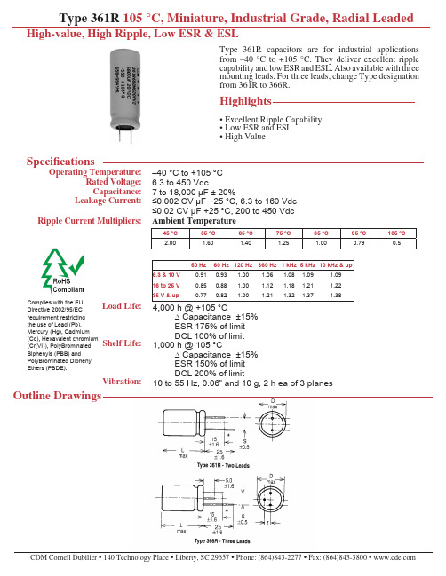
4,000 h @ +105 °C∆ Capacitance ±15% ESR 175% of limit DCL 100% of limit 1,000 h @ 105 °C∆ Capacitance ±15% ESR 150% of limit DCL 200% of limit10 to 55 Hz, 0.06” and 10 g, 2 h ea of 3 planesType 361R capacitors are for industrial applications from –40 °C to +105 °C. They deliver excellent ripple capability and low ESR and ESL. Also available with three mounting leads. For three leads, change Type designation from 361R to 366R.Highlights• Excellent Ripple Capability • Low ESR and ESL • High ValueSpecificationsOperating Temperature:Rated Voltage:Capacitance:Leakage Current:Ripple Current Multipliers:Load Life:Shelf Life:Vibration:–40 °C to +105 °C 6.3 to 450 Vdc7 to 18,000 µF ± 20%≤0.002 CV µF +25 °C, 6.3 to 160 Vdc ≤0.02 CV µF +25 °C, 200 to 450 Vdc Ambient Temperature45 °C 55 °C 65 °C 75 °C 85 °C 95 °C 105 °C 2.001.601.401.251.000.790.550 Hz60 Hz 120 Hz 360 Hz 1 kHz 5 kHz 10 kHz & up 6.3 & 10 V 0.910.93 1.00 1.06 1.08 1.09 1.0916 to 25 V0.850.88 1.00 1.12 1.18 1.21 1.2235 V & up0.770.821.001.211.321.371.38Outline DrawingsComplies with the EU Directive 2002/95/EC requirement restricting the use of Lead (Pb), Mercury (Hg), Cadmium (Cd), Hexavalent chromium (Cr(VI)), PolyBrominated Biphenyls (PBB) andPolyBrominated Diphenyl Ethers (PBDE).Part Numbering System361R TypeEEpoxy End Seal2InsulationLVCase Code6R3VoltageMTolerance183Capacitance(blank) = no epoxyE = Epoxy0 = None2 = PVC6R3 = 6.3 Vdc063 = 63 VdcM = ±20%U = –10 + 75%100 = 10 µF101 = 100 µF183 = 18000 µF361R or 366RNominal Insulated Insulated S T Lead Diam. Weight Case D x L D x L Epoxy Seal ± 0.6± 0.5mm AWG g Code(mm)(mm)(mm)(mm) (mm)EG12.5 x 20.0 13.0 x 21.5 13.0 x 23.0 5.0 2.50.8120 3.8 EK12.5 x 25.0 13.0 x 26.5 13.0 x 29.0 5.0 2.50.8120 4.5 EM12.5 x 26.5 13.0 x 28.0 13.0 x 29.5 5.0 2.50.8120 4.7 EN12.5 x 33.5 13.0 x 34.2 13.0 x 36.0 5.0 2.50.8120 5.8 ER12.5 x 42.5 13.0 x 43.7 13.0 x 45.5 5.0 2.50.81207.3 FK16.0 x 25.0 16.5 x 26.2 16.5 x 27.9 7.5 3.750.81207.2 FF16.0 x 32.0 16.5 x 33.5 16.5 x 36.0 7.5 3.750.81209.4 FN 16.0 x 33.5 16.5 x 34.2 16.5 x 36.0 7.5 3.750.81209.5 FQ 16.0 x 36.0 16.5 x 37.5 16.5 x 40.0 7.5 3.750.812010.6 FV 16.0 x 40.0 16.5 x 41.7 16.5 x 42.4 7.5 3.750.812011.9 LQ 18.0 x 36.0 18.5 x 37.5 18.5 x 40.0 7.5 3.750.812013.4 LV 18.0 x 40.0 18.5 x 42.0 18.5 x 43.0 7.5 3.750.812014.9 HH 22.0 x 22.0 22.5 x 23.5 22.5 x 26.0 10.0 5.00.812011.0 HK 22.0 x 25.0 22.5 x 26.2 22.5 x 27.9 10.0 5.00.812013.5 HG 22.0 x 30.0 22.5 x 32.5 22.5 x 34.0 10.0 5.00.812015.1Typical Performance CurvesL incl. Sleeve & Epoxy Seal - MillimetersESR Max. 120 Hz 25ºC (Ω)Ripple A120 Hz85ºC (A)Nom SizeD X L(mm)ESR Max.120 Hz25ºC (Ω)Ripple A120 Hz85ºC (A)Nom SizeD X L(mm)Cap. (µF)CatalogPart NumberCap.(µF)CatalogPart Number6.3 Vdc (8 Vdc Surge) 20 Vdc (25 Vdc Surge)2200361R222M6R3EG2 0.205 1.13012.5 x 20 1000361R102M020EG2 0.2000.97012.5 x 20 3300361R332M6R3EK2 0.140 1.44012.5 x 25 1500361R152M020EK2 0.133 1.30012.5 x 25 3900361R392M6R3EM2 0.131 1.38012.5 x 26.5 2200361R222M020EM2 0.103 1.51012.5 x 26.5 4700361R472M6R3EN2 0.098 1.84012.5 x 33.5 2700361R272M020EN2 0.084 1.84012.5 x 33.5 6800361R682M6R3ER2 0.075 2.16012.5 x 42.5 3300361R332M020FK2 0.076 2.00016 x 25 6800361R682M6R3FK2 0.084 2.00016 x 25 3300361R332M020HH2 0.076 2.32022 x 22 6800361R682M6R3HH2 0.091 2.20022 x 22 3900361R392M020ER2 0.065 2.32012.5 x 42.5 8200361R822M6R3HK2 0.075 2.33022 x 25 3900361R392M020HK2 0.065 2.50022 x 25 10000361R103M6R3FF2 0.068 2.33016 x 32 4700361R472M020FF2 0.060 2.48016 x 32 10000361R103M6R3HG2 0.046 3.29022 x 30 5600361R562M020FQ2 0.055 2.72016 x 36 12000361R123M6R3FQ2 0.062 2.55016 x 36 6800361R682M020FV2 0.053 2.90016 x 40 12000361R123M6R3FV2 0.058 2.75016 x 40 6800361R682M020HG2 0.047 3.33022 x 30 15000361R153M6R3HV2 0.044 3.42022 x 40 8200361R822M020LQ2 0.047 3.18018 x 36 15000361R153M6R3LQ2 0.053 2.99018 x 36 10000361R103M020HV2 0.044 3.75022 x 40 18000361R183M6R3LV2 0.049 3.24018 x 40 10000361R103M020LV2 0.044 3.28018 x 4010 Vdc (12.5 Vdc Surge)25 Vdc (32 Vdc Surge)1500361R152M010EG2 0.2100.94712.5 x 20 820361R821M025EG2 0.2800.86012.5 x 20 2200361R222M010EK2 0.158 1.33012.5 x 25 1000361R102M025EK2 0.230 1.08012.5 x 25 2700361R272M010EM2 0.144 1.42012.5 x 26.5 1200361R122M025EM2 0.190 1.15012.5 x 26.5 3300361R332M010EN2 0.115 1.76012.5 x 33.5 1800361R182M025EN2 0.128 1.55012.5 x 33.5 4700361R472M010ER2 0.083 2.25012.5 x 42.5 2200361R222M025FK2 0.121 1.66016 x 25 4700361R472M010FK2 0.093 2.00016 x 25 2200361R222M025HH2 0.121 1.84022 x 22 4700361R472M010HH2 0.094 2.17022 x 22 2700361R272M025ER2 0.096 2.00012.5 x 42.5 5600361R562M010HK2 0.074 2.54022 x 25 3300361R332M025FF2 0.091 2.08016 x 32 6800361R682M010FF2 0.073 2.44016 x 32 3300361R332M025HK2 0.091 2.23022 x 25 8200361R822M010FQ2 0.063 2.95016 x 36 3900361R392M025FK2 0.081 2.36016 x 36 8200361R822M010HG2 0.052 3.17022 x 30 4700361R472M025FV2 0.071 2.56016 x 40 10000361R103M010FV2 0.059 3.00016 x 40 4700361R472M025HG2 0.071 2.75022 x 30 12000361R123M010HV2 0.046 3.39022 x 40 4700361R472M025LQ2 0.071 2.71018 x 36 12000361R123M010LQ2 0.056 3.05018 x 36 5600361R562M025LV2 0.065 2.83018 x 40 15000361R153M010LV2 0.051 3.40018 x 40 6800361R682M025HV2 0.053 3.61022 x 4016 Vdc (20 Vdc Surge) 35 Vdc (44 Vdc Surge)1000361R102M016EG2 0.2650.94212.5 x 20 680361R681M035EG2 0.2870.85012.5 x 20 1800361R182M016EK2 0.156 1.35012.5 x 25 1000361R102M035EK2 0.199 1.20012.5 x 25 2200361R222M016EM2 0.147 1.41012.5 x 26.5 1200361R122M035EM2 0.190 1.25012.5 x 26.5 3300361R332M016EN2 0.108 1.79012.5 x 33.5 1500361R152M035EN2 0.133 1.57012.5 x 33.5 3300361R332M016FK2 0.100 1.88016 x 25 1800361R182M035FK2 0.133 1.62016 x 25 3300361R332M016HH2 0.100 2.08022 x 22 1800361R182M035HH2 0.110 1.84022 x 22 4700361R472M016ER2 0.084 2.20012.5 x 42.5 2200361R222M035ER2 0.106 1.90012.5 x 42.5 4700361R472M016FF2 0.077 2.28016 x 32 2200361R222M035FF2 0.106 2.00016 x 32 4700361R472M016HK2 0.082 2.43022 x 25 2700361R272M035FQ2 0.086 2.33016 x 36 6800361R682M016FQ2 0.066 2.67016 x 36 2700361R272M035HK2 0.086 2.18022 x 25 6800361R682M016FV2 0.064 2.70016 x 40 3300361R332M035FV2 0.080 2.38016 x 40 6800361R682M016HG2 0.014 3.11022 x 30 3300361R332M035HG2 0.081 2.57022 x 30 7800361R782M016LQ2 0.060 2.80018 x 36 3300361R332M035LQ2 0.080 2.40018 x 36 9000361R902M016HV2 0.011 3.59022 x 40 4700361R472M035HV2 0.064 3.27022 x 40 10000361R103M016LV2 0.053 3.00018 x 40 4700361R472M035LV2 0.064 2.70018 x 40ESR Max. 120 Hz 25ºC (Ω)Ripple A120 Hz85ºC (A)Nom SizeD X L(mm)ESR Max.120 Hz25ºC (Ω)Ripple A120 Hz85ºC (A)Nom SizeD X L(mm)Cap. (µF)CatalogPart NumberCap.(µF)CatalogPart Number50 Vdc (63 Vdc Surge) 100 Vdc (125 Vdc Surge)330361R331M050EG2 0.4430.76012.5 x 20 100361R101M100EG2 1.6500.35512.5 x 20 470361R471M050EK2 0.3430.96012.5 x 25 120361R121M100EK2 1.3200.45012.5 x 25 560361R561M050EM2 0.266 1.05012.5 x 26.5 150361R151M100EM2 1.1000.50012.5 x 26.5 820361R821M050EN2 0.180 1.38012.5 x 33.5 220361R221M100EN2 0.7500.66612.5 x 33.5 820361R821M050HH2 0.190 1.56022 x 22 220361R221M100HH2 0.7500.76022 x 22 1000361R102M050FK2 0.156 1.53016 x 25 270361R271M100ER2 0.6100.75012.5 x 42.5 1200361R122M050ER2 0.125 1.81012.5 x 42.5 270361R271M100HK2 0.5200.95022 x 25 1500361R152M050FF2 0.101 2.14016 x 32 330361R331M100FK2 0.5000.87516 x 25 1500361R152M050HK2 0.106 2.16022 x 25 390361R391M100FF2 0.420 1.01016 x 32 1800361R182M050FQ2 0.083 2.44016 x 36 470361R471M100FQ2 0.350 1.15016 x 36 1800361R182M050HG2 0.084 2.49022 x 30 470361R471M100FV2 0.350 1.25016 x 40 2200361R222M050LQ2 0.081 2.64018 x 36 470361R471M100HG2 0.351 1.25022 x 30 2200361R222M050FV2 0.081 2.60016 x 40 560361R561M100LQ2 0.290 1.37018 x 36 2700361R272M050HV2 0.067 3.19022 x 40 680361R681M100HV2 0.241 1.69022 x 40 2700361R272M050LV2 0.065 3.04018 x 40 680361R681M100LV2 0.240 1.57018 x 4063 Vdc (79 Vdc Surge) 160 Vdc (185 Vdc Surge)330361R331M063EG2 0.4500.76012.5 x 20 33361R330M160EG2 5.0000.20012.5 x 20 470361R471M063EK2 0.3180.96012.5 x 25 47361R470M160EK2 3.5000.25012.5 x 25 470361R471M063EM2 0.3180.98012.5 x 26.5 56361R560M160EM2 2.9500.28012.5 x 26.5 560361R561M063EN2 0.268 1.15012.5 x 33.5 82361R820M160EN2 2.0000.38012.5 x 33.5 680361R681M063ER2 0.183 1.54012.5 x 42.5 100361R101M160ER2 1.6500.46012.5 x 42.5 820361R821M063FK2 0.220 1.31016 x 25 100361R101M160FK2 1.6500.43016 x 25 820361R821M063HH2 0.220 1.42022 x 22 100361R101M160HH2 1.6500.47522 x 22 1200361R122M063FF2 0.150 1.70016 x 32 150361R151M160FF2 1.1000.58016 x 32 1200361R122M063HK2 0.150 1.81022 x 25 150361R151M160HK2 1.1000.61022 x 25 1500361R152M063FQ2 0.125 1.98016 x 36 180361R181M160FQ2 0.9200.66516 x 36 1500361R152M063HG2 0.099 2.31022 x 30 220361R221M160FV2 0.7500.77016 x 40 1800361R182M063FV2 0.100 2.30016 x 40 220361R221M160HG2 0.7510.84022 x 30 1800361R182M063LQ2 0.100 2.58018 x 36 220361R221M160LQ2 0.7500.80018 x 36 2200361R222M063HV2 0.072 2.99022 x 40 270361R271M160LV2 0.6100.92018 x 40 2200361R222M063LV2 0.083 2.70018 x 40 330361R331M160HV2 0.5120.99022 x 4075 Vdc (90 Vdc Surge) 200 Vdc (225 Vdc Surge)150361R151M075EG2 1.0700.45012.5 x 20 27361R270M200EG2 5.9000.17512.5 x 20 220361R221M075EK2 0.7270.58012.5 x 25 47361R470M200EK2 3.6000.25012.5 x 25 270361R271M075EM2 0.6000.65012.5 x 26.5 56361R560M200EM2 3.0000.28012.5 x 26.5 390361R391M075EN2 0.4100.87012.5 x 33.5 68361R680M200EN2 2.5000.34012.5 x 33.5 470361R471M075FK2 0.340 1.00016 x 25 82361R820M200FK2 2.0000.39016 x 25 470361R471M075HH2 0.340 1.04022 x 22 82361R820M200HH2 2.0000.43022 x 22 560361R561M075ER2 0.285 1.16012.5 x 42.5 100361R101M200ER2 1.6500.45012.5 x 42.5 680361R681M075FF2 0.235 1.32016 x 32 120361R121M200FF2 1.3800.52016 x 32 680361R681M075HK2 0.235 1.31022 x 25 120361R121M200HK2 1.3800.54522 x 25 820361R821M075FQ2 0.195 1.52016 x 36 150361R151M200FQ2 1.1000.60016 x 36 1000361R102M075FV2 0.160 1.66016 x 40 180361R181M200HG2 1.0000.73022 x 30 1000361R102M075HG2 0.161 1.81022 x 30 220361R221M200FV2 0.7600.76016 x 40 1000361R102M075LQ2 0.160 1.70018 x 36 220361R221M200LQ2 0.7600.79018 x 36 1200361R122M075LV2 0.133 1.90018 x 40 270361R271M200HV2 0.7810.94022 x 40 1500361R152M075HV2 0.107 2.53022 x 40 270361R271M200LV2 0.6200.91018 x 40ESR Max. 120 Hz 25ºC (Ω)Ripple A120 Hz85ºC (A)Nom SizeD X L(mm)ESR Max.120 Hz25ºC (Ω)Ripple A120 Hz85ºC (A)Nom SizeD X L(mm)Cap. (µF)CatalogPart NumberCap.(µF)CatalogPart Number250 Vdc (300 Vdc Surge) 33361R330M350HH2 5.0000.27522 x 2218361R180M250EG2 9.2000.14512.5 x 20 39361R390M350FF2 4.2500.29516 x 32 27361R270M250EK2 6.1000.19012.5 x 25 47361R470M350FQ2 3.5000.34016 x 36 33361R330M250EM2 5.0000.21512.5 x 26.5 47361R470M350HK2 3.5000.34022 x 25 47361R470M250EN2 3.5000.28512.5 x 33.5 56361R560M350FV2 2.9500.38516 x 40 47361R470M250FK2 3.5000.29516 x 25 56361R560M350HG2 2.9500.42022 x 30 56361R560M250ER2 2.9500.34512.5 x 42.5 68361R680M350LQ2 2.4200.44518 x 36 56361R560M250HH2 2.9500.35022 x 22 82361R820M350HV2 2.0000.59022 x 40 68361R680M250FF2 2.4200.39016 x 32 82361R820M350LV2 2.0000.50018 x 40 82361R820M250FQ2 2.0000.45016 x 36 400 Vdc (450 Vdc Surge)82361R820M250HK2 2.0000.45022 x 25 8361R080M400EK2 20.000.10512.5 x 25 100361R101M250FV2 1.6500.51516 x 40 12361R120M400EM2 13.800.12512.5 x 26.5 120361R121M250HG2 1.3800.62022 x 30 18361R180M400EN2 9.1000.17512.5 x 33.5 120361R121M250LQ2 1.3800.58518 x 36 22361R220M400FK2 7.5000.20016 x 25 150361R151M250LV2 1.1000.68518 x 40 27361R270M400ER2 6.1000.23512.5 x 42.5 180361R181M250HV2 0.9210.88022 x 40 33361R330M400FF2 5.0000.27516 x 32 300 Vdc (365 Vdc Surge)33361R330M400HH2 5.0000.27522 x 22 12361R120M300EG2 13.800.12012.5 x 20 39361R390M400FQ2 4.2000.31516 x 36 18361R180M300EK2 9.1500.15512.5 x 25 39361R390M400HK2 4.2000.31522 x 25 22361R220M300EM2 7.5000.17512.5 x 26.5 47361R470M400FV2 3.5000.35516 x 40 33361R330M300EN2 5.0000.24012.5 x 33.5 47361R470M400HG2 3.5100.39022 x 30 33361R330M300FK2 5.0000.24516 x 25 56361R560M400LQ2 2.9500.40018 x 36 39361R390M300HH2 4.2500.29522 x 22 68361R680M400HV2 2.4200.53022 x 40 47361R470M300ER2 3.5000.31512.5 x 42.5 68361R680M400LV2 2.4200.46518 x 40 47361R470M300FF2 3.5000.32516 x 32 450 Vdc (500 Vdc Surge)56361R560M300FQ2 2.9500.37516 x 36 7361R070M450EK2 20.000.10012.5 x 25 56361R560M300HK2 2.9500.37522 x 25 10361R100M450EM2 16.500.12012.5 x 26.5 68361R680M300FV2 2.4200.43016 x 40 15361R150M450EN2 11.000.16512.5 x 33.5 68361R680M300HG2 2.4200.48022 x 30 18361R180M450FK2 9.1000.18516 x 25 82361R820M300LQ2 2.0000.48518 x 36 22361R220M450ER2 7.5000.21512.5 x 42.5 100361R101M300HV2 1.6500.65022 x 40 27361R270M450FF2 6.1000.24516 x 32 100361R101M300LV2 1.6500.55518 x 40 27361R270M450HH2 6.1000.24522 x 22 350 Vdc (400 Vdc Surge) 33361R330M450FQ2 5.0000.28516 x 36 10361R100M350EK2 16.500.11512.5 x 25 33361R330M450HK2 5.0000.30022 x 25 15361R150M350EM2 11.000.14512.5 x 26.5 39361R390M450FV2 4.2000.32516 x 40 22361R220M350EN2 7.5000.19512.5 x 33.5 39361R390M450HG2 4.2000.35022 x 30 27361R270M350FK2 6.1000.22516 x 25 47361R470M450LQ2 3.5000.36518 x 36 33361R330M350ER2 5.0000.26512.5 x 42.5 56361R560M450LV2 2.9500.41518 x 4068361R680M450HV2 2.4500.53022 x 40。
730-BT 安全技术说明书
安全技术说明书according to SAC GB 30000-2013____________________________________________________________________________________________________________________。
SDS # : 730-BT730-BT。
第 1 部分部分:: 化学品及企业标识。
产品名称730-BT确定用途胶粘剂。
有关更多信息,请联系: 接触点洪志明电子邮件地址。
紧急电话Chemtrec @ 001-703-741-5970 (24hrs)香港0800-968-793中国4001-204937。
第 2 部分部分:: 危害标识。
G H S - 分类 皮肤腐蚀/刺激类别2严重眼损伤/眼刺激类别2A 皮肤致敏类别1B 急性水生毒性类别2慢性水生毒性类别2。
标签元素修订日期 2015-09-10版本 1。
制造商Dymax Corporation 318 Industrial Lane Torrington, CT 06790Tel: 860-482-1010Fax: 860-496-0608签发日期 2015-09-10供应商戴马斯紫外线胶水设备(上海)有限公司上海市金山区秋实路688号A 5 407/409/411____________________________________________________________________________________________________________________。
信号词警告危险性说明H315-造成皮肤刺激H317-可能导致皮肤过敏反应H319-造成严重眼刺激H411-对水生生物有毒并具有长期持续影响。
防范说明 -预防P264-作业后彻底清洗脸部、手部和任何暴露的皮肤戴防护手套/穿防护服/戴防护眼罩/戴防护面具避免吸入粉尘/烟气/气体/烟雾/蒸汽/喷雾受沾染的工作服不得带出工作场地避免释放到环境中防范说明 -响应如接触到或有疑虑:求医/就诊如进入眼睛:用水小心清洗几分钟。
杭州士兰微电子股份有限公司 SC7A20 三轴微机械数字加速度传感器说明书

±2G/±4G/±8G/±16G三轴微机械数字加速度计描述SC7A20是一款高精度12bit数字三轴加速度传感器芯片,内置功能更丰富,功耗更低,体积更小,测量更精确。
芯片通过I²C/SPI接口与MCU通信,加速度测量数据以中断方式或查询方式获取。
INT1和INT2中断管脚提供多种内部自动检测的中断信号,适应多种运动检测场合,中断源包括6D/4D方向检测中断信号、自由落体检测中断信号、睡眠和唤醒检测中断信号、单击和双击检测中断信号。
芯片内置高精度校准模块,对传感器的失调误差和增益误差进行精确补偿。
±2G、±4G、±8G和±16G四种可调整的全量程测量范围,灵活测量外部加速度,输出数据率1HZ和400HZ间可选。
芯片内置自测试功能允许客户系统测试时检测系统功能,省去复杂的转台测试。
芯片内置产品倾斜校准功能,对贴片和板卡安装导致的倾斜进行补偿,不占系统资源,系统文件升级不影响传感器参数。
主要特点宽电压范围1.71V-3.6V1.8V兼容数字IO口低功耗模式下电源电流低至2µA±2G/±4G/±8G/±16G动态全量程范围 12bit有效数据(HR)I²C/SPI数字输出接口6D/4D方向检测自由落体检测单击双击检测及运动检测可编程中断生成电路内嵌自测试功能内嵌FIFO10000g高G抗击能力应用手机平板室内导航图像旋转运动激活用户接口游戏产品规格分类产品名称 封装形式 打印名称 材料 包装形式 SC7A20TR LGA-12-2x2x1.0 SC7A20 无铅编带内部框图XY ZC-to-V Converter Gain数符号测试条件最小值V CC电路不损坏-0.3 3.6V P电路不损坏V in电路不损坏T OPR电路不损坏T STG电路不损坏(VDD=2.5V, T测试条件123FS=0 (HR mode)FS=1 (HR mode)FS=2 (HR mode)FS=3 (HR mode)参 数符 号测试条件最小值 典型值 最大值 单位 零漂 Ty Off0 FS =0 --±40--mg温漂TC Off 与25°C 的最大偏差 -- ±0.5 -- mg/°C 自测输出V st1FS=0, X 轴 -- 276 -- LSb V st2 FS=0, Y 轴 -- 276 -- LSb V st3FS=0, Z 轴-- 984 -- LSb 系统带宽 BW -- ODR/2 -- HZ 工作温度T OPR-40--+85°C注意:电路2.5V 出厂校准。
P4SMA13A-E361,P4SMA160A-E61,P4SMA27CA-E35A,P4SMA13AHE361,P4SMA27CA-E361, 规格书,Datasheet 资料
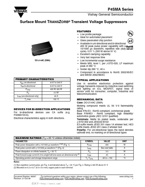
P4SMA SeriesVishay General SemiconductorDocument Number: 88367For technical questions within your region, please contact one of the following:Surface Mount T RANS Z ORB ® Transient Voltage SuppressorsFEATURES•Low profile package•Ideal for automated placement •Glass passivated chip junction•10/1000 µs cycle): 0.01 % (300 W above 91 V) •Excellent clamping capability •Very fast response time•Low incremental surge resistance•Meets MSL level 1, per J-STD-020, LF maximum peak of 260 °C•Solder dip 260 °C, 40 s •Component in accordance to RoHS 2002/95/EC and WEEE 2002/96/EC TYPICAL APPLICATIONSUse in sensitive electronics protection against voltage transients induced by inductive load switching and lighting on I Cs, MOSFET, signal lines of sensor units for consumer, computer, industrial and telecommunication.MECHANICAL DATA Case: DO-214AC (SMA)Molding compound meets UL 94 V-0 flammability ratingBase P/N-E3 - RoHS compliant, commercial grade Base P/NHE3 - RoHS compliant, high reliability/automotive grade (AEC Q101 qualified)Terminals: Matte tin plated leads, solderable per J-STD-002 and JESD22-B102E3 suffix meets JESD 201 class 1A whisker test, HE3suffix meets JESD 201 class 2 whisker testPolarity: For uni-directional types the band denotes cathode end, no marking on bi-directional typesDEVICES FOR BI-DIRECTION APPLICATIONS For bi-directional devices use CA suffix (e.g.P4SMA10CA).Electrical characteristics apply in both directions.PRIMARY CHARACTERISTICSV BR uni-directional 6.8 V to 540 V V BR bi-directional6.8 V to 220 V P PPM 400 W, 300 WP D3.3 W I FSM (uni-directional only)40 A T J max.150 °CDO-214AC (SMA)Notes:(1) Non-repetitive current pulse, per Fig. 3 and derated above T A = 25 °C per Fig. 2. Rating is 300 W above 91 V (2) Mounted on 0.2 x 0.2" (5.0 x 5.0 mm) copper pads to each terminalMAXIMUM RATINGS (T A = 25°C unless otherwise noted)PARAMETERSYMBOL VALUE UNITPeak power dissipation with a 10/1000 µs waveform (1)(2) (Fig. 1) P PPM 400W Peak pulse current with a 10/1000 µs waveform (1) (Fig. 3) I PPM See next tableA Power dissipation on infinite heatsink, T A = 50 °CP D 3.3W Peak forward surge current 8.3 ms single half sine-wave uni-directional only (2) I FSM 40 A Operating junction and storage temperature range T J , T STG- 65 to + 150°CP4SMA SeriesVishay General Semiconductor For technical questions within your region, please contact one of the following:Document Number: 88367Notes:(1) Pulse test: t p ≤ 50 ms(2) Surge current waveform per Fig. 3 and derate per Fig. 2(3) All terms and symbols are consistent with ANSI/IEEE CA62.35(4) For bi-directional types with V R 10 V and less, the I D limit is doubled (5) V F = 3.5 V at I F = 25 A (uni-directional only)ELECTRICAL CHARACTERISTICS (T A = 25°C unless otherwise noted)PART NUMBERDEVICE MARKING CODE BREAKDOWN VOLTAGE V BR AT I T (1) TESTCURRENTI T (mA)STAND-OFF VOLTAGE V WM (V)MAXIMUMREVERSELEAKAGEAT V WM I D (4) (µA)MAXIMUM PEAK PULSE CURRENT I PPM (2) (A) MAXIMUMCLAMPINGVOLTAGEAT I PPMV C (V)MAXIMUMTEMPERATUREOF V BR(%/°C)UNIBIMIN.MAX.P4SMA6.8A 6V8A 6V8C 6.457.1410 5.80100038.110.50.057P4SMA7.5A 7V5A 7V5C 7.137.8810 6.4050035.411.30.061P4SMA8.2A 8V2A 8V2C 7.798.61107.0220033.112.10.065P4SMA9.1A 9V1A 9V1C 8.659.55 1.07.7850.029.913.40.068P4SMA10A 10A 10C 9.510.5 1.08.5510.027.614.50.073P4SMA11A 11A 11C 10.511.6 1.09.40 5.025.615.60.075P4SMA12A 12A 12C 11.412.6 1.010.2 1.024.016.70.078P4SMA13A 13A 13C 12.413.7 1.011.1 1.022.018.20.081P4SMA15A 15A 15C 14.315.8 1.012.8 1.018.921.20.084P4SMA16A 16A 16C 15.216.8 1.013.6 1.017.822.50.086P4SMA18A 18A 18C 17.118.9 1.015.3 1.015.925.20.089P4SMA20A 20A 20C 19.021.0 1.017.1 1.014.427.70.090P4SMA22A 22A 22C 20.923.1 1.018.8 1.013.130.60.092P4SMA24A 24A 24C 22.825.2 1.020.5 1.012.033.20.090P4SMA27A 27A 27C 25.728.4 1.023.1 1.010.737.50.096P4SMA30A 30A 30C 28.531.5 1.025.6 1.09.741.40.097P4SMA33A 33A 33C 31.434.7 1.028.2 1.08.845.70.098P4SMA36A 36A 36C 34.237.8 1.030.8 1.08.049.90.099P4SMA39A 39A 39C 37.141.0 1.033.3 1.07.453.90.100P4SMA43A 43A 43C 40.945.2 1.036.8 1.0 6.759.30.101P4SMA47A 47A 47C 44.749.4 1.040.2 1.0 6.264.80.101P4SMA51A 51A 51C 48.553.6 1.043.6 1.0 5.770.10.102P4SMA56A 56A 56C 53.258.8 1.047.8 1.0 5.277.00.103P4SMA62A 62A 62C 58.965.1 1.053.0 1.0 4.785.00.104P4SMA68A 68A 68C 64.671.4 1.058.1 1.0 4.392.00.104P4SMA75A 75A 75C 71.378.8 1.064.1 1.0 3.91040.105P4SMA82A 82A 82C 77.986.1 1.070.1 1.0 3.51130.105P4SMA91A 91A 91C 86.595.5 1.077.8 1.0 3.21250.106P4SMA100A 100A 100C 95.0105 1.085.5 1.0 2.21370.106P4SMA110A 110A 110C 105116 1.094.0 1.0 2.01520.107P4SMA120A 120A 120C 114126 1.0102 1.0 1.81650.107P4SMA130A 130A 130C 124137 1.0111 1.0 1.71790.107P4SMA150A 150A 150C 143158 1.0128 1.0 1.42070.106P4SMA160A 160A 160C 152168 1.0136 1.0 1.42190.108P4SMA170A 170A 170C 162179 1.0145 1.0 1.32340.108P4SMA180A 180A 180C 171189 1.0154 1.0 1.22460.108P4SMA200A 200A 200C 190210 1.0171 1.0 1.12740.108P4SMA220A 220A 220C 209231 1.0185 1.00.903280.108P4SMA250A 250A -237263 1.0214 1.00.873440.110P4SMA300A 300A - 285315 1.0256 1.00.734140.110P4SMA350A 350A -333368 1.0300 1.00.624820.110P4SMA400A 400A -380420 1.0342 1.00.555480.110P4SMA440A 440A -418462 1.0376 1.00.506020.110P4SMA480A 480A -456504 1.0408 1.00.466580.110P4SMA510A 510A -485535 1.0434 1.00.436980.110P4SMA540A 540A -5135671.04591.00.417400.110P4SMA SeriesVishay General SemiconductorDocument Number: 88367For technical questions within your region, please contact one of the following:Note:(1) Mounted on minimum recommended pad layoutNote:(1) Automotive grade AEC Q101 qualifiedRATINGS AND CHARACTERISTICS CURVES (T A = 25 °C unless otherwise noted)THERMAL CHARACTERISTICS (T A = 25°C unless otherwise noted)PARAMETERSYMBOLVALUEUNITThermal resistance, junction to ambient air (1) R θJA 120°C/W Thermal resistance, junction to leadsR θJL 30°C/WORDERING INFORMATION (Example)PREFERRED P/N UNIT WEIGHT (g)PREFERRED PACKAGE CODEBASE QUANTITYDELIVERY MODEP4SMA6.8A-E3/610.0646118007" diameter plastic tape and reel P4SMA6.8A-E3/5A 0.0645A 750013" diameter plastic tape and reel P4SMA6.8AHE3/61 (1)0.0646118007" diameter plastic tape and reel P4SMA6.8AHE3/5A (1)0.0645A750013" diameter plastic tape and reelFigure 1. Peak Pulse Power Rating Curve Figure 2. Pulse Power or Current vs. Initial Junction TemperatureFigure 3. Pulse WaveformFigure 4. Typical Junction CapacitanceP4SMA SeriesVishay General Semiconductor For technical questions within your region, please contact one of the following:Document Number: 88367PACKAGE OUTLINE DIMENSIONS in inches (millimeters)Figure 5. Typical Transient Thermal ImpedanceFigure 6. Maximum Non-Repetitive Forward Surge CurrentUni-Directional OnlyLegal Disclaimer Notice VishayDisclaimerALL PRODU CT, PRODU CT SPECIFICATIONS AND DATA ARE SU BJECT TO CHANGE WITHOU T NOTICE TO IMPROVE RELIABILITY, FUNCTION OR DESIGN OR OTHERWISE.Vishay Intertechnology, Inc., its affiliates, agents, and employees, and all persons acting on its or their behalf (collectively,“Vishay”), disclaim any and all liability for any errors, inaccuracies or incompleteness contained in any datasheet or in any other disclosure relating to any product.Vishay makes no warranty, representation or guarantee regarding the suitability of the products for any particular purpose or the continuing production of any product. To the maximum extent permitted by applicable law, Vishay disclaims (i) any and all liability arising out of the application or use of any product, (ii) any and all liability, including without limitation special, consequential or incidental damages, and (iii) any and all implied warranties, including warranties of fitness for particular purpose, non-infringement and merchantability.Statements regarding the suitability of products for certain types of applications are based on Vishay’s knowledge of typical requirements that are often placed on Vishay products in generic applications. Such statements are not binding statements about the suitability of products for a particular application. It is the customer’s responsibility to validate that a particular product with the properties described in the product specification is suitable for use in a particular application. Parameters provided in datasheets and/or specifications may vary in different applications and performance may vary over time. All operating parameters, including typical parameters, must be validated for each customer application by the customer’s technical experts. Product specifications do not expand or otherwise modify Vishay’s terms and conditions of purchase, including but not limited to the warranty expressed therein.Except as expressly indicated in writing, Vishay products are not designed for use in medical, life-saving, or life-sustaining applications or for any other application in which the failure of the Vishay product could result in personal injury or death. Customers using or selling Vishay products not expressly indicated for use in such applications do so at their own risk and agree to fully indemnify and hold Vishay and its distributors harmless from and against any and all claims, liabilities, expenses and damages arising or resulting in connection with such use or sale, including attorneys fees, even if such claim alleges that Vishay or its distributor was negligent regarding the design or manufacture of the part. Please contact authorized Vishay personnel to obtain written terms and conditions regarding products designed for such applications.No license, express or implied, by estoppel or otherwise, to any intellectual property rights is granted by this document or by any conduct of Vishay. Product names and markings noted herein may be trademarks of their respective owners.Material Category PolicyVishay Intertechnology, Inc. hereb y certifies that all its products that are identified as RoHS-Compliant fulfill the definitions and restrictions defined under Directive 2011/65/EU of The European Parliament and of the Council of June 8, 2011 on the restriction of the use of certain hazardous substances in electrical and electronic equipment (EEE) - recast, unless otherwise specified as non-compliant.Please note that some Vishay documentation may still make reference to RoHS Directive 2002/95/EC. We confirm that all the products identified as being compliant to Directive 2002/95/EC conform to Directive 2011/65/EU.Revision: 12-Mar-121Document Number: 91000。
AS7C31026A-12中文资料
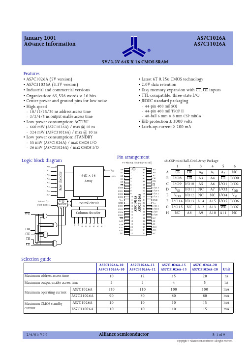
January 2001Advance Information®AS7C1026A AS7C31026A5V/3.3V 64K X 16 CMOS SRAMFeatures•AS7C1026A (5V version)•AS7C31026A (3.3V version)•Industrial and commercial versions •Organization: 65,536 words × 16 bits•Center power and ground pins for low noise •High speed-10/12/15/20 ns address access time -3/3/4/5 ns output enable access time•Low power consumption: ACTIVE-660 mW (AS7C1026A) / max @ 10 ns -324 mW (AS7C31026A) / max @ 10 ns•Low power consumption: STANDBY-55 mW (AS7C1026A) / max CMOS I/O -36 mW (AS7C31026A) / max CMOS I/O•Latest 6T 0.25u CMOS technology •2.0V data retention•Easy memory expansion with CE, OE inputs •TTL-compatible, three-state I/O •JEDEC standard packaging-44-pin 400 mil SOJ -44-pin 400 mil TSOP II-48-ball 6 mm × 8 mm CSP mBGA•ESD protection ≥ 2000 volts •Latch-up current ≥ 200 mALogic block diagramCCPin arrangement567891011121314151617181920I/O13I/O12GND V CC I/O11I/O10I/O9I/O8NC A8A9A10A11NCA0CE I/O0I/O1I/O2I/O3V CC GND I/O4I/O5I/O6I/O7WE A15A14A1344-Pin SOJ, TSOP II (400 mil)2122A12NCUB LB I/O15I/O142A33A24A11A440393837363534333231302928272625242343424144A6A7OE A5A S 7C 1026A A S 7C 31026ASelection guideAS7C1026A-10 AS7C31026A-10AS7C1026A-12AS7C31026A-12AS7C1026A-15AS7C31026A-15AS7C1026A-20AS7C31026A-20UnitMaximum address access time 10121520ns Maximum output enable access time 3345ns Maximum operating current AS7C1026A 120110100100mA AS7C31026A 90808080mA Maximum CMOS standby currentAS7C1026A 10101015mA AS7C31026A10101015mA48-CSP mini Ball-Grid-Array Package123456A LB OE A 0A 1A 2NC B I/O8UB A3A4CE I/O0C I/O9I/O10A5A6I/O1I/O2D V SS I/O11NC A7I/O3V DD E V DD I/O12NC NC I/O4V SS F I/O14I/O13A14A15I/O5I/O6G I/O15NC A12A13WE I/O7HNC A8A9A10A11NC®AS7C1026A AS7C31026AFunctional descriptionThe AS7C1026A and AS7C31026A are high-performance CMOS 1,048,576-bit Static Random Access Memory (SRAM) devices organized as 65,536 words × 16 bits. They are designed for memory applications where fast data access, low power, and simple interfacing are desired.Equal address access and cycle times (t AA , t RC , t WC ) of 10/12/15/20 ns with output enable access times (t OE ) of 3/3/4/5 ns are ideal for high-performance applications.When CE is high the devices enter standby mode. The AS7C1026A is guaranteed not to exceed 55 mW power consumption in CMOS standby mode. The devices also offer 2.0V data retention.A write cycle is accomplished by asserting write enable (WE) and chip enable (CE). Data on the input pins I/O0–I/O15 is written on the rising edge of WE (write cycle 1) or CE (write cycle 2). To avoid bus contention, external devices should drive I/O pins only after outputs have been disabled with output enable (OE) or write enable (WE).A read cycle is accomplished by asserting output enable (OE) and chip enable (CE), with write enable (WE) high. the chips drive I/O pins with the data word referenced by the input address. When either chip enable or output enable is inactive, or write enable is active, output drivers stay in high-impedance mode.The devices provide multiple center power and ground pins, and separate byte enable controls, allowing individual bytes to be written and read. LB controls the lower bits, I/O0–I/O7, and UB controls the higher bits, I/O8–I/O15.All chip inputs and outputs are TTL-compatible, and operation is from a single 5V supply (AS7C1026A) or 3.3V supply (AS7C31026A). the device is packaged in common industry standard packages. Chip scale BGA packaging, easy to use in manufacturing, provides the smallest possible footprint. This 48-ball JEDEC-registered package has a ball pitch of 0.75 mm and external dimensions of 8 mm × 6 mm.Absolute maximum ratingsNote: Stresses greater than those listed under Absolute Maximum Ratings may cause permanent damage to the device. This is a stress rating only and functional operation of the device at these or any other conditions outside those indicated in the operational sections of this specification is not implied. Exposure to absolute maximum rating conditions for extended periods may affect reliability .Truth tableKey: H = High, L = Low, X = don’t care.ParameterSymbol Min Max Unit Voltage on V CC relative to GND AS7C1026A V t1–0.50+7.0V AS7C31026AV t1–0.50+5.0V Voltage on any pin relative to GND Both V t2–0.50V CC +0.50V Power dissipationBoth P D – 1.0W Storage temperature (plastic)Both T stg –65+150°C Ambient temperature with VCC appliedBoth T bias –55+125°C DC current into outputs (low)BothI OUT–20mACE WE OE LB UB I/O0–I/O7I/O8–I/O15Mode H X X X X High Z High Z Standby (I SB ), I SBI )L H L L H D OUT High Z Read I/O0–I/O7 (I CC )L H L H L HighZ D OUT Read I/O8–I/O15 (I CC)L H L L L D OUT D OUT Read I/O0–I/O15 (I CC )L L X L L D IN D IN Write I/O0–I/O15 (I CC )L L X L H D IN High Z Write I/O0–I/O7 (I CC )L L X H L HighZ D IN Write I/O8–I/O15 (I CC )L LH XH XX HX HHigh ZHigh ZOutput disable (I CC )®AS7C1026A AS7C31026ARecommended operating conditions† VIL min. = –3.0V for pulse width less than t RC /2.DC operating characteristics (over the operating range)1Capacitance (f = 1MHz, T a = 25 °C, V CC = NOMINAL)2ParameterDevice Symbol Min Nominal Max Unit Supply voltage AS7C1026A V CC 4.5 5.0 5.5V AS7C31026A V CC 3.0 3.3 3.6V Input voltageAS7C1026A V IH 2.2–V CC + 0.5V AS7C31026AV IH 2.0–V CC + 0.5V Both V IL †–0.5–0.8V Ambient operating temperaturecommercial T A 0–70o C industrialT A–40–85o CParameterSymTest conditionsDevice-10-12-15-20UnitMin Max Min Max Min MaxMin Max Input leakage current | I LI |V CC = Max V IN = GND to V CC Both –1–1–1–1µA Output leakage current | I LO |V CC = Max CE = V IH ,V OUT = GND to V CC Both –1–1–1–1µA Operating power supply currentI CCV CC = Max, CE ≤ V ILoutputs open, f = f Max = 1/t RC AS7C1026A –120–110–100–100mA AS7C31026A –90–80–80–80mAStandbypower supply currentI SBV CC = Max, CE ≤ V IL , outputs open,f = f Max = 1/t RC AS7C1026A –30–25–20–20mA AS7C31026A –30–25–20–20I SB1V CC = Max, CE ≥ V CC –0.2V ,V IN ≤ GND + 0.2V or V IN ≥ V CC –0.2V , f = 0AS7C1026A –10–10–10–15mA AS7C31026A –10–10–10–15Output voltage V OL I OL = 8 mA, V CC = Min AS7C1026A –0.4–0.4–0.4–0.4V V OHI OH = –4 mA, V CC = MinAS7C31026A 2.4–2.4–2.4–2.4–V Data retention currentI CCDRV CC = 2.0V CE ≥ V CC –0.2V V IN ≥ V CC –0.2V orV IN ≤ 0.2VAS7C1026A 1115mA AS7C31026A1115mAParameterSymbol SignalsTest conditions Max Unit Input capacitance C IN A, CE, WE, OE, LB, UBV IN = 0V 5pF I/O capacitanceC I/OI/OV IN = V OUT = 0V7pF®AS7C1026A AS7C31026ARead cycle (over the operating range)3,9Key to switching waveforms3,6,7,9Read waveform 2 (OE, CE, UB, LB controlled)3,6,8,9ParameterSymbol -10-12-15-20Unit NotesMin Max MinMax MinMax MinMax Read cycle time t RC 10–12–15–20–ns Address access time t AA –10–12–15–20ns 3Chip enable (CE) access time t ACE –10–12–15–20ns 3Output enable (OE) access time t OE –3–3–4–5ns Output hold from address change t OH 2–3–3–3–ns 5CE Low to output in low Z t CLZ 0–0–0–0–ns 4, 5CE High to output in high Z t CHZ –3–3–4–5ns 4, 5OE Low to output in low Z t OLZ 0–0–0–0–ns 4, 5Byte select access time t BA –3–3–4–5ns Byte select Low to low Z t BLZ 0–0–0–0–ns 4, 5Byte select High to high Z t BHZ –5–6–6–8ns 4, 5OE High to output in high Z t OHZ –3–3–4–5ns 4, 5Power up time t PU 0–0–0–0–ns 4, 5Power down timet PD–10–12–15–20ns4, 5Undefined output/don’t careFalling inputRising inputData Address AddressOECELB, UBData IN®AS7C1026A AS7C31026AWrite cycle (over the operating range) 11ParameterSymbol -10-12-15-20Unit NotesMin Max Min Max Min Max Min MaxWrite cycle timet WC 10–12–15–20–ns Chip enable (CE ) to write end t CW 8–10–12–12–ns Address setup to write end t AW 8–9–10–12–ns Address setup time t AS 0–0–0–0–ns Write pulse widtht WP 7–8–9–12–ns Address hold from end of write t AH 0–0–0–0–ns Data valid to write end t DW 5–6–8–10–ns Data hold timet DH 0–0–0–0–ns 5Write enable to output in high Z t WZ –6–6–6–8ns 4, 5Output active from write end t OW 1–1–1–2–ns 4, 5Byte select low to end of writet BW8–10–12–12–nsAS7C1026A AS7C31026A®Data retention characteristics (over the operating range)Data retention waveformAC test conditionsNotes1DuringV CC power-up, a pull-up resistor to V CC on CE is required to meet I SB specification.2This parameter is sampled, but not 100% tested.3For test conditions, see AC T est Conditions , Figures A, B, and C.4These parameters are specified with C L = 5pF, as in Figures B or C. Transition is measured ± 500 mV from steady-state voltage.5This parameter is guaranteed, but not tested.6WE is High for read cycle.7CE and OE are Low for read cycle.8Address valid prior to or coincident with CE transition Low.9All read cycle timings are referenced from the last valid address to the first transitioning address.10CE or WE must be High during address transitions. Either CE or WE asserting high terminates a write cycle.11All write cycle timings are referenced from the last valid address to the first transitioning address.12Not applicable.13C=30pF, except all high Z and low Z parameters where C=5pF.Parameter Symbol Test conditions Min Max Unit V CC for data retention V DR V CC = 2.0V CE ≥ V CC –0.2V V IN ≥ V CC –0.2V orV IN≤ 0.2V2.0–V Data retention currentI CCDR –1 ma Chip deselect to data retention time t CDR 0–ns Operation recovery time t R t RC –ns Input leakage current|I LI |–1µAV CCCEFigure C: 3.3V Output loadThevenin Equivalent:D OUT +1.728V (5V and 3.3V)Figure B: 5V Output load GND+3.0V Figure A: Input pulseD OUTD OUT–Output load: see Figure B or Figure C.–Input pulse level: GND to 3.0V . See Figure A.–Input rise and fall times: 2 ns. See Figure A.–Input and output timing reference levels: 1.5V .®AS7C1026A AS7C31026APackage dimensions44-pin TSOP II Min (mm)Max (mm)A 1.2A10.05A20.951.05b 0.300.45c 0.127 (typical)D18.2818.54E 10.0310.29He 11.5611.96e 0.80 (typical)l0.400.600–5Seating Plane44-pin SOJ44-pin SOJ 400 milMin (in)Max (in)A 0.1280.148A 10.025–A 20.105 1.115B 0.0260.032b 0.0150.020c 0.0070.013D 1.120 1.130E 0.370 NOM E 10.3950.405E 20.4350.445e0.050 NOMePin 1A 1bBAA 2E 2E 1E 2DcAS7C1026A AS7C31026A®Notes1Bump counts: 48 (8 row x 6 column).2Pitch: (x,y) = 0.75 mm x 0.75 mm (typ).3Units: millimeters.4All tolerance are +/- 0.050 unless otherwisespecified.5Typ: typical.6Y is coplanarity: 0.08 (max).MinimumT ypical MaximumA –0.75–B 5.908.008.10B1– 3.75–C 7.908.008.10C1– 5.25–D –0.35–E –– 1.20E1–0.68–E20.220.250.27Y––0.0848-ball FBGABottom View654321Ball A1C1A B C D F G H JA B1Side ViewTop View Ball #A1 indexCSRAM DIEElastomerBDetail ViewAYDie0.3/T µp E2EDieDE1E2E*pin 1 indicator will show asengraved circle and/or Inc. trade mark*®AS7C1026A AS7C31026A© Copyright Alliance Semiconductor Corporation. All rights reserved. Our three-point logo, our name and Intelliwatt are trademarks or registered trademarks of Alliance. All other brand and product names may be the trademarks of their respective companies. Alliance reserves the right to make changes to this document and its products at any time without notice. Alliance assumes no responsibility for any errors that may appear in this document. The data contained herein represents Alliance’s best data and/or estimates at the time of issuance. Alliance reserves the right to change or correct this data at any time, without notice. If the product described herein is under development, significant changes to these specifications are possible. The information in this product data sheet is intended to be general descriptive information for potential customers and users, and is not intended to operate as, or provide, any guarantee or warrantee to any user or customer. Alliance does not assume any responsibility or liability arising out of the application or use of any product described herein, and disclaims any express or implied warranties related to the sale and/or use of Alliance products including liability or warranties related to fitness for a particular purpose, merchantability, or infringement of any intellectual property rights, except as express agreed to in Alliance’s Terms and Conditions of Sale (which are available from Alliance). All sales of Alliance products are made exclusively according to Alliance’s Terms andConditions of Sale. The purchase of products from Alliance does not convey a license under any patent rights, copyrights, mask works rights, trademarks, or any other intellectual property rights of Alliance or third parties. Alliance does not authorize its products for use as critical components in life-supporting systems where a malfunction or failure may reasonably be expected to result 2/6/01; V .0.9Alliance SemiconductorP. 9 of 9Ordering codesPart numbering systemPackage \ Access time V olt/Temp 10 ns12 ns15 ns20 nsPlastic SOJ, 400 mil5V commercial AS7C1026A-10JC AS7C1026A-12JC AS7C1026A-15JC AS7C1026A-20JC 5V industrial AS7C1026A-10JI AS7C1026A-12JI AS7C1026A-15JI AS7C1026A-20JI 3.3V commercial AS7C31026A-10JCAS7C31026A-12JC AS7C31026A-15JC AS7C31026A-20JC TSOP II, 18.4×10.2 mm5V commercial AS7C1026A-10TC AS7C1026A-12TC AS7C1026A-15TC AS7C1026A-20TC 3.3V commercial AS7C31026A-10TCAS7C31026A-12TC AS7C31026A-15TC AS7C31026A-20TC 3.3V industrial AS7C31026A-10TI AS7C31026A-12TI AS7C31026A-15TI AS7C31026A-20TI CSP BGA, 8×6 mm5V commercialAS7C1026A-10BC AS7C1026A-12BC AS7C1026A-15BC AS7C1026A-20BC 3.3V commercial AS7C31026A-10BCAS7C31026A-12BC AS7C31026A-15BC AS7C31026A-20BC 3.3V industrialAS7C31026A-10BIAS7C31026A-12BIAS7C31026A-15BIAS7C31026A-20BIAS7C X1026–XXXCSRAM prefixBlank=5V CMOS 3=3.3V CMOSDevice number Access timePackage: J=SOJ 400 mil T=TSOP type 2, 18.4 × 10.2 mmB=CSP BGA, 8 × 6 mmT emperature range,C= Commercial: 0° C to 70° C I= Industrial: -40° C to 85° C。
PT7C4363中文资料

Source: Crystal: 32.768kHz
1
Oscillator Oscillator enable/disable
Oscillator fail detect
2
Time
Time display Century bit
12-hour 24-hour
Time count chain enable/disable
元器件交易网
Data Sheet
PT7C4363 Real-time Clock Module (I2C Bus)
|||||||||||||||||||||||||||||||||||||||||||||||||||||||||||||||||||||||||||||||||||||||||||||||||||||||||||||||||||||||||||||||||||||||||||||||||||||||||||||||||||||||||||||||||||||||||||||||||||||||||||||||||||||||||||||||||||||||||||||||||||||||||||||||||||||||||||||||||||||||||||||||||||||||||||||||||||||||||||||||||||||||
8
VCC
P Power.
PT0207(07/05) 3
Ver: 0
元器件交易网 Data Sheet PT7C4363
Real-time Clock Module (I2C Bus)
|||||||||||||||||||||||||||||||||||||||||||||||||||||||||||||||||||||||||||||||||||||||||||||||||||||||||||||||||||||||||||||||||||||||||||||||||||||||||||||||||||||||||||||||||||||||||||||||||||||||||||||||||||||||||||||||||||||||||||||||||||||||||||||||||||||||||||||||||||||||||||||||||||||||||||||||||||||||||||||||||||||||
BY721资料

Fig.4
Maximum permissible average forward current as a function of ambient temperature.
Fig.5
Maximum permissible average forward current as a function of ambient temperature.
Very fast high-voltage soft-recovery rectifiers
BY715 to BY724
SYMBOL IF(AV)
PARAMETER average forward current BY715 BY716 BY717 BY718 BY719 BY720 BY721 BY722 BY723 BY724
BY715 to BY724
MIN. − − − − − − − − − − − − − − − − − − − − − − − − − − − − − − 5 6
MAX.
UNIT kV kV kV kV kV kV kV kV kV kV kV kV kV kV kV kV kV kV kV kV kV kV kV kV kV kV kV kV kV kV
元器件交易网
Philips Semiconductors
Product specification
Very fast high-voltage soft-recovery rectifiers
FEATURES • Glass passivated • High maximum operating temperature • Low leakage current • Excellent stability • Soft-recovery switching characteristics • Compact construction. APPLICATIONS • For high-voltage rectification up to 75 kHz • High-voltage applications for: – Multipliers – Slot-wound diode-split-transformers.
成都亿佰特电子科技有限公司E72-2G4M23S1A ZigBee 6LoWPAN无线模块产品规格书
E72-2G4M23S1A产品规格书CC2630+PA+LNA ZigBee 6LoWPAN 无线模块第一章概述1.1 简介E72-2G4M23S1A是基于美国德州仪器(TI)生产的CC2630为核心自主研发的最大发射功率为100mW的小体积贴片型ZigBee、6LoWPAN无线模块,采用24MHz工业级高精度低温漂有源晶振。
CC2630芯片内部集成有 128KB 系统内可编程闪存和 8KB 缓存静态RAM(SRAM)与ZigBee、6LoWPAN无线通信协议,由于其内部具有独特的超低功耗传感器控制器,因此非常适合连接外部传感器。
在原有基础上内置了TI配套的射频范围扩展器CC2592,其内置了PA与LNA,使得最大发射功率达到100mW的同时接收灵敏度也获得进一步的提升,在整体的通信稳定性上较没有功率放大器与低噪声放大器的产品大幅度提升。
由于该模块是纯硬件类SoC模块,需要用户对其编程后方可使用。
1.2 特点功能⚫内置PA+LNA,理想条件下,通信距离可达1.5km;⚫最大发射功率100mW,软件多级可调;⚫内置ZigBee、6LoWPAN协议栈;⚫内置TI原装射频范围扩展器CC2592;⚫内置32.768kHz时钟晶体振荡器;⚫支持全球免许可ISM 2.4GHz频段;⚫内置高性能低功耗Cortex-M3与 Cortex-M0双核处理器;⚫丰富的资源,128KB FLASH,28KB RAM;⚫支持2.0~3.6V供电,大于3.3V供电均可保证最佳性能;⚫工业级标准设计,支持-40~+85℃下长时间使用;⚫双天线可选(PCB/IPX),用户可根据自身需求选择使用。
1.3 应用场景⚫智能家居以及工业传感器等;⚫安防系统、定位系统;⚫无线遥控,无人机;⚫无线游戏遥控器;⚫医疗保健产品;⚫无线语音,无线耳机;⚫汽车行业应用。
第二章规格参数2.1 极限参数主要参数性能备注最小值最大值电源电压(V)0 3.8 超过3.8V 永久烧毁模块阻塞功率(dBm)- 10 近距离使用烧毁概率较小工作温度(℃)-40 +85 工业级2.2 工作参数主要参数性能备注最小值典型值最大值工作电压(V) 1.8 3.3 3.8 ≥3.3V 可保证输出功率通信电平(V) 3.0 使用5V TTL 有风险烧毁工作温度(℃)-40 - +85 工业级设计工作频段(GHz) 2.402 - 2.480 支持ISM 频段功耗发射电流(mA)182.5 瞬时功耗接收电流(mA)11.1休眠电流(μA) 1.4 软件关断最大发射功率(dBm)22.6 23.0 23.2接收灵敏度(dBm)-100.5 -102.0 -103.5 空中速率为250kbps空中速率(bps)250k - 1M 用户编程控制主要参数描述备注参考距离1500m 晴朗空旷,天线增益5dBi,高度2.5米,空中速率250kbps 晶振频率24MHz/32.768KHz支持协议ZigBee封装方式贴片式接口方式 1.27mmIC全称CC2630F128RGZRFLASH 128KBRAM 28KB内核Cortex-M3+Cortex-M0外形尺寸17.5*33.5 mm天线接口PCB/IPEX 等效阻抗约50Ω第三章机械尺寸与引脚定义引脚序号引脚名称引脚方向引脚用途1、2、3 GND 地线,连接到电源参考地4 DIO_0 输入/输出通用IO口,传感器控制器(详见CC26xx 手册)5 DIO_1 输入/输出通用IO口,传感器控制器(详见CC26xx 手册)6 DIO_2 输入/输出通用IO口,传感器控制器(详见CC26xx 手册)7 DIO_3 输入/输出通用IO口,传感器控制器(详见CC26xx 手册)8 DIO_4 输入/输出通用IO口,传感器控制器(详见CC26xx 手册)9 DIO_5 输入/输出高驱动通用IO口,传感器控制器(详见CC26xx 手册)10 DIO_6 输入/输出高驱动通用IO口,传感器控制器(详见CC26xx 手册)11 DIO_7 输入/输出高驱动通用IO口,传感器控制器(详见CC26xx 手册)12 DIO_8 输入/输出通用IO口,详见CC26xx 手册)13 DIO_9 输入/输出通用IO口,详见CC26xx 手册)14 DIO_10 输入/输出通用IO口,详见CC26xx 手册)15 DIO_11 输入/输出通用IO口,详见CC26xx 手册)16 DIO_12 输入/输出通用IO口,详见CC26xx 手册)17 DIO_13 输入/输出通用IO口,详见CC26xx 手册)18 DIO_14 输入/输出通用IO口,详见CC26xx 手册)19 DIO_15 输入/输出通用IO口,详见CC26xx 手册)20 JTAG_TMS 输入/输出JTAG_TMSC, 高驱动能力(详见CC26xx 手册)21 JTAG_TCK 输入/输出JTAG_TCKC, 高驱动能力(详见CC26xx 手册)22 DIO_16 输入/输出高驱动通用IO口,JTAG_TDO(详见CC26xx 手册)23 DIO_17 输入/输出高驱动通用IO口,JTAG_TDI(详见CC26xx 手册)24 DIO_18 输入/输出通用IO口,详见CC26xx 手册)25 DIO_19 输入/输出通用IO口,详见CC26xx 手册)26 DIO_20 输入/输出通用IO口,详见CC26xx 手册)27 GND 地线,连接到电源参考地28 DIO_21 输入/输出通用IO口,详见CC26xx 手册)29 VCC 电源,1.8~3.8V30 DIO_22 输入/输出通用IO口,详见CC26xx 手册)31 DIO_23 输入/输出通用IO口,传感器控制器,数模(详见CC26xx 手册)32 nRESET 输入复位,低电平(详见CC26xx 手册)33 DIO_24 输入/输出通用IO口,传感器控制器,数模(详见CC26xx 手册)34 DIO_25 输入/输出通用IO口,传感器控制器,数模(详见CC26xx 手册)35 DIO_26 输入/输出通用IO口,传感器控制器,数模(详见CC26xx 手册)36 DIO_27 输入/输出通用IO口,传感器控制器,数模(详见CC26xx 手册)37 DIO_28 输入/输出通用IO口,传感器控制器,数模(详见CC26xx 手册)38 DIO_29 输入/输出通用IO口,传感器控制器,数模(详见CC26xx 手册)39 DIO_30 输入/输出通用IO口,传感器控制器,数模(详见CC26xx 手册)40、41、42 GND 地线,连接到电源参考地第四章基本操作4.1硬件设计⚫推荐使用直流稳压电源对该模块进行供电,电源纹波系数尽量小,模块需可靠接地;⚫请注意电源正负极的正确连接,如反接可能会导致模块永久性损坏;⚫请检查供电电源,确保在推荐供电电压之间,如超过最大值会造成模块永久性损坏;⚫请检查电源稳定性,电压不能大幅频繁波动;⚫在针对模块设计供电电路时,往往推荐保留30%以上余量,有整机利于长期稳定地工作;⚫模块应尽量远离电源、变压器、高频走线等电磁干扰较大的部分;⚫高频数字走线、高频模拟走线、电源走线必须避开模块下方,若实在需要经过模块下方,假设模块焊接在Top Layer,在模块接触部分的Top Layer铺地铜(全部铺铜并良好接地),必须靠近模块数字部分并走线在Bottom Layer;⚫假设模块焊接或放置在Top Layer,在Bottom Layer或者其他层随意走线也是错误的,会在不同程度影响模块的杂散以及接收灵敏度;⚫假设模块周围有存在较大电磁干扰的器件也会极大影响模块的性能,跟据干扰的强度建议适当远离模块,若情况允许可以做适当的隔离与屏蔽;⚫假设模块周围有存在较大电磁干扰的走线(高频数字、高频模拟、电源走线)也会极大影响模块的性能,跟据干扰的强度建议适当远离模块,若情况允许可以做适当的隔离与屏蔽;⚫通信线若使用5V电平,必须串联1k-5.1k电阻(不推荐,仍有损坏风险);⚫尽量远离部分物理层亦为2.4GHz的TTL协议,例如:USB3.0;⚫天线安装结构对模块性能有较大影响,务必保证天线外露,最好垂直向上。
恩杰牌锂铁硫化物电池应用手册说明书
Lithium Iron Disulfide - Li/FeS2Application ManualIntroduction:This manual contains general information and data that reflects a specific battery in production at the time of preparation. Since the characteristics of individual batteries are sometimes modified, persons and businesses that are considering the use of a particular battery should contact the nearest Energizer Sales office for current information. None of the information in this manual constitutes a representation or warranty by Eveready Battery Company, Inc. concerning the specific performance or characteristics of the battery.Battery Selection:The following provides the characteristics and general guidelines for selection of Lithium/FeS2 batteries.Advantages:x Direct Compatibility - can be used in any application using primary 1.5 volt battery types.x Longer service than other primary battery types, especially in moderate to heavy drain applications.x Even greater service advantage over other primary battery types at low temperatures. Works at low temperature extremes where other types will not.x Higher operating voltage and flatter discharge curve than other primary battery types.x Superior leakage resistance compared to other primary battery types.x Excellent performance even after 15 year storage at ambient conditions.x Considerably lighter than other battery types.x Good Service maintenance after high temperature storage.x No added mercury, cadmium, or lead.AA Primary Cylindrical Li/FeS2(L91) L91 Engineering Data:100 mW250 mW500 mW1000 mW 1250 mW 1500 mWAA Primary Cylindrical Li/FeS 2(L91)L91 Battery Testing:The discharge characteristics of batteries can vary, depending upon whether they are discharged at a constant resistance, constant current or constant power. Very few devices discharge batteries at a constant resistance. More often, they discharge batteries at closer to a constant current or constant power. However, because the test equipment for constant current and constant power testing is more complicated and expensive, constant resistance testing is frequently used where it will give a reasonably accurate estimate of duration.Because of the significant differences in discharge characteristics for L91 batteries compared to AA alkaline batteries on constant resistance loads, constant resistance testing cannot be universally used to approximate relative L91 and AA alkaline battery duration, especially on heavier drains. On constant resistance discharge, L91 generally maintains a higher operating voltage during discharge. Thisremoves capacity (amp-hours or watt-hours) at a faster rate for L91 than for alkaline batteries. This can result in understating the L91 duration for constant current and constant power applications. To determine the battery duration for a particular application, it is most reliable to rest the batteries in devices. When this is not practical, simulation testing can be done. If possible, determine whether the device is closest to a constant resistance, constant current or constant power load, and use the type of testing that best approximates the device.L91 Constant Power Testing:AA Primary Cylindrical Li/FeS 2(L91)L91 Temperature Effects:L91 ANSI - IEC Industry Standard Tests @ 20ºC:AA Primary Cylindrical Li/FeS 2(L91)L91 Advantage vs. Alkaline:Excellent choice for photo applications…A A L ith iu m vs. A A A lka lin eC o n tin u o u s C o n sta n t P o w e r T e stin g @ 20ºC24681012141618250 m W to 0.9Volt C ut500 m W to 0.9Volt C ut750 m W to 0.9Volt C ut 1000 m W to 1.0Volt C utH o u r s t o C u t o f f V o l t a g eAA Lithium vs. AA Alkaline% of Alkaline in-Device Digital Camera Testing2004006008001000Camera FCamera E Camera D Camera C Camera B Camera A % of AlkalineAA Primary Cylindrical Li/FeS2(L91)L91 technical Advantage:Safety DevicesEach L91 battery contains two safety devices, which are progressive as temperature increases. Thermal Switch (PTC) - Limits the current when the temperature reaches 85 - 95°C. On very high rates of discharge in devices where internal cell heat is not allowed to dissipate, the PTC will temporarily increase in resistance to reduce the flow of current. After cooling, it will automatically revert back to normal condition.Pressure Relief Vent - Operates at 130° - 160°C.StorageL91 batteries can be stored satisfactorily at room temperature and are stable at high temperatures. The maximum storage and operating temperatures are limited by jacket shrinkage. There are no problems at 60°C (140°F), and the batteries can tolerate 71°C (160°F) for at least 1 week.ContainmentAvoid potting or encapsulation as this obstructs the pressure relief vent. This vent is required to prevent excessive pressure buildup if the battery is exposed to very high temperatures.ChargingThe L91 battery is a primary battery and NOT designed to be recharged.ConnectionsUse the same battery pressure contacts you would use for alkaline cells. Solder connections are not recommended, and if welded connections are needed, they should be made to the nickel-plated positive cap and the nickel-plated cell bottom using a capacitor discharge welder (normal alkaline cell welding procedures).Safety WarningFire, explosion and burn hazard. Do not open battery, dispose of in fire, heat above 100°C (212°F), expose contents to water, recharge, put in backwards, mix with used or other battery types - may explode or leak and cause personal injury.DisposalFor small quantities, use the same procedures used for other Eveready and Energizer consumer productsAA Primary Cylindrical Li/FeS2(L91)Thermal switch characteristics and considerationsThe L91 battery contains a re-settable thermal switch called a Positive Temperature Coefficient (PTC)device. This switch protects the battery from overheating if externally short circuited, charged or forced into deep discharge. This device is not a true switch since it does not have a completely off condition.Rather, it is a current limiter. When the PTC reaches the activation temperature, its resistanceincreases very rapidly. This reduces the flow of current, allowing the battery to cool. When the PTC cools to below the activation temperature, its resistance drops to a normal level. The PTC will continue to cycle from a low resistance state to a high resistance state for many cycles if the abusive condition continues or the battery is later exposed to other such conditions. Eventually the PTC may stop changing in resistance as its temperature changes, but if this does happen it will remain in a high resistance, safe condition.There are two factors, which determine if or when the PTC will activate. One is the ambient temperature and the other is the internal heating that occurs as the result of discharge. The higher the rate of discharge (the heavier the drain or load on the battery), the more heat is generated. On light loads the heat dissipates and is not noticeable, but on heavy drains the battery may become noticeably warm to the touch (this is also true of alkaline batteries). If the load is too heavy, the PTC will heat up to the activation temperature. The higher the ambient temperature, the lower the load that the PTC will tolerate without activating.All of the following can affect the ambient temperature or the internal heating during discharge:- Surrounding air temperature- Thermal insulating properties of the battery container- Heat generated by equipment components- Cumulative heating effects of many batteries- Discharge rate(s) and duration(s)- Frequency and length of rest periodsBecause of the number of other variables involved, it is difficult to predict in advance whether the L91 battery can operate under certain load conditions. The maximum continuous current drain is established at 2.0 amps; however, higher pulses can be achieved. The most reliable method to determine this is to test the batteries in the device of interest under normal worst case conditions. While the PTC does impose some limitations on applications for which the L91 battery is suitable, it is a critical element in ensuring that the battery is safe, protecting the battery, the equipment and the user.Transportation Regulations for Li/FeS 2Cells and BatteriesTransportation of primary lithium cells and batteries is regulated by the following agencies.Agency Jurisdiction SectionInternational Civil Aviation Organization (ICAO)Technical instructions International Air Transport AssociationInternational air transport Dangerous good regulations International Maritime Dangerous Goods CodeSea, land and rail transport IMDG Code US Department of Transportation (USDOT)Air, sea, land and rail transport 49 CFR Sections 100 - 185 of the US Hazardous MaterialsRegulations (HMR) The regulations are all based on the UN Recommendations on the Transport of Dangerous Goods Model Regulations and the Manual of Tests and criteria. The following regulations are in effect for shipping.Primary Cell / Battery Max. Lithium Content Shipping Classification / Testing Special Packaging / Markings 1.0 gram / 2.0 grams (1) Excepted (2) No 5.0 grams / 25 grams Excepted / T1-T6 (3) No (3)>5.0 grams / >25 grams Class 9 / T1-T6 (4) Yes (5)(1)Applies to cells and batteries with solid cathodes. The maximum lithium content for cells and batteries with liquid cathodes is 0.5 grams / 1.0 gram.(2)Exempt from regulations. (No testing, marking, specification packaging, or labeling required.) (3)Exempt from regulations only if meets requirements of UN T1-T6 Tests; otherwise may be able to be shipped Class 9 hazardous material.(4)Must pass UN T1-T6 Tests and be shipped as a Class 9 hazardous material.(5)Requires Class 9 markings, label, specification packaging, and shipping papers.The new regulations for the transport of all lithium cells and batteries will become effective at various times in 2003 depending on the mode of transportation. The regulations will require battery makers and companies that ship equipment containing lithium cells and batteries to meet new testing, marking, packaging, labeling, and shipping manifest specifications. The regulations will be part of:x ICAO Technical Instructions (2003-2004 Edition) and IATA Dangerous Goods Regulations (44th Edition) effective January 1, 2003.x IMDG Code (2002 Edition) effective January 1, 2004,xUS HMR pursuant to final ruling of RSPA (expected effective date of October 1, 2003 with a one year transition to October 1, 2004.)The following new shipping regulations will apply per the effective dates above:Primary Cell / Battery Max. Lithium ContentShippingClassification / TestingSpecialPackaging / Markings1.0 gram /2.0 grams (1)Excepted / T1-T8 (1,2) Yes(3)>1.0 grams / >2.0 grams Class 9 / T1-T8 (4) Yes(5)(1)Cell and battery design types manufactured prior to January 1, 2003 are exempt from T1-T8testing through December 31, 2004.(2)Staring January 1, 2005 all cells and batteries must be tested. Cells and batteries that meet therequirements of the UN T1-T8 tests are exempt from regulations.(3)Packages containing more than 12 batteries or 24 cells must meet new packaging, marking, andshipping paper requirements.(4)Must meet UN T1-T8 tests and be shipped as a Class 9 hazardous material.(5)Requires Class 9 markings, label, specification packaging, and shipping papers.*Note: The effective dates discussed above are the interpretation of the US DOT and it isassumed other regulatory bodies will adhere to these dates as well. To be absolutely sure,please contact your appropriate transportation regulatory agency.The UN Manual of Tests and Criteria establishes the UN T1-T8 Tests.Test 1: Altitude Simulation - Simulates air transport under low-pressure conditions.Test 2: Thermal Test - Assesses cell and battery seal integrity and internal electrical connectionsusing thermal cycling to simulate rapid and extreme temperature changes.Test 3: Vibration - Simulates vibration during transport.Test 4: Shock - Simulates possible impacts during transport.Test 5: External Short Circuit - Simulates an external short circuit.Test 6: Impact - Simulates an impact.Test 7: Overcharge - Evaluates the ability of a rechargeable battery to withstand overcharge.Test 8: Forced Discharge - Evaluates the ability of a primary or a rechargeable cell to withstandforced discharge.The effective dates of the new testing requirements for different modes of transportation are referenced above. These tests shall be performed, prior to shipment, once for each cell and battery of a givendesign. Lithium cells or batteries, which differ from a tested type by a change of more than 0.1 g or20% by mass, whichever is greater, shall be considered a new design. The change can be to thecathode, anode, electrolyte, or any other change that would materially affect the test results. Anydesign considered a new design shall be subjected to specified tests. Cells and batteries of identicaldesign need only be tested once, even if they are manufactured and shipped from multiple locations.There are also new marking and packaging requirements for exempt cells and battery packages.Packages containing more than 24 lithium cells or 12 lithium batteries must:x Be marked to indicate they contain lithium cells or batteries and that special procedures should be followed in the event the package is damaged.x Be capable of withstanding a 1.2 meter drop test in any orientation. The drop shall not damage the cells or batteries contained in the package, shift the contents to allow short-circuiting, or release any of the package contents.x Not exceed 30-kg (66.1 lbs.) gross mass.x Contain a note with each shipment explaining that the cells or batteries are exempt from ICAO, IATA, and DOT regulations.If Class 9 dangerous goods are packed with the contents of the package, the entire package or piece of equipment must be shipped as Class 9 hazardous material.Transportation Regulations for Li/FeS2Cells and Batteries (cont.)All US employees involved in the packaging or shipment of Class 9 lithium cells and batteries must complete a "49 CFR" certified hazardous materials training course. Certifications must be renewed every three years, and it is also recommended employees attend an "IATA Training" course. Exemptions to the regulations (or a DOT Approval) should be requested from the countries of origin and destination for a specific cells or battery types, and cleared with the carrier. Requests shall include sufficient product, cell and battery lithium content, safety test data and the application for the cells or batteries. An approval from the DOT can take up to 16 weeks to secure. DOT approvals are transferable. Cell or battery manufacturers may transfer the approval to their customers who re-ship the product.When transported by motor vehicle for the purpose of testing, lithium cells or batteries are exempt from the UN tests or DOT approval provided the cells or batteries are individually packed in an inner packaging, surrounded by non-combustive and non-conductive cushioning material.Any violation of the US DOT HMR is subject to a fine up to $27, 500. Multiple fines may be imposed for a single shipment of cells and batteries that may have a combination of testing, packaging, labeling, or other violations.NOTE:According to special provisions in the ICAO Technical Instructions and US HMR, passengers may carry-on consumer electronic devices (calculators, camcorders, cameras, cellular phones, laptop computers, PDA's, watches, etc.) using lithium batteries provided they contain less than 2 grams of lithium content or 8 grams of equivalent lithium content. Unlimited spare batteries may be carried provided the spares also meet the 2 grams lithium / 8 grams equivalent lithium rule. For spare batteries containing between 8 and 25 grams equivalent lithium content, no more than two may be carried. Passengers are prohibited from carrying any battery containing more than two grams of lithium or 25 grams equivalent lithium onto an aircraft. As in the case of shipped batteries, even spare batteries carried onto an aircraft must be protected to prevent short circuits.Information in this document represents performance and transportation information for lithium batteries at the time of draft. Because batteries can be modified, those considering the use of a lithium battery should contact the nearest Energizer Sales office for the latest information. The contents of this document contain general background information and do not represent an applied warranty by Eveready Battery Company, Inc for any batteries. While great effort was taken to preserve accuracy, Energizer cannot guarantee the accuracy or completeness and shall not be held liable for any errors and/or outdated information. The information does not constitute legal advice on transportation regulations, should not be considered legal advice, and should not substitute for obtaining legal advice from competent transportation regulatory authorities and experts.Transportation Regulations for Li/FeS2Cells and BatteriesClass 9 Hazardous MaterialsQuick Reference Guide:Requirements for Shipping Class 9 Lithium Cells and batteries1.PACKAGING - Must meet "Packaging Group II" performance standards as referred to in theappropriate hazardous materials transportation regulations.- Packages must not exceed 5 kg (gross weight) for passenger aircraft- Packages must not exceed 35 kg (gross weight) for cargo aircraft2.MARKING - Must appear on the packaging:- "Lithium Batteries"- ID # "UN3090" ("UN3091" for lithium batteries packed with or contained in equipment)- Shippers name and address- Name and address or company or person receiving the batteriesBEL- Must contain Class 9 Label on package.Air Eligibility Marking Labels will also be required on air shipmentseffective January 1, 2004.4.SHIPPING DOCUMENTS - Must contain proper shipping name, hazard class, identification numberand packing group in the following order.- Number of packages- Weight- Page numbers and total number of pages- Emergency telephone number- Shippers certification- Shippers Signature - shipper shall be a trained and qualified in DOT and/or IATA/ICAO regulations5.SHIPPING BY AIR - Must contain the following additional information.- Air tracking number- "Passenger and Cargo Aircraft" or "Cargo Aircraft Only" indicators- Airport of departure- Destination Airport- Shipment type: radioactive or non-radioactive- Type of packaging- Signing place and date of shippers certificationTransportation Regulations for Li/FeS2Cells and BatteriesNon-Hazardous Materials Air ShipmentQuick Reference Guide:Requirements for Shipping Non-hazardous Lithium Cells and batteries via Air ShipmentMARKING - The following must appear on the packaging:- Shippers name and address- Name and address or company or person receiving the batteriesLABEL- Caution Lithium Batteries Inside sticker must be on package.SHIPPING DOCUMENTS - The following must be included on a "NOT RESTRICTED" shipping document.- Number of packages- Article and description- Net quantity per package- Name and full address of shipper- Name and title of authorized employee signing- Date- Signature of shipper - shipper shall be a trained and qualified in DOT and/or IATA/ICAO regulations。
19-213GHC-YR1S23T;中文规格书,Datasheet资料

Technical Data Sheet0603 Package Chip LED (0.6 mm Height)19-213/GHC-YR1S2/3T Features․Package in 8mm tape on 7〞diameter reel.․Compatible with automatic placement equipment.․Compatible with infrared and vapor phase reflowsolder process.․Mono-color type.․Pb-free.Descriptions․The 19-213 SMD Taping is much smaller thanlead frame type components, thus enable smallerboard size, higher packing density, reducedstorage space and finally smaller equipment to beobtained.․Besides, lightweight makes them ideal forminiature applications. etc.Applications․Automotive: backlighting in dashboard and switch.․Telecommunication: indicator and backlighting intelephone and fax.․Flat backlight for LCD, switch and symbol.․General use.Device Selection GuideChipLens Color Part No.ColorMaterial Emitted19-213/GHC-YR1S2/3T InGaN Brilliant Green Water Clear19-213/GHC-YR1S2/3TNote: The tolerances unless mentioned is ±0.1mm ,Unit = mm19-213/GHC-YR1S2/3T Absolute Maximum Ratings (Ta=25℃)Parameter SymbolRatingUnitReverse Voltage V R 5 VForward Current I F 25 mAOperating Temperature Topr -40 ~ +85 ℃Storage Temperature Tstg -40 ~ +90 ℃Soldering Temperature Tsol260(for 5 second)℃Electrostatic Discharge ESD 150 VPower Dissipation Pd 110 mWPeak Forward Current(Duty 1/10 @1KHz)I FP 100 mAElectro-Optical Characteristics (Ta=25℃)Parameter Symbol Min. Typ. Max. Unit Condition Luminous Intensity Iv 112 ---- 285 mcdViewing Angle2θ1/2 ----- 120 ----- degPeak Wavelengthλp ----- 518 ----- nmDominant Wavelengthλd520 ----- 535 nmSpectrum RadiationBandwidth△λ----- 35 ----- nm Forward Voltage V F----- 3.5 4.0 VI F=20mAReverse Current I R ----- ----- 50 μA V R=5V Notes:1.Tolerance of Luminous Intensity ±10%2.Tolerance of Dominant Wavelength ±1nm3.Tolerance of Forward Voltage ±0.1V19-213/GHC-YR1S2/3T Bin Rang Of Dom. WavelengthMin Max Unit Condition Group BinX 520 525Ynm I F=20mAY 525 530Z 530 535Bin Rang Of Luminous IntensityBin Min Max Unit ConditionR1 112 140R2 140 180mcd I F=20mAS1 180 225S2 225 285Notes:1.Tolerance of Luminous Intensity ±10%2.Tolerance of Dominant Wavelength ±1nm3.Tolerance of Forward Voltage ±0.1V19-213/GHC-YR1S2/3T19-213/GHC-YR1S2/3T Label explanationCAT:LuminousREF:Reel DimensionsNote:19-213/GHC-YR1S2/3T19-213/GHC-YR1S2/3TReliability Test Items And ConditionsThe reliability of products shall be satisfied with items listed below. Confidence level :90% LTPD :10%No. Items Test Condition Test Hours/Cycles SampleSizeAc/Re1 Reflow Soldering Temp. : 260℃±5℃Min. 5sec. 6 Min.22 PCS.0/1 2 Temperature Cycle H : +100℃ 15min∫ 5 minL : -40℃ 15min 300 Cycles 22 PCS.0/13 Thermal Shock H : +100℃ 5min∫ 10 secL : -10℃ 5min300 Cycles 22 PCS.0/1 4High TemperatureStorageTemp. : 100℃ 1000 Hrs. 22 PCS.0/1 5Low TemperatureStorage Temp. : -40℃ 1000 Hrs. 22 PCS.0/1 6 DC Operating Life I F = 20 mA 1000 Hrs. 22 PCS.0/1 7High Temperature /High Humidity85℃/ 85%RH1000 Hrs.22 PCS.0/119-213/GHC-YR1S2/3TPrecautions For Use1. Over-current-proofCustomer must apply resistors for protection , otherwise slight voltage shift will cause bigcurrent change ( Burn out will happen ).2. Storage2.1 Do not open moisture proof bag before the products are ready to use.2.2 Before opening the package, the LEDs should be kept at 30℃or less and 90%RH or less.2.3 The LEDs should be used within a year.2.4 After opening the package, the LEDs should be kept at 30℃or less and 70%RH or less.2.5 The LEDs should be used within 168 hours (7 days) after opening the package.2.6 If the moisture absorbent material (silica gel) has faded away or the LEDs have exceeded thestorage time, baking treatment should be performed using the following conditions.Baking treatment : 60±5℃for 24 hours.3. Soldering Condition3.1 Pb-free solder temperature profile3.2 Reflow soldering should not be done more than two times.3.3 When soldering, do not put stress on the LEDs during heating.3.4 After soldering, do not warp the circuit board.19-213/GHC-YR1S2/3T4.Soldering IronEach terminal is to go to the tip of soldering iron temperature less than 280℃for 3 seconds within once in less than the soldering iron capacity 25W. Leave two seconds and more intervals, and do soldering of each terminal. Be careful because the damage of the product is often started at the time of the hand solder.5.RepairingRepair should not be done after the LEDs have been soldered. When repairing is unavoidable, a double-head soldering iron should be used (as below figure). It should be confirmed beforehand whether分销商库存信息: EVERLIGHT19-213/GHC-YR1S2/3T。
AD8572AR-REEL7资料
Zero-Drift, Single-Supply, Rail-to-RailInput/Output Operational AmplifiersAD8571/AD8572/AD8574 Rev. BInformation furnished by Analog Devices is believed to be accurate and reliable. However, noresponsibility is assumed by Analog Devices for its use, nor for any infringements of patents or other rights of third parties that may result from its use. Specifications subject to change without notice. No license is granted by implication or otherwise under any patent or patent rights of Analog Devices. T rademarks and registered trademarks are the property of their respective owners. O ne Technology Way, P.O. Box 9106, Norwood, MA 02062-9106, U.S.A. Tel: 781.329.4700 Fax: 781.461.3113 ©2006 Analog Devices, Inc. All rights reserved.FEATURESLow offset voltage: 1 μVInput offset drift: 0.005 μV/°CRail-to-rail input and output swing5 V/2.7 V single-supply operationHigh gain, CMRR, PSRR: 130 dBUltralow input bias current: 20 pALow supply current: 750 μA/op ampOverload recovery time: 50 μsNo external capacitors requiredAPPLICATIONSTemperature sensorsPressure sensorsPrecision current sensingStrain gage amplifiersMedical instrumentationThermocouple amplifiersGENERAL DESCRIPTIONThis family of amplifiers has ultralow offset, drift, and bias current. The AD8571, AD8572, and AD8574 are single, dual, and quad amplifiers, respectively, featuring rail-to-rail input and output swings. All are guaranteed to operate from 2.7 V to 5 V single supply.The AD857x family provides benefits previously found only in expensive auto-zeroing or chopper-stabilized amplifiers. Using Analog Devices, Inc. topology, these zero-drift amplifiers combine low cost with high accuracy. (No external capacitors are required.) Using a patented spread-spectrum auto-zero technique, the AD857x family eliminates the intermodulation effects from interaction of the chopping function with the signal frequency in ac applications.With an offset voltage of only 1 μV and drift of 0.005 μV/°C, the AD857x family is perfectly suited for applications where error sources cannot be tolerated. Position and pressure sensors, medical equipment, and strain gage amplifiers benefit greatly from nearly zero drift over their operating temperature range. Many more systems require the rail-to-rail input and output swings provided by the AD857x family.V+OUT ANCNC–IN A+IN AV–NC114-1NC = NO CONNECTNC–IN A+IN AV–114-4Figure 1. 8-Lead MSOP(RM Suffix)Figure 2. 8-Lead SOIC(R Suffix)–IN A+IN AV–OUT B–IN B+IN BOUT A V+114-2–IN A+IN AV–OUT B–IN B+IN BOUT A V+114-5 (RU Suffix)Figure 4. 8-Lead SOIC(R Suffix)OUT A–IN A+IN AV++IN B–IN BOUT B114-3OUT A–IN A+IN AV++IN B–IN BOUT B114-6Figure 5. 14-Lead TSSOP(RU Suffix)Figure 6. 14-Lead SOIC(R Suffix)The AD857x family is specified for the extended industrial/ automotive (−40°C to +125°C) temperature range. The AD8571 single amplifier is available in 8-lead MSOP and narrow 8-lead SOIC packages. The AD8572 dual amplifier is available in8-lead narrow SOIC and 8-lead TSSOP surface mount packages. The AD8574 quad amplifier is available in narrow 14-lead SOIC and 14-lead TSSOP packages.AD8571/AD8572/AD8574Rev. B | Page 2 of 24TABLE OF CONTENTSFeatures..............................................................................................1 Applications.......................................................................................1 General Description.........................................................................1 Pin Configurations...........................................................................1 Revision History...............................................................................2 Specifications.....................................................................................3 5 V Electrical Characteristics......................................................3 2.7 V Electrical Characteristics...................................................4 Absolute Maximum Ratings............................................................5 Thermal Characteristics..............................................................5 ESD Caution..................................................................................5 Typical Performance Characteristics.............................................6 Functional Description..................................................................14 Amplifier Architecture..............................................................14 Basic Auto-Zero Amplifier Theory..........................................14 Auto-Zero Phase.........................................................................14 Amplification Phase...................................................................15 High Gain, CMRR, PSRR..........................................................16 Maximizing Performance T hrough Proper Layout................16 1/f Noise Characteristics...........................................................17 Random Auto-Zero Correction Eliminates Intermodulation Distortion....................................................................................17 Broadband and External Resistor Noise Considerations..........18 Output Overdrive Recovery......................................................18 Input Overvoltage Protection...................................................18 Output Phase Reversal...............................................................18 Capacitive Load Drive...............................................................19 Power-Up Behavior....................................................................19 Applications.....................................................................................20 5 V Precision Strain Gage Circuit............................................20 3 V Instrumentation Amplifier................................................20 High Accuracy Thermocouple Amplifier...............................20 Precision Current Meter............................................................21 Precision Voltage Comparator..................................................21 Outline Dimensions.......................................................................22 Ordering Guide.. (23)REVISION HISTORY09/06—Rev. A to Rev. BUpdated Format..................................................................Universal Renumbered Figures..........................................................Universal Changes to Figure 50......................................................................14 Changes to Figure 51......................................................................15 Changes to Figure 66......................................................................21 Updated Outline Dimensions.......................................................22 Changes to Ordering Guide..........................................................23 07/03—Rev. 0 to Rev. ARenumbered Figures..........................................................Universal Changes to Ordering Guide.............................................................4 Change to Figure 15.......................................................................16 Updated Outline Dimensions. (19)10/99—Revision 0: Initial VersionAD8571/AD8572/AD8574Rev. B | Page 3 of 24SPECIFICATIONS5 V ELECTRICAL CHARACTERISTICSV S = 5 V , V CM = 2.5 V , V O = 2.5 V , T A = 25°C, unless otherwise noted. Table 1.Parameter Symbol Conditions Min Typ Max Unit INPUT CHARACTERISTICS Offset Voltage V OS 1 5 μV −40°C ≤ T A ≤ +125°C 10 μV Input Bias Current I B 10 50 pA −40°C ≤ T A ≤ +125°C 1.0 1.5 nA Input Offset Current I OS 20 70 pA −40°C ≤ T A ≤ +125°C 150 200 pA Input Voltage Range 0 5 V Common-Mode Rejection Ratio CMRR V CM = 0 V to 5 V 120 140 dB −40°C ≤ T A ≤ +125°C 115 130 dBLarge Signal Voltage Gain 1A VO R L = 10 kΩ, V O = 0.3 V to 4.7 V 125 145 dB −40°C ≤ T A ≤ +125°C 120 135 dB Offset Voltage Drift ∆V OS /∆T −40°C ≤ T A ≤ +125°C 0.005 0.04 μV/°C OUTPUT CHARACTERISTICS Output Voltage High V OH R L = 100 kΩ to GND 4.99 4.998 V −40°C to +125°C 4.99 4.997 V R L = 10 kΩ to GND 4.95 4.98 V −40°C to +125°C 4.95 4.975 V Output Voltage Low V OL R L = 100 kΩ to V+ 1 10 mV −40°C to +125°C 2 10 mV R L = 10 kΩ to V+ 10 30 mV −40°C to +125°C 15 30 mV Short-Circuit Limit I SC ±25 ±50 mA −40°C to +125°C ±40 mA Output Current I O ±30 mA −40°C to +125°C ±15 mA POWER SUPPLY Power Supply Rejection Ratio PSRR V S = 2.7 V to 5.5 V 120 130 dB −40°C ≤ T A ≤ +125°C 115 130 dB Supply Current/Amplifier I SY V O = 0 V 850 975 μA −40°C ≤ T A ≤ +125°C 1000 1075 μA DYNAMIC PERFORMANCE Slew Rate SR R L = 10 kΩ 0.4 V/μs Overload Recovery Time 0.05 0.3 ms Gain Bandwidth Product GBP 1.5 MHz NOISE PERFORMANCE Voltage Noise e n p-p 0 Hz to 10 Hz 1.3 μV p-p e n p-p 0 Hz to 1 Hz 0.41 μV p-p Voltage Noise Density e n f = 1 kHz 51 nV/√Hz Current Noise Density i n f = 10 Hz 2 fA/√Hz1Gain testing is dependent upon test bandwidth.AD8571/AD8572/AD8574Rev. B | Page 4 of 242.7 V ELECTRICAL CHARACTERISTICS V S = 2.7 V , V CM = 1.35 V , V O = 1.35 V , T A = 25°C, unless otherwise noted.Table 2.Parameter Symbol Conditions Min Typ Max Unit INPUT CHARACTERISTICS Offset Voltage V OS 1 5 μV −40°C ≤ T A ≤ +125°C 10 μV Input Bias Current I B 10 50 pA −40°C ≤ T A ≤ +125°C 1.0 1.5 nA Input Offset Current I OS 10 50 pA −40°C ≤ T A ≤ +125°C 150 200 pA Input Voltage Range 0 2.7 V Common-Mode Rejection Ratio CMRR V CM = 0 V to 2.7 V 115 130 dB −40°C ≤ T A ≤ +125°C 110 130 dB Large Signal Voltage Gain 1A VO R L = 10 kΩ, V O = 0.3 V to 2.4 V 110 140 dB −40°C ≤ T A ≤ +125°C 105 130 dB Offset Voltage Drift ∆V OS /∆T −40°C ≤ T A ≤ +125°C 0.005 0.04 μV/°C OUTPUT CHARACTERISTICS Output Voltage High V OH R L = 100 kΩ to GND 2.685 2.697 V −40°C to +125°C 2.685 2.696 V R L = 10 kΩ to GND 2.67 2.68 V −40°C to +125°C 2.67 2.675 V Output Voltage Low V OL R L = 100 kΩ to V+ 1 10 mV −40°C to +125°C 2 10 mV R L = 10 kΩ to V+ 10 20 mV −40°C to +125°C 15 20 mV Short-Circuit Limit I SC ±10 ±15 mA −40°C to +125°C ±10 mA Output Current I O ±10 mA −40°C to +125°C ±5 mA POWER SUPPLY Power Supply Rejection Ratio PSRR V S = 2.7 V to 5.5 V 120 130 dB −40°C ≤ T A ≤ +125°C 115 130 dB Supply Current/Amplifier I SY V O = 0 V 750 900 μA −40°C ≤ T A ≤ +125°C 950 1000 μA DYNA MIC PERFOR MANCE Slew Rate SR R L = 10 kΩ 0.5 V/μs Overload Recovery Time 0.05 ms Gain Bandwidth Product GBP 1 MHz NOISE PERFOR MANCE Voltage Noise e n p-p 0 Hz to 10 Hz 2.0 μV p-p Voltage Noise Density e n f = 1 kHz 94 nV/√Hz Current Noise Density i n f = 10 Hz 2 fA/√Hz1Gain testing is dependent upon test bandwidth.AD8571/AD8572/AD8574Rev. B | Page 5 of 24ABSOLUTE MAXIMUM RATINGSTable 3.Parameter RatingSupply Voltage 6 VInput Voltage GND to V S + 0.3 VDifferential Input Voltage 1 ±5.0 VESD (Human Body Model) 2000 VOutput Short-Circuit Duration to GND IndefiniteStorage Temperature RangeRM, RU, and R Packages −65°C to +150°COperating Temperature RangeAD8571A/AD8572A/AD8574A −40°C to +125°CJunction Temperature RangeRM, RU, and R Packages −65°C to +150°C Lead Temperature Range (Soldering, 60 sec) 300°C1Differential input voltage is limited to ±5.0 V or the supply voltage, whichever is less.Stresses above those listed under Absolute Maximum Ratings may cause permanent damage to the device. This is a stress rating only; functional operation of the device at these or any other conditions above those indicated in the operationalsection of this specification is not implied. Exposure to absolute maximum rating conditions for extended periods may affect device reliability.THERMAL CHARACTERISTICSθJA is specified for the worst-case conditions, that is, θJA is specified for a device soldered in a circuit board for SOIC and TSSOP packages. Table 4. Thermal Resistance Package Type θJA θJC Unit 8-Lead MSOP (RM) 190 44 °C/W 8-Lead TSSOP (RU) 240 43 °C/W 8-Lead SOIC (R) 158 43 °C/W 14-Lead TSSOP (RU) 180 36 °C/W 14-Lead SOIC (R) 120 36 °C/W ESD CAUTIONAD8571/AD8572/AD8574Rev. B | Page 6 of 24TYPICAL PERFORMANCE CHARACTERISTICS180012010060204080140160–1.5–2.5–0.50.5 1.5 2.5N U M B E R O F A M P L I F I E R SOFFSET VOLTAGE (µV)01104-007Figure 7. Input Offset Voltage Distribution at 2.7 V50403020100–20–10–30I N P U T B I A S C U R R E N T (p A )INPUT COMMON-MODE VOLTAGE (V)01104-008Figure 8. Input Bias Current vs. Common-Mode Voltage1500–200010005000–1000–1500–500012345I N P U T B I A S C U R R E N T (p A )COMMON-MODE VOLTAGE (V)V S = 5V T A = 125°C01104-009Figure 9. Input Bias Current vs. Common-Mode Voltage 180012010060204080140160N U M B E R O F A M P L I F I E R SOFFSET VOLTAGE (µV)01104-010Figure 10. Input Offset Voltage Distribution at 5 V121086420123465N U M B E R O F A M P L I F I E R SINPUT OFFSET DRIFT (nV/°C)01104-011Figure 11. Input Offset Voltage Drift Distribution at 5 V10k1k1001010.1O U T P U T V O L T A G E (m V )LOAD CURRENT (mA)01104-012Figure 12. Output Voltage to Supply Rail vs. Output Current at 5 VAD8571/AD8572/AD8574Rev. B | Page 7 of 2410k1k 1001010.1O U T P U T V O L T A G E (m V )LOAD CURRENT (mA)01104-013Figure 13. Output Voltage to Supply Rail vs. Output Current at 2.7 V 1000750500250I N P U T B I A S C UR R E N T (p A )TEMPERATURE (°C)01104-014Figure 14. Bias Current vs. Temperature1.00.80.60.40.2S U P P L Y C U R R E N T (m A )TEMPERATURE (°C)01104-015Figure 15. Supply Current vs. Temperature 8002001003004005006007000S U P P L Y C U R R E N T P E R A M P L I F I E R (µA )SUPPLY VOLTAGE (V)01104-016Figure 16. Supply Current vs. Supply Voltage45901351802252700604050102030–100–40–30–20O P E N -L O O P G A I N (d B )P H A S E S H I F T (D e g r e e s )FREQUENCY (Hz)01104-017Figure 17. Open-Loop Gain and Phase Shift vs. Frequency at 2.7 V45901351802252700604050102030–100–40–30–2010k100k 1M10M 100MO P E N -LO O P G A I N (d B )P H A S E S H I F T (D e g r e e s )FREQUENCY (Hz)01104-018Figure 18. Open-Loop Gain and Phase Shift vs. Frequency at 5 VAD8571/AD8572/AD8574Rev. B | Page 8 of 24604050102030–100–40–30–2010010k1k1M100k10MC L O S ED -L O O P G A I N (d B )FREQUENCY (Hz)01104-019Figure 19. Closed-Loop Gain vs. Frequency at 2.7 V 604050102030–100–40–30–20C L O S ED -L O O P G A I N (d B )FREQUENCY (Hz)01104-020Figure 20. Closed-Loop Gain vs. Frequency at 5 V3002402701501802109012003060O U T P U T I M P E D A N C E (Ω)FREQUENCY (Hz)01104-021Figure 21. Output Impedance vs. Frequency at 2.7 V3002402701501802109012003060O U T P U T I M P E D A N C E (Ω)FREQUENCY (Hz)01104-022Figure 22. Output Impedance vs. Frequency at 5 V01104-023Figure 23. Large Signal Transient Response at 2.7 V01104-024Figure 24. Large Signal Transient Response at 5 VAD8571/AD8572/AD8574Rev. B | Page 9 of 2401104-025Figure 25. Small Signal Transient Response at 2.7 V 01104-026Figure 26. Small Signal Transient Response at 5 V101001k10kCAPACITANCE (pF)01104-027S M A L L S I G N A L O V E R S H O O T(%)50450403530252015105Figure 27. Small Signal Overshoot vs. Load Capacitance at 2.7 V450510152025303540S M A L L S I G N A L O V E R S H O O T (%)CAPACITANCE (pF)01104-028Figure 28. Small Signal Overshoot vs. Load Capacitance at 5 V0V V INV OUT0VBOTTOM SCALE: 1V/DIV TOP SCALE: 200mV/DIV01104-029Figure 29. Positive Overvoltage Recovery0VV IN V OUT0VBOTTOM SCALE: 1V/DIV TOP SCALE: 200mV/DIV01104-030Figure 30. Negative Overvoltage RecoveryAD8571/AD8572/AD8574Rev. B | Page 10 of 2401104-031Figure 31. No Phase ReversalC M R R (d B )FREQUENCY (Hz)14080100120600204001104-032Figure 32. CMRR vs. Frequency at 2.7 VC M R R (d B )FREQUENCY (Hz)1408010012060204001104-033Figure 33. CMRR vs. Frequency at 5 VP S R R (d B )FREQUENCY (Hz)14010012001104-034Figure 34. PSRR vs. Frequency at ±1.35 V10010k 1k 10MP S R R (d B )FREQUENCY (Hz)1408010012060204001104-0351M 100kFigure 35. PSRR vs. Frequency at ±2.5 VO U T P U T S W I N G (V p -p )FREQUENCY (Hz)3.01.52.02.51.000.501104-036Figure 36. Maximum Output Swing vs. Frequency at 2.7 VAD8571/AD8572/AD8574Rev. B | Page 11 of 24O U T P U T S W I N G (V p -p )FREQUENCY (Hz)01104-037Figure 37. Maximum Output Swing vs. Frequency at 5 V 0V01104-038Figure 38. 0.1 Hz to 10 Hz Noise at 2.7 V01104-039Figure 39. 0.1 Hz to 10 Hz Noise at 5 V31236420826010415652e n (n V H z )FREQUENCY (kHz)01104-040Figure 40. Voltage Noise Density at 2.7 V from 0 Hz to 2.5 kHz961126480324816e n (n V H z )FREQUENCY (kHz)1104-041Figure 41. Voltage Noise Density at 2.7 V from 0 Hz to 25 kHz156182104130527826e n (n V H z )FREQUENCY (kHz)01104-042Figure 42. Voltage Noise Density at 5 V from 0 Hz to 2.5 kHzAD8571/AD8572/AD8574Rev. B | Page 12 of 24961126480324816e n (n V H z )FREQUENCY (kHz)01104-043Figure 43. Voltage Noise Density at 5 V from 0 Hz to 25 kHz 180210120150609030e n (n V H z )FREQUENCY (kHz)01104-044Figure 44. Voltage Noise Density at 5 V from 0 Hz to 10 Hz150145140130135125P O W E R S U P P L Y R E J E C T I O N (d B )TEMPERATURE (°C)01104-045Figure 45. Power Supply Rejection vs. Temperature50304010–30–10200–40–20–50–75–50–250255075100125150S H OR T -C I R C U I T C U R R E N T (m A )TEMPERATURE (°C)01104-046Figure 46. Output Short-Circuit Current vs. TemperatureAD8571/AD8572/AD8574Rev. B | Page 13 of 24100608020–60–20400–80–40–100–75–50–25255075100125150S H O R T -C I R C U I T C U R R E N T (m A )TEMPERATURE (°C)01104-047Figure 47. Output Short-Circuit Current vs. TemperatureO U T P U T V O L T A G E S W I N G (m V )TEMPERATURE (°C)100250200015025507512517522501104-048Figure 48. Output Voltage to Supply Rail vs. TemperatureO U T P U T V O L T A G E S W I N G (m V )TEMPERATURE (°C)100250200015025507512517522501104-049Figure 49. Output Voltage to Supply Rail vs. TemperatureAD8571/AD8572/AD8574Rev. B | Page 14 of 24FUNCTIONAL DESCRIPTIONThe AD8571/AD8572/AD8574 are CMOS amplifiers that achieve their high degree of precision through randomfrequency auto-zero stabilization. The autocorrection topology allows the AD857x to maintain its low offset voltage over a wide temperature range, and the randomized auto-zero clockeliminates any intermodulation distortion (IMD) errors at the amplifier output.The AD857x can be run from a single-supply voltage as low as 2.7 V . The extremely low offset voltage of 1 μV and no IMD products allows the amplifier to be easily configured for high gains without risk of excessive output voltage errors. This makes the AD857x an ideal amplifier for applications requiring both dc precision and low distortion for ac signals. The extremely small temperature drift of 5 nV/°C ensures a minimum of offset voltage error over its entire temperature range of −40°C to +125°C. These combined features make the AD857x an excellent choice for a variety of sensitive measurement and automotive applications.AMPLIFIER ARCHITECTUREEach AD857x op amp consists of two amplifiers: a main amplifier and a secondary amplifier that is used to correct the offset voltage of the main amplifier. Both consist of a rail-to-rail input stage, allowing the input common-mode voltage range to reach both supply rails. The input stage consists of an NMOS differential pair operating concurrently with a parallel PMOS differential pair. The outputs from the differential input stages are combined in another gain stage whose output is used to drive a rail-to-rail output stage.The wide voltage swing of the amplifier is achieved by using two output transistors in a common-source configuration. The output voltage range is limited by the drain-to-source resistance of these transistors. As the amplifier is required to source or sink more output current, the voltage drop across these transistors increases due to their on resistance (rds). Simply put, the output voltage does not swing as close to the rail under heavy output current conditions as it does with light output current. This is a characteristic of all rail-to-rail output amplifiers. Figure 12 and Figure 13 show how close the output voltage can get to the rails with a given output current. The output of the AD857x is short-circuit protected to approximately 50 mA of current.The AD857x amplifiers have exceptional gain, yielding greater than 120 dB of open-loop gain with a load of 2 kΩ. Because the output transistors are configured in a common-source configura-tion, the gain of the output stage, and thus the open-loop gain of the amplifier, is dependent on the load resistance. Open-loop gain decreases with smaller load resistances. This is another characteristic of rail-to-rail output amplifiers.BASIC AUTO-ZERO AMPLIFIER THEORYAutocorrection amplifiers are not a new technology. Various IC implementations have been available for more than 15 years and some improvements have been made over time. The AD857x design offers a number of significant performance improve-ments over older versions while attaining a very substantial reduction in device cost. This section offers a simplified explanation of how the AD857x is able to offer extremely low offset voltages and high open-loop gains.As noted in the Amplifier Architecture section, each AD857x op amp contains two internal amplifiers. One is used as the primary amplifier, the other as an autocorrection, or nulling, amplifier. Each amplifier has an associated input offset voltage that can be modeled as a dc voltage source in series with the noninverting input. In Figure 50 and Figure 51, these are labeled as V OSX , where X denotes the amplifier associated with the offset: A for the nulling amplifier, B for the primary amplifier. The open-loop gain for the +IN and −IN inputs of each amplifier is given as A X . Both amplifiers also have a third voltage input with an associated open-loop gain of B X . There are two modes of operation determined by the action of two sets of switches in the amplifier: an auto-zero phase and an amplification phase.AUTO-ZERO PHASEIn this phase, all φA switches are closed and all φB switches are opened. Here, the nulling amplifier is taken out of the gain loop by shorting its two inputs together. Of course, there is a degree of offset voltage, shown as V OSA , inherent in the nulling amplifier that maintains a potential difference between the +IN and −IN inputs. The nulling amplifier feedback loop is closed through φA 2 and V OSA appears at the output of the nulling amp and on C M1, an internal capacitor in the AD857x. Mathematically, we can express this in the time domain as][][][t V B t V A t V OA A OSA A OA −= (1)this also can be expressed as[][]AOSA A OA B t V A t V +=1 (2)This shows that the offset voltage of the nulling amplifier times a gain factor appears at the output of the nulling amplifier and thus on the C M1 capacitor.AD8571/AD8572/AD8574Rev. B | Page 15 of 24V IN+V IN–V 01104-050Figure 50. Auto-Zero Phase of the AmplifierAMPLIFICATION PHASEWhen the φB switches close and the φA switches open for the amplification phase, this offset voltage remains on C M1 and essentially corrects any error from the nulling amplifier. The voltage across C M1 is designated as V NA . The potential difference between the two inputs to the primary amplifier is designated as V IN , or V IN = (V IN+ − V IN–). The output of the nulling amplifier can then be expressed as[][][][]t V B t V t V A t V NA A OSA IN A OA −−=( (3)V IN+VIN–V 01104-051Figure 51. Output Phase of the AmplifierBecause φA is now open and there is no place for C M1 to discharge, the voltage (V NA ) at the present time (t) is equal to the voltage at the output of the nulling amp (V OA ) at the time when φA was closed. If the period of the autocorrection switching frequency is designated as T S , then the amplifier switches between phases every 0.5 × T S . Therefore, in the amplification phase[]⎥⎦⎤⎢⎣⎡−=S NA NA T t V t V 21 (4) and substituting Equation 4 and Equation 2 into Equation 3yields[][][]AS OSA A A OSA A IN A OA B T t V B A t V A t V A t V +⎥⎦⎤⎢⎣⎡−−+=121(5) For the sake of simplification, it can be assumed that the autocorrection frequency is much faster than any potential change in V OSA or V OSB . This is a good assumption since changes in offset voltage are a function of temperature variation orlong-term wear time, both of which are much slower than the auto-zero clock frequency of the AD857x. This effectively makes the V OS time invariant, and Equation 5 can be rewritten as[][]()AOSAA A OSA A A IN A OAB V B A V B A t V A t V +−++=11 (6)or[][]⎟⎟⎠⎞⎜⎜⎝⎛++=A OSA IN A OA B V t V A t V 1 (7) Here, the auto-zeroing becomes apparent. Note that the V OSterm is reduced by a 1 + B A factor. This shows how the nulling amplifier has greatly reduced its own offset voltage error even before correcting the primary amplifier. Thus, the primary amplifier output voltage is the voltage at the output of the AD857x amplifier. It is equal to[][]()NB B OSB IN B OUT V B V t V A t V ++= (8)In the amplification phase, V OA = V NB , so this can be rewritten as[][][]⎥⎥⎦⎤⎢⎢⎣⎡⎟⎟⎠⎞⎜⎜⎝⎛++++=A OSA IN A B OSB B IN B OUT B V t V A B V A t V A t V 1 (9) combining terms yields[][]()OSBB AOSAB A B A B IN OUT V A B V B A B A A t V t V ++++=1 (10)The AD857x architecture is optimized in such a way thatA A = AB and B A = B B and B A >> 1. In addition, the gain product to A A B B is much greater than A B . Thus, Equation 10 can be simplified to[][])(OSB OSA A A A IN OUT V V A B A t V t V ++= (11)Most obvious is the gain product of both the primary and nulling amplifiers. This A A B A term is what gives the AD857x its extremely high open-loop gain. To understand how V OSA and V OSB relate to the overall effective input offset voltage of thecomplete amplifier, set up the generic amplifier equation of )(,EFFOS INOUTV V k V +×= (12)where k is the open-loop gain of an amplifier and V OS , EFF is its effective offset voltage. Putting Equation 12 into the form of Equation 11 gives[][]A A EFF OS A A IN OUT B A V B A t V t V ,+= (13) ThereforeAOSBOSA EFF OS B V V V +≈, (14)。
ASSAN X8 2.4GHz 遥控系统说明书 说明书

ASSAN X8 2.4GHz 遥控系统用户手册 尊敬的用户:感谢您使用阿尔舍电子控制技术有限公司(ASSAN)的产品。
在您使用ASSAN X82.4GHz遥控系统之前,请仔细阅读本手册,并遵循说明使用本产品。
1.X82.4GHz系统简介ASSAN X8 2.4GHz遥控系统是我公司基于当前最先进2.4GHz数字通讯技术而开发的新一代无线电遥控产品。
X8 2.4GHz遥控系统采用全智能化设计,将传统的PPM模式转换成高精度的数字控制模式。
支持多设备,多用户同时使用,响应速度快,响应精度高,抗干扰能力强。
ASSAN X8 2.4GHz遥控系统主要特点:• 全智能化设计,即插即用,快速升级传统遥控器到2.4GHz;• 无需使用晶体或频道选择开关,全自动扫频;• 无需编程设置,没有误操作之忧;• 无须拆除遥控器原有金属天线,更方便实用,并可避免转换系统时发生意外;• 支持多人同时使用,无相互干扰之忧;• 支持一机多控(一发射,多接收);• 对不同档次的舵机和陀螺仪均能提供良好支持;• 响应快速、精准;• 多种安全措施,保障使用安全性。
ASSAN X8 2.4GHz由发射模块和接收机两大部分组成。
目前的型号包括:ASSAN X8 系列 2.4GHz 发射模块型号 说明 兼容型号X8F 升级传统FUTABA/HITEC/WFLY遥控器FUTABA: 3PM,3PK, 7U, 8U, 8J, 9C , 9Z, and FN series.HITEC: Optic 6, Eclipse 7.WFLY: WFT09X8J 升级传统JR遥控器 347,388,783,U8,PCM10,PCM10S,PCM10SX,PCM10IIs,8103,9303 X8S 升级传统SANWA遥控器 SANWA M8/M11X8K 升级传统KO PROPO遥控器 KO PROPO EX-10X8U 升级大部分传统带训练接口的遥控器 采用非独立发射模块的遥控器,如FUTABA EX系列X8D 供用户自行改装传统遥控器 采用独立发射模块的遥控器,如EVO系列遥控器等ASSAN X8 系列 2.4GHz 接收机系列 型号 说明 有效控制距离 电脑设置功能X8R3 3 通道接收机 -短天线 300~800m 不支持X8R6 6 通道接收机 -短天线 300~800m 不支持X8R6-L 6 通道接收机 -长天线 300~800m 不支持 Mini 系列X8R7 7 通道接收机 -短天线 300~800m 不支持X8R7-L 7 通道接收机 -长天线 300~800m 不支持X8R9-L 9 通道接收机 -长天线 300~800m 不支持X8R 8 通道接收机 - 外置天线 1000~6000m 支持X8Rp 8 通道接收机 - 内置天线 300~800m 支持 V2 系列X8R10 10 通道接收机 1000~3000m 支持X8 Rrceiver+Recorder 8 通道带记录仪接收机 300~800m 支持特别说明: 有效控制距离是在遥控器与接收机之间,无任何遮挡情况下,已验证的实测数据 。
BTR-7620AG中文资料
OptowayBTR-7620G**********************************************************************************************************************************************************************************************************************************************************************************************************************************************OPTOWAY TECHNOLOGY INC. No .38, Kuang Fu S. Road, Hu Kou, Hsin Chu Industrial Park, Hsin Chu, Taiwan 303Tel: 886-3-5979798 Fax: 886-3-5979737E-mail: sales@ http: // 10/1/2005 V2.01BTR-7620G / BTR-7620-SPG / BTR-7620AG / BTR-7620A-SPG1310 nm TX / 1550 nm RX , 3.3V / 1.25 Gb/s RoHS Compliant Single-Fiber Transceiver**********************************************************************************************************************************************************************FEATURESl Single Fiber Bi-Directional Transceiver l 1310 nm LD Transmitter l 1550 nm Receiverl 14 dB Link Power Budget At Least l Link distance up to 20 kml Industry Standard 1 x 9 Footprint l Single +3.3 V Power Supply l RoHS Compliantl 0 to 70o C Operating: BTR-7620G l -20 to 85o C Operating: BTR-7620AG l LVPECL Differential Inputs and Outputs l LVPECL Signal Detect Output: BTR-7620G l LVTTL Signal Detect Output: BTR-7620CG l Wave Solderable and Aqueous Washablel Class 1 Laser International Safety Standard IEC-60825 CompliantAPPLICATIONSl WDM 1.25 Gb/s Linksl SONET/SDH Equipment Interconnect l Fibre Channel 1.063 Gb/s LinksDESCRIPTIONThe BTR-7620G series is high performance module for single fiber communications by using 1310 nm transmitter and 1550 nm receiver. The transmitter section uses a multiple quantum well laser and is a class 1 laser compliant according to International Safety Standard IEC-60825. The receiver section uses an integrated 1550 nm detector preamplifier (IDP) mounted in an optical header and a limiting post-amplifier IC. A PECL logic interface simplifies interface to external circuitry.LASER SAFETYThis single mode transceiver is a Class 1 laser product. It complies with IEC-60825 and FDA 21 CFR 1040.10 and 1040.11. The transceiver must be operated within the specified temperature and voltage limits. The optical ports of the module shall be terminated with an optical connector or with a dust plug.ORDER INFORMATIONP/No.Bit Rate (Gb/s) Distance (km) TX (nm) RX (nm) Voltage (V) Package Temp (o C) TX Power (dBm) RX Sens. (dBm) Signal Detect RoHS CompliantBTR-7620CG 1.25 20 1310 1550 3.3 1X9 0 to 70 -3 to -8 -22 TTL Yes BTR-7620ACG 1.25 20 1310 1550 3.3 1X9 -20 to 85 -3 to -8 -22 TTL Yes BTR-7620G 1.25 20 1310 1550 3.3 1X9 0 to 70 -3 to -8 -22 PECL Yes BTR-7620AG1.2520131015503.31X9-20 to 85-3 to -8-22PECLYesNote: 1. BTR-XXXXXG is 1X9 SC receptacle type package.2. BTR-XXXXX-APBBBG is 1X9 pigtail type package with different connector, A=S is SC connector, A=F is FCconnector, A=T is ST connector, A=L is LC connector, A=M is MU connector; BBB is the length of fiber in cm.***********************************************************************************************************************************************************************OPTOWAY TECHNOLOGY INC. No .38, Kuang Fu S. Road, Hu Kou, Hsin Chu Industrial Park, Hsin Chu, Taiwan 303Tel: 886-3-5979798 Fax: 886-3-5979737Absolute Maximum RatingsParameterSymbolMin Max Units NotesStorage Temperature Tstg -40 85 o COperating Temperature Topr 0 -20 70 85 o CBTR-7620G BTR-7620AGSoldering Temperature --- 260 oC 10 seconds on leads only Power Supply Voltage Vcc 0 4.5 V Input Voltage --- GND Vcc VOutput CurrentIout30mARecommended Operating ConditionsParameterSymbol Min Typ Max Units Power Supply Voltage Vcc 3.13 3.3 3.47 V Operating Temperature Topr 0 -20 70 85 oC / BTR-7620G oC / BTR-7620AGData Rate1250 1300 Mb/s Power Supply CurrentIcc260mATransmitter Specifications (0o C < Topr < 70o C, 3.13V < Vcc < 3.47V)ParameterSymbolMinTyp Max Units Notes OpticalOptical Transmit Power Po -8--- -3 dBm 1Output Center Wavelength λ1280 1350 nmOutput Spectrum Width ∆λ--- --- 2.0 nm RMS (σ) Extinction Ratio E R 9.0 --- --- dBOutput EyeCompliant with IEEE 802.3zOptical Rise Time t r 0.26 ns 20% to 80% Values Optical Fall Timet f 0.26 ns 20% to 80% Values Relative Intensity Noise RIN -120 dB/HzTotal Jitter TJ 0.227 ns 2 ElectricalData Input Current – Low I IL -350 µA Data Input Current – High I IH 350 µA Differential Input Voltage V IH - V IL 300 mVData Input Voltage – Low V IL - V CC -2.0 -1.58 V 3 Data Input Voltage -- HighV IH - V CC-1.1-0.74V3Notes: 1. Output power is power coupled into a 9/125 µm single mode fiber.2. Measured with a 27-1 PRBS.3. These inputs are compatible with 10K, 10KH and 100K ECL and LVPECL inputs.***********************************************************************************************************************************************************************OPTOWAY TECHNOLOGY INC. No .38, Kuang Fu S. Road, Hu Kou, Hsin Chu Industrial Park, Hsin Chu, Taiwan 303Tel: 886-3-5979798 Fax: 886-3-5979737Receiver Specifications (0o C < Topr < 70o C, 3.135 V < Vcc < 3. 47V)ParameterSymbol Min Typ Max Units Notes Optical Sensitivity------ --- -22 dBm 1Maximum Input Power Pin -3 --- dBmSignal Detect -- Asserted Pa --- --- -22 dBm Transition: low to high Signal Detect -- Deasserted Pd -31 --- --- dBm Transition: high to low Signal detect -- Hysteresis 1.0 --- dBWavelength of Operation 1480 1580 nm 2 Optical Return Loss ORL 14 dBElectricalData Output Voltage – Low V OL - V CC -2.0 -1.58 V 3 Data Output Voltage – High V OH - V CC -1.1 -0.74 V 3SD Output Voltage -- Low V OL - V CC -2.0 -1.58 V SD Output Voltage -- High V OH - V CC -1.1 -0.74 V BTR-7620G SD Output Voltage -- Low V OL 0 0.8 V SD Output Voltage -- HighV OH2.0Vcc+0.3VBTR-7620CGNotes: 1. Minimum sensitivity and saturation levels at BER=1E-12 for a 27-1 PRBS.2. At least 30 dB optical isolation for the wavelength 1260 to 1360 nm.3. These outputs are compatible with 10K, 10KH and 100K ECL and LVPECL outputs.CONNECTION DIAGRAMReceiver Signal Ground 1 (Rx GND)Receiver Data Out 2 (RD+) N/C Receiver Data Out Bar 3 (RD −) Signal Detect 4 (SD)Receiver Power Supply 5 (Rx Vcc) TOP VIEW Transmitter Power Supply 6 (Tx Vcc) Transmitter Data In Bar 7 (TD −)Transmitter Data In 8 (TD+) N/C Transmitter Signal Ground 9 (Tx GND)PIN Symbol Notes1 Rx GND Directly connect this pin to the receiver ground plane2 RD+ See recommended circuit schematic3 RD − See recommended circuit schematic4 SD Active high on this indicates a received optical signal5 Rx Vcc +3.3V dc power for the receiver section6 Tx Vcc +3.3V dc power for the transmitter section7 TD − See recommended circuit schematic8 TD+ See recommended circuit schematic9Tx GNDDirectly connect this plan to the trransmitter ground plane*********************************************************************************************************************************************************************** OPTOWAY TECHNOLOGY INC. No.38, Kuang Fu S. Road, Hu Kou, Hsin Chu Industrial Park, Hsin Chu, Taiwan 303Tel: 886-3-5979798 Fax: 886-3-5979737。
ASCO ATS中文样本

自动转换开关ATSASCO(Automatic Switch Company) 美国自动开关公司创立于1888年,于1920年研发制造出第一台自动转换开关,经由不断的创新与发展,一直是电力界自动转换开关产品的首选,是ATS 业界领导者。
右图为ASCO 全球总部及主要生产工厂,位于美国新泽西州Florham Park,拥有超过1300名员工,此工厂每年制造及运送数以万计的ATS 至全球各地。
全球总部-Florham Park, 美国新泽西州当您了解越多,您会更加坚定选择ASCO 提供多元化产品及解决方案以符合各种对紧急电源转换应用的要求:◆一般开路转换开关ATS◆不停电转换闭路转换开关CTTS◆延迟转换开关DTTS◆维修时仍可继续供应电力的旁路隔离抽出型转换开关ATB ,ACTB◆固态电子式快速转换开关STS◆闭路式线性加卸载转换开关SLTS◆中压转换开关MV ATS ,MVCTTS◆多电源转换系统◆发电机并联系统 ◆紧急电力管理系统 2000A 含维护旁路自动转换开关 ◆照明控制接触器◆瞬时浪涌电压突波抑制器全球销售与服务网络ASCO 产品销售及服务网遍布全球,ASCO 自动转换开关为强制认证(CCC)合格产品、UL1008认证合格产品,是全球第一家取得CE,IEC60947-6-1及KemaKeur 认证合格的自动转换开关,符合NFPA 20,70,99,110,IEEE 241,446及NEMA ICS10-1993(ICS2-447)法规标准。
自动转换开关提供最佳可靠度◆真正PC级自动转换开关,GB/T 14048.11-2002、UL1008及IEC60947-6-1认证的合格产品◆适用于各类型负载,可使用于最复杂负载类型AC-33A ◆带载转换及耐受故障电流能力高,方便保护协调设计及设定◆线圈激磁型双投式转换开关,转换速度快且稳定◆电气操作,机械保持触头闭合◆电气及机械互锁,无中间暂停位置,保证只接触一路电源供电,避免双边电源不供电或双路电源短路◆具灭弧触头及灭弧室,保护主触头,有足够灭弧距离,保证明显断开点◆大电流ATS静主触头为分片式设计,保证最佳接触面积避免过热,并具有自我清洁功能◆百分之百电流额定◆不需外接触独立控制电源,降低故障率◆可由正面检视维修◆转换速度快,3000A以下机械动作时间低于50ms,4000A 低于60ms◆微处理机控制器,控制精密度高◆可搭配同相位侦测器进行同相位转换◆可搭配重叠转换第四极(中性级),避免转换过程产生瞬间异常电压◆可搭配通讯模块,远程监控ATS状态重要负载供电需要ATS 医院、电子半导体业、商业大楼及工业厂房计算机数据处理中心,电信通讯机房石化工业及制造业300系列开路转换自动转换开关ATS◆适用于商业、工业及紧急重要的供电场所◆GB/T 14048.11-2002、UL1008及IEC60947-6-1认证合格产品◆2、3、4极,适用于120V-600V,单相及三相系统,30A-3000A,50/60HZ◆PC级ATS适用于各类负载及AC-33A◆真正双投式自动转换开关,采用先离后接转换模式,转换过程负载短瞬间停电,有明显断开点◆转换机构电力来自于即将投入端电源,不需额外控制电源,减少故障率◆简单明了的盘面控制及显示面板,LED灯号显示开关位置及电源状态,并含测试及延时取消开关◆附发电机每周定时启动测试定时器,可设定有载或无载测试,若有必要也可取消此设定◆有时正常及紧急电于瞬间压降或瞬间停电后马上复电,一般ATS在此状况下会做不必要的频繁转换;ASCO300系列ATS可以延时设定忽略此种电力问题,使ATS不作无谓转换200A ATS,屋外型外箱UL1008耐受短时电流及带载转换闭合额定能力对称电流值(A/RMS)ATS电流(A) 以熔丝保护时可达(A)值以断路器保护时可达(A)值30 100,00010,000 70-200 200,000 22,000 230 100,00022,000 260,400 200,000 42,000600 200,00050,000 800,1000,1200 200,000 65,0001600,2000 200,000 85,000 2600,3000 200,000 100,000300系列微处理机控制器电压与频率侦测◆三相侦测◆电压复归值可设定为90%或95% ◆电压跳脱值可设定为70%至90% ◆频率复归值设定为95% ◆频率跳脱值设定为85%延时设定 ◆发电机延时启动1或3秒可调 ◆转换至紧急侧延时0至5分钟可调 ◆转回市电侧延时1秒至30分钟可调 ◆4秒延时转回市电侧以防止因发电机短时间低电压而 造成开关不必要的转换 ◆发电机冷却运转延时5分钟标准功能◆附同相位转换侦测器(In-Phasc Monitor),避免因不同步转换造成上游断路器无故跳脱,严重时损坏设备 ◆可选用重叠转换式中性极(第四极Overlapping Neutral),采用先后离的操作程序,避免转换过程中产生瞬间异常电压 ◆附转换前及转换后负载隔离信号接点,于转换前或转换后提供信号给电动机启动器,电梯控制器,变频器或其它可供选择控制的负载进行特别控制;例如电梯可于转换前接受信号,通知先行暂停于某一楼层,待转换后信号解除再正常运行,以避免危险 ◆附发电机每周定时启动测试定时器,可设定有载或无载测试,若有必要也可取消此功能遥控功能 ◆透过干接点与监控中心联机进行遥控测试,禁止转换至紧急电源,延时取消等控制功能◆可选购通讯模块72A,连接(Ethernet TCP/IP)利用计算机Windows 浏览器即可监视ATS 状态300系列盘面控制及显示面板300系列微处理机控制器符合GB ,UL ,IEC ,EMC 检测标准300系列ATS箱体定制1、开门方向标准的ASCO ATS外箱均为右开门(如上图所示),若须左开门请于订购时选购原厂加长型控制线。
TSS721A技术资料总结

TSS721A技术资料总结一,芯片简介TSS721A是一种用于仪表总线的收发器集成芯片,其内含的接口电路可以调节仪表总线结构中主从机的电平,可通过光耦等隔离器件与总线连接,通过数据收发器由总线供电。
芯片封装采用DIP16封装,将整个数据发送功能集成于一体,内部功能框图如图1所示,管脚功能介绍如下:图11,满足国际EN1434-3标准2,具有动态电平识别的接收电流3,通过限流电阻可调接收电流4,无极性连接5,放掉电功能6,可提供3.3.V稳压源7,支持远程供电,从机可由总线或电池供电8,半双工下可达9600 Baud rate9,支持UART协议,只在数据传输时总线有效二,管脚功能三,数据传输模式MBUS传输原理1,主——>从此模式下采用电压调制传输数据,总线电流保持不变。
即主机发送的数据码流是一种电压脉冲序列,用+36V标识逻辑‘1’,用+24V标识逻辑‘0’。
在稳态时,线路将保持‘1’状态。
如图2所示:图2总线电压Vbus=MARK(标识值)是由从机BUSL1和BUSL2间压差定义的,连接在管脚SC上的电容Csc的充放电流是不同的,存在以下关系:I SCcharge =ISCdischarge/40这个比例关系是独立于数据内容运行任意UART协议所必须的条件(例如传输采用11位UART协议,当所有数据只有停止位是1.其他都是0),必须有足够的时间对电容Csc进行再充电,内部电压比较器TC3检测来自主机的调制电压,并根据电压VBUS=SPACE(空值)或MARK(标识值)来开关正端输出TX和反向端输出TXI,输出数据给从机。
2,从——>主在此模式下使用总线电流调制传输据,总线电压保持不变,即从机发送的数据码流是一种电流脉冲序列,通常用1.5mA表示逻辑‘1’,当传输‘0’时,由从机控制使电流值增加到11~20mA。
在稳态时,线路值持续‘1’状态,当从机接收信号时,其电流应处于稳态‘1’,在接收信号时,其电压值的变化所导致的电流变化不应超过0.2%/V。
Vaisala HUMICAP HMT361 湿度温度传感器说明书
Purchaser Order no.HMT361 Humidity and Temperature TransmitterFor wall mounting12345678910111213141516Vaisala HUMICAP® Humidity and Temperature Transmitter HMT3601A 5A 0PRICE1 Transmitter type HMT36112 Parameters RH+T ARH+T+Td+a+Tw+x D3 Display No display 1 Display on transmitter cover 24 Number of analog outputs 1 analog output channel (Ch1)4... 20 mA 12 analog output channels (Ch1 + Ch2)4... 20 mA 25 Parameter and scaling for No analog output A6 analog output (Ch1 & Ch2)RH (0... 100%RH)B B T (choose range in next section)C C Td (-40…60°C)(-40... 140°F)D D a (0... 160g/m3)(0...70gr/ft3)E E Tw (0…60°C)(+32...+140°F)F F x (0...160g/kg d.a)(0…1120gr/lb)G G Special:Define quantity for:CH1:________________C H2:________________XXDefine scale for:CH1:________________C H2:________________NOTE:- Td, a, Tw and x are only avalable with parameter selection D Ch1 - If only one analog output has been chosen, choose A for Ch2Ch27 Analog output range -40...+60°C(-40...+140°F)A for temperature-20...+60°C(-4...+140°F)B 0...+60°C(+32...+140°F)C - If no temperature output is desired, choose A-20...+80°C(-4...+176°F)D -20...+120°C(-4...+248°F)E -40...+80°C(-40...+176°F)F -40...+120°C (-40...+248°F)G 0...+100°C (+32...+ 212°F)H -20...+180°C(-4...+356°F)J -40...+180 °C(-40...+356°F)K 0...+180°C(+32...+356°F)L Special X8 Output unitsMetric1Non-metric29 Interface cable connection Cable gland M20x1.5 for cable diameters 7.5 ... 12 mm A Conduit fitting NPT1/2"(for wire conduits)BCable gland M20x1.5 for cable diameters 10 ... 15 mm C10 Ex certification and issuer IECEx (VTT), Ex ia IIC T43See latest Ex certificates at:Factory Mutual (USA)/hmt360CSA (Canada)5KOSHA (Korea)A11 User's guideEnglish B German C French D Finnish E Swedish G Russian K Chinese V Korean W12 Probe and cable length HMP361max +60°C A13 Sensor type HUMICAP 180R514 (blank)A15 Sensor protectionPPS plastic grid & stainless steel netting (recommended choice)spare: DRW010281SP 1PPS plastic gridspare: DRW010276SP 2Sintered stainless steel filter spare: HM47280SP 3Stainless steel grid filter spare: HM47453SP416 Probe installation accessoriesNoneTOTAL QTYTOTAL VALUESelections in bold are included in the prices of the basic versions.Selections in italic are available at an extra price.Example of order code with typical settings:Installation accessories Galvanic Isolator 212483HMT3601A22BCA1A2BA5A1Barrier210664Rain Shield215109End customer:T r a n s m i t t e r u n i tP r o b ePurchaser Order no.HMT363 Humidity and Temperature TransmitterFor general use12345678910111213141516Vaisala HUMICAP® Humidity and Temperature Transmitter HMT36035A PRICE1 Transmitter type HMT36332 Parameters RH+T ARH+T+Td+a+Tw+x D3 Display No display 1 Display on transmitter cover 24 Number of analog outputs 1 analog output channel (Ch1)4... 20 mA 12 analog output channels (Ch1 + Ch2)4... 20 mA 25 Parameter and scaling for No analog output A6 analog output (Ch1 & Ch2)RH (0... 100%RH)B B T (choose range in next section)C C Td (-40...100°C)(-40...212°F)H H a (0...500g/m3)(0...218.5gr/ft3)J J Tw (0...100°C)(+32...+212°F)K K x (0...500g/kg d.a)(0...3500gr/lb)L L Special:Define quantity for:CH1:________________C H2:________________XXDefine scale for:CH1:________________C H2:________________NOTE:- Td, a, Tw and x are only avalable with parameter selection D Ch1 - If only one analog output has been chosen, choose A for Ch2Ch27 Analog output range -40...+60°C(-40...+140°F)A for temperature-20...+60°C(-4...+140°F)B 0...+60°C(+32...+140°F)C - If no temperature output is desired, choose A-20...+80°C(-4...+176°F)D -20...+120°C(-4...+248°F)E -40...+80°C(-40...+176°F)F -40...+120°C (-40...+248°F)G 0...+100°C (+32...+ 212°F)H -20...+180°C(-4...+356°F)J -40...+180 °C(-40...+356°F)K 0...+180°C(+32...+356°F)L Special X8 Output unitsMetric1Non-metric29 Interface cable connection Cable gland M20x1.5 for cable diameters 7.5 ... 12 mm A Conduit fitting NPT1/2"(for wire conduits)BCable gland M20x1.5 for cable diameters 10 ... 15 mm C10 Ex certification and issuer IECEx (VTT), Ex ia IIC T43Factory Mutual (USA)4See latest Ex certificates at:CSA (Canada)/hmt360KOSHA (Korea)A11 User's guideEnglish B German C French D Finnish E Swedish G Russian K Chinese V Korean W12 Probe and cable length2 m cable max 80°C 15 m cable max 80°C 210 m cable max 80°C 32 m cable max 120°C B 5 m cable max 120°C C 10 m cable max 120°C D13 Sensor type HUMICAP 180R514 (blank)A15 Sensor protectionPPS plastic grid & stainless steel netting (recommended choice)spare: DRW010281SP 1PPS plastic gridspare: DRW010276SP 2Sintered stainless steel filter spare: HM47280SP 3Stainless steel grid filter spare: HM47453SP416 Probe installation accessoriesNone 0Duct Installation KitB TOTAL QTYTOTAL VALUESelections in bold are included in the prices of the basic versions.Selections in italic are available at an extra price.Example of order code with typical settings:Installation accessories Galvanic Isolator 212483HMT3603A22BCB1A2B15A1BBarrier210664Rain Shield215109End customer:T r a n s m i t t e r u n i tP r o b ePurchaser Order no.HMT364 Humidity and Temperature TransmitterFor high pressurized processes12345678910111213141516Vaisala HUMICAP® Humidity and Temperature Transmitter HMT36045A PRICE1 Transmitter type HMT36442 Parameters RH+T ARH+T+Td+a+Tw+x D3 Display No display 1 Display on transmitter cover 24 Number of analog outputs 1 analog output channel (Ch1)4... 20 mA 12 analog output channels (Ch1 + Ch2)4... 20 mA 25 Parameter and scaling for No analog output A6 analog output (Ch1 & Ch2)RH (0... 100%RH)B B T (choose range in next section)C C Td (-40...100°C)(-40...212°F)H H a (0...500g/m3)(0...218.5gr/ft3)J J Tw (0...100°C)(+32...+212°F)K K x (0...500g/kg d.a)(0...3500gr/lb)L L Special:Define quantity for:CH1:________________C H2:________________XXDefine scale for:CH1:________________C H2:________________NOTE:- Td, a, Tw and x are only avalable with parameter selection D Ch1 - If only one analog output has been chosen, choose A for Ch2Ch27 Analog output range -40...+60°C(-40...+140°F)A for temperature-20...+60°C(-4...+140°F)B 0...+60°C(+32...+140°F)C - If no temperature output is desired, choose A-20...+80°C(-4...+176°F)D -20...+120°C(-4...+248°F)E -40...+80°C(-40...+176°F)F -40...+120°C (-40...+248°F)G 0...+100°C (+32...+ 212°F)H -20...+180°C(-4...+356°F)J -40...+180 °C(-40...+356°F)K 0...+180°C(+32...+356°F)L Special X8 Output unitsMetric1Non-metric29 Interface cable connection Cable gland M20x1.5 for cable diameters 7.5 ... 12 mm A Conduit fitting NPT1/2"(for wire conduits)BCable gland M20x1.5 for cable diameters 10 ... 15 mm C10 Ex certification and issuer IECEx (VTT), Ex ia IIC T43Factory Mutual (USA)4See latest Ex certificates at:CSA (Canada)/hmt360KOSHA (Korea)A11 User's guideEnglish B German C French D Finnish E Swedish G Russian K Chinese V Korean W12 Probe and cable length2 m cable E 5 m cable F 10 m cableG13 Sensor type HUMICAP 180R514 (blank)A15 Sensor protectionPPS plastic grid & stainless steel netting (recommended choice)spare: DRW010281SP 1PPS plastic gridspare: DRW010276SP 2Sintered stainless steel filter spare: HM47280SP 3Stainless steel grid filterspare: HM47453SP 4Membrane SST filter (for fuel cells)spare: 214848SP 516 Probe installation accessoriesNone 0Fitting Bodyspare: 17223SP K NPT Fitting Bodyspare: 17225SPG TOTAL QTYTOTAL VALUESelections in bold are included in the prices of the basic versions.Selections in italic are available at an extra price.Example of order code with typical settings:Installation accessories Galvanic Isolator 212483HMT3604A22BCA1A2BE5A1KBarrier210664Rain Shield215109End customer:T r a n s m i t t e r u n i tP r o b ePurchaser Order no.HMT365 Humidity and Temperature TransmitterFor high temperatures12345678910111213141516Vaisala HUMICAP® Humidity and Temperature Transmitter HMT36055A PRICE1 Transmitter type HMT36552 Parameters RH+T ARH+T+Td+a+Tw+x D3 Display No display 1 Display on transmitter cover 24 Number of analog outputs 1 analog output channel (Ch1)4... 20 mA 12 analog output channels (Ch1 + Ch2)4... 20 mA 25 Parameter and scaling for No analog output A6 analog output (Ch1 & Ch2)RH (0... 100%RH)B B T (choose range in next section)C C Td (-40...100°C)(-40...212°F)H H a (0...500g/m3)(0...218.5gr/ft3)J J Tw (0...100°C)(+32...+212°F)K K x (0...500g/kg d.a)(0...3500gr/lb)L L Special:Define quantity for:CH1:________________C H2:________________XXDefine scale for:CH1:________________C H2:________________NOTE:- Td, a, Tw and x are only avalable with parameter selection D Ch1 - If only one analog output has been chosen, choose A for Ch2Ch27 Analog output range -40...+60°C(-40...+140°F)A for temperature-20...+60°C(-4...+140°F)B 0...+60°C(+32...+140°F)C - If no temperature output is desired, choose A-20...+80°C(-4...+176°F)D -20...+120°C(-4...+248°F)E -40...+80°C(-40...+176°F)F -40...+120°C (-40...+248°F)G 0...+100°C (+32...+ 212°F)H -20...+180°C(-4...+356°F)J -40...+180 °C(-40...+356°F)K 0...+180°C(+32...+356°F)L Special X8 Output unitsMetric1Non-metric29 Interface cable connection Cable gland M20x1.5 for cable diameters 7.5 ... 12 mm A Conduit fitting NPT1/2"(for wire conduits)BCable gland M20x1.5 for cable diameters 10 ... 15 mm C10 Ex certification and issuer IECEx (VTT), Ex ia IIC T43See latest Ex certificates at:Factory Mutual (USA)/hmt360CSA (Canada)5KOSHA (Korean)A11 User's guideEnglish B German C French D Finnish E Swedish G Russian K Chinese V Korean W12 Probe and cable length2 m cable H 5 m cable J 10 m cableK13 Sensor type HUMICAP 180R514 (blank)A15 Sensor protectionPPS plastic grid & stainless steel netting (recommended choice)spare: DRW010281SP 1PPS plastic gridspare: DRW010276SP 2Sintered stainless steel filter spare: HM47280SP 3Stainless steel grid filter spare: HM47453SP 416 Probe installation accessoriesNone 0Mounting flangespare: 210696D TOTAL QTYTOTAL VALUESelections in bold are included in the prices of the basic versions.Selections in italic are available at an extra price.Example of order code with typical settings:Installation accessories Galvanic Isolator 212483HMT3605A22BCA1A2BH5A1DBarrier210664Rain Shield215109End customer:T r a n s m i t t e r u n i tP r o b ePurchaser Order no.HMT367 Humidity and Temperature TransmitterFor high humidities12345678910111213141516Vaisala HUMICAP® Humidity and Temperature Transmitter HMT36075A PRICE1 Transmitter type HMT36772 Parameters RH+T ARH+T+Td+a+Tw+x D3 Display No display 1 Display on transmitter cover 24 Number of analog outputs 1 analog output channel (Ch1)4... 20 mA 12 analog output channels (Ch1 + Ch2)4... 20 mA 25 Parameter and scaling for No analog output A6 analog output (Ch1 & Ch2)RH (0... 100%RH)B B T (choose range in next section)C C Td (-40...100°C)(-40...212°F)H H a (0...500g/m3)(0...218.5gr/ft3)J J Tw (0...100°C)(+32...+212°F)K K x (0...500g/kg d.a)(0...3500gr/lb)L L Special:Define quantity for:CH1:________________C H2:________________XXDefine scale for:CH1:________________C H2:________________NOTE:- Td, a, Tw and x are only avalable with parameter selection D Ch1 - If only one analog output has been chosen, choose A for Ch2Ch27 Analog output range -40...+60°C(-40...+140°F)A for temperature-20...+60°C(-4...+140°F)B 0...+60°C(+32...+140°F)C - If no temperature output is desired, choose A-20...+80°C(-4...+176°F)D -20...+120°C(-4...+248°F)E -40...+80°C(-40...+176°F)F -40...+120°C (-40...+248°F)G 0...+100°C (+32...+ 212°F)H -20...+180°C(-4...+356°F)J -40...+180 °C(-40...+356°F)K 0...+180°C(+32...+356°F)L Special X8 Output unitsMetric1Non-metric29 Interface cable connection Cable gland M20x1.5 for cable diameters 7.5 ... 12 mm A Conduit fitting NPT1/2"(for wire conduits)BCable gland M20x1.5 for cable diameters 10 ... 15 mm C10 Ex certification and issuer IECEx (VTT), Ex ia IIC T43Factory Mutual (USA)4See latest Ex certificates at:CSA (Canada)/hmt360KOSHA (Korean)A11 User's guideEnglish B German C French D Finnish E Swedish G Russian K Chinese V Korean W12 Probe and cable length2 m cable V 5 m cable W 10 m cableX13 Sensor type HUMICAP 180R514 (blank)A15 Sensor protectionPPS plastic grid & stainless steel netting (recommended choice)spare: DRW010281SP 1PPS plastic gridspare: DRW010276SP 2Sintered stainless steel filter spare: HM47280SP 3Stainless steel grid filterspare: HM47453SP 4Membrane SST filter (for fuel cells)spare: 214848SP 516 Probe installation accessoriesNone 0Duct installation kit spare: 210697B Cable Gland ACRO spare: HMP247CG J Swagelok NPT 1/2"spare: SWG12NPT12L Swagelok ISO 3/8"spare: SWG12ISO38M TOTAL QTYTOTAL VALUESelections in bold are included in the prices of the basic versions.Selections in italic are available at an extra price.Example of order code with typical settings:Installation accessories Galvanic Isolator 212483HMT3607A22BCA1A2BV5A1MBarrier210664Rain Shield215109End customer:T r a n s m i t t e r u n i tP r o b ePurchaser Order no.HMT368 Humidity and Temperature TransmitterFor pressurized pipelines12345678910111213141516Vaisala HUMICAP® Humidity and Temperature Transmitter HMT36085A PRICE1 Transmitter type HMT36882 Parameters RH+T ARH+T+Td+a+Tw+x D3 Display no display 1 display on transmitter cover 24 Number of analog outputs 1 analog output channel (Ch1)4... 20 mA 12 analog output channels (Ch1 + Ch2)4... 20 mA 25 Parameter and scaling for No analog output A6 analog output (Ch1 & Ch2)RH (0... 100%RH)B B Temperature (choose range in next section)C C Td (-40...100°C)(-40...212°F)H H a (0...500g/m3)(0...218.5gr/ft3)J J Tw (0...100°C)(+32...+212°F)K K x (0...500g/kg d.a)(0...3500gr/lb)L L Special:Define quantity for:CH1:________________C H2:________________XXDefine scale for:CH1:________________C H2:________________NOTE:- Td, a, Tw and x are only avalable with parameter selection D Ch1 - If only one analog output has been chosen, choose A for Ch2Ch27 Analog output range -40...+60°C(-40...+140°F)A for temperature-20...+60°C(-4...+140°F)B 0...+60°C(+32...+140°F)C - If no temperature output is desired, choose A-20...+80°C(-4...+176°F)D -20...+120°C(-4...+248°F)E -40...+80°C(-40...+176°F)F -40...+120°C (-40...+248°F)G 0...+100°C (+32...+ 212°F)H -20...+180°C(-4...+356°F)J -40...+180 °C(-40...+356°F)K 0...+180°C(+32...+356°F)L Special X8 Output unitsMetric1Non-metric29 Interface cable connectionCable gland M20x1.5 for cable diameters 7.5 ... 12 mm A Conduit fitting NPT1/2"(for wire conduits)B Cable gland M20x1.5 for cable diameters 10 ... 15 mm C10 Ex certification and issuer IECEx (VTT), Ex ia IIC T43Factory Mutual (USA)4See latest Ex certificates at:CSA (Canada)/hmt360KOSHA (Korea)A11 User's guideEnglish B German C French D Finnish E Swedish G Russian K Chinese V Korean W12 Probe and cable length2 m cable 226 mm probe, max 180°C L 5 m cable 226 mm probe, max 180°C M 10 m cable 226 mm probe, max 180°C N 2 m cable 448 mm probe, max 180°C P 5 m cable 448 mm probe, max 180°C Q 10 m cable 448 mm probe, max 180°C R13 Sensor type HUMICAP 180R514 (blank)A15 Sensor protectionPPS plastic grid & stainless steel netting (recommended choice)spare: DRW010281SP 1PPS plastic gridspare: DRW010276SP 2Sintered stainless steel filter spare: HM47280SP 3Stainless steel grid filterspare: HM47453SP 4Membrane SST filter (for fuel cells)spare: 214848SP 516 Probe installation accessoriesBall valve set spare: BALLVALVE-1E Fitting Body NPT1/2spare: 212810SPH Fitting Body ISO1/2spare: DRW212076SPN TOTAL QTYTOTAL VALUESelections in bold are included in the prices of the basic versions.Selections in italic are available at an extra price.Example of order code with typical settings:Installation accessories Galvanic Isolator 212483HMT3608A22BCA1A2BL5A1EBarrier210664Rain Shield215109End customer:T r a n s m i t t e r u n i tP r o b ePurchaser Order no.HMT360 Humidity and Temperature Transmitter unit12345678910111213141516Vaisala HUMICAP® Humidity and Temperature Transmitter HMT360000000PRICE1 Transmitter type HMT36002 Parameters RH+T ARH+T+Td+a+Tw+x D3 Display No display 1 Display on transmitter cover 24 Number of analog outputs 1 analog output channel (Ch1)4... 20 mA 12 analog output channels (Ch1 + Ch2)4... 20 mA 25 Parameter and scaling for No analog output A6 analog output (Ch1 & Ch2)RH (0... 100%RH)B B T (choose range in next section)C C for HMT361 only Td (-40…60°C)(-40... 140°F)D D for HMT361 only a (0... 160g/m3)(0...70gr/ft3)E E for HMT361 only Tw (0…60°C)(+32...+140°F)F F for HMT361 only x (0...160g/kg d.a)(0…1120gr/lb)G G Td (-40...100°C)(-40...212°F)H H a (0...500g/m3)(0...218.5gr/ft3)J J Tw (0...100°C)(+32...+212°F)K K x (0...500g/kg d.a)(0...3500gr/lb)L L Special:Define quantity for:CH1:________________C H2:________________XXDefine scale for:CH1:________________C H2:________________NOTE:- Td, a, Tw and x are only avalable with parameter selection D Ch1 - If only one analog output has been chosen, choose A for Ch2Ch27 Analog output range -40...+60°C(-40...+140°F)A for temperature-20...+60°C(-4...+140°F)B 0...+60°C(+32...+140°F)C - If no temperature output is desired, choose A-20...+80°C(-4...+176°F)D -20...+120°C(-4...+248°F)E -40...+80°C(-40...+176°F)F -40...+120°C (-40...+248°F)G 0...+100°C (+32...+ 212°F)H -20...+180°C(-4...+356°F)J -40...+180 °C(-40...+356°F)K 0...+180°C(+32...+356°F)L Special X8 Output unitsMetric1Non-metric29 Interface cable connection Cable gland M20x1.5 for cable diameters 7.5 ... 12 mm A Conduit fitting NPT1/2"(for wire conduits)BCable gland M20x1.5 for cable diameters 10 ... 15 mm C10 Ex certification and issuer IECEx (VTT), Ex ia IIC T43See latest Ex certificates at:Factory Mutual (USA)/hmt360CSA (Canada)5KOSHA (Korea)A11 User's guideEnglish B German C French D Finnish E Swedish G Russian K Chinese V KoreanW12 No probe 013 (blank)014 (blank)015 (blank)016 (blank)0TOTAL QTYTOTAL VALUESelections in bold are included in the prices of the basic versions.Selections in italic are available at an extra price.Example of order code with typical settings:HMT360A22BCA1A2BEnd customer:T r a n s m i t t e r u n i tPurchaser Order no.HMP360 Humidity and Temperature Transmitter series Probes1234567Vaisala HUMICAP® Humidity and Temperature ProbeHMP3605A PRICE1 Probe typeHMP361for wall mounting 1HMP363for general use3HMP364for pressurized processes 4HMP365for high temperatures 5HMP367for high humidities7HMP368for pressurized pipelines 82 Probe & cable lengthHMP361no cable max +60°C A HMP363, +80°C 2 m cable max +80°C 15 m cable max +80°C 210 m cable max +80°C 3HMP363, +120°C 2 m cable max 120°C B 5 m cable max +120°C C 10 m cable max +120°C D HMP3642 m cable max +180°C E 5 m cable max +180°C F 10 m cable max +180°C G HMP3652 m cable max +180°C H 5 m cable max +180°C J 10 m cable max +180°C K HMP3672 m cable max +180°C V 5 m cable max +180°C W 10 m cable max +180°CX HMP3682 m cable 226 mm probe, max 180°C L 5 m cable 226 mm probe, max +180°C M 10 m cable 226 mm probe, max +180°C N 2 m cable 448 mm probe, max 180°C P 5 m cable 448 mm probe, max +180°C Q 10 m cable448 mm probe, max +180°CR3 Sensor type HUMICAP 180R54 (blank)A5 Sensor protectionPPS plastic grid & stainless steel netting (recommended choice)1PPS plastic grid2Sintered stainless steel filter3Membrane SST filter (for fuel cells)56 Installation kitNo kitA HMP363/367Duct installation kit for HMP363&367B HMP365Mounting flange D HMP368Ball valve setE HMP363/367Cable Gland ACRO J HMP364Fitting bodyK HMP364NPT Fitting Body G HMP367Swagelok NPT 1/2"L HMP367Swagelok ISO 3/8"M HMP368Fitting Body ISO1/2 N HMP368Fitting Body NPT1/2"H7 Ex certification and issuerATEX2IECEx (VTT), Ex ia IIC T43Factory Mutual (USA)4See latest Ex certificates at:CSA (Canada)/hmt360KOSHA (Korea)A TOTAL QTYTOTAL VALUEEnd customer:P r o b e。
BT32XIS用户手册说明书
ABOUT THIS PRODUCTFeaturesBT32XIS is a Bluetooth adapter that plugs into any standard AUX jack. This compact little device packs a powerful punch. Just plug it into your AUX port and sync it with your phone’s Bluetooth. It takes less than 60 seconds. Now you can enjoy music streaming from Spotify, Pandora, Google Play, YouTube Red, iTunes, or whatever else you’re using.• Compatible with any standard 3.5mm AUX input (in your car or stereo system) and any device with Bluetooth• Wireless music streaming• Control your music’s playback wirelessly• Pair once, and you’re good to go• Up to 7 hours of battery life• Includes in-vehicle charger through 12V socket2BOX CONTENTSBe careful when removing all items from the packaging tray. Take care not to tug or pull on cables.Plug into your car’s 12V socket(cig plug) for charging ControlButton Module (A) or your smartdevices (charging cables notincluded)Plug into your car’s AUX port after initial charging312V Plug (B)Control Button Module (A).CHARGING GUIDE - THERE ARE 2 OPTIONSStep 1charging cable into a power source. When connected to aUSB power source, the icon will glow red while charging.CHARGING TAKES ABOUT 2 HOURS, AND CONTROLLER WILL NOT WORK WHILE DEVICE IS CHARGING.PAIRING GUIDETurn on BT32XIS by pushing and holding the Bluetoothbutton for 3 seconds. icon should begin blinking blue.Power is now on, and you are now in pairing mode.4When a successful connection has been established, LED light will change to a solid blue light Bluetooth Module ControlsControl button5HOW TO PLAY YOUR PHONE’S AUDIO6HOW TO SEND/RECEIVE CALLSTo Answer/End CallsPush control button (A) once.On your device, make your calls or hold control button(A) and make calls via voice recognition (see next page).7LED OPERATION GUIDEHOW TO USE VOICE RECOGNITIONTo Use Siri or Google NowPush control button (A) and hold to activate.ABOUT AUTO CONNECTBT32XIS will auto connect after the first pairing.ABOUT POWER SAVE MODEBT32XIS will auto shut-off after 10 minutes of non-use.8CHARGING YOUR BT32XIS AND SMARTPHONE 9When 12v plug (B) is insterted into your car’s 12v socket, you can charge up to two smartphones/tablets at the same time, Charging cables not included.The BT32XIS module when not in use can be charged by simply inserting into the 12v plug and then plugging into the car’s 12V socket (see above photo).Power on Press and hold for 3seconds until flashing andprompting you with “Poweron”Power off Press and hold for 3seconds until prompt“Power off”Play/Pause music Press once during musicplayingAnswer call Press once when there isincoming callEnd call Press once during call Redial call Press twice while onstandbyReject call Press and hold for 2seconds when there is anincoming callAdjust the volume Press and hold “+” button:increase volumePress and hold “-” button:decrease volumeChoose music Press “<“ button: play theprevious songPress “>” button: play thenext songSwitch phone calls between BT32XIS and Phone Press and hold for 2 seconds during conversationQUICK GUIDE10FCC WARNING This device complies with part 15 of the FCC Rules. Operation is subject to the following two conditions: (1) this device may not cause harmful interference, and (2) this device must accept any interference received, including interference that may cause undesired operation.Any changes or modifications not expressly approved by the party responsible for compliance could void the user’s authority to operate the equipment.NOTE: This equipment has been tested and found to comply with the limits for a Class B digital device, pursuant to Part 15 of the FCC Rules. These limits are designed to provide reasonable protection against harmful interference in a residential installation. This equipment generates, uses and can radiate radio frequency energy and, if not installed and used in accordance with the instructions, may cause harmful interference to radio communications. However, there is no guarantee that interference will not occur in a particular installation.If this equipment does cause harmful interference to radio or television reception, which can be determined by turning the equipment off and on, the user is encouraged to try to correct the interference by one or more of the following measures:-- Reorient or relocate the receiving antenna.-- Increase the separation between the equipment and receiver.-- Connect the equipment into an outlet on a circuit different from that to which the receiver is connected.-- Consult the dealer or an experienced radio/TV technician for help.To maintain compliance with FCC’s RF Exposure guidelines, This equipment should be installed and operated with minimum distance between 20cm the radiator your body: Use only the supplied antenna.FCC RF exposure statement:The equipment complies with FCC Radiation exposure limit set forth for uncontrolled environment. This equipment should be installed and operated with minimum distance 20cm between the radiator and your body.This equipment may be reset by unintentional electrostatic discharge during operation. Exposure to direct sunlight or extreme heat may cause damage or malfunction. FCC Class B Radio Frequency Interference Statement: This equipment has been tested and found to comply with the limits for a Class B digital device, pursuant to Part 15 of FCC rules. These limits are designed to provide reasonable protection against harmful interference in a residential installation. This equipment generates, uses, and can radiate radio frequency energy and, if not installed and used in accordance with the instructions, may cause harmful interference to radio communications.However, there is no guarantee that interference will not occur in a particular installation. If this equipment does cause harmful interference to radio or television reception, more of the following measures:1. Re-orientate or relocate the receiving antenna.2. Increase the separation between the equipment and receiver.3. Connect the equipment into an outlet on a circuit different from that of which the receiver is connected.4. Consult the dealer or an experienced radio / television technical for help.NOTICE: The changes of modifications not expressly approved by the party responsible compliance could void the user authority to operate the equipmentSAFETY WARNINGPlease Read!BT32XISUS EUTechnical SupportAAMP Global US Tel.: 866-788-4237******************* AAMP Global UK Tel.: +01-800-477-2267 ******************* /isimplesolutions。