MMDL101T1G;MMDL101T1;中文规格书,Datasheet资料
SS-01GL111;SS-01GL111D;SS-5GLD-12;SS-01GL30PT;SS-5GL11;中文规格书,Datasheet资料
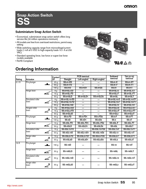
Snap Action Switch SS95Subminiature Snap Action Switch•Economical, subminiature snap action switch offers long service life (30 million operations minimum)•All models are free from overtravel restrictions, permit easy setting•Wide switching capacity range from microvoltage/current loads (1 mA at 5 VDC to high-capacity loads 10.1 A at 250 VAC)•Standard operating force, low force or super-low force models available •RoHS CompliantOrdering InformationRatingActuator Contact OF PCB terminalSoldered terminal Tab (#110) terminal Straight Left-angled Right-angled0.1 APin plunger25 g SS-01-ED ——SS-01-E SS-01-ET 50 g SS-01-FD ——SS-01-F SS-01-FT 150 gSS-01D SS-01D1SS-01D2SS-01SS-01T Hinge lever8 g SS-01GL-ED ——SS-01GL-E SS-01GL-ET 16 g SS-01GL-FD ——SS-01GL-F SS-01GL-FT 50 gSS-01GLD SS-01GLD1SS-01GLD2SS-01GL SS-01GLT Simulated roller lever 8 g SS-01GL13-ED ——SS-01GL13-E SS-01GL13-ET 16 g SS-01GL13-FD ——SS-01GL13-F SS-01GL13-FT 50 g SS-01GL13D ——SS-01GL13SS-01GL13T Hinged roller lever8 g SS-01GL2-ED ——SS-01GL2-E SS-01GL2-ET 16 g SS-01GL2-FD ——SS-01GL2-F SS-01GL2-FT 50 g SS-01GL2D ——SS-01GL2SS-01GL2T 5 APin plunger 50 g SS-5-FD SS-5-FD1SS-5-FD2SS-5-F SS-5-FT 150 g SS-5D SS-5D1SS-5D2SS-5SS-5T Hinge lever 16 g SS-5GL-FD SS-5GL-FD1SS-5GL-FD2SS-5GL-F SS-5GL-FT 50 g SS-5GLD SS-5GLD1SS-5GLD2SS-5GL SS-5GLT Simulated roller lever 16 g SS-5GL13-FD —SS-5GL13-FD2SS-5GL13-F SS-5GL13-FT 50 g SS-5GL13D SS-5GL13D1SS-5GL13D2SS-5GL13SS-5GL13T Hinge roller lever16 g SS-5GL2-FD SS-5GL2-FD1SS-5GL2-FD2SS-5GL2-F SS-5GL2-FT 50 g SS-5GL2D SS-5GL2D1SS-5GL2D2SS-5GL2SS-5GL2T 10 APin plunger 150 g SS-10D ——SS-10SS-10T Hinge lever 50 g SS-10GLD ——SS-10GL SS-10GLT Simulated roller lever 50 gSS-10GL13D——SS-10GL13SS-10GL13THinge roller lever50 g SS-10GL2D ——SS-10GL2SS-10GL2T96Snap Action Switch SSModel Number LegendSpecifications■CharacteristicsNote:1.Data shown are of initial value.2.The dielectric strength values shown is measured using a separator between the switch and metal mounting plate.3.For pin plunger models, the above value apply for use at the free position and total travel position. For the lever models, the values apply at the total travel position.Operating speed 0.1 mm to 1 m/second (pin plunger models)Operating frequency Mechanical: 400 operations per minute max.Electrical: 30 operations per minute max.Insulation resistance 100 M Ω at 500 VDC Contact resistance150 gf:SS-10, SS-5 models:30 m Ω max.SS-01 models:50 m Ω max.50 gf:SS-5 models:50 m Ω max.SS-01 models 100 m Ω max.25 gf:SS-01 models150 m Ω max.Dielectric strength (See note 2)1,000 VAC (600 VAC for SS-01), 50/60 Hz for 1 minute between terminals of same polarity1,500 VAC, 50/60 Hz for 1 minute between current-carrying metal parts and ground and between each terminal and noncurrent-carrying metal parts Vibration resistance (see note 3)Malfunction: 10 to 55 Hz, 1.5 mm double amplitude Shock resistance (see note 3)150 gf: Destruction: 1,000 m/s 2 (approx. 100G) max.Malfunction: 300 m/s 2 (approx. 30G) max.50 gf and 25gf:Destruction: 500 m/s 2 (approx. 50G) max.Malfunction: 200 m/s 2 (approx. 20G) max.Degree of protectionIEC IP40Degree of protection against electric shockClass I Proof tracking index (PTI)175Ambient operating temperature -25° to 85°C (at 60% RH max.) with no icing Ambient operating humidity 85% max. (for 5°C to 35°C)Service lifeMechanical:30 million operations min. at 60 operations per minute (SS-01, SS-5)10 million operations min. at 60 operations per minute (SS-10)Electrical:200,000 operations min. at 30 operations per minute (SS-01, SS-5)50,000 operations min. at 30 operations per minute (SS-10)WeightApprox. 1.6 g pin plunger typeSnap Action Switch SS97■Ratings (reference values)Note:1.Data in parentheses apply to the SS-10 models only.2.The above current ratings are the values of the steady-state current.3.Inductive load has a power factor of 0.4 min. (AC) and a time constant of 7 ms max. (DC). The inductive load rating of the SS-10 is the same as that of SS-5.mp load has an inrush current of 10 times the steady-state current5.Motor load has an inrush current of 6 times the steady-state current.6.If the switch is used in a DC circuit and is subjected to inrush current or surge, connect a surge suppressor across the switch.7.The electrical rating applies under the following test conditions:Ambient T emperature = 20±2°C, Ambient Humidity = 65±5%, Operating frequency = 30 operations/minute■Approved StandardsUL Recognized (File No. E41515) CSA Certified (File No. LR21642)EN61058-1 - - VDE approval(File No. 129246 for SS-5, 125256 for SS-10)EN61058-1 - - TÜV Rheinland approval (File No. J9451450)T esting conditions: 5E4 (50,000 operations), T85 (0°C to 85°C)Note:The rated values approved by each of the safety standards(e.g. UL, CSA) may be different from the performance charac-teristics individually defined in this catalog.■Contact SpecificationsNote:Minimum applicable loads are indicated by N standard refer-ence values. This value represents the failure rate at a 60%(λ60) reliability level (JIS C5003).The equation λ60=0.5 x 10⁻⁶ / operations indicates that a failure rate of 1/2,000,000 operations can be expected at a reliability level of 60%Switch series:Contact form SS-10 and SS-5SS-01Resistive loadLamp loadInductive load Motor load Resistive LoadNCNONC NO NCNONC NO NCNO125 VAC 5 A (10.1A) 1.5 A 0.7 A 3 A 2.5 A 1.3 A 0.1 A 250 VAC 3 A (10.1A) 1 A0.5 A2 A1.5 A0.8 A- - -8 VDC 5 A (10.1A) 2 A 5 A4 A 3 A 0.1 A 14 VDC5 A (10.1A)2 A 4 A3 A 0.1 A 30 VDC4 A 2 A 3 A 3 A 0.1 A 125 VDC 0.4 A 0.05 A 0.4 A 0.05 A - - -250 VDC0.2 A0.03 A0.2 A 0.03 A- - -Rated Voltage SS-10SS-5SS-01125 VAC - - - 5 A 0.1 A 250 VAC 10.1 A 3 A - - -30 VDC- - -- - -0.1 ARated Voltage SS-10SS-5250 VAC10.1 A5 ARated Voltage SS-10SS-5250 VAC10.1 A5 AItem SS-10SS-5SS-01Specification Rivet Crossbar Material Silver alloy Silver Gold alloy Gap (standard value)0.5 mm 0.25 mm Inrush current N C: 20A max.N O: 15A max.N C: 20A max.N O: 10A max.1A max.Minimum applicable load (see note)160 mA at 5 VDC 1 mA at 5 VDC98Snap Action Switch SSEngineering Data■■■MountingPanel MountingAll switches may be panel mounted using M2.3 mounting screws withplane washers or spring washers to securely mount the switch.Tighten the screws to a torque of 0.23 to 0.26 N ·m.PCB LayoutContact Form* Consult Omron for SPST -N C and SPST -N O contact form types ordering information.O v ertra v el (mm)40,00030,00020,00010,0005,0000.10.20.30.40.50.60.7Am b ient temperat u re: 20±2°CAm b ient h u midity: 65±5%W itho u t loadOperating fre qu ency: 60 operations/minS w itching c u rrent (A)5,0003,0001,00050030010050301001234567125 V AC250 V ACAm b ient temperat u re: 20±2°C Am b ient h u midity: 65±5%Operating fre qu ency: 30 operations/min cos φ = 1T w o, 2.4-dia. mo u nting holes or M2.3 scre w holes9.5 ± 0.1Three, 1.35 to 1.5 dia.8.8+0.15–0.05(1.6)16.1±0.1SPST-NCSPST-NOCOM NC COM NO NC COM NOSnap Action Switch SS99Dimensions■TerminalsNote:1.Unless otherwise specified, all units are in millimeters and a tolerance of ±0.4 mm applies to all dimensions2.T erminal plate thickness is 0.5 mm for all models.■Dimensions and Operating CharacteristicsNote:1.Unless otherwise specified, all units are in millimeters and a tolerance of ±0.4 mm applies to all dimensions2.The following illustrations and dimensions are for solder terminal models.Refer to “Terminals” for models with quick-connect terminals (#110) or PCB terminals.3.Terminal plate thickness is 0.5 mm for all models.PCB TerminalsNO terminalNC terminalNO terminalNC terminalNO terminalNC terminal8.87.39.5±0.119.83.30.60.53.28.87.39.5±0.119.83.26.48.87.39.5±0.119.83.22.35+0.075–0.05dia. holes2.35+0.075–0.05Three, 1.6 dia.10.29.57.52PTOP 6.42.92.5 1.68.87.35.119.82.5±0.07 dia.3.26.43.26.49.5±0.1ACharacteristics Part numberSS-01-E SS-01-F, SS-5-F SS-01, SS-5SS-10OF max.25 g 50 g 150 g 150 g RF min. 2 g 4 g 25 g 25 g PT max.0.5 mm 0.5 m 0.5 mm 0.6 mm OT min.0.5 mm 0.5 mm 0.5 mm 0.4 mm MD max.0.1 mm 0.1 mm 0.1 mm0.12 mmOP8.4 ± 0.5 mm100Snap Action Switch SSSS-10GL2.35+0.075–0.05Three, 1.6 dia.t = 0.3(see note 1) 2.35+0.075–0.05dia. holes6.43.26.43.614.5 (see note 2)FPOP10.29.52.5±0.07 dia.2.52.98.87.35.1Note: 1.Stainless-steel le 2.Besides the SS-GL models w ith a hinge le v er length of 14.5, the SS-GL11 models w ith a hinge le v SS-GL111 models ith a hinge le v er length of 22.6, and the SS-GL1111 models w ith a hinge le v er length of 37.Contact yo r OMRON representati v e for these models19.89.5±0.11.6ACharacteristics SS-01GL-E SS-01GL-F, SS-5GL-F SS-01GL, SS-5GL SS-10GL OF max.8 g 16 g 50 g 50 g RF min.1 g 2 g 6 g 6 g OT min. 1.2 mm 1.2 mm 1.2 mm 1.0 mm MD max.0.8 mm 0.8 mm 0.8 mm 1.0 mm FP max.13.6 mm OP 8.8 ± 0.8 mmSimulated Roller Lever Models2.35+0.075–0.05Three, 1.6 dia.2.35+0.075–0.05dia. holes1.3Rt = 0.3 (see note)2.5±0.07 dia.FPOP10.29.5 6.43.26.43.68.87.35.115.82.52.9Note:Stainless-steel spring le 19.89.5±0.11.6A Characteristics SS-10GL13-E SS-10GL13-F, SS-5GL13-F SS-01GL13, SS-5GL13SS-10GL13OF max.8 g 16 g 50 g 50 g RF min.1 g 2 g 6 g 6 g OT min. 1.2 mm 1.2 mm 1.2 mm 1.0 mm MD max.0.8 mm 0.8 mm 0.8 mm 1.0 mm FP max.15.5 mm OP 10.7±0.8 mme Roller Lever ModelsSS-10GL2Three, 1.6 dia.2.35+0.075–0.05dia. 2.35+0.075–0.05dia. holes4.8 dia. (see note 2)Note:1.Stainless-steel spring le2.Polyacetal resin roller2.5±0.07 dia.t = 0.3(see note 1)2.52.914.5FPOP10.29.5 6.48.87.35.119.83.26.49.5±0.11.6ACharacteristics SS-01GL2-E SS-01GL2-F, SS-5GL2-F SS-01GL2, SS-5GL2SS-10GL2OF max.8 g 16 g 50 g 50 g RF min.1 g 2 g 6 g 6 g OT min. 1.2 mm 1.2 m 1.2 mm 1.0 mm MD max.0.8 mm 0.8 mm 0.8 mm 1.0 mm FP max.19.3 mm OP 14.5 ± 0.8 mmSnap Action Switch SS101PrecautionsBe sure to read the precautions and information common to all Snap Action and Detection Switches, contained in the T echnical User’s Guide, “Snap Action Switches, Technical Information” for correct use.■Correct UseMountingMount the switch onto a flat surface. Mounting on an uneven surface may cause deformation of the switch, resulting in faulty operation or breakage in the housing.Operating StrokeT ake particular care in setting the operating stroke for the pin plunger models. Make sure that the operating stroke is 70% to 100% of the rated OT distance. Do not operate the actuator exceeding the OT dis-tance, otherwise the life expectancy of the switch may be shortened.Using MicroloadsUsing a model for ordinary loads to switch microloads may result in faulty operation. Instead, use the models that are designed for microloads and that operate in the following range;However, even when using microload models within the operating range shown above, if inrush current or inductive voltage spikes occur when the contact is opened or closed, then contact wear may increase and so decrease the service life. Therefore, insert a contact protection circuit where necessary.■CautionsHandlingTurn OFF the power supply before mounting or removing the switch,wiring, or performing maintenance for inspection. Failure to do so may result in electric shock or burningTerminal ConnectionWhen soldering the lead wire to the terminal, first insert the lead wire conductor through the terminal hole and then solder.Make sure that the capacity of the soldering iron is 60 W maximum.Do not take more than 5 seconds to solder the switch terminal.Improper soldering involving an excessively high temperature or excessive soldering time may deteriorate the characteristics of the switch.Be sure to apply only the minimum required amount of flux. The switch may have contact failures if flux intrudes in the interior of the switch.Use the following lead wires to connect to the solder terminals;If the PCB terminal models are soldered in a solder bath, flux will per-meate inside the switch and cause contact failure. Therefore, manu-ally solder the PCB terminal.Wire the quick-connect terminals (#110) with receptacles. Insert the terminals straight into the receptacles. Do not impose excessive force on the terminal in the horizontal direction, otherwise the termi-nal may be deformed or the housing may be damaged.Insulation DistanceUse a separator between the switch and metal mounting panels, to ensure proper dielectric characteristics are achieved.According to E N 61058-1, the minimum insulation thickness for this switch should be 1.1 mm and minimum clearance distance between the terminal and mounting plate should be 1.6 mm. If the insulation distance cannot be provided in the product incorporating the switch,either use a switch with insulation barrier or use a separator toensure sufficient insulation distance.Operating range for micro load models SS-01Operating range for general-load modelsSS-5, SS-10C u rrent (mA)V o l t a g e (V )Inopera b le range 3024121,0001001015100mA100mA 160mA26mA 1mA0.16mA Model Conductor size SS-50.5 to 0.75 mm 2SS-100.75 mm 2Snap Action Switch SSOMRON ON-LINEGlobal - USA - Cat. N o. X303-E-1Printed in USAOMRON ELECTRONIC COMPONENTS LLC55 E. Commerce Drive, Suite B Schaumburg, IL 60173847-882-228811/10 Specifications subject to change without noticeAll sales are subject to Omron Electronic Components LLC standard terms and conditions of sale, which can be found at /components/web/webfiles.nsf/sales_terms.html ALL DIMENSIONS SHOWN ARE IN MILLIMETERS.T o convert millimeters into inches, multiply by 0.03937. T o convert grams into ounces, multiply by 0.03527.分销商库存信息:OMRONSS-01GL111SS-01GL111D SS-5GLD-12SS-01GL30PT SS-5GL11SS-5GL111SS-5GL1375-3T BY OMI SS-5GL111-F SS-5GL111TSS-5GL1111T BY OMI SS-5GL111-FT SS-5GL1131TSS-5GL1131SS-5GL1140-3SS-5GL1138 BY OMI SS-5GL1112T SS-01GL1131SS-5GL111-FDSS-5GL1129D SS-5GL1144D SS-01GL111-FTSS-5GL1111D2SS-01GL111-E SS-5GL1111SS-01GL11SS-01GL11-F SS-5GL111-FD2SS-01GL1131-ET SS-01GL1140T SS-5GL111D1SS-01GL1111D SS-01GL111T SS-01GL111-ED1 SS-5GL111-FD1SS-01GL111-ED SS-01GL111-ETSS-01GL111-FD1SS-5GL1170-3SS-1-4。
Q130B说明书J10IL1 Series Simplified Chinese

序言Copyright 2008版权所有、翻印必究本文件的信息如有关于可靠性、设计和功能提高方面的改变,恕不另行通知,本文件的信息并不表示制造商方面的承诺。
制造商绝不就因使用或不能使用本产品或文件所发生直接的、间接的、特殊的、意外的或因此导致的损害而承担赔偿责任,即使事先被告知该损害发生的可能性。
本文件包含受版权保护的所有权信息。
版权所有。
未经制造商的书面许可,严禁以任何形式,或通过任何机械、电子或其它方法,复制本手册中的任何部分。
声明虽然本手册努力做到准确无误,但制造商和分销商对因本手册的错误或疏忽,或因使用本手册中包含的信息而导致的损失不承担赔偿责任。
i目录在您开始前-------------------------------------------------------------------2本手册使用说明---------------------------------------------------------------2安全预防措施------------------------------------------------------------------2在您开始使用电脑前必须要熟记的事项---------------------------------5合适的工作位置---------------------------------------------------------------5介紹----------------------------------------------------------------------------7準備您的电脑------------------------------------------------------------------7熟悉您的电脑------------------------------------------------------------------8开始---------------------------------------------------------------------------14连接电源-----------------------------------------------------------------------14开启笔记本电脑--------------------------------------------------------------15利用电池的电量操作电脑--------------------------------------------------15使用笔记本电脑------------------------------------------------------------18 LCD屏幕的显示-------------------------------------------------------------18功能键(快速键)-----------------------------------------------------------19触控面板-----------------------------------------------------------------------20连接外接的磁道装置--------------------------------------------------------20省电模式-----------------------------------------------------------------------21重新设定系统-----------------------------------------------------------------23使用 Windows----------------------------------------------------------------23网络连接---------------------------------------------------------------------29使用无线局域网连接到互联网--------------------------------------------29使用有线局域网连接互联网-----------------------------------------------30运行BIOS设置------------------------------------------------------------32进入次选单--------------------------------------------------------------------33一般辅助说明-----------------------------------------------------------------33系统恢复-----------------------------------------------------------------------38 VGA 公用程序-------------------------------------------------------------42 3G 连接----------------------------------------------------------------------48疑难排解---------------------------------------------------------------------52音频问题-----------------------------------------------------------------------53硬盘问题-----------------------------------------------------------------------53显示问题-----------------------------------------------------------------------54ii键盘和鼠标问题--------------------------------------------------------------55 CMOS电池问题--------------------------------------------------------------55内存问题-----------------------------------------------------------------------56 PC卡问题---------------------------------------------------------------------56性能问题-----------------------------------------------------------------------57 USB2.0问题-------------------------------------------------------------------57規格---------------------------------------------------------------------------59iii注意事项交通委员会射频干扰声明经测试本设备符合“FCC 规则”第 15 部分中 B 类数字设备的限制。
MOV-14D201K,MOV-14D431K,MOV-14D471K,MOV-14D181K,MOV-14D391K,MOV-14D511K, 规格书,Datasheet 资料
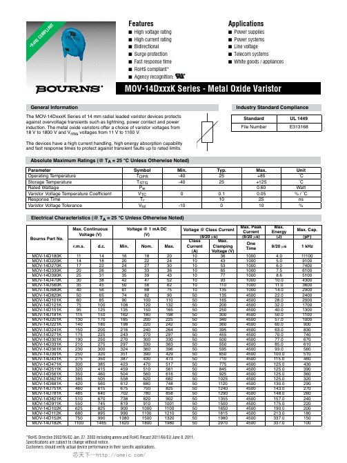
*RoHS Directive 2002/95/EC Jan. 27, 2003 including annex and RoHS Recast 2011/65/EU June 8, 2011. Specifi cations are subject to change without notice.Customers should verify actual device performance in their specifi c applications.Absolute Maximum Ratings (@ T A = 25 °C Unless Otherwise Noted)ParameterSymbol Min.Typ.Max.Unit Operating Temperature T OPR -4025+85˚C Storage Temperature T STG -4025+125˚C Rated WattageP w 0.60Watt Varistor Voltage Temperature Coeffi cient V TC 00.10.05 % / ˚C Response TimeT r 1025ns Varistor Voltage ToleranceV tol-1010%Electrical Characteristics (@ T A = 25 °C Unless Otherwise Noted)*Ro H S C O MP L I A N TBourns Part No.Max. Continuous Voltage (V)Voltage @ 1 mA DC(V)Voltage @ Class Current Max. PeakCurrent Max.Energy Max. Cap.(8/20 μs)(8/20 μs)(J)(pF)r.m.s.d.c.Min.Nom.Max.ClassCurrent(A)Max.Clamping Voltage (V)One Time 8/20 μs 1 kHz MOV-14D180K 111416182010361000 4.011100MOV-14D220K 141820222410431000 5.09100MOV-14D270K 172224273010531000 6.07400MOV-14D330K 2026303336106510007.56100MOV-14D390K 2531353943107710008.65100MOV-14D470K 30384247521093100010.04300MOV-14D560K 354550566210110100011.03600MOV-14D680K 405661687510135100014.02900MOV-14D820K 506574829050135450022.02400MOV-14D101K 60859010011050165450028.02000MOV-14D121K 7510010812013250200450032.01700MOV-14D151K 9512513515016550250450040.01300MOV-14D181K 11515016218019850300450050.01100MOV-14D201K 13017018520022550340450057.01000MOV-14D221K 14018019822024250360450060.0900MOV-14D241K 15020021624026450395450063.0830MOV-14D271K 17522524327029750455450070.0740MOV-14D301K 19025027030033050500450077.0670MOV-14D331K 21027529733036350550450085.0610MOV-14D361K 23030032436039650595450093.0560MOV-14D391K 250320351390429506504500100.0510MOV-14D431K 275350387430473507104500115.0460MOV-14D471K 300385423470517507754500125.0430MOV-14D511K 320415459510561508454500125.0390MOV-14D561K 350460504560616509254500125.0360MOV-14D621K 3855055586206825010254500125.0320MOV-14D681K 4205606126807485011204500130.0290MOV-14D751K 4606156757508255012404500143.0270MOV-14D781K 4856407027808585012904500148.0260MOV-14D821K 5106707388209025013554500157.0240MOV-14D911K 55074581991010015015004500175.0220MOV-14D102K 625825900100011005016504500190.0200MOV-14D112K 680895990110012105018154500213.0180MOV-14D152K 7509901080150013205019804500337.0150MOV-14D182K110014651620180019805029704500337.010014D 201K5Specifi cations are subject to change without notice.Customers should verify actual device performance in their specifi c applications.Product DimensionsDIMENSIONS:MM(INCHES)This is an RoHS compliant molded radial package with 100 % Sn plating on the terminations.Internal ConstructionHow to OrderMOV - 14D nn (n) K (TR)Model DesignatorMOV = Metal Oxide Varistor Disc Diameter 14D = 14 mmNominal Varistor VoltageSee Electrical Characteristics TableMultiplier of Voltage Digits 0 = No multiplier 1 = nn * 101 2 = nn * 102Varistor Voltage Tolerance K = 10 %PackagingBlank = BulkTR = Tape & Reel*Examples: MOV-14D270K = 27 V, Bulk PackMOV-14D331KTR = 330 V, T ape & Reel* Models MOV-14D911K, 102K, 112K, 152K and 182K are not available in Tape & Reel packaging.Part Number Dim. H (Max.)Dim. T (Max.)MOV-14D180K20.0(.787) 3.8(.150)MOV-14D220K 20.0(.787) 3.9(.154)MOV-14D270K 20.0(.787) 4.2(.165)MOV-14D330K 20.0(.787) 3.8(.150)MOV-14D390K20.0(.787) 4.0(.157)MOV-14D470K 20.0(.787) 4.2(.165)MOV-14D560K 20.0(.787) 4.3(.169)MOV-14D680K 20.0(.787) 4.4(.173)MOV-14D820K20.0(.787) 3.8(.150)MOV-14D101K 20.0(.787) 4.0(.157)MOV-14D121K20.0(.787) 4.2(.165)MOV-14D151K 20.0(.787) 4.4(.173)MOV-14D181K20.0(.787) 3.6(.142)MOV-14D201K 20.0(.787) 3.8(.150)MOV-14D221K 20.0(.787) 3.9(.154)MOV-14D241K 20.0(.787) 4.0(.157)MOV-14D271K 20.0(.787) 4.2(.165)MOV-14D301K20.0(.787) 4.4(.173)Part Number Dim. H (Max.)Dim. T (Max.)MOV-14D331K 20.0(.787) 4.6(.181)MOV-14D361K 20.0(.787) 4.8(.189)MOV-14D391K 20.0(.787) 5.0(.197)MOV-14D431K 20.0(.787) 5.2(.205)MOV-14D471K 20.0(.787) 5.4(.213)MOV-14D511K 20.0(.787) 5.5(.217)MOV-14D561K 22.0(.866) 6.0(.236)MOV-14D621K 22.0(.866) 6.4(.252)MOV-14D681K 22.0(.866) 6.5(.256)MOV-14D751K 22.0(.866) 6.7(.264)MOV-14D781K 22.0(.866) 6.9(.272)MOV-14D821K 22.0(.866)7.3(.287)MOV-14D911K*22.0(.866)7.7(.303)MOV-14D102K*22.0(.866)8.2(.323)MOV-14D112K*22.0(.866)8.7(.343)MOV-14D152K*22.0(.866)9.7(.382)MOV-14D182K*22.0(.866)11.7(.461)* Not available in Tape & Reel packaging.Specifi cations are subject to change without notice.Customers should verify actual device performance in their specifi c applications.1011001000101010101010Current (A)V o l t a g e (V )680560470390330270220180100100010000101010101010Current (A)V o l t a g e (V )18215211210291182178175168162156151147110010100010000101010101010Current (A)V o l t a g e (V )431391361331301271241221201181151121101820101010101010101010101010101010Performance Graphs V-I CharacteristicsMOV-14D180K to MOV-14D680KMOV-14D820K to MOV-14D431KMOV-14D471K to MOV-14D182KBournsPart Number Bourns Part Marking MOV-14D180K 14D180K MOV-14D220K 14D220K MOV-14D270K 14D270K MOV-14D330K 14D330K MOV-14D390K 14D390K MOV-14D470K 14D470K MOV-14D560K 14D560K MOV-14D680K 14D680K MOV-14D820K 14D820K MOV-14D101K 14D101K MOV-14D121K 14D121K MOV-14D151K 14D151K MOV-14D181K 14D181K MOV-14D201K 14D201K MOV-14D221K 14D221K MOV-14D241K 14D241K MOV-14D271K 14D271K MOV-14D301K 14D301K MOV-14D331K 14D331K MOV-14D361K 14D361K MOV-14D391K 14D391K MOV-14D431K 14D431K MOV-14D471K 14D471K MOV-14D511K 14D511K MOV-14D561K 14D561K MOV-14D621K 14D621K MOV-14D681K 14D681K MOV-14D751K 14D751K MOV-14D781K 14D781K MOV-14D821K 14D821K MOV-14D911K 14D821K MOV-14D102K 14D102K MOV-14D112K 14D112K MOV-14D152K 14D152K MOV-14D182K14D182KNOTE: The “5” marking on MOV products is for traceability of production assembly for quality assurance compliance.Typical Part MarkingPackaging InformationTAPE & REELItem Symbol14 mm Disc Reel Outside Diameter RD355(13.98) Reel Inner Diameter RD130(11.81) Tape Width RW55(2.165) Reel Width RW163(2.48) Pitch of Component P25.4 ± 1.0(1.00 ± 0.04) Feed Hole Pitch P012.7 ± 1.0(0.50 ± 0.04) Feed Hole Center to Pitch P18.95 ± 0.7(0.352 ± 0.3) Feed Hole Center to ComponentCenterP212.7 ± 1.0(0.50 ± 0.04)Lead to Lead Distance F7.50 ± 0.8(0.30 ± 0.03)Component AlignmentΔh4.0max.(0.157) max.Tape Width W18.0 ± 0.5(0.71 ± 0.02)Hole Down Tape Width W012.0 ± 0.8(0.47 ± 0.03)Hole Position W19.0 ± 0.5(0.35 ± 0.02)Hole Down Tape Position W23.0max.(0.12) max.Height From Center toComponent BaseH19.0 ± 1.0(0.75 ± 0.04)Seating Plane Height H016.0 ± 0.5(0.63 ± 0.02)Component Height H140.0max.(1.57) maxCrimp Length C2.60typ.(0.10) maxFeed Hole Diameter D04.0 ± 0.2(0.16 ± 0.08)Total Tape Thickness t0.6 ± 0.3(0.02 ± 0.01)Length of Clippped Height L1.0max.(0.04) maxQuantity per ReelMOV-14D180K – 14D391KMOV-14D431K - 14D182K-100050012/11Specifi cations are subject to change without notice.Customers should verify actual device performance in their specifi c applications.BULK60.0(2.36)Asia-Pacifi c:Tel: +886-2 2562-4117Fax: +886-2 2562-4116Europe:Tel: +41-41 768 5555Fax: +41-41 768 5510The Americas:Tel: +1-951 781-5500Fax: +1-951 781-5700NOTE: Models MOV-14D911K, 102K, 112K, 152K and 182K are not availablein Tape & Reel packaging.。
SCALANCE X101-1 商品说明书
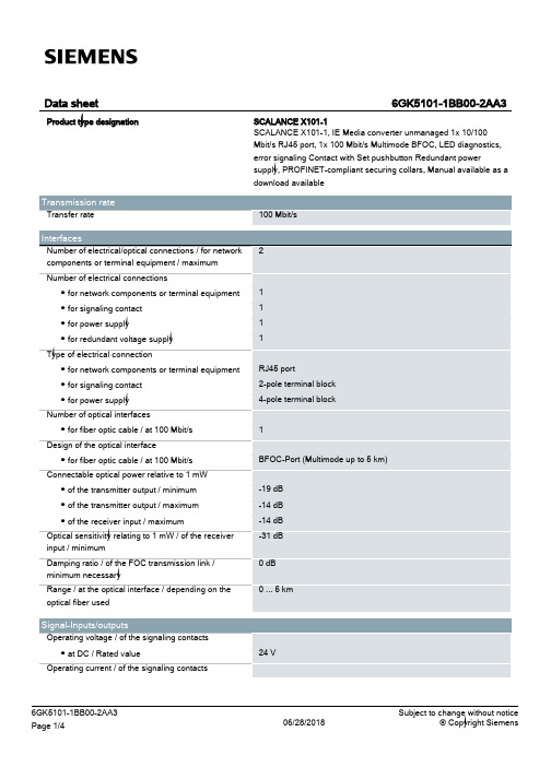
24 V
6GK5101-1BB00-2AA3 Page 1/4
06/28/2018
Subject to change without notice © Copyright Siemens
● at DC / maximum
Supply voltage, current consumption, power loss Supply voltage ● external ● external Type of voltage / of the supply voltage Product component / fusing at power supply input Fuse protection type / at input for supply voltage Consumed current ● maximum Power loss [W] ● at DC / at 24 V
Compact 40 mm 125 mm 124 mm 0.55 kg
Yes Yes Yes
No No
FM3611: Class 1, Divison 2, Group A, B, C, D / T.., Class 1, Zone 2, Group IIC, T.. EN 600079-15 II 3 G EEx nA II T.. KEMA 06 ATEX 0021 X
Yes
Yes Yes Yes Yes Yes No 134 y
/snst
/simatic-net https:// /industry/infocenter /bilddb /cax https://
Security information
UL 60950-1, CSA C22.2 No. 60950-1 UL 1604 and UL 2279-15 (Hazardous Location), Class 1 / Division 2 / Group A, B, C, D / T.., Class 1 / Zone 2 / Group IIC / T.. EN 61000-6-3 EN 61000-6-4:2001 EN 61000-6-2:2001, EN 61000-6-4:2001 Yes Yes Yes
D R I L L S 2001年版商品目录说明书

D R I L L S2001N O T E SiI N D E XFractional Sizes,118°Point,Surface Treated . . . . . . . . . . . . . . . .1600 . . . . .1Fractional Diameters,118°Point,Bright .1600 . . . . .1Fractional Diameters,118°Point,TiN Coated . . . . . . . . . . . . . . . . . . . .1600 . . . . .1Wire Sizes,118°Point,Surface Treated .1601 . . . . .2Wire Sizes,118°Point,Bright . . . . . . . .1601 . . . . .2Wire Sizes,118°Point,TiN Coated . . . . .1601 . . . . .2Letter Sizes,118°Point,Surface Treated .1602 . . . . .3Letter Sizes,118°Point,Bright . . . . . . .1602 . . . . .3Letter Sizes,118°Point,TiN Coated . . . .1602 . . . . .3Metric Sizes,118°Point,Surface Treated 1603 . . . .4–6Metric Sizes,118°Point,Bright . . . . . . .1603 . . . .4–6J O B B E R S L E N G T H , H E A V Y D U T YHigh Speed SteelFractional Sizes,135°Split Point,Surface Treated . . . . . . . . . . . . . . . .1604 . . . . .7Fractional Diameters,135°Split Point,TiN Coated . . . . . . . . . . . . . . . . . . . .1604 . . . . .7Wire Sizes,135°Split Point,Surface Treated . . . . . . . . . . . . . . . .1605 . . . . .8Wire Sizes,135°Split Point,TiN Coated .1605 . . . . .8Letter Sizes,135°Split Point,Surface Treated . . . . . . . . . . . . . . . .1605-A . . . .9Letters Sizes,135°Split TiN Coated . . .1605-A . . . .9CobaltFractional Sizes,135°Split Point,Surface Treated . . . . . . . . . . . . . . . .1606 . . . .10Wire Sizes,135°Split Point,Surface Treated . . . . . . . . . . . . . . . .1607 . . . .11Letter Sizes,135°Split Point,Surface Treated . . . . . . . . . . . . . . . .1608 . . . .12Fractional Sizes,118°Point,Surface Treated . . . . . . . . . . . . . . . .1609 . . .13–14Fractional Sizes,118°Point,Bright . . . . .1609 . . .13–14Wire Sizes,118°Point,Surface Treated .1610 . . . .15Letter Sizes,118°Point,Bright . . . . . . .1611 . . . .16S C R E W M A C H I N E L E N G T H S , H E A V Y D U T YHigh Speed SteelFractional Sizes,135°Split Point,Surface Treated . . . . . . . . . . . . . . . .1612 . . . .17Fractional Sizes,135°Split Point,TiN Coated . . . . . . . . . . . . . . . . . . . .1612 . . . .17Wire Sizes,135°Split Point,Surface Treated . . . . . . . . . . . . . . . .1613 . . . .18Wire Sizes,135°Split Point,TiN Coated .1613 . . . .18Letter Sizes,135°Split Point,Surface Treated . . . . . . . . . . . . . . . .1614 . . . .19CobaltFractional Sizes,135°Split Point,Surface Treated . . . . . . . . . . . . . . . .1615 . . . .20Wire Sizes,135°Split Point,Surface Treated . . . . . . . . . . . . . . . .1616 . . . .21Letter Sizes,135°Split Point,Surface Treated . . . . . . . . . . . . . . . .1617. . . .22R E D U C E D S H A N KHigh Speed Steel1/2" Round Shank S &D,118°Point,Surface Treated . . . . . . . . . . . . . . . .1618 . . . .23S E T SDrill Sets . . . . . . . . . . . . . . . . . . . . . . . . .1619 . . .24–25LIST STYLENO.PAGE Drill Feeds And Speeds . . . . . . . . . . . . . . . . . . . . . . . .30Trouble Shooting Guide . . . . . . . . . . . . . . . . . . . . . . . .31Tap Drill Sizes For Metric Screw Threads . . . . . . . . . . .34Hardness Conversion Table . . . . . . . . . . . . . . . . . . . . .35LIST STYLENO.PAGEI N D E XSurface TreatedTiN Coatedii1J O B B E R S L E N G T H , H I G H S P E E D S T E E LG E N E R A L P U R P O S E , J O B B E R S L E N G T H D R I L L118°P o i n t , S u r f a c e T r e a t e d , B r i g h t , o r T i N C o a t e dG E N E R A L F E A T U R E S A N D A P P L I C A T I O N SDesigned for portable and machine drilling in a broad range of steel,ferrous and non-ferrous materials (bright finish in non-ferrous),under many different conditions.TiN coating with increased surface hardness allows for extended tool life,greater lubricity,betterchip ejection,increased productivity,and lower horsepower requirements.J O B B E R S L E N G T H , H I G H S P E E D S T E E L2J O B B E R S L E N G T H , H I G H S P E E D S T E E L3L e t t e r S i z e sG e n e r a l P u r p o s e , 118°P o i n tP A C K A G I N GA to N — 12 per package O to Z — 6 per packageEDP NO.EDP NO.J O B B E R S L E N G T H , H I G H S P E E D S T E E L4c o n t i n u e dM E T R I C , J O B B E R S L E N G T H D R I L L118°P o i n t (M a n u f a c t u r e d t o D I N S t a n d a r d s ),B r i g h t F i n i s h t o .50, S u r f a c e T r e a t e d .55 a n d L a r g e rG E N E R A L F E A T U R E S A N D A P P L I C A T I O N SDesigned for portable and machine drilling in a broad range of steel,ferrous and non-ferrous materials (bright finish in non-ferrous),under many different conditions.TiN coating with increased surface hardness allows for extended tool life,greater lubricity,better chip ejection,increased productivity,and lower horsepower requirements.J O B B E R S L E N G T H , H I G H S P E E D S T E E L5c o n t i n u ed Me t r i c S i z e sG e n e r a l P u r p o s e , 118°P o i n tFLUTE LENGTHOVERALL LENGTH EDP NO.c o n t i n u ed FLUTE LENGTH OVERALL LENGTH EDP NO.c o n t i n u e dJ O B B E R S L E N G T H , H I G H S P E E D S T E E L6J O B B E R S L E N G T H , H I G H S P E E D S T E E LM E D I U M D U T Y , J O B B E R S L E N G T H D R I L L135°S p l i t P o i n t , S u r f a c e T r e a t e d o r T i N C o a t e dG E N E R A L F E A T U R E S A N D A P P L I C A T I O N SMedium duty aircraft type B drills are designed for more demanding applications.The 135°split point is self-centering,reduces thrust is quick start-ing and highly accurate.ideal for portable or machine drilling of low tensile strength alloy material and stainless steels.TiN coating with increased surface hardness allows for extended tool life,greater lubricity,better chip ejection,increased productivity,and lower horsepower requirements.J O B B E R S L E N G T H,H I G H S P E E D S T E E LJ O B B E R S L E N G T H,H I G H S P E E D S T E E LH E A V Y D U T Y,J O B B E R S L E N G T H D R I L L135°S p l i t P o i n t,S t r a w F i n i s hG E N E R A L F E A T U R E S A N D A P P L I C A T I O N SHeavy duty aircraft type J drills are designed for tough,high tensile strength materials such as PH stainless steel, titanium,and inconel.The heat resistant cobalt material in combination with the 135°degree self-centering split point reduces thrust,is quick starting and highly accurate.Ideal for machine drilling.J O B B E R S L E N G T H,C O B A L T H I G H S P E E D S T E E LS C R E W M A C H I N E L E N G T H , H I G H S P E E D S T E E Lc o n t i n u e dG E N E R A L P U R P O S E , S C R E W M A C H I N E L E N G T H D R I L L H i g h S p e e d S t e e l , 118°P o i n t , S u r f a c e T r e a t e dG E N E R A L F E A T U R E S A N D A P P L I C A T I O N SPrimarily used in screw machines.Shorter flute and overall length provides increase rigidity in machine drilling resulting in lessdeflection,increased tool life,and better hole accuracy.Designed to drill in a wide variety of low tensile strength materials.S C R E W M A C H I N E L E N G T H,H I G H S P E E D S T E E LS C R E W M A C H I N E L E N G T H,H I G H S P E E D S T E E LS C R E W M A C H I N E L E N G T H,H I G H S P E E D S T E E LS C R E W M A C H I N E L E N G T H , H I G H S P E E D S T E E LH E A V Y D U T Y , S C R E W M A C H I N E L E N G T H D R I L L 135°S p l i t P o i n t , S u r f a c e T r e a t e d o r T i N C o a t e dG E N E R A L F E A T U R E S A N D A P P L I C A T I O N SHeavy duty,aircraft type C drills are ideal for portable drilling.The 135°split point is self-centering,reduces thrust,and is quick starting.The short rugged constructions performs will in a broad range of materials in the iron and steel families.TiN coating with increased surface hardness allowsfor extended tool life,greater lubricity,better chip ejection,increased productivity,and lower horsepower requirements.S C R E W M A C H I N E L E N G T H,H I G H S P E E D S T E E LS C R E W M A C H I N E L E N G T H,H I G H S P E E D S T E E LS C R E W M A C H I N E L E N G T H,C O B A L T H I G H S P E E D S T E E Lrugged construction performs well in a broad range of materials especially high alloys and work hardened material.T5F r a c t i o n a l S i z e sH e a v y D u t y,135°S p l i t P o i n tP A C K A G I N G1/16 to 19/64 — 12 per envelope5/16 to 1/2 — 6 per envelopeEDP NO.SIZE EQUIV.LENGTH LENGTH FINISH1/16.06255/81-5/8687005/64.078111/161-11/16687013/32.09383/41-3/4687027/64.109413/161-13/16687031/8.12507/81-7/8687049/64.140615/161-15/1668705S C R E W M A C H I N E L E N G T H,C O B A L T H I G H S P E E D S T E E LS C R E W M A C H I N E L E N G T H,C O B A L T H I G H S P E E D S T E E LR E D U C E D S H A N K D R I L L S , H I G H S P E E D S T E E L1/2 RO U N D S H A N K S & D D R I L L , R E D U C E D S H A N K D R I L LH i g h S p e e d S t e e l , 118°P o i n t , S u r f a c e T r e a t e dG E N E R A L F E A T U R E S A N D A P P L I C A T I O N SFor use in a 1/2" diameter portable drill chuck.Precision ground for a high degree of concentricity between the shank and body diameter.Ideal for drilling in low and medium tensile mon flute and overall lengths allow for minimal adjustment during tool change.S E T S118°J O B B E R S L E N G T H,G E N E R A L P U R P O S E,H I G H S P E E D S T E E L118°M E T R I C J O B B E R S L E N G T H,G E N E R A L P U R P O S E,H I G H S P E E D S T E E LS E T S135°M E D I U M D U T Y , J O B B E R S L E N G T H , H I G H S P E E D S T E E L135°H E A V Y D U T Y , J O B B E R S L E N G T H , C O B A L T H I G H S P E E D S T E E LS E T S118°G E N E R A L P U R P O S E,S C R E W M A C H I N E L E N G T H,H I G H S P E E D S T E E L135°M E D I U M D U T Y,S C R E W M A C H I N E L E N G T H,H I G H S P E E D S T E E L135°H E A V Y D U T Y,S C R E W M A C H I N E L E N G T H,C O B A L T H I G H S P E E D S T E E LS E T S27118°1/2 R E D U C E D S H A N K , H I G H S P E E D S T E E LT E C H N I C A L I N F O R M A T I O N28D RI L L N O M E N C L A T U R EAxis – The imaginary straight line which forms the longitudinal center line of the drill.Back Taper – A slight decrease in diameter from front to back in the body of the drill.Body – The portion of the drill extending from the shank or neck to the outer corners of the cutting lips.Body Diameter Clearance – That portion of the land that has been cut away so it will not rub against the walls of the hole.Chisel Edge – The edge at the end of the web that connects the cut-ting lips.Chisel Edge Angle – The angle included between the chisel edge and the cutting lip,as viewed from the end of the drill.Clearance – The space provided to eliminate undesirable contact between the drill and the workpiece.Clearance Diameter – The diameter over the cut away portion of the drill lands.Drill Diameter – The diameter over the margins of the drill measured at the point.Flutes – Helical or straight grooves in the body of the drill to provide cutting lips,permit removal of chips and allow coolant to reach the cutting lips.Flute Length – The length from the outer corners of the cutting lips to the extreme back end of the flutes.Helix Angle – The angel made by the leading edge of the land with a plane containing the axis of the drill.Land – the peripheral portion of the body between adjacent nd Width – The distance between the leading edge and the heel of the land measured at a right angle to the leading edge.Lead – The axial advance of the leading edge of the land in one turnaround the circumference.Lips – The cutting edges of a two-flute drill extending from the chisel edge to the periphery.Lip Relief – The axial relief angle at the outer corner of the lip.It is measured by projection into a plane,tangent to the periphery,at the outer corner of the lip.Margin – The cylindrical portion of the land which is not cut away to provide clearance.Overall Length – The length from the extreme end of the shank to the outer corners of the cutting lips.It does not include the conical shank end,often used on straight shank drills,or the conical cutting point.Point – The cutting end of a drill,made up of the ends of the lands and the web.In form it resembles a cone but departs from a true cone to furnish clearance behind the cutting lips.Point Angle – The angle included between the cutting lips,projected upon a plane parallel to the drill axis and parallel to the two cutting lips.Relative Lip Height – The difference in indicator reading between the cutting lips of the drill.It is measured at a right angle to the cutting lip at a specific distance from the axis of the drill.Relief –The result of the removal of tool material behind the cutting lip and leading edge of the land to provide clearance and prevent rub-bing.Web – The central portion of the body that joins the lands.The extreme end of the web forms the chisel edge on a two-flute drill.Web Thickness – The thickness of the web at the point,unless anoth-er specific location is specified.Web Thinning – The operation of reducing the web thickness,at the point,to reduce drilling thrust.T E C H N I C A L I N F O R M A T I O NS P E E D S F O R D R I L L I N GCUTTING POINTSPEED POINT ANGLEMATERIAL BEING DRILLED(SFM)STYLE(DEGREES)FEED RATE Aluminum Alloys200-300Conventional118Medium to Heavy Magnesium Alloys200-300Conventional118Medium to Heavy Brass and Bronze75-150Conventional118Medium to Heavy Cast IronSoft75-125Conv.or Split118 or 135Medium to Heavy Medium Hard50-100Conv.or Split118 or 135MediumHard Chilled10-20Conventional118Light to Medium Malleable75-125Conv.or Split118 or 135MediumSteelMild,.2 to .3 Carbon50-100Conventional118Medium to Heavy Medium,.4 to .5 Carbon45-80Conventional118MediumTool,1.2 Carbon40-60Conventional118MediumForgings40-60Conventional118MediumAlloy,300 to 400 BHN20-30Conv.or Split118 or 135MediumHigh TensileRc 35-4030-40Conv.or Split118 or 135MediumRc 40-4525-35Conv.or Split118 or 135MediumRc 45-5015-25Conv.or Split118 or 135Light to Medium Rc 50-557-15Conv.or Split118 or 135Light to Medium Maraging,Heat Treated7-20Conv.or Split118 or 135MediumMaraging,Annealed40-55Conv.or Split118 or 135Light to Medium Titanium AlloysCommercially Pure50-60Heavy Duty Split135Medium5AI-2Sn,8Al-1 Mo-1V20-45Heavy Duty Split135Medium2Fe-2Cr-Mo Annealed6Al-4V,4Al-4Mn,7Al-4Mo20-35Heavy Duty Split135Medium5Al-2Sn,8Al-1Mo-1V15-20Heavy Duty Split135Medium2Fe-2Cr-Mo SolutionTreated and AgedHigh Temperature AlloysCobalt Base,HS25,S816,V367-20Heavy Duty Split135MediumINCO 800,A286,N1557-20Heavy Duty Split135MediumNickel Base,Inconel 700,5-15Heavy Duty Split135MediumU500,Rene 41Monel Metal30-50Heavy Duty Split135Medium Stainless SteelFree Machining,303,416,42030-100Heavy Duty Split135MediumAustenitic,300 Series20-60Heavy Duty Split135MediumFerritic,400 Series20-60Heavy Duty Split135MediumMartensitic,Heat Treated10-30Heavy Duty Split135MediumPlastics and Related Materials100-200Low Angle90Medium to Heavy Zinc Alloys150-250Conventional118Medium to Heavy The speeds shown are for average conditions where coolant can be efficiently applied.Where the strength of the drill is not a critical factor and where the workpiece can be rigidly supported.When one or more of these conditions vary,the speeds must be adjusted accordingly.29T E C H N I C A L I N F O R M A T I O N30F E E D R A T E P E R R E V O L U T I O N F O R D R I L L SDRILL DIAMETER FEED PER REVOLUTIONRANGELIGHTMEDIUMHEAVY1/16 Thru 1/8.0005–.0010.0010–.0020.0020–.0030Over 1/8 Thru 1/4.0010–.0030.0030–.0050.0050–.0070Over 1/4 Thru 1/2.0030–.0050.0050–.0070.0070–.0090Over 1/2 Thru 3/4.0050–.0080.0080–.0110.0110–.0140Over 3/4 Thru 1.0080–.0110.0110–.0140.0140–.0170Over 1.0120–.0150.0150–.0200.0200–.0250The feed rates shown are for average conditions where coolant can be efficiently applied,where the strength of the drill is not a critical factor and where the workpiece can be rigidly supported.When one or more of these conditions vary; the feeds must be adjusted accordingly.S P E E D S A N D F E E D S F O R D E E P H O L E D R I L L I N GHoles which must be drilled three or more diameters deep fall into the “Deep Hole”drilling class and some adjustment of speeds and feeds is necessary.The deeper the hole,the greater the tendency for chip to pack and clog the flutes of the drill.This increases the amount of heat generated and prevents coolant from reaching the drill points.Heat buildup will eventually result in premature failure.Step drilling,that is,drilling a short distance and then retracting the drill,will often reduce the chip packing.The deeper the hole the more often the drill must be retracted.A reduction in speed and feed to reduce the amount of heat generated is generally required in most deep-hole applications where coolant cannot be effectively applied.S P E E D A N D F E E D R E D U C T I O N P E R C E N T A G E S F O R D E E P H O L E D R I L L I N GREDUCE REDUCE HOLE DEPTHSPEED BYFEED BY3 x Drill Diameter 10%10%4 x Drill Diameter 20%10%5 x Drill Diameter 30%20%6 x Drill Diameter 40%20%S P E E D C A L C U L A T I O N S F O R D R I L L I N GSurface Feet Per Minute (SFM) = .26 X RPM X Drill DiameterRevolutions Per Minute (RPM) =SFMDrill DiameterT E C H N I C A L I N F O R M A T I O NT R O U B L E S H O O T I N G G U I D E F O R D R I L L SPROBLEM PROBABLY CAUSESCorners break down.Cutting speed too high.Hard spots in material.Insufficient coolant at drill point.Flutes clogged with chips.Cutting lips chip.Too much feed.Lip relief too great.Margin chips.Oversize drill bushing.Drill breaks.Point improperly ground.Too much feed.Drill is dull.Flutes clogged with chips.Tang breaks.Imperfect fit between taper shank and socket caused by dirt or chips.Socket is burredor badly worn.Drill splits up center.Not enough lip relief.Too much feed.Drill will not enter work.Drill is dull.Not enough lip relief.Web is too heavy.Surface of hole is rough.Point improperly ground or dull.Insufficient coolant at drill point.Too much feed.Workholding device not rigid.Hole is oversize.Unequal point angles.Unequal length of cutting edges.Machine spindle bearings may be worn.Chip shape changes while drilling.Drill is dull.Cutting lips are chipped.Large chip coming out of one flute,Point is improperly ground and one lip is doing all of the cutting.small chip coming out of the other.31T E C H N I C A L I N F O R M A T I O N32T E C H N I C A L I N F O R M A T I O Ndrilled.The actual percent of thread engagement may be determined by pin gaging the hole.33T E C H N I C A L I N F O R M A T I O NT A P D R I L L S I Z E S F O R M E T R I C S C R E W T H R E A D S34T E C H N I C A L I N F O R M A T I O N35H A R D N E S S C O N V E R S I O N T A B L EROCKWELL HARDNESS TENSILE BRINELL STRENGTH CBAHARNESS(PSI)70–86.6––69–86.1––68–85.6––67–85.0––66–84.5––65–83.9––64–83.4––63–82.8––62–82.3––61–81.8––50–81.2–314,00059–80.7–306,00058–80.1–299,00057–79.6–291,00056–79.0–284,00055–78.5–277,00054–78.0–270,00053–77.4–263,00052–76.8500256,00051–76.3487250,00050–75.9475243,00049–75.2464236,00048–74.7451230,00047–74.1442223,00046–73.6432217,00045–73.1421211,00044–72.5409205,00043–72.0400199,000ROCKWELL HARDNESS TENSILE BRINELL STRENGTH CBAHARNESS(PSI)42–71.5390194,00041–70.9381188,00040–70.4371182,00039–69.9362176,00038–69.4353171,00037–68.9344166,00036–68.4336162,00035–67.9327157,00034–67.4319153,00033–66.8311149,00032–66.3301144,00031106.065.8294140,00030105.565.3286136,00029104.564.7279132,00028104.064.3271129,00027103.063.8264126,00026102.563.3271123,00025101.562.8253120,00024101.062.4247117,00023100.062.0243114,0002299.061.5237112,0002198.561.0231110,0002098.060.5226108,0001796.059.0215–1594,057.5204–1292.056.5194–990.055.0184–A Talbots Holdings Company200 Front Street Millersburg, Pennsylvania 17061 800-682-8832Fax: 717-692-270762-23047。
nRF24L01P产品说明书V1.0
nRF24L01+单片机2.4 GHz收发器产品说明书v1.0主要功能:全球通用的2.4 GHz ISM波段操作250kbps, 1Mbps and 2Mbps空中数据传输速率超低功率运行发射功率为0dBm(1.0mW)时,发射电流为11.3mA2Mbps空中数据传输速率,接收电流为13.5mA掉电电流为900nA待机-I电流26μA片内电压调整器1.9至3.6V电源供电范围增强型ShockBurst TM自动数据包处理自动包数据包事务处理6数据通道的MultiCeiver TM与nRF24L01嵌入式兼容空中数据速率250kbps 和1Mbps,与nRF2401A,nRF2402, nRF24E1和nRF24E2兼容低BOM成本±60ppm 16MHz晶振容许5V输入紧凑的20引脚4x4mm QFN封装应用无线 PC外围设备鼠标,键盘和遥控器三和一桌面捆绑先进的媒体中心遥控器网络电话耳机游戏控制器蓝牙模块运动手表和传感器消费电子产品射频遥控器家庭和商业自动化超低功率无线传感器网络RFID 射频识别资产跟踪系统玩具免责条款北欧半导体ASA有权做出随时更改,提高产品可靠性、功能或设计,不另行通知。
北欧半导体ASA不承担由于应用程序或使用任何所述产品或电路引起的责任。
所有应用程序的信息咨询,不构成说明书的组成部分。
极限值超过一个或多个限制的应力可能会造成设备永久性损坏。
这些应力等级只有在这样或那样的操作环境中提出,在规范中没有给出。
长时间暴露在限制值附近可能会影响设备的可靠性。
生命支持应用这些产品并非为因故障会引起人身伤害的维生装备,设备或系统设计的。
北欧半导体ASA客户使用或出售这些产品,他们将自担风险并同意完全赔偿北欧半导体ASA因使用不当或销售行为造成任何损害。
详细联系方式访问www.nordicsemi.no进入北欧半导体销售办事处和全世界的分销商网站总办公室:Otto Nielsens vei 127004 Trondheim电话: +47 72 89 89 00传真: +47 72 89 89 89www.nordicsemi.no写作惯例本产品规范遵循一套排版规则,文档一致,容易阅读。
INA193AQDBVRQ1;中文规格书,Datasheet资料

FEATURES APPLICATIONS DESCRIPTIONV –16IN+INA193A-Q1,INA194A-Q1,INA195A-Q1INA196A-Q1,INA197A-Q1,INA198A-Q1 SBOS366C–AUGUST2006–REVISED OCTOBER2008CURRENT SHUNT MONITORS–16-V to+80-V Common-Mode Range•Welding Equipment•Qualified for Automotive Applications•Notebook Computers•Wide Common-Mode Voltage:•Cell Phones–16V to+80V•Telecom Equipment•Low Error:3.0%Over Temperature(Max)•Automotive•Bandwidth:Up to500kHz•Power Management•Three Transfer Functions Available:•Battery Chargers20V/V,50V/V,and100V/V•Complete Current-Sense SolutionThe INA193A–INA198A family of current shunt monitors with voltage output can sense drops across shunts at common-mode voltages from–16V to+80V,independent of the INA19xA supply voltage.They are available with three output voltage scales:20V/V,50V/V,and100V/V.The500-kHz bandwidth simplifies use in current control loops.The INA193A–INA195A provide identical functions but alternative pin configurations to the INA196A–INA198A,respectively.The INA193A–INA198A operate from a single2.7-V to18-V supply.They are specified over the extended operating temperature range(–40°C to125°C),and are offered in a space-saving SOT-23package.Please be aware that an important notice concerning availability,standard warranty,and use in critical applications of TexasInstruments semiconductor products and disclaimers thereto appears at the end of this data sheet.PRODUCTION DATA information is current as of publication date.Copyright©2006–2008,Texas Instruments Incorporated Products conform to specifications per the terms of the Texas12345V+V IN–V IN+GND OUTINA193A INA194A INA195A DBV PACKAGE (TOP VIEW)12345V IN–V IN+V+GND OUTINA196A INA197A INA198A DBV PACKAGE (TOP VIEW)ABSOLUTE MAXIMUM RATINGS (1)INA193A-Q1,INA194A-Q1,INA195A-Q1INA196A-Q1,INA197A-Q1,INA198A-Q1SBOS366C–AUGUST 2006–REVISED OCTOBER This integrated circuit can be damaged by ESD.Texas Instruments recommends that all integrated circuits be handled with appropriate precautions.Failure to observe proper handling and installation procedures can cause damage.ESD damage can range from subtle performance degradation to complete device failure.Precision integrated circuits may be more susceptible to damage because very small parametric changes could cause the device not to meet its published specifications.ORDERING INFORMATION (1)T APACKAGE (2)ORDERABLE PART NUMBER TOP-SIDE MARKING INA193AQDBVRQ1BOG INA194AQDBVRQ1BOH INA195AQDBVRQ1BOI –40°C to 125°CSOT-23–DBVReel of 3000INA196AQDBVRQ1BOJ INA197AQDBVRQ1BOK INA198AQDBVRQ1BOL(1)For the most current package and ordering information,see the Package Option Addendum at the end of this document,or see the website at .(2)Package drawings,standard packing quantities,thermal data,symbolization,and PCB design guidelines are available at /sc/package.over operating free-air temperature range (unless otherwise noted)MINMAX UNIT Supply voltage18V Differential input voltage range,analog inputs (V IN+–V IN–)–1818V Common-mode voltage range (2)–1680V Analog output voltage range (2)OUTGND –0.3(V+)+0.3V Input current into any pin (2)5mA Storage temperature range –65150°C Junction temperature150°C Human-Body Model4000ESD qualification ratingsMachine Model 200VCharged-Device Model1000(1)Stresses beyond those listed under "absolute maximum ratings"may cause permanent damage to the device.These are stress ratings only,and functional operation of the device at these or any other conditions beyond those indicated under "recommended operating conditions"is not implied.Exposure to absolute-maximum-rated conditions for extended periods may affect device reliability.(2)Input voltage at any pin may exceed the voltage shown if the current at that pin is limited to 5mA.2Submit Documentation Feedback Copyright ©2006–2008,Texas Instruments IncorporatedELECTRICAL CHARACTERISTICS INA193A-Q1,INA194A-Q1,INA195A-Q1 INA196A-Q1,INA197A-Q1,INA198A-Q1 SBOS366C–AUGUST2006–REVISED OCTOBER2008 V S=12V,V IN+=12V,V SENSE=100mV(unless otherwise noted)Full range T A=–40°C to125°CPARAMETER TEST CONDITIONS T A MIN TYP MAX UNITINPUT(V S–0.2)/V SENSE Full-scale input voltage V SENSE=V IN+−V IN–25°C0.15VGainVCM Common-mode input Full range–1680VV IN+=−16V to+80V25°C8094CMR Common-mode rejection dBV IN+=12V to80V Full range10012025°C±0.52V OS Offset voltage,RTI mVFull range0.53dV OS/dT Offset voltage vs temperature Full range 2.5µV/°COffset voltage vs V S=2.7V to18V,PSR Full range5100µV/V power supply V IN+=18VI B Input bias current V IN–pin Full range±8±23µA OUTPUT(V SENSE≥20mV)INA193A,INA196A20G Gain INA194A,INA197A25°C50V/VINA195A,INA198A10025°C±0.2±1 Gain error V SENSE=20mV to100mV%Full range±225°C±0.75±2.2 Total output error(1)%Full range±1±3 Nonlinearity error V SENSE=20mV to100mV25°C±0.002±0.1%R O Output impedance25°C 1.5ΩMaximum capacitive load No sustained oscillation25°C10nF OUTPUT(V SENSE<20mV)(2)–16V≤V CM<0300All devices mVV S<V CM≤80V300INA193A,0.4INA196AV OUT Output voltage25°CINA194A,0V≤V CM≤V S,1VINA197A V S=5VINA195A,2INA198AVOLTAGE OUTPUT(3)Swing to V+power-supply rail R L=100kΩto GND Full range V+–0.1V+–0.2VSwing to GND(4)R L=100kΩto GND Full range V GND+3V GND+50mV(1)Total output error includes effects of gain error and V OS.(2)For details on this region of operation,see Accuracy Variations as a Result of V SENSE and Common-Mode Voltage in ApplicationsInformation.(3)See Typical Characteristics curve Output Swing vs Output Current.(4)Specified by designCopyright©2006–2008,Texas Instruments Incorporated Submit Documentation Feedback3INA193A-Q1,INA194A-Q1,INA195A-Q1INA196A-Q1,INA197A-Q1,INA198A-Q1SBOS366C–AUGUST2006–REVISED ELECTRICAL CHARACTERISTICS(continued)V S=12V,V IN+=12V,V SENSE=100mV(unless otherwise noted)Full range T A=–40°C to125°CPARAMETER TEST CONDITIONS T A MIN TYP MAX UNIT FREQUENCY RESPONSEINA193A,500INA196AINA194A,BW Bandwidth C LOAD=5pF25°C300kHzINA197AINA195A,200INA198APhase margin C LOAD<10nF25°C40°SR Slew rate1V/µsV SENSE=10mV to100mV PP,t s Settling time(1%)25°C2µsC LOAD=5pFNOISE,RTIVoltage noise density25°C40nV/√Hz POWER SUPPLYV S Operating voltage Full range 2.718VV OUT=2V Full range7001250INA193A,INA194A,370950I Q Quiescent current INA196A,µAV SENSE=0mV Full rangeINA197AINA195A,3701050INA198ATEMPERATURE RANGEOperating temperature–40125°CStorage temperature–65150°CθJA Thermal resistance200°C/W4Submit Documentation Feedback Copyright©2006–2008,Texas Instruments IncorporatedTYPICAL CHARACTERISTICS4540353025201510510k100k G a i n (d B )Frequency (Hz)1M4540353025201510510k 100k G a i n (d B )Frequency (Hz)1M140130120110100908070605040101001k10k C o m m o n -M o d e a n d P o w e r -S u p p l y R e j e c t i o n (d B )Frequency (Hz)100k2018161412108642020100200300400500600700V O U T (V )V DIFFERENTIAL (mV)8009004.03.53.02.52.01.51.00.50050100150200250300350O u t p u t E r r o r (%e r r o r o f t h e i d e a l o u t p u t v a l u e )V (mV)SENSE 4004505000.10.090.080.070.060.050.040.030.020.01041282016O u t p u t E r r o r (%)Common-Mode Voltage (V)...7680INA193A-Q1,INA194A-Q1,INA195A-Q1INA196A-Q1,INA197A-Q1,INA198A-Q1 SBOS366C–AUGUST 2006–REVISED OCTOBER 2008T A =25°C,V S =12V,V IN+=12V,and V SENSE =100mV (unless otherwise noted)GAIN GAIN vsvsCOMMON-MODE and POWER-SUPPLY REJECTIONvsGAIN PLOTFREQUENCYOUTPUT ERROROUTPUT ERRORvs vsV SENSECopyright ©2006–2008,Texas Instruments Incorporated Submit Documentation Feedback 5121110987654321005101520O u t p u t V o l t a g e (V )Output Current (mA)25301000900800700600500400300200100001234567I (µA )Q Output Voltage (V)8910343026221814106O u t p u t S h o r t -C i r c u i t C u r r e n t (m A )Supply Voltage (V)18875775675575475375275175–16–12–8–4048121620I (µA )Q V (V)CM 7680...O u t p u t V o l t a g e (50 m V /d i v )Time (2 µs/div)G =20V = 10 mV to 20 mVSENSE Time (2 µs/div)G =20O u t p u t V o l t a g e (500 m V /d i v )V = 10 mV to 100 mVSENSE INA193A-Q1,INA194A-Q1,INA195A-Q1INA196A-Q1,INA197A-Q1,INA198A-Q1SBOS366C–AUGUST 2006–REVISED OCTOBER TYPICAL CHARACTERISTICS (continued)T A =25°C,V S =12V,V IN+=12V,and V SENSE =100mV (unless otherwise noted)POSITIVE OUTPUT VOLTAGE SWINGQUIESCENT CURRENTvsvsOUTPUT VOLTAGEQUIESCENT CURRENTOUTPUT SHORT-CIRCUIT CURRENTvsvsCOMMON-MODE VOLTAGESUPPLY VOLTAGE6Submit Documentation Feedback Copyright ©2006–2008,Texas Instruments IncorporatedTime (2 µs/div)G =20O u t p u t V o l t a g e (50 m V /d i v )V = 90 mV to 100 mVSENSE Time (5 µs/div)G =50O u t p u t V o l t a g e (100 m V /d i v )V = 10 mV to 20 mVSENSE Time (5 µs/div)G =50O u t p u t V o l t a g e (1V /d i v )V = 10 mV to 100 mVSENSE Time (5 µs/div)G =50O u t p u t V o l t a g e (100 m V /d i v )V = 90 mV to 100 mVSENSE Time (10 µs/div)G =100O u t p u t V o l t a g e (2V /d i v )V = 10 mV to 100 mVSENSE INA193A-Q1,INA194A-Q1,INA195A-Q1INA196A-Q1,INA197A-Q1,INA198A-Q1 SBOS366C–AUGUST 2006–REVISED OCTOBER 2008TYPICAL CHARACTERISTICS (continued)T A =25°C,V S =12V,V IN+=12V,and V SENSE =100mV (unless otherwise noted)STEP RESPONSESTEP RESPONSERESPONSECopyright ©2006–2008,Texas Instruments Incorporated Submit Documentation Feedback 7APPLICATION INFORMATIONBasic ConnectionV IN+–16I Power SupplyAccuracy Variations as a Result of V SENSE and Common-Mode VoltageINA193A-Q1,INA194A-Q1,INA195A-Q1INA196A-Q1,INA197A-Q1,INA198A-Q1SBOS366C–AUGUST 2006–REVISED OCTOBER Figure 1shows the basic connection of the INA19xA.The input pins,V IN+and V IN–,should be connected as closely as possible to the shunt resistor to minimize any resistance in series with the shunt resistance.Power-supply bypass capacitors are required for stability.Applications with noisy or high-impedance power supplies may require additional decoupling capacitors to reject power-supply noise.Connect bypass capacitors close to the device pins.Figure 1.INA19xA Basic ConnectionThe input circuitry of the INA19xA can accurately measure beyond its power-supply voltage,V+.For example,the V+power supply can be 5V,whereas the load power-supply voltage is up to 80V.The output voltage range of the OUT terminal,however,is limited by the voltages on the power-supply pin.The accuracy of the INA193A–INA198A current shunt monitors is a function of two main variables:V SENSE (V IN+–V IN–)and common-mode voltage,V CM ,relative to the supply voltage,V S .V CM is expressed as (V IN++V IN–)/2;however,in practice,V CM is seen as the voltage at V IN+because the voltage drop across V SENSE is usually small.8Submit Documentation Feedback Copyright ©2006–2008,Texas Instruments IncorporatedNormal Case 1:V SENSE ≥20mV,V CM ≥V SG +V OUT1*V OUT2100mV *20mV (1)V OS RTI (Referred−To−Input)+ǒV OUT1G Ǔ*100mV(2)Normal Case 2:V SENSE ≥20mV,V CM <V SLow V SENSE Case 1:V SENSE <20mV,–16V ≤V CM <0;and Low V SENSE Case 3:V SENSE <20mV,INA193A-Q1,INA194A-Q1,INA195A-Q1INA196A-Q1,INA197A-Q1,INA198A-Q1 SBOS366C–AUGUST 2006–REVISED OCTOBER 2008This section addresses the accuracy of these specific operating regions:Normal Case 1:V SENSE ≥20mV,V CM ≥V S Normal Case 2:V SENSE ≥20mV,V CM <V SLow V SENSE Case 1:V SENSE <20mV,–16V ≤V CM <0Low V SENSE Case 2:V SENSE <20mV,0V ≤V CM ≤V S Low V SENSE Case 3:V SENSE <20mV,V S <V CM ≤80VThis region of operation provides the highest accuracy.Here,the input offset voltage is characterized and measured using a two-step method.First,the gain is determined by (Equation 1).Where:V OUT1=Output voltage with V SENSE =100mV V OUT2=Output voltage with V SENSE =20mVThe offset voltage is then measured at V SENSE =100mV and referred to the input (RTI)of the current shunt monitor,as shown in (Equation 2).In the Typical Characteristics,the Output Error vs Common-Mode Voltage curve shows the highest accuracy for the this region of operation.In this plot,V S =12V;for V CM ≥12V,the output error is at its minimum.This case is also used to create the V SENSE ≥20mV output specifications in the Electrical Characteristics table.This region of operation has slightly less accuracy than Normal Case 1as a result of the common-mode operating area in which the part functions,as seen in the Output Error vs Common-Mode Voltage curve.As noted,for this graph V S =12V;for V CM <12V,the Output Error increases as V CM becomes less than 12V,with a typical maximum error of 0.005%at the most negative V CM =–16V.V S <V CM ≤80VAlthough the INA193A–INA198A family of devices are not designed for accurate operation in either of these regions,some applications are exposed to these conditions;for example,when monitoring power supplies that are switched on and off while V S is still applied to the INA193A–INA198A.It is important to know what the behavior of the devices will be in these regions.As V SENSE approaches 0mV,in these V CM regions,the device output accuracy degrades.A larger-than-normal offset can appear at the current shunt monitor output with a typical maximum value of V OUT =300mV for V SENSE =0mV.As V SENSE approaches 20mV,V OUT returns to the expected output value with accuracy as specified in the Electrical Characteristics.Figure 2illustrates this effect using the INA195A and INA198A (Gain =100).Copyright ©2006–2008,Texas Instruments Incorporated Submit Documentation Feedback 92.01.81.61.41.21.00.80.60.40.20024681012141618V O U T (V )V SENSE (mV)20Low V SENSE Case 2:V SENSE <20mV,0V ≤V CM ≤V S2.42.22.01.81.61.41.21.00.80.60.40.200246810121416182022V O U T (V )V SENSE (mV)24NOTE:(1)INA193,INA196V OUT Tested Limit =0.4V.INA194,INA197V OUT Tested Limit =1V.INA193A-Q1,INA194A-Q1,INA195A-Q1INA196A-Q1,INA197A-Q1,INA198A-Q1SBOS366C–AUGUST 2006–REVISED OCTOBER Figure 2.Example for Low V SENSE Cases 1and 3(INA195A,INA198A:Gain =100)This region of operation is the least accurate for the INA193A–INA198A family.To achieve the wide input common-mode voltage range,these devices use two op amp front ends in parallel.One op amp front end operates in the positive input common-mode voltage range,and the other in the negative input region.For this case,neither of these two internal amplifiers dominates and overall loop gain is very low.Within this region,V OUT approaches voltages close to linear operation levels for Normal Case 2.This deviation from linear operation becomes greatest the closer V SENSE approaches 0V.Within this region,as V SENSE approaches 20mV,device operation is closer to that described by Normal Case 2.Figure 3illustrates this behavior for the INA195A.The V OUT maximum peak for this case is tested by maintaining a constant V S ,setting V SENSE =0mV and sweeping V CM from 0V to V S .The exact V CM at which V OUT peaks during this test varies from part to part,but the V OUT maximum peak is tested to be less than the specified V OUT tested limit.Figure 3.Example for Low V SENSE Case 2(INA195A,INA198A:Gain =100)10Submit Documentation Feedback Copyright ©2006–2008,Texas Instruments Incorporated分销商库存信息: TIINA193AQDBVRQ1。
BD809G;BD810G;BD810;中文规格书,Datasheet资料

BD809 (NPN), BD810 (PNP)Plastic High Power Silicon TransistorThese devices are designed for use in high power audio amplifiers utilizing complementary or quasi complementary circuits.Features•DC Current Gain − h FE = 30 (Min) @ I C = 2.0 Adc •Pb −Free Packages are Available*MAXIMUM RATINGSRatingSymbol Value Unit Collector −Emitter Voltage V CEO 80Vdc Collector −Base Voltage V CBO 80Vdc Emitter −Base Voltage V EBO 5.0Vdc Collector Current I C 10Adc Base CurrentI B 6.0Adc Total Device Dissipation @ T C = 25°C Derate above 25°CPD 90720W W/°C Operating and Storage Junction Temperature RangeT J , T stg−55 to +150°CTHERMAL CHARACTERISTICSCharacteristicsSymbol Max Unit Thermal Resistance, Junction −to −Caseq JC1.39°C/WStresses exceeding Maximum Ratings may damage the device. Maximum Ratings are stress ratings only. Functional operation above the Recommended Operating Conditions is not implied. Extended exposure to stresses above the Recommended Operating Conditions may affect device reliability.*For additional information on our Pb −Free strategy and soldering details, please download the ON Semiconductor Soldering and Mounting Techniques Reference Manual, SOLDERRM/D.10 AMPEREPOWER TRANSISTORS80 VOLTS 90 WATTSTO −220AB CASE 221A −09STYLE 1MARKING DIAGRAMBD8xx =Device Code x = 09 or 10A =Assembly Location Y =YearWW =Work WeekG=Pb −Free PackageSee detailed ordering and shipping information in the package dimensions section on page 4 of this data sheet.ORDERING INFORMATIONELECTRICAL CHARACTERISTICS (T C = 25°C unless otherwise noted)CharacteristicSymbol Min Max Unit Collector −Emitter Sustaining Voltage (Note 1)(I C = 0.1 Adc, I B = 0)BV CEO 80−−VdcCollector Cutoff Current(V CB = 80 Vdc, I E = 0)I CBO − 1.0mAdc Emitter Cutoff Current(V BE = 5.0 Vdc, I C = 0)I EBO −2.0mAdcDC Current Gain(I C = 2.0 A, V CE = 2.0 V)(I C = 4.0 A, V CE = 2.0 V)h FE3015−−Collector −Emitter Saturation Voltage (Note 1)(I C = 3.0 Adc, I B = 0.3 Adc)V CE(sat)− 1.1Vdc Base −Emitter On Voltage (Note 1)(I C = 4.0 Adc, V CE = 2.0 Vdc)V BE(on)−1.6VdcCurrent −Gain Bandwidth Product(I C = 1.0 Adc, V CE = 10 Vdc, f = 1.0 MHz)f T1.5−MHz1.Pulse Test: Pulse Width x 300 m s, Duty Cycle x2.0%.Figure 1. Active Region DC Safe Operating Area(see Note 1)10V CE , COLLECTOR-EMITTER VOLTAGE (VOLTS)310.10.3I C , C O L L E C T O R C U R R E N T (A M P )9080002550100125150175Figure 2. Power −Temperature Derating CurveT C , CASE TEMPERATURE (°C)P D , P O W E R D I S S I P A T I O N (W A T T S )7510706050403020V C E , C O L L E C T O R -E M I T T E R V O L T A G E (V O L T S )V C E , C O L L E C T O R -E M I T T E R V O L T A G E (V O L T S )Figure 3. DC Current GainIC , COLLECTOR CURRENT (AMP)h F E , D C C U R R E N T G A I NNPN BD809PNP BD810I C , COLLECTOR CURRENT (AMP)h F E , D C C U R RE N T G A I N50010050200205.010Figure 4. Collector Saturation Region2.0I B , BASE CURRENT (mA)1.81.61.41.201.00.20.60.80.4 2.01.81.61.41.201.00.20.60.80.4I B , BASE CURRENT (mA)2.81.61.22.400.80.42.0I C , COLLECTOR CURRENT (AMP)V , V O L T A G E (V O L T S )Figure 5. “On” VoltagesI C , COLLECTOR CURRENT (AMP)V , V O L T A G E (V O L T S )2.81.61.22.400.80.42.0Figure 6. Thermal Responset, PULSE WIDTH (ms)1.00.010.70.50.30.20.10.070.050.030.02r (t ), N O R M A L I Z E D E F F E C T I V E T R A N S I E N T T H E R M A L R E S I S T A N C ENote 1:There are two limitations on the power handling ability of a transistor: average junction temperature and second breakdown. Safe operating area curves indicate I C − V CE limits of the transistor that must be observed for reliable operation, i.e., the transistor must not be subjected to greater dissipation than the curves indicate.The data of Figure 1 is based on T J(pk) = 150°C; T C is variable depending on conditions. Second breakdown pulse limits are valid for duty cycles to 10% provided T J(pk)v 150°C. At high case temperatures, thermal limitations will reduce the power that can be handled to values less than the limitations imposed by second breakdown.ORDERING INFORMATIONDevicePackage Shipping †BD809TO −22050 Units / Rail BD809G TO −220(Pb −Free)BD810TO −22050 Units / Rail BD810GTO −220(Pb −Free)†For information on tape and reel specifications, including part orientation and tape sizes, please refer to our Tape and Reel Packaging Specifications Brochure, BRD8011/D.PACKAGE DIMENSIONSTO −220CASE 221A −09ISSUE AGNOTES:1.DIMENSIONING AND TOLERANCING PER ANSI Y14.5M, 1982.2.CONTROLLING DIMENSION: INCH.3.DIMENSION Z DEFINES A ZONE WHERE ALL BODY AND LEAD IRREGULARITIES ARE ALLOWED.DIM MIN MAX MIN MAX MILLIMETERS INCHES A 0.5700.62014.4815.75B 0.3800.4059.6610.28C 0.1600.190 4.07 4.82D 0.0250.0360.640.91F 0.1420.161 3.61 4.09G 0.0950.105 2.42 2.66H 0.1100.161 2.80 4.10J 0.0140.0250.360.64K 0.5000.56212.7014.27L 0.0450.060 1.15 1.52N 0.1900.210 4.83 5.33Q 0.1000.120 2.54 3.04R 0.0800.110 2.04 2.79S 0.0450.055 1.15 1.39T 0.2350.255 5.97 6.47U 0.0000.0500.00 1.27V 0.045--- 1.15---Z---0.080--- 2.04FSEATING PLANESTYLE 1:PIN 1.BASE2.COLLECTOR3.EMITTER4.COLLECTORON Semiconductor and are registered trademarks of Semiconductor Components Industries, LLC (SCILLC). SCILLC reserves the right to make changes without further notice to any products herein. SCILLC makes no warranty, representation or guarantee regarding the suitability of its products for any particular purpose, nor does SCILLC assume any liability arising out of the application or use of any product or circuit, and specifically disclaims any and all liability, including without limitation special, consequential or incidental damages.“Typical” parameters which may be provided in SCILLC data sheets and/or specifications can and do vary in different applications and actual performance may vary over time. All operating parameters, including “Typicals” must be validated for each customer application by customer’s technical experts. SCILLC does not convey any license under its patent rights nor the rights of others. SCILLC products are not designed, intended, or authorized for use as components in systems intended for surgical implant into the body, or other applications intended to support or sustain life, or for any other application in which the failure of the SCILLC product could create a situation where personal injury or death may occur. Should Buyer purchase or use SCILLC products for any such unintended or unauthorized application, Buyer shall indemnify and hold SCILLC and its officers, employees, subsidiaries, affiliates,and distributors harmless against all claims, costs, damages, and expenses, and reasonable attorney fees arising out of, directly or indirectly, any claim of personal injury or death associated with such unintended or unauthorized use, even if such claim alleges that SCILLC was negligent regarding the design or manufacture of the part. SCILLC is an Equal Opportunity/Affirmative Action Employer. This literature is subject to all applicable copyright laws and is not for resale in any manner.PUBLICATION ORDERING INFORMATION分销商库存信息:ONSEMIBD809G BD810G BD810。
MMVL109T1G;中文规格书,Datasheet资料
INCHES
MIN NOM MAX 0.031 0.035 0.040 0.000 0.002 0.004
0.006 REF 0.010 0.012 0.016 0.003 0.005 0.007 0.062 0.066 0.070 0.045 0.049 0.053 0.003 0.090 0.098 0.105
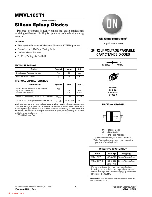
Features
• High Q with Guaranteed Minimum Values at VHF Frequencies • Controlled and Uniform Tuning Ratio • Surface Mount Package • Pb−Free Package is Available
MILLIMETERS
DIM MIN NOM MAX
A 0.80 0.90 1.00
A1 0.00 0.05 0.10
A3
0.15 REF
b 0.25 0.32 0.4
C 0.089 0.12 0.177
D 1.60 1.70 1.80
E 1.15 1.25 1.35
L 0.08
HE 2.30 2.50 2.70
V(BR)R
30
−
−
Vdc
IR
−
−
0.1
mAdc
TCC
−
300
−
ppm/°C
Ct, Diode Capacitance VR = 3.0 Vdc, f = 1.0 MHz
pF
Device
Min
Nom
Max
MMVL109T1
26
29
32
2. CR is the ratio of Ct measured at 3 Vdc divided by Ct measured at 25 Vdc.
DDG2001型电导仪用户手册

2000 Series In line water qualityanalysis apparatus with ChineseinterfaceDDG-2001 Intelligent electric conductivity meterSTATE ELECTRIC POWER CORPARATION, P . R. C.NANJING ELECTRIC POWER AUTOMATION EQUIPMENT GENERAL FACTORYUser ManualSoftware version :DDG V2.0CHAPTER I PREFACE (2)1.1 O PERATING INSTRUCTIONS (2)1.3F UNCTIONAL F EATURES (3)1.4 A PPLICATION RANGE (3)CHAPTER II INSTALLATION & WIRING (4)2.1O PEN BOX (4)2.2O VERALL SIZE (4)2.4W IRING (5)2.5A DJUST DISPLAY CONTRAST GRADIENT (6)2.6E LECTRICITY C ONNECTION FOR MEASURING SYSTEM (6)CHAPTER III ABOUT ELECTRODE (9)CHAPTER ⅣOPERATION (10)4.1B E FAMILIAR WITH FRONT PANEL (10)4.2D ISPLAY SCREEN AND FUNCTION KEY (10)4.3SYMBOL (11)4.4H OW TO CHOOSE MENU ITEM (11)4.5I NPUT AND MODIFICATION OF NUMERICAL V ALUE (11)4.6E XIT FROM MENU (12)CHAPTER ⅤPROGRAMMING INSTRUCTION (12)5.1S WITCH-OVER OF THE DISPLAY INTERFACE (12)5.2M AIN MENU (12)5.3C ALIBRATION M ENU (13)5.4M ENU MAINTENANCE (15)5.5P ROGRAMMING MENU (15)CHAPTER ⅥTEST AND SIMULATION TEST (23)CHAPTER ⅦTECHNICAL SPECIFICATION (25)CHAPTER ⅧRUNNING, MAINTENANCE AND SERVICE (27)APPENDIX A (30)DEFAULT V ALUE (30)Chapter I PrefaceOperating instructionsThanks for your choice of DDG-2001 intelligent electric conductivity meters manufactured by our factory.Please read this book to help you understand and use this product correctly, and hope to have your feedback about product performance and quality from your side. To get your trust is our start point and purpose. We guarantee to provide technical support and service after sales to you. Please read it carefully for you to use this product safely and conveniently.1. This apparatus has been past the strict test before dispatched from factory. Normally noneed to do any adjustment if there is no severe damage after open the box. Please configure parameter according to your requirements.2. The apparatus should be mounted on the instrument cabinet correctly in good fixations.3. The panel of the apparatus is soft touch, please touch it slightly and don’t press keyboard with hard material.4. The display part of the apparatus should not be collide or scuffing.5. As the special requirement of customer and unceasing perfect needs of software as well as the function has increased, the software is always being upgraded and changed. So every software and user manual has the edition number. There is the edition explanation on the cover of the user manual. Please pay attention that the edition of user manual should be identical with that of the software.1.2 Summary of product2001 industrial in line electricity conductive apparatus is one of 2000 series in line water quality analyzer meter, an intelligent continuous monitoring apparatus in line. It can be used in combination with various of the electricity conductive measuring pools produced by our company to meet various kinds of requirements in different applications It is widely used in water supply to boiler in electricity generator, steam condensation water and continuously measure super water electricity conductive ratio.2001 industrial in line electricity conductive apparatus is a multi function device with new concept, integrated electricity conductive measurement, temperature and temperature compensation measurement, alarm controller as well as super calculation. It is applied in various fields.Chinese interface---total Chinese crystal liquid multi parameter displayed simultaneously, menu reminder, simple operating, friendly human-machine interface.Simple operation---simple human-machine interface make user quickly master its operation and running.High intelligent---adopts single chip micro process technology to minimize the size and improve the anti-interference ability and reliability.Running reliability---integrated with multiple anti-interference technology to guarantee the accuracy of measurement and running reliability.Multi function and practical---multiple output to form a good measuring system in line.Communication function---standard light and electricity isolated RS485 interface to be conveniently connected with printer, data trans-recorder and link up the computer networks to form a distributed control system1.3 Functional Features●Adopts international standard and modular design, DIN144×144 international standard shell, 180mm in longwise to minimize the space between the control boxes.●Total Chinese crystal liquid multi parameter display at the same time, menu reminder, simple operation, friendly human-machine. Water proof key board with 4 bits soft touch and function reminder to make the operation very easy without special training.●Liquid crystal screen with heliotropism to guarantee the use in poor light.● Incentive power of electrode is plus-minus equal electrical potential pulse wave with accurate waveform and stable scope under micro process controlling, efficiently eliminate polarization effect and influence from capacity effect.● Realize auto switching in the measuring range that covered by electrode.●Each function and parameter is set by software without function switch and adjusting knob.●Temperature auto compensated within 0-60℃, also can be set as manual operation. User can program temperature coefficient to meet the requirements of different water quality.●Access code is separately set calibration and programming to prevent the operation of non related personnel●Optical isolated 2 circuits analog quantity DC 4-20Ma output, user programming corresponding to pH.Optical isolation 4 circuits relay switch quantity output, user program sets the relay working status.● Optical isolation RS-485 communicating interface, can be linked with the equipment such as printer, data trans-memory etc for recording historical data; also can be net with a group of instruments to form a net, and linked with computer to realize long distance communication for centralized management.● Adopt the technology of WATCHDOG circuit, software pitfall, protection for power off,and digital filtering etc, attach importance to the on-site-fault tolerance capability to make the apparatus be equipped with strong anti-interference ability. Sensor input/microprocessor chip/power/isolation in each output module to restrain various interference of Industrial fields on spot effectively.1.4Application rangeIt is designed to meet the requirements of Industrial usage in wide range, including: super pure water, super water, drinking water and sewage water treatment and inspection. It is applicable in electricity generator, petrochemicals, pharmacy, food and light mechanical industry.Chapter II Installation & Wiring2.1 Open boxInspect accessories and materials of apparatus●main machine 1pc●user manual 1pc●electric conductance flow pool 1pc●measuring electrode for electric conductance 1pc●connecting cable1pc●certification of quality 1pcRemark: 1:RS485 communication interface is an optional accessory, not included in the normal supply range.2:Configure connection cable as standard length of 5 meters.2.2 Overall sizeSee following diagram2.3 Opening the hole installationThis apparatus should be installed on the open base with hole opening size: 138+0.5×138+0.5mm(see following drawing)Installation method: first insert the apparatus into the mounting hole from back side, put two plastic ejector pin to the upper and bottom part of the fixing hole separately, then tighten the screw stem.Requirements for on site installation:there should be no high electricity, strong magnetic field nearby the spot and acid gas. It’s better to fix the apparatus on the best view level during installation, keep the surface clean and dry, prevent it from water splashing and direct sunshine. It should be grounded safely.2.4 WiringSee following wiring scheme and connect it correctly.The terminal in single row on the left of the back of apparatus is input terminal, and the terminal on the right in double row is output terminal.Reminder!Apparatus should be grounded safely to avoid electric shock!!!It’s forbidden to open the out shell of apparatus after it is switched on. Please cut off power to inspection the apparatus. When first installation, switched on the instrument after it was completely connected.Reminder!AC power should be cut off while in wiring!!!2.5 Adjust display contrast gradientIf the contrast gradient of display is found very low and the character displayed dimly after apparatus is switched on, please press confirmation key continuously in the display 1 interface to increase the gradient or press exit key to decrease the gradient. Be caution that this function will be canceled after the apparatus is switched on for 5 minutes.2.6 Electricity Connection for measuring systemCable for connecting electric conductive pool:Cable length:5/10/20m(standard length is 5 meters, special requirement should be noted on purchasing. The maximum length is 30 meters).Typical electricity connection for measuring system:Chapter III About electrodeThere are 2 kinds of electrode that is matched with this apparatus for your choice according to the measuring range, it is a bi-electrode measuring sensor consisted of electric conductive electrode and temperature electrode, connect secondary meter by 5 cores shielding cable with plug.3.1 The structure and size for bi -electrode measuring sensor5 cores cable connector join up in plug-in-mounting, mounting screw thread (standard 3/4"PTX )Overall size :Φ37.5×1183.2 Measure the conductanceChoose the matched electrode according to themeasuring range: Remark 1: As the discreteness in manufacture engineering, every electrode has its own constant that has been marked before dispatching from factory by a label sticking on the electrode with constant written on. Please check the constant before setting the parameter to electrode.Remark 2: the plug of electrode may come loose after used for a long time, that will result in the bad contact. User can clamp the spring leaf. 3.3 Temperature measurementThe temperature measuring unit of electrode is Pt100 platinum electrode. 3.4 Clean and install for electrodeIt suggested to do the first inspection after running for several days, when electrode is newly mounted on the tube system. If there is oil stains, iron rust and sediments etc. on the surface, it should be cleared.Electrode should be done inspection periodically if the measuring system run in a long term and clean electrode when it is found to be polluted. If it is the ooze and particle deposited on the surface of electrode that affect the measuring accuracy, please use soft and clean tower or cotton to wipe them lightly.Various methods to clean: use 5% hydrochloric acid compounded with 3% ablation to clearboiler scale or iron rust;use 5%~10% wash solute to clean oil and fat or oil-bearing by brush. Use cotton ball immersed in organic solvent organosol of absolute ethyl alcohol or carbon tetrachloride to clean the oil-bearing if it is more. Be caution not splash the organic solvent on the plastic screw thread of electrode and out shell. Immerse it for the normal contaminate or heating it a little without exceed the temperature of 40℃.The sleeve of electrode should be screwed slightly without too tighten or too loose when the electrode is repositioned after cleaning. If the electrode is found in big error in measuring system, the constant of electrode should be standardized.Wash clean the electrode for 5 minutes before it is put into use, then soak it in the distilled water that should be change regularly for 15 minutes. All the wash is for the barrel shell of the metal material of electrode and inner damp.Chapter ⅣOperation4.1 Be familiar with front panel4.2 Display screen and function keyThe key has various function according to the prompts on the display screen (reverse display for status)Contrasttablefordisplayscreenandfunctionkey4.3symbolInitialization symbol save symbol4.4 How to choose menu itemThe menu structure is gradation in pull-down type, it ’s easy to select the menu items according to the reminder from screen.For example: menu level in programming the current output 例:电流输出的编程操作的菜单层次4.5 Input and modification of numerical valueUnder the statement of input and modify numerical value, press choose key to change the position of reverse white value, press modification key to change numerical value (0-9 circulation) and press confirmation key to make it become effect.main displayFirst level menusecond level menu4.6 Exit from menuWhen finished the operation for menu, want to exit from menu and return to measuring status, the apparatus provide two methods to return : a. press exit key ( or press this key for many times) to return to the measuring status instantly; b. timeout exit: no need to press key in non maintenance state, apparatus will automatically return to measuring status in 10 minutes later. This function is specially designed for avoiding failure of measuring for a long time due to wrong operation.Chapter ⅤProgramming instruction5.1 Switch-over of the display interfaceThe apparatus provides 3 display interface for your choice by press function key display 1-3 to change the display interface in circulation.5.2 Main menuThe function of main menu is very important as it summarize all the function of the apparatus. Know it in details will bring many conveniences to you for your use.5.3 Calibration MenuThe apparatus needs to be calibrated if big error is found in the periodical inspection before it is put into run, that has great importance for the apparatus to run accurately and reliably.5.3.1 Calibrate the electric conductanceAfter the new purchased apparatus or the electrode whose constant has been calibrated is put into running, it just need setting the calibrating coefficient as 100% and input the correct electrode constant. See chapter 5.3.3 for the setting the electrode constant.The electricity conductance needs to be calibrated if the big error is found. Calibrating the electricity conductance is to adjust the constant error of electricity conductive electrode.To the unknown constant of electrode or the electrode needs to calibrate the electrode constant, set the electrode constant as 0.1 if the matched electrode is 0.1; set it as 0.01 if the matched electrode is 0.01. See chapter 5.3.3 for modifying the electrode constant. The electric conductance ratio of calibration liquid should be close to the ratio.Soak the electrodein the distilled water (electric conductance ration <0.5µS/cm) that changed regularly for 15 minutes before calibrating it and choose the temperature compensation as linearity or unused, then clean electrode for 2-3 times by calibrating liquid. Every time the solution among double layer of inner electrode and outer electrode should be tumble-dry before the electrode is put into the calibration liquid.Remark 1: see the related standards for configure the solution of standard electric conductanceratio.Remark 2: the temperature coefficient of electric conductance ratio is affected by theelectrolyte type and density as well as the temperature of sample water. Although the electric conductance apparatus has the function of auto temperature compensation, it is hard to reach the complete compensation, it is just the approximate. It suggested to choose temperature compensation as unused in calibrating conductance as far as possible. Remark 3: press exit key to go to calibrating menu and recalibrate the parameter if thecalibration parameter exceed the limitation. Check the wiring and electrode of measuring system if the parameter always exceed the limits through many times calibration. Or refer to methods of chapter 6.2 to test the secondary meter.Remark 4: If want to set the calibrate coefficient as 100%, pull up the plug of electrode andsecondary meter and wait till the apparatus indicate as 0.0 µS/cm to go the status of electric conductance calibration, continuously press confirm without put in any value to set the calibration coefficient as 100%.Prompting! The data will be saved and become effective if the save symbol appearsin the middle of the screen after pressing the confirm key.5.3.2 Temperature compensationThe temperature needs to be calibrated due to the discreteness in manufacture engineering of temperature sensor by the water solution with temperature and resistance box.If use resistance box to calibrate need to connect to resistance box by three wire system and replace temperature sensor by resistance box, choose the suitable resistance to calibrate it.Remark: press exit key to go to calibration menu to recalibrate the temperature difference if it exceed the limits. Check the wiring and electrode of measuring system if the parameter always exceed the limits through many times calibration. Or refer to methods of chapter 6.2 to test the secondary meter.Prompting! The data will be saved and become effective if the save symbol appearsin the middle of the screen after pressing the confirm key.Remark: see chapter 6.4 or related standard to standardize the electrode constant.Remark 1: It’s necessary to first confirm the legality of the input data, then save it. Input the the illegal data will bring the results without knowing beforehand.Remark 2: Adopt the method of delay revoke to alarm 1/2/3 to prevent the relay’s contact point nearby the alarm from come into being tremble. The relay will act instantly when the electric conductance reach the alarm value; while the relay will not release at once until the electric conductance fall to a certain value. The same method as the alarming for the temperature exceeding the limits.For example: if the upper limit of alarm is set as 1.25µS/cm, the alarm 1 will act when it reached 1.25µS/cm; while alarm1 relay will not released instantly when the electricconductance fall to 1.25µS/cm till it fall to (1.25-Δ)µS/cm. The normal Δvalue is.05µS/cm。
CM200DY-24H中文资料

Units °C °C Volts Volts Amperes Amperes Amperes Amperes Watts N·m N·m Grams Vrms
Static Electrical Characteristics, Tj = 25 °C unless otherwise specified
COLLECTOR-EMITTER SATURATION VOLTAGE CHARACTERISTICS (TYPICAL)
400
COLLECTOR CURRENT, IC, (AMPERES) COLLECTOR CURRENT, IC, (AMPERES)
400
COLLECTOR-EMITTER SATURATION VOLTAGE, VCE(sat), (VOLTS)
Sep.1998
元器件交易网
MITSUBISHI IGBT MODULES
CM200DY-24H
HIGH POWER SWITCHING USE INSULATED TYPE
OUTPUT CHARACTERISTICS (TYPICAL)
TRANSFER CHARACTERISTICS (TYPICAL)
7 5 3 2
Tj = 25°C
102
Cies
8
IC = 400A
101
Coes
6
FREE-WHEEL DIODE FORWARD CHARACTERISTICS (TYPICAL)
CAPACITANCE VS. VCE (TYPICAL)
10
COLLECTOR-EMITTER SATURATION VOLTAGE, VCE(sat), (VOLTS)
103
IRMCK311TR;中文规格书,Datasheet资料
Data Sheet No. PD60338IRMCK311 Dual Channel Sensorless Motor Control IC forAppliancesFeaturesMCE TM (Motion Control Engine) - Hardware based computation engine for high efficiency sinusoidal sensorless control of permanent magnet AC motor Integrated Power Factor Correction controlSupports both interior and surface permanent magnet motorsBuilt-in hardware peripheral for single shunt current feedback reconstructionNo external current or voltage sensing operational amplifier requiredDual channel three/two-phase Space Vector PWM Three-channel analog output (PWM)Embedded 8-bit high speed microcontroller (8051) for flexible I/O and man-machine controlJTAG programming port for emulation/debugger Two serial communication interface (UART)I2C/SPI serial interfaceWatchdog timer with independent analog clockThree general purpose timers/countersTwo special timers: periodic timer, capture timer Internal ‘One-Time Programmable’ (OTP) memory and internal RAM for final production usagePin compatible with IRMCF311 RAM version1.8V/3.3V CMOS Product SummaryMaximum crystal frequency 60 MHz Maximum internal clock (SYSCLK) frequency 128 MHz Maximum 8051 clock frequency 33 MHz Sensorless control computation time 11 μsec typ MCE TM computation data range 16 bit signed 8051 OTP Program memory 56K bytes MCE program and Data RAM 8K bytes GateKill latency (digital filtered) 2 μsec PWM carrier frequency counter 16 bits/ SYSCLK A/D input channels 6 A/D converter resolution 12 bits A/D converter conversion speed 2 μsec 8051 instruction execution speed 2 SYSCLK Analog output (PWM) resolution 8 bits UART baud rate (typ) 57.6K bps Number of I/O (max) 14 Package (lead-free) QFP64 Operating temperature -40°C ~ 85°CDescriptionIRMCK311 is a high performance OTP based motion control IC designed primarily for appliance applications. IRMCK311 is designed to achieve low cost and high performance control solutions for advanced inverterized appliance motor control. IRMCK311 contains two computation engines. One is Motion Control Engine (MCE TM) for sensorless control of permanent magnet motors; the other is an 8-bit high-speed microcontroller (8051). Both computation engines are integrated into one monolithic chip. The MCE TM contains a collection of control elements such as Proportional plus Integral, Vector rotator, Angle estimator, Multiply/Divide, Low loss SVPWM, Single Shunt IFB. The user can program a motion control algorithm by connecting these control elements using a graphic compiler. Key components of the sensorless control algorithms, such as the Angle Estimator, are provided as complete pre-defined control blocks implemented in hardware. A unique analog/digital circuit and algorithm to fully support single shunt current reconstruction is also provided. The 8051 microcontroller performs 2-cycle instruction execution (16MIPS at 33MHz). The MCE and 8051 microcontroller are connected via dual port RAM to process signal monitoring and command input. An advanced graphic compiler for the MCE TM is seamlessly integrated into the MATLAB/Simulink environment, while third party JTAG based emulator tools are supported for 8051 developments. IRMCK311 comes with a small QFP64 pin lead-free package.TABLE OF CONTENTS1 Overview (5)2 IRMCK311 Block Diagram and Main Functions (6)3 Pinout (8)4 Input/Output of IRMCK311 (9)4.1 8051 Peripheral Interface Group (10)4.2 Motion Peripheral Interface Group (10)4.3 Analog Interface Group (11)4.4 Power Interface Group (11)4.5 Test Interface (12)5 Application Connections (13)6 DC Characteristics (14)6.1 Absolute Maximum Ratings (14)6.2 System Clock Frequency and Power Consumption (14)6.3 Digital I/O DC Characteristics (15)6.4 PLL and Oscillator DC Characteristics (15)6.5 Analog I/O DC Characteristics (16)6.6 Under Voltage Lockout DC Characteristics (17)6.7 AREF Characteristics (17)7 AC Characteristics (18)7.1 PLL AC Characteristics (18)7.2 Analog to Digital Converter AC Characteristics (19)7.3 Op Amp AC Characteristics (19)7.4 SYNC to SVPWM and A/D Conversion AC Timing (20)7.5 GATEKILL to SVPWM AC Timing (21)7.6 Interrupt AC Timing (21)7.7 I2C AC Timing (22)7.8 SPI AC Timing (23)7.8.1 SPI Write AC timing (23)7.8.2 SPI Read AC Timing (24)7.9 UART AC Timing (25)7.10 CAPTURE Input AC Timing (26)7.11 JTAG AC Timing (27)7.12 OTP Programming Timing (28)8 I/O Structure (29)9 Pin List (32)Dimensions (35)10 Package11 Part Marking Information (36)Information (36)12 OrderingTABLE OF FIGURESFigure 1. Typical Application Block Diagram Using IRMCK311 (5)Figure 2. IRMCK311 Internal Block Diagram (6)Figure 3. IRMCK311 Pin Configuration (8)Figure 4. Input/Output of IRMCK311 (9)Figure 5. Application Connection of IRMCK311 (13)Figure 6. Clock Frequency vs. Power Consumption (14)Figure 7 Crystal oscillator circuit (18)Figure 8 Voltage droop of sample and hold (19)Figure 9 SYNC to SVPWM and A/D conversion AC Timing (20)Figure 10 GATEKILL to SVPWM AC Timing (21)Figure 11 Interrupt AC Timing (21)Figure 12 I2C AC Timing (22)Figure 13 SPI AC Timing (23)Figure 14 SPI Read AC Timing (24)Figure 15 UART AC Timing (25)Figure 16 CAPTURE Input AC Timing (26)Figure 17 JTAG AC Timing (27)Figure 18 OTP Programming Timing (28)Figure 19 All digital I/O except motor PWM output (29)Figure 20 RESET, GATEKILL I/O (29)Figure 21 Analog input (30)Figure 22 Analog operational amplifier output and AREF I/O structure (30)Figure 23 VPP programming pin I/O structure (30)Figure 24 VSS and AVSS pin structure (31)Figure 25 VDD1 and VDDCAP pin structure (31)Figure 26 XTAL0/XTAL1 pins structure (31)TABLE OF TABLESTable 1. Absolute Maximum Ratings (14)Table 2. System Clock Frequency (14)Table 3. Digital I/O DC Characteristics (15)Table 4. PLL DC Characteristics (15)Table 5. Analog I/O DC Characteristics (16)Table 6. UVcc DC Characteristics (17)Table 7. AREF DC Characteristics (17)Table 8. PLL AC Characteristics (18)Table 9. A/D Converter AC Characteristics (19)Table 10. Current Sensing OP Amp AC Characteristics (19)Table 11. SYNC AC Characteristics (20)Table 12. GATEKILL to SVPWM AC Timing (21)Table 13. Interrupt AC Timing (21)Table 14. I2C AC Timing (22)Table 15. SPI Write AC Timing (23)Table 16. SPI Read AC Timing (24)Table 17. UART AC Timing (25)Table 18. CAPTURE AC Timing (26)Table 19. JTAG AC Timing (27)Table 20. OTP Programming Timing (28)Table 21. Pin List (32)1 OverviewIRMCK311 is a new International Rectifier integrated circuit device primarily designed as a one-chip solution for complete inverter controlled appliance dual motor control applications. Unlike a traditional microcontroller or DSP, the IRMCK311 provides a built-in closed loop sensorless control algorithm using the unique Motion Control Engine (MCE TM) for permanent magnet motors. The MCE TM consists of a collection of control elements, motion peripherals, a dedicated motion control sequencer and dual port RAM to map internal signal nodes. IRMCK311 also employs a unique single shunt current reconstruction circuit to eliminate additional analog/digital circuitry and enables a direct shunt resistor interface to the IC. The sensorless control is the same for both motors with a single shunt current sensing capability. Motion control programming is achieved using a dedicated graphical compiler integrated into the MATLAB/Simulink TM development environment. Sequencing, user interface, host communication, and upper layer control tasks can be implemented in the 8051 high-speed 8-bit microcontroller. The 8051 microcontroller is equipped with a JTAG port to facilitate emulation and debugging tools. Figure 1 shows a typical application schematic using IRMCK311.IRMCK311 is intended for volume production purpose and contains 64K bytes of OTP (One Time Programming) ROM, which can be programmed through a JTAG port. For a development purpose use, IRMCF311 contains a 48k byte of RAM in place of program OTP to facilitate an application development work. Both IRMCF311 and IRMCK311 come in the same 64-pin QFP package with identical pin configuration to facilitate PC board layout and transition to mass productionFigure 1. Typical Application Block Diagram Using IRMCK3112 IRMCK311 Block Diagram and Main FunctionsM o t i o n C o n t r o l B u sFigure 2. IRMCK311 Internal Block DiagramIRMCK311 contains the following functions for sensorless AC motor control applications:• Motion Control Engine (MCE TM )o Proportional plus Integral block o Low pass filtero Differentiator and lag (high pass filter) o Ramp o Limito Angle estimate (sensorless control) o Inverse Clark transformation o Vector rotator o Bit latch o Peak detect o Transitiono Multiply-divide (signed and unsigned)o Divide (signed and unsigned)o Addero Subtractoro Comparatoro Countero Accumulatoro Switcho Shifto ATAN (arc tangent)o Function block (any curve fitting, nonlinear function)o16-bit wide Logic operations (AND, OR, XOR, NOT, NEGATE)o MCE TM program and data memory (6K byte). Note 1o MCE TM control sequencer• 8051 microcontrollero Three 16-bit timer/counterso16-bit periodic timero16-bit analog watchdog timero16-bit capture timero Up to 36 discrete I/Oso Eleven-channel 12-bit A/DFive buffered channels (0 – 1.2V input)One unbuffered channel (0 – 1.2V input)o JTAG port (4 pins)o Up to three channels of analog output (8-bit PWM)o Two UARTo I2C/SPI porto 64K byte Note 1program One-Time Programmable memoryo2K byte data RAM. Note 2Note 1: Total size of OTP memory is 64K byte, however MCE program occupiesmaximum 8K byte which will be loaded into internal RAM at a powerup/bootprocess. Therefore only 56K byte OTP memory area is usable for 8051microcontroller.Note 2: Total size of RAM is 8K byte including MCE program, MCE data, and 8051data. Different sizes can be allocated depending on applications.3 PinoutXTAL0XTAL1P1.1/RXD P1.2/TXDVDD1VSS VDD2P1.3/SYNC/SCKP1.4/CAPP 3.6/R X D 1P 3.7/T X D 1FPWMVL FPWMUL V S SV D D 2A V D DA V S SA I N 0A R E FP 2.7/A O P W M 1P 2.6/A O P W M 0CPWMUH CPWMVH CPWMWH CPWMUL CPWMVL CPWMWL CGATEKILL VDD1VSS I F B C OI F B C +I F B C -P L L V S SP L L V D DR E S E TN CT C KP 5.3/T D IP 5.2/T D OP 5.1/T M SS D A /C S 0S C L /S O -S I /V P PP 5.0/P F C G K I L LP F C P W M V S SFGATEKILL FPWMWL VAC-VAC+VACO IPFCO IPFC+IPFC-I F B F OI F B F +I F B F -P3.0/INT2/CS1C M E X TFPWMVH FPWMUHFPWMWH A I N 1P 3.2/I N T 0Figure 3. IRMCK311 Pin Configuration4 Input/Output of IRMCK311All I/O signals of IRMCK311 are shown in Figure 4. All I/O pins are 3.3V logic interface except A/D interface pins.Figure 4. Input/Output of IRMCK3114.1 8051 Peripheral Interface GroupUART InterfaceP1.1/RXD Input, Receive data to IRMCK311, can be configured as P1.1P1.2/TXD Output, Transmit data from IRMCK311, can be configured as P1.22nd channel Receive data to IRMCK311, can be configured as P3.6 P3.6/RXD1 Input,P3.7/TXD1 Output,2nd channel Transmit data from IRMCK311, can be configured as P3.7Discrete I/O InterfaceP1.3/SYNC/SCK Input/output port 1.3, can be configured as SYNC output or SPI clock P1.4/CAP Input/output port 1.4, can be configured as Capture Timer inputP3.0/INT2/CS1 Input/output port 3.0, can be configured as external interrupt 2 or SPIchip select 1P3.2/INT0 Input/output port 3.2, can be configured as external interrupt 0Analog Output InterfaceP2.6/AOPWM0 Input/output, can be configured as 8-bit PWM output 0 withprogrammable carrier frequencyP2.7/AOPWM1 Input/output, can be configured as 8-bit PWM output 1 withprogrammable carrier frequencyCrystal InterfaceXTAL0 Input, connected to crystalXTAL1 Output, connected to crystalReset InterfaceRESET Inout, system reset, needs to be pulled up to VDD1 but doesn’t requireexternal RC time constantI2C/SPI InterfaceSCL/SO-SI/VPP Output, I2C clock output, SPI SO-SII2C Data line, Chip Select 0 of SPISDA/CS0 Input/output,P3.0/INT2/CS1 Input/output port 3.0, can be configured as external interrupt 2 or SPIchip select 1P1.3/SYNC/SCK Input/output port 1.3, can be configured as SYNC output or SPI clock 4.2 Motion Peripheral Interface GroupPWMCPWMUH Output, motor 1 PWM phase U high side gate signalCPWMUL Output, motor 1 PWM phase U low side gate signalCPWMVH Output, motor 1 PWM phase V high side gate signalCPWMVL Output, motor 1 PWM phase V low side gate signalCPWMWH Output, motor 1 PWM phase W high side gate signalCPWMWL Output, motor 1 PWM phase W low side gate signalFPWMUH Output, motor 2 PWM phase U high side gate signalFPWMUL Output, motor 2 PWM phase U low side gate signal分销商库存信息: IRIRMCK311TR。
索尼KV-DA34M80
C083 XX IC2600 PQ09RD21 9V REG
L013 10UH C018 0.22 16V B CHIP R025 100 CHIP
VDDC4(1.8) L010 10uh 125 VDDA3(3.3V) L033 10uh 124 VREF_POS_LSL 123VREF_NEG_LSL+LSR 122 VREF_POS_LSR+HPL C031 470 16V 121 VREF_NEG_HPL+HPR 120 VREF_POS_HPR C032 XX 119 XTALIN 118 XTALOUT C034 XX C086 0.1 B 117 VSSA1 116 VGUARD 115 DECDIG 114 VP1 113 PH2LF R044 12k 112 PH1LF 111 GND1 C048 0.22 16V B 110 SECPLL 109 DECBG R045 100 CHIP 108 EWD R046 100 CHIP 107 VD106 VD+ 105 VIFIN2 104 VIFIN1 103 VSC 102 IREF 101 GNDIF 100 SIFIN1 99 SIFIN2 C057 0.01 25V B CHIP 98 AGCOUT 97 EHTO
+9V 001:16J;002:8L; 003:15A D
R336 10k CHIP
D002 MMDL914T1 3.3V SUPPLY R001 4.7k CHIP R010 10k CHIP D003 MMDL914T1 5V SUPPLY
R395 4.7k CHIP
C023 0.22 C096 16V XX B CHIP C097 XX
R2611 10K CHIP
DW01中文资料

一、主要特性静态电流待机电流(检测到过放之后)过充检测精度(Topt=25℃)过充检测精度(Topt=0 到50℃)过放检测精度过放检测电压过流保护过充延迟(VDD=4.4V)过放延迟(VDD=2.2V 带有内置电容)封装典型值:4.0uA典型值:0.2uA±50mV±60mV±100mV2.0V 到3.0V,每步0.005V 0.04V 到0.32V,每步0.04V 110mS22mS(最小值)SOT23-6/6-pin二、基本描述DW01 是一款单节可充电锂电池保护集成电路,具有过充、过放、过流及短路保护功能。
IC 内部包含:三个电压检测电路、一个基准电路、一个延迟电路、一个短路保护电路和一个逻辑电路。
当充电电压逐渐增大超过过充检测电路的阈值VDET1 时,Cout Pin 的输出电压即过充检测电路的输出电压VD1 会变到低电位,也就是充电器负端的电位。
在进入过充保护状态后,当VDD 电压降低到VREL1 下方或者当电池组脱离充电器而接一个负载,且VDD 介于VDET1 与VREL1 之间时VD1 可以复位,即Cout Pin 输出变为高电位。
当放电电压低于过放检测电路的阈值VDET2 时,经过一段固定的延迟时间,Dout Pin 的输出即过放检测电路的输出VD2 会变为低电位。
这时,若给电池充电,当电池电压上升到过放检测电路的阈值电压之上时,VD2 恢复,Dout 的输出电压变为高电平。
当有过流情况出现时,内部过流检测电路会检测到,经过一段固定的延迟时间后,VD3 和Dout 变为低电平,放电回路被切断。
这时,若将电池组从负载系统中分开,VD3 会恢复使Dout 变为高电平。
当有外部短路电流时,短路保护电路会立即使Dout变为低电位,当外部短路电流消失后,Dout 会转换为高电位。
在检测到过放之后,会通过关闭一些内部电路使电源电流非常低。
IC 过充检测电路的延迟时间可以通过连接外部电容进行设置。
ILD1中文资料

FEATURES•Current Transfer Ratio at I F =10 mA ILD/Q1, 20% Min.ILD/Q2, 100% Min.ILD/Q5, 50% Min.•High Collector-Emitter Voltage ILD/Q1: BV CEO =50 VILD/Q2, ILD/Q5: BV CEO =70 V•Field-Effect Stable by TRansparent IOn Shield (TRIOS) Isolation Test Voltage, 5300 VAC RMS• Underwriters Lab File #E52744• VDE 0884 Available with Option 1Maximum Ratings (Each Channel)EmitterReverse Voltage ................................................6 V Forward Current ...........................................60 mA Surge Current................................................. 2.5 A Power Dissipation.......................................100 mW Derate Linearly from 25 ° C..................... 1.3 mW/ ° C DetectorCollector-Emitter Reverse VoltageILD/Q1........................................................... 50 V ILD/Q2, ILD/Q5...............................................70 V Collector Current.......................................... 50 mA Collector Current (t<1 ms)...........................400 mA Power Dissipation.......................................200 mW Derate Linearly from 25 ° C......................2.6 mW/ ° C PackageIsolation Test Voltage (between emitter and detector referred to standard climate 23 ° C/50%RH,DIN 50014)....................................5300 VAC RMS Creepage...............................................min. 7 mm Clearance...............................................min. 7 mm Isolation ResistanceV IO =500 V , T A =25 ° C .........................R IO =10 12 Ω V IO =500 V , T A =100 ° C .......................R IO =10 11 Ω Package Power Dissipation ...................... 250 mW Derate Linearly from 25 ° C..................... 3.3 mW/ ° C Storage Temperature................... –40 ° C to +150 ° C Operating Temperature................–40 ° C to +100 ° C Junction Temperature....................................100 ° C Soldering Temperature(2 mm from case bottom)..........................260 ° CV D E DESCRIPTIONThe ILD/Q1/2/5 are optically coupled isolated pairs employing GaAs infrared LEDs and silicon NPN phototransistor. Signal information, including a DC level, can be transmitted by the drive while maintaining a high degree of electrical isolation between input and output. The ILD/Q1/2/5 are especially designed for driving medium-speed logic and can be used to eliminate trou-blesome ground loop and noise problems. Also these couplers can be used to replace relays and transformers in many digital interface applica-tions such as CRT modulation. The ILD1/2/5 has two isolated channels in a single DIP package and the ILQ1/2/5 has four isolated channels per pack-age.See Appnote 45, “How to Use Optocoupler Normalized Curves.”Dimensions in inches (mm).268 (6.81).255 (6.48).790 (20.07).779 (19.77 ).045 (1.14).030 (.76).100 (2.54) Typ.3°–9°.305 Typ. (7.75) Typ..022 (.56).018 (.46).012 (.30).008 (.20).135 (3.43).115 (2.92)Pin One I.D.Pin One I.D..150 (3.81).130 (3.30).040 (1.02).030 (.76 ).268 (6.81).255 (6.48)3465.390 (9.91).379 (9.63).045 (1.14).030 (.76)4° Typ.4° Typ..100 (2.54) Typ.10° Typ.10° Typ.3°–9°.305 Typ.(7.75) Typ..022 (.56).018 (.46).012 (.30).008 (.20).135 (3.43).115 (2.92)1287.150 (3.81).130 (3.30).040 (1.02).030 (.76 )12348765Emitter Collector Collector EmitterAnode Cathode Cathode Anode 16151413121110 912345678Emitter Collector Collector Emitter Emitter Collector Collector EmitterAnode Cathode Cathode Anode Anode Cathode Cathode Anode Quad ChannelDual ChannelDUAL CHANNEL ILD1/2/5 QUAD CHANNEL ILQ1/2/5PHOTOTRANSISTOROPTOCOUPLER元器件交易网元器件交易网CharacteristicsSymbol Min.Typ.Max.Unit ConditionEmitterForward Voltage V F 1.25 1.65V I F=60 mAReverse Current I R0.0110µA V R=6 VCapacitance C025pF V R=0 V, f=1 MHzThermal Resistance, Junction to Lead R THJL750°C/WDetectorCapacitance C CE 6.8pF V CE=5 V, f=1 MHzLeakage Current, Collector-Emitter I CEO550nA V CE=10 VSaturation Voltage, Collector-Emitter V CESAT0.250.4I CE=1 mA, I B=20 µADC Forward Current Gain HFE2006501800V CE= 10 V, I B=20 µASaturated DC Forward Current Gain HFE SAT120400600V CE= 0.4 V, I B=20 µAThermal Resistance, Junction to Lead R THJL500°C/WPackage Transfer Characteristics (Each Channel)Symbol Min.Typ.Max.Unit Condition ILD/Q1Saturated Current Transfer Ratio (Collector-Emitter)CTR CESAT75%I F=10 mA, V CE=0.4 VCurrent Transfer Ratio (Collector-Emitter)CTR CE2090300%I F=10 mA, V CE=10 VILD/Q2Saturated Current Transfer Ratio (Collector-Emitter)CTR CESAT170%I F=10 mA, V CE=0.4 VCurrent Transfer Ratio (Collector-Emitter)CTR CE100200500%I F=10 mA, V CE=10 VILD/Q5Saturated Current Transfer Ratio (Collector-Emitter)CTR CESAT100%I F=10 mA, V CE=0.4 VCurrent Transfer Ratio (Collector-Emitter)CTR CE50130400%I F=10 mA, V CE =10 VIsolation and InsulationCommon Mode Rejection, Output High C MH5000V/µs V CM=50 V P-P, R L=1 kΩ, I F=0 mA Common Mode Rejection, Output Low C ML5000V/µs V CM=50 V P-P, R L=1 kΩ, I F=10 mA Common Mode Coupling Capacitance C CM0.01pFPackage Capacitance C IO0.8pF V IO=0 V, f=1 MHzTypical Switching TimesFigure 1. Non-saturated switching timingFigure 2. Non-saturated switching timingFigure 3. Saturated switching timingFigure 4. Saturated switching timingV O V CC =5 VR L =75 ΩF=10 KHz,DF=50%I F =10 mA I FV Ot Dt R50%PHL t PLHt St Ft V OV CC =5 V R L F=10 KHz,DF=50%I F =10 mAI FV Ot Dt RV TH =1.5 Vt PHLt PLHt St FFigure 5. Normalized non-saturated and saturated CTR at T A =25 ° C versus LED currentFigure 6. Normalized non-saturated and saturated CTR at T A =25 ° C versus LED currentCharacteristic ILD/Q1I F =20 mA ILD/Q2I F =5 mA ILD/Q5I F =10 mA Unit ConditionDelay, t D 0.8 1.7 1.7 µ s V CE =5 V R L =75 k Ω 50% of V PPRise time, t R 1.9 2.6 2.6 µ s Storage, t S 0.20.40.4 µ s Fall Time, t F1.42.2 2.2 µ s Propagation H-L, t PHL 0.7 1.2 1.1 µs Propagation L-H, t PLH1.42.32.5µsCharacteristicILD/Q1I F =20 mA ILD/Q2I F =5 mA ILD/Q5I F =10 mA Unit ConditionDelay, t D 0.81 1.7µs V CE =0.4 V R L =1 k ΩV CC =5 V V TH =1.5 VRise time, t R 1.227µs Storage, t S 7.4 5.4 4.6µs Fall Time, t F7.613.520µs Propagation H-L, t PHL 1.6 5.4 2.6µs Propagation L-H, t PLH8.67.47.2µs.11101000.70.80.91.01.11.21.31.4If - Forward Current - mAV f -F o r w a r d V o l t a g e - VTa = -55°CTa = 25°CTa = 100°C.11101000.00.51.01.5NCTR(SAT)NCTRIF - LED Current - mAC T R N F - N o r m a l i z e d C T R F a c t o rNormalized to:Vce = 10V, IF = 10mA Ta = 25°CCTRce(sat) Vce = 0.4V元器件交易网Figure 10. Collector-emitter current versus tempera-ture and LED currentFigure 11. Collector-emitter leakage current versus temperatureFigure 12. Propagation delay versus collector load resistor60504030201000510152025303550°C70°C85°CIF - LED Current - mAI c e - C o l l e c t o r C u r r e n t - m A25°C10080604020-2010-210-1100101102103104105Ta - Ambient Temperature - °CI c e o - C o l l e c t o r -E m i t t e r - n ATYPICALVce = 10V .11101001101001000 1.01.52.02.5RL - Collector Load Resistor - K Ωt P L H - P r o p a g a t i o n L o w -H i g h - µst P H L - P r o p a g a t i o n H i g h -L o w - µstPLHtPHLTa = 25°C, IF = 10mA Vcc = 5V, Vth = 1.5V Figure 7. Normalized non-saturated and saturated CTR at T A =50°C versus LED currentFigure 8. Normalized non-saturated and saturated CTR at T A =70°C versus LED currentFigure 9. Normalized non-saturated and saturated CTR at T A =85°C versus LED current.11101000.00.51.01.5NCTR(SAT)NCTRIF - LED Current - mAC T R N F - N o r m a l i z e d C T R F a c t o rNormalized to:Vce = 10V, IF = 10mA, Ta = 25°C Ta = 50°CCTRce(sat) Vce = 0.4V.11101000.00.51.01.5NCTR(SAT)NCTRIF - LED Current - mAC T R - N o r m a l i z e d C T R F a c t o rNormalized to:Vce = 10V, IF = 10mA Ta = 25°CTa = 70°CCTRce(sat) Vce = 0.4V100101.10.00.51.01.5NCTR(SAT)NCTRNormalized to:Vce = 10V, IF = 10mA, Ta = 25°C Ta = 85°C CTRce(sat) Vce = 0.4VIF - LED Current - mAN C T R - N o r m a l i z e d C T R元器件交易网。
D200I资料
Key Features:• 2W Output Power • Miniature SIP Case • Single & Dual Outputs • 3,000 VDC Isolation • >1.12 MHour MTBF • 28 Standard Models •Industry Standard Pin-OutD200IHigh Isolation Miniature, 2W SIP DC/DC Con v ert ersSeriesMicroPower Direct292 Page Street Suite DStoughton, MA 02072USAT: (781) 344-8226F: (781) 344-8481E: sales@ W: RoHS CompliantElectrical Specifi cationsSpecifi cations typical @ +25°C, nominal input voltage & rated output current, unless otherwise noted. Specifi cations subject to change without notice.InputParameterConditions Min.Typ.Max.UnitsInput Voltage Range5 VDC Input 4.55.0 5.5VDC12 VDC Input 10.812.013.224 VDC Input 21.624.026.448 VDC Input 43.248.052.8Input Filter Internal CapacitorRefl ected Ripple Current12 μH Source Inductance 20mA P - POutputParameterConditionsMin.Typ.Max.Units Output Voltage Accuracy ±3.0%Output Voltage Balance Dual Output , Balanced Loads ±1.0%Line Regulation For Vin Change of 1%±1.2%Load RegulationSee Model Selection GuideRipple & Noise (20 MHz)75mV P - P Output Power Protection 120%Temperature Coeffi cient ±0.02%/ºCOutput Short CircuitMomentary (0.5 Sec.)GeneralParameterConditionsMin.Typ.Max.Units Isolation Voltage 60 Seconds 3,000VDC Isolation Resistance 500 VDC 1,000M ΩIsolation Capacitance 100 kHz, 1V60pF Switching Frequency80kHz EnvironmentalParameterConditionsMin.Typ.Max.Units Operating Temperature Range Ambient-40+25+85ºC Operating Temperature Range Case+100ºC Storage Temperature Range -40+125ºC Cooling Free Air ConvectionHumidityRH, Non-condensing95%PhysicalCase Size (5V, 12V & 24V Input Models)0.76 x 0.24 x 0.39 Inches (19.5 x 6.0 x 10.0 mm)Case Size (48V Input Models)0.76 x 0.28 x 0.39 Inches (19.5 x 7.2 x 10.0 mm)Case Material Non-Conductive Black Plastic (UL94-V0)Weight0.08 Oz (2.3g)Reliability Specifi cationsParameter ConditionsMin.Typ.Max.Units MTBFMIL HDBK 217F , 25ºC, Gnd Benign1.12MHours Absolute Maximum RatingsParameterConditionsMin.Typ.Max.UnitsInput Voltage Surge (1 Sec) 5 VDC Input -0.77.0VDC12 VDC Input -0.715.024 VDC Input -0.728.048 VDC Input-0.754.0Lead Temperature1.5 mm From Case For 10 Sec260ºC Internal Power Dissipation All Models650mWCaution: Exceeding Absolute Maximum Ratings may damage the module. These are not continuous operating ratings.Derating Curve• All dimensions are typical in inches (mm) Tolerance x.xx = ±0.01 (±0.25)Pin 1 is marked by a “dot” or indentation on the side of the unit Notes:1. Output load regulation is specifi ed for a load change of 20% to 100%.2. T hese units do not require external components to operate, but the use of an input ca-pacitor (10 μF) may enhance performance in some applications. It is recommended that an input capacitor of 4.7 u F to 47 u F (dependent upon the application) be used on 48V input model.An output capacitor (4.7 μF to 220 μF or ±4.7 μF to ±100 μF) may be used to reduce ripple. To improve EMI performance, a simple fi lter network consisting of a 10 u F to 100 u F capaci-tor and 12 u H inductor should be effective.3. These units will operate at no load without damage, but may not meet all specifi cations.4. D ual output units may be connected to provide a 10V, 24V or 30 VDC output. To do this, connect the load across the positive (+Vout) and negative (-Vout) outputs and fl oat the output common.5. It is recommended that a fuse be used on the input of a power supply for protection. See the table above for the correct rating.Other input/output combinations are available (i.e. 24.0 VDC). Contact the factory for details at:sales@Model Selection GuideMechanical DimensionsPin ConnectionsSingle Output (μF Max)Dual Output (μF Max)470±220Capacitive LoadModel Number InputOutput LoadRegulation (%, Max) Effi ciency(%, Typ)Fuse Rating Slow-Blow (mA)Voltage (VDC)Current (mA)Voltage (VDC)Current (mA, Max)Current(mA, Min)Nominal RangeFull-Load No-Load D201I 5 4.5 - 5.536730 3.3400.010.020721,000D202I 5 4.5 - 5.551230 5.0400.08.010781,000D203I 5 4.5 - 5.55003012.0165.0 3.510821,000D204I 5 4.5 - 5.55003015.0133.0 2.710821,000D205I 5 4.5 - 5.555530±5.0±200.0±4.010721,000D206I 5 4.5 - 5.551230±12.0±83.3±1.710781,000D207I 5 4.5 - 5.550030±15.0±66.6±1.410801,000D211I 1210.8 - 13.216920 3.3400.010.02065500D212I 1210.8 - 13.221620 5.0400.08.01077500D213I 1210.8 - 13.22032012.0165.0 3.51082500D214I 1210.8 - 13.22032015.0133.0 2.71082500D215I 1210.8 - 13.222220±5.0±200.0±4.01075500D216I 1210.8 - 13.220320±12.0±83.3±1.71082500D217I 1210.8 - 13.220320±15.0±66.6±1.41082500D221I 2421.6 - 26.47610 3.3400.010.02072200D222I 2421.6 - 26.410510 5.0400.08.01079200D223I 2421.6 - 26.41021012.0165.0 3.51080200D224I 2421.6 - 26.41011015.0133.0 2.71082200D225I 2421.6 - 26.411110±5.0±200.0±4.01075200D226I 2421.6 - 26.410110±12.0±83.3±1.71082200D227I 2421.6 - 26.410110±15.0±66.6±1.41082200D231I 4843.2 - 52.8456 3.3400.010.02060100D232I 4843.2 - 52.8546 5.0400.08.01077100D233I 4843.2 - 52.853612.0165.0 3.51078100D234I 4843.2 - 52.853615.0133.0 2.71078100D235I 4843.2 - 52.8576±5.0±200.0±4.01073100D236I 4843.2 - 52.8526±12.0±83.3±1.71080100D237I4843.2 - 52.8526±15.0±66.6±1.41080100Pin Single Dual 1+Vin +Vin 2-Vin -Vin 5-Vout -Vout 6No Pin Common 7+Vout+VoutNotes:All dimensio •Tolerance x •Pin 1 is maron the sideMicroPower Direct292 Page Street Ste D Stoughton, MA 02072 • TEL: (781) 344-8226 • FAX: (781) 344-8481 • E-Mail: sales@。
MMBT3904DW1T1G开关三极管规格书

The MMBT3904DW1T1G device is a spin–off of our popular MMBT3904DW1T1GDual General Purpose TransistorsSOT–23/SOT–323 three–leaded device. It is designed for general purpose amplifier applications and is housed in the SOT–363six–leaded surface mount package. By putting two discrete devices in one package , this device is ideal for low–power surface mount applications where board space is at a premium.●FEATURES1)Low VCE(sat), ≤ 0.4 V 2)Simplifies Circuit Design3)Reduces Board Space4)Reduces Component Count5)Available in 8 mm, 7–inch/3,000 Unit Tape and Reel 6)hFE, 100–3007)We declare that the material of product compliant with RoHS requirements and Halogen Free.8) S- Prefix for Automotive and Other Applications Requiring Unique Site and Control Change Requirements; AEC-Q101 Qualified and PPAP Capable.1. Device mounted on FR4 glass epoxy printed circuit board using the minimum recommended footprint.MMBT3904DW1T1G●ELECTRICAL CHARACTERISTICS (Ta= 25℃)2. Pulse Test: Pulse Width <300 μs, Duty Cycle <2.0%.●ELECTRICAL CHARACTERISTICS (Ta= 25℃)(CONTINUED)Figure 1. Delay and Rise TimeEquivalent Test Circuit Figure 2. Storage and Fall TimeEquivalent Test Circuit-ā0010 < t 1 < 500 m * T otal shunt capacitance of test jig and connectorsMMBT3904DW1T1GELRCTRICAL CHARACTERISTICS CURVESFIG.3 Capacitance FIG.4 Current GainFIG.6 Collector Saturation RegionFIG.5 DC Current GainMMBT3904DW1T1G ELRCTRICAL CHARACTERISTICS CURVESFIG.9 VBE(on) vs. ICFIG.7 VCE(sat) vs. IC FIG.8 VBE(sat) vs. IC0.20.40.60.811.21.40.00010.0010.010.11V B E s a t , B a s e -E m i t t e r S a t u r a t i o n V o l t a g e (V )IC, Collector Current(A) 25℃150℃-55℃MMBT3904DW1T1GSC-88NOTES:1. DIMENSIONING AND TOLERANCING PER ANSI Y14.5M, 1982.2. CONTROLLING DIMENSION: INCH.INCHES MILLIMETERSDIMMIN MAXMIN MAX A 0.0710.087 1.80 2.20B 0.0450.053 1.15 1.35C 0.0310.0430.80 1.10D 0.0040.0120.100.30G 0.026 BSC 0.65 BSC H ---0.004---0.10J 0.0040.0100.100.25K 0.0040.0120.100.30N 0.008 REF 0.20 REF S 0.0790.0872.00 2.20PIN 1. EMITTER 22. BASE 23. COLLECTOR 14.EMITTER 15. BASE 16.COLLECTOR 2MMBT3904DW1T1G。
E01-ML01D产品使用手册
nRF24L01P 无线模块E01系列本说明书可能会随着产品的不断改进有所更改,请以最新版的说明书为准成都亿佰特电子科技XX保留对本说明中所有内容的最终解释权与修改权产品概述E01系列是成都亿佰特公司标志性产品的 2.4G 无线模块, SPI 接口,目前已经稳定量产,并适用于多种应用场景。
E01系列采用挪威 Nordic 公司原装进口的 nRF24L01P 芯片,所有阻容感器件均采用进口元器件,尤其是晶体,我们使用了高精度宽温晶体,保证其工业特性。
发射功率为 20dBm 的模块内置了 PA 功率放大器与 LNA 低噪声放大器,从而提高通信稳定性,延长通信距离;发射功率为 0dBm 的模块均采用进口器件, 优秀的设计亦保证了卓越的射频性能,是追求低功耗的客户首选。
E01系列均严格遵守 FCC 、 CE 、 CCC 等国内国外设计规范,满足各项射频相关认证,满足出口要求。
目录1. 技术参数 ································································································································································································3 1.1. 通用参数 . ......................................................................................................................................... .......................................... 3 1.2. 电气参数 . ......................................................................................................................................... .......................................... 3 1.2.1发射电流 ··················································································································································································3 1.2.2. 接收电流 ··············································································································································································3 1.2.3. 关断电流 ··············································································································································································3 1.2.4. 供电电压 ··············································································································································································4 1.2.5. 通信电平 ··············································································································································································4 1.3. 射频参数 . ......................................................................................................................................... .......................................... 4 1.3.1. 发射功率 ··············································································································································································4 1.3.2. 接收灵敏度··········································································································································································4 1.3.3. 推荐工作频率 ·····································································································································································5 1.4. 实测参数 . ......................................................................................................................................... (5)1.4.1. 实测距离 (5)2. 机械特性 ································································································································································································5 2.1. 尺寸图 ........................................................................................................................................... ............................................. 5 2.1.1. E01-ML01D ·········································································································································································5 2.1.2. E01-ML01DP4 ····································································································································································6 2.1.3. E01-ML01DP5 ····································································································································································7 2.1.4. E01-ML01IPX ······································································································································································7 2.1.5. E01-ML01S ··········································································································································································8 2.1.6. E01-ML01SP2 (9)2.1.7. E01-ML01SP4 (9)3. 推荐连线图 (10)4. 注意事项 (10)5. 生产指导 ..............................................................................................................................................................................................11 5.1. 回流焊温度 ........................................................................................................................................... . (11)5.2 回流焊曲线图 . ......................................................................................................................................... .. (11)6. 常见问题 ······························································································································································································12 6.1. 通信距离很近 ........................................................................................................................................... (12)6.2. 模块易损坏 ........................................................................................................................................... . (12)7. 重要声明 (12)8. 关于我们 (12)1. 技术参数 1.1. 通用参数1.2. 电气参数 1.2.1. 发射电流1.2.2. 接收电流1.2.3. 关断电流1.2.4. 供电电压1.2.5. 通信电平1.3. 射频参数 1.3.1. 发射功率1.3.2. 接收灵敏度1.4. 实测参数2. 机械特性 2.1. 尺寸图 1.3.3. 推荐工作频率1.4.1. 实测距离2.1.1. E01-ML01D2.1.2. E01-ML01DP42.1.3. E01-ML01DP52.1.4. E01-ML01IPX 2.1.5. E01-ML01S2.1.6. E01-ML01SP22.1.7. E01-ML01SP4nRF24L01P 无线模块引脚序号引脚名称 1 2 3 4 5 6 7 8 VCC CE CSN SCK MOSI MISO IRQ GND ★ E01 系列用户使用手册引脚方向供电电源,必须 2.0 ~ 3.6V 之间输入输入输入输入输出输出模块控制引脚模块片选引脚,用于开始一个 SPI 通信模块 SPI 总线时钟模块 SPI 数据输入引脚模块 SPI 数据输出引脚模块中断信号输出,低电平有效地线,连接到电源参考地关于模块的引脚定义、软件驱动与通信协议详见 Nordic 官方《nRF24L01P Datasheet》★引脚用途 3. 推荐连线图序号 1 2 模块与单片机简要连接说明(上图以 STM8L 单片机为例) CE 可以长期接高电平,但是模块写寄存器时必须首先设置为 POWER DOWN 掉电模式,推荐 CE 用单片机引脚控制。
- 1、下载文档前请自行甄别文档内容的完整性,平台不提供额外的编辑、内容补充、找答案等附加服务。
- 2、"仅部分预览"的文档,不可在线预览部分如存在完整性等问题,可反馈申请退款(可完整预览的文档不适用该条件!)。
- 3、如文档侵犯您的权益,请联系客服反馈,我们会尽快为您处理(人工客服工作时间:9:00-18:30)。
© Semiconductor Components Industries, LLC, 2010 September, 2010 − Rev. 21Publication Order Number:MMDL101T1/DMMDL101T1GSchottky Barrier DiodeSchottky barrier diodes are designed primarily for high−efficiency UHF and VHF detector applications. Readily available to many other fast switching RF and digital applications.Features•V ery Low Capacitance − Less than 1.0 pF @ 0 V•Low Noise Figure − 6.0 dB Typ @ 1.0 GHz•These Devices are Pb−Free, Halogen Free/BFR Free and are RoHS CompliantMAXIMUM RATINGSRating Symbol Value Unit Reverse Voltage V R7.0Vdc THERMAL CHARACTERISTICSCharacteristic Symbol Max UnitT otal Device Dissipation FR−5 Board, (Note 1) @T A = 25°CDerate above 25°C P D2001.57mWmW/°CThermal Resistance, Junction−to−Ambient R q JA635°C/W Junction and Storage T emperature Range T J, T stg−55 to +150°C Stresses exceeding Maximum Ratings may damage the device. Maximum Ratings are stress ratings only. Functional operation above the Recommended Operating Conditions is not implied. Extended exposure to stresses above the Recommended Operating Conditions may affect device reliability.1.FR−5 Minimum PadELECTRICAL CHARACTERISTICS (T A = 25°C unless otherwise noted) Characteristic Symbol Min Typ Max Unit Reverse Breakdown Voltage(I R = 10 m A)V(BR)R7.010−VDiode Capacitance(V R = 0, f = 1.0 MHZ), (Note 2)*C T−0.88 1.0pFReverse Leakage (V R = 3.0 V)I R−20250nAdcNoise Figure(f = 1.0 GHz), (Note 3)*NF− 6.0−dBForward Voltage(I F= 10 mA)V F−0.50.6Vdc*Notes on Next Page1.0 pF SCHOTTKYBARRIER DIODEDevice Package Shipping†ORDERING INFORMATIONPLASTICSOD−323CASE 477STYLE 112MMDL101T1G SOD−323(Pb−Free)3000 / T ape & Reel†For information on tape and reel specifications, including part orientation and tape sizes, please refer to our T ape and Reel Packaging Specifications Brochure, BRD8011/D.4M= Device CodeM= Date Code*G= Pb−Free Package*Date Code orientation may vary dependingupon manufacturing location.MARKING DIAGRAM(Note: Microdot may be in either location)2TYPICAL CHARACTERISTICSFigure 1. Reverse Leakage T A , AMBIENT TEMPERATURE (°C)Figure 2. Forward VoltageV F , FORWARD VOLTAGE (VOLTS)Figure 3. Capacitance V R , REVERSE VOLTAGE (VOLTS)Figure 4. Noise FigureP LO , LOCAL OSCILLATOR POWER (mW)C , C A P A C I T A N C E (p F )N F , N O I S E F I G U R E (d B ), F O R W A R D C U R R E N T (m A )I F , R E V E R S E L E A K A G E ( A )I R m 0.10.20.5 1.0 2.0 5.0101.02.03.04.00.30.40.50.6101.00.10.70.830405060708010013011012090Figure 5. Noise Figure Test Circuit2.C C and C T are measured using a capacitance bridge(Boonton Electronics Model 75A or equivalent).3.Noise figure measured with diode under test in tuned diodemount using UHF noise source and local oscillator (LO)frequency of 1.0 GHz. The LO power is adjusted for 1.0 mW. IF amplifier NF = 1.5 dB, f = 30 MHz, see Figure 5.NOTES ON TESTING AND SPECIFICATIONSPACKAGE DIMENSIONSH E SOD −323CASE 477−02ISSUE HNOTES:1.DIMENSIONING AND TOLERANCING PER ANSI Y14.5M, 1982.2.CONTROLLING DIMENSION: MILLIMETERS.3.LEAD THICKNESS SPECIFIED PER L/F DRAWING WITH SOLDER PLATING.4.DIMENSIONS A AND B DO NOT INCLUDE MOLD FLASH, PROTRUSIONS OR GATE BURRS.5.DIMENSION L IS MEASURED FROM END OF RADIUS.NOTE 3DIM MIN NOM MAX MILLIMETERSA 0.800.90 1.00A10.000.050.10A30.15 REF b 0.250.320.4C 0.0890.120.177D 1.60 1.70 1.80E 1.15 1.25 1.350.082.30 2.50 2.70L 0.0310.0350.0400.0000.0020.0040.006 REF0.0100.0120.0160.0030.0050.0070.0620.0660.0700.0450.0490.0530.0030.0900.0980.105MIN NOM MAX INCHES*For additional information on our Pb −Free strategy and soldering details, please download the ON Semiconductor Soldering and Mounting T echniques Reference Manual, SOLDERRM/D.SOLDERING FOOTPRINT*STYLE 1:PIN 1.CATHODE (POLARITY BAND)2.ANODEON Semiconductor and are registered trademarks of Semiconductor Components Industries, LLC (SCILLC). SCILLC reserves the right to make changes without further notice to any products herein. SCILLC makes no warranty, representation or guarantee regarding the suitability of its products for any particular purpose, nor does SCILLC assume any liability arising out of the application or use of any product or circuit, and specifically disclaims any and all liability, including without limitation special, consequential or incidental damages. “Typical” parameters which may be provided in SCILLC data sheets and/or specifications can and do vary in different applications and actual performance may vary over time. All operating parameters, including “Typicals” must be validated for each customer application by customer’s technical experts. SCILLC does not convey any license under its patent rights nor the rights of others. SCILLC products are not designed, intended, or authorized for use as components in systems intended for surgical implant into the body,or other applications intended to support or sustain life, or for any other application in which the failure of the SCILLC product could create a situation where personal injury or death may occur. Should Buyer purchase or use SCILLC products for any such unintended or unauthorized application, Buyer shall indemnify and hold SCILLC and its officers, employees,subsidiaries, affiliates, and distributors harmless against all claims, costs, damages, and expenses, and reasonable attorney fees arising out of, directly or indirectly, any claim of personal injury or death associated with such unintended or unauthorized use, even if such claim alleges that SCILLC was negligent regarding the design or manufacture of the part.SCILLC is an Equal Opportunity/Affirmative Action Employer. This literature is subject to all applicable copyright laws and is not for resale in any manner.PUBLICATION ORDERING INFORMATION分销商库存信息:ONSEMIMMDL101T1G MMDL101T1。