ad549中文资料
OPA549T中文资料

q HIGH OUTPUT CURRENT: 8A Continuous 10A Peak q WIDE POWER SUPPLY RANGE: Single Supply: +8V to +60V Dual Supply: ±4V to ±30V q WIDE OUTPUT VOLTAGE SWING q FULLY PROTECTED: Thermal Shutdown Adjustable Current Limit q OUTPUT DISABLE CONTROL q THERMAL SHUTDOWN INDICATOR q HIGH SLEW RATE: 9V/µs q CONTROL REFERENCE PIN q 11-LEAD POWER ZIP PACKAGE
±20
25 –100 ±0.5 ±5 70 1 (V+) – 2.3 (V–) – 0.2 95 107 || 6 109 || 4
INPUT VOLTAGE RANGE Common-Mode Voltage Range: Positive VCM Negative VCM Common-Mode Rejection Ratio CMRR INPUT IMPEDANCE Differential Common-Mode OPEN-LOOP GAIN Open-Loop Voltage Gain FREQUENCY RESPONSE Gain Bandwidth Product Slew Rate Full Power Bandwidth Settling Time: ±0.1% Total Harmonic Distortion + Noise(3) AOL
VO = ±25V, RL = 1kΩ VO = ±25V, RL = 4Ω
AD590中文资料全

AD590中文资料特点:线性电流传感器:1uA/K范围:55°C-+150°C陶瓷传感器探头兼容包终端装置:电压/电流激光微调到±0.5°C校准精度(AD590M)良好的线性:±0.3°C覆盖全量程(AD590M)供电电压范围:+4V-+30V独立传感器低成本产品说明:AD590是一个将输出电流比例转换成绝对温度的二终端集成电路温度变换装置。
为电源电压在+4V和+30V之间设备作为一个高阻抗、恒定电流为1uA/K的装置。
芯片的薄膜电阻器的激光微调装置被用于将设备微调至在298.2K(+25°C)时输出298.2uA。
AD590应该被应用于任意温度感应在+150°C之下,在这个温度下,传统的温度感应装置都可以使用。
一个整体集成电路的固有低成本与支持电路牌子的排除结合了AD590一个有吸引力的选择为许多温度测量情况。
线性化电路、精确度电压放大器、抵抗测量的电路和冷接点报偿不必要在申请AD590。
除温度测量之外,应用包括温度分离组分的报偿或更正,偏心比例与绝对温度,流速测量,流体的平实侦查和测速。
AD590可以在芯片的形式封装,在保护的环境下,它适用于混合电路和快速温度测量。
AD590在遥感应用方面特别好用。
由于它的高阻抗电流输出,设备对长线性的电压下降不敏感。
任何良好的绝缘绞的一双都能很好的从接收CMOS多路复用器或者切换逻辑门输出的电源电压。
产品特点:①AD590是一个要求只有一个直流电源电压(+4V to+30V)的校准的双终端温度传感器。
昂贵的发射器,滤波器,导致线性补偿和线性化电路是应用设备所不必要的。
②国家最先进的晶圆级激光修剪的广泛最终测试确保了AD590的单元的易于更换。
③是电流而不是电压的输出导致了优先接口的排斥反应。
此外,电压需求低(1.5mWs@ 5V@+25°C.)。
这些功能使得AD590易于应用于远程传感器。
TLC549IP;TLC549CP;TLC549CD;TLC548CP;TLC549ID;中文规格书,Datasheet资料

TLC548C, TLC548I, TLC549C, TLC549I 8-BIT ANALOG-TO-DIGITAL CONVERTERSWITH SERIAL CONTROLSLAS067C – NOVEMBER 1983 – REVISED SEPTEMBER 19961POST OFFICE BOX 655303 •DALLAS, TEXAS 75265D Microprocessor Peripheral or Standalone OperationD 8-Bit Resolution A/D ConverterD Differential Reference Input Voltages D Conversion Time ...17 µs MaxDTotal Access and Conversion Cycles Per Second– TLC548...up to 45500– TLC549...up to 40000D On-Chip Software-Controllable Sample-and-Hold FunctionD Total Unadjusted Error ...±0.5 LSB Max D 4-MHz Typical Internal System Clock D Wide Supply Range ...3V to 6VD Low Power Consumption ...15mW Max D Ideal for Cost-Effective, High-Performance Applications including Battery-Operated Portable InstrumentationDPinout and Control Signals Compatible With the TLC540 and TLC545 8-Bit A/D Converters and with the TLC1540 10-Bit A/D ConverterDCMOS TechnologydescriptionThe TLC548 and TLC549 are CMOS analog-to-digital converter (ADC) integrated circuits built around an 8-bit switched-capacitor successive-approximation ADC. These devices are designed for serial interface with a microprocessor or peripheral through a 3-state data output and an analog input. The TLC548 and TLC549 use only the input/output clock (I/O CLOCK) input along with the chip select (CS) input for data control. The maximum I/O CLOCK input frequency of the TLC548 is 2.048 MHz, and the I/O CLOCK input frequency of the TLC549 is specified up to 1.1 MHz.AVAILABLE OPTIONSPACKAGET A SMALL OUTLINE(D)PLASTIC DIP(P)0°C to 70°C TLC548CD TLC549CD TLC548CP TLC549CP –40°C to 85°CTLC548ID TLC549IDTLC548IP TLC549IPCopyright © 1996, Texas Instruments IncorporatedPRODUCTION DATA information is current as of publication date.Products conform to specifications per the terms of Texas Instruments standard warranty. Production processing does not necessarily include testing of all parameters.Please be aware that an important notice concerning availability, standard warranty, and use in critical applications of Texas Instruments semiconductor products and disclaimers thereto appears at the end of this data sheet.12348765REF+ANALOG INREF–GNDV CCI/O CLOCK DATA OUT CSD OR P PACKAGE(TOP VIEW)TLC548C, TLC548I, TLC549C, TLC549I 8-BIT ANALOG-TO-DIGITAL CONVERTERS WITH SERIAL CONTROLSLAS067C – NOVEMBER 1983 – REVISED SEPTEMBER 19962POST OFFICE BOX 655303 •DALLAS, TEXAS 75265description (continued)Operation of the TLC548 and the TLC549 is very similar to that of the more complex TLC540 and TLC541devices; however, the TLC548 and TLC549 provide an on-chip system clock that operates typically at 4 MHz and requires no external components. The on-chip system clock allows internal device operation to proceed independently of serial input/output data timing and permits manipulation of the TLC548 and TLC549 as desired for a wide range of software and hardware requirements. The I/O CLOCK together with the internal system clock allow high-speed data transfer and conversion rates of 45500 conversions per second for the TLC548, and 40000 conversions per second for the TLC549.Additional TLC548 and TLC549 features include versatile control logic, an on-chip sample-and-hold circuit that can operate automatically or under microprocessor control, and a high-speed converter with differential high-impedance reference voltage inputs that ease ratiometric conversion, scaling, and circuit isolation from logic and supply noises. Design of the totally switched-capacitor successive-approximation converter circuit allows conversion with a maximum total error of ±0.5 least significant bit (LSB) in less than 17 µs.The TLC548C and TLC549C are characterized for operation from 0°C to 70°C. The TLC548I and TLC549I are characterized for operation from –40°C to 85°C.functional block diagramREF –6488DATAOUT8-Bit Analog-to Digital Converter (Switched-Capacitors)8-to-1 Data Selector and DriverOutput Data RegiserInternal System ClockSample and Hold75231ANALOG INREF +CSI/O CLOCKControl Logic and Output Countertypical equivalent inputsINPUT CIRCUIT IMPEDANCE DURING SAMPLING MODEINPUT CIRCUIT IMPEDANCE DURING HOLD MODE1 k Ω TYPC i = 60 pF TYP (equivalent input capacitance)5 M Ω TYPANALOG INANALOG INTLC548C, TLC548I, TLC549C, TLC549I 8-BIT ANALOG-TO-DIGITAL CONVERTERSWITH SERIAL CONTROLSLAS067C – NOVEMBER 1983 – REVISED SEPTEMBER 19963POST OFFICE BOX 655303 •DALLAS, TEXAS 75265operating sequencet ent ent su(CS)B7B0B1B2B3B4B5B6B7Conversion Data BMSB MSB LSBHi-Z StateMSBLSB (see Note B)MSB Previous Conversion Data AA7A7A6A5A4A3A2A1A0Hi-Z StateDon’t11(see Note A)t conv t su(CS)Access Cycle B88765432765432CLOCK I/O CSOUTDATA CareSample Cycle BAccess Cycle CSample Cycle Ct wH(CS)NOTES: A.The conversion cycle, which requires 36 internal system clock periods (17 µs maximum), is initiated with the eighth I/O clock pulsetrailing edge after CS goes low for the channel whose address exists in memory at the time.B.The most significant bit (A7) is automatically placed on the DATA OUT bus after CS is brought low. The remaining seven bits (A6–A0)are clocked out on the first seven I/O clock falling edges. B7–B0 follows in the same manner.absolute maximum ratings over operating free-air temperature range (unless otherwise noted)Supply voltage, V CC (see Note 1) 6.5 V . . . . . . . . . . . . . . . . . . . . . . . . . . . . . . . . . . . . . . . . . . . . . . . . . . . . . . . . . . Input voltage range at any input –0.3 V to V CC + 0.3 V . . . . . . . . . . . . . . . . . . . . . . . . . . . . . . . . . . . . . . . . . . . . . Output voltage range –0.3 V to V CC + 0.3 V . . . . . . . . . . . . . . . . . . . . . . . . . . . . . . . . . . . . . . . . . . . . . . . . . . . . . . Peak input current range (any input) ±10 mA . . . . . . . . . . . . . . . . . . . . . . . . . . . . . . . . . . . . . . . . . . . . . . . . . . . . . Peak total input current range (all inputs) ±30 mA . . . . . . . . . . . . . . . . . . . . . . . . . . . . . . . . . . . . . . . . . . . . . . . . . Operating free-air temperature range, T A (see Note 2): TLC548C, TLC549C 0°C to 70°C. . . . . . . . . . . . . TLC548I, TLC549I –40°C to 85°C. . . . . . . . . . . . Storage temperature range, T stg –65°C to 150°C . . . . . . . . . . . . . . . . . . . . . . . . . . . . . . . . . . . . . . . . . . . . . . . . . . Lead temperature 1,6 mm (1/16 inch) from case for 10 seconds 260°C. . . . . . . . . . . . . . . . . . . . . . . . . . . . . . . NOTES: 1.All voltage values are with respect to the network ground terminal with the REF– and GND terminals connected together, unlessotherwise noted.2.The D package is not recommended below –40°C.TLC548C, TLC548I, TLC549C, TLC549I 8-BIT ANALOG-TO-DIGITAL CONVERTERS WITH SERIAL CONTROLSLAS067C – NOVEMBER 1983 – REVISED SEPTEMBER 19964POST OFFICE BOX 655303 •DALLAS, TEXAS 75265recommended operating conditionsTLC548TLC549MINNOMMAXMIN NOMMAXUNIT Supply voltage, V CC356356V Positive reference voltage, V ref+ (see Note 3) 2.5V CC V CC +0.12.5V CC V CC +0.1V Negative reference voltage, V ref – (see Note 3)–0.10 2.5–0.10 2.5V Differential reference voltage, V ref+, V ref – (see Note 3)1V CC V CC +0.21V CC V CC +0.2V Analog input voltage (see Note 3)0V CC0V CCV High-level control input voltage, V IH (for V CC = 4.75 V to 5.5 V)22V Low-level control input voltage, V IL (for V CC = 4.75 V to 5.5 V)0.80.8V Input/output clock frequency, f clock(I/O) (for V CC = 4.75 V to 5.5 V)0 2.0480 1.1MHz Input/output clock high, t wH(I/O) (for V CC = 4.75 V to 5.5 V)200404ns Input/output clock low, t wL(I/O) (for V CC = 4.75 V to 5.5 V)200404ns Input/output clock transition time, t t(I/O)(for V CC = 4.75 V to 5.5 V) (see Note 4 and Operating Sequence)100100ns Duration of CS input high state during conversion, t wH(CS)(for V CC = 4.75 V to 5.5 V) (see Operating Sequence)1717µs Setup time, CS low before first I/O CLOCK, t su(CS) (for V CC = 4.75 V to 5.5 V) (see Note 5) 1.4 1.4µs TLC548C, TLC549C 070070CTLC548I, TLC549I–4085–4085°NOTES: 3.Analog input voltages greater than that applied to REF+ convert to all ones (11111111), while input voltages less than that appliedto REF– convert to all zeros (00000000). For proper operation, the positive reference voltage V ref+, must be at least 1 V greater than the negative reference voltage, V ref–. In addition, unadjusted errors may increase as the differential reference voltage, V ref+ – V ref–,falls below 4.75 V.4.This is the time required for the I/O CLOCK input signal to fall from V IH min to V IL max or to rise from V IL max to V IH min. In the vicinityof normal room temperature, the devices function with input clock transition time as slow as 2 µs for remote data acquisition applications in which the sensor and the ADC are placed several feet away from the controlling microprocessor.5.To minimize errors caused by noise at the CS input, the internal circuitry waits for two rising edges and one falling edge of internalsystem clock after CS ↓ before responding to control input signals. This CS setup time is given by the t en and t su(CS) specifications.TLC548C, TLC548I, TLC549C, TLC549I 8-BIT ANALOG-TO-DIGITAL CONVERTERSWITH SERIAL CONTROLSLAS067C – NOVEMBER 1983 – REVISED SEPTEMBER 19965POST OFFICE BOX 655303 •DALLAS, TEXAS 75265electrical characteristics over recommended operating free-air temperature range,V CC = V ref+ = 4.75 V to 5.5 V, f clock(I/O) = 2.048 MHz for TLC548 or 1.1 MHz for TLC549 (unless otherwise noted)PARAMETERTEST CONDITIONS MIN TYP †MAXUNIT V OH High-level output voltage V CC = 4.75 V,I OH = –360 µA 2.4V V OL Low-level output voltageV CC = 4.75 V,I OL = 3.2 mA 0.4V I OZ High impedance off state output current V O = V CC ,CS at V CC 10High-impedance off-state output current V O = 0,CS at V CC–10µA I IH High-level input current, control inputs V I = V CC 0.005 2.5µA I IL Low-level input current, control inputsV I = 0–0.005–2.5µA I I()Analog channel on-state input current during sample Analog input at V CC 0.41I(on)g g cycleAnalog input at 0 V –0.4–1µA I CCOperating supply current CS at 0 V 1.8 2.5mA I CC + I ref Supply and reference current V ref+ = V CC1.93mA Input capacitance Analog inputs 755C iInput capacitanceControl inputs515pFoperating characteristics over recommended operating free-air temperature range, V CC = V ref+ = 4.75 V to 5.5 V, f clock(I/O) = 2.048 MHz for TLC548 or 1.1 MHz for TLC549 (unless otherwise noted)TEST CONDITIONS TLC548TLC549PARAMETERTEST CONDITIONS MINTYP †MAX MIN TYP †MAX UNIT E L Linearity error See Note 6±0.5±0.5LSB E ZS Zero-scale error See Note 7±0.5±0.5LSB E FS Full-scale error See Note 7±0.5±0.5LSB Total unadjusted error See Note 8±0.5±0.5LSB t convConversion timeSee Operating Sequence 8171217µs Total access and conversion timeSee Operating Sequence 12221925µs t a Channel acquisition time (sample cycle)See Operating Sequence44I/O clock cycles t v Time output data remains valid after I/O CLOCK ↓1010nst d Delay time to data output valid I/O CLOCK ↓200400ns t en Output enable time 1.4 1.4µs t dis Output disable time 150150ns t r(bus)Data bus rise timeSee Figure 1300300nst f(bus)Data bus fall time 300300ns †All typicals are at V CC = 5 V, T A = 25°C.NOTES: 6.Linearity error is the deviation from the best straight line through the A/D transfer characteristics.7.Zero-scale error is the difference between 00000000 and the converted output for zero input voltage; full-scale error is the differencebetween 11111111 and the converted output for full-scale input voltage.8.Total unadjusted error is the sum of linearity, zero-scale, and full-scale errors.TLC548C, TLC548I, TLC549C, TLC549I 8-BIT ANALOG-TO-DIGITAL CONVERTERS WITH SERIAL CONTROLSLAS067C – NOVEMBER 1983 – REVISED SEPTEMBER 19966POST OFFICE BOX 655303 •DALLAS, TEXAS 75265PARAMETER MEASUREMENT INFORMATIONSee Note B0.4 V2.4 V t f(bus)Outputt r(bus)0.8 V2.4 V 0.8 Vt dDATA OUTVOLTAGE WAVEFORMS FOR RISE AND FALL TIMESVOLTAGE WAVEFORMS FOR DELAY TIMEV CC3 k Ω3 k ΩV CCSee Note B 50%50%0 V0 Vt PLZI/O CLOCKVOLTAGE WAVEFORMS FOR ENABLE AND DISABLE TIMESOutput Waveform 1(see Note C)t PHZV OH 90%10%t PZL0 VV CC 50%CSLOAD CIRCUIT FOR t PZL AND t PLZLOAD CIRCUIT FOR t PZH AND t PHZLOAD CIRCUIT FORt d , t r , AND t fSee Note BOutput Under Test Test Point3 k Ω1.4 VOutput Waveform 2(see Note C)C L(see Note A)Output Under Test Test Point C L(see Note A)Output Under Test Test PointC L(see Note A)t PZH50%NOTES: A.C L = 50 pF for TLC548 and 100 pF for TLC549; C L includes jig capacitance.B.t en = t PZH or t PZL , t dis = t PHZ or t PLZ .C.Waveform 1 is for an output with internal conditions such that the output is low except when disabled by the output control.Waveform 2 is for an output with internal conditions such that the output is high except when disabled by the output control.Figure 1. Load Circuits and Voltage WaveformsTLC548C, TLC548I, TLC549C, TLC549I 8-BIT ANALOG-TO-DIGITAL CONVERTERSWITH SERIAL CONTROLSLAS067C – NOVEMBER 1983 – REVISED SEPTEMBER 19967POST OFFICE BOX 655303 •DALLAS, TEXAS 75265APPLICATIONS INFORMATIONsimplified analog input analysisUsing the equivalent circuit in Figure 2, the time required to charge the analog input capacitance from 0 to V S within 1/2 LSB can be derived as follows:The capacitance charging voltage is given byV C = V S 1–e–t c /R t C i ( )(1)whereR t = R s + r iThe final voltage to 1/2 LSB is given by(2)V C (1/2 LSB) = V S – (V S /512)Equating equation 1 to equation 2 and solving for time t c givesV S –(V S /512) = V S 1–e(3)–t c /R t C i( )andt c (1/2 LSB) = R t × C i × ln(512)(4)Therefore, with the values given the time for the analog input signal to settle ist c (1/2 LSB) = (R s + 1 k Ω) × 60 pF × ln(512)(5)This time must be less than the converter sample time shown in the timing diagrams.R sr i V SV C 1 k Ω MAXDriving Source †TLC548/9V IV I = Input Voltage at ANALOG IN V S = External Driving Source Voltage R s = Source Resistance r i = Input Resistance C i = Input Capacitance†Driving source requirements:•Noise and distortion for the source must be equivalent to the resolution of the converter.•R s must be real at the input frequency.C i55 pF MAX Figure 2. Equivalent Input Circuit Including the Driving SourceTLC548C, TLC548I, TLC549C, TLC549I 8-BIT ANALOG-TO-DIGITAL CONVERTERS WITH SERIAL CONTROLSLAS067C – NOVEMBER 1983 – REVISED SEPTEMBER 19968POST OFFICE BOX 655303 •DALLAS, TEXAS 75265PRINCIPLES OF OPERATIONThe TLC548 and TLC549 are each complete data acquisition systems on a single chip. Each contains an internal system clock, sample-and-hold function, 8-bit A/D converter, data register, and control logic circuitry. For flexibility and access speed, there are two control inputs: I/O CLOCK and chip select (CS). These control inputs and a TTL-compatible 3-state output facilitate serial communications with a microprocessor or minicomputer. A conversion can be completed in 17 µs or less, while complete input-conversion-output cycles can be repeated in 22 µs for the TLC548 and in 25 µs for the TLC549.The internal system clock and I/O CLOCK are used independently and do not require any special speed or phase relationships between them. This independence simplifies the hardware and software control tasks for the device.Due to this independence and the internal generation of the system clock, the control hardware and software need only be concerned with reading the previous conversion result and starting the conversion by using the I/O clock. In this manner, the internal system clock drives the “conversion crunching” circuitry so that the control hardware and software need not be concerned with this task.When CS is high, DATA OUT is in a high-impedance condition and I/O CLOCK is disabled. This CS control function allows I/O CLOCK to share the same control logic point with its counterpart terminal when additional TLC548 and TLC549 devices are used. This also serves to minimize the required control logic terminals when using multiple TLC548 and TLC549 devices.The control sequence has been designed to minimize the time and effort required to initiate conversion and obtain the conversion result. A normal control sequence is:1.CS is brought low. To minimize errors caused by noise at CS, the internal circuitry waits for two rising edgesand then a falling edge of the internal system clock after a CS ↓ before the transition is recognized. However,upon a CS rising edge, DATA OUT goes to a high-impedance state within the specified t dis even though the rest of the integrated circuitry does not recognize the transition until the specified t su(CS) has elapsed. This technique protects the device against noise when used in a noisy environment. The most significant bit (MSB)of the previous conversion result initially appears on DATA OUT when CS goes low.2.The falling edges of the first four I/O CLOCK cycles shift out the second, third, fourth, and fifth most significantbits of the previous conversion result. The on-chip sample-and-hold function begins sampling the analog input after the fourth high-to-low transition of I/O CLOCK. The sampling operation basically involves the charging of internal capacitors to the level of the analog input voltage.3.Three more I/O CLOCK cycles are then applied to the I/O CLOCK terminal and the sixth, seventh, and eighthconversion bits are shifted out on the falling edges of these clock cycles.4.The final (the eighth) clock cycle is applied to I/O CLOCK. The on-chip sample-and-hold function begins thehold operation upon the high-to-low transition of this clock cycle. The hold function continues for the next four internal system clock cycles, after which the holding function terminates and the conversion is performed during the next 32 system clock cycles, giving a total of 36 cycles. After the eighth I/O CLOCK cycle, CS must go high or the I/O clock must remain low for at least 36 internal system clock cycles to allow for the completion of the hold and conversion functions. CS can be kept low during periods of multiple conversion. When keeping CS low during periods of multiple conversion, special care must be exercised to prevent noise glitches on the I/O CLOCK line. If glitches occur on I/O CLOCK, the I/O sequence between the microprocessor/controller and the device loses synchronization. When CS is taken high, it must remain high until the end of conversion. Otherwise, a valid high-to-low transition of CS causes a reset condition, which aborts the conversion in progress.A new conversion may be started and the ongoing conversion simultaneously aborted by performing steps 1 through 4 before the 36 internal system clock cycles occur. Such action yields the conversion result of the previous conversion and not the ongoing conversion.TLC548C, TLC548I, TLC549C, TLC549I 8-BIT ANALOG-TO-DIGITAL CONVERTERSWITH SERIAL CONTROLSLAS067C – NOVEMBER 1983 – REVISED SEPTEMBER 19969POST OFFICE BOX 655303 •DALLAS, TEXAS 75265PRINCIPLES OF OPERATIONFor certain applications, such as strobing applications, it is necessary to start conversion at a specific point in time.This device accommodates these applications. Although the on-chip sample-and-hold function begins sampling upon the high-to-low transition of the fourth I/O CLOCK cycle, the hold function does not begin until the high-to-low transition of the eighth I/O CLOCK cycle, which should occur at the moment when the analog signal must be converted. The TLC548 and TLC549 continue sampling the analog input until the high-to-low transition of the eighth I/O CLOCK pulse. The control circuitry or software then immediately lowers I/O CLOCK and starts the holding function to hold the analog signal at the desired point in time and starts the conversion.PACKAGING INFORMATIONOrderableDeviceStatus (1)Package Type Package DrawingPins Package Qty Eco Plan (2)Lead/Ball Finish MSL Peak Temp (3)TLC548CD ACTIVE SOIC D 875Green (RoHS &no Sb/Br)CU NIPDAU Level-1-260C-UNLIM TLC548CDG4ACTIVE SOIC D 875Green (RoHS &no Sb/Br)CU NIPDAU Level-1-260C-UNLIM TLC548CDR ACTIVE SOIC D 82500Green (RoHS &no Sb/Br)CU NIPDAU Level-1-260C-UNLIM TLC548CDRG4ACTIVE SOIC D 82500Green (RoHS &no Sb/Br)CU NIPDAU Level-1-260C-UNLIM TLC548CP ACTIVE PDIP P 850Pb-Free (RoHS)CU NIPDAU N /A for Pkg Type TLC548CPE4ACTIVE PDIP P 850Pb-Free (RoHS)CU NIPDAU N /A for Pkg Type TLC548ID ACTIVE SOIC D 875Green (RoHS &no Sb/Br)CU NIPDAU Level-1-260C-UNLIM TLC548IDG4ACTIVE SOIC D 875Green (RoHS &no Sb/Br)CU NIPDAU Level-1-260C-UNLIM TLC548IDR ACTIVE SOIC D 82500Green (RoHS &no Sb/Br)CU NIPDAU Level-1-260C-UNLIM TLC548IDRG4ACTIVE SOIC D 82500Green (RoHS &no Sb/Br)CU NIPDAU Level-1-260C-UNLIM TLC548IP ACTIVE PDIP P 850Pb-Free (RoHS)CU NIPDAU N /A for Pkg Type TLC548IPE4ACTIVE PDIP P 850Pb-Free (RoHS)CU NIPDAU N /A for Pkg Type TLC549CD ACTIVE SOIC D 875Green (RoHS &no Sb/Br)CU NIPDAU Level-1-260C-UNLIM TLC549CDG4ACTIVE SOIC D 875Green (RoHS &no Sb/Br)CU NIPDAU Level-1-260C-UNLIM TLC549CDR ACTIVE SOIC D 82500Green (RoHS &no Sb/Br)CU NIPDAU Level-1-260C-UNLIM TLC549CDRG4ACTIVE SOIC D 82500Green (RoHS &no Sb/Br)CU NIPDAU Level-1-260C-UNLIM TLC549CP ACTIVE PDIP P 850Pb-Free (RoHS)CU NIPDAU N /A for Pkg Type TLC549CPE4ACTIVE PDIP P 850Pb-Free (RoHS)CU NIPDAU N /A for Pkg Type TLC549ID ACTIVE SOIC D 875Green (RoHS &no Sb/Br)CU NIPDAU Level-1-260C-UNLIM TLC549IDG4ACTIVE SOIC D 875Green (RoHS &no Sb/Br)CU NIPDAU Level-1-260C-UNLIM TLC549IDR ACTIVE SOIC D 82500Green (RoHS &no Sb/Br)CU NIPDAU Level-1-260C-UNLIM TLC549IDRG4ACTIVE SOIC D 82500Green (RoHS &no Sb/Br)CU NIPDAU Level-1-260C-UNLIM TLC549IP ACTIVE PDIP P 850Pb-Free (RoHS)CU NIPDAU N /A for Pkg Type TLC549IPE4ACTIVE PDIP P 850Pb-Free (RoHS)CU NIPDAU N /A for Pkg Type TLC549IPSACTIVESOPS880Green (RoHS &no Sb/Br)CU NIPDAULevel-1-260C-UNLIMPACKAGE OPTION ADDENDUM6-Nov-2006Addendum-Page 1分销商库存信息:TITLC549IP TLC549CP TLC549CD TLC548CP TLC549ID TLC548IP TLC548ID TLC548CD TLC549CDR TLC549CDRG4TLC549IDR TLC549IDRG4 TLC548CDR TLC548CDRG4TLC549IPSR TLC549IPSRG4TLC548IDR TLC548IDRG4 TLC549CPE4TLC549IPE4TLC549CDG4 TLC548CPE4TLC549IDG4TLC548IPE4 TLC549IPS TLC549IPSG4TLC548CDG4 TLC548IDG4。
芯片TLC549介绍(中文的)

8位串行模数转换器TLC548、TLC549的应用1. 概述TLC548,TLC549是美国德州仪器公司生产的8位串行A/D转换器芯片,可与通用微处理器、控制器通过CLK、CS、DATA OUT三条口线进行串行接口。
具有4MHz片内系统时钟和软、硬件控制电路,转换时间最长17μs,TLC548允许的最高转换速率为45 500次/s,TLC549为40 000次/s。
总失调误差最大为±0.5LSB,典型功耗值为6mW。
采用差分参考电压高阻输入,抗干扰,可按比例量程校准转换范围,V REF-接地,V REF+-V REF-≥1V,可用于较小信号的采样。
2. 芯片简介2.1 TLC548、TLC549的内部框图和管脚名称TLC548、TLC549的内部框图和引脚名称如图1所示。
2.2 极限参数TLC548/549的极限参数如下:●电源电压:6.5V;●输入电压范围:0.3V~V CC+0.3V;●输出电压范围:0.3V~V CC+0.3V;●峰值输入电流(任一输入端):±10mA;●总峰值输入电流(所有输入端):±30mA;●工作温度:TLC548C、TLC549C:0℃~70℃TLC548I、TLC549I:-40℃~85℃TLC548M、TLC549M:-55℃~125℃3. 工作原理TLC548、TLC549均有片内系统时钟,该时钟与I/O CLOCK是独立工作的,无须特殊的速度或相位匹配。
其工作时序如图2所示。
当CS为高时,数据输出(DATA OUT)端处于高阻状态,此时I/O CLOCK 不起作用。
这种CS控制作用允许在同时使用多片TLC548、TLC549时,共用I/O CLOCK,以减少多路(片)A/D并用时的I/O控制端口。
一组通常的控制时序为:(1)将CS置低。
内部电路在测得CS下降沿后,再等待两个内部时钟上升沿和一个下降沿后,然后确认这一变化,最后自动将前一次转换结果的最高位(D7)位输出到DATA OUT端上。
AD547中文资料

1.0 50 2.0 3.0
2.0 200 8.0 13.0 0.0025
1.0 50 2.0 3.0
MHz
kHz V/µs %
INPUT OFFSET VOLTAGE2 J Grade K Grade L Grade S Grade vs. Temperature3 J Grade K Grade L Grade S Grade vs. Supply, TA = TMIN to TMAX J Grade K, L, S Grades
100
30
250
50
100
20
100
20
250
40
100
V/mV
250
V/mV
100
V/mV
100
V/mV
250
V/mV
OUTPUT CHARACTERISTICS
RL = 2 kΩ TA = TMIN to TMAX
RL = 10 kΩ TA = TMIN to TMAX
±10 ± 12
±10 ± 12
6. Low harmonic distortion (0.0025%) make the AD544 an ideal choice in audio applications.
7. Bare die are available for use in hybrid circuit applications.
元器件交易网
a
FEATURES Ultralow Drift: 1 V/؇C (AD547L) Low Offset Voltage: 0.25 mV (AD547L) Low Input Bias Currents: 25 pA max Low Quiescent Current: 1.5 mA Low Noise: 2 V p-p High Open Loop Gain: 110 dB High Slew Rate: 13 V/s Fast Settling to ؎0.01%: 3 s Low Total Harmonic Distortion: 0.0025% Available in Hermetic Metal Can and Die Form MIL-STD-883B Versions Available Dual Versions Available: AD642, AD644, AD647
运算放大器(AD549)应用中文技术资料

极低偏置电流运算放大器AD5491 概述AD549是具有极低输入偏置电流的单片电路静电计型运算放大器。
为达到高精度的目的,输入偏置电压和输入偏置电压漂移均通过激光调节。
这种极低输入电流性能由ADI公司专有的topgate工艺技术完成。
该技术可以制造与具有极低输入电流的JFET并与双极性电路隔离的集成运放。
输入级具有1015Ω的共模阻抗,其输入电流与共模电压无关。
AD549适用于低输入电流和低输入偏置电压的场合。
它特别适合用作各种电流输出的传感器,如光电二极管、光电倍增管以及氧气传感器等的前置放大器。
该产品也可用作精密积分器或低衰减采样保持器。
AD549的封装与标准FET和静电计运算放大器兼容,因此用户花少量成本即可对系统升级,提高已有系统的性能。
AD549有TO-99密封封装。
金属外壳与8管脚相连,使得金属外壳与同样电压的输入终端独立连接,达到降低外壳泄漏的目的。
AD549具有四种性能等级。
其中J、K和L型号的温度范围是0℃到70℃。
S型号专用于军事,其温度范围:-55℃到125℃。
AD549的输入电流在整个共模输入电压范围内都得到保证,其输入失调电压和漂移由激光分别调节到0.25mV和5μV/℃(AD549K);1mV和20μV/℃(AD549J)。
700μA的最大静态电流使输入电流和偏置电压的热效应降到最低。
模拟性能包括1MHz的均匀增益带宽和3V/μs的压摆率。
当输入为10V时,建立时间是5μs 到0.01%。
2 AD549的引脚及特性参数图一所示是AD549的引脚图,表一所示是其特性参数。
图一AD549引脚图表一AD549的主要特性nV/ nV/ nV/ nV/3 AD549的工作原理3.1 最小化输入电流AD549具有很小的输入电流和失调电压。
在实际应用中应谨慎考虑如何使用放大器可以减小输入电流。
为减小输入电流,该放大器的工作温度应尽可能低。
像其他JFET输入放大器一样,AD549的输入电流对芯片温度很敏感,上升斜率因子为每10℃的2.3。
AD5554BRS中文资料

Symbol N INL DNL IOUTX IOUTX GFSE TCVFS RFBX VREFX RREFX RREFX CREFX IOUTX COUTX VIL VIH IIL CIL VOL VOH tCH tCL tCSS tCSH tPD tLDAC tDS tDH tLDS tLDH VDD RANGE IDD ISS PDISS PSS
元器件交易网
a
FEATURES AD5544 16-Bit Resolution AD5554 14-Bit Resolution 2 mA Full-Scale Current ؎ 20%, with VREF = ؎ 10 V 2 s Settling Time V SS BIAS for Zero-Scale Error Reduction @ Temp Midscale or Zero-Scale Reset Four Separate 4Q Multiplying Reference Inputs SPI-Compatible 3-Wire Interface Double Buffered Registers Enable Simultaneous Multichannel Change Internal Power ON Reset Compact SSOP-28 Package APPLICATIONS Automatic Test Equipment Instrumentation Digitally-Controlled Calibration
Quad, Current-Output Serial-Input, 16-Bit/14-Bit DACs AD5544/AD5554
FUNCTIONAL BLOCK DIAGRAM
AD549_08资料
FEATURES
Ultralow input bias current 60 fA maximum (AD549L) 250 fA maximum (AD549J)
Input bias current guaranteed over the common-mode voltage range
Ultralow Input Bias Current Operational Amplifier AD549
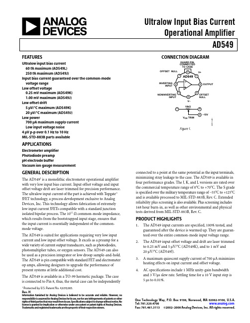
CONNECTION DIAGRAM
GUARD PIN, CONNECTED
TO CASE
OFFSET NULL
8
V+
1 AD549 7
INVERTING INPUT
2
6 OUTPUT
3 NONINVERTING
4. AC specifications include 1 MHz unity-gain bandwidth and 3 V/μs slew rate. Settling time for a 10 V input step is 5 μs to 0.01%.
One Technology Way, P.O. Box 9106, Norwood, MA 02062-9106, U.S.A.
Tel: 781.329.4700
Fax: 781.461.3113 ©2002–2008 Analog Devices, Inc. All rights reserved.
元器件交易网
AD549
TABLE OF CONTENTS
Features .............................................................................................. 1 Applications....................................................................................... 1 Connection Diagram ....................................................................... 1 General Description ......................................................................... 1 Product Highlights ........................................................................... 1 Revision History ............................................................................... 2 Specifications..................................................................................... 3 Absolute Maximum Ratings............................................................ 5
ADS5493EVM;中文规格书,Datasheet资料

User's GuideSLAU325–September2010ADS5493EVM Evaluation Module This evaluation module(EVM)user's guide gives an overview of the ADS5493EVM and provides a general description of the features and functions to be considered while using this module.Contents1Evaluation Module Description (2)2Software Installation (3)3ADS5493EVM Software–SPI Control (4)4Initial EVM Setup and Basic Test Procedure (5)5Power Supply Options (6)List of Figures1ADS5493EVM Overview (2)2Installation Process of ADS5493EVM Software (3)3EVM Software Front Panel (4)4EVM Software Advanced Tab (4)5Basic EVM Hardware Setup (5)6Schematic Modification of the Analog Input Path (5)7Typical Performance Screenshot (6)8Power Supply Options on the ADS5493EVM (6)1 SLAU325–September2010ADS5493EVM Evaluation Module Submit Documentation FeedbackGND Analog InputSignal Clock InputPower SupplyJumper OptionsEvaluation Module Description 1Evaluation Module DescriptionThe ADS5493evaluation module (EVM)is easy to set up and provides the user flexibility.On the analog side,the user can evaluate different transformers and configurations while the EVM also allows asingle-ended or differential clock input.The EVM is powered from a single 5-V power input;the user can select either LDO or switching regulator option for generating the analog and digital 3.3-V supplies for the ADS5493.On the digital side,the EVM provides a seamless interface to the TSW1200capture card in order toevaluate received data directly on a personal computer (PC).The internal registers of the ADS5493can be conveniently accessed and programmed via SPI through the USB connection using the GUI or the TSW1200.The ADS5493EVM works well in default configuration;no register programming is required.Figure 1.ADS5493EVM Overview2ADS5493EVM Evaluation ModuleSLAU325–September 2010Submit Documentation Feedback Software Installation 2Software Installation1.Open the folder named ADS5493_Installer_vxpx (xpx represents the latest version).2.Run Setup.exe.3.Follow the on-screen instructions.4.Once installed,launch by clicking on the ADS5493_GUI_vxpx program in Start >Texas InstrumentsADCs.5.When plugging in the USB cable for the first time,you are prompted to install the USB drivers for USBSerial Converter and USB Serial Port (see Figure 2).(a)Follow the on-screen instructions to install the USB drivers.(b)If needed,you can access the drivers directly in the install directoryFigure 2.Installation Process of ADS5493EVM Software2.1ADS5493.ini file for TSW1200The ADS5493software package comes with a new ini file for the TSW1200.Manually place thisADS5493.ini file into the following directory in order for the TSW1200to recognize it:C:\Program Files\Texas Instruments\TSW1200\ADC Files3SLAU325–September 2010ADS5493EVM Evaluation ModuleSubmit Documentation FeedbackTabs to control allregisters as well asindividual registerwrites on‘advanced’pageIndividual controlregistersControl to send or read all registersas well as load or save register files Reset USB port on FTDIchip –required after powerup of ADS5493EVM Warning indication that USBcommunication is not established Summary of current registers being writtenshowing address and data in hex format‘Advanced’TabOption to write toindividual registers directlyADS5493EVM Software –SPI Control 3ADS5493EVM Software –SPI ControlThe ADS5493is fully functional without the need for register writes;however,the EVM software provides register access to the user.The ADS5493EVM software controls the ADS5493via SPI register writes through a USB connection with the PC.Figure 3is a snapshot of the GUI front panel,highlighting the two tabs to control the setup ofADS5493.It is necessary to perform a USB reset after applying power to the EVM to establish proper connection with the PC.Otherwise,a warning sign on the bottom right flashes,indicating a USB communicationfailure.The EVM software also provides the option to save all registers to a file or to load registers from a file.The display in the bottom right corner provides a summary of all the registers being currently written.Figure 3.EVM Software Front PanelThe Advanced tab allows the user to access the SPI registers directly using individual register writes.Figure 4.EVM Software Advanced Tab4ADS5493EVM Evaluation ModuleSLAU325–September 2010Submit Documentation FeedbackAinClock Initial EVM Setup and Basic Test Procedure 4Initial EVM Setup and Basic Test ProcedureThe fastest way to get the ADS5493EVM up and running is to follow this operating procedure:1.Two signal generators must be connected to the clock and data input of the EVM –preferably withband-pass filter and the 10-MHz reference locked for coherency2.The TSW1200capture card must be plugged in ADS5493EVM and connected to the PC via USB.3.All appropriate power supplies must be connected.4.After performing a USB reset in the ADS5493EVM software,the flashing USB warning signdisappears,indicating successful USB communication.Figure 5.Basic EVM Hardware SetupThe analog input path has a 8.2-pF differential input capacitor at the analog inputs of the ADC as shown in the EVM schematic.This capacitor helps to boost the SFDR performance at higher input frequencies (>50MHz)but is less effective at lower input frequencies.Figure 6.Schematic Modification of the Analog Input PathIn the TSW1200,the ADC selection must be set to ADS5493.Figure 7shows a typical performance plot at 100-MHz IF with a sample rate of 130Msps.In this specific setup,SNR is expected to be in the range of 74–76dBFS whereas SFDR is expected to be better than 91dBc.5SLAU325–September 2010ADS5493EVM Evaluation ModuleSubmit Documentation FeedbackPower Supply Options Figure 7.Typical Performance Screenshot5Power Supply OptionsThe ADS5493EVM is designed to operate from an external 5-V supply,which also connects to the 5-V analog supply of the ADS5493.The user has the option to generate the 3.3V for the analog and digital supplies of the ADS5493either with a LDO (TPS79533)or a switching regulator (TPS62237)by setting jumper JP2and JP3accordingly.The EVM also provides additional pin headers so that the individual voltages for 5V VDDA,3.3V VDDA and 3.3V DVDD can be supplied directly,e.g.,for accurate power consumption measurements.6ADS5493EVM Evaluation ModuleSLAU325–September 2010Submit Documentation FeedbackEvaluation Board/Kit Important NoticeTexas Instruments(TI)provides the enclosed product(s)under the following conditions:This evaluation board/kit is intended for use for ENGINEERING DEVELOPMENT,DEMONSTRATION,OR EVALUATION PURPOSES ONLY and is not considered by TI to be a finished end-product fit for general consumer use.Persons handling the product(s)must have electronics training and observe good engineering practice standards.As such,the goods being provided are not intended to be complete in terms of required design-,marketing-,and/or manufacturing-related protective considerations, including product safety and environmental measures typically found in end products that incorporate such semiconductor components or circuit boards.This evaluation board/kit does not fall within the scope of the European Union directives regarding electromagnetic compatibility,restricted substances(RoHS),recycling(WEEE),FCC,CE or UL,and therefore may not meet the technical requirements of these directives or other related directives.Should this evaluation board/kit not meet the specifications indicated in the User’s Guide,the board/kit may be returned within30 days from the date of delivery for a full refund.THE FOREGOING WARRANTY IS THE EXCLUSIVE WARRANTY MADE BY SELLER TO BUYER AND IS IN LIEU OF ALL OTHER WARRANTIES,EXPRESSED,IMPLIED,OR STATUTORY,INCLUDING ANY WARRANTY OF MERCHANTABILITY OR FITNESS FOR ANY PARTICULAR PURPOSE.The user assumes all responsibility and liability for proper and safe handling of the goods.Further,the user indemnifies TI from all claims arising from the handling or use of the goods.Due to the open construction of the product,it is the user’s responsibility to take any and all appropriate precautions with regard to electrostatic discharge.EXCEPT TO THE EXTENT OF THE INDEMNITY SET FORTH ABOVE,NEITHER PARTY SHALL BE LIABLE TO THE OTHER FOR ANY INDIRECT,SPECIAL,INCIDENTAL,OR CONSEQUENTIAL DAMAGES.TI currently deals with a variety of customers for products,and therefore our arrangement with the user is not exclusive.TI assumes no liability for applications assistance,customer product design,software performance,or infringement of patents or services described herein.Please read the User’s Guide and,specifically,the Warnings and Restrictions notice in the User’s Guide prior to handling the product.This notice contains important safety information about temperatures and voltages.For additional information on TI’s environmental and/or safety programs,please contact the TI application engineer or visit /esh.No license is granted under any patent right or other intellectual property right of TI covering or relating to any machine,process,or combination in which such TI products or services might be or are used.FCC WarningThis evaluation board/kit is intended for use for ENGINEERING DEVELOPMENT,DEMONSTRATION,OR EVALUATION PURPOSES ONLY and is not considered by TI to be a finished end-product fit for general consumer use.It generates,uses,and can radiate radio frequency energy and has not been tested for compliance with the limits of computing devices pursuant to part15 of FCC rules,which are designed to provide reasonable protection against radio frequency interference.Operation of this equipment in other environments may cause interference with radio communications,in which case the user at his own expense will be required to take whatever measures may be required to correct this interference.EVM Warnings and RestrictionsIt is important to operate this EVM within the input voltage range of-0.3V to5.3V and the output voltage range of-0.3V to3.6V. Exceeding the specified input range may cause unexpected operation and/or irreversible damage to the EVM.If there are questions concerning the input range,please contact a TI field representative prior to connecting the input power.Applying loads outside of the specified output range may result in unintended operation and/or possible permanent damage to the EVM.Please consult the EVM User's Guide prior to connecting any load to the EVM output.If there is uncertainty as to the load specification,please contact a TI field representative.During normal operation,some circuit components may have case temperatures greater than50°C.The EVM is designed to operate properly with certain components above25°C as long as the input and output ranges are maintained.These components include but are not limited to linear regulators,switching transistors,pass transistors,and current sense resistors.These types of devices can be identified using the EVM schematic located in the EVM User's Guide.When placing measurement probes near these devices during operation,please be aware that these devices may be very warm to the touch.Mailing Address:Texas Instruments,Post Office Box655303,Dallas,Texas75265Copyright©2010,Texas Instruments IncorporatedIMPORTANT NOTICETexas Instruments Incorporated and its subsidiaries(TI)reserve the right to make corrections,modifications,enhancements,improvements, and other changes to its products and services at any time and to discontinue any product or service without notice.Customers should obtain the latest relevant information before placing orders and should verify that such information is current and complete.All products are sold subject to TI’s terms and conditions of sale supplied at the time of order acknowledgment.TI warrants performance of its hardware products to the specifications applicable at the time of sale in accordance with TI’s standard warranty.Testing and other quality control techniques are used to the extent TI deems necessary to support this warranty.Except where mandated by government requirements,testing of all parameters of each product is not necessarily performed.TI assumes no liability for applications assistance or customer product design.Customers are responsible for their products and applications using TI components.To minimize the risks associated with customer products and applications,customers should provide adequate design and operating safeguards.TI does not warrant or represent that any license,either express or implied,is granted under any TI patent right,copyright,mask work right, or other TI intellectual property right relating to any combination,machine,or process in which TI products or services are rmation published by TI regarding third-party products or services does not constitute a license from TI to use such products or services or a warranty or endorsement e of such information may require a license from a third party under the patents or other intellectual property of the third party,or a license from TI under the patents or other intellectual property of TI.Reproduction of TI information in TI data books or data sheets is permissible only if reproduction is without alteration and is accompanied by all associated warranties,conditions,limitations,and notices.Reproduction of this information with alteration is an unfair and deceptive business practice.TI is not responsible or liable for such altered rmation of third parties may be subject to additional restrictions.Resale of TI products or services with statements different from or beyond the parameters stated by TI for that product or service voids all express and any implied warranties for the associated TI product or service and is an unfair and deceptive business practice.TI is not responsible or liable for any such statements.TI products are not authorized for use in safety-critical applications(such as life support)where a failure of the TI product would reasonably be expected to cause severe personal injury or death,unless officers of the parties have executed an agreement specifically governing such use.Buyers represent that they have all necessary expertise in the safety and regulatory ramifications of their applications,and acknowledge and agree that they are solely responsible for all legal,regulatory and safety-related requirements concerning their products and any use of TI products in such safety-critical applications,notwithstanding any applications-related information or support that may be provided by TI.Further,Buyers must fully indemnify TI and its representatives against any damages arising out of the use of TI products in such safety-critical applications.TI products are neither designed nor intended for use in military/aerospace applications or environments unless the TI products are specifically designated by TI as military-grade or"enhanced plastic."Only products designated by TI as military-grade meet military specifications.Buyers acknowledge and agree that any such use of TI products which TI has not designated as military-grade is solely at the Buyer's risk,and that they are solely responsible for compliance with all legal and regulatory requirements in connection with such use. TI products are neither designed nor intended for use in automotive applications or environments unless the specific TI products are designated by TI as compliant with ISO/TS16949requirements.Buyers acknowledge and agree that,if they use any non-designated products in automotive applications,TI will not be responsible for any failure to meet such requirements.Following are URLs where you can obtain information on other Texas Instruments products and application solutions:Products ApplicationsAmplifiers Audio /audioData Converters Automotive /automotiveDLP®Products Communications and /communicationsTelecomDSP Computers and /computersPeripheralsClocks and Timers /clocks Consumer Electronics /consumer-appsInterface Energy /energyLogic Industrial /industrialPower Mgmt Medical /medicalMicrocontrollers Security /securityRFID Space,Avionics&/space-avionics-defenseDefenseRF/IF and ZigBee®Solutions /lprf Video and Imaging /videoWireless /wireless-appsMailing Address:Texas Instruments,Post Office Box655303,Dallas,Texas75265Copyright©2010,Texas Instruments Incorporated分销商库存信息: TIADS5493EVM。
MAX5499ETE资料
MAX5496 MAX5497
H2
L2
Applications
2
3
4
6 5
-40°C to +85°C 16 TQFN-EP* -40°C to +85°C 16 TQFN-EP*
1 CS
2 W2
3 L2
4 D.N.C.
*EP = Exposed pad. Ordering Information continued at end of data sheet. Selector Guide appears at end of data sheet. SPI is a trademark of Motorola, Inc.
5mm × 5mm × 0.8mm TQFN
Pin Configurations continued at end of data sheet. 1
________________________________________________________________ Maxim Integrated Products
Features
♦ Wiper Position Stored in Nonvolatile Memory and Recalled Upon Power-Up ♦ 16-Pin, 5mm x 5mm x 0.8mm TQFN Package ♦ 35ppm/°C End-to-End Resistance Temperature Coefficient ♦ 5ppm/°C Ratiometric Temperature Coefficient ♦ 10kΩ and 50kΩ End-to-End Resistor Values ♦ 3-Wire SPI-Compatible Serial Interface ♦ Reliability (TA = +85°C) 50,000 Wiper Store Cycles 50 Years Wiper Data Retention ♦ 1.5µA (max) Standby Current ♦ Single +2.7V to +5.25V Supply Operation ♦ Dual ±2.5V Supply Operation
FMMT549ATA;FMMT549TA;FMMT549ATC;FMMT549TC;中文规格书,Datasheet资料

A Product Line ofDiodes Incorporated30V PNP SILICON PLANAR HIGH VOLTAGE TRANSISTOR IN SOT23Features and Benefits • BV CEO > -30V• Maximum Continuous Collector Current I C = -1A• 500mW power dissipation • Complementary type: o FMMT549 – FMMT449 o FMMT549A – N/A • Lead Free, RoHS Compliant (Note 1)• Halogen and Antimony Free "Green" Device (Note 2)• Qualified to AEC-Q101 Standards for High ReliabilityMechanical Data• Case: SOT23 • UL Flammability Rating 94V-0 • Case material: molded Plastic. • Moisture Sensitivity: Level 1 per J-STD-020• Terminals: Matte Tin Finish; Solderable per MIL-STD-202, Method 208• Weight: 0.008 grams (Approximate)Ordering Information (Note 3)Product Marking Reel size (inches) Tape width (mm) Quantity per reel FMMT549TA 549 7 83,000 FMMT549ATA 59A 7 8 3,000Notes:1. No purposefully added lead.2. Diodes Inc.`s “Green” Policy can be found on our website at 3. For Packaging Details, go to our website at .Marking Informationxxx = Product Type Marking Code FMMT549: xxx = 549 FMMT549A: xxx = 59ATop View SOT23 Device Symbol Top View Pin-Out xxxMaximum Ratings @T A = 25°C unless otherwise specifiedCharacteristic Symbol Value UnitCollector-Base Voltage V CBO -35 V Collector-Emitter Voltage V CEO -30 V Emitter-Base Voltage V EBO -5 V Continuous Collector Current I C -1 A Peak Pulse Current I CM -2 A Base Current I B -200 mAThermal Characteristics @T A = 25°C unless otherwise specifiedCharacteristic Symbol Value UnitPower Dissipation (Note 4) P D500 mW Thermal Resistance, Junction to Ambient (Note 4) R θJA250 °C/W Thermal Resistance, Junction to Lead (Note 5) R θJL 197 °C/W Operating and Storage Temperature Range T J, T STG-55 to +150 °CElectrical Characteristics @T A = 25°C unless otherwise specifiedCharacteristic Symbol Min Typ Max Unit Test Condition Collector-Base Breakdown Voltage BV CBO -35 - - V I C = -100µA Collector-Emitter Breakdown Voltage (Note 6) BV CEO -30 - - V I C = -10mA Emitter-Base Breakdown Voltage BV EBO -5 - - V I E = -100µACollector Cutoff Current I CBO- - -0.1 µA V CB = -30V- - -10 V CB = -30V, T A = 100°CEmitter Cutoff Current I EBO - - -0.1 µA V EB = -4VStatic Forward Current Transfer Ratio (Note 6) h FE 70 200 - - I C = -50mA, V CE = -2V80 130 - I C = -1A, V CE = -2V40 80 - I C = -2A, V CE = -2VFMMT549 100 160 300 - I C = -500mA, V CE = -2V FMMT549A 150 200 500 - I C = -500mA, V CE = -2VCollector-Emitter Saturation VoltageV CE(sat) - -250 -500 mV I C = - 1A, I B = -100mA- -500 -750 I C = - 2A, I B = -200mAFMMT549A - - -300mV I C = -100mA, I B = -1mA Base-Emitter Saturation Voltage (Note 6) V BE(sat)- -900 -1250 mV I C = -1A, I B = -100mA Base-Emitter Turn-On Voltage (Note 6) V BE(on)- -850 -1000 mV I C = -1A, V CE = -2V Output Capacitance C obo- - 25 pF V CB = -10V, f = 1MHz Transition Frequency f T100 - - MHz V CE = -5V, I C = -100mA,f = 100MHzSwitching Timest on - 50 - ns I C = -500mA, V CC = -10VI B1 = I B2 = -50mA t off- 300 - ns Notes:4. For a device surface mounted FR4 PCB with minimum recommended pad layout; high coverage of single sided 1 oz copper, in still air conditions; thedevice is measured when operating in a steady-state condition.5. Thermal resistance from junction to solder-point (at the end of the collector lead).6.Measured under pulsed conditions. Pulse width ≤ 300 µs. Duty cycle ≤ 2%Typical Electrical CharacteristicsPackage Outline DimensionsSuggested Pad LayoutSOT23Dim Min Max Typ A 0.37 0.51 0.40 B 1.20 1.40 1.30 C 2.30 2.50 2.40 D 0.89 1.03 0.915 F 0.45 0.60 0.535 G 1.78 2.05 1.83 H 2.80 3.00 2.90 J 0.0130.10 0.05 K 0.903 1.10 1.00 K1 - - 0.400 L 0.45 0.61 0.55 M 0.0850.18 0.11α0° 8° - All Dimensions in mmDimensions Value (in mm)Z 2.9 X 0.8 Y 0.9C2.0 E1.35 X EYCZ分销商库存信息:DIODESFMMT549ATA FMMT549TA FMMT549ATC FMMT549TC。
BC549中文资料
CONDITIONS note 1
VALUE 250
UNIT K/W
CHARACTERISTICS Tj = 25 °C unless otherwise specified.
SYMBOL ICBO
IEBO hFE
VCEsat
VBEsat
VBE
Cc Ce fT F
PARAMETER collector cut-off current
emitter cut-off current DC current gain
BC549C; BC550C
collector-emitter saturation voltage
base-emitter saturation voltage
base-emitter voltage
collector capacitance emitter capacitance transition frequency
Product specification
BC549; BC550
DEFINITIONS
Data Sheet Status
Objective specification Preliminary specification Product specification
This data sheet contains target or goal specifications for product development. This data sheet contains preliminary data; supplementary data may be published later. This data sheet contains final product specifications.
AD芯片大全.docx

AD 系列芯片1. 模数转换器…AD7731BN 24 位 X-△模数转换器(工业级) DIPAD779JD 14位128KSPS 采样速率并行输出模数转换器(民用级) DIP AD7820KN 8位500KSPS 采样速率模数转换器(民用级) DIPAD7821KN 8位1MSPS 采样速率模数转换器(民用级) DIPAD7822BN 8位2MSPS 采样速率模数转换器(工业级) DIPAD7824BQ 8位四通道高速模数转换器(民用级) DIPAD7824KN 8位四通道高速模数转换器(工业级)DIPAD7856AN 14位8通道285KSPS 采样速率模数转换器(工业级)DIPAD7862AN-10 12 位 4 通道同时采样 250KSPS 速率模数转换器 带 2SHA and 2ADC (工业级)DIPAD7864AS-1 12 位4通道同时采样147KSPS 速率模数转换器 (工业级) PQFPAD7865AS-1 14位 4 通道同时采样 175KSPS 速率模数转换器 带 2SHA and 2ADC (工业级)PQFPAD7872AN 14 位 串行输出模数转换器(工业级)DIPAD7891AP-1 12位四通道同时采样模数转换器(工业级) DIPAD7892AN-1 12位四通道同时采样模数转换器(工业级)SOICAD7895AN-10 12位750KSPS 采样速率模数转换器(民用级) DIPAD7874AN 12位750KSPS 采样速率模数转换器(民用级)DIPAD7874BR 12位8通道200KSPS 速率模数转换器 (工业级) SOICAD7886JD 12位单电源八通道串行采样模数转换器(工业级) DIPAD7886KD 12位单电源八通道串并行采样模数转换器(工业级)AD1380JD 16 AD1380KD 16AD1671JQ 12 AD1672AP 12 AD1674JN 12 AD1674AD 12 AD570JD/+ 8 AD574AJD 12 AD574AKD 12 AD578KN 12 AD6640AST 12AD6644AST 14AD676JD 16AD676JN 16AD676KD 16 AD677AR 16 AD677JD 16 AD677JN 16 AD678JD 12 AD678KN 12 AD679JN 14 AD679KN 14AD7660AST 16 AD7664AST 16 AD7701AN 16 位20us 高性能模数转换器(民用级) 位20us 高性能模数转换器(民用级) 位1.25MHz 采样速率带宽2MHz 模数转换器(民用级) 位3MHz 采样速率带宽20MHz 单电源模数转换器(工业级) 位100KHz 采样速率带宽500KHz 模数转换器(民用级) 位100KHz 采样速率带宽 位25us 模数转换器(民用) 位25us 模数转换器(民用) 位25us 模数转换器(民用) 位3us 模数转换器(民用) 500KHz 模数转换器 DIP DIP DIP DIP (工业级) 位65MSPS 模数转换器(工业级)LQFP位65MSPS 模数转换器(工业级)LQFP采样速率并行输出模数转换器(民用级) 采样速率并行输出模数转换器(民用级) 采样速率并行输出模数转换器(民用级) 采样速率串行输出模数转换器 采样速率串行输出模数转换器 采样速率串行输出模数转换器 采样速率并行输出模数转换器 位 100KSPS 位 100KSPS位 100KSPS 位 100KSPS 位 100KSPS 位 100KSPS 位 200KSPS 位 200KSPS 位 128KSPS 位 128KSPS(民用级) (民用级) (民用级) (民采样速率并行输出模数转换器(民用级)采样速率并行输出模数转换器(民用级) 采样速率并行输出模数转换器(民用级)LQFP LQFPDIP DIPDIP SOIC DIP DIP DIP DIP DIP DIP DIPAD7703BN 20 DIPAD7705BR 16 DIPAD7707BR 16 DIPAD7711AN 24 DIPAD7713AN 24 电源 AD7714AN-5 24 位100KSPS CMOS 模数转换器(工业级) 位570KSPS CMOS 模数转换器(工业级) X-△模数转换器(工业级) X-X 模数转换器 X-△模数转换器 X-△模数转换器 X-X 模数转换器 位 位 位 位 (工业级) (工业级) (工业级) (工业级) DIPAD7703AN 20 位 刀-△模数转换器(工业级)位X-△模数转换器(工业级) 位X-△模数转换器(工业级) 位X-△模数转换器(工业级) 位X-△模数转换器(工业级) 位X-△模数转换器(工业级)DIP 3V 位X-△模数转换器(工 DIPAD7705BN 16 SOICAD7706BN 16 SOICAD7710AN 24 DIPAD7712AN 24 DIPAD7714AN-3 24 业级)DIP 5V 电源 AD7715AR-5 16 位X-△模数转换器 位X-△模数转换器(工业级)DIP 5V 电源AD7715AN-5 16 位X-△模数转换器(工业级) SOIC 5V 电源DIPAD7888AR 12位600KSPS采样模数转换器(工业级)DIPAD7890AN-10 12位单电源200KSPS采样速率模数转换器(工业级)DIPAD9042AST 12位41MSPS模数转换器(工业级) LQFPAD9048JQ 8位35MSPS视频模数转换器(民用级)DIPAD9049BRS 9位30MSPS模数转换器(工业级) SSOPAD9050BR 1位40MSPS模数转换器(工业级)SOICAD9051BRS 1(位60MSPS模数转换器(工业级) SSOPAD9057BRS-40 位40MSPSz B频模数转换器(工业级) SSOPAD9057BRS-60 位60MSPS视频模数转换器(工业级) SSOPAD9058JJ双路8位50MSPS视频模数转换器(民用级) LCCAD9059BRS双路8位60MSPS视频模数转换器(工业级) SSOPAD9066JF双路6位60MSPS视频模数转换器(民用级) SSOPAD9071BR 1位TTL兼容100MSPS模数转换器(工业级)SOIC AD9200ARS 10位20MSPS 模数转换器(工业级)SSOP AD9203ARU 10位40MSPS模数转换器(工业级)TSSOP AD9220AR 12位10MSPS模数转换器(工业级)SOIC AD9221AR 12位1MSPS模数转换器(工业级)SOIC AD9223AR 12位3MSPS模数转换器(工业级)SOIC AD9225AR 12位25MSPS模数转换器(工业级)SOIC AD9226ARS 12位65MSPS模数转换器(工业级)SSOP AD9240AS 14位10MSPS模数转换器(工业级)MQFP AD9243AS 14位3MSPS模数转换器(工业级)MQFP AD9260AS 16位2.5MSPS E - △模数转换器(工业级)MQFPAD9280ARS单电源8位32MSPS模数转换器(工业级)SSOPAD9281ARS单电源8位双路32MSPS模数转换器(工业级)SSOPAD9283BRS-100单电源8位100MSPS模数转换器(工业级)SSOPAD9283BRS-80单电源8位80MSPS模数转换器(工业级)SSOPAD9288BRS-80单电源8位双路80MSPS模数转换器(工业级)SSOPAD976CN 16位100KSPS BiCMOS^行输出模数转换器(工业级)DIP AD976AN 16位100KSPS BiCMOS^行输出模数转换器(工业级)DIP AD976AAN 16位200KSPS BiCMOS^行输出模数转换器(工业级)DIP2. 隔离放大器AD202JN 小型2KHz隔离放大器(民用级)卧式AD202JY 小型2KHz隔离放大器(民用级)立式AD204JN 小型5KHz隔离放大器(民用级)卧式AD261BND-1 数字隔离放大器3. 温度传感器AD22100KT 带信号调理比率输出型温度传感器AD22105AR 可编程温控开关电阻可编程温度控制器SOICAD590JH —55 °C - 150 C测温范围温度传感器TO-52AD590KH —55 C〜150 C测温范围温度传感器TO-52AD592AN 低价格,精密单片温度传感器TO-92AD592BN 低价格,精密单片温度传感器TO-92AD7416AR 片内带D/A 数字输出温度传感器LM35升级品可8片级联(工业级)ADXL105JQC土1g- ± 5g带温度补偿加速度传感器(民用级)QC-14ADXL202AQC+ 2g双路加速度传感器(工业级)QC-144. 数字同步调制器AD9830AST带10位D/A, 25MHz主频直接数字同步调制器(工业级)AD9831AST带10位D/A, 50MHz主频直接数字同步调制器(工业级)AD9832BRU带10位D/A, 25MHz主频直接数字同步调制器(工业级)SOICPQFP PQFP TSSOPAD9850BRS带10位D/A, 125MHz主频直接数字同步调制器(工业级)SSOPAD9851BRS带10位D/A, 180MHz主频直接数字同步调制器(工业级)SSOPAD9852AST带12位D/A, 200MHz主频直接数字同步调制器(工业级)LQFP-80AD9852ASC带散热器带12位D/A , 300MHz主频直接数字同步调制器(工业级)LQFP-80 AD9853AS数字QPSK/16 QAM调整器(工业级)PQFPAD9854AST带12位D/A, 200MHz主频直接数字同步调制器(工业级)LQFP-80AD9854ASC带散热器带12位D/A , 300MHz主频直接数字同步调制器(工业级)LQFP-80 AD7008AP20 带10位D/A , 20MHz 主频直接数字同步调制器(工业级)PLCCAD7008JP-50 带10位D/A , 50MHz主频直接数字同步调制器(民用级)PLCC5.振荡器AD2S99AP 可编程正弦波振荡器(工业级)AD537JH 150KHZ AD537SH 150KHZ AD650JN 1MHz AD650KN 1MHz AD652AQ 2MHz AD654JR 500KHz AD654JN 500KHz集成压频转换器(民用级)集成压频转换器(军用级),电压频率转换器(民用级),电压频率转换器(民用级)PLCCTO-99TO-99DIPDIP,同步电压频率转换器(工业级),低价格电压频率转换器(民用级),低价格电压频率转换器(民用级)DIPSOICDIPAD7741BN单通道输入6MHz压频转换器(工业级)级)DIPAD7750AN两通道乘积/频率转换器电度表专用芯片(工业级)6MHz压频转换器(工业DIPAD7742BN四通道输入DIPAD7755AARS IEC521/1036 标准电度表专用芯片(工业级)DIPADVF32KN 500KH工业标准压频转换器(民用级)DIP6.数模转换器AD420AN-32 16 位单电源4-20mA AD420AR-32 16 位单电源4-20mA AD421BN 16 位环路供电符合HART AD421BR 16 位环路供电符合HART输出数模转换器(工业级)输出数模转换器(工业级)输出数模转换器(工业级)输出数模转换器(工业级)(民用)(民用)DIPDIPDIP )DIPDIPDIPDIP协议4-20mA协议4-20mAAD557JN 微处理器兼容完整7位电压输出数模转换器AD558JN 微处理器兼容完整8位电压输出数模转换器AD565AJD 12 AD568JQ 12 AD569JN 16 AD660AN 16 AD667JN 12 AD667KN 12 AD669AN 16位0.25us电流输出数模转换器(民用)超高速电流输出数模转换器(民用)电流输出数模转换器(民用)I 串并行输入数模转换器(工业级)并行输入数模转换器(民用级)并行输入数模转换器(民用级)并行输入数模转换器(工业级)8位数模转换器DIPDIP位位位位3us8us3us位3us位8usAD670JN 单电源,内带仪表放大器电压基准源AD7111ABN 0.37dbAD7111LN 0.37dbAD7224KN 8AD7226KN 8AD7228ABN 8AD7237AAN 12AD7237JN 12AD7243AN 12AD7245AAN 12AD7249BN 12DIPSOICDIPSOIC DIPDIP(民用级)DIP对数数模转换器(工业级)对数数模转换器(工业级)位3us转换时间电压输出数模转换器(民用级)位4通道3us转换时间电压输出数模转换器(民用级)DIP位8通道5us转换时间电压输出数模转换器(工业级)位2通道5us转换时间电压输出数模转换器(工业级)位2通道5us转换时间电压输出数模转换器(民用级)位电压输出型数模转换器(工业级)位10us转换时间电压输出数模转换器位双路串行输出数模转换器(工业级)DIP (工业级)DIPAD7520LN 10 位CMOS数模转换器(民用级)DIPAD7523JN 8 AD7524JN 8 AD7528JN 8 位CMOS数模转换器(民用级)DIP位CMOS带锁存数模转换器(民用级)DIP 位180ns电流输出CMOS数模转换器(民用级)AD7528KN 8 位180ns电流输出CMOS数模转换器(民用级)DIPDIPDIPDIPDIPDIPDIPAD7533JN 10 位600ns电流输出CMOS数模转换器(民用级)DIPAD7535JN 14 位1.5us电流输出CMOS数模转换器(民用级)DIPAD7537JN 12 位双路1.5us电流输出CMOS数模转换器(民用级)DIP AD7541AKN 12 位600ns电流输出CMOS数模转换器(民用级)DIP AD7542JN 12 位250ns电流输出CMOS数模转换器(民用级)DIPAD7543KN 12 位串行输入CMOS数模转换器(民用级)DIPAD7545AKN 12 位1us电流输出CMOS数模转换器(民用级)DIPAD7564BN 低功耗四路数模转换器(工业级)DIPAD7574JN 8 位15us电流输出CMOS数模转换器(民用级)DIPAD767JN 12 位高速电压输出数模转换器(民用级)DIPAD768AR 16 位高速电流输出数模转换器(民用级)SOICAD7837AN 12位双路乘法数模转换器(工业级)DIPAD7845JN 12位乘法数模转换器位电压输出数模转换器(民用级)DIPAD7847AN 12位双路乘法数模转换器(工业级)电源双路电流输出型数模转换器(工业级)DIPAD9708ARU 8位100MSPS双路数模转换器(工业级)TSSOPAD9709AST 8位125MSPS双路数模转换器(工业级)PQFPAD9713BAN 12位80MSPS TTL兼容数模转换器(工业级)DIPAD9721BR 10位400MSPS TTL兼容数模转换器(工业级)SOICAD9731BR 10位170MSPS双电源数模转换器(工业级)SOICAD9732BRS 10位200MSPS单电源数模转换器(工业级)SSOPAD9750AR 10位125MSPS数模转换器(工业级)SOICAD9752AR 12位125MSPS数模转换器(工业级)SOICAD9760AR 10位100MSPS数模转换器(工业级)SOICAD9762AR 12位100MSPS数模转换器(工业级)SOICAD9764AR 14位100MSPS数模转换器(工业级)SOICAD9772AST 14位300MSPS数模转换器(工业级)LQFPAD977AAN 16位200KSPS BiCMOSl行输出数模转换器(工业级)DIPAD977AN 16位100KSPS BiCMOSl行输出数模转换器(工业级)DIP7. 运放AD515AJH 低价格,低偏置电流,高输入阻抗运放(民用级)TO-99AD515ALH 低价格,低偏置电流,高输入阻抗运放(民用级)TO-99AD517JH 低失调电压,高性能运放(民用级)TO-99AD518JH 宽带,低价格运放(民用级)TO-99AD521JD 电阻设置增益精密仪表放大器(民用级)DIPAD524AD 引脚设置增益高精度仪表放大器(工业级)DIPAD526BD 软件编程仪表放大器(工业级)DIPAD526JN 软件编程仪表放大器(民用级)DIPAD542JH 低价格,低偏置电流,高输入阻抗运放(民用级)TO-99AD545ALH 低偏置电流,高输入阻抗运放(民用级)TO-99AD546JN 静电计放大器(民用级)DIPAD547JH 低价格,低偏置电流,高输入阻抗运放(民用级)TO-99AD548JN 精密BiFET输入运放(民用级)DIPAD549JH 低偏置电流,高输入阻抗运放(民用级)TO-99AD549LH 低偏置电流,高输入阻抗运放(民用级)TO-99AD5539JN 高速运放(民用级)DIPAD582KD 0.7us 采样保持放大器(民用)DIPAD585AQ 3us 采样保持放大器(工业级)DIPAD684JQ 1us 四通道采样保持放大器(民用级)DIPAD781JN 700ns采样保持放大器(民用级)DIPAD9101AR 7ns建立时间采样保持放大器低噪声宽带可变增益双运放(民用级)DIP (民用级)DIPAD7846JN16 DIPAD8522AN 12 位(工业级)SOICAD600XNAD602JN 低噪声宽带可变增益双运放(民用级)DIPAD603AQ 低噪声可变增益运放(工业级)DIPAD606JN 50M Hz, 80db 对数放大器(民用级)DIPAD620AN 低功耗仪表放大器(工业级)DIPAD621AN 低功耗仪表放大器(工业级)DIPAD622AN 单电源仪表放大器(工业级)DIPAD623AN 单电源Rail-Rail输出仪表放大器(工业级)DIP AD623AR 单电源Rail-Rail输出仪表放大器(工业级)SOIC AD624AD 精密仪表放大器(工业级)DIPAD625JN 可编程增益仪表放大器(民用级)DIPAD625KN 可编程增益仪表放大器(民用级)DIPAD626AN 单电源仪表放大器(工业级)DIPAD627AN 单电源低功耗Rail-Rail输出仪表放大器(工业级)DIP AD629AN 高电压抑制比差分放大器(工业级)DIPAD648JN 精密,BiFET输入运放(民用级)DIPAD704JN 精密四运放(民用级)DIPAD705JN 精密运放(民用级)DIPAD706JN 精密双运放(民用级)DIPAD707AQ 精密单运放(工业级)DIPAD707JN 精密单运放(民用级)DIPAD708AQ 双AD707 (工业级)DIPAD708JN 双AD707 (民用级)DIPAD711AQ 精密BiFET输入运放(工业级)DIPAD711JR 精密BiFET输入运放(民用级)SOICAD711JN 精密BiFET输入运放(民用级)DIPAD712AQ 双AD711 (工业级)DIPAD712JN 双AD711 (民用级)DIPAD713BQ 四AD711 (工业级)DIPAD713JN 四AD711 (民用级)DIPAD741KN 通用运放(民用级)DIPAD743JN 低噪声,BiFET输入运放(民用级)DIPAD744JN 精密,双极性运放(民用级)DIP AD745JN 精密低噪声运放(民用级)DIPAD790JN高速精密比较器(民用级)DIPAD795JN低偏置电流低噪声运放(民用级)DIPAD797A N低失真低噪声运放(工业级)DIPAD797AR低失真低噪声运放(工业级)SOICAD8001AN 800MHz电流反馈运放(工业级)DIPAD8002AN 800MHz电流反馈双运放(工业级)DIPAD8009AR 1GHz 4500V/US电流反馈双运放(工业级)DIPAD8011AN 340MHz电流反馈运放(工业级)DIPAD8015AR单电源真空管前置放大器(工业级)SOICAD8031AN单电源Rail-Rail 输入输出运放(工业级)DIPAD8032AN单电源Rail-Rail 输入输出双运放(工业级)DIPAD8036AN低失真宽带240MHz电压输出运放(工业级)DIPAD8037AN低失真宽带270MHz电压输出运放(工业级)DIPAD8041AN 120MH带宽Rail-Rail 输出运放(工业级)DIPAD8041AR 120MHz带宽Rail-Rail 输出运放(工业级)SOICAD8042AN 120MH带宽Rail-Rail 输出双运放(工业级)DIPAD8044AN 80MHz带宽Rail-Rail 输出四运放(工业级)DIPAD8047AN电压反馈运放(工业级)DIPAD8055AR 电压反馈运放(工业级)SOICAD8056AR低价格300MHz电压反馈双运放(工业级)SOICAD8058AR电压反馈双运放(工业级)SOICAD840JN宽带高速运放(民用级)DIPAD843AQ 34MHz带宽高速FET输入运放(工业级)DIPAD844AN 2000V/us高速运放(工业级)DIPAD845JN 16MHz带宽高速FET输入运放(民用级)DIPAD845KN 16MHz带宽高速FET输入运放(民用级)DIPAD817AN高速低功耗宽电源运放(工业级)DIPAD847AQ 300V/US高速低功耗运放(工业级)DIPAD847JN 300V/US高速低功耗运放(民用级)DIPAD847SQ 300V/us高速低功耗运放(军用级)DIPAD849JN高速低功耗运放(民用级)DIPAD8551AR自稳零运放(工业级)SOICAD8552AR自稳零双运放(工业级)SOICAD8561AN单电源比较器(工业级)DIPAD8561AR单电源比较器(工业级)SOICAD8564AN单电源TTL/CMOS3路比较器(工业级)DIPAD8598AN单电源双路比较器(工业级)DIPAD8350AR15差分输入射频放大器(工业级)SOICAD818AN低价格高速电压反馈视频运放(工业级)DIPAD820AN单电源低功耗FET输入Rail-Rail 输出运放(工业级)DIPAD822AN双AD820(工业级)DIPAD822AN-3V 双AD820(工业级)DIP 3V 电源AD823AN单电源Rail-Rail 输出双运放(工业级)DIPAD824AN单电源Rail-Rail 输出四运放(工业级)DIPAD826AN高速低功耗双运放(工业级)DIPAD827AQ 双AD847 (工业级)DIPAD827JN 双AD847 (民用级)DIPAD828AN 双AD818(工业级)DIPAD829JN高速低噪声视频运放(工业级)DIPAD8307AN 500MHz对数放大器(工业级)DIPAD8307AR 500MH 对数放大器(工业级)SOICAD8309ARU 500MH对数放大器(工业级)TSSOPAD830A高速视频差动运放(工业级)DIPAD8313ARM 2.5GHz对数放大器(工业级)RM-8AD830AN高速视频差动运放(工业级)DIPAD8313ARM 2.5GHz对数放大器(工业级)RM-8AD8320ARP数字可变增益线性驱动器(工业级)RP-20AD811AN 高性能视频运放(工业级)DIPAD811JR 高性能视频运放(工业级)SOICAD812AN 低功耗电流 反馈双运放(工业级)DIPAD812AR 低功耗电流反馈双运放(工业级)SOICAD8131AR 差分输入输出 电压反馈放 大器(工业级) SOICAD8138AR IF 放大器(工业级) SOICAD813AN 单电源低功耗三视频运放(工业级)DIPAD813AR-14单电源低功耗三视频运放(工业级)SOICAD815AY 大电流输出,差动输入 输出运放(工业 级)AD810AN 带电源休眠控制端的低功耗视频运放 (工业级)DIPAD8018AR 5V Rail-Rail 大电流输出XDSL 线 性驱动放大器(工业级) SOICAD9617JR 1400V/us,140MHz 带宽高速运放(民用级)SOIC AD9617JN 1400V/us,140MHz 带宽高速运放(民用级)DIPAD9618JN 1800V/us,160MHz 带宽高速运放(民用级)DIP AD9630AN 低失真闭环缓冲放大器(工业级)DIP AD9631AN 超低失真 宽带电压反馈放大器(工业级)DIP AD96687BQ 高速双 电压比较器(工业级)DIPAD9698KN 高速TTL 兼容双 电压比较器(工业级)DIP AMP02FP 高精度仪表放大器(工业级) DIP AMP04FP 单电源精密仪表放大器(工业级) DIP OP07AZ/883C 超低失调电压运放(军用级) DIP OP07CP 超低失调电压运放(工业级) DIPOP07CS 超低失调电压运放(工业级) SOIC OP176GP 低失真低噪声运放(工业级)DIP OP177GP 高精密运放(工业级) DIPOP27GP 低噪声精密运放(工业级) DIP输入输出双运放 输入输出双运放 输入输出双运放 OP297GP 超低偏置电流精密双运放 OP297GS 超低偏置电流精密双运放 OP37EP 低噪声精密运放(民用级)OP37GP 低噪声精密运放(工业级)8. 模拟乘法器AD532JH 模拟乘法器(民用级)TO-99 AD534JD 模拟乘法器(民用级)DIPAD534JH 模拟乘法器(民用级)TO-99 AD538AD 单片实时模拟乘法器(工业级) DIP AD539JN 宽带双通道线性乘法器(民用级)DIP AD633JN 低价格模拟乘法器(民用级) DIPAD734AQ 10MHz 带宽四象限模拟乘法器(工业级)DIPAD834JN 500MHz t 宽四象限模拟乘法器(工业级) DIPAD835AN 250M H 带宽四象限电压输出模拟乘法器(工业 级)DIP9. 有效值直流转换器AD536AJH 集成真有效值直流转换器(民用级)TO-99 AD536AJD 集成真有效值直流转换器(民用级)DIPAD536AJQ 集成真有效值直流转换器(民用级)DIP AD636JH 高精度真有效值直流转换器(民用级) TO-99AD636JD 高精度真有效值直流转换器(民用级) DIP AD637JQ 高精度真有效值直流转换器(民用级) DIP AD736JN 通用真有效值直流转换器(民用级)DIPOP291GP 单电源 Rail-Rail OP295GP 单电源 Rail-Rail DIPDIP DIP(工业级) (工业级) (工业级) (工业级)(工业级) OP495GP 单电源Rail-Rail 输入输出四运放 OP497GP 超低偏置电流精密四运放(工业级) OP77GP OP0改进型(工业级) DIPOP90GP 低电压微功耗精密运放(工业级) OP97FP 微功耗精密运放(工业级) OP97FS 微功耗精密运放(工业级)(工业级) DIP DIP DIPSOICAD737JN 通用真有效值直流转换器(民用级) DIP AD737AQ 通用真有效值直流转换器(工业级)DIP10. 电压基准源AD580JH 精密2.5V 电压基准源(民用级) TO-52 AD580LH 精密2.5V 电压基准源(民用级) TO-52 AD581JH 精密10V 电压基准源(民用级) TO-5 AD584JH 引脚设置输出电压基准源(民用级) TO-99 AD584JN 引脚设置输出电压基准源(民用级) DIPAD586JN 精密5V 电压基准源(民用级) DIP AD586JQ 精密5V 电压基准源(民用级) DIP AD586KN 精密5V 电压基准源(民用级)DIP AD586KQ 精密5V 电压基准源(民用级) DIP AD586KR 精密5V 电压基准源(民用级) SOIC AD587KN 精密10V 电压基准源(民用级)DIP AD587KR 精密10V 电压基准源(民用级)SOIC AD588AQ 精密可编程电压基准源(工业级) DIP AD589JH 精密1.235V 电压基准源(民用级) H-02A AD680JN 精密2.5V 电压基准源(民用级) DIPAD780AN 2.5V 或3V 可选输出高精度电压基准源(工业级) DIP REF02CP 精密5V 电压基准源带温度传感器(工业级) DIP11. 多路转换器和模拟开关AD7501JN 8 选1 CMOS 多路转换器(民用级) DIP AD7502JN 差动4选1 CMOS 多路转换器(民用级) DIP AD7502KQ 差动4选1 CMOS 多路转换器(民用级) DIPAD7503JN 8 选1 CMOS 多路转换器(民用级) DIP AD7506JN 16 选1 CMOS 多路转换器(民用级)DIPREF03GP 精密低价格2.5V 电压基准源(工业级)REF192GP 低功耗 REF192GS 低功耗 REF194GP 低功耗 REF195GS 低功耗 大电流输出 大电流输出 大电流输出 大电流输出 REF43FZ 高精度2.5V 电压基准源(工业级)DIP 2.5V 电压基准源(工业级) 2.5V 电压基准源(工业级) 4.5V 电压基准源(工业级) 5V 电压基准源(工业级) DIP SOIC DIP SOICADG436BN 双单刀单掷模拟开关(工业级) DIP ADG441BN 四单刀单掷模拟开关(工业级) DIP ADG442BN 四单刀单掷模拟开关(工业级) DIPADG506AKN 16选1CM0模拟多路转换器(民用级) DIP ADG507AKN 差动8选1CMOS 模拟多路转换器(民用级) DIP ADG508AKN 8选1CM0模拟多路转换器(民用级) DIPADG508FBN 8选1CM0S 带过压保护模拟多路转换器(工业级) DIP ADG509AKN 差动4选1CMOS 模拟多路转换器(民用级) DIP ADG511BN 单电源四单刀单掷模拟开关(工业级) DIP ADG608BN 8选1CM0模拟多路转换器(工业级) DIPADG609BN 差动4选1CM0模拟多路转换器(工业级) DIP ADG719BRMI 路视频CMOS 模拟开关(工业级)RM-6 ADG736BRMX 路视频CMOS 模拟开关(工业级)RM-1012. 电压电流变送器AD693AQ 环路供电,4〜20mA 输出传感器信号变送器(工业级) DIPAD694AQ 0 〜2V 或0〜10V 输入,4〜20mA 或0-20mA 输出信号变送器(工业级) DIP AD694JN 0 〜2V 或0〜10V 输入,4〜20mA 或0-20mA 输出信号变送器(民用级) DIPAD595AD K 型(铬-铝)热电偶信号调节器(工业级) DIPAD595AQ K 型(铬-铝)热电偶信号调节器(工业级) DIP AD598AD 线性可变位移信号调节器(LVDT )(工业级)DIP AD607ARS 低功耗混频器/AGC/RSSC 3V 接收机的IF 子系统(工业级) SSOP AD630JN 平衡跳制解调器(民用级)DIPAD698AP 通用线性可变位移信号调节器(LVDT )(工业级)PLCCAD720JP RGB-NTSC/PAL 编码器(民用级)PLCC AD722JR-16 Analog toNTSC/PAL 编码器(民用级) S OIC AD724JR Analog toNTSC/PAL 编码器(民用级) SOIC AD75019JP 16 X 16音频距阵开关(民用级) PLCCAD7777AR 10位多路T/H 子系统(工业 级)SOICAD73360AR 16位6通道数据采集子系统(三相电量测量IC )(工业级)SOICAD8079AR 双通道260MHz 缓冲器(工业级)SOICAD8108AST 8X8视频距阵开关(工业级) LQFPAD8109AST8X8视频距阵开关(工业 级)LQFPAD8111AST16X8视频距阵开关(工业级) LQFPAD8115AST16X 16视频距阵开关(工业 级)LQFPAD8116AST16X 16视频距阵开关(工业级) LQFPAD8170AN 2选1视频多路转换器(工业 级)DIPAD8174AN 4选1视频多路转换器(工业级)DIPAD8180AN 差动2选1视频多路转换器(工业级)DIPAD8184AN 4选1视频多路转换器(工业级)DIPAD8402AN-10 2通道数字电位器 阻值10K (工业 级)DIPAD8403AN100 4通道数字电位器 阻值100K (工业级)DIP AD9300KQ 4选1宽带视频多路转换器(民用级)DIPAD7507JN 差动8选1 CMOS 多路转换器(民用级) DIPAD7510DIJN 四单刀单掷 CMOS 介质隔离模拟开关 9民用级) DIP AD7510DIKN 四单刀单掷 CMOS 介质隔离模拟开关 9民用级) DIP AD7512DIJN 双单刀双掷 CMOS 介质隔离模拟开关 9民用级) DIP AD7512DIKN双单刀双掷 CMOS 介质隔离模拟开关 9民用级) DIPAD7590DIKN 四单刀单掷 CMOS 带锁存介质隔离模拟开关 9民用级) ADG201AKN3单刀单掷模拟开关(民用级) DIP ADG201HSJN 四单刀单掷模拟开关(民用级) DIP ADG211AKN3单刀单掷模拟开关(民用级) DIP ADG222AKN3单刀单掷模拟开关(民用级) DIP ADG333ABN3单刀单掷模拟开关(工业级)DIPADG333ABF 四单刀单掷模拟开关(工业级) SOIC ADG408BN 8选1CMO 模拟多路转换器(工业级) DIP ADG409BN 差动4选1CMO 模拟多路转换器(工业级) DIP ADG411BN 四单刀单掷模拟开关(工业级) DIP ADG417BN 单刀单掷模拟开关(工业级) DIP ADG419BN 单刀单掷模拟开关(工业级) DIP ADG431BN 四单刀单掷模拟开关(工业级) DIPDIPAD9483KS-100 8位100MSPS三视频模数转换器(民用级)MQFPAD9500BQ数字化可编程延迟信号发生器(工业级)DIPAD9501JN TTL/COMS数字化可编程延迟信号发生器(民用级)DIP AD9801JCST 10位6MSPS CCD言号处理器(民用级)LQFPAD9802JST 10位6MSPS CCD信号处理器(民用级)LQFPAD9803JST 10位6MSPS CCD信号处理器(民用级)LQFPAD9805JS 10位3通道6MSPS CCD信号处理器(民用级)MQFPAD9816JS 12位3通道6MSPS CCD信号处理器(民用级)MQFP AD9822JR 14位3通道12MSPS CCDB号处理器(民用级)SOICAD9901KQ线性相位探测器/频率鉴别器(民用级)DIPADM660AN DC-D转换器(工业级)DIPADM690AN微处理器监控电路(工业级)DIP ADM708AN微处理器监控电路(工业级)DIPADSP21060KS160 32位浮点数字信号处理器内存4M (民用级)PQFP ADSP21060CZ-160 32位浮点数字信号处理器内存4M (工业级)PQFP ADSP21062KS-160 32位浮点数字信号处理器内存2M (民用级)PQFPADSP2181KS-133 16位定点数字信号处理器(民用级) PQFP-128ADSP2181KST-133 16位定点数字信号处理器(民用级) TQFP-128ADUC812BS 带单片机、8路12位A/D 、2路D/A 的数采系统(工业级) PQFPDAC08CP 8位高速电流输出型数模转换器(民用级)DIP DAC8228FP 8位双路电压输出型数模转换器(工业级)DIPPKD01FP 峰值检测器(工业级) DIPSMP04EP 7us 四通道采样保持放大器(工业级) DIPSMP08FP 7us 八通道采样保持放大器(工业级) DIPSSM2141P 差动线路接收器Gain=OdB (工业级)DIPSSM2142P 平衡线路驱动器(工业级) DIPSSM2143P 差动线路接收器Gain=-6dB (工业级)DIPSSM2211P 1V 功率差分输出音频功率放大器(工业级) DIPSSM2275P Rail-Rail 输出双音频功率放大器(工业级) DIP TMP03FS PW 输出,直接与微处理器接口数字输出温度传感器SOICTMP04FS 反相PWM 输出,直接与微处理器接口数字输出温度传感器 SOIC TMP36GT9电压输出温度传感器 TO-92 MAX 系列芯片MAX038CPP 波形发生器MAX1044CPA60KHz 振荡器自举模式 DC-DC 电荷泵转换器 MAX110ACPE MAX110BCPEMAX111BCPEMAX122BCNGMAX1232CPAMAX1242BCSA 10位带2.5V 基准的串形模数转换器14位2X 4通道4路同时采集并行模数转换器MAX125CEAX MAX134CPL MAX135CPI MAX139CPL MAX140CPL MAX1480BCPI MAX1480BEPI MAX1483CPA RS-485/RS-442 MAX1487CPA RS-485/RS-442MAX1487ECPA RS-485/RS-442MAX1488ECPD RS-232 接口,+15KV 保护MAX1489ECPD RS-232 接口,+15KV 保护MAX148BCPP 低功耗 8 路 10 位 A/DMAX1490BCPG 完全隔离全双IKS-485接口MAX158BCPI 高速 8 路 8 位 A/DMAX1771CPA 开关型DC-DC 变换器MAX1771CSA 开关型DC-DC 变换器低价格双路14位串形模数转换器 低价格双路14位串形模数转换器 低价格14位串形模数转换器 高速带采保和基准的12位模数转换器 微处理器监控电路 积分型A/D 转换器,+5V ,3-3/4位 低功率A/D 转换器积分型A/D 转换器积分型A/D 转换器 完全隔离半双 完全隔离半双 RS-485 接口RS-485 接口接口,256个节点接口,128个节点 接口,+15KV 保护MAX180CCPL 8 路 12 位 A/DMAX186CCPP MAX187BCPA MAX189CCPA MAX191BCNG MAX192BCPP MAX197BCNI12位,八通道故障保护,带采保并行 A/D MAX202CPE RS-232 接口,+5VMAX202CSE RS-232 接口MAX202ECPE + 15KV 静电保护 RS-232 接口MAX202EESE + 15KV 静电保护,工业级 RS-232接口 MAX202EPE 工业级 RS-232 接口MAX207CNG RS-232 接口MAX208CNG RS-232 接口MAX232CPE RS-232 接口 ,+5VMAX232CSE RS-232 接口MAX232EPE 工业级 RS-232 接口MAX235CPG RS-232 接口 5 组收发器MAX238CNG RS-232 接口MAX238ENG RS-232 接口MAX260BCHG 双路,开关电容型4阶滤波器 MAX260BENG 双路,开关电容型4阶滤波器MAX261BCNG 双路,开关电容型4阶滤波器 MAX262BCNG 双路,开关电容型 4阶滤波器 MAX280CPA 单路,开关电容型 5阶滤波器 MAX291CPA 有源滤波器,时钟可编程MAX292CPA 有源滤波器,时钟可编程MAX293CPA 有源滤波器,时钟可编程MAX294CPA 有源滤波器,时钟可编程MAX297CPA 有源滤波器,时钟可编程MAX301CPE 模拟开关MAX305EPE 模拟开关MAX306CPI 模拟多路转换器MAX3080CPD 失效保护 RS-485/RS-232 MAX3082CPA 失效保护 RS-485/RS-232MAX308CPE 模拟多路转换器MAX309CPE 模拟多路转换器MAX3100CPD 通用异步收发信机(UART )MAX312CPE 模拟开关MAX313CPE 模拟开关MAX318CPA 模拟开关MAX319CPA 模拟开关MAX3218CPP RS-232 接口MAX3223CPP RS-232 接口MAX3232CPE RS-232 接口MAX325CPA 模拟开关MAX333CPP 模拟开关MAX338CPE 模拟多路转换器MAX339CPE 模拟多路转换器MAX351CPE 模拟开关MAX354CPE 模拟多路转换器MAX354CWE 模拟多路转换器MAX354EPE 模拟多路转换器(工业级)串行接口 A/D ,带采保,电压基准,12位,采样速率133KHZ串行A/D ,12位,采样速率 75KHZ低功耗,12位单通道,串行带采保和电压基准 A/D 低功耗,12位单通道,带采保和电压基准 A/D 串行A/D ,10位采样速率133MMAX355CPE模拟多路转换器MAX355CWE 模拟多路转换器MAX366CPA模拟多路转换器MAX483CPA RS-485/RS-422 MAX485CPA RS-485/RS-422 MAX487CPA RS-485/RS-422 MAX487ECPA RS-485/RS-422 MAX487EEPA RS-485/RS-422 MAX488CPA RS-485/RS-422 MAX490ECPA RS-485/RS-422MAX491CPD RS-485/RS-422 MAX491ECPD RS-485/RS-422 MAX501AENG D/A 转换器 MAX504CPD 串行,低功耗D/A 转换MAX505BCNG 四路8位D/A 转换MAX506CPP D/A 转换MAX509BCPE D/A 转换MAX512CPD 8 位低功耗 D/AMAX515CPA 电压输出串型 10位D/AMAX517BCPA D/A 转换 二线接口MAX518BCPA 双路 517MAX526DCNG 四路12位D/A 转换MAX527DCNG 土 5V 四路 12 位 D/A 转换MAX367CPN MAX384CPN MAX391CPE MAX400CPA MAX4016ESA MAX4100ESA MAX4101ESA MAX4106ESA MAX4107ESA MAX4142ESD MAX4146ESD MAX419CPD MAX420CPA MAX427CPA MAX435CPD MAX436CPD MAX440CPI MAX441CPP MAX442CPA MAX4456CPL MAX453EPA MAX457EPA MAX458CPL MAX468CPE MAX470CPE MAX479CPDMAX480EPA 模拟多路转换器模拟多路转换器 模拟多路转换器 运算放大器 视频放大器 视频放大器视频放大器 视频放大器 视频放大器 视频放大器视频放大器 运算放大器 运算放大器 运算放大器运算放大器运算放大器 视频多路转换器/放大器 视频多路转换器/放大器 视频多路转换器/放大器视频矩阵开关 视频多路转换器/放大器 视频放大器 视频矩阵开关 视频缓冲器 视频缓冲器 运算放大器运算放大器 接口接口接口接口 接口 接口 接口接口接口MAX528CPP 八路8位D/A转换MAX530BCNG 低功耗D/A转换MAX531BCPD 串行接口,低功耗D/A转换,多种电压输出MAX532BCPE D/A 转换,12 位MAX536BCWE 四路串型电压输出12位D/AMAX538BCPA D/A 转换MAX543ACPA D/A 转换MAX551ACPA 12 位D/A 转换器MAX603CPA 低压差线性稳压器MAX619CPA DC-DC 电荷泵变换器MAX6225ACPA 基准电压源MAX6225AESA 基准电压源MAX6225BCPA 基准电压源MAX6225BCSA 基准电压源MAX622CPA DC-DC 电荷泵变换器MAX6250BCPA 基准电压源MAX633ACPA DC-DC 变换器MAX638AEPA DC-DC 变换器MAX639CPA DC-DC 变换器MAX660CPA DC-DC 电荷泵变换器,振荡频率10KHZ可选择MAX662ACPA DC-DC 变换器,外围仅需3个小电容MAX667CPA低压差线性稳压器MAX691ACPE MP 监控电路MAX691CPE MP监控电路MAX705CPA MP监控电路MAX706CPA MP监控电路MAX708CPA MP监控电路MAX708CSA-T MP 监控电路MAX709LEPA 监控电路MAX712CPE 电池充电器电路MAX712EPE 电池充电器电路MAX713CPE 电池充电器电路MAX7219CNG LED 显示驱动电路MAX7219ENG LED 显示驱动电路MAX724CCK 降压型DC-DC变换器MAX726CCK 降压型DC-DC变换器MAX729CCK 降压型DC-DC变换器MAX730ACPA 降压型DC-DC变换器,单频开关噪音MAX733CPA升压型DC-DC变换器MAX735CPA反向输出DC-DC变换器MAX736CPD 反向输出DC-DC变换器MAX738ACPA 降压型DC-DC变换器,单频开关噪音MAX738AEPA 降压型DC-DC变换器,单频开关噪音MAX739CPD 反向输出DC-DC变换器MAX739CWE 反向输出DC-DC变换器MAX7400CPA有源滤波器。
ad9850中文资料

海纳电子资讯网:www.fpga-arm.com目录摘要 —————————————————————————2 创新之处 ———————————————————————2 关键词 ————————————————————————2 引言 —————————————————————————2 系统工作原理 —————————————————————3 直接数字频率合成 ———————————————————4 DDS 基本原理及性能特点 —————————————————5 采用 DDS 的 AD9851 ———————————————————6 AD9851 的原理 —————————————————————7 AD9851 在信号源中的应用 ————————————————8 AD9851 在本系统的应用电路 ———————————————9 低通滤波器(LPF) ——————————————————10 锁相环频率合成 ———————————————————11 锁相环频率合成 MC145151 在本电路中的应用 ————————12 压控振荡器(VCO) ———————————————————12 缓冲放大器 ——————————————————————13 单片机控制的整体电路 —————————————————14 功率放大 ———————————————————————15 本系统的软件设计 ———————————————————15 总调试 ————————————————————————25 结束语 ————————————————————————25 DDS 短波信号发生器技术指标 ——————————————26 所采用的仪器设备 ———————————————————26 所用软件 ———————————————————————26 参考文献 ———————————————————————26 参考网站 ———————————————————————27www.fpga-ar m1.海纳电子资讯网:www.fpga-arm.comDDS 短波信号发生器摘要: 本文主要介绍的是采用直接数字频率合成的短波信号发生器, 它 主要以微电脑控制部分、直接数字频率合成(DDS)部分、数字锁相 环频率合成部分、背光液晶显示部分、功率放大部分等组成。
EN549中文版
英国标准规范于燃气器具、设备密封件和膜片用橡胶材料欧洲标准EN549 :1994年以来的英国标准未经BSI允许不得拷贝此英国标准责任委员会此英国标准委托GSE/22技术委员会进行编辑,燃气具的安全与控制如下所诉:控制器制造商协会(TAMCA(BEAMA有限公司英国电器制造厂商协会));英国燃气公司(英国)贸工部(消费者安全协会,加利福利亚分部)液化石油气协会英国燃气工业协会修订后出版发行委员会指导编辑,标准委员会权威发行,于1995年5月15日实施。
此后BSI条款涉及工作标准:GSE/22 标准委员会92/82881 DC 征求意见稿前言此英国标准委托GSE/22技术委员会进行编辑,EN 549:1994为英文版,燃气器具、设备密封件和膜片用橡胶材料,由欧洲标准化委员会(CEN)出版。
此标准替代BS 6505。
EN549是由英国积极参加国际讨论后所出版。
互相参照出版物对应英国标准BS(英国国家标准)903 橡胶物性测试ISO48 A26. 硬度确定ISO188 A19. 耐热性与加速老化试验ISO247 BS 7164 原材料与硫化橡胶的化学测试5. 灰分含量的确定方法BS 903 橡胶物性ISO471 A35. 试验片的测试时间、温度、湿度的调节ISO815 A6. 压缩变形的环境、高低温的确定方法ISO1400 A26. 硬度确定ISO1407 BS 1673 橡胶原材料及未加硫复合橡胶的测试方法2.橡胶原材料的化学分析BS 903 橡胶物性测试ISO1431-1 A43. 抗臭氧开裂性确定方法(静态应变测试)ISO1817:1985 A16.1987 液体中效果确定BS 903 橡胶物性测试ISO4648 A38. 用于测试的试验片及产品的尺寸确定方法ISO4650 BS 4181 橡胶红外光谱鉴定1.碳化氢、氯丁二烯、丁腈及氯磺化聚乙烯橡胶的确定方法遵守英国标准,本身并不赋予法律义务的豁免权。
AD549JHZ资料

1. The AD549 input currents are specified, 100% tested, and guaranteed after the device is warmed up. They are guaranteed over the entire common-mode input voltage range.
Ultralow Input Bias Current Operational Amplifier AD549
CONNECTION DIAGRAM
GUARD PIN, CONNECTED
TO CASE
SET NULL
8
V+
1 AD549 7
INVERTING INPUT
2
6 OUTPUT
3 NONINVERTING
2. The AD549 input offset voltage and drift are laser trimmed to 0.25 mV and 5 μV/°C (AD549K), and to 1 mV and 20 μV/°C (AD549J).
3. A maximum quiescent supply current of 700 μA minimizes heating effects on input current and offset voltage.
ESD Caution.................................................................................. 5 Typical Performance Characteristics ............................................. 6 Functional Description .................................................................. 10
ad549中文资料

极低偏置电流运算放大器AD5491 概述AD549是具有极低输入偏置电流的单片电路静电计型运算放大器。
为达到高精度的目的,输入偏置电压和输入偏置电压漂移均通过激光调节。
这种极低输入电流性能由ADI公司专有的topgate工艺技术完成。
该技术可以制造与具有极低输入电流的JFET并与双极性电路隔离的集成运放。
输入级具有1015Ω的共模阻抗,其输入电流与共模电压无关。
AD549适用于低输入电流和低输入偏置电压的场合。
它特别适合用作各种电流输出的传感器,如光电二极管、光电倍增管以及氧气传感器等的前置放大器。
该产品也可用作精密积分器或低衰减采样保持器。
AD549的封装与标准FET和静电计运算放大器兼容,因此用户花少量成本即可对系统升级,提高已有系统的性能。
AD549有TO-99密封封装。
金属外壳与8管脚相连,使得金属外壳与同样电压的输入终端独立连接,达到降低外壳泄漏的目的。
AD549具有四种性能等级。
其中J、K和L型号的温度范围是0℃到70℃。
S型号专用于军事,其温度范围:-55℃到125℃。
AD549的输入电流在整个共模输入电压范围内都得到保证,其输入失调电压和漂移由激光分别调节到和5μV/℃(AD549K);1mV和20μV/℃(AD549J)。
700μA的最大静态电流使输入电流和偏置电压的热效应降到最低。
模拟性能包括1MHz的均匀增益带宽和3V/μs的压摆率。
当输入为10V时,建立时间是5μs 到%。
2 AD549的引脚及特性参数图一所示是AD549的引脚图,表一所示是其特性参数。
参数AD549J最小典型最大AD549K最小典型最大AD549L最小典型最大AD549S最小典型最大单位输入偏置电流共模输入,V CM=0V共模输入,V CM=±10V 共模输入T MAX,V CM=0V 失调电流T MAX处失调电流15025015025011507510075100304060406020751007510042030125fAfApAfApA输入失调电压失调T MAX处失调电压受温度的影响受电源的影响T MIN~T MAX,受电源影响长时间失调稳定性0.510 2032 10032 100152 510 3210 32150.35 1010 3210 32150.310 1510 3232 5015mVmVμV/℃μV/VμV/VμV/month输入电压噪声f= ~10Hz f=10Hz f=100Hz f=1kHz f=10kHz 4906035354 690603535490603535490603535μVp-pnV/nV/nV/nV/输入电流噪声f= ~10HzfA rms 图一 AD549引脚图表一 AD549的主要特性f=10kHz fA/输入阻抗差模V DFF =±1共模V CM =±101013‖11015‖1013‖11015‖1013‖11015‖1013‖11015‖Ω‖pFΩ‖pF开环增益V0@±10V,R L=10kΩV0@±10V,R L=10kΩ, T MIN/T MAXV0=±10V,R L=10kΩV0=±10V,R L=10kΩ, T MIN/T MAX 300 1000300 800100 25080 200300 1000300 800100 25080 200300 1000300 800100 25080 200300 1000300 800100 25025 150V/mVV/mVV/mVV/mV输入电压范围差模电压共模电压共模抑制比V=+10V,-10V T MIN/T MAX±20-10 +10809076 80±20-10 +1090 10080 90±20-10 +1090 10080 90±20-10 +1090 10080 90VVdBdB输出性能电压@R L=10kΩ,T MIN/T MAX 电压@R L=2kΩ,T MIN/T MAX 短路电流T MIN/T MAX负载电容稳定性G=+1-12 +12-10 +1015 20 3594000-12 +12-10 +1015 20 3594000-12 12-10 +1015 20 3594000-12 +12-10 +1015 20 3564000VVmAmApF频率响应单位增益,小信号全功率响应502 3 502 3502 3502 3MHzkHzV/μs3 AD549的工作原理最小化输入电流AD549具有很小的输入电流和失调电压。
- 1、下载文档前请自行甄别文档内容的完整性,平台不提供额外的编辑、内容补充、找答案等附加服务。
- 2、"仅部分预览"的文档,不可在线预览部分如存在完整性等问题,可反馈申请退款(可完整预览的文档不适用该条件!)。
- 3、如文档侵犯您的权益,请联系客服反馈,我们会尽快为您处理(人工客服工作时间:9:00-18:30)。
极低偏置电流运算放大器AD5491 概述AD549是具有极低输入偏置电流的单片电路静电计型运算放大器。
为达到高精度的目的,输入偏置电压和输入偏置电压漂移均通过激光调节。
这种极低输入电流性能由ADI公司专有的topgate工艺技术完成。
该技术可以制造与具有极低输入电流的JFET并与双极性电路隔离的集成运放。
输入级具有1015Ω的共模阻抗,其输入电流与共模电压无关。
AD549适用于低输入电流和低输入偏置电压的场合。
它特别适合用作各种电流输出的传感器,如光电二极管、光电倍增管以及氧气传感器等的前置放大器。
该产品也可用作精密积分器或低衰减采样保持器。
AD549的封装与标准FET和静电计运算放大器兼容,因此用户花少量成本即可对系统升级,提高已有系统的性能。
AD549有TO-99密封封装。
金属外壳与8管脚相连,使得金属外壳与同样电压的输入终端独立连接,达到降低外壳泄漏的目的。
AD549具有四种性能等级。
其中J、K和L型号的温度范围是0℃到70℃。
S型号专用于军事,其温度范围:-55℃到125℃。
AD549的输入电流在整个共模输入电压范围内都得到保证,其输入失调电压和漂移由激光分别调节到0.25mV和5μV/℃(AD549K);1mV和20μV/℃(AD549J)。
700μA的最大静态电流使输入电流和偏置电压的热效应降到最低。
模拟性能包括1MHz的均匀增益带宽和3V/μs的压摆率。
当输入为10V时,建立时间是5μs 到0.01%。
2 AD549的引脚及特性参数图一所示是AD549的引脚图,表一所示是其特性参数。
图一AD549引脚图表一AD549的主要特性nV/ nV/ nV/ nV/fA/3 AD549的工作原理3.1 最小化输入电流AD549具有很小的输入电流和失调电压。
在实际应用中应谨慎考虑如何使用放大器可以减小输入电流。
为减小输入电流,该放大器的工作温度应尽可能低。
像其他JFET输入放大器一样,AD549的输入电流对芯片温度很敏感,上升斜率因子为每10℃的2.3。
图二所示为AS549不同环境温度时的输入电流。
图二环境温度对输入偏置电流的影响芯片电源损耗使工作温度上升,从而导致输入偏置电流上升。
由于AD549具有极低的静态供应电流,当放大器工作在15V时,芯片温度不会比环境温度高出3℃。
这种情况下输入电流的差异可以忽略。
但大输出负载可引起芯片温度和输入电流的显著增加,因此建议最小负载阻抗不小于10Ω。
3.2 电路板设计注意事项很多原因会产生伪电流,从而降低电流测量的精度。
在放大器信号和电源线之间应有大于1015Ω的绝缘阻抗,以获得低输入电流。
然而标准的PCB材料不具备如此高的绝缘阻抗,因此输入线应与具有足够大电阻系数的绝缘材料相连。
为保持其电阻系数,绝缘体的表面应保持干净。
选择绝缘材料时,除了大容量和高表面电阻系数,还要考虑其他性能。
由于表面水膜层会大大减小绝缘性,防止吸水也很重要。
同样需要考虑的因素还有压电效应(机械压力产生电子激发)和静电效应(摩擦产生电子)。
由于这些机理产生的电子不平衡将表现为寄生泄漏电流。
用通过输入电压偏压的金属导体包围输入线有两个好处:一是由于金属导体和输入线之间的电压很小,因此信号线的寄生漏电减小。
二是输入点的分布电容减小。
输入电容可显著地降低信号带宽和电流/电压转换器的稳定性。
使8管脚封装处于AD549输入电压附近,从而减小封装泄漏和输入共模电容。
图三、图四为反向放大器和同相放大器的保护电路图。
其他保护措施还包括:使电线布局紧凑,减小输入线的长度。
所有精密的高阻抗电路都需要屏蔽干扰噪声。
使用低噪声共轴和三轴电缆以尽量隔离输入信号线。
3.3 失调电压的补偿AD549的输入失调电压可通过平衡管脚1和5来调整,见图五。
用这种方式补偿输入失调电压将引入一个附加的输入失调电压漂移,大小为每毫伏2.4μV /℃。
AD549K 、AD549L 和AD549J 的最大附加漂移分别是0.6μV /℃、1.2μV /℃和2.4μV /℃。
图六所示方法可用于放大器用作反向器的场合。
这种方法在放大器负输入终端和电源间引入一个参考电压。
放大器的输入失调电压漂移不受影响。
但电源电压的波动将引起失调电压漂移。
3.4 高内阻信号源和高反馈阻抗的交流响应电源和反馈阻抗大于100k Ω时,输入电容的影响放大了电路的交流特性。
由于电路带宽和稳定性互相影响,应考虑共模和差分输入电容产生的影响。
在随后级,电源阻抗和单极输入共模电容把带宽限制在½πR S C S 。
把器件的金属外壳和管脚8与输出相连可减小电容的影响。
AD549共模输入电容的典型值是0.8pF 。
在反相放大器的结构中,差分输入电容形成环路传递函数的一极,并导致响应的过冲和不稳定。
可用一个反馈电容稳定电路。
AD549差模输入电容的典型值是1pF 。
3.5 共模输入电压过载额定共模输入电压范围是小于正电源电压3V 到大于负电源电压5V 。
超过这个范围将降低放大器的共模抑制比。
共模电压高于正电源电压将导致放大器输出级饱和。
当输入恢复到正常值范围内后,典型的恢复时间为2μs 。
输入共模电压在负电源电压1V 内将导致输出信图三 反向放大器的保护电路图 图四 同向放大器的保护电路图图五 标准失调电压补偿电路图六 用作反向器时的失调电压补偿电路号相位翻转。
这种情况下,在输入电压回到正常值范围后0.5μs 内运放恢复正常工作。
3.6 差模输入电压过载图七所示为不同差模输入电压下AD549的的输入电流。
差模电压在1V 到1.5V 内时,两端输入电流在几百fA 内。
超出此范围,输入电流在30μA 内。
3.7 输入保护AD549可以轻易处理供给电压范围内的任何输入电压。
在没有保护的情况下,输入端电压超过电源供给电压会损坏器件,造成输入电流漂移或偏置电压漂移。
图八所示是放大器用作反相器时的保护电路图。
R P 将瞬时过电压产生的电流限制在1mA 以内(持续时间小于1秒),或连续电流小于100μA 。
由于R P 处在反馈电路中,并且远小于放大器输入阻抗值,因此不会影响反相器的直流增益。
但电阻器的热噪声增加了放大器的输入噪声。
在AD549用作跟随器的保护电路中(图九),正输入端的和电容引入½πRC 的极点。
同样,R P 的热噪声增大了放大器的输入电压噪声。
如图十所示为AD549用作反相器并具有输入钳位电压的电路图。
钳位二极管与反相输入端相连,减小超过钳位的电压值。
由于二极管电流低,还可减小漏电流。
应使用低渗漏二极管如FD333并防止照射以防止光电流产生。
即使采取这些措施,二极管的输入电流和电容仍会有所增加。
图七 不同差模输入电压下的输入电流图八有输入电流限制的反相放大器图九 有输入电流限制的跟随器图十 具有输入钳位的反相放大器4 应用电路4.1 漏电流的采样和测量有很多方法,如电流积分和直接将电流转换为电压,可测量微弱的漏电流。
无论哪种方法,为准确测量都应考虑电路板和连线的整洁、绝缘材料的选择、保护技术和布线排版。
图十一是采样和差动电路。
电路包括两个AD549静电计放大器用作电流电压转换器,和高阻值(1010Ω)的传感电阻(RSa和RSb)。
R1和R2提高了电路的总灵敏度,其值为10fA/mV(满量程10pA)。
CC 和CF用作抑制噪声和闭环补偿。
CC应是一个低渗漏的聚苯乙烯电容。
测量时使用极低渗漏的Kel-F测试插座连接器件。
使用硬性Teflon共轴电缆达到高阻抗的目的,还可以避免机械振动引起的误差,为外部导体起防护作用。
整个电路用接地金属外壳屏蔽。
校准时待测器件不应接入。
上电后,需要5分钟的稳定时间。
首先测量VERR1和VERR2。
这是电流电压转换器的偏置电压和漏电流产生的误差电压。
V ERR1=10(VOSA-IBA×RSa)V ERR2=10(VOSB-IBB×RSb)将这些误差从测量状态下的读数中减去。
在测量时,放大器B除提供电流电压转换外,还形成反馈闭环。
仪器的偏置误差呈现共模信号,不影响测量结果。
因此,测量到的只有仪器的漏电流。
V A -VERR1=10[RSa×IB(+)]V X -VERR2=10[RSa×IB(-)]尽管一系列的测量仅需要一次校准,为补偿电流电压转换器的温度漂移和周围环境的变化,还应定时校准为好。
实验结果显示,当仪器正确使用时,可实现10fA内的可重复性测量。
这个结果的一部分由于电路设计消除了高阻抗信号线的传递和其他寄生渗漏路径,一部分由于校准和测量过程消除了误差。
图十一测量微弱输入电流的采样差动放大电路4.2 光电二极管接口AD549具有低输入电流和低输入补偿电压,因此适合作为非常敏感的光电二极管的前置放大器(见图十二)。
光电二极管的信号电流I S =R ×P ,其中:P 是照射在二极管表面的光亮度,单位W ,R 是光电二极管响应率,单位A /W 。
R F 将信号电流转换成输出电压:V OUT =R F ×I S 。
输入电流I B 产生输入电压误差V E1:V E1=I B ×R F 。
运算放大器的输入电压补偿通过光电二极管分流电阻R S 产生误差电流:I =V OS ×R S 。
这个误差电流将在放大器输出级产生一个误差电压V E2:V E2=(1+R F /R S )V OS 。
对于给定典型值的光电二极管分流电阻,特别当反馈阻抗很大的时候,R F /R S 远大于1。
并且R F /R S 随温度增加。
应使用低补偿电压和低漂移的运算放大器使之保持精确。
AD549K 可用于非常敏感的场合,其最大补偿电压为:0.25mV ,漂移:5mV/℃。
4.2.1 光电二极管前置放大器噪声噪声限制了前置放大器的信号分辨率。
反馈阻抗产生的输出电压噪声是可检测的最小电流信号。
光电二极管的响应率产生的这个最小可探测电流表征了可被前置放大器检测到最小光亮度。
噪声源与光电二极管、放大器和反馈电阻的连接见图十四。
图十五所示是光谱密度在不同频率点处噪声源对输出电压噪声的贡献(电路参数如图十三所示)。
每个噪声源对输出电压总噪声的贡献(rms )是对光谱密度函数平方在频率上的积分。
输出电压噪声的rms 值是所有贡献的平方根。
减小曲线下的总面积可以在给定带宽内提高偏置前置放大器的分辨率。
光电二极管前置放大器(图十二)在分辨率0.5A /W ,转换为52fWrms 最小可探测电源下,可以检测带宽16Hz ,26fArms 的信号电流。
这个光电二极管具有高电源阻抗和低耦合电容。
C F 和R F 一起决定了信号带宽,也限制了运算放大器输入电压噪声增益的峰值。
放大器输出的单极滤波器将运算放大器输出电压噪声带宽限制在26Hz ,与信号带宽匹配。