MAX4112EUA中文资料
MAX471MAX472的中文资料大全
M A X471M A X472的中文资料大全(总4页)-本页仅作为预览文档封面,使用时请删除本页-MAX471/MAX472的特点、功能美国美信公司生产的精密高端电流检测放大器是一个系列化产品,有MAX471/MA X472、 MAX4172/MAX4173等。
它们均有一个电流输出端,可以用一个电阻来简单地实现以地为参考点的电流/电压的转换,并可工作在较宽电压内。
MAX471/MAX472具有如下特点:●具有完美的高端电流检测功能;●内含精密的内部检测电阻(MAX471);●在工作温度范围内,其精度为2%;●具有双向检测指示,可监控充电和放电状态;●内部检测电阻和检测能力为3A,并联使用时还可扩大检测电流范围;●使用外部检测电阻可任意扩展检测电流范围(MAX472);●最大电源电流为100μA;●关闭方式时的电流仅为5μA;●电压范围为3~36V;●采用8脚DIP/SO/STO三种封装形式。
MAX471/MAX472的引脚排列如图1所示,图2所示为其内部功能框图。
表1为MAX471/MAX472的引脚功能说明。
MAX471的电流增益比已预设为500μA/A,由于2kΩ的输出电阻(ROUT)可产生1V/A的转换,因此±3A时的满度值为3V.用不同的ROUT电阻可设置不同的满度电压。
但对于MAX471,其输出电压不应大于VRS+。
对于MAX472,则不能大于。
MAX471引脚图如图1所示,MAX472引脚图如图2所示。
MAX471/MAX472的引脚功能说明引脚名称功能MAX471MAX47211SHDN关闭端。
正常运用时连接到地。
当此端接高电平时,电源电流小于5μA2,3-RS+内部电流检测电阻电池(或电源端)。
“+”仅指示与SIGN输出有关的流动方向。
封装时已将2和3连在了一起-2空脚-3RG1增益电阻端。
通过增益设置电阻连接到电流检测电阻的电池端44GND地或电池负端55SIGN集电极开路逻辑输出端。
MAX4512EPE+中文资料
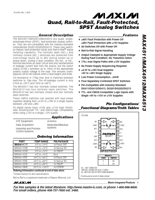
General DescriptionThe MAX4511/MAX4512/MAX4513 are quad, single-pole/single-throw (SPST), fault-protected analog switch-es. They are pin-compatible with the industry-standard nonprotected DG201/DG202/DG213. These new switch-es feature fault-protected inputs and Rail-to-Rail ®signal handling capability. The normally open (NO_) and normally closed (NC_) terminals are protected from overvoltage faults up to 36V during power-up or power-down. During a fault condition, the NO_ or NC_terminal becomes an open circuit and only nanoamperes of leakage current flow from the source, but the switch output (COM_) furnishes up to 10mA of the appropriate polarity supply voltage to the load. This ensures unam-biguous rail-to-rail outputs when a fault begins and ends.On-resistance is 175Ωmax and is matched between switches to 10Ωmax. The off-leakage current is only 0.5nA at +25°C and 10nA at +85°C.The MAX4511 has four normally closed switches. The MAX4512 has four normally open switches. The MAX4513 has two normally closed and two normally open switches.These CMOS switches can operate with dual power supplies ranging from ±4.5V to ±18V or a single supply between +9V and +36V.All digital inputs have +0.8V and +2.4V logic thresh-olds, ensuring both TTL- and CMOS-logic compatibility when using ±15V or a single +12V supply.ApplicationsFeatureso ±40V Fault Protection with Power Off±36V Fault Protection with ±15V Supplies o All Switches Off with Power Off o Rail-to-Rail Signal Handlingo Output Clamped to Appropriate Supply Voltage During Fault Condition; No Transition Glitch o 175Ωmax Signal Paths with ±15V Supplies o No Power-Supply Sequencing Required o ±4.5V to ±18V Dual Supplies +9V to +36V Single Supply o Low Power Consumption, <2mWo Four Separately Controlled SPST Switches o Pin-Compatible with Industry-StandardDG411/DG412/DG413, DG201/DG202/DG213o TTL- and CMOS-Compatible Logic Inputs with Single +9V to +15V or ±15V SuppliesFor free samples & the latest literature: , or phone 1-800-998-8800.For small orders, phone 408-737-7600 ext. 3468.MAX4511/MAX4512/MAX4513Quad, Rail-to-Rail, Fault-Protected,SPST Analog Switches________________________________________________________________Maxim Integrated Products119-4760; Rev 1; 8/02Ordering Information continued at end of data sheet.*Contact factory for dice specifications.Rail-to-Rail is a registered trademark of Nippon Motorola, Ltd.Ordering InformationPin Configurations/Functional Diagrams/Truth TablesATE Equipment Data Acquisition Industrial and Process-Control SystemsAvionicsRedundant/Backup SystemsM A X 4511/M A X 4512/M A X 4513Quad, Rail-to-Rail, Fault-Protected,SPST Analog Switches 2_______________________________________________________________________________________ABSOLUTE MAXIMUM RATINGSELECTRICAL CHARACTERISTICS—Dual Supplies(V+ = +15V, V- = -15V, GND = 0V, T A =T MIN to T MAX , unless otherwise noted. Typical values are at T A = +25°C.)Stresses beyond those listed under “Absolute Maximum Ratings” may cause permanent damage to the device. These are stress ratings only, and functional operation of the device at these or any other conditions beyond those indicated in the operational sections of the specifications is not implied. Exposure to absolute maximum rating conditions for extended periods may affect device reliability.Note 1:COM_ and IN_ pins are not fault protected. Signals on COM_ or IN_ exceeding V+ or V- are clamped by internal diodes.Limit forward diode current to maximum current rating.Note 2:NC_ and NO_ pins are fault protected. Signals on NC_ or NO_ exceeding -36V to +36V may damage the device. Theselimits apply with power applied to V+ or V-, or ±40V with V+ = V- = 0.(Voltages Referenced to GND)V+........................................................................-0.3V to +44.0V V-.........................................................................-44.0V to +0.3V V+ to V-................................................................-0.3V to +44.0V COM_, IN_ (Note 1)..............................(V- - 0.3V) to (V+ + 0.3V)NC_, NO_ (Note 2)..................................(V+ - 36V) to (V- + 36V)NC_, NO_ to COM_.................................................-36V to +36V Continuous Current into Any Terminal..............................±30mA Peak Current into Any Terminal(pulsed at 1ms, 10% duty cycle)...................................±50mAContinuous Power Dissipation (T A = +70°C) (Note 2)Plastic DIP (derate 10.53mW/°C above +70°C)...........842mW Narrow SO (derate 8.70mW/°C above +70°C).............696mW TSSOP (derate 9.4mW/°C above +70°C)..................754.7mW CERDIP (derate 10.00mW/°C above +70°C)................800mW Operating Temperature RangesMAX451_C_ E......................................................0°C to +70°C MAX451_E_ E...................................................-40°C to +85°C MAX451_MJE .................................................-55°C to +125°C Storage Temperature Range.............................-65°C to +150°C Lead Temperature (soldering, 10s).................................+300°CMAX4511/MAX4512/MAX4513Quad, Rail-to-Rail, Fault-Protected,SPST Analog Switches_______________________________________________________________________________________3ELECTRICAL CHARACTERISTICS—Dual Supplies (continued)(V+ = +15V, V- = -15V, GND = 0V, T A =T MIN to T MAX , unless otherwise noted. Typical values are at T A = +25°C.)M A X 4511/M A X 4512/M A X 4513Quad, Rail-to-Rail, Fault-Protected,SPST Analog Switches 4_______________________________________________________________________________________ELECTRICAL CHARACTERISTICS—Dual Supplies (continued)(V+ = +15V, V- = -15V, GND = 0V, T A = T MIN to T MAX , unless otherwise noted. Typical values are at T A = +25°C.)MAX4511/MAX4512/MAX4513Quad, Rail-to-Rail, Fault-Protected,SPST Analog Switches_______________________________________________________________________________________5ELECTRICAL CHARACTERISTICS—Single +12V Supply(V+ = +10.8V to +13.2V, V- = 0, T A = T MIN to T MAX , unless otherwise noted. Typical values are at T A = +25°C.)M A X 4511/M A X 4512/M A X 4513Quad, Rail-to-Rail, Fault-Protected,SPST Analog Switches 6_______________________________________________________________________________________Note 1:COM_ and IN_ pins are not fault protected. Signals on COM_ or IN_ exceeding V+ or V- are clamped by internal diodes.Limit forward diode current to maximum current rating.Note 2:NC_ and NO_ pins are fault protected. Signals on NC_ or NO_ exceeding -36V to +36V may damage the device. These limits apply with power applied to V+ or V-, or ±40V with V+ = V- = 0.Note 3:The algebraic convention is used in this data sheet; the most negative value is shown in the minimum column.Note 4:∆R ON = ∆R ON(MAX)- ∆R ON(MIN).Note 5:Leakage parameters are 100% tested at maximum rated hot temperature and guaranteed by correlation at T A = +25°C.Note 6:Guaranteed by design.Note 7:Off isolation = 20 log10 [ V COM_/ (V NC_or V NO_) ], V COM_= output, V NC_or V NO_= input to off switch.Note 8:Between any two switches.Note 9:Leakage testing for single-supply operation is guaranteed by testing with dual supplies.ELECTRICAL CHARACTERISTICS—Single +12V Supply (continued)(V+ = +10.8V to +13.2V, V- = 0, T A = T MIN to T MAX , unless otherwise noted. Typical values are at T A = +25°C.)MAX4511/MAX4512/MAX4513Quad, Rail-to-Rail, Fault-Protected,SPST Analog Switches_______________________________________________________________________________________7__________________________________________Typical Operating Characteristics(T A = +25°C, unless otherwise noted.)010050250200150300350-20-50-15-105101520SWITCH ON-RESISTANCE vs. V COM (DUAL SUPPLIES)V COM (V)S W I T C H O N -R E S I S T A N C E (Ω)80602040160140100120180200-15-50-1051015SWITCH ON-RESISTANCE vs. V COM AND TEMPERATURE (DUAL SUPPLIES)V COM (V)S W I T C H O N -R E S I S T A N C E (Ω)100010051015202530SWITCH ON-RESISTANCE vs. V COM (SINGLE SUPPLY)V COM (V)S W I T C H O N -R E S I S I T A N C E (Ω)050200150100300350250400046281012SWITCH ON-RESISTANCE vs. V COM AND TEMPERATURE (SINGLE SUPPLY)V COM (V)S W I T C H O N -R E S I S T A N C E (Ω)0300200100700800600500400900100005101520ON AND OFF TIMES vs. SUPPLY VOLTAGESUPPLY VOLTAGE (±V)t O N , t O F F (n s )1p10p100p1n10n 100n-50-25255075100125150I D(ON), I S(OFF), AND I D(OFF) LEAKAGES vs. TEMPERATURETEMPERATURE (°C)L E A K A G E (A )02810641214-15-10-5051015CHARGE INJECTION vs. V COM (DUAL SUPPLIES)V COM (V)Q (p C )010*******500400600-5025-255075100125ON AND OFF TIMES vs. TEMPERATURETEMPERATURE (°C)t O N , t O F F (n s )100300200500400600-50025-255075100125POWER-SUPPLY CURRENT vs. TEMPERATURETEMPERATURE (°C)S U P P L Y C U R R E N T (µA )M A X 4511/M A X 4512/M A X 4513Quad, Rail-to-Rail, Fault-Protected,SPST Analog Switches 8_______________________________________________________________________________________00.51.51.02.52.03.001015520253035LOGIC-LEVEL THRESHOLD vs. V+M A X 4511-10V+ (V)L O G I C -L E V E L T H R E S H O L D (V )Typical Operating Characteristics (continued)(T A = +25°C, unless otherwise noted.)0-10-20-1200.010.11101001000FREQUENCY RESPONSE-90-100-110FREQUENCY (MHz)L O S S (d B )P H A S E (D E G R E E S )-70-80-50-60-30-4012010080-120-60-80-100-20-402006040Pin Description*As long as the voltage on NO_ or NC_ does not exceed V+ or V-, NO_ (or NC_) and COM_ pins are identical and interchange-able. Either may be considered as an input or output; signals pass equally well in either direction.Detailed DescriptionOverview of Traditional Fault-Protected SwitchesThe MAX4511/MAX4512/MAX4513 are fault-protected CMOS analog switches with unusual operation and construction. Traditional fault-protected switches are constructed by three series FETs. This produces good off characteristics, but fairly high on-resistance when the signals are within about 3V of each supply rail. As the voltage on one side of the switch approaches with-in about 3V of either supply rail (a fault condition), the switch impedance becomes higher, limiting the output signal range (on the protected side of the switch) to approximately 3V less than the appropriate polarity supply voltage.During a fault condition, the output current that flows from the protected side of the switch into its load comes from the fault source on the other side of the switch. I f the switch is open or the load is extremely high impedance, the input current will be very low. I f the switch is on and the load is low impedance,enough current will flow from the source to maintain the load voltage at 3V less than the supply.MAX4511/MAX4512/MAX4513Quad, Rail-to-Rail, Fault-Protected,SPST Analog Switches_______________________________________________________________________________________9Overview of MAX4511/MAX4512/MAX4513The MAX4511/MAX4512/MAX4513 differ considerably from traditional fault-protection switches, with several advantages. First, they are constructed with two paral-lel FETs, allowing very low on-resistance when the switch is on. Second, they allow signals on the NC_ or NO_ pins that are within or slightly beyond the supply rails to be passed through the switch to the COM termi-nal, allowing rail-to-rail signal operation. Third, when a signal on NC_ or NO_ exceeds the supply rails by about 50mV (a fault condition), the voltage on COM_ is limited to the appropriate polarity supply voltage.Operation is identical for both fault polarities. The fault-protection extends to ±36V from GND.During a fault condition, the NO_ or NC_ input pin becomes high impedance regardless of the switch state or load resistance. If the switch is on, the COM_output current is furnished from the V+ or V- pin by “booster” FETs connected to each supply pin. These FETs can typically source or sink up to 10mA.When power is removed, the fault protection is still in effect. In this case, the NO_ or NC_ terminals are a vir-tual open circuit. The fault can be up to ±40V.The COM_ pins are not fault protected; they act as nor-mal CMOS switch pins. If a voltage source is connect-ed to any COM_ pin, it should be limited to the supply voltages. Exceeding the supply voltage will cause high currents to flow through the ESD protection diodes,possibly damaging the device (see Absolute Maximum Ratings ).Pin CompatibilityThese switches have identical pinouts to common non-fault-protected CMOS switches. Care should be exer-cised in considering them for direct replacements in existing printed circuit boards, however, since only the NO_ and NC_ pins of each switch are fault protected.Internal ConstructionInternal construction is shown in Figure 1, with the ana-log signal paths shown in bold. A single normally openFigure 1. Block DiagramM A X 4511/M A X 4512/M A X 4513Quad, Rail-to-Rail, Fault-Protected,SPST Analog Switches 10______________________________________________________________________________________(NO) switch is shown; the normally closed (NC) config-uration is identical except the logic-level translator becomes an inverter. The analog switch is formed by the parallel combination of N-channel FET N1 and P-channel FET P1, which are driven on and off simultane-ously according to the input fault condition and the logic-level state.Normal OperationTwo comparators continuously compare the voltage on the NO_ (or NC_) pin with V+ and V-. When the signal on NO_ or NC_ is between V+ and V- the switch acts normally, with FETs N1 and P1 turning on and off in response to I N_ signals. The parallel combination of N1 and P1 forms a low-value resistor between NO_ (or NC_) and COM_ so that signals pass equally well in either direction.Positive Fault ConditionWhen the signal on NO_ (or NC_) exceeds V+ by about 50mV, the high-fault comparator output is high, turning off FETs N1 and P1. This makes the NO_ (or NC_) pin high impedance regardless of the switch state. I f the switch state is “off”, all FETs are turned off and both NO_ (or NC_) and COM_ are high impedance. I f the switch state is “on”, FET P2 is turned on, sourcing cur-rent from V+ to COM_.Negative Fault ConditionWhen the signal on NO_ (or NC_) exceeds V- by about 50mV, the low-fault comparator output is high, turning off FETs N1 and P1. This makes the NO_ (or NC_) pin high impedance regardless of the switch state. I f the switch state is “off,” all FETs are turned off and both NO_ (or NC_) and COM_ are high impedance. I f the switch state is “on,” FET N2 is turned on, sinking cur-rent from COM_ to V-.Transient Fault Response and RecoveryWhen a fast rise-time and fall-time transient on I N_exceeds V+ or V-, the output (COM_) follows the input (I N_) to the supply rail with only a few nanoseconds delay. This delay is due to the switch on-resistance and circuit capacitance to ground. When the input transient returns to within the supply rails, however, there is a longer output recovery time delay. For positive faults, the recovery time is typically 3.5µs. For negative faults, the recovery time is typically 1.3µs. These values depend on the COM_ output resistance and capacitance, and are not production tested or guaranteed. The delays are not dependent on the fault amplitude. Higher COM_ output resistance and capacitance increase recovery times.COM_ and IN_ PinsFETs N2 and P2 can source about ±10mA from V+ or V-to the COM_ pin in the fault condition. Ensure that if the COM_ pin is connected to a low-resistance load, the absolute maximum current rating of 30mA is never exceeded, both in normal and fault conditions.The GND, COM_, and IN_ pins do not have fault protec-tion. Reverse ESD-protection diodes are internally con-nected between GND, COM_, IN_ and both V+ and V-. If a signal on GND, COM_, or I N_ exceeds V+ or V- by more than 300mV, one of these diodes will conduct heavily. During normal operation these reverse-biased ESD diodes leak a few nanoamps of current to V+ and V-.Fault-Protection Voltage and Power OffThe maximum fault voltage on the NC_ or NO_ pins is ±36V with power applied and ±40V with power off.Failure ModesThe MAX4511/MAX4512/MAX4513 are not lightning arrestors or surge protectors.Exceeding the fault-protection voltage limits on NO_ or NC_, even for very short periods, can cause the device to fail. The failure modes may not be obvious, and fail-ure in one switch may or may not affect other switches in the same package.GroundThere is no connection between the analog signal paths and GND. The analog signal paths consist of an N-channel and P-channel MOSFET with their sources and drains paralleled and their gates driven out of phase to V+ and V- by the logic-level translators.V+ and GND power the internal logic and logic-level translators and set the input logic thresholds. The logic-level translators convert the logic levels to switched V+and V- signals to drive the gates of the analog switch-es. This drive signal is the only connection between the power supplies and the analog signals. GND, IN_, and COM_ have ESD-protection diodes to V+ and V-.IN_ Logic-Level ThresholdsThe logic-level thresholds are CMOS and TTL compati-ble when V+ is +15V. As V+ is raised the threshold increases slightly, and when V+ reaches 25V the level threshold is about 2.8V—above the TTL output high level minimum of 2.4V, but still compatible with CMOS outputs (see Typical Operating Characteristics ).Increasing V- has no effect on the logic-level thresholds,but it does increase the gate-drive voltage to the signal FETs, reducing their on-resistance.MAX4511/MAX4512/MAX4513Quad, Rail-to-Rail, Fault-Protected,SPST Analog Switches______________________________________________________________________________________11Bipolar SuppliesThe MAX4511/MAX4512/MAX4513 operate with bipolar supplies between ±4.5V and ±18V. The V+ and V- sup-plies need not be symmetrical, but their difference can not exceed the absolute maximum rating of 44V.Single SupplyThe MAX4511/MAX4512/MAX4513 operate from a sin-gle supply between +9V and +36V when V- is connect-ed to GND.High-Frequency PerformanceIn 50Ωsystems, signal response is reasonably flat up to 50MHz (see Typical Operating Characteristics ). Above20MHz, the on-response has several minor peaks that are highly layout dependent. The problem with high-fre-quency operation is not turning the switch on, but turn-ing it off. The off-state switch acts like a capacitor and passes higher frequencies with less attenuation. At 10MHz, off isolation is about -42dB in 50Ωsystems,becoming worse (approximately 20dB per decade) as frequency increases. Higher circuit impedances also make off isolation worse. Adjacent channel attenuation is about 3dB above that of a bare IC socket and is due entirely to capacitive coupling.Figure 2. Switch Turn-On/Turn-Off TimesTest Circuits/Timing DiagramsFigure 3. MAX4513 Break-Before-Make IntervalM A X 4511/M A X 4512/M A X 4513Quad, Rail-to-Rail, Fault-Protected,SPST Analog Switches 12______________________________________________________________________________________Figure 4. Charge InjectionFigure 5. COM_, NO_, NC_ CapacitanceTest Circuits/Timing Diagrams (continued)MAX4511/MAX4512/MAX4513Quad, Rail-to-Rail, Fault-Protected,SPST Analog Switches______________________________________________________________________________________13Figure 6. Frequency Response, Off Isolation, and CrosstalkTest Circuits/Timing Diagrams (continued)Pin Configurations/Functional Diagrams/Truth Tables (continued)M A X 4511/M A X 4512/M A X 4513Quad, Rail-to-Rail, Fault-Protected,SPST Analog Switches 14______________________________________________________________________________________V-GNDNC4COM4IN4IN3COM30.086"(2.261mm)MAX4511NO1NO2COM1IN1IN2COM2COM4NO4IN4IN3NO3COM30.086"(2.261mm)MAX4512Ordering Information (continued)Chip TopographiesV-GNDCOM4NO4IN4IN3NC3COM3MAX45130.086"(2.261mm)TRANSISTOR COUNT: 139SUBSTRATE CONNECTED TO:V+*Contact factory for dice specifications.MAX4511/MAX4512/MAX4513Quad, Rail-to-Rail, Fault-Protected,SPST Analog Switches______________________________________________________________________________________15Package Information(The package drawing(s) in this data sheet may not reflect the most current specifications. For the latest package outline information,go to /packages .)M A X 4511/M A X 4512/M A X 4513Quad, Rail-to-Rail, Fault-Protected,SPST Analog Switches 16______________________________________________________________________________________Package Information (continued)(The package drawing(s) in this data sheet may not reflect the most current specifications. For the latest package outline information,go to /packages.)MAX4511/MAX4512/MAX4513Quad, Rail-to-Rail, Fault-Protected,SPST Analog SwitchesMaxim cannot assume responsibility for use of any circuitry other than circuitry entirely embodied in a Maxim product. No circuit patent licenses are implied. Maxim reserves the right to change the circuitry and specifications without notice at any time.Maxim Integrated Products, 120 San Gabriel Drive, Sunnyvale, CA 94086 408-737-7600______________________17©2002 Maxim Integrated ProductsPrinted USAis a registered trademark of Maxim Integrated Products.Package Information (continued)(The package drawing(s) in this data sheet may not reflect the most current specifications. For the latest package outline information,go to /packages .)。
MAX2021
零中频I/Q调制器/解调器1.概述MAX2021是一款低噪声、高线性度、直接上变频/下变频、正交调制/解调器,适用于手持RFID、便携式读卡器以及750MHz至1200MHz的单载波/多载波GSM/EDGE、CDMA2000®、WCDMA和iDEN®基站。
与传统的二次变频结构相比,直接变频结构可显著降低发射/接收机成本,减小系统尺寸、降低功耗。
除了高线性度和低噪声优势外,MAX2021还具备很高的集成度。
器件包括:两路匹配的无源混频器用于正交调制/解调、两路LO缓冲放大器和一路LO正交分配器。
另外,芯片还内置非平衡变压器,允许RF和LO单端输入。
作为附加功能,芯片内部还集成了基带输入匹配电路,可直接与发送DAC连接,省去了昂贵的I/Q缓冲放大器。
MAX2021采用单+5V供电,提供结构紧凑的36引脚TQFN (6mm x 6mm)封装,底部带有裸焊盘。
在-40°C至+85°C范围内确保电气特性。
2.关键特性•750MHz至1200MHz RF频率范围•可选择功率模式:通过外部电阻设置器件工作在低功耗/低性能模式•36引脚、(6mm x 6mm)、TQFN封装,提供高隔离度调制器性能:•满足4载波WCDMA的65dBc ACLR要求•OIP3典型值:+21dBm•OIP2典型值:+58dBm•OP1dB典型值:+16.7dBm•LO泄漏典型值:-32dBm•边带抑制典型值:43.5dBc•输出噪声谱密度:-174dBm/Hz•DC至550MHz基带输入可直接与DAC连接,减少了I/Q缓冲器的成本•直流耦合输入允许用户控制失调电压解调器性能:•IIP3典型值:+35.2dBm•IIP2典型值:+76dBm•IP1dB典型值:> 30dBm•转换损耗典型值:9.2dB•NF典型值:9.3dB•I/Q增益平衡:0.06dB•I/Q相位平衡:0.15°3.芯片结构3.1引脚配置/功能框图引脚说明MAX2021是专为在同相(I)和正交(Q)基带的输入在650MHz到1200MHz的RF频率范围中的上变频差。
MAX4172EUA中文资料
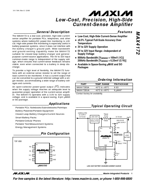
_______________General DescriptionThe MAX4172 is a low-cost, precision, high-side current-sense amplifier for portable PCs, telephones, and other systems where battery/DC power-line monitoring is criti-cal. High-side power-line monitoring is especially useful in battery-powered systems, since it does not interfere with the battery charger’s ground path. Wide bandwidth and ground-sensing capability make the MAX4172 suitable for closed-loop battery-charger and general-purpose current-source applications. The 0V to 32V input common-mode range is independent of the supply volt-age, which ensures that current-sense feedback remains viable, even when connected to a battery in deep dis-charge.To provide a high level of flexibility, the MAX4172 func-tions with an external sense resistor to set the range of load current to be monitored. It has a current output that can be converted to a ground-referred voltage with a sin-gle resistor, accommodating a wide range of battery volt-ages and currents.An open-collector power-good output (PG ) indicates when the supply voltage reaches an adequate level to guarantee proper operation of the current-sense amplifi-er. The MAX4172 operates with a 3.0V to 32V supply voltage, and is available in a space-saving, 8-pin µMAX or SO package.________________________ApplicationsPortable PCs: Notebooks/Subnotebooks/Palmtops Battery-Powered/Portable EquipmentClosed-Loop Battery Chargers/Current Sources Smart-Battery Packs Portable/Cellular PhonesPortable Test/Measurement Systems Energy Management Systems____________________________Featureso Low-Cost, High-Side Current-Sense Amplifier o ±0.5% Typical Full-Scale Accuracy Over Temperature o 3V to 32V Supply Operationo 0V to 32V Input Range—Independent of Supply Voltage o 800kHz Bandwidth [V SENSE = 100mV (1C)]200kHz Bandwidth [V SENSE = 6.25mV (C/16)]o Available in Space-Saving µMAX and SO PackagesMAX4172Low-Cost, Precision, High-SideCurrent-Sense Amplifier________________________________________________________________Maxim Integrated Products 1__________________Pin Configuration__________Typical Operating Circuit19-1184; Rev 0; 12/96For free samples & the latest literature: , or phone 1-800-998-8800*Contact factory for availability.M A X 4172Low-Cost, Precision, High-Side Current-Sense Amplifier 2_______________________________________________________________________________________ABSOLUTE MAXIMUM RATINGSELECTRICAL CHARACTERISTICS(V+ = +3V to +32V; RS+, RS- = 0V to 32V; T A = T MIN to T MAX ; unless otherwise noted. Typical values are at V+ = +12V, RS+ = 12V, T A = +25°C.)Stresses beyond those listed under “Absolute Maximum Ratings” may cause permanent damage to the device. These are stress ratings only, and functional operation of the device at these or any other conditions beyond those indicated in the operational sections of the specifications is not implied. Exposure to absolute maximum rating conditions for extended periods may affect device reliability.V+, RS+, RS-, PG ...................................................-0.3V to +36V OUT..............................................................-0.3V to (V+ + 0.3V)Differential Input Voltage, V RS+- V RS-............................±700mV Current into Any Pin..........................................................±50mA Continuous Power Dissipation (T A = +70°C)SO (derate 5.88mW/°C above +70°C)..........................471mW µMAX (derate 4.10mW/°C above +70°C).....................330mWOperating Temperature RangeMAX4172E_A....................................................-40°C to +85°C Storage Temperature Range.............................-65°C to +150°C Lead Temperature (soldering, 10sec).............................+300°CELECTRICAL CHARACTERISTICS (continued)(V+ = +3V to +32V; RS+, RS- = 0V to 32V; T A = T MIN to T MAX ; unless otherwise noted. Typical values are at V+ = +12V, RS+ = 12V, T A = +25°C.)MAX4172Low-Cost, Precision, High-SideCurrent-Sense Amplifier_______________________________________________________________________________________3100095050010SUPPLY CURRENT vs. SUPPLY VOLTAGE600650550900850800V+ (V)S U P P L Y C U R R E N T (µA )2030750700400.50.4-0.510OUTPUT ERROR vs. SUPPLY VOLTAGE-0.3-0.4-0.20.30.20.1V+ (V)E R R O R (%)20300-0.1401.51.0-3.010C/16 LOAD OUTPUT ERROR vs. SUPPLY VOLTAGE-2.0-1.5-2.50.50V+ (V)E R R O R (%)2030-0.5-1.040__________________________________________Typical Operating Characteristics(V+ = +12V, V RS+= 12V, R OUT = 1k Ω, T A = +25°C, unless otherwise noted.)Note 1:6.25mV = 1/16 of typical full-scale sense voltage (C/16).Note 2:Valid operation of the MAX4172 is guaranteed by design when PG is low.0.750.55-0.6563040OUTPUT ERRORvs. COMMON-MODE VOLTAGE-0.45-0.250.350.15V RS- (V)E R R O R (%)1218-0.05242.952.902.45-40-1585V+ THRESHOLD FOR PG OUTPUT LOWvs. TEMPERATURE2.502.552.602.852.802.752.70TEMPERATURE (°C)V + T R I P T H R E S H O L D (V )10352.656040-50.1m10m 100m1m1ERROR vs. SENSE VOLTAGE0M A X 4172-04V SENSE (V)E R R O R (%)10515202530353500.010.11101001000POWER-SUPPLY REJECTION RATIOvs. FREQUENCY5POWER-SUPPLY FREQUENCY (kHz)E R R O R (%)151020302510µs/div0mV to 10mV V SENSE TRANSIENT RESPONSEGNDV SENSE 5mV/divV OUT 50mV/divGNDMAX4172-0810µs/div0mV to 100mV V SENSE TRANSIENT RESPONSEGNDV SENSE 50mV/divV OUT 500mV/divGNDMAX4172-09M A X 4172Low-Cost, Precision, High-Side Current-Sense Amplifier 4___________________________________________________________________________________________________________________Typical Operating Characteristics (continued)(V+ = +12V, V RS+= 12V, R OUT = 1k Ω, T A = +25°C, unless otherwise noted.)MAX4172Low-Cost, Precision, High-SideCurrent-Sense Amplifier_______________________________________________________________________________________55µs/divSTART-UP DELAYGNDV OUT 500mV/divV+ 2V/divGNDV SENSE = 100mVMAX4172-1010µs/divV+ to PG POWER-UP DELAYGNDPG 2V/divV+ 2V/divGND100k Ω PULL-UP RESISTOR FROM PG TO +4VMAX4172-11______________________________________________________________Pin Description____________________________Typical Operating Characteristics (continued)(V+ = +12V, V RS+= 12V, R OUT = 1k Ω, T A = +25°C, unless otherwise noted.)Current Output. OUT is proportional to the magnitude of the sense voltage (V RS+- V RS-). A 1k Ωresistor from OUT to ground will result in a voltage equal to 10V/V of sense voltage.OUT 6Power Good Open-Collector Logic Output. A low level indicates that V+ is sufficient to power the MAX4172, and adequate time has passed for power-on transients to settle out.PG 7Supply Voltage Input for the MAX4172V+8GroundGND 5No Connect. No internal connection. Leave open or connect to GND.N.C.3, 4PIN Load-side connection for the external sense resistor. The “-” indicates the direction of current flow.RS-2Power connection to the external sense resistor. The “+” indicates the direction of current flow.RS+1FUNCTIONNAME _______________Detailed DescriptionThe MAX4172 is a unidirectional, high-side current-sense amplifier with an input common-mode range that is inde-pendent of supply voltage. This feature not only allows the monitoring of current flow into a battery in deep dis-charge, but also enables high-side current sensing at voltages far in excess of the supply voltage (V+).The MAX4172 current-sense amplifier’s unique topolo-gy simplifies current monitoring and control. The MAX4172’s amplifier operates as shown in Figure 1.The battery/load current flows through the external sense resistor (R SENSE ), from the RS+ node to the RS-node. Current flows through R G1and Q1, and into the current mirror, where it is multiplied by a factor of 50before appearing at OUT.To analyze the circuit of Figure 1, assume that current flows from RS+ to RS-, and that OUT is connected to GND through a resistor. Since A1’s inverting input is high impedance, no current flows though R G2(neglect-ing the input bias current), so A1’s negative input is equal to V SOURCE - (I LOAD x R SENSE ). A1’s open-loop gain forces its positive input to essentially the same voltage level as the negative input. Therefore, the drop across R G1equals I LOAD x R SENSE . Then, since I RG1M A X 4172flows through R G1, I RG1x R G1= I LOAD x R SENSE . The internal current mirror multiplies I RG1by a factor of 50to give I OUT = 50 x I RG1. Substituting I OUT / 50 for I RG1,(I OUT / 50) x R G1 = I LOAD x R SENSE , or:I OUT = 50 x I LOAD x (R SENSE / R G1)The internal current gain of 50 and the factory-trimmed resistor R G1combine to result in the MAX4172transconductance (G m ) of 10mA/V. G m is de-fined as being equal to I OUT / (V RS+- V RS-). Since (V RS+- V RS-) = I LOAD x R SENSE , the output current (I OUT ) can be calculated with the following formula:I OUT = G m x (V RS+- V RS-) =(10mA/V) x (I LOAD x R SENSE )Current OutputThe output voltage equation for the MAX4172 is given below:V OUT = (G m ) x (R SENSE x R OUT x I LOAD )where V OUT = the desired full-scale output voltage,I LOAD = the full-scale current being sensed, R SENSE =the current-sense resistor, R OUT = the voltage-setting resistor, and G m = MAX4172 transconductance (10mA/V).The full-scale output voltage range can be set by changing the R OUT resistor value, but the output volt-age must be no greater than V+ - 1.2V. The above equation can be modified to determine the R OUT required for a particular full-scale range:R OUT = (V OUT ) / (I LOAD x R SENSE x G m )OUT is a high-impedance current source that can be integrated by connecting it to a capacitive load.PG OutputThe PG output is an open-collector logic output that indicates the status of the MAX4172’s V+ power sup-ply. A logic low on the PG output indicates that V+ is sufficient to power the MAX4172. This level is tempera-ture dependent (see Typical Operating Characteristics graphs), and is typically 2.7V at room temperature. The internal PG comparator has a 100mV (typical) hystere-sis to prevent possible oscillations caused by repeated toggling of the PG output, making the device ideal for power-management systems lacking soft-start capabili-ty. An internal delay (15µs typical) in the PG compara-tor allows adequate time for power-on transients to settle out. The PG status indicator greatly simplifies the design of closed-loop systems by ensuring that the components in the control loop have sufficient voltage to operate correctly.__________Applications InformationSuggested Component Valuesfor Various ApplicationsThe Typical Operating Circuit is useful in a wide variety of applications. Table 1 shows suggested component values and indicates the resulting scale factors for vari-ous applications required to sense currents from 100mA to 10A.Adjust the R SENSE value to monitor higher or lower cur-rent levels. Select R SENSE using the guidelines and for-mulas in the following section.Sense Resistor, R SENSEChoose R SENSE based on the following criteria:•Voltage Loss:A high R SENSE value causes thepower-source voltage to degrade through IR loss.For minimal voltage loss, use the lowest R SENSE value.Low-Cost, Precision, High-Side Current-Sense Amplifier6_______________________________________________________________________________________Figure 1. Functional Diagram•Accuracy:A high R SENSE value allows lower cur-rents to be measured more accurately. This is because offsets become less significant when the sense voltage is larger. For best performance,select R SENSE to provide approximately 100mV of sense voltage for the full-scale current in each application.•Efficiency and Power Dissipation:At high currentlevels, the I 2R losses in R SENSE can be significant.Take this into consideration when choosing the resistor value and its power dissipation (wattage)rating. Also, the sense resistor’s value might drift if it is allowed to heat up excessively.•Inductance:Keep inductance low if I SENSE has a large high-frequency component. Wire-wound resis-tors have the highest inductance, while metal film is somewhat better. Low-inductance metal-film resis-tors are also available. Instead of being spiral wrapped around a core, as in metal-film or wire-wound resistors, they are a straight band of metal and are available in values under 1Ω.•Cost:If the cost of R SENSE is an issue, you mightwant to use an alternative solution, as shown in Figure 2. This solution uses the PC board traces to create a sense resistor. Because of the inaccura-cies of the copper resistor, the full-scale current value must be adjusted with a potentiometer. Also,copper’s resistance temperature coefficient is fairly high (approximately 0.4%/°C).In Figure 2, assume that the load current to be mea-sured is 10A, and that you have determined a 0.3-inch-wide, 2-ounce copper to be appropriate. The resistivity of 0.1-inch-wide, 2-ounce (70µm thickness) copper is 30m Ω/ft. For 10A, you might want R SENSE = 5m Ωfor a 50mV drop at full scale. This resistor requires about 2inches of 0.1-inch-wide copper trace.Current-Sense Adjustment (Resistor Range, Output Adjust)Choose R OUT after selecting R SENSE . Choose R OUT to obtain the full-scale voltage you require, given the full-scale I OUT determined by R SENSE . OUT’s high imped-ance permits using R OUT values up to 200k Ωwith minimal error. OUT’s load impedance (e.g., the input of an op amp or ADC) must be much greater than R OUT (e.g., 100 x R OUT ) to avoid degrading measurement accuracy.High-Current MeasurementThe MAX4172 can achieve high-current measurements by using low-value sense resistors, which can be paral-leled to further increase the current-sense limit. As an alternative, PC board traces can be adjusted over a wide range.MAX4172Low-Cost, Precision, High-SideCurrent-Sense Amplifier_______________________________________________________________________________________7Table 1. Suggested Component ValuesFigure 2. MAX4172 Connections Showing Use of PC BoardMaxim cannot assume responsibility for use of any circuitry other than circuitry entirely embodied in a Maxim product. No circuit patent licenses are implied. Maxim reserves the right to change the circuitry and specifications without notice at any time.8___________________Maxim Integrated Products, 120 San Gabriel Drive, Sunnyvale, CA 94086 (408) 737-7600©1996 Maxim Integrated ProductsPrinted USAis a registered trademark of Maxim Integrated Products.M A X 4172Low-Cost, Precision, High-Side Current-Sense Amplifier ___________________Chip Information________________________________________________________Package InformationPower-Supply Bypassing and GroundingIn most applications, grounding the MAX4172 requires no special precautions. However, in high-current sys-tems, large voltage drops can develop across the ground plane, which can add to or subtract from V OUT .Use a single-point star ground for the highest current-measurement accuracy.The MAX4172 requires no special bypassing and responds quickly to transient changes in line current. If the noise at OUT caused by these transients is a prob-lem, you can place a 1µF capacitor at the OUT pin to ground. You can also place a large capacitor at the RS terminal (or load side of the MAX4172) to decouple the load, reducing the current transients. These capacitors are not required for MAX4172 operation or stability. The RS+ and RS- inputs can be filtered by placing a capac-itor (e.g., 1µF) between them to average the sensed current.TRANSISTOR COUNT: 177SUBSTRATE CONNECTED TO GND。
MAX487ESA中文资料
For pricing, delivery, and ordering information,please contact Maxim/Dallas Direct!at 1-888-629-4642, or visit Maxim’s website at .General DescriptionThe MAX481, MAX483, MAX485, MAX487–MAX491, and MAX1487 are low-power transceivers for RS-485 and RS-422 communication. Each part contains one driver and one receiver. The MAX483, MAX487, MAX488, and MAX489feature reduced slew-rate drivers that minimize EMI and reduce reflections caused by improperly terminated cables,thus allowing error-free data transmission up to 250kbps.The driver slew rates of the MAX481, MAX485, MAX490,MAX491, and MAX1487 are not limited, allowing them to transmit up to 2.5Mbps.These transceivers draw between 120µA and 500µA of supply current when unloaded or fully loaded with disabled drivers. Additionally, the MAX481, MAX483, and MAX487have a low-current shutdown mode in which they consume only 0.1µA. All parts operate from a single 5V supply.Drivers are short-circuit current limited and are protected against excessive power dissipation by thermal shutdown circuitry that places the driver outputs into a high-imped-ance state. The receiver input has a fail-safe feature that guarantees a logic-high output if the input is open circuit.The MAX487 and MAX1487 feature quarter-unit-load receiver input impedance, allowing up to 128 MAX487/MAX1487 transceivers on the bus. Full-duplex communi-cations are obtained using the MAX488–MAX491, while the MAX481, MAX483, MAX485, MAX487, and MAX1487are designed for half-duplex applications.________________________ApplicationsLow-Power RS-485 Transceivers Low-Power RS-422 Transceivers Level TranslatorsTransceivers for EMI-Sensitive Applications Industrial-Control Local Area Networks__Next Generation Device Features♦For Fault-Tolerant ApplicationsMAX3430: ±80V Fault-Protected, Fail-Safe, 1/4Unit Load, +3.3V, RS-485 TransceiverMAX3440E–MAX3444E: ±15kV ESD-Protected,±60V Fault-Protected, 10Mbps, Fail-Safe, RS-485/J1708 Transceivers♦For Space-Constrained ApplicationsMAX3460–MAX3464: +5V, Fail-Safe, 20Mbps,Profibus RS-485/RS-422 TransceiversMAX3362: +3.3V, High-Speed, RS-485/RS-422Transceiver in a SOT23 PackageMAX3280E–MAX3284E: ±15kV ESD-Protected,52Mbps, +3V to +5.5V, SOT23, RS-485/RS-422,True Fail-Safe ReceiversMAX3293/MAX3294/MAX3295: 20Mbps, +3.3V,SOT23, RS-855/RS-422 Transmitters ♦For Multiple Transceiver ApplicationsMAX3030E–MAX3033E: ±15kV ESD-Protected,+3.3V, Quad RS-422 Transmitters ♦For Fail-Safe ApplicationsMAX3080–MAX3089: Fail-Safe, High-Speed (10Mbps), Slew-Rate-Limited RS-485/RS-422Transceivers♦For Low-Voltage ApplicationsMAX3483E/MAX3485E/MAX3486E/MAX3488E/MAX3490E/MAX3491E: +3.3V Powered, ±15kV ESD-Protected, 12Mbps, Slew-Rate-Limited,True RS-485/RS-422 TransceiversMAX481/MAX483/MAX485/MAX487–MAX491/MAX1487Low-Power, Slew-Rate-Limited RS-485/RS-422 Transceivers______________________________________________________________Selection Table19-0122; Rev 8; 10/03Ordering Information appears at end of data sheet.M A X 481/M A X 483/M A X 485/M A X 487–M A X 491/M A X 1487Low-Power, Slew-Rate-Limited RS-485/RS-422 Transceivers 2_______________________________________________________________________________________ABSOLUTE MAXIMUM RATINGSSupply Voltage (V CC ).............................................................12V Control Input Voltage (RE , DE)...................-0.5V to (V CC + 0.5V)Driver Input Voltage (DI).............................-0.5V to (V CC + 0.5V)Driver Output Voltage (A, B)...................................-8V to +12.5V Receiver Input Voltage (A, B).................................-8V to +12.5V Receiver Output Voltage (RO).....................-0.5V to (V CC +0.5V)Continuous Power Dissipation (T A = +70°C)8-Pin Plastic DIP (derate 9.09mW/°C above +70°C)....727mW 14-Pin Plastic DIP (derate 10.00mW/°C above +70°C)..800mW 8-Pin SO (derate 5.88mW/°C above +70°C).................471mW14-Pin SO (derate 8.33mW/°C above +70°C)...............667mW 8-Pin µMAX (derate 4.1mW/°C above +70°C)..............830mW 8-Pin CERDIP (derate 8.00mW/°C above +70°C).........640mW 14-Pin CERDIP (derate 9.09mW/°C above +70°C).......727mW Operating Temperature RangesMAX4_ _C_ _/MAX1487C_ A...............................0°C to +70°C MAX4__E_ _/MAX1487E_ A.............................-40°C to +85°C MAX4__MJ_/MAX1487MJA...........................-55°C to +125°C Storage Temperature Range.............................-65°C to +160°C Lead Temperature (soldering, 10sec).............................+300°CDC ELECTRICAL CHARACTERISTICS(V CC = 5V ±5%, T A = T MIN to T MAX , unless otherwise noted.) (Notes 1, 2)Stresses beyond those listed under “Absolute Maximum Ratings” may cause permanent damage to the device. These are stress ratings only, and functional operation of the device at these or any other conditions beyond those indicated in the operational sections of the specifications is not implied. Exposure to absolute maximum rating conditions for extended periods may affect device reliability.V V IN = -7VV IN = 12V V IN = -7V V IN = 12V Input Current (A, B)I IN2V TH k Ω48-7V ≤V CM ≤12V, MAX487/MAX1487R INReceiver Input Resistance -7V ≤V CM ≤12V, all devices except MAX487/MAX1487R = 27Ω(RS-485), Figure 40.4V ≤V O ≤2.4VR = 50Ω(RS-422)I O = 4mA, V ID = -200mV I O = -4mA, V ID = 200mV V CM = 0V-7V ≤V CM ≤12V DE, DI, RE DE, DI, RE MAX487/MAX1487,DE = 0V, V CC = 0V or 5.25VDE, DI, RE R = 27Ωor 50Ω, Figure 4R = 27Ωor 50Ω, Figure 4R = 27Ωor 50Ω, Figure 4DE = 0V;V CC = 0V or 5.25V,all devices except MAX487/MAX1487CONDITIONSk Ω12µA ±1I OZRThree-State (high impedance)Output Current at ReceiverV 0.4V OL Receiver Output Low Voltage 3.5V OH Receiver Output High Voltage mV 70∆V TH Receiver Input Hysteresis V -0.20.2Receiver Differential Threshold Voltage-0.2mA 0.25mA-0.81.01.55V OD2Differential Driver Output (with load)V 2V 5V OD1Differential Driver Output (no load)µA±2I IN1Input CurrentV 0.8V IL Input Low Voltage V 2.0V IH Input High Voltage V 0.2∆V OD Change in Magnitude of Driver Common-Mode Output Voltage for Complementary Output States V 0.2∆V OD Change in Magnitude of Driver Differential Output Voltage for Complementary Output States V 3V OC Driver Common-Mode Output VoltageUNITS MINTYPMAX SYMBOL PARAMETERMAX481/MAX483/MAX485/MAX487–MAX491/MAX1487Low-Power, Slew-Rate-Limited RS-485/RS-422 Transceivers_______________________________________________________________________________________3SWITCHING CHARACTERISTICS—MAX481/MAX485, MAX490/MAX491, MAX1487(V CC = 5V ±5%, T A = T MIN to T MAX , unless otherwise noted.) (Notes 1, 2)DC ELECTRICAL CHARACTERISTICS (continued)(V CC = 5V ±5%, T A = T MIN to T MAX , unless otherwise noted.) (Notes 1, 2)ns 103060t PHLDriver Rise or Fall Time Figures 6 and 8, R DIFF = 54Ω, C L1= C L2= 100pF ns MAX490M, MAX491M MAX490C/E, MAX491C/E2090150MAX481, MAX485, MAX1487MAX490M, MAX491MMAX490C/E, MAX491C/E MAX481, MAX485, MAX1487Figures 6 and 8, R DIFF = 54Ω,C L1= C L2= 100pF MAX481 (Note 5)Figures 5 and 11, C RL = 15pF, S2 closedFigures 5 and 11, C RL = 15pF, S1 closed Figures 5 and 11, C RL = 15pF, S2 closed Figures 5 and 11, C RL = 15pF, S1 closed Figures 6 and 10, R DIFF = 54Ω,C L1= C L2= 100pFFigures 6 and 8,R DIFF = 54Ω,C L1= C L2= 100pF Figures 6 and 10,R DIFF = 54Ω,C L1= C L2= 100pF CONDITIONS ns 510t SKEW ns50200600t SHDNTime to ShutdownMbps 2.5f MAX Maximum Data Rate ns 2050t HZ Receiver Disable Time from High ns 103060t PLH 2050t LZ Receiver Disable Time from Low ns 2050t ZH Driver Input to Output Receiver Enable to Output High ns 2050t ZL Receiver Enable to Output Low 2090200ns ns 134070t HZ t SKD Driver Disable Time from High |t PLH - t PHL |DifferentialReceiver Skewns 4070t LZ Driver Disable Time from Low ns 4070t ZL Driver Enable to Output Low 31540ns51525ns 31540t R , t F 2090200Driver Output Skew to Output t PLH , t PHL Receiver Input to Output4070t ZH Driver Enable to Output High UNITS MIN TYP MAX SYMBOL PARAMETERFigures 7 and 9, C L = 100pF, S2 closed Figures 7 and 9, C L = 100pF, S1 closed Figures 7 and 9, C L = 15pF, S1 closed Figures 7 and 9, C L = 15pF, S2 closedM A X 481/M A X 483/M A X 485/M A X 487–M A X 491/M A X 1487Low-Power, Slew-Rate-Limited RS-485/RS-422 Transceivers 4_______________________________________________________________________________________SWITCHING CHARACTERISTICS—MAX483, MAX487/MAX488/MAX489(V CC = 5V ±5%, T A = T MIN to T MAX , unless otherwise noted.) (Notes 1, 2)SWITCHING CHARACTERISTICS—MAX481/MAX485, MAX490/MAX491, MAX1487 (continued)(V CC = 5V ±5%, T A = T MIN to T MAX , unless otherwise noted.) (Notes 1, 2)3001000Figures 7 and 9, C L = 100pF, S2 closed Figures 7 and 9, C L = 100pF, S1 closed Figures 5 and 11, C L = 15pF, S2 closed,A - B = 2VCONDITIONSns 40100t ZH(SHDN)Driver Enable from Shutdown toOutput High (MAX481)nsFigures 5 and 11, C L = 15pF, S1 closed,B - A = 2Vt ZL(SHDN)Receiver Enable from Shutdownto Output Low (MAX481)ns 40100t ZL(SHDN)Driver Enable from Shutdown toOutput Low (MAX481)ns 3001000t ZH(SHDN)Receiver Enable from Shutdownto Output High (MAX481)UNITS MINTYP MAX SYMBOLPARAMETERt PLH t SKEW Figures 6 and 8, R DIFF = 54Ω,C L1= C L2= 100pFt PHL Figures 6 and 8, R DIFF = 54Ω,C L1= C L2= 100pFDriver Input to Output Driver Output Skew to Output ns 100800ns ns 2000MAX483/MAX487, Figures 7 and 9,C L = 100pF, S2 closedt ZH(SHDN)Driver Enable from Shutdown to Output High2502000ns2500MAX483/MAX487, Figures 5 and 11,C L = 15pF, S1 closedt ZL(SHDN)Receiver Enable from Shutdown to Output Lowns 2500MAX483/MAX487, Figures 5 and 11,C L = 15pF, S2 closedt ZH(SHDN)Receiver Enable from Shutdown to Output Highns 2000MAX483/MAX487, Figures 7 and 9,C L = 100pF, S1 closedt ZL(SHDN)Driver Enable from Shutdown to Output Lowns 50200600MAX483/MAX487 (Note 5) t SHDN Time to Shutdownt PHL t PLH , t PHL < 50% of data period Figures 5 and 11, C RL = 15pF, S2 closed Figures 5 and 11, C RL = 15pF, S1 closed Figures 5 and 11, C RL = 15pF, S2 closed Figures 5 and 11, C RL = 15pF, S1 closed Figures 7 and 9, C L = 15pF, S2 closed Figures 6 and 10, R DIFF = 54Ω,C L1= C L2= 100pFFigures 7 and 9, C L = 15pF, S1 closed Figures 7 and 9, C L = 100pF, S1 closed Figures 7 and 9, C L = 100pF, S2 closed CONDITIONSkbps 250f MAX 2508002000Maximum Data Rate ns 2050t HZ Receiver Disable Time from High ns 25080020002050t LZ Receiver Disable Time from Low ns 2050t ZH Receiver Enable to Output High ns 2050t ZL Receiver Enable to Output Low ns ns 1003003000t HZ t SKD Driver Disable Time from High I t PLH - t PHL I DifferentialReceiver SkewFigures 6 and 10, R DIFF = 54Ω,C L1= C L2= 100pFns 3003000t LZ Driver Disable Time from Low ns 2502000t ZL Driver Enable to Output Low ns Figures 6 and 8, R DIFF = 54Ω,C L1= C L2= 100pFns 2502000t R , t F 2502000Driver Rise or Fall Time ns t PLH Receiver Input to Output2502000t ZH Driver Enable to Output High UNITS MIN TYP MAX SYMBOL PARAMETERMAX481/MAX483/MAX485/MAX487–MAX491/MAX1487Low-Power, Slew-Rate-Limited RS-485/RS-422 Transceivers_______________________________________________________________________________________530002.5OUTPUT CURRENT vs.RECEIVER OUTPUT LOW VOLTAGE525M A X 481-01OUTPUT LOW VOLTAGE (V)O U T P U T C U R R E N T (m A )1.515100.51.02.0203540450.90.1-50-252575RECEIVER OUTPUT LOW VOLTAGE vs.TEMPERATURE0.30.7TEMPERATURE (°C)O U T P U TL O W V O L T A G E (V )500.50.80.20.60.40100125-20-41.5 2.0 3.0 5.0OUTPUT CURRENT vs.RECEIVER OUTPUT HIGH VOLTAGE-8-16M A X 481-02OUTPUT HIGH VOLTAGE (V)O U T P U T C U R R E N T (m A )2.5 4.0-12-18-6-14-10-203.54.5 4.83.2-50-252575RECEIVER OUTPUT HIGH VOLTAGE vs.TEMPERATURE3.64.4TEMPERATURE (°C)O U T P UT H I G H V O L T A G E (V )0504.04.63.44.23.83.01001259000 1.0 3.0 4.5DRIVER OUTPUT CURRENT vs.DIFFERENTIAL OUTPUT VOLTAGE1070M A X 481-05DIFFERENTIAL OUTPUT VOLTAGE (V)O U T P U T C U R R E N T (m A )2.0 4.05030806040200.5 1.5 2.53.5 2.31.5-50-2525125DRIVER DIFFERENTIAL OUTPUT VOLTAGEvs. TEMPERATURE1.72.1TEMPERATURE (°C)D I F FE R E N T I A L O U T P U T V O L T A G E (V )751.92.21.62.01.8100502.4__________________________________________Typical Operating Characteristics(V CC = 5V, T A = +25°C, unless otherwise noted.)NOTES FOR ELECTRICAL/SWITCHING CHARACTERISTICSNote 1:All currents into device pins are positive; all currents out of device pins are negative. All voltages are referenced to deviceground unless otherwise specified.Note 2:All typical specifications are given for V CC = 5V and T A = +25°C.Note 3:Supply current specification is valid for loaded transmitters when DE = 0V.Note 4:Applies to peak current. See Typical Operating Characteristics.Note 5:The MAX481/MAX483/MAX487 are put into shutdown by bringing RE high and DE low. If the inputs are in this state for lessthan 50ns, the parts are guaranteed not to enter shutdown. If the inputs are in this state for at least 600ns, the parts are guaranteed to have entered shutdown. See Low-Power Shutdown Mode section.M A X 481/M A X 483/M A X 485/M A X 487–M A X 491/M A X 1487Low-Power, Slew-Rate-Limited RS-485/RS-422 Transceivers 6___________________________________________________________________________________________________________________Typical Operating Characteristics (continued)(V CC = 5V, T A = +25°C, unless otherwise noted.)120008OUTPUT CURRENT vs.DRIVER OUTPUT LOW VOLTAGE20100M A X 481-07OUTPUT LOW VOLTAGE (V)O U T P U T C U R R E N T (m A )6604024801012140-1200-7-5-15OUTPUT CURRENT vs.DRIVER OUTPUT HIGH VOLTAGE-20-80M A X 481-08OUTPUT HIGH VOLTAGE (V)O U T P U T C U R R E N T (m A )-31-603-6-4-2024-100-40100-40-60-2040100120MAX1487SUPPLY CURRENT vs. TEMPERATURE300TEMPERATURE (°C)S U P P L Y C U R R E N T (µA )20608050020060040000140100-50-2550100MAX481/MAX485/MAX490/MAX491SUPPLY CURRENT vs. TEMPERATURE300TEMPERATURE (°C)S U P P L Y C U R R E N T (µA )257550020060040000125100-50-2550100MAX483/MAX487–MAX489SUPPLY CURRENT vs. TEMPERATURE300TEMPERATURE (°C)S U P P L Y C U R R E N T (µA )257550020060040000125MAX481/MAX483/MAX485/MAX487–MAX491/MAX1487Low-Power, Slew-Rate-Limited RS-485/RS-422 Transceivers_______________________________________________________________________________________7______________________________________________________________Pin DescriptionFigure 1. MAX481/MAX483/MAX485/MAX487/MAX1487 Pin Configuration and Typical Operating CircuitM A X 481/M A X 483/M A X 485/M A X 487–M A X 491/M A X 1487__________Applications InformationThe MAX481/MAX483/MAX485/MAX487–MAX491 and MAX1487 are low-power transceivers for RS-485 and RS-422 communications. The MAX481, MAX485, MAX490,MAX491, and MAX1487 can transmit and receive at data rates up to 2.5Mbps, while the MAX483, MAX487,MAX488, and MAX489 are specified for data rates up to 250kbps. The MAX488–MAX491 are full-duplex trans-ceivers while the MAX481, MAX483, MAX485, MAX487,and MAX1487 are half-duplex. In addition, Driver Enable (DE) and Receiver Enable (RE) pins are included on the MAX481, MAX483, MAX485, MAX487, MAX489,MAX491, and MAX1487. When disabled, the driver and receiver outputs are high impedance.MAX487/MAX1487:128 Transceivers on the BusThe 48k Ω, 1/4-unit-load receiver input impedance of the MAX487 and MAX1487 allows up to 128 transceivers on a bus, compared to the 1-unit load (12k Ωinput impedance) of standard RS-485 drivers (32 trans-ceivers maximum). Any combination of MAX487/MAX1487 and other RS-485 transceivers with a total of 32 unit loads or less can be put on the bus. The MAX481/MAX483/MAX485 and MAX488–MAX491 have standard 12k ΩReceiver Input impedance.Low-Power, Slew-Rate-Limited RS-485/RS-422 Transceivers 8_______________________________________________________________________________________Figure 2. MAX488/MAX490 Pin Configuration and Typical Operating CircuitFigure 3. MAX489/MAX491 Pin Configuration and Typical Operating CircuitMAX483/MAX487/MAX488/MAX489:Reduced EMI and ReflectionsThe MAX483 and MAX487–MAX489 are slew-rate limit-ed, minimizing EMI and reducing reflections caused by improperly terminated cables. Figure 12 shows the dri-ver output waveform and its Fourier analysis of a 150kHz signal transmitted by a MAX481, MAX485,MAX490, MAX491, or MAX1487. High-frequency har-monics with large amplitudes are evident. Figure 13shows the same information displayed for a MAX483,MAX487, MAX488, or MAX489 transmitting under the same conditions. Figure 13’s high-frequency harmonics have much lower amplitudes, and the potential for EMI is significantly reduced.MAX481/MAX483/MAX485/MAX487–MAX491/MAX1487Low-Power, Slew-Rate-Limited RS-485/RS-422 Transceivers_______________________________________________________________________________________9_________________________________________________________________Test CircuitsFigure 4. Driver DC Test Load Figure 5. Receiver Timing Test LoadFigure 6. Driver/Receiver Timing Test Circuit Figure 7. Driver Timing Test LoadM A X 481/M A X 483/M A X 485/M A X 487–M A X 491/M A X 1487Low-Power, Slew-Rate-Limited RS-485/RS-422 Transceivers 10_______________________________________________________Switching Waveforms_________________Function Tables (MAX481/MAX483/MAX485/MAX487/MAX1487)Figure 8. Driver Propagation DelaysFigure 9. Driver Enable and Disable Times (except MAX488 and MAX490)Figure 10. Receiver Propagation DelaysFigure 11. Receiver Enable and Disable Times (except MAX488and MAX490)Table 1. TransmittingTable 2. ReceivingLow-Power Shutdown Mode (MAX481/MAX483/MAX487)A low-power shutdown mode is initiated by bringing both RE high and DE low. The devices will not shut down unless both the driver and receiver are disabled.In shutdown, the devices typically draw only 0.1µA of supply current.RE and DE may be driven simultaneously; the parts are guaranteed not to enter shutdown if RE is high and DE is low for less than 50ns. If the inputs are in this state for at least 600ns, the parts are guaranteed to enter shutdown.For the MAX481, MAX483, and MAX487, the t ZH and t ZL enable times assume the part was not in the low-power shutdown state (the MAX485/MAX488–MAX491and MAX1487 can not be shut down). The t ZH(SHDN)and t ZL(SHDN)enable times assume the parts were shut down (see Electrical Characteristics ).It takes the drivers and receivers longer to become enabled from the low-power shutdown state (t ZH(SHDN ), t ZL(SHDN)) than from the operating mode (t ZH , t ZL ). (The parts are in operating mode if the –R —E –,DE inputs equal a logical 0,1 or 1,1 or 0, 0.)Driver Output ProtectionExcessive output current and power dissipation caused by faults or by bus contention are prevented by two mechanisms. A foldback current limit on the output stage provides immediate protection against short cir-cuits over the whole common-mode voltage range (see Typical Operating Characteristics ). In addition, a ther-mal shutdown circuit forces the driver outputs into a high-impedance state if the die temperature rises excessively.Propagation DelayMany digital encoding schemes depend on the differ-ence between the driver and receiver propagation delay times. Typical propagation delays are shown in Figures 15–18 using Figure 14’s test circuit.The difference in receiver delay times, | t PLH - t PHL |, is typically under 13ns for the MAX481, MAX485,MAX490, MAX491, and MAX1487 and is typically less than 100ns for the MAX483 and MAX487–MAX489.The driver skew times are typically 5ns (10ns max) for the MAX481, MAX485, MAX490, MAX491, and MAX1487, and are typically 100ns (800ns max) for the MAX483 and MAX487–MAX489.MAX481/MAX483/MAX485/MAX487–MAX491/MAX1487Low-Power, Slew-Rate-Limited RS-485/RS-422 Transceivers______________________________________________________________________________________1110dB/div0Hz5MHz500kHz/div10dB/div0Hz5MHz500kHz/divFigure 12. Driver Output Waveform and FFT Plot of MAX481/MAX485/MAX490/MAX491/MAX1487 Transmitting a 150kHz SignalFigure 13. Driver Output Waveform and FFT Plot of MAX483/MAX487–MAX489 Transmitting a 150kHz SignalM A X 481/M A X 483/M A X 485/M A X 487–M A X 491/M A X 1487Low-Power, Slew-Rate-Limited RS-485/RS-422 Transceivers 12______________________________________________________________________________________V CC = 5V T A = +25°CV CC = 5V T A = +25°CV CC = 5V T A = +25°CV CC = 5V T A = +25°CFigure 14. Receiver Propagation Delay Test CircuitFigure 15. MAX481/MAX485/MAX490/MAX491/MAX1487Receiver t PHLFigure 16. MAX481/MAX485/MAX490/MAX491/MAX1487Receiver t PLHPHL Figure 18. MAX483, MAX487–MAX489 Receiver t PLHLine Length vs. Data RateThe RS-485/RS-422 standard covers line lengths up to 4000 feet. For line lengths greater than 4000 feet, see Figure 23.Figures 19 and 20 show the system differential voltage for the parts driving 4000 feet of 26AWG twisted-pair wire at 110kHz into 120Ωloads.Typical ApplicationsThe MAX481, MAX483, MAX485, MAX487–MAX491, and MAX1487 transceivers are designed for bidirectional data communications on multipoint bus transmission lines.Figures 21 and 22 show typical network applications circuits. These parts can also be used as line repeaters, with cable lengths longer than 4000 feet, as shown in Figure 23.To minimize reflections, the line should be terminated at both ends in its characteristic impedance, and stub lengths off the main line should be kept as short as possi-ble. The slew-rate-limited MAX483 and MAX487–MAX489are more tolerant of imperfect termination.MAX481/MAX483/MAX485/MAX487–MAX491/MAX1487Low-Power, Slew-Rate-Limited RS-485/RS-422 Transceivers______________________________________________________________________________________13DIV Y -V ZRO5V 0V1V0V -1V5V 0V2µs/divFigure 19. MAX481/MAX485/MAX490/MAX491/MAX1487 System Differential Voltage at 110kHz Driving 4000ft of Cable Figure 20. MAX483, MAX487–MAX489 System Differential Voltage at 110kHz Driving 4000ft of CableFigure 21. MAX481/MAX483/MAX485/MAX487/MAX1487 Typical Half-Duplex RS-485 NetworkM A X 481/M A X 483/M A X 485/M A X 487–M A X 491/M A X 1487Low-Power, Slew-Rate-Limited RS-485/RS-422 Transceivers 14______________________________________________________________________________________Figure 22. MAX488–MAX491 Full-Duplex RS-485 NetworkFigure 23. Line Repeater for MAX488–MAX491Isolated RS-485For isolated RS-485 applications, see the MAX253 and MAX1480 data sheets.MAX481/MAX483/MAX485/MAX487–MAX491/MAX1487Low-Power, Slew-Rate-Limited RS-485/RS-422 Transceivers______________________________________________________________________________________15_______________Ordering Information_________________Chip TopographiesMAX481/MAX483/MAX485/MAX487/MAX1487N.C. RO 0.054"(1.372mm)0.080"(2.032mm)DE DIGND B N.C.V CCARE * Contact factory for dice specifications.__Ordering Information (continued)M A X 481/M A X 483/M A X 485/M A X 487–M A X 491/M A X 1487Low-Power, Slew-Rate-Limited RS-485/RS-422 Transceivers 16______________________________________________________________________________________TRANSISTOR COUNT: 248SUBSTRATE CONNECTED TO GNDMAX488/MAX490B RO 0.054"(1.372mm)0.080"(2.032mm)N.C. DIGND Z A V CCYN.C._____________________________________________Chip Topographies (continued)MAX489/MAX491B RO 0.054"(1.372mm)0.080"(2.032mm)DE DIGND Z A V CCYREMAX481/MAX483/MAX485/MAX487–MAX491/MAX1487Low-Power, Slew-Rate-Limited RS-485/RS-422 Transceivers______________________________________________________________________________________17Package Information(The package drawing(s) in this data sheet may not reflect the most current specifications. For the latest package outline information go to /packages .)S O I C N .E P SM A X 481/M A X 483/M A X 485/M A X 487–M A X 491/M A X 1487Low-Power, Slew-Rate-Limited RS-485/RS-422 Transceivers 18______________________________________________________________________________________Package Information (continued)(The package drawing(s) in this data sheet may not reflect the most current specifications. For the latest package outline information go to /packages .)MAX481/MAX483/MAX485/MAX487–MAX491Low-Power, Slew-Rate-Limited RS-485/RS-422 TransceiversMaxim cannot assume responsibility for use of any circuitry other than circuitry entirely embodied in a Maxim product. No circuit patent licenses are implied. Maxim reserves the right to change the circuitry and specifications without notice at any time.Maxim Integrated Products, 120 San Gabriel Drive, Sunnyvale, CA 94086 408-737-7600 ____________________19©2003 Maxim Integrated ProductsPrinted USAis a registered trademark of Maxim Integrated Products.M A X 481/M A X 483/M A X 485/M A X 487–M A X 491/M A X 1487P D I P N .E PSPackage Information (continued)(The package drawing(s) in this data sheet may not reflect the most current specifications. For the latest package outline information go to /packages .)。
MAX4040ESA+中文资料

________________________Applications
Battery-Powered Systems Portable/Battery-Powered Electronic Equipment Digital Scales Strain Gauges Sensor Amplifiers Cellular Phones Notebook Computers PDAs
____________________________Features
♦ Single-Supply Operation Down to +2.4V ♦ Ultra-Low Power Consumption: 10µA Supply Current per Amplifier 1µA Shutdown Mode (MAX4041/MAX4043) ♦ Rail-to-Rail Input Common-Mode Range ♦ Outputs Swing Rail-to-Rail ♦ No Phase Reversal for Overdriven Inputs ♦ 200µV Input Offset Voltage ♦ Unity-Gain Stable for Capacitive Loads up to 200pF ♦ 90kHz Gain-Bandwidth Product ♦ Available in Space-Saving 5-Pin SOT23 and 8-Pin µMAX® Packages
元器件交易网
Single/Dual/Quad, Low-Cost, SOT23, Micropower, Rail-to-Rail I/O Op Amps MAX4040–MAX4044
ABSOLUTE MAXIMUM RATINGS
MAX21100中文资料

%
-0.05 ±0.008 +0.05 %/°C
-6
±0.5
+6
dps
-0.15 ±0.025 +0.15 dps/°C
0.45
deg/√hr
Bias Stability
GBSTAB
4
deg/hr
Nonlinearity at +25°C (Note 5)
Low-Noise Mode Eco Mode, GODR = 250Hz
User selectable
MIN TYP MAX
±250 ±500 ±1000 ±2000 0.009 0.018
0.025
2
2000
UNITS
dps
dps/ √Hz Hz
Highpass Cutoff Frequency (Low-Noise Mode)
MAX21100
低功耗、超高精度6+3自由度的 惯性测量单元DoF IMU
Absolute Maximum Ratings
VDD........................................................................-0.3V to +6.0V VDDIO....................................................................-0.3V to +6.0V REGD....................................... -0.3V to min (VDD + 0.3V,+2.2V) INT1, INT2, SDA_SDI_O, SA0_SDO, SCL_CLK, CS, DSYNC,
MAX3222EEUP中文资料
Battery-Powered Equipment Cell Phones Cell-Phone Data Cables Notebook, Subnotebook, and Palmtop Computers
Applications
Printers Smart Phones xDSL Modems
_______________Ordering Information
PART
TEMP RANGE
PINPACKAGE
PKG CODE
MAX3222ECTP MAX3222ECUP
0°C to +70°C 0°C to +70°C
20 Thin QFNEP** (5mm x 5mm) 20 TSSOP
♦ For Low-Voltage or Data Cable Applications MAX3380E/MAX3381E: +2.35V to +5.5V, 1µA, 2Tx/2Rx, RS-232 Transceivers with ±15kV ESD-Protected I/O and Logic Pins
MAX3222EEPN -40°C to +85°C 18 Plastic DIP —
MAX3232ECAE 0°C to +70°C 16 SSOP
—
MAX3232ECWE 0°C to +70°C 16 Wide SO —
MAX3232ECPE 0°C to +70°C 16 Plastic DIP —
A proprietary low-dropout transmitter output stage delivers true RS-232 performance from a +3.0V to +5.5V power supply, using an internal dual charge pump. The charge pump requires only four small 0.1µF capacitors for operation from a +3.3V supply. Each device guarantees operation at data rates of 250kbps while maintaining RS-232 output levels. The MAX3237E guarantees operation at 250kbps in the normal operating mode and 1Mbps in the MegaBaud™ operating mode, while maintaining RS-232compliant output levels.
MAX5222中文资料完整

令中。
Figure 图 3.详细的串行接口时序图
数字输入 数字输入与 CMOS 逻辑兼容。当通过 0.3 ✕ VDD 和 0.7 ✕ VDD 之间的过渡区切换逻辑 输入时,电源电流稍微增加。 微处理器接口 MAX5222 串行接口与 Microwire、SPI 和 QSPI 兼容。对于 SPI,清除 CPOL 和 CPHA 位 (CPOL=0 和 CPHA=0)。cpol=0 将非活动时 钟状态设置为零,CPHA=0 更改 SCLK 下降沿 的数据。此设置允许 SPI 以全时钟速度运行。 如果您的祄 P 上没有串行端口,则可以使用 并行端口的 3 位逐位模拟串行端口操作。只 有在必要时才操作串行时钟,从而使电压输 出处的数字馈通最小化。
工作温度范围…………-40°C 至+85°C
接 地 的 所 有 其 他 插 脚 ( 注 1 ) -0.3V 至 结温…………………………………+150°C
(VDD+0.3V)
储存温度范围……………………-65°C 至
持续功耗(Ta=+70°C)
+150°C
8 针 SOT23(在+70°C 以上减额 8.7mW/° 铅温度(焊接 10s)……………………………
CIN
Note4
10
pF
动态性能
电压输出滑移速率 电压输出稳定时间 数字馈通 和串扰
电源电压范围 电源电流
关机电源电流
SR
CL = 100pF
1
To ± 1⁄2LSB, CL = 100pF
10
All 0s to all 1s
0.25
电源
VDD
2.7
5.5
ALL INPUTS=0 IDD
MAX5432_07中文资料

Operating Temperature Range ...........................-40°C to +85°C Junction Temperature ......................................................+150°C Storage Temperature Range .............................-60°C to +150°C Lead Temperature (soldering, 10s) .................................+300°C
The MAX5432–MAX5435 feature an internal, nonvolatile, electrically erasable programmable read-only memory (EEPROM) that returns the wiper to its previously stored position at power-up. The fast-mode I2C-compatible serial interface allows communication at data rates up to 400kbps, minimizing board space and reducing interconnection complexity. Each device is available with multiple factory-preset I2C addresses (see the Ordering Information/Selector Guide).
MAX232中文资料(官方版)
新一代 器件特性 ____________________________
♦ 对于低电压、集成 ESD 保护的应用 MAX3222E/MAX3232E/MAX3237E/MAX3241E/ MAX3246E:+3.0V 至 +5.5V、低功耗、速率高达 1Mbps、利用四个 0.1µF 电容实现真正的 RS-232 收发器 (MAX3246E 提供 UCSPTM 封装 )。 ♦ 对于低成本应用 MAX221E:±15kV ESD 保护、+5V、1µA、 具有 AutoShutdownTM 功能的单芯片 RS-232。
________________________________ 应用
便携式计算机 低功耗调制解调器 接口转换 电池供电 RS-232 系统 多点 RS-232 网络
_____________________________ 定购信息
PART MAX220CPE MAX220CSE MAX220CWE MAX220C/D MAX220EPE MAX220ESE MAX220EWE MAX220EJE MAX220MJE TEMP RANGE 0°C to +70°C 0°C to +70°C 0°C to +70°C 0°C to +70°C -40°C to +85°C -40°C to +85°C -40°C to +85°C -40°C to +85°C -55°C to +125°C PIN-PACKAGE 16 Plastic DIP 16 Narrow SO 16 Wide SO Dice* 16 Plastic DIP 16 Narrow SO 16 Wide SO 16 CERDIP 16 CERDIP
MAX412CSA+,MAX412ESA+,MAX410ESA+,MAX412CPA+,MAX412EPA+,MAX414CSD+,MAX410BCSA, 规格书,Datasheet 资料

Applications
Low-Noise Frequency Synthesizers Infrared Detectors High-Quality Audio Amplifiers Ultra Low-Noise Instrumentation Amplifiers Bridge Signal Conditioning
ELECTRICAL CHARACTERISTICS
(V+ = 5V, V- = -5V, TA = +25°C, unless otherwise noted.)
PARAMETER Input Offset Voltage Input Bias Current Input Offset Current Differential Input Resistance Common-Mode Input Resistance Input Capacitance SYMBOL VOS IB IOS RIN(Diff) RIN(CM) CIN MAX410, MAX412, MAX414 Input Noise-Voltage Density en MAX410B, MAX412B, MAX414B fO = 10Hz fO = 1000Hz ±3.5 VCM = ±3.5V VS = ±2.4V to ±5.25V RL = 2kΩ, VO = ±3.6V RL = 600Ω, VO = ±3.5V RL = 2kΩ 115 96 115 110 +3.6 -3.7 10Hz 1000Hz (Note 2) 1000Hz (Note 2) CONDITIONS MAX410, MAX410B, MAX412, MAX412B MAX414, MAX414B MIN TYP ±120 ±150 ±80 ±40 20 40 4 7 1.5 2.4 2.6 1.2 +3.7/ -3.8 130 103 122 120 +3.7/ -3.8 35 10kΩ || 20pF load 10kΩ || 20pF load To 0.1% fO = 1kHz 4.5 28 1.3 135 2.4 4.0 pA√Hz V dB dB dB V mA V/µs MHz µs dB nV√Hz MAX ±250 ±320 ±150 ±80 UNITS µV nA nA kΩ MΩ pF
MAX4252EUA中文资料
— — ACCI AEYJ
Ordering Information continued at end of data sheet. Selector Guide appears at end of data sheet.
Pin Configurations
TOP VIEW (BUMPS ON BOTTOM)
5-Pin SOT23 (derate 7.1mW/°C above +70°C)...........571mW 8-Bump UCSP (derate 4.7mW/°C above +70°C)........379mW 8-Pin µMAX (derate 4.5mW/°C above +70°C) ............362mW 8-Pin SO (derate 5.88mW/°C above +70°C)...............471mW 10-Bump UCSP (derate 6.1mW/°C above +70°C) ......484mW
Note 1:
This device is constructed using a unique set of packaging techniques that impose a limit on the thermal profile the device can be exposed to during board-level solder attach and rework. This limit permits only the use of the solder profiles recommended in the industry-standard specification, JEDEC 020A, paragraph 7.6, Table 3 for IR/VPR and Convection Reflow. Preheating is required. Hand or wave soldering is not allowed.
MAX4211AEUE+中文资料
19-3285; Rev 1; 5/05
KITS ATION EVALU ABLE AVAIL
High-Side Power and Current Monitors
General Description Features
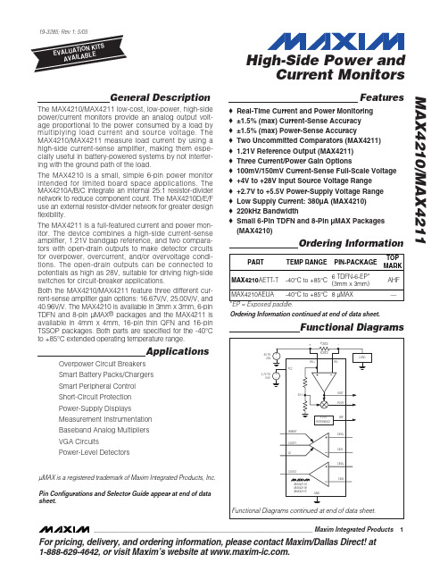
o o o o o o o o o o o o Real-Time Current and Power Monitoring ±1.5% (max) Current-Sense Accuracy ±1.5% (max) Power-Sense Accuracy Two Uncommitted Comparators (MAX4211) 1.21V Reference Output (MAX4211) Three Current/Power Gain Options 100mV/150mV Current-Sense Full-Scale Voltage +4V to +28V Input Source Voltage Range +2.7V to +5.5V Power-Supply Voltage Range Low Supply Current: 380µA (MAX4210) 220kHz Bandwidth Small 6-Pin TDFN and 8-Pin µMAX Packages (MAX4210)
4V TO 28V
+ -
+ -
25:1
IOUT POUT
1.21V REFERENCE INHIBIT
REF
CIN1+
COUT1 CIN1LE CIN2+ COUT2
µMAX is a registered trademark of Maxim Integrated Products, Inc. Pin Configurations and Selector Guide appear at end of data sheet.
MAX1241中文资料datasheet

MAX1240 / MAX1241 采用 8 引脚封装的低 功耗、12 位模数转换器转换器(ADC)。 MAX1240 采 用 + 2.7V 至 + 3.6V 的 电 源 供 电,MAX1241 采用单电源供电范围是+ 2.7V 至+ 5.25V。这两款设备都具有 7.5μs 的功 能 逐次逼近 ADC,快速跟踪/保持(1.5μs), 片上时钟和高速 3 线串行接口。 在 73ksps 的 最 大 采 样 速 度 下 , 功 耗 仅 为 37mW(VDD = 3V)。2μA 关断模式以较 慢的吞吐率来降低功耗。 MAX1240 具 有 内 部 2.5V 参 考 电 压 , 而 MAX1241 需要外部参考电 压。MAX1241 接受从 0V 到VREF 和参考信号输入范围包括 正电源轨。外部的时钟从 3 线接口访问数据, 它直接连接到标准微控制器的 I/O 港口。该 接口与 SPI™,QSPI™和 MICROWIRE™兼容。 该接卓越的交流特性和极低的功耗,易于使 用和小封装尺寸,使这些转换器成为远程传 感器和数据采集应用的理想之选,或者是要 求降低功耗和对空间有要求的电路的最好 选择。MAX1240/MAX1241 采用 8 引脚 PDIP 和 SO 封装。
兑换率
转换时间 跟踪/保持采集时 间 转换时间 吞吐率 光圈抖动
tCONV
t ACQ
t APR
fSCLK=2.1MHz 图8
5.5
7.5
us
1.5
us
73
ksps
30
ns
<50
ps
模拟输入
输入电压范围 输入电容
0
VREF V
16
pF
电源要求
MAX4232中文资料

General DescriptionThe MAX4230–MAX4234 single/dual/quad, high-output-drive CMOS op amps feature 200mA of peak output current, rail-to-rail input, and output capability from a single 2.7V to 5.5V supply. These amplifiers exhibit a high slew rate of 10V/µs and a gain-bandwidth product (GBWP) of 10MHz. The MAX4230–MAX4234 can drive typical headset levels (32Ω), as well as bias an RF power amplifier (PA) in wireless handset applications.The MAX4230 comes in a tiny 5-pin SC70 package and the MAX4231, single with shutdown, is offered in the 6-pin SC70 package. The dual op-amp MAX4233 is offered in the space-saving 10-bump UCSP™, provid-ing the smallest footprint area for a dual op amp with shutdown.These op amps are designed to be part of the PA con-trol circuitry, biasing RF PAs in wireless headsets. The MAX4231/MAX4233 offer a SHDN feature that drives the output low. This ensures that the RF PA is fully dis-abled when needed, preventing unconverted signals to the RF antenna.The MAX4230 family offers low offsets, wide bandwidth,and high-output drive in a tiny 2.1mm x 2.0mm space-saving SC70 package. These parts are offered over the automotive temperature range (-40°C to +125°C).ApplicationsRF PA Biasing Controls in Handset Applications Portable/Battery-Powered Audio Applications Portable Headphone Speaker Drivers (32Ω)Audio Hands-Free Car Phones (Kits)Laptop/Notebook Computers/TFT Panels Sound Ports/Cards Set-Top BoxesDigital-to-Analog Converter Buffers Transformer/Line Drivers Motor DriversFeatureso 30mA Output Drive Capability o Rail-to-Rail Input and Output o 1.1mA Supply Current per Amplifier o 2.7V to 5.5V Single-Supply Operation o 10MHz Gain-Bandwidth Product o High Slew Rate: 10V/µso 100dB Voltage Gain (R L = 100k Ω)o 85dB Power-Supply Rejection Ratio o No Phase Reversal for Overdriven Inputs o Unity-Gain Stable for Capacitive Loads to 780pF o Low-Power Shutdown Mode Reduces Supply Current to <1µA o Available in 5-Pin SC70 Package (MAX4230)o Available in 10-Bump UCSP Package (MAX4233)MAX4230–MAX4234High-Output-Drive, 10MHz, 10V/µs,Rail-to-Rail I/O Op Amps with Shutdown in SC70________________________________________________________________Maxim Integrated Products 119-2164; Rev 4; 5/04Ordering Information continued at end of data sheet.For pricing, delivery, and ordering information,please contact Maxim/Dallas Direct!at 1-888-629-4642, or visit Maxim’s website at .Selector Guide appears at end of data sheet.Pin Configurations appear at end of data sheet.UCSP is a trademark of Maxim Integrated Products, Inc.Ordering InformationTypical Operating CircuitM A X 4230–M A X 4234High-Output-Drive, 10MHz, 10V/µs,Rail-to-Rail I/O Op Amps with Shutdown in SC702_______________________________________________________________________________________ABSOLUTE MAXIMUM RATINGSStresses beyond those listed under “Absolute Maximum Ratings” may cause permanent damage to the device. These are stress ratings only, and functional operation of the device at these or any other conditions beyond those indicated in the operational sections of the specifications is not implied. Exposure to absolute maximum rating conditions for extended periods may affect device reliability.Supply Voltage (V DD to V SS )....................................................6V All Other Pins....................................(V SS - 0.3V) + (V DD + 0.3V)Output Short-Circuit Duration to V DD or V SS (Note 1)..................1s Continuous Power Dissipation (T A = +70°C)5-Pin SC70 (derate 3.1mW/°C above +70°C)..............247mW 5-Pin SOT23 (derate 7.1mW/°C above +70°C)............571mW 6-Pin SC70 (derate 3.1mW/°C above +70°C)..............245mW 6-Pin SOT23 (derate 8.7mW/°C above +70°C) ...........696mW 8-Pin SOT23 (derate 8.9mW/°C above +70°C) ...........714mW 8-Pin µMAX (derate 4.5mW/°C above +70°C) ............362mW 10-Pin µMAX (derate 5.6mW/°C above +70°C) ..........444mW 10-Bump UCSP (derate 6.1mW/°C above +70°C) .....484mW 14-Pin TSSOP (derate 9.1mW/°C above +70°C) ........727mW 14-Pin SO (derate 8.3mW/°C above +70°C) ...............667mW Operating Temperature Range .........................-40°C to +125°C Junction Temperature......................................................+150°C Storage Temperature Range.............................-65°C to +150°C Lead Temperature (soldering, 10s).................................+300°CNote 1:Package power dissipation should also be observed.DC ELECTRICAL CHARACTERISTICS(V DD = 2.7V, V SS = 0V, V CM = V DD /2, V OUT = (V DD /2), R L = ∞connected to (V DD /2), V SHDN = V DD , T A = +25°C , unless otherwiseMAX4230–MAX4234High-Output-Drive, 10MHz, 10V/µs,Rail-to-Rail I/O Op Amps with Shutdown in SC70_______________________________________________________________________________________3DC ELECTRICAL CHARACTERISTICS (continued)(V DD = 2.7V, V SS = 0V, V CM = V DD /2, V OUT = (V DD /2), R L = ∞connected to (V DD /2), V SHDN = V DD , T A = +25°C , unless otherwise noted.) (Note 2)DC ELECTRICAL CHARACTERISTICS(V DD = 2.7V, V SS = 0V, V CM = V DD /2, V OUT = (V DD /2), R L = ∞connected to (V DD /2), V SHDN = V DD , T A = -40 to +125°C , unless oth-M A X 4230–M A X 4234High-Output-Drive, 10MHz, 10V/µs,Rail-to-Rail I/O Op Amps with Shutdown in SC704_______________________________________________________________________________________Note 3:SHDN logic parameters are for MAX4231/MAX4233 only.DC ELECTRICAL CHARACTERISTICS (continued)(V DD = 2.7V, V SS = 0V, V CM = V DD /2, V OUT = (V DD /2), R L = ∞connected to (V DD /2), V SHDN = V DD , T A = -40 to +125°C , unless oth-erwise noted.) (Note 2)AC ELECTRICAL CHARACTERISTICS(V DD = 2.7V, V SS = 0V, V CM = V DD /2, V OUT = (V DD /2), R L = ∞connected to (V DD /2), V SHDN = V DD , T A = +25°C , unless otherwise noted.)(Note 2)MAX4230–MAX4234High-Output-Drive, 10MHz, 10V/µs,Rail-to-Rail I/O Op Amps with Shutdown in SC70_______________________________________________________________________________________5GAIN AND PHASE vs. FREQUENCYFREQUENCY (Hz)0.01k 10k100k1M10M 0.1k 1k100MG A I N (d B )70-30-20-100102030605040P H A S E (D E G R E E S )120-90-60-300906030GAIN AND PHASE vs. FREQUENCY(C L = 250pF)FREQUENCY (Hz)0.01k 10k100k1M10M 0.1k 1k100MG A I N (d B )70-30-20-100102030605040-180P H A S E(D E G R E E S )120-150-120-90-60-30090603000.40.20.80.61.21.01.41.81.62.0-4002040-206080100120SUPPLY CURRENT vs. TEMPERATUREM A X 4230 t o c 05TEMPERATURE (°C)S U P P L Y C U R R E N T (m A )POWER-SUPPLY REJECTION RATIOvs. FREQUENCYFREQUENCY (Hz)0.01k10k100k1M0.1k1k10MP S R R (d B )0-100-90-80-70-60-50-40-10-20-3010001001010.10.011k100k 1M10k10MOUTPUT IMPEDANCE vs. FREQUENCYFREQUENCY (Hz)O U T P U T I M P E D A N C E (Ω)5060708090100110-400-2020406080100120TEMPERATURE (°C)S U P P L Y C U R R E N T (n A )SUPPLY CURRENT vs. TEMPERATURE(SHDN = LOW)__________________________________________Typical Operating Characteristics(V DD = 2.7V, V SS = 0V, V CM = V DD /2, V OUT = V DD /2, R L = ∞, connected to V DD /2, V SHDN = V DD , T A = +25°C, unless otherwise noted.)M A X 4230–M A X 4234High-Output-Drive, 10MHz, 10V/µs,Rail-to-Rail I/O Op Amps with Shutdown in SC706_______________________________________________________________________________________00.60.40.21.00.81.81.61.41.22.02.02.53.03.54.04.55.05.5M A X 4230 t o c 07SUPPLY VOLTAGE (V)S U P P L Y C U R R E N T (m A )SUPPLY CURRENT PER AMPLIFIERvs. SUPPLY VOLTAGE-40-2020406080100120TEMPERATURE (°C)-2-1012V O S (m V )INPUT OFFSET VOLTAGE vs. TEMPERATURE020406080100-400-2020406080100120OUTPUT SWING HIGH vs. TEMPERATURETEMPERATURE (°C)V D D - V O U T (m V )040208060120100140-40020-20406080100120OUTPUT SWING LOW vs. TEMPERATURETEMPERATURE (°C)V O U T - V S S (m V )0.20.80.60.41.01.21.402.01.50.5 1.0 2.53.0 3.54.0 4.55.0SUPPLY CURRENT PER AMPLIFIER vs. COMMON-MODE VOLTAGECOMMON-MODE VOLTAGE (V)S U P P L Y C U R R E N T (m A )-2.0-1.0-1.5-0.50.501.000.51.01.52.02.5INPUT OFFSET VOLTAGE vs. COMMON-MODE VOLTAGEM A X 4230/3 t o c 11COMMON-MODE VOLTAGE (V)I N P U T O F F S E T V O L T A G E (m V )0.20.60.41.00.81.20.51.01.52.02.5SUPPLY CURRENT PER AMPLIFIER vs. COMMON-MODE VOLTAGECOMMON-MODE VOLTAGE (V)S U P P L Y C U R R E N T (m A )0.45101001k10k100kTOTAL HARMONIC DISTORTION PLUS NOISE vs. FREQUENCY0.05FREQUENCY (Hz)T H D +N (%)0.150.250.350.300.200.1000.40TOTAL HARMONIC DISTORTION PLUS NOISE vs. PEAK-TO-PEAK OUTPUT VOLTAGEPEAK-TO-PEAK (V)T H D +N (%)100.00014.04.24.65.00.0010.11 4.44.8____________________________Typical Operating Characteristics (continued)(V DD = 2.7V, V SS = 0V, V CM = V DD /2, V OUT = V DD /2, R L = ∞, connected to V DD /2, V SHDN = V DD , T A = +25°C, unless otherwise noted.)MAX4230–MAX4234High-Output-Drive, 10MHz, 10V/µs,Rail-to-Rail I/O Op Amps with Shutdown in SC70_______________________________________________________________________________________7400ns/div SMALL-SIGNAL TRANSIENT RESPONSE (NONINVERTING)IN50mV/divMAX4230/34 toc16OUT400ns/div SMALL-SIGNAL TRANSIENT RESPONSE (INVERTING)IN50mV/divMAX4230/34 toc17OUT400ns/divLARGE-SIGNAL TRANSIENT RESPONSE (NONINVERTING)IN1V/div MAX4230/34 toc18OUT400ns/divLARGE-SIGNAL TRANSIENT RESPONSE (INVERTING)IN1V/divMAX4230/34 toc19OUT0501501002002502.03.02.53.54.04.55.0OUTPUT CURRENT vs. OUTPUT VOLTAGE(SOURCING, V DD = 5.0V)OUTPUT VOLTAGE (V)O U T P U T C U R R E N T (m A )20103060705040801.0 1.4 1.6 1.82.01.2 2.2 2.4 2.6 2.83.0OUTPUT CURRENT vs. OUTPUT VOLTAGE(SOURCING, V DD = 2.7V)OUTPUT VOLTAGE (V)O U T P U T C U R R E N T (m A )-80-60-70-40-50-30-20-10000.40.60.20.8 1.0 1.2 1.4 1.6OUTPUT CURRENT vs. OUTPUT VOLTAGE(SINKING, V DD = 2.7V)OUTPUT VOLTAGE (V)O U T P U T C U R R E N T (m A )-250-200-100-150-5001.00.51.52.02.53.0OUTPUT CURRENT vs. OUTPUT VOLTAGE(SINKING, V DD= 5.0V)OUTPUT VOLTAGE (V)O U T P U T C U R R E N T (m A )2001001010010k 100kFREQUENCY (Hz)I N P U T V O L T A G E N O I S E (n V /√H z )1k INPUT VOLTAGE NOISE vs. FREQUENCYM A X 4230/34 t o c 24____________________________Typical Operating Characteristics (continued)(V DD = 2.7V, V SS = 0V, V CM = V DD /2, V OUT = V DD /2, R L = ∞, connected to V DD /2, V SHDN = V DD , T A = +25°C, unless otherwise noted.)M A X 4230–M A X 4234Detailed DescriptionRail-to-Rail Input StageThe MAX4230–MAX4234 CMOS operational amplifiers have parallel-connected N- and P-channel differential input stages that combine to accept a common-mode range extending to both supply rails. The N-channel stage is active for common-mode input voltages typi-cally greater than (V SS + 1.2V), and the P-channel stage is active for common-mode input voltages typi-cally less than (V DD - 1.2V).Applications InformationPackage Power DissipationWarning: Due to the high output current drive, this op amp can exceed the absolute maximum power-dissi-pation rating.As a general rule, as long as the peak cur-rent is less than or equal to 40mA, the maximum packagepower dissipation is not exceeded for any of the package types offered. There are some exceptions to this rule,however. The absolute maximum power-dissipation rating of each package should always be verified using the fol-lowing equations. The equation below gives an approxi-mation of the package power dissipation:where:V RMS = RMS voltage from V DD to V OUT when sourcing current and RMS voltage from V OUT to V SS when sink-ing current.I RMS = RMS current flowing out of or into the op amp and the load.θ= phase difference between the voltage and the cur-rent. For resistive loads, COS θ= 1.P V I COS IC DISS RMS RMS ()≅θHigh-Output-Drive, 10MHz, 10V/µs,Rail-to-Rail I/O Op Amps with Shutdown in SC708_______________________________________________________________________________________For example, the circuit in Figure 1 has a package power dissipation of 196mW:where:V DC= the DC component of the output voltage.I DC= the DC component of the output current.V PEAK= the highest positive excursion of the AC com-ponent of the output voltage.I PEAK= the highest positive excursion of the AC com-ponent of the output current.Therefore:P IC(DISS)= V RMS I RMS COS θ= 196mWAdding a coupling capacitor improves the package power dissipation because there is no DC current to the load, as shown in Figure 2:Therefore:P IC(DISS)= V RMS I RMS COS θ= 15.6mWIf the configuration in Figure 1 were used with all four of the MAX4234 amplifiers, the absolute maximum power-dissipation rating of this package would be exceeded (see the Absolute Maximum Ratings section).60mW Single-Supply StereoHeadphone Driver Two MAX4230/MAX4231s can be used as a single-sup-ply, stereo headphone driver. The circuit shown in Figure 2 can deliver 60mW per channel with 1% distor-tion from a single 5V supply.The input capacitor (C IN), in conjunction with R IN, forms a highpass filter that removes the DC bias from the incoming signal. The -3dB point of the highpass filter isgiven by:MAX4230–MAX4234High-Output-Drive, 10MHz, 10V/µs, Rail-to-Rail I/O Op Amps with Shutdown in SC70_______________________________________________________________________________________9Figure 2. Circuit Example: Adding a Coupling CapacitorGreatly Reduces Power Dissipation of its PackageFigure 1. MAX4230/MAX4231 Used in Single-Supply OperationCircuit ExampleM A X 4230–M A X 4234Choose gain-setting resistors R IN and R F according to the amount of desired gain, keeping in mind the maxi-mum output amplitude. The output coupling capacitor,C OUT , blocks the DC component of the amplifier out-put, preventing DC current flowing to the load. The out-put capacitor and the load impedance form a highpass filer with the -3dB point determined by:For a 32Ωload, a 100µF aluminum electrolytic capaci-tor gives a low-frequency pole at 50Hz.Bridge AmplifierThe circuit shown in Figure 3 uses a dual MAX4230 to implement a 3V, 200mW amplifier suitable for use in size-constrained applications. This configuration elimi-nates the need for the large coupling capacitor required by the single op-amp speaker driver when sin-gle-supply operation is necessary. Voltage gain is set to 10V/V; however, it can be changed by adjusting the 82k Ωresistor value.Rail-to-Rail Input StageThe MAX4230–MAX4234 CMOS op amps have parallel-connected N- and P-channel differential input stages that combine to accept a common-mode range extend-ing to both supply rails. The N-channel stage is active for common-mode input voltages typically greater than (V SS + 1.2V), and the P-channel stage is active for common-mode input voltages typically less than (V DD -1.2V).Rail-to-Rail Output StageThe minimum output is within millivolts of ground for sin-gle-supply operation, where the load is referenced to ground (V SS ). Figure 4 shows the input voltage range and the output voltage swing of a MAX4230 connected as a voltage follower. The maximum output voltage swing is load dependent; however, it is guaranteed to be within 500mV of the positive rail (V DD = 2.7V) even with maximum load (32Ωto ground).The MAX4230–MAX4234 incorporate a smart short-cir-cuit protection feature. When V OUT is shorted to V DD or V SS , the device detects a fault condition and limits the output current, therefore protecting the device and the application circuit. If V OUT is shorted to any voltage other than V DD or V SS , the smart short-circuit protection is not activated. When the smart short circuit is not active, the output currents can exceed 200mA (see Typical Operating Characteristics .)Input CapacitanceOne consequence of the parallel-connected differential input stages for rail-to-rail operation is a relatively large input capacitance C IN (5pF typ). This introduces a pole at frequency (2πR ′C IN )-1, where R ′is the parallel combi-nation of the gain-setting resistors for the inverting or noninverting amplifier configuration (Figure 5). If the pole frequency is less than or comparable to the unity-gain bandwidth (10MHz), the phase margin is reduced, and the amplifier exhibits degraded AC performance through either ringing in the step response or sustained oscilla-tions. The pole frequency is 10MHz when R ′= 2k Ω. To maximize stability, R ′<< 2k Ωis recommended.High-Output-Drive, 10MHz, 10V/µs,Rail-to-Rail I/O Op Amps with Shutdown in SC7010______________________________________________________________________________________Figure 4. Rail-to-Rail Input/Output RangeFigure 3. Dual MAX4230/MAX4231 Bridge Amplifier for 200mW at 3VIN (1V/div)OUT (1V/div)5µs/divV CC = 3.0V R L = 100k ΩTo improve step response when R ′> 2k Ω, connect small capacitor C f between the inverting input and out-put. Choose C f as follows:C f = 8(R / R f ) [pf] where R f is the feedback resistor and R is the gain-set-ting resistor (Figure 5).Driving Capacitive LoadsThe MAX4230–MAX4234 have a high tolerance for capacitive loads. They are stable with capacitive loads up to 780pF. Figure 6 is a graph of the stable operating region for various capacitive loads vs. resistive loads.Figures 7 and 8 show the transient response with excessive capacitive loads (1500pF), with and without the addition of an isolation resistor in series with the output. Figure 9 shows a typical noninverting capaci-tive-load-driving circuit in the unity-gain configuration.MAX4230–MAX4234Rail-to-Rail I/O Op Amps with Shutdown in SC70______________________________________________________________________________________11Figure 5. Inverting and Noninverting Amplifiers with Feedback CompensationFigure 6. Capacitive-Load Stability1µs/divV DD = 3.0V, C L = 1500pF R L = 100k Ω, R ISO = 39ΩFigure 8. Small-Signal Transient Response with Excessive Capacitive Load with Isolation Resistor1µs/divV DD = 3.0V, C L = 1500pF R L = 100k Ω, R ISO = 0ΩFigure 7. Small-Signal Transient Response with Excessive Capacitive LoadM A X 4230–M A X 4234The resistor improves the circuit ’s phase margin by iso-lating the load capacitor from the op amp ’s output.Power-Up and Shutdown ModesThe MAX4231/MAX4233 have a shutdown option.When the shutdown pin (SHDN ) is pulled low, supply current drops to 0.5µA per amplifier (V DD = 2.7V), the amplifiers are disabled, and their outputs are driven to V SS . Since the outputs are actively driven to V SS in shutdown, any pullup resistor on the output causes a current drain from the supply. Pulling SHDN high enables the amplifier. In the dual MAX4233, the two amplifiers shut down independently. Figure 10 shows the MAX4231’s output voltage to a shutdown pulse. The MAX4231–MAX4234 typically settle within 5µs after power-up. Figures 11 and 12 show I DD to a shutdown plus and voltage power-up cycle.When exiting shutdown, there is a 6µs delay before the amplifier ’s output becomes active (Figure 10).Rail-to-Rail I/O Op Amps with Shutdown in SC7012______________________________________________________________________________________Figure 9. Capacitive-Load-Driving Circuit 100µs/divFigure 11. Shutdown Enable/Disable Supply Current40µs/divFigure 12. Power-Up/Down Supply Current4µs/divFigure 10. Shutdown Output Voltage Enable/Disable Selector GuideAMPS PER PACKAGE SHUTDOWN MODESingle Single Dual Dual QuadMAX4230–MAX4234Rail-to-Rail I/O Op Amps with Shutdown in SC70______________________________________________________________________________________13Pin ConfigurationsPower Supplies and LayoutThe MAX4230–MAX4234 can operate from a single 2.7V to 5.5V supply, or from dual ±1.35V to ±2.5V sup-plies. For single-supply operation, bypass the power supply with a 0.1µF ceramic capacitor. For dual-supply operation, bypass each supply to ground. Good layout improves performance by decreasing the amount of stray capacitance at the op amps ’ inputs and outputs.Decrease stray capacitance by placing external com-ponents close to the op amps ’ pins, minimizing trace and lead lengths.Ordering Information (continued)Chip InformationMAX4230 TRANSISTOR COUNT: 230MAX4231 TRANSISTOR COUNT: 230MAX4232 TRANSISTOR COUNT: 462MAX4233 TRANSISTOR COUNT: 462MAX4234 TRANSISTOR COUNT: 924M A X 4230–M A X 4234Rail-to-Rail I/O Op Amps with Shutdown in SC7014______________________________________________________________________________________Package Information(The package drawing(s) in this data sheet may not reflect the most current specifications. For the latest package outline information go to /packages .)MAX4230–MAX4234Rail-to-Rail I/O Op Amps with Shutdown in SC70Package Information (continued)(The package drawing(s) in this data sheet may not reflect the most current specifications. For the latest package outline informationM A X 4230–M A X 4234Rail-to-Rail I/O Op Amps with Shutdown in SC7016______________________________________________________________________________________Package Information (continued)(The package drawing(s) in this data sheet may not reflect the most current specifications. For the latest package outline information go to /packages .)MAX4230–MAX4234Rail-to-Rail I/O Op Amps with Shutdown in SC70______________________________________________________________________________________17Package Information (continued)(The package drawing(s) in this data sheet may not reflect the most current specifications. For the latest package outline information go to /packages .)Maxim cannot assume responsibility for use of any circuitry other than circuitry entirely embodied in a Maxim product. No circuit patent licenses are implied. Maxim reserves the right to change the circuitry and specifications without notice at any time.18__________________Maxim Integrated Products, 120 San Gabriel Drive, Sunnyvale, CA 94086 (408) 737-7600©2004 Maxim Integrated ProductsPrinted USAis a registered trademark of Maxim Integrated Products.M A X 4230–M A X 4234Rail-to-Rail I/O Op Amps with Shutdown in SC70Package Information (continued)(The package drawing(s) in this data sheet may not reflect the most current specifications. For the latest package outline information go to /packages .)。
MAX481ESA+中文资料

For pricing, delivery, and ordering information,please contact Maxim/Dallas Direct!at 1-888-629-4642, or visit Maxim’s website at .General DescriptionThe MAX481, MAX483, MAX485, MAX487–MAX491, and MAX1487 are low-power transceivers for RS-485 and RS-422 communication. Each part contains one driver and one receiver. The MAX483, MAX487, MAX488, and MAX489feature reduced slew-rate drivers that minimize EMI and reduce reflections caused by improperly terminated cables,thus allowing error-free data transmission up to 250kbps.The driver slew rates of the MAX481, MAX485, MAX490,MAX491, and MAX1487 are not limited, allowing them to transmit up to 2.5Mbps.These transceivers draw between 120µA and 500µA of supply current when unloaded or fully loaded with disabled drivers. Additionally, the MAX481, MAX483, and MAX487have a low-current shutdown mode in which they consume only 0.1µA. All parts operate from a single 5V supply.Drivers are short-circuit current limited and are protected against excessive power dissipation by thermal shutdown circuitry that places the driver outputs into a high-imped-ance state. The receiver input has a fail-safe feature that guarantees a logic-high output if the input is open circuit.The MAX487 and MAX1487 feature quarter-unit-load receiver input impedance, allowing up to 128 MAX487/MAX1487 transceivers on the bus. Full-duplex communi-cations are obtained using the MAX488–MAX491, while the MAX481, MAX483, MAX485, MAX487, and MAX1487are designed for half-duplex applications.________________________ApplicationsLow-Power RS-485 Transceivers Low-Power RS-422 Transceivers Level TranslatorsTransceivers for EMI-Sensitive Applications Industrial-Control Local Area Networks__Next Generation Device Features♦For Fault-Tolerant ApplicationsMAX3430: ±80V Fault-Protected, Fail-Safe, 1/4Unit Load, +3.3V, RS-485 TransceiverMAX3440E–MAX3444E: ±15kV ESD-Protected,±60V Fault-Protected, 10Mbps, Fail-Safe, RS-485/J1708 Transceivers♦For Space-Constrained ApplicationsMAX3460–MAX3464: +5V, Fail-Safe, 20Mbps,Profibus RS-485/RS-422 TransceiversMAX3362: +3.3V, High-Speed, RS-485/RS-422Transceiver in a SOT23 PackageMAX3280E–MAX3284E: ±15kV ESD-Protected,52Mbps, +3V to +5.5V, SOT23, RS-485/RS-422,True Fail-Safe ReceiversMAX3293/MAX3294/MAX3295: 20Mbps, +3.3V,SOT23, RS-855/RS-422 Transmitters ♦For Multiple Transceiver ApplicationsMAX3030E–MAX3033E: ±15kV ESD-Protected,+3.3V, Quad RS-422 Transmitters ♦For Fail-Safe ApplicationsMAX3080–MAX3089: Fail-Safe, High-Speed (10Mbps), Slew-Rate-Limited RS-485/RS-422Transceivers♦For Low-Voltage ApplicationsMAX3483E/MAX3485E/MAX3486E/MAX3488E/MAX3490E/MAX3491E: +3.3V Powered, ±15kV ESD-Protected, 12Mbps, Slew-Rate-Limited,True RS-485/RS-422 TransceiversMAX481/MAX483/MAX485/MAX487–MAX491/MAX1487Low-Power, Slew-Rate-Limited RS-485/RS-422 Transceivers______________________________________________________________Selection Table19-0122; Rev 8; 10/03Ordering Information appears at end of data sheet.M A X 481/M A X 483/M A X 485/M A X 487–M A X 491/M A X 1487Low-Power, Slew-Rate-Limited RS-485/RS-422 Transceivers 2_______________________________________________________________________________________ABSOLUTE MAXIMUM RATINGSSupply Voltage (V CC ).............................................................12V Control Input Voltage (RE , DE)...................-0.5V to (V CC + 0.5V)Driver Input Voltage (DI).............................-0.5V to (V CC + 0.5V)Driver Output Voltage (A, B)...................................-8V to +12.5V Receiver Input Voltage (A, B).................................-8V to +12.5V Receiver Output Voltage (RO).....................-0.5V to (V CC +0.5V)Continuous Power Dissipation (T A = +70°C)8-Pin Plastic DIP (derate 9.09mW/°C above +70°C)....727mW 14-Pin Plastic DIP (derate 10.00mW/°C above +70°C)..800mW 8-Pin SO (derate 5.88mW/°C above +70°C).................471mW14-Pin SO (derate 8.33mW/°C above +70°C)...............667mW 8-Pin µMAX (derate 4.1mW/°C above +70°C)..............830mW 8-Pin CERDIP (derate 8.00mW/°C above +70°C).........640mW 14-Pin CERDIP (derate 9.09mW/°C above +70°C).......727mW Operating Temperature RangesMAX4_ _C_ _/MAX1487C_ A...............................0°C to +70°C MAX4__E_ _/MAX1487E_ A.............................-40°C to +85°C MAX4__MJ_/MAX1487MJA...........................-55°C to +125°C Storage Temperature Range.............................-65°C to +160°C Lead Temperature (soldering, 10sec).............................+300°CDC ELECTRICAL CHARACTERISTICS(V CC = 5V ±5%, T A = T MIN to T MAX , unless otherwise noted.) (Notes 1, 2)Stresses beyond those listed under “Absolute Maximum Ratings” may cause permanent damage to the device. These are stress ratings only, and functional operation of the device at these or any other conditions beyond those indicated in the operational sections of the specifications is not implied. Exposure to absolute maximum rating conditions for extended periods may affect device reliability.V V IN = -7VV IN = 12V V IN = -7V V IN = 12V Input Current (A, B)I IN2V TH k Ω48-7V ≤V CM ≤12V, MAX487/MAX1487R INReceiver Input Resistance -7V ≤V CM ≤12V, all devices except MAX487/MAX1487R = 27Ω(RS-485), Figure 40.4V ≤V O ≤2.4VR = 50Ω(RS-422)I O = 4mA, V ID = -200mV I O = -4mA, V ID = 200mV V CM = 0V-7V ≤V CM ≤12V DE, DI, RE DE, DI, RE MAX487/MAX1487,DE = 0V, V CC = 0V or 5.25VDE, DI, RE R = 27Ωor 50Ω, Figure 4R = 27Ωor 50Ω, Figure 4R = 27Ωor 50Ω, Figure 4DE = 0V;V CC = 0V or 5.25V,all devices except MAX487/MAX1487CONDITIONSk Ω12µA ±1I OZRThree-State (high impedance)Output Current at ReceiverV 0.4V OL Receiver Output Low Voltage 3.5V OH Receiver Output High Voltage mV 70∆V TH Receiver Input Hysteresis V -0.20.2Receiver Differential Threshold Voltage-0.2mA 0.25mA-0.81.01.55V OD2Differential Driver Output (with load)V 2V 5V OD1Differential Driver Output (no load)µA±2I IN1Input CurrentV 0.8V IL Input Low Voltage V 2.0V IH Input High Voltage V 0.2∆V OD Change in Magnitude of Driver Common-Mode Output Voltage for Complementary Output States V 0.2∆V OD Change in Magnitude of Driver Differential Output Voltage for Complementary Output States V 3V OC Driver Common-Mode Output VoltageUNITS MINTYPMAX SYMBOL PARAMETERMAX481/MAX483/MAX485/MAX487–MAX491/MAX1487Low-Power, Slew-Rate-Limited RS-485/RS-422 Transceivers_______________________________________________________________________________________3SWITCHING CHARACTERISTICS—MAX481/MAX485, MAX490/MAX491, MAX1487(V CC = 5V ±5%, T A = T MIN to T MAX , unless otherwise noted.) (Notes 1, 2)DC ELECTRICAL CHARACTERISTICS (continued)(V CC = 5V ±5%, T A = T MIN to T MAX , unless otherwise noted.) (Notes 1, 2)ns 103060t PHLDriver Rise or Fall Time Figures 6 and 8, R DIFF = 54Ω, C L1= C L2= 100pF ns MAX490M, MAX491M MAX490C/E, MAX491C/E2090150MAX481, MAX485, MAX1487MAX490M, MAX491MMAX490C/E, MAX491C/E MAX481, MAX485, MAX1487Figures 6 and 8, R DIFF = 54Ω,C L1= C L2= 100pF MAX481 (Note 5)Figures 5 and 11, C RL = 15pF, S2 closedFigures 5 and 11, C RL = 15pF, S1 closed Figures 5 and 11, C RL = 15pF, S2 closed Figures 5 and 11, C RL = 15pF, S1 closed Figures 6 and 10, R DIFF = 54Ω,C L1= C L2= 100pFFigures 6 and 8,R DIFF = 54Ω,C L1= C L2= 100pF Figures 6 and 10,R DIFF = 54Ω,C L1= C L2= 100pF CONDITIONS ns 510t SKEW ns50200600t SHDNTime to ShutdownMbps 2.5f MAX Maximum Data Rate ns 2050t HZ Receiver Disable Time from High ns 103060t PLH 2050t LZ Receiver Disable Time from Low ns 2050t ZH Driver Input to Output Receiver Enable to Output High ns 2050t ZL Receiver Enable to Output Low 2090200ns ns 134070t HZ t SKD Driver Disable Time from High |t PLH - t PHL |DifferentialReceiver Skewns 4070t LZ Driver Disable Time from Low ns 4070t ZL Driver Enable to Output Low 31540ns51525ns 31540t R , t F 2090200Driver Output Skew to Output t PLH , t PHL Receiver Input to Output4070t ZH Driver Enable to Output High UNITS MIN TYP MAX SYMBOL PARAMETERFigures 7 and 9, C L = 100pF, S2 closed Figures 7 and 9, C L = 100pF, S1 closed Figures 7 and 9, C L = 15pF, S1 closed Figures 7 and 9, C L = 15pF, S2 closedM A X 481/M A X 483/M A X 485/M A X 487–M A X 491/M A X 1487Low-Power, Slew-Rate-Limited RS-485/RS-422 Transceivers 4_______________________________________________________________________________________SWITCHING CHARACTERISTICS—MAX483, MAX487/MAX488/MAX489(V CC = 5V ±5%, T A = T MIN to T MAX , unless otherwise noted.) (Notes 1, 2)SWITCHING CHARACTERISTICS—MAX481/MAX485, MAX490/MAX491, MAX1487 (continued)(V CC = 5V ±5%, T A = T MIN to T MAX , unless otherwise noted.) (Notes 1, 2)3001000Figures 7 and 9, C L = 100pF, S2 closed Figures 7 and 9, C L = 100pF, S1 closed Figures 5 and 11, C L = 15pF, S2 closed,A - B = 2VCONDITIONSns 40100t ZH(SHDN)Driver Enable from Shutdown toOutput High (MAX481)nsFigures 5 and 11, C L = 15pF, S1 closed,B - A = 2Vt ZL(SHDN)Receiver Enable from Shutdownto Output Low (MAX481)ns 40100t ZL(SHDN)Driver Enable from Shutdown toOutput Low (MAX481)ns 3001000t ZH(SHDN)Receiver Enable from Shutdownto Output High (MAX481)UNITS MINTYP MAX SYMBOLPARAMETERt PLH t SKEW Figures 6 and 8, R DIFF = 54Ω,C L1= C L2= 100pFt PHL Figures 6 and 8, R DIFF = 54Ω,C L1= C L2= 100pFDriver Input to Output Driver Output Skew to Output ns 100800ns ns 2000MAX483/MAX487, Figures 7 and 9,C L = 100pF, S2 closedt ZH(SHDN)Driver Enable from Shutdown to Output High2502000ns2500MAX483/MAX487, Figures 5 and 11,C L = 15pF, S1 closedt ZL(SHDN)Receiver Enable from Shutdown to Output Lowns 2500MAX483/MAX487, Figures 5 and 11,C L = 15pF, S2 closedt ZH(SHDN)Receiver Enable from Shutdown to Output Highns 2000MAX483/MAX487, Figures 7 and 9,C L = 100pF, S1 closedt ZL(SHDN)Driver Enable from Shutdown to Output Lowns 50200600MAX483/MAX487 (Note 5) t SHDN Time to Shutdownt PHL t PLH , t PHL < 50% of data period Figures 5 and 11, C RL = 15pF, S2 closed Figures 5 and 11, C RL = 15pF, S1 closed Figures 5 and 11, C RL = 15pF, S2 closed Figures 5 and 11, C RL = 15pF, S1 closed Figures 7 and 9, C L = 15pF, S2 closed Figures 6 and 10, R DIFF = 54Ω,C L1= C L2= 100pFFigures 7 and 9, C L = 15pF, S1 closed Figures 7 and 9, C L = 100pF, S1 closed Figures 7 and 9, C L = 100pF, S2 closed CONDITIONSkbps 250f MAX 2508002000Maximum Data Rate ns 2050t HZ Receiver Disable Time from High ns 25080020002050t LZ Receiver Disable Time from Low ns 2050t ZH Receiver Enable to Output High ns 2050t ZL Receiver Enable to Output Low ns ns 1003003000t HZ t SKD Driver Disable Time from High I t PLH - t PHL I DifferentialReceiver SkewFigures 6 and 10, R DIFF = 54Ω,C L1= C L2= 100pFns 3003000t LZ Driver Disable Time from Low ns 2502000t ZL Driver Enable to Output Low ns Figures 6 and 8, R DIFF = 54Ω,C L1= C L2= 100pFns 2502000t R , t F 2502000Driver Rise or Fall Time ns t PLH Receiver Input to Output2502000t ZH Driver Enable to Output High UNITS MIN TYP MAX SYMBOL PARAMETERMAX481/MAX483/MAX485/MAX487–MAX491/MAX1487Low-Power, Slew-Rate-Limited RS-485/RS-422 Transceivers_______________________________________________________________________________________530002.5OUTPUT CURRENT vs.RECEIVER OUTPUT LOW VOLTAGE525M A X 481-01OUTPUT LOW VOLTAGE (V)O U T P U T C U R R E N T (m A )1.515100.51.02.0203540450.90.1-50-252575RECEIVER OUTPUT LOW VOLTAGE vs.TEMPERATURE0.30.7TEMPERATURE (°C)O U T P U TL O W V O L T A G E (V )500.50.80.20.60.40100125-20-41.5 2.0 3.0 5.0OUTPUT CURRENT vs.RECEIVER OUTPUT HIGH VOLTAGE-8-16M A X 481-02OUTPUT HIGH VOLTAGE (V)O U T P U T C U R R E N T (m A )2.5 4.0-12-18-6-14-10-203.54.5 4.83.2-50-252575RECEIVER OUTPUT HIGH VOLTAGE vs.TEMPERATURE3.64.4TEMPERATURE (°C)O U T P UT H I G H V O L T A G E (V )0504.04.63.44.23.83.01001259000 1.0 3.0 4.5DRIVER OUTPUT CURRENT vs.DIFFERENTIAL OUTPUT VOLTAGE1070M A X 481-05DIFFERENTIAL OUTPUT VOLTAGE (V)O U T P U T C U R R E N T (m A )2.0 4.05030806040200.5 1.5 2.53.5 2.31.5-50-2525125DRIVER DIFFERENTIAL OUTPUT VOLTAGEvs. TEMPERATURE1.72.1TEMPERATURE (°C)D I F FE R E N T I A L O U T P U T V O L T A G E (V )751.92.21.62.01.8100502.4__________________________________________Typical Operating Characteristics(V CC = 5V, T A = +25°C, unless otherwise noted.)NOTES FOR ELECTRICAL/SWITCHING CHARACTERISTICSNote 1:All currents into device pins are positive; all currents out of device pins are negative. All voltages are referenced to deviceground unless otherwise specified.Note 2:All typical specifications are given for V CC = 5V and T A = +25°C.Note 3:Supply current specification is valid for loaded transmitters when DE = 0V.Note 4:Applies to peak current. See Typical Operating Characteristics.Note 5:The MAX481/MAX483/MAX487 are put into shutdown by bringing RE high and DE low. If the inputs are in this state for lessthan 50ns, the parts are guaranteed not to enter shutdown. If the inputs are in this state for at least 600ns, the parts are guaranteed to have entered shutdown. See Low-Power Shutdown Mode section.M A X 481/M A X 483/M A X 485/M A X 487–M A X 491/M A X 1487Low-Power, Slew-Rate-Limited RS-485/RS-422 Transceivers 6___________________________________________________________________________________________________________________Typical Operating Characteristics (continued)(V CC = 5V, T A = +25°C, unless otherwise noted.)120008OUTPUT CURRENT vs.DRIVER OUTPUT LOW VOLTAGE20100M A X 481-07OUTPUT LOW VOLTAGE (V)O U T P U T C U R R E N T (m A )6604024801012140-1200-7-5-15OUTPUT CURRENT vs.DRIVER OUTPUT HIGH VOLTAGE-20-80M A X 481-08OUTPUT HIGH VOLTAGE (V)O U T P U T C U R R E N T (m A )-31-603-6-4-2024-100-40100-40-60-2040100120MAX1487SUPPLY CURRENT vs. TEMPERATURE300TEMPERATURE (°C)S U P P L Y C U R R E N T (µA )20608050020060040000140100-50-2550100MAX481/MAX485/MAX490/MAX491SUPPLY CURRENT vs. TEMPERATURE300TEMPERATURE (°C)S U P P L Y C U R R E N T (µA )257550020060040000125100-50-2550100MAX483/MAX487–MAX489SUPPLY CURRENT vs. TEMPERATURE300TEMPERATURE (°C)S U P P L Y C U R R E N T (µA )257550020060040000125MAX481/MAX483/MAX485/MAX487–MAX491/MAX1487Low-Power, Slew-Rate-Limited RS-485/RS-422 Transceivers_______________________________________________________________________________________7______________________________________________________________Pin DescriptionFigure 1. MAX481/MAX483/MAX485/MAX487/MAX1487 Pin Configuration and Typical Operating CircuitM A X 481/M A X 483/M A X 485/M A X 487–M A X 491/M A X 1487__________Applications InformationThe MAX481/MAX483/MAX485/MAX487–MAX491 and MAX1487 are low-power transceivers for RS-485 and RS-422 communications. The MAX481, MAX485, MAX490,MAX491, and MAX1487 can transmit and receive at data rates up to 2.5Mbps, while the MAX483, MAX487,MAX488, and MAX489 are specified for data rates up to 250kbps. The MAX488–MAX491 are full-duplex trans-ceivers while the MAX481, MAX483, MAX485, MAX487,and MAX1487 are half-duplex. In addition, Driver Enable (DE) and Receiver Enable (RE) pins are included on the MAX481, MAX483, MAX485, MAX487, MAX489,MAX491, and MAX1487. When disabled, the driver and receiver outputs are high impedance.MAX487/MAX1487:128 Transceivers on the BusThe 48k Ω, 1/4-unit-load receiver input impedance of the MAX487 and MAX1487 allows up to 128 transceivers on a bus, compared to the 1-unit load (12k Ωinput impedance) of standard RS-485 drivers (32 trans-ceivers maximum). Any combination of MAX487/MAX1487 and other RS-485 transceivers with a total of 32 unit loads or less can be put on the bus. The MAX481/MAX483/MAX485 and MAX488–MAX491 have standard 12k ΩReceiver Input impedance.Low-Power, Slew-Rate-Limited RS-485/RS-422 Transceivers 8_______________________________________________________________________________________Figure 2. MAX488/MAX490 Pin Configuration and Typical Operating CircuitFigure 3. MAX489/MAX491 Pin Configuration and Typical Operating CircuitMAX483/MAX487/MAX488/MAX489:Reduced EMI and ReflectionsThe MAX483 and MAX487–MAX489 are slew-rate limit-ed, minimizing EMI and reducing reflections caused by improperly terminated cables. Figure 12 shows the dri-ver output waveform and its Fourier analysis of a 150kHz signal transmitted by a MAX481, MAX485,MAX490, MAX491, or MAX1487. High-frequency har-monics with large amplitudes are evident. Figure 13shows the same information displayed for a MAX483,MAX487, MAX488, or MAX489 transmitting under the same conditions. Figure 13’s high-frequency harmonics have much lower amplitudes, and the potential for EMI is significantly reduced.MAX481/MAX483/MAX485/MAX487–MAX491/MAX1487Low-Power, Slew-Rate-Limited RS-485/RS-422 Transceivers_______________________________________________________________________________________9_________________________________________________________________Test CircuitsFigure 4. Driver DC Test Load Figure 5. Receiver Timing Test LoadFigure 6. Driver/Receiver Timing Test Circuit Figure 7. Driver Timing Test LoadM A X 481/M A X 483/M A X 485/M A X 487–M A X 491/M A X 1487Low-Power, Slew-Rate-Limited RS-485/RS-422 Transceivers 10_______________________________________________________Switching Waveforms_________________Function Tables (MAX481/MAX483/MAX485/MAX487/MAX1487)Figure 8. Driver Propagation DelaysFigure 9. Driver Enable and Disable Times (except MAX488 and MAX490)Figure 10. Receiver Propagation DelaysFigure 11. Receiver Enable and Disable Times (except MAX488and MAX490)Table 1. TransmittingTable 2. ReceivingLow-Power Shutdown Mode (MAX481/MAX483/MAX487)A low-power shutdown mode is initiated by bringing both RE high and DE low. The devices will not shut down unless both the driver and receiver are disabled.In shutdown, the devices typically draw only 0.1µA of supply current.RE and DE may be driven simultaneously; the parts are guaranteed not to enter shutdown if RE is high and DE is low for less than 50ns. If the inputs are in this state for at least 600ns, the parts are guaranteed to enter shutdown.For the MAX481, MAX483, and MAX487, the t ZH and t ZL enable times assume the part was not in the low-power shutdown state (the MAX485/MAX488–MAX491and MAX1487 can not be shut down). The t ZH(SHDN)and t ZL(SHDN)enable times assume the parts were shut down (see Electrical Characteristics ).It takes the drivers and receivers longer to become enabled from the low-power shutdown state (t ZH(SHDN ), t ZL(SHDN)) than from the operating mode (t ZH , t ZL ). (The parts are in operating mode if the –R —E –,DE inputs equal a logical 0,1 or 1,1 or 0, 0.)Driver Output ProtectionExcessive output current and power dissipation caused by faults or by bus contention are prevented by two mechanisms. A foldback current limit on the output stage provides immediate protection against short cir-cuits over the whole common-mode voltage range (see Typical Operating Characteristics ). In addition, a ther-mal shutdown circuit forces the driver outputs into a high-impedance state if the die temperature rises excessively.Propagation DelayMany digital encoding schemes depend on the differ-ence between the driver and receiver propagation delay times. Typical propagation delays are shown in Figures 15–18 using Figure 14’s test circuit.The difference in receiver delay times, | t PLH - t PHL |, is typically under 13ns for the MAX481, MAX485,MAX490, MAX491, and MAX1487 and is typically less than 100ns for the MAX483 and MAX487–MAX489.The driver skew times are typically 5ns (10ns max) for the MAX481, MAX485, MAX490, MAX491, and MAX1487, and are typically 100ns (800ns max) for the MAX483 and MAX487–MAX489.MAX481/MAX483/MAX485/MAX487–MAX491/MAX1487Low-Power, Slew-Rate-Limited RS-485/RS-422 Transceivers______________________________________________________________________________________1110dB/div0Hz5MHz500kHz/div10dB/div0Hz5MHz500kHz/divFigure 12. Driver Output Waveform and FFT Plot of MAX481/MAX485/MAX490/MAX491/MAX1487 Transmitting a 150kHz SignalFigure 13. Driver Output Waveform and FFT Plot of MAX483/MAX487–MAX489 Transmitting a 150kHz SignalM A X 481/M A X 483/M A X 485/M A X 487–M A X 491/M A X 1487Low-Power, Slew-Rate-Limited RS-485/RS-422 Transceivers 12______________________________________________________________________________________V CC = 5V T A = +25°CV CC = 5V T A = +25°CV CC = 5V T A = +25°CV CC = 5V T A = +25°CFigure 14. Receiver Propagation Delay Test CircuitFigure 15. MAX481/MAX485/MAX490/MAX491/MAX1487Receiver t PHLFigure 16. MAX481/MAX485/MAX490/MAX491/MAX1487Receiver t PLHPHL Figure 18. MAX483, MAX487–MAX489 Receiver t PLHLine Length vs. Data RateThe RS-485/RS-422 standard covers line lengths up to 4000 feet. For line lengths greater than 4000 feet, see Figure 23.Figures 19 and 20 show the system differential voltage for the parts driving 4000 feet of 26AWG twisted-pair wire at 110kHz into 120Ωloads.Typical ApplicationsThe MAX481, MAX483, MAX485, MAX487–MAX491, and MAX1487 transceivers are designed for bidirectional data communications on multipoint bus transmission lines.Figures 21 and 22 show typical network applications circuits. These parts can also be used as line repeaters, with cable lengths longer than 4000 feet, as shown in Figure 23.To minimize reflections, the line should be terminated at both ends in its characteristic impedance, and stub lengths off the main line should be kept as short as possi-ble. The slew-rate-limited MAX483 and MAX487–MAX489are more tolerant of imperfect termination.MAX481/MAX483/MAX485/MAX487–MAX491/MAX1487Low-Power, Slew-Rate-Limited RS-485/RS-422 Transceivers______________________________________________________________________________________13DIV Y -V ZRO5V 0V1V0V -1V5V 0V2µs/divFigure 19. MAX481/MAX485/MAX490/MAX491/MAX1487 System Differential Voltage at 110kHz Driving 4000ft of Cable Figure 20. MAX483, MAX487–MAX489 System Differential Voltage at 110kHz Driving 4000ft of CableFigure 21. MAX481/MAX483/MAX485/MAX487/MAX1487 Typical Half-Duplex RS-485 NetworkM A X 481/M A X 483/M A X 485/M A X 487–M A X 491/M A X 1487Low-Power, Slew-Rate-Limited RS-485/RS-422 Transceivers 14______________________________________________________________________________________Figure 22. MAX488–MAX491 Full-Duplex RS-485 NetworkFigure 23. Line Repeater for MAX488–MAX491Isolated RS-485For isolated RS-485 applications, see the MAX253 and MAX1480 data sheets.MAX481/MAX483/MAX485/MAX487–MAX491/MAX1487Low-Power, Slew-Rate-Limited RS-485/RS-422 Transceivers______________________________________________________________________________________15_______________Ordering Information_________________Chip TopographiesMAX481/MAX483/MAX485/MAX487/MAX1487N.C. RO 0.054"(1.372mm)0.080"(2.032mm)DE DIGND B N.C.V CCARE * Contact factory for dice specifications.__Ordering Information (continued)M A X 481/M A X 483/M A X 485/M A X 487–M A X 491/M A X 1487Low-Power, Slew-Rate-Limited RS-485/RS-422 Transceivers 16______________________________________________________________________________________TRANSISTOR COUNT: 248SUBSTRATE CONNECTED TO GNDMAX488/MAX490B RO 0.054"(1.372mm)0.080"(2.032mm)N.C. DIGND Z A V CCYN.C._____________________________________________Chip Topographies (continued)MAX489/MAX491B RO 0.054"(1.372mm)0.080"(2.032mm)DE DIGND Z A V CCYREMAX481/MAX483/MAX485/MAX487–MAX491/MAX1487Low-Power, Slew-Rate-Limited RS-485/RS-422 Transceivers______________________________________________________________________________________17Package Information(The package drawing(s) in this data sheet may not reflect the most current specifications. For the latest package outline information go to /packages .)S O I C N .E P SM A X 481/M A X 483/M A X 485/M A X 487–M A X 491/M A X 1487Low-Power, Slew-Rate-Limited RS-485/RS-422 Transceivers 18______________________________________________________________________________________Package Information (continued)(The package drawing(s) in this data sheet may not reflect the most current specifications. For the latest package outline information go to /packages .)MAX481/MAX483/MAX485/MAX487–MAX491Low-Power, Slew-Rate-Limited RS-485/RS-422 TransceiversMaxim cannot assume responsibility for use of any circuitry other than circuitry entirely embodied in a Maxim product. No circuit patent licenses are implied. Maxim reserves the right to change the circuitry and specifications without notice at any time.Maxim Integrated Products, 120 San Gabriel Drive, Sunnyvale, CA 94086 408-737-7600 ____________________19©2003 Maxim Integrated ProductsPrinted USAis a registered trademark of Maxim Integrated Products.M A X 481/M A X 483/M A X 485/M A X 487–M A X 491/M A X 1487P D I P N .E PSPackage Information (continued)(The package drawing(s) in this data sheet may not reflect the most current specifications. For the latest package outline information go to /packages .)。
MAX490EESA+资料
Supply Control
Voltage (VCC) Input Voltage
.(.–R—..E.–..,..D..E..)........................................-.0....5..V...t.o...(.V..C...C...+...0...152VV)
♦ For Low-Voltage Applications: MAX3483E/MAX3485E/MAX3486E/MAX3488E/ MAX3490E/MAX3491E: +3.3V Powered, ±15kV ESD-Protected, 12Mbps, Slew-Rate-Limited, True RS-485/RS-422 Transceivers
General Description
The MAX481E, MAX483E, MAX485E, MAX487E– MAX491E, and MAX1487E are low-power transceivers for RS-485 and RS-422 communications in harsh environments. Each driver output and receiver input is protected against ±15kV electro-static discharge (ESD) shocks, without latchup. These parts contain one driver and one receiver. The MAX483E, MAX487E, MAX488E, and MAX489E feature reduced slew-rate drivers that minimize EMI and reduce reflections caused by improperly terminated cables, thus allowing error-free data transmission up to 250kbps. The driver slew rates of the MAX481E, MAX485E, MAX490E, MAX491E, and MAX1487E are not limited, allowing them to transmit up to 2.5Mbps.
MAX4712CSE中文资料
________________________Applications
Communication Systems Battery-Operated Systems Signal Routing Test Equipment Data-Acquisition Industrial and Process Control Systems Avionics Redundant/Backup Systems
元器件交易网
19-1907; Rev 1; 11/03
Fault-Protected, Low-Voltage, Quad SPST Analog Switches
General Description
The MAX4711/MAX4712/MAX4713 are fault-protected, Rail-to-Rail®, low-voltage analog switches featuring low on-resistance and guaranteed on-resistance flatness over the specified signal range. Due to the fault protection feature the analog switch input (NO_ or NC_) and output (COM_) pins are not symmetrical. The fault protection feature allows for the analog input to go beyond the plus or minus supplies without the device drawing excessive amounts of current from the analog inputs. When the analog inputs are driven beyond the supply rails when the switch is on, it will sense a fault and turn itself off and the analog switch output will be clamped to the same polarity supply as the input signal and will not go beyond the supply rails. This feature protects any electronic circuitry connected to the output from excessive voltages present on the analog inputs. The MAX4711/MAX4712/MAX4713 are quad, singlepole/single-throw (SPST) analog switches. The MAX4711 has four normally closed switches (NC), the MAX4712 has four normally open switches (NO), and the MAX4713 has two NO and two NC switches. Switching times are less than 125ns for tON, and less than 80ns for tOFF. These switches operate from a single +2.7V to +11V supply or from dual ±2.7V to ±5.5V supplies. All digital inputs have +0.8V to +2.4V logic thresholds, ensuring both TTL and CMOS logic compatibility when using ±4.5V to ±5.5V or single +4.5V to +11V supplies. ♦ Fault-Protected Analog Inputs ♦ ±12V Fault Protection with Power Off ♦ ±7V Fault Protection with ±5V Supplies ♦ +12V and -7V Fault Protection with +5V Supply ♦ +12V and -9V Fault Protection with +3V Supply ♦ Fault-Protected Digital Inputs May Exceed V+ Supply Rail ♦ All Switches Off with Power Off ♦ Rail-to-Rail Signal Handling ♦ Output Clamped to Appropriate Supply Voltages During Fault Condition ♦ 25Ω (max) RON at +25°C ♦ 1Ω (max) On-Resistance Match Between Channels ♦ Single- and Dual-Supply Operation ♦ Pin-Compatible with Industry-Standard MAX391/MAX392/MAX393 ♦ TTL- and CMOS-Compatible Logic Inputs
芯片命名规则
MAXIM命名规则AXIM前缀是“MAX”。
DALLAS则是以“DS”开头。
MAX×××或MAX××××说明:1后缀CSA、CWA 其中C表示普通级,S表示表贴,W表示宽体表贴。
2 后缀CWI表示宽体表贴,EEWI宽体工业级表贴,后缀MJA或883为军级。
3 CPA、BCPI、BCPP、CPP、CCPP、CPE、CPD、ACPA后缀均为普通双列直插。
举例MAX202CPE、CPE普通ECPE普通带抗静电保护MAX202EEPE 工业级抗静电保护(-45℃-85℃)说明E指抗静电保护MAXIM数字排列分类1字头模拟器2字头滤波器3字头多路开关4字头放大器5字头数模转换器6字头电压基准7字头电压转换8字头复位器9字头比较器三字母后缀:例如:MAX358CPDC = 温度范围P = 封装类型D = 管脚数温度范围:C = 0℃ 至70℃(商业级)I = -20℃ 至+85℃ (工业级)E = -40℃ 至+85℃ (扩展工业级)A = -40℃ 至+85℃ (航空级)M = -55℃ 至+125℃ (军品级)封装类型:A SSOP(缩小外型封装)B CERQUADC TO-220, TQFP(薄型四方扁平封装)D 陶瓷铜顶封装E 四分之一大的小外型封装F 陶瓷扁平封装H 模块封装, SBGA(超级球式栅格阵列, 5x5 TQFP) J CERDIP (陶瓷双列直插)K TO-3 塑料接脚栅格阵列L LCC (无引线芯片承载封装)M MQFP (公制四方扁平封装)N 窄体塑封双列直插P 塑封双列直插Q PLCC (塑料式引线芯片承载封装)R 窄体陶瓷双列直插封装(300mil)S 小外型封装T TO5,TO-99,TO-100U TSSOP,μMAX,SOTW 宽体小外型封装(300mil)X SC-70(3脚,5脚,6脚)Y 窄体铜顶封装Z TO-92,MQUAD/D 裸片/PR 增强型塑封/W 晶圆1、MAXIM 更多资料请参考 MAXIM前缀是“MAX”。
- 1、下载文档前请自行甄别文档内容的完整性,平台不提供额外的编辑、内容补充、找答案等附加服务。
- 2、"仅部分预览"的文档,不可在线预览部分如存在完整性等问题,可反馈申请退款(可完整预览的文档不适用该条件!)。
- 3、如文档侵犯您的权益,请联系客服反馈,我们会尽快为您处理(人工客服工作时间:9:00-18:30)。
N.C. 1 IN- 2 IN+ 3 VEE 4
MAX4117 MAX4118
8 7 6 5
VCC OUTB INBINB+
OUTA 1 INA- 2 INA+ 3
OUT INA+ N.C.
VCC 4 INB+ 5 INB- 6
Байду номын сангаас
VEE 4
SO/µMAX
SO
OUTB 7
SO QSOP ________________________________________________________________ Maxim Integrated Products 1
TOP VIEW
MAX4119 MAX4120 MAX4112 MAX4113
8 7 6 5 N.C. OUTA 1 VCC INA- 2 3
MAX4119 MAX4120
14 OUTD 13 IND12 IND+ 11 VEE 10 INC+ 9 8 INCOUTC OUTA 1 INA- 2 INA+ 3 VCC 4 INB+ 5 INB- 6 OUTB 7 N.C. 8 16 OUTD 15 IND14 IND+ 13 VEE 12 INC+ 11 INC10 OUTC 9 N.C.
ABSOLUTE MAXIMUM RATINGS
Power-Supply Voltage (VCC to VEE).......................................12V Input Voltage (IN_+, IN_-) ...................(VCC + 0.3V) to (VEE - 0.3V) IN_ _ Current (Note 1) ......................................................±10mA Short-Circuit Duration (VOUT to GND) VIN < 1.5V ...............................................................Continuous VIN > 1.5V ..........................................................................0sec Continuous Power Dissipation (TA = +70°C) 8-Pin SO (derate 5.88mW/°C above +70°C).................471mW 8-Pin µMAX (derate 4.10mW/°C above +70°C) ............330mW 14-Pin SO (derate 8.33mW/°C above +70°C)...............667mW 16-Pin QSOP (derate 9.52mW/°C above +70°C)..........762mW Operating Temperature Range MAX41_ _E_ _ ...................................................-40°C to +85°C Storage Temperature Range .............................-65°C to +160°C Lead Temperature (soldering, 10sec) .............................+300°C
ELECTRICAL CHARACTERISTICS
(VCC = +5V, VEE = -5V, TA = TMIN to TMAX, unless otherwise noted. Typical values are at TA = +25°C.) (Note 1) PARAMETER Input Offset Voltage Input Offset Voltage Drift Positive Input Bias Current Negative Input Bias Current Input Resistance Input Voltage Noise Integrated Voltage Noise en EnRMS SYMBOL VOS TCVOS IB+ IBVOUT = 0V VOUT = 0V VOUT = 0V, VIN = -VOS VOUT = 0V, VIN = -VOS IN+ INf = 10kHz f = 1MHz to 100MHz MAX4112/MAX4117/ MAX4119 Positive Input Current Noise in+ f = 10kHz MAX4113/MAX4118/ MAX4120 f = 10kHz -2.5 VCM = ±2.5V VS = ±4.5V to ±5.5V VOUT = ±2.0V, VCM = 0V, RL = 100Ω VIN = 0V RL = ∞ RL = 100Ω RL = 30Ω, TA = 0°C to +85°C MAX4112/MAX4117 Small Signal -3dB Bandwidth BWSS VOUT ≤ 0.1VRMS MAX4113/MAX4119 MAX4118/MAX4120 ±3.5 ±3.1 65 45 60 250 50 80 500 5 ±3.8 ±3.5 80 400 270 300 MHz 6.5 9 14 2.5 pA/√Hz V dB dB kΩ mA V mA CONDITIONS MIN TYP 1 10 3.5 3.5 500 30 2.2 27 13 pA/√Hz 20 20 MAX 8 UNITS mV µV/°C µA µA kΩ Ω nV/√Hz µVRMS DC SPECIFICATIONS (RL = ∞, unless otherwise noted)
Stresses beyond those listed under “Absolute Maximum Ratings” may cause permanent damage to the device. These are stress ratings only, and functional operation of the device at these or any other conditions beyond those indicated in the operational sections of the specifications is not implied. Exposure to absolute maximum rating conditions for extended periods may affect device reliability.
_______________General Description
The single MAX4112/MAX4113, dual MAX4117/ MAX4118, and quad MAX4119/MAX4120 current feedback amplifiers combine high-speed performance with low-power operation. The MAX4112/MAX4117/ MAX4119 are optimized for closed-loop gains of 2V/V or greater, while the MAX4113/MAX4118/MAX4120 are optimized for gains of 8V/V or greater. The MAX4112/MAX4117/MAX4119 and the MAX4113/ MAX4118/MAX4120 require only 5mA of supply current per channel, and deliver 0.1dB gain flatness up to 115MHz and -3db bandwidths of 400MHz (AV ≥ 2V/V) and 300MHz (AV ≥ 8V/V), respectively. Their high slew rates of up to 1800V/µs provide exceptional full-power bandwidths up to 280MHz, making these amplifiers ideal for high-performance pulse and RGB video applications. These high-speed op amps have a wide output voltage swing of ±3.5V into 100Ω and a high current-drive capability of 80mA.
o 400MHz -3dB Bandwidth (MAX4112/MAX4117) 270MHz -3dB Bandwidth (MAX4113/MAX4119) 300MHz -3dB Bandwidth (MAX4118/MAX4120) o 0.1dB Gain Flatness to 115MHz o 1200V/µs Slew Rate (MAX4112/MAX4117/MAX4119) 1800V/µs Slew Rate (MAX4113/MAX4118/MAX4120) o 280MHz Full-Power Bandwidth (VO = 2Vp-p, MAX4112/MAX4117) 240MHz Full-Power Bandwidth (VO = 2Vp-p, MAX4113/MAX4118/MAX4120) o High Output Drive: 80mA o Low Power: 5mA Supply Current per Channel