CXG1024N中文资料
S3C2410中文手册第1章_产品综述
UART................................................................................................................................................ 4 DMA控制器 .....................................................................................................................................5 A/D转换和触摸屏接口 ...................................................................................................................5 LCD控制器STN LCD显示特性 ......................................................................................................5 TFT彩色显示屏 ............................................................................................................................... 5 看门狗定时器.................................................................................................................................. 5 IIC总线接口 ....................................................................................................................................6 IIS总线接口 .....................................................................................................................................6 USB主设备 ......................................................................................................................................6 SD主机接口 ..................................................................................................................................... 6 SPI接口 ............................................................................................................................................ 6 工作电压.......................................................................................................................................... 7 操作频率.......................................................................................................................................... 7 封装.................................................................................................................................................. 7 1.2 内部结构图....................................................................................................................................8 表 1-1 272-FBGA 引脚分配及顺序..........................................................................................9 表 1-2 272-FBGA封装的引脚分配..........................................................................................12 信号描述........................................................................................................................................ 21 表 1-3 S3C2410A信号描述.........................................................................................................21 表 1-4 S3C2410A 专用寄存器...................................................................................................25
CONEXAN(VIKING)芯片分类
CONEXAN(VIKING)芯片分类2011-01-23 20:56在2003年底Globespan Virata再度与科胜讯(CONEXANT:CNXT)合并,因为VIKING的Globespan公司已经被Conexant并购了,所以近两年出的ADSL芯片上印刷的是conexant。
但从芯片印刷上也可以看到端倪:M,F j G T k r j;y*C9HK$ {+ P8 X# Y9 f4 x7 L以CONEXANT GS8120-174-008DB0C为例子:这里这个GS8120,GS就是GlobeSpan的简写。
如果是CX82310-14,这个就是原始的CONEXANT芯片。
为了更容易分辨芯片类型,所以还是按照viking和conexant芯片来区分。
关于viking芯片代数的区分:一般最简单的就是从设置界面我们就可以了解到:【华为的ADSL产品除外,华为产品对界面做了更改】如:ADSL版本:Y1.31.17 (Y开头的就是vikingII芯片,T开头的就是viking一代芯片,而E开头的就是vikingII+芯片)现在conexant ADSL一般都是viking II+方案:支持ADSL(指ADSL一代,理论上行1M,下行8M)有下面一些主芯片组合GS8120-174-004DB0 BAZ-3880-NCAGS8120-174-004DB0 BAZ-3881-NCAGS8120-174-008DB0C BAZ-3880-NCA6GS8120-174-008DB0C BAZ-3881-NCA(Z)GS8120-174-004DC0(Z) BAZ-3882-NCA(Z)后缀不带Z代表有铅,后缀带Z代表无铅支持ADSL/ADSL2/ADSL2+(指ADSL2+,理论上行1M,下行24M)有下面一些主芯片组合GS8120-174-004DB0D BAZ-3881-NCA(Z)GS8120-174-004DB0E(Z) BAZ-3882-NCA(Z)后缀不带Z代表有铅,后缀带Z代表无铅烧录软件主要有以下几种1、ADSL一代主芯片,16M Atmel Flash:支持Atmel Flash的ADSL路由软件支持Atmel Flash的ADSL桥接软件2、ADSL一代主芯片,4M Atmel Flash:支持Atmel Flash的ADSL纯桥软件3、ADSL一代主芯片,16M 非Atmel Flash:支持非Atmel Flash的ADSL路由软件支持非Atmel Flash的ADSL桥接软件4、ADSL一代主芯片,4M 非Atmel Flash:支持非Atmel Flash的ADSL纯桥软件)5、ADSL2+主芯片,16M Atmel Flash:支持Atmel Flash的ADSL2+路由软件支持Atmel Flash 的ADSL2+桥接软件6、ADSL2+主芯片,4M Atmel Flash:支持Atmel Flash的ADSL2+纯桥软件7、ADSL2+主芯片,16M 非Atmel Flash:支持非Atmel Flash的ADSL2+路由软件支持非Atmel Flash的ADSL2+桥接软件8、ADSL2+主芯片,4M 非Atmel Flash:支持非Atmel Flash的ADSL2+纯桥软件`路由:内部自动拨号.桥接:外部拨号,有路由功能,可直接接交换机纯桥:外部拨号,无路由功能,要接路由器后再接交换机根据端口的不同,烧录软件也不同。
D1024UK中文资料

Semelab Plc reserves the right to change test conditions, parameter limits and package dimensions without notice. Information furnished by Semelab is believed P DPower DissipationBV DSS Drain – Source Breakdown Voltage *BV GSS Gate – Source Breakdown Voltage *I D(sat)Drain Current *T stg Storage TemperatureT jMaximum Operating Junction Temperature 100W 70V ±20V 5A–65 to 150°C200°CMECHANICAL DATAGOLD METALLISED MULTI-PURPOSE SILICONDMOS RF FET 40W – 28V – 500MHz PUSH–PULLFEATURES•SIMPLIFIED AMPLIFIER DESIGN •SUITABLE FOR BROAD BANDAPPLICATIONS •LOWC rss•USEFUL P O at 1 GHz •LOW NOISE• HIGH GAIN – 13 dB MINIMUMABSOLUTE MAXIMUM RATINGS (T case = 25°C unless otherwise stated)APPLICATIONS•HF/VHF/UHF COMMUNICATIONS from 1 MHz to 1 GHz* Per SideDDPIN 1SOURCE (COMMON)PIN 3DRAIN 2PIN 5SOURCE (COMMON)PIN 7GATE 1PIN 2DRAIN 1PIN 4SOURCE (COMMON)PIN 6GATE 2PIN 8SOURCE (COMMON)ELECTRICAL CHARACTERISTICS (T= 25°C unless otherwise stated)* Pulse Test:Pulse Duration = 300 µs , Duty Cycle ≤2%HAZARDOUS MATERIAL WARNINGThe ceramic portion of the device between leads and metal flange is beryllium oxide. Beryllium oxide dust is highly toxic and care must be taken during handling and mounting to avoid damage to this area.THESE DEVICES MUST NEVER BE THROWN AWAY WITH GENERAL INDUSTRIAL OR DOMESTIC WASTE. THERMAL DATASemelab Plc reserves the right to change test conditions, parameter limits and package dimensions without notice. Information furnished by Semelab is believedSemelab Plc reserves the right to change test conditions, parameter limits and package dimensions without notice. Information furnished by Semelab is believed Figure 1Power Output and efficiency vs. Power Input.Figure 2Power Output and Gain vs. Power Input.Figure 3IMD Vs. Output Power.OPTIMUM SOURCE AND LOAD IMPEDANCE!V DS = 28V, I DQ = 1A #MHZ S MA R 50Typical S ParametersD1024UK TEST FIXTURESubstrate 1.6mm FR4All microstrip lines W = 2.5mmT145mm50 OHM UT34 semi-rigid coaxT2, T355mm 50 OHM UT 34 semi-rigid coaxT4, T525mm microstrip lineT6, T710mm microstrip lineT8, T945mm 25 OHM UT 34-25 semi-rigid coaxT1060mm 50OHM UT34 semi-rigid coaxL1 4 turns 19swg enamelled copper wire, 7mm i.d.L2 2.5 turns of 19swg enamelled copper wire on T50-6 ferrite toroidSemelab Plc reserves the right to change test conditions, parameter limits and package dimensions without notice. Information furnished by Semelab is believed。
KINGKONG1024金刚1024使用说明
KINGKONG1024金刚1024使用说明KINGKONG1024是一款强大的数据分析工具,它能够帮助用户轻松地处理和分析大规模数据集。
本使用说明将介绍KINGKONG1024的主要功能、使用方法以及一些使用技巧。
请按照以下指南操作,以便更好地使用KINGKONG1024第一部分:安装与注册2.按照安装向导的提示,选择安装路径,并完成安装过程。
3.安装完成后,打开KINGKONG1024,并点击"注册"按钮。
4.在弹出的注册对话框中填写您的用户信息,点击"确定"完成注册。
第二部分:主要功能介绍1. 数据导入与导出:KINGKONG1024支持各种数据格式的导入和导出,包括CSV、Excel等。
您可以使用"导入"功能将数据文件导入到KINGKONG1024中进行分析,也可以使用"导出"功能将分析结果导出到文件中。
2.数据清洗:KINGKONG1024提供了丰富的数据清洗功能,包括数据去重、缺失值处理、异常值处理等。
使用这些功能可以准确地清洗数据,为后续分析做好准备。
3.数据可视化:KINGKONG1024支持各种图表类型的绘制,包括折线图、饼图、柱状图等。
您可以选择不同的图表类型,根据需要来展示分析结果。
4.统计分析:KINGKONG1024内置了丰富的统计分析方法,包括描述性统计、假设检验、回归分析等。
您可以根据需求选择相应的统计方法,进行数据分析和解读。
5.机器学习:KINGKONG1024还提供了一些机器学习算法,包括线性回归、决策树、聚类分析等。
您可以使用这些算法来构建预测模型,并对未来的数据进行预测分析。
第三部分:使用方法1.导入数据:在KINGKONG1024中,点击"导入"按钮,选择您要导入的数据文件,并按照向导的提示完成数据导入过程。
2.清洗数据:选择您需要清洗的数据,点击"清洗"按钮。
C1410中文资料
Vectron International · v.2005-02-10 · page 1 of 5Vectron International Headquarters Vectron International LLC. 100 Watts StreetVectron international GmbH & Co. KG LandstrasseVectron Asia Pacific Sales OfficeUnit 3119 31st Floor, Jin Mao Tower, 88Typical ApplicationsFeaturesBase Stations AT-Cut CrystalTest Equipment Dual-inline oscillator Synthesizers Surface Mount OptionPrevious Vectron Model NumbersTQDILP; TQDILC; TQDILACFrequency range1 MHz – 90 MHzStandard frequencies10.00; 16.384; 19.44; 30.72; 32.768; MHz; 50.00; 77.76 MHz;Frequency stabilities 1ParameterMin Typ Max. Units Operating temprange Ordering Code 5vs. operating temperature range (Referenced to +25°C)-100.0 -50.0 -50.0 -25.0 -15.0 -50.0 -20.0 -10.0 -7.5 -5.0+100.0 +50.0 +50.0 +25.0 +15.0 +50.0 +20.0 +10.0 +7.5 +5.0 ppm ppm ppm ppm ppm ppm ppm ppm ppm ppm -55 … +125°C -55 … +125°C -55 … +105°C -55 … +105°C -40 … +85°C -20 … +70°C -20 … +70°C -20 … +70°C -20 … +70°C -20 … +70°C H104 H505 G505 G255 F255 D505 D205 D105 D756 D506Parameter Min Typ Max. Units ConditionOrdering Code 5T104 T505 T205 T105 T506Initial tolerancevs. supply voltage change vs. load change vs. aging /1. Year-100.0 -50.0 -20.0 -10.0 -5.0 -2.0 -1.0 -2.0+100.0 +50.0 +20.0 +10.0 +5.0 +2.0 +1.0 +2.0ppm ppm ppm ppm ppm ppm ppm ppmV S ± 5%Load ± 10% fo < 90 MHzSupply voltageParameterMin Typ Max. Units ConditionOrdering Code 5Supply voltage (Vs)4.755.0 5.25 VDCSV050Current consumption40mA@ HCMOS fo < 90.0 MHzRF outputParameter Min Typ Max.Units ConditionOrdering Code 5SignalHCMOSRFHLoad15.0 pFRise and Fall time 5 ns @ 15 pF 10 to 90 %Duty cycle4060%@ Vs/2Vectron International · v.2005-02-10 · page 2 of 5Vectron International Headquarters Vectron International LLC.100 Watts StreetVectron international GmbH & Co. KGLandstrasseVectron Asia Pacific Sales OfficeUnit 3119 31st Floor, Jin Mao Tower, 88Additional parametersParameter Min Typ Max. Units ConditionPhase Noise -80 dBc/Hz 10 Hz @10.000-110 dBc/Hz 100 Hz MHz-135 dBc/Hz 1 kHz HCMOS-145 dBc/Hz 10 kHz 5.0 V-150 dBc/Hz 100 kHzWeight 6 gProcessing & Packing handling&processing noteVectron International · v.2005-02-10 · page 3 of 5Vectron International Headquarters Vectron International LLC.100 Watts StreetVectron international GmbH & Co. KGLandstrasseVectron Asia Pacific Sales OfficeUnit 3119 31st Floor, Jin Mao Tower, 88EnclosuresAbsolute Maximum RatingsParameter Min Typ Max. Units Condition Supply voltage (Vs) 7 VOperable temperature range -40 +80 °C For temperature Code F, D Storage temperature range -40 +90 °C For temperature Code F, DVectron International · v.2005-02-10 · page 4 of 5Vectron International Headquarters Vectron International LLC. 100 Watts StreetVectron international GmbH & Co. KG LandstrasseVectron Asia Pacific Sales OfficeUnit 3119 31st Floor, Jin Mao Tower, 88Recommended Reflow ProfileSMD oscillators must be on the top side of the PCB during the reflow process.Vectron International · v.2005-02-10 · page 5 of 5Vectron International Headquarters Vectron International LLC.100 Watts StreetVectron international GmbH & Co. KGLandstrasseVectron Asia Pacific Sales OfficeUnit 3119 31st Floor, Jin Mao Tower, 88How to Order this Product:Step 1 Use this worksheet to forward the following information to your factory representative:Model Stability Code Initial tolerance Supply Voltage Code RF Output Code Package Code C1410Example: C1410 D205 T104 SV050 RFH A1Step 2 The factory representative will then respond with a Vectron Model Number in the following Configuration: Model Package Code Dash Dash NumberC1410 [Customer Specified Package Code]- [Factory Generated 4 digit number] Typical P/N = C1410A1-0001Notes:1 Contact factory for improved stabilities or additional product options. Not all options and codes are available at all frequencies.2 Unless otherwise stated all values are valid after warm-up time and refer to typical conditions for supply voltage, frequency controlvoltage, load, temperature (25°C)3 Phase noise degrades with increasing output frequency.4 Subject to technical modification.5 Contact factory for availability.。
TOP QUALITY COWHIDE GREY DOCKER GLOVE 10说明书

DS202RP - DS202RP
Name: TOP QUALITY COWHIDE GREY DOCKER GLOVE
Size: 10
Colour: Grey / Blue
Description : Lined cowhide Docker glove, American cut, artery protection, blue-leathered strengthening piece on index, cowhide complete fingertips, cowhide strengthening piece on back, white cotton cloth back and cuff, blue cowhide strengthening piece on palm and thumb, elasticated back, piping to protect seams on thumb and palm, cloth-lined palm and fingers.
DELTA PLUS GROUP
La Peyrolière - B.P. 140 - 84405 APT Cedex - France www.deltaplus.fr
UPDATE : 07/04/2008
Materials: Palm : cowhide, thickness: 0.9 mm to 1.1 mm. Reinforcement : cowhide split thickness between 0.9 and 1.1 mm. Back : white canvas cotton 150 g/m². Cuff : white cotton 220 g/m².
RFANT10247141WX-XXX中文资料
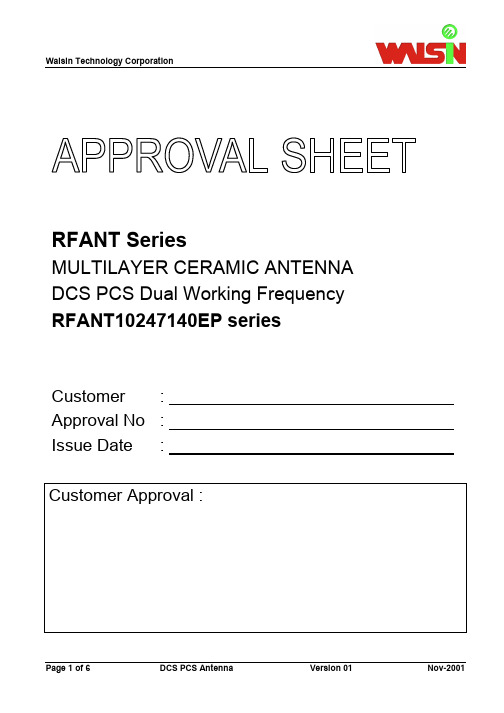
RFANT SeriesMULTILAYER CERAMIC ANTENNA DCS PCS Dual Working Frequency RFANT10247140EP seriesCustomer :Approval No :Issue Date :Customer Approval :FEATURES1. Multilayer LTCC ( Low Temperature Cofired Ceramics ) Technology2. SMD ( Surface Mounted Devices ) TypeSize3. Miniature4. High Stability in Temperature / Humidity Change5. Free Impedence Matching6. Suitable for 900 MHz Working Frequency Operation APPLICATIONS1. DCS 1800 handset2. PCS handset3. PHS 1900 handsetCONSTRUCTIONFig 1. Outline of DCS PCS Dual Band Chip AntennaELECTRICAL CHARACTERISTICSRFANT10247140EP SeriesItem Specification Central frequency 1.85 GHz (*Note 1)MHz Bandwidth 280dBi Gain 0max.VSWR 2Polarization LinearAzimuth Beamwidth Omni-directionalImpedance 50ΩDIMENSIONSFigure Dimension Port definitionL 10.20 ± 0.40 mm -W 4.70 ± 0.30 mm -T 1.40 ± 0.30 mm -Fd 1.00 ± 0.20 mm Feed terminationG 1.00 ± 0.20 mm Ground terminationC 0.50 ± 0.20 mmmax.D 0.50mmP2 1.00 ± 0.20 mm Solder terminationP3 1.00 ± 0.20 mm Solder terminationP4 1.00 ± 0.20 mm Solder termination MARKINGUpon customer requested, max. 5-digit code is allowed.STANDARD TESTING CONDITION1. Unless otherwise specifiedTemperature:15 ~ 35°CHumidity:25%RH ~ 85%RHAtmospheric pressure:86kPa ~ 106kPa2. In case of doubtTemperature : 20±2°CHumidity : 60%RH ~ 70%RHAtmospheric pressure : 86kPa ~ 106kPaRELIABILITY TESTTest itemTest condition / Test methodSpecificationSolderabilitySolder temp.: 230±5°CImmersion time : 2±0.5 sec Solder: SN63 95% min. coverage of all metabolised areaResistance to soldering heatSolder: Sn63Solder Temp. : 260±5°C Immersion time : 30±0.5 secMeasurement to be made after keeping at room temp. for 24±2 hrs.No mechanical damage. Ceramic surface shall not be exposed in the middle of the termination or on the terminated product edge by leaching. Humidity ResistanceHumidity:90% to 95% R.H. Tempertaure:40±2°C Time: 500±24 hours.Measurement: After placing for 24 hours Minimum.No mechanical damage. Samples shall satisfy electrical performance in Table 1.Temperature cycle1. 30 minutes at -55°C ±3°C,2. 10~15minutes at room temperature,3. 30 minutes at +125°±3°C,4. 10~15minutes at room temperature, Five continuous cyclesNo mechanical damage. Samples shall satisfy electrical performance in Table 1.Drop test Height : 75 cm Direction : 3 directionsTimes : 3 times for each direction.No mechanical damage. Samples shall satisfy electrical performance in Table 1.Table 1. Electrical characteristics reliability Center Frequency Initial value +/- 12MHz VSWR within the band3.5max.SOLDERING CONDITIONTypical examples of soldering processes that provide reliable joints without any damage are given in Fig 3.Fig 2. Infrared soldering profileORDERING CODERF ANT 1024714 0 EP T - XXXWalsin RF device ProductcodeANT :AntennaDimension codeLength, Width,Thickness :e.g. :1225119 =Length 122,Width 51,Thickness 19Unit ofdimension0 : 0.1 mm1 : 1.0 mmAntenna typeI: ISM Band/BluetoothantennaD : GSM 900/1800dual bandantennaC : GSM 900antennaE : GSM 1800antennaG : GPS antennaW : WCDMAantennaP : PHS antennaPackingT : 7” ReeledG : 10” ReeledB : BulkX : SFC productCustomercodee.g. : 001 =CF2450MHz,BW120MHz,for customer XAccording to above rule, the product ordering code for DCS PCS Dual Band Chip Antenna is : RFANT10247140EPT-XXXPACKAGINGPlastic Tape specifications (unit :mm)Index Ao Bo ΦD T W Dimension (mm) 5.85 ± 0.10 7.60 ± 0.10 1.55 ± 0.10 0.30 ± 0.10 16.0 ± 0.30 Index E F Po P1 P2 Dimension (mm) 1.75 ± 0.10 7.50 ± 0.10 4.00 ± 0.10 8.00 ± 0.10 2.00 ± 0.10Reel dimensionsIndex A B C DDimension (mm) Φ330 Φ100.0 Φ13.5 16.5±0.1。
GSM0710中文版

CMUX协议文档修订情况记录:目录CMUX协议文档 (1)1. 引言 (4)1.1. 编写目的 (4)1.2. 编写背景 (4)1.3. 参考资料 (4)1.4. 名字解释 (4)2. CMUX协议框架 (5)3. Non Error Recovery Mode (8)3.1. 服务接口定义 (8)3.1.1. 服务模型 (8)3.1.2. 启动CMUX服务模式 (9)3.1.3. 建立DLC服务 (9)3.1.4. 数据服务 (10)3.1.5. 功耗控制 (10)3.1.5.1. Sleep模式 (11)3.1.5.2. Wake up模式 (11)3.1.6. 释放DLC服务 (11)3.1.7. 关闭服务 (11)3.1.8. 控制服务 (11)3.1.8.1. 07.10协议服务 (12)3.1.8.2 虚拟端口服务 (13)3.2. 数据帧结构 (14)3.2.1. 帧域 (14)3.2.1.1. 标志域(Flag Sequence Field) (14)3.2.1.2. 地址域(Address Field) (14)3.2.1.3. 控制域(Control Field) (15)3.2.1.4. 信息域(Information Field) (15)3.2.1.5. 长度指示域(Length Indicator) (15)3.2.1.6. FCS域(Frame Checking Sequence Field) (15)3.2.2. 格式约定 (16)3.2.3. 帧有效性 (16)3.2.4. 帧中止 (16)3.2.5. 数据帧之间的填充 (16)3.2.6. 基本Basic (16)3.2.6.1. 约束 (17)3.2.7. 高级Advanced (17)3.2.7.1. 控制字节透明 (17)3.2.7.2. 开始/停止传输-扩展透明 (17)3.2.7.3. 流控(Flow-control)透明 (18)3.2.7.4. 帧的结构 (18)3.3. 帧类型 (18)3.4. 过程和状态 (20)3.4.1. 建立DLC链路 (20)3.4.2. 释放DLC链路 (20)3.4.3. 信息传输 (21)3.4.4. 帧变量 (21)3.4.5. 超时的考虑 (22)3.4.6. 多路控制通道 (22)3.4.6.1. 控制消息格式 (22)3.4.6.2. 控制消息类型参数 (23)3.4.7. 电源控制与唤醒机制 (32)3.4.8. 流控 (32)3.5. 集成层Convergence Layer (34)3.5.1. 类型1-未结构化的字节流 (34)3.5.2. 类型2-带参数的未结构化的字节流 (34)3.5.3. 类型3-不可中断的帧数据 (36)3.5.4. 类型4-可中断的帧数据 (36)3.6. DLCI值 (37)3.7. 系统参数 (37)3.7.1. 确认时间T1 (37)3.7.2. 帧的最大长度N1 (38)3.7.3. 最大重发次数N2 (38)3.7.4. 窗口大小k (38)3.7.5. 控制通道的响应时间T2 (38)3.7.6. 唤醒流程的响应时间T3 (38)3.8. 启动和关闭MUX (38)4. Error Recovery Mode (39)1. 引言1.1. 编写目的本文档根据GSM07.10协议同时结合E901 Mobile参考代码,对CMUX多串口协议进行了大致的描述。
s3c2410中文手册

s3c2410中文手册简介S3C2410 是一种嵌入式处理器,由韩国三星电子公司设计和制造。
它是一款高度集成的 ARM 架构芯片,广泛应用于各种移动设备中,如智能手机、平板电脑、PDA 等。
本手册将详细介绍 S3C2410 芯片的特性、功能和使用方法,帮助开发人员更好地理解和应用该芯片。
芯片特性S3C2410 芯片具有以下主要特性:1.ARM920T 内核: S3C2410 芯片采用了 ARM920T 内核,它是一种高性能、低功耗的 32 位 RISC 处理器。
ARM920T 内核支持 ARMv4T 指令集,并具有强大的计算和处理能力。
2.高度集成的外设: S3C2410 芯片内集成了许多常用的外围设备,包括 UART、SPI、I2C、PWM 等。
这些外设可满足各种应用需求,简化了系统设计和连接。
3.多种接口: S3C2410 芯片提供了丰富的接口,如LCD 控制器、触摸屏控制器、SDIO 控制器等。
这些接口允许连接各种外部设备,如显示屏、输入设备、存储卡等,实现更丰富的功能。
4.低功耗设计: S3C2410 芯片采用先进的低功耗设计技术,具有很低的静态功耗和动态功耗。
这使得它非常适合于移动设备,延长了电池寿命。
芯片功能GPIOS3C2410 芯片提供了多个 GPIO 管脚,用来实现输入和输出功能。
GPIO 管脚可以通过软件配置为输入模式或输出模式,并可以设置电平状态。
开发人员可以利用GPIO 实现各种功能,如控制 LED 灯、读取按键状态等。
UARTS3C2410 芯片内集成了多个 UART 模块,用于串口通信。
每个 UART 模块都提供了数据传输和接收的功能,并支持多种通信协议,如 RS232、RS485 等。
开发人员可以使用 UART 实现与外部设备的串口通信。
LCD 控制器S3C2410 芯片具有强大的 LCD 控制器,支持多种显示模式和分辨率。
LCD 控制器可以控制显示屏的像素点,实现图形显示和文字显示功能。
昌弘CXN系列统一存储说明书

CHANGHONG CNX系列统一存储CHANGHONG CNX统一存储产品线凭借强大的简单性、现代化的设计、灵活部署和经济实惠的价格,引领闪存存储技术创新。
它致力于满足各种规模数据中心中资源受限的IT专业人员的各项需求。
如果您在寻找功能丰富、使用简便且占用空间小的产品,如果您对成本比较敏感且希望找到更适合的选择,那么CNX统一存储正是适合您的理想解决方案。
CNX统一存储是专为闪存而设计的,配有丰富的数据服务,能够以磁盘的成本优势交付闪存级别的性能。
CHANGHONG CNX统一存储采用功能强大的全新英特尔至强处理器,可实施面向数据块、文件、VMware VVol的整合体系结构,并行支持本机NAS、iSCSI和光纤通道协议。
每个系统均利用多核心存储处理器,完整的12Gb SAS后端连接性的多核体系架构操作环境,从而能提供出色的性能和效率。
可通过磁盘扩展柜添加额外的存储容量。
与之前的CNX型号相比,新一代的CXN统一存储阵列拥有高达2倍的 IOPS、更多的内存、最高多50%的驱动器,它可简化IT转型之路,让您的数据资本充分发挥潜力。
这些全闪存和混合存储系统具有双活控制器体系结构和企业级特性,性能强大,并且进行了效率优化,可实现高达5:1的数据缩减,同时可以帮助您简化多云之旅。
概述如果您在寻找强大的全闪存性能、出色的效率、使用起来很简单而且占用空间小的产品,那么CHANGHONG CNX混合闪存存储正是您的理想之选。
这些新的和现代化的硬件平台专为虚拟化工作负载而设计和优化,与前几代产品相比,可提供更高的性能和更短的延迟,使其非常适合在任何位置运行业务应用程序并在 IT 转型中快人一步。
CNX混合磁盘存储CNX混合闪存阵列一开始就是为了满足市场对混合存储性能、效率和生命周期简易性的需求而设计,支持NVMe,实现双控制器双主动体系结构,搭载双路英特尔处理器,最多可配16个核心和更多系统内存。
与前几代产品相比,所有这些现代化功能使CNX能够提供更高的性能和更少的延迟。
256FBGA中文资料

! ! ! " ! # $ % & '! (( ) * ' ( # ! $ * $$!" ( ( (" * & " + * ( & & ,! ! "# $ ! % & # ' ()*+,-.'/0 1 & (! 1 2 (3- 445 6 1"!$* 78 9 6 & $ * " & & & (" 1 8 9 6 & (.:.1 ;"$ ! & 2!< ( 1& & (< ' & " 1 & & (. < ! & 1 "##- * .* / #! 0 1 # $ ! 23 2 ) & & ! 43 5 * ! 3 5 ((* + * # ! 67 ( 8- ! .1 ( / # ! 422 9: ( $ ; !) & ( & (!" #$ %% ! &! % % #$ %& # 8 ! ' "## + & *96 ! = = 8 + / !)5 ,*5* = & & 6 ' & + 2 2!< "!* & % = & 8 + *! 6 8 > & + = + / !)5 ,*5* = & 8 & (" 1 & & & 7 + & = +3!" ! # $ % & ' '( % )' ) % * +, $ ) $ - ./ -01) $ +) . ) ' +) && ) ) 2 $ # & # $ # ) ) ) & 3 , " ' 2 + 4 ) ') & ./ . 5 $ ) 6 ./. 207 & ./ 42 5 $ ) 6 ./427 & ./ 5 ) +) 5 $ ) 6 ./ 57 & ./ 5 ) 8 99 ) ) 5 $ ) 6 ./ 7 & & ./ * +, * ) 5 $ ) 6 ./*9:7 && ./ 2 + * ) ) 5 $ ) 6 ./2 * 7 & 5 ) ; + 5 ) & ) < ) 3 # 5 ) & 01) ! $ ) 3 # 5 ) %25 . * ) * $ ) 5 $ ) 6 2* =7 25 . * ) 5 ( # 5 $ ) 6 250 7*25 . * ) 3 ) ( ) # 5 $ ) 6 23 7 25 . * ) 3 ) 2 5 $ ) 6 23 4 7. # ! , +) ++ ; + $ 3 ) ) ) $ ) ) + ) % & !) ) + ) % .0. * $ ) 5 $ ) %9*2 ) ' )( * 8< ! + 2 )( $ # 9*2 * ) 9*2 * ) ) ) 8. , 4 ) ') 5 $ ) 9*2 2. 5 $ ) 9*2 2. *( * ) 5 $ ) &9*2 # $ - 5 $ ) & 9*2 # $ 5 $ ) & 9*2 # $ 5 $ ) 9*2 ) 5 $ ) %< ! + ) 5 $ ) -9*2 )) $ )! % 01) $ &-% 5 $ ) &-)% 2. * ' ) &% 01) $ & % 5 $ ) & !"#$!% &'()#&$ * + !"#$!% &'()#&$ * + (# %!,- !"#$!% &'()#&$ * + !"#$!% $&'()#&$ * + . $&/012$(#& $&'()#&$3 ("(#(/% 4/%5& () 6 #/#5) $&'()#&$ * + "#&$$57# #/#5) $&'()#&$ * + &'()#&$ * + % 4 ' ) &% &$(/% /#/ !$0 &%&,# 1 % 01) $ % 5 $ ) !"#$!% &'()#&$ * + #/#5) &'()#&$ * + 8 9 !5"#&$ &'()#&$ *8 9 + 8 /#/ 5::&$ &'()#&$ * 8 ; + 8 /#/ 5::&$ &'()#&$ * 8 ; + &)&# &'()#&$ * &)&# &'+ % # $ % ..*8 4 ' ) % 01) $ % 5 $ ) !<</"0 &'()#&$ * + 00$&)) &'()#&$ * + /#/ $(#& &'()#&$ * + /#/ &/0 &'()#&$ * + !":('5$/#(!" &'()#&$ * + (<("' /$/<&#&$ &'()#&$ * + #/#5) &'()#&$ * + % & 01) $ % & 5 $ ) *#&)# !5#75# $&'()#&$+ *#&)# ("75# $&'()#&$+ = *#&)# ,%!,- $&'()#&$+ ; % +, 2 $ # &% ( ! ' ) &% 0 ' ) 4 651> 17 % 01) $ % &5 $ ) 8 8 ; (, 8 (, 8 (, (, (, ;=!- 01) $ - 5 $ ) !"#$!% &'()#&$ * + !5,> /"&% !"#$!% &'()#&$ * + /##&$? ,>&,- !"#$!% &'()#&$ * + !5"0 !"#$!% &'()#&$ * + "#&$$57# #/#5) &'()#&$ * + (7 !2" !"#$!% #/#5) &'()#&$ * + ($&,# !"#$!% &'()#&$ * + ($&,# /#/ &/0 &'()#&$ * + !5,> /"&% /#/ $&'()#&$ !5,> /"&% /#/ &'()#&$ /(" /##&$? /#/ &'()#&$ * + /,-57 /##&$? /#/ &'()#&$ * + !5"0 /#/ &'()#&$ * . + - 01) $ % - 5 $ ) % @ 3 3 3 3 A @ 3 3 3 3 A @ 3 3 3 3 A = @ 3 3 3 3 A @ 3 3 3 3 A @ 3 3 3 3 A @ 3 3 3 3 A @ 3 3 3 3 A ;8 - +, $ # % - 5 $ ) % "#&$$57# "/B%& &'()#&$ * + "#&$$57# #/#5) &'()#&$ * + &,#!$ &'()#&$ * + !5$,& &,#!$ &'()#&$ * #! + "#&$$57# &'()#&$ * + $(!$(#? &# &'()#&$ * #! + &)# "/B%& $&'()#&$ * + &)# ("#&$$57# $&'()#&$ * + = - & 01) $ - - & 5 $ ) - =&?B!/$0 !":('5$/#(!" &'()#&$ *= + =&?B!/$0 /%5& &'()#&$ *= + =&?B!/$0 /%5& &'()#&$ *= + =&?B!/$0 #/#5) &'()#&$ *= + 1 - 01) $ - - 5 $ ) - 84- '' + ) = ) -% - 01) $ - 5 $ ) /#/ &'()#&$ * + /#,> &'()#&$ * + #/#5) &'()#&$ * + !"#$!% &'()#&$ * + - 01) $ - 5 $ ) (<&$ @ 3 3 A /)& &'()#&$ * @ 3 3 A + (<&$ @ 3 3 A !5"# &'()#&$ * @ 3 3 A ; + (<&$ @ 3 3 A !"#$!% &'()#&$ * @ 3 3 A + (<&$ !7 %&4&% !"#$!% &'()#&$ * + (<&$ #/#5) &'()#&$ * + (<&$ !2&$ B(# /)& &'()#&$ !: B(# !5"#&$ * + (<&$ ;77&$ B(# /)& &'()#&$ !: B(# !5"#&$ * 9 9+ (<&$ B(# !5"#&$ !"#$!% &'()#&$ * + >/""&% @ 3 A !5"# &'()#&$ * @ 3 + ; + >/""&% @ 3 A (0#> &'()#&$ * @ 3 + 9+ >/""&% @ 3 A &$(!0 &'()#&$ * @ 3 + + >/""&% @ 3 A !"#$!% &'()#&$ * @ 3 A + ; 1 - % 01) $ - % 5 $ ) 1 9 1 1 1 ;/$# " - % 4 4 ) ') . ' ) & - - 3 )+( $ # ' ) >& /#,>0!' (<&$ !0& >& "#&$4/% (<&$ !0& (<("' !: )&##("' #>& !4&$:%!2 :%/' (<("' !: ,%&/$("' #>& !4&$:%!2 :%/' - - 5 $ ) !"#$!% &'()#&$ * + #/#5) &'()#&$ * + !5"#&$ * + - - 01 #' 5 $ ) )) $ - "#&$4/% (<&$ !0& /#,>0!' (<&$ !0& 2(#> "#&$"/% &)&# ()/B%& /#,>0!' (<&$ !0& 2(#> /"5/% &)&# ! "-4 3 " 2 " ! ++++++++++++++++++++++++++++++++++++++++++++++++++++++++++++++++++++++*3 4 * " 2 & 7= ++++++++++++++++++++++++++++++++++++++++++++++++++++++++++++++++++++++++++++++++++++++++++++++++++*. 4 ) " 2 ! ; & +++++++++++++++++++++++++++++++++++++++++++++++++++++++++++++++++++++++++*? 4 " 2 78 ; & ++++++++++++++++++++++++++++++++++++++++++++++++++++++++++++++++++)5 - 3 ! ! 78 & ++++++++++++++++++++++++)) . 3 # " & < & ! % & +++++++++++++++++++++++++++++++++++++++++++++++++++++++++++++++++++++ . . * # " & < & & ++++++++++++++++++++++++++++++++++++++++++++++++++++++++++++++++++++++ . . ) 78 ! % # " ! = +++++++++++++++++++++++++++++++++++++++++++++++++++++++ . . 78 ! = ! +++++++++++++++++++++++++++++++++++++++++++++++++++++++++++ ? . 4 78 ! = 7 & # # ++++++++++++++++++++++++++++++++++++++++++++++++++++++++ ? ? 3 ! ++++++++++++++++++++++++++++++++++++++++++++++++++++++++++++++++++++++++++++++++++++++++++++++++++++++++-5 ? * 2!< < ' +++++++++++++++++++++++++++++++++++++++++++++++++++++++++++++++++++++++++++++++++++++++++++++++++++++++,4 ? ) 2!< ! 7 ++++++++++++++++++++++++++++++++++++++++++++++++++++++++++++++++++++++++++++++++++++++++++,- ? 2!< = = ++++++++++++++++++++++++++++++++++++++++++++++++++++++++++++++++++++++++,, 35 3 "!$* ++++++++++++++++++++++++++++++++++++++++++++++++++++35. 35 * "!$* = +++++++++++++++++++++++++++++++++++++++++++++++++++++++35? 35 ) & & ++++++++++++++++++++++++++++++++++++++++++++++++++++++++++++3*, 35 = & ++++++++++++++++++++++++++++++++++++++++++++++++++++++++++++++++3*. 35 4 = & +++++++++++++++++++++++++++++++++++++++++++++++++++++++++++++++++++3)5 35 - & & &6 +++++++++++++++++++++++++++++++++++3)3 35 , & & ++++++++++++++++++++++++++++++++++3)*6 * 3 " ! ++++++++++++++++++++++++++++++++++++++++++++++++++++++++++++++++++++++++++++++++++++++++++++++++++3) 6 * * 78 ! +++++++++++++++++++++++++++++++++++++++++++++++++++++++++++++++++++++++++++++++++++++++++++++++++++34 6 3 = && +++++++++++++++++++++++++++++++++++++++++++++++++++++++++++++++++++++++++++++++++++++++++++++++++++++++3. 6 * " < && ++++++++++++++++++++++++++++++++++++++++++++++++++++++++++++++++++++++++++++++++++++++++++++++3? 6 4 3 " 2 ! +++++++++++++++++++++++++++++++++++++++++++++++++++++++++++++++++++++++++++++++++++++++++++++++++++++*) 6 4 * " 2 < ! & 7= " 2! ++++++++++++++++++++++++++++++++++*. 6 4 ) " 2 < ! ! ; & " 2! ++++++++*? 6 4 " 2 < ! " 2! +++++++++++++++++++++++++++++++++++++++++)5 6 - 3 ! ! +++++++++++++++++++++++++++++++++++++++++++++++++++++++++++++++++++++++++++++++)* 6 - * ! $ && +++++++++++++++++++++++++++++++++++++++++++++++++++++++++++++++++++++++++++++++++++)4 6 - ) ! = ! +++++++++++++++++++++++++++++++++++++++++++++++++++++++++++++++++++++++++++++++++++++++++++++++++++)4 6 , 3 ! ! +++++++++++++++++++++++++++++++++++++++++++++++++++++++++++++++++++++)? 6 . 3 # & & ++++++++++++++++++++++++++++++++++++++++++++++++++++++++ * 6 . * # ! +++++++++++++++++++++++++++++++++++++++++++++++++++++++++++++++++++++++++++++++++++++ * 6 ? 3 ! ++++++++++++++++++++++++++++++++++++++++++++++++++++++++++++++++++++++++++++++++++++43 6 ? * ! ! +++++++++++++++++++++++++++++++++++++++++++++++++++++++++++++++++++++++++++++++++++++4- 6 ? * !" ! ++++++++++++++++++++++++++++++++++++++++++++++++++++++++++++++++++++++++++++++-3 6 ? ) ! & ! +++++++++++++++++++++++++++++++++++++++++++++++++++++++++++++++++++++++++-- 6 ? ! & ! ++++++++++++++++++++++++++++++++++++++++++++++++++++++++++++++++++++++++++++++++++,3 6 ? 4 2!< ! & " +++++++++++++++++++++++++++++++++++++++++++++++++++++++++++++++++++++++++++++++++++++++++++++++++,- 6 ? - 2!< ! & ! > ++++++++++++++++++++++++++++++++++++++++++++++++++++++++++++++++++++++++++++++++++++++++,, 6 ? , 2!< ! = ! +++++++++++++++++++++++++++++++++++++++++++++++++++++++++++++++++++++++++++++,. 6 35 3 ! +++++++++++++++++++++++++++++++++++++++++++++++++++++++++++++++++++++++++++++++++++.* 6 35 * ++++++++++++++++++++++++++++++++++++++++++++++++++++++++++++++++++++++++++++++++++++++?, 6 35 ) ! ++++++++++++++++++++++++++++++++++++++++++++++++++++++++++++++++++++++++++++++?. 6 35 8 9 6 & ! +++++++++++++++++++++++++++++++++++++++++++++++35) 6 35 4 "!$* ! ++++++++++++++++++++++++++++++++++++++++++++++++++++++++++++++++++++++++++++++++35- 6 35 - ! ++++++++++++++++++++++++++++++++++++++++++++++++++++++++++++++++++++++++++++++++++++++++++++++++++333 6 35 , ! ++++++++++++++++++++++++++++++++++++++++++++++++++++++++++++++++++++++++++++++++++++++++++++++++33) 6 35 . 2 $! ! ++++++++++++++++++++++++++++++++++++++++++++++++++++++++++++++++++++++++++++++++++++++++33? 6 35 ? < & = )+-.- /0 > ++++++++++++++++++++++++++++++++3*) 6 35 35 & ! +++++++++++++++++++++++++++++++++++++++++++++++++++++++++++++++++++++++++++++3*.,,*5 .9 & & . & && 6 + 2 - #< & 7 +/ !)5 ,*5* & & = # & # & 6 - 58 .5 @; +/ !)5 ,*5* + & 3- 6 & & 3- - 3*. *4- < ! & = 0 * - <+ && & )* 6 & & = + < & & & & 6 8 && + ! & ! $! & = & ! = 6 & & & = +; !)5 ,*5* 6 0 6 & < & & 6 & 6 ( "< 1+ 6 ; !)5 ,*5*A3+ 6 ( !<1 "2 & &*+ "< 6 & & &)+ "< ( 2 & 6 & & &1 = & 6 +!< & & = 6 & ! + ! && 6 !< & = & 6 # ! = !<+ & & 6 & 6 = & +; !)5 ,*5* & & 6 !< 6 + 6 6 > & & 6 & 6 & + 6 ,*5 > & & & 6 ! 6 0 & + < 6 6 & > & &6 & ( B)A*C D 331 6 ' ! 6 6 ' +! = & !< 6 + 8 & 8+8+8 6 888+= & 6 # + = & 6 && > $ ' & $ ! & 6 + # & "<+ ! 6 6 !< @; > + @ & !< > + !<$= & 6 !< & = ! 6 ' = & +"< 6 + & "< 6 + "< 6 & !< (355 /01 & 2!< & # + + "< 2 ' > )+-.- /0 = "< !< &+"< & + ' & & & 6 & &.+ < "< 6 !< 6 = & & 6 & + "<6 & ' 0 & = & & 6 !< & 2 ' & & 6 +"< < & & & < < & "< + && "< 6 & > & ' & & +! ' ; !)5 ,*5* + ! & = & & !< & 3- 6 & ! + 3- - 3*. 6 83- 6 & = & = 0 * - 6 +!< & = & 6 & & & + = & 6 6 += & && & & > ! + = & 6 0 8 & 3- & + && & 6 ( ! ' && 6 > 1+!"; !)5 ,*5* !<+ < !< 6 6 " !" + ! = !< 6 ! = & 6 ! # & @; +& = ' A3+ 2!<*+ $ & )+ ! &2!< & 6 & 6 & 8 > & + & 2!< 3* 6 $ 3+4 6 $ + & 8 6 $ 5+4 6 $ + & & ..+*9<$ + 6 ! "< & !< 6 & & 0 & = A2!< E & & &! & &! & > & & = ! + 0 6 = 8 ! 6 & & ' 6 & = A2!< )F F ! & 5+,4F8 ! 6 & & ' 6 & = ,+,4F+& ! & 6 ' < & ' 6 + "< = 2!< 6 & & 6 +& "< < & + & = & > G > !<+ & !< > & & & ( & 6 & & 6 1+> & 6 "< 6 & & "< 6 = &$ !< " 7 "<+ ' & & "< 6 "!7# = + & & 6 "! < "< + "< && " & +?"< 6 & = & / % B3A5C ( 1 + !< 6 + 8 & < 7 ( = & "< 1 & ! 6 & < !< +! "& & 888 < " +# $ $%! & "< < & 6 & = "< 6 + / = & = "< 6 + = "< 6 & + & "< 6 & 7 8 .9<$ + E & & 7 +&$ &; !)5 ,*5* & & "< 6 & & 6 + (% 6 > & & +1# !"$ & % ' ( # ) *+ ' , - . $ &# ' % ( # ' # ' ( ) /'0 # ' 1 % # ' % 2#/0% $!" % 0 % % % 2#/0 . ( % $!"/ 3! % $!" /" ++45 ' % 2#/0 . ( % / 3! ! " # !!- % % 2#/0 % !- $ $$ % & '' # &63 % % 2#/0 % 63/ 7 % . % / 8% % % 2#/0 % /() ($ )$#1 % % % 2#/0 % #1 $ * + ,. ( % % 9: ( % 2#/0 % . ( 2 #% 3 != & & 8 & = & + & ;" & +0 3! ;) % %0 !3 4 % % % % - . % -- #$ $ & ( #<< 9;9: 7 % ($% &元器件交易网35/ !)5 ,*5* &= & & = 6 &6 & ' + ! & = + / !)5 ,*5* 6 & 6 ' ' ' = ( & 6 H I ' 1 6 2 & + (" 21 8 &6 & & ! = &+ && & & 6 & & + 6 > ' 6 & 6 + &= & + && & = & & = & 6 & & + / !)5 ,*5* & & 6 & 6 & = = & 6 & " 2 & + "< 6 6 ' & & + 6 & 6 & & & & & 6 & + && ' = 6 &+' ( )* " & "! & # > & & & ' 0 & + 6 & & +' +," 2 (" 21 & = + 6 = A% ! ( % * . , 3"! ". !" 6 &% (/ # $ % % % #$ 3 ! 8% % '3"! ) ( / * # $ % ! & , # $ % % % . % 3"! $ % ' '/ 9;9: 7 #<< 0 ( 7 % ( ( % # $ ( = 3"! ) > ? 3 . % ( )% * >0 ? ( , " ( )% 8% % % # $ / % % )' ( ) &/ !)5 ,*5* & & ( 1 )* 6 = 6 & 6 + ,*5 & & & = & / !)5 ,*5*+ && ,*5 & & 6 (7 6 && & 71 ' J ; 6 & & 6 & 6 && & + 6 & & & 6 & 6 & = +元器件交易网33* +, &- # 4 ) # * $ = ( 5 &>元器件交易网元器件交易网3*3)!6 * * & 6 8 ; !)5 ,*5*+' ' ' ' 00% % 0!! 0% % // %/!! / %/0/ % '0% %/0!! / % '0% % / / % % ## %$ % . % )% 3% . % )% . % %-.& " )&-# * <# * ((<3@+4H A 0 < 3 % ! 4H9H4 6 *% @ H A, % @ H A @ H A < #0< 3 ( %<<#0< 3 % * 6 ,<6#0< 3 % *C 6 ,<! 0< 3 ! * ( 6 ,< 3=-03 < 3 = < 3#<&<=-0 < 3 ( "!@ :H A 0"0 % "3@ +H A /0 "0 %" @ H A 0 "0 % % "0=0"0 % % "1=@ H A 0 "0 =F#"3G /1 . /'0!&00 &/ @+H A/;'+9' "0 <50 3"! ( % %5=@+H A 0 3"! ( % % "! 0 3"! "! % % ! 0 3"! ! % %1=0 3"! % % @+H A 0 3"! % % 3D <0 3"! 3D $0 3"! % 3@+4H A /0 3"! % !!@+:H A 0 3"! % 3 !"=D / 3 ! 8% %3 !! 50 3 ! ( % %$3 3 / $!" % $3 " / $!" % $ / $!" % $ /-@ H A / $!" % $ 0$ @ H A 0 $!" % % $3 " 0 $!" $" 0 $!" 8%2$"/-2 / $!" % * ( )% # $,/"3/-+/ / 3! ) % /"30$ +0 / 3! ) % % !$ &#!/0$ & !$ &-!/0$ & !C33$ &#$ & C 2!<!C $ &#$ & C元器件交易网3- # * <# * ((" #1 @+H A 0 #% % % % / 30 / % % / <50 / ( % %/ 1 0 / % % !/ =E <5/ / . ( %!- F@+H A 0 ! - ( % % % !-"F@+H A / ! - ( % 5 !-0@ H A 03 . ( % % 9 6 &5 !-/@ H A/ . ( % # 303 # "!$* # 503 # (300 % % 3// % <50 ( % %3@ H A /0 * 63 , 1#0 * 63 , 1=0 * 63 ,!<=0 * 63 , <=0 * 63 , 3/ * 63 , =0 * 63 , "=0 * 63 ,!! (! &1"&/ * 63 , "=!3G' &$ G ! F#/0 % F ! F-0 % F ! G#/0 % G ! G-0 % G !3/-@:H A !/!3 % / % !C33!3 #!3 C !C !3 #!3 C!C"=6!3 !/!3 !C333! #3! C !C 3! #3! C!3! "!0 % 3! % % *" ,!3! <!0 % 3! % % *< ,#<<C33@+H A ##<< C #<<C @+H A ##<< C"###<<6/< @ H A !/=. #<< % *+ #<<,#0" !@+4H A /0 2 % % ' % % #0" &@++H A /0 2 % % ' % % #0" @+ H A /0 2 % % ' % % #0" 3@;H A /0 2 % % ' % % ;"#0" =@ :H A/0 2 % % ' % %#0"/ # % % % %# 1!5=$#/ 1 ( )% > )( ? % < % # $ ."= = /0" % * % #0" % #<< ( ,# !3!#05/! 05!# &! 05/ 05" 0 /-/" % " 0 0$0" % % 0 /-/ % 0 0$ 0 % % " $; &C33 @ H A#C % *+ ;C,元器件交易网34- # * <# * ((C @ H A # C % C33@++H A #/0 C % * C,C @++H A #/0 C %C334@+H A #/0 C % 4C % * % C 4C % ,5/%I !2 % % ( " / I !2 % %/%I !2 % % 3//%I !2 % % % J ;300I !2 % % % %#<<=-!&<=/ < #<< #<< ( 0 /-=/%+ & $ )&< 3$ * -- 4-95 !-0 #0" ! 5 !-0+#0" !+;5 !-0 #0" ! B 5 !-0 / 3#0" ! + 5 !-0:/ <5#0" !:++5 !-04$ /- #0" !4+ 5 !-09$ 0$ #0" !9+ 5 !-0 /"30$ +#0" ! +:5 !-/ #0" !;+45 !-/+#0" !B +95 !-/ #0" !+ + 5 !-/ / 1 #0" !+++;5 !-/:/ =E <5#0" !+ +B 5 !-/4$ /- #0" !+ 5 !-/9$ 0$ #0" !+: +5 !-/ /"3/-+#0" !+49; $"/-2#0" & 9B $3 " #0" &+ $ #0" & + $" #0" & $3 " #0" &: $3 3 #0" &4;9 0% #0" ; !- F #0" + B !-"F #0" ; # 3#0" ;B # 5#0" :B+#1 #0" 4B #1 +#0" 9+ +3 !"=D #0" + 3 !! 5#0" ;+ : " #0" B + " #0" + 4+<3;#0" 3 4 <3B #0" 3+ :B <3+ #0" 3 :;<3++#0" 3 : <3+ #0" 3: :9<3+#0" 34元器件交易网3-< 3$ * -- 4-:4<3+:#0" 39 ::<3+4#0" 3 : <&<=-#0" 3;+ :"3+9#0" = + "3+ #0" =++ "3+;#0" = + +"3+B #0" = + B "3 #0" =:+ ;"3 +#0" =4+ 9"3 #0" =9+ 4"3 3 #0" = + :"3 : 39#0" =;+ "3 4 34#0" =B + "3 9 3:#0" =+ + +"3 3 #0" =+++ "3 ; 3 #0" =+ ++B "3 B 3+#0" =+ ++;"3 3 #0" =+:++ "3 + 1##0" =+4++ "1= 1=#0" =+9+++ "1=!<=#0" =+ B9 3* 3/, "= 3/#0" =+;B; 3! * 30, = 30#0" =+B BB 3* , 3- #0" = + <5* <5, <= <5#0" = +B: !-"F+ "�" = B !- F+#0" = +;:"! :#0" = :元器件交易网3,# -(& ,*5 ARM720T Data Sheet ( 55.,1+元器件交易网3.= & = & 6 3 = &&. * /'9: + ; +B 49 . . : . ; . .+ 49 "0 "0 +"0 "0 " 4+ . 4+ "+ : + 49 + ;; ++ ++4 .: .: .:: .:9 .:; ;B9 3"! 3"! +3"! 3"! +" :;.;95#&& *4- 6 > 6 8 + && )* 6 *4 8 && +8 - 6 ! + & ! & 6 & - 6 && & 6 = ! && +&& 6& = & & A !< "< & "<+ 6 && = 6 ) *A " 6 && +-. * !'.; 3"! & 3"! .; + # $ & # $'#<< .; " .; &$ & &% .; : 3 ! & 3 !! & #.; 4 " J .; 6666 .; + < 3< 3.; + + " .; + $ & & $ & .; + % & 0$-3 .; + : / & /.; + 4 & ' #/ .; + 9 &6 !#& #.; +" J .; + 66662 K .4+ " 2 K .4$ & & $ &) !" 3 ! %2 K .4 % & 0$-3 L !" 3 ! %2 K .4: & ) !"3 ! %3 !2 K .44 J :2 )+" .; $+ & $!" + .; + $ & $!" .; 5&3 & 5&3 .; 2#/0 & 2#/0 .; : /- & /- .;4 & / ="!#& #.; 9"J .; 666元器件交易网3?-. * ! ' .; ; " & " .; B !3 & !3.; ! " .; & 13 & 13 .; # & # .; 3 $!" & $!" .; = $!" & $!" .; 6 !- & !- .; !-+ & !-+.; +"J .; : 6666*5/ !)5 ,*5* & & /" & 6 + & & & 8 & 6 +" "$- ) * % #$) ( ," <01 ) ) % % * ," /3<= ) #$ % % * % % ," <==# M 3==# <==# ) N O % % 3"! ) ( %" % # * # )4, # $ # $ ! & % #$ ! & % !" O (,. ,) ## 9 & 6 "##K & ' "## & ' = 6 & & & & 7!7 > +- ) = ** * />= & "##) > 6 6 ?+,-- /0 & .*+? /0+ > - 6 +& & > & & 6 - ' ' ( ' , 331+ 6 - & 6 B4A5C ' & & "##) ' & #9+ & "##) > & ' & 6 & # ' 6 = + 6 - % / !)5 ,*5* 77" & 6 6 B4A5C ' & "##)+ 6 > 6 - A" ! = '" ! ' ' / !)5 ,*5* * & " 7 77" !#77" & 6 " 2 &" / !)5 ,*5* "##) > . )< ' & 6 " 2 6 & = & #9 6 *+5 )' # + > 6 6 )3+4 /0 5 /0+ @ #9 "## & 6 & < 7! = " 2 77" !#77" & + 8 & @ #9 "## 6 6 & 6 +> A3+ ! & 6 @ #9 6 L5K "##37 6 6 ' +*+ = "##3 > 6 +)+ 6 @ #9 6 3 "##37 6 6 + )' & 2!<+ % . /0+ #9 "## & 6 & < 7! = " 2 77" !#77" & + 8 & #9 "## 6 6 & 6 +"& 6 & 6 & 6 + "2*3" 2 & ( & & = 1 & & & & +% &# & & / " !- # 6 4 & # ## ! " ! & & &+ ' ( 8 & 1+ ! +) %"2 & < & & < #9 ( #9 1+**& & 8 !#77" & +)'& " 2 6 6 "2 > 6 +' "2 !< + 7 & 6 & 6 "2 " 2M #7 = " 2 & 2% !# & ' 2 6 = " 2 !#77" 77" !#77" &)''& ! & & ' & + & 6 & #7 & ( " 2 6 = !< 6 & 6 &1+ " 2 6 6 & & ! ( 8 1+ < @ & & ' & 6 & 6 &6 +2 & 6 & 6 77" !#77" & +'' )''77" !#77" & )+-.- /0 & "## & 6 &+ = 6 + )*9/0 + ' & " 2 ' & '+ ' & " 2 '/0 ( ' & = & & 6 .1+ 7= & & & ! & + N N & +!#77" & 77" !#77" & 8 & 6 ' = ( N N ' 1 6 ' 6 & & = + & " 2+# 0 * $ / ) 1 & $&' = & 6 & A7 = 6 ( 7!7 " 972" & & & " & & 1 & *45/0 ' & = & ( '/01 '+ > *45 /0 = & L ' K 6 + " 972" 8 6 & N %N ' +L ' K 6 6 6 = 6 6 "2+ & "##& ' ( 8 1 "2 6 & = = "## & ' 6 "2 & & 6 +" 972" & ' & " & & 6 & " 2 + 7 6 & = & 6 &+' " 972" ( 8 1 & ' A" 7 6 " 972" 6 6 5 6 ? ! +" & & 7!7 $ ! & ( 1 + " 972" = 5835+" L ' K 6 6 3 ( " 972" 6 5835+1+ % / ( ;" & " 972" && ' +7 " 6 & ' G 6 & !9 + ' $ & " ' &$ " 2 ! +6 2 ' 6 " + ! & ' 6 " > " 2 6 '+ " 2 & +&!)'.; +# $ 03=:# $ "*).; + + # $/3 # $ /3 ".; + +;# $&" # $ &% " ".; + # $ ! + # $ " '#<< % " .; + ;# $ <5+9 .+&# $ ( " .; + # $3& B# $ 3 % "# +, + 2 " & 3 +,+ /-4' #$ "$- <01 ) H 0 % "$- <01 % . . + 0 % ( ; 3 )+ H 3 " & ; )+:012131!5=$#03= =<' & +H:)""'11 N+O # $ . 3==# <==## &! 05 # !3!#05 1 N O # $ 3==# <==# # &! 05 # !3!#05 4$ $ . :/ 7 . +"$- .<01 ./3<= .<==# .3==# <==#! % %# +, 1/ 2 " & 3 +,1/4& > =+ = 5 / !)5 ,*5* & = ( = 1 = 5855,*5*55+0123.# +, 2 & )& 2 " & 3 +, 24*' & +H )"+"'1= %+H % +< 7% <#7 6 & 8 6 + 6 & 6 " " < 7O" P & = 6 8 6 ' & 6 < + 6 & & 6# +, 2 & 5 66 & & 2 " & 3 +, 4&$ = & & "## + 6 A ! < + 6 L ' K 6 + & ' 6 ' 6 & , ,+ ; 6 & 8 & & = & 8 & +151!" "= =1617101 111389 0 G- /- "!3!# 0"/- "" /- ""/-2/- "1!5=$#/- "0 G- ! $13 "1!" " ! $:5670 13!3!# 0" ! $ " ! $"/-2 ! $1!5=$# ! $#<< <0 5#<< <0 5#<<+<0 5#0" ! $' & +H + )"+911 "= = 1 N+O % "= = 1 N O P 3 % =. + P = % =. +:"'1- =. # / % ( 1P 3 # $ % # !3!#05 <01+ P = # $ % # !3!#05 <01+ "'1" = / % ( 1P 3 # $ % "+ P = # $ % "1P 3 # $ % "/-2+ P = # $ % "/-2++"'10 = / % ! 5 # $ / % = 1P 3 # $ % # 1!5=$#+ P = # $ % # 1!5=$#/ % N+O % #$ N O ( %% % % 1/<< * % , 1 P - Q + P %1 / % 1 N+O 1P - 1 %+ P ! 1 %1 1 " 1 N+O ;"'"= = = H 1 "= = = * % ,*41P - 1 "= = %+ P ! 1 "= = %1 1 " 1 N+O "'# 6 = H !3#! 0" -0 05 * % ,1P - # 6+ P ! # 6 %1 # 6 / % 1 N+O % 1P - " ( *" , ( )% + P " ( *" , ( )%1 " / % 1 N+O % 4"'"/= * % ,1P - " / ( )% + P " / ( )%1 "/ / % 1 N+O % 1 P - 0 ( Q + P 0 ( 1 0 = / % 1 N+O %"'#<<< ( 1P #<< ( + P #<< % (1 N+O % #<< $ ( "'#<<< ( 1P #<< ( + P #<< % (1 N+O % #<< $ ( 1P < 3 #<< ( +P < 3 #<< % (1 N+O % #<<+ $ ( "'#0" %1 P - #0" Q + P #0"1 N+O % #0"# # +, ( )* ( & 2 " & 3 +,(674& > "##) ' "## & "##3 # '+ ! 8 6 & & > #9 & 6 & > "##3 # '+ (" 1 = 5836+1617101 111389#<< =-!&<=#<<+=-!&<=#<<+ 6"=D:56713#<< $ =#<< 6"=D $#3! =#<< 6"=D' & +H +9)"+4"'1 #<< 0% % % #<< < ( 3 *<3, " #<<#<<+。
CXG1122EN中文资料

– 1 –E01Z20-PSSony reserves the right to change products and specifications without prior notice. This information does not convey any license by any implication or otherwise under any patents or other right. Application circuits shown, if any , are typical examples illustrating the operation of the devices. Sony cannot assume responsibility for any problems arising out of the use of these circuits.CXG1122EN16 pin VSON (Plastic)SP5T GSM Triple-Band/GPRS Antenna SwitchDescriptionThe CXG1122EN is one of a range of low insertion loss, high power MMIC antenna switches for GSM/GPRS triple-band, dual-band (CXG1121TN) and applications. The low insertion loss on transmit means increased talk time as the Tx power amplifier can be operated at a lower output level. On-chip logic reduces the component count and simplifies the PCB layout by allowing the direct connection of the switch to digital baseband control lines with the CMOS logic levels.This switch is an SP5T , one antenna can be routed to either of the 2 Tx or 3 Rx ports. It requires 3 CMOS control lines (CTL1, CTL2 and Tx ON).The Sony's GaAs JFET process is used for low insertion loss. An evaluation PCB is available.Features•Insertion loss: (Tx) 0.5dB typ. at 34dBm (GSM900)•3 CMOS compatible control lines•Low second harmonic: –40dBm typ. at 34dBm (GSM900)•Small package size: 16-pin VSON (2.7mm × 3.5mm × 0.9mm)ApplicationsT riple-band handsets using the combinations of followings:•GSM900/DCS1800/PCS1900•GPRS •DECTStructureGaAs J-FET MMICAbsolute Maximum Ratings (T a = 25°C)•Bias voltage V DD 7V •Control voltageV CTL 5V •Operating temperatureT opr–20 to +80°CGaAs MMICs are ESD sensitive devices. Special handling precautions are required.– 2 –Pin ConfigurationANT GND Tx1GND Tx2GND V DD Tx ONRx1GND Rx2GND Rx3GND CTL1CTL2Truth TableCTL1H L H L LOn PassANT – Tx1 GSM900ANT – Tx2 DCS1800 & PCS1900ANT – Rx1 GSM900/DCS1800/PCS1900ANT – Rx2 GSM900/DCS1800/PCS1900ANT – Rx3 GSM900/DCS1800/PCS1900CTL2Don't care Don't careL L HTx ON H H L L L– 3 –Electrical characteristics(T a = 25°C)Unit dB dB dB dB dB dB dB dB dBdBm dBm dBmµA mAMax.0.71.20.851.41.4–36–301201T yp.0.51.00.651.21.2201625201.2–40–3436800.3Min.18142318Condition ∗1∗2∗3∗4∗5∗3∗4, ∗5∗1∗2∗1, ∗2∗1, ∗2V CTL = 3.0V V DD = 3.3V PathTx1, Tx2 – ANT Tx1, Tx2 – ANTRx1 – ANT Rx2 – ANT Rx3 – ANT ANT – Tx1, Tx2Tx – Rx1, Rx2, Rx3Tx – Rx1, Rx2, Rx3Tx1, Tx2 – ANT Tx1, Tx2 – ANTSymbolILISOVSWR 2fo 3fo P 1dB I CTL I TX /I RXItemInsertion lossIsolationVSWR Harmonics ∗P 1dB compression input power Control current Supply current for Tx and Rx modesElectrical characteristics are measured with all the RF ports terminated in 50Ω.∗Harmonics measured with Tx inputs harmonically matched. It is recommended that the harmonic matching is used to ensure the optimum performance.∗1Power incident on GSM Tx, Pin = 34dBm, 880 to 915MHz, V DD = 3.3V , GSM Tx enabled∗2Power incident on DCS/PCS Tx, Pin = 32dBm, 1710 to 1910MHz, V DD = 3.3V , DCS/PCS Tx enabled ∗3Power incident on ANT , Pin = 10dBm, 925 to 960MHz, V DD = 3.3V , GSM Rx enabled ∗4Power incident on ANT , Pin = 10dBm, 1805 to 1880MHz, V DD = 3.3V , DCS Rx enabled ∗5Power incident on ANT , Pin = 10dBm, 1930 to 1990MHz, V DD = 3.3V , PCS Rx enabledSupply Voltage Value (V DD )ModeGSM/DCS Tx GSM/DCS/PCS RxMin.3.02.7T yp.3.33.0Max.3.53.5Unit V VLogicHigh LowMin.2.40T yp.2.8Max.3.20.4Unit V VCMOS Logic ValueDC Block Capacitors and Decoupling CapacitorsNote)Capacitors are required on all the RF ports for DC blocking (22pF – 47pF). Decoupling capacitors are required on V DD and on control lines.– 4 –– 5 –Application NoteImpedance Matching for Harmonic MinimizationThis note outlines the method used to find the source impedance to present to a transmit port at the second harmonic frequency (2fo) to reduce the second harmonic level at the antenna.This should be carried out for a set of devices that represent the process variants. This way a compromise can be found that suits all the variants.The necessary equipment is shown immediately below.The device should be mounted on a PCB with 50Ω tracks running from all the RF pins to SMA connectors on the PCB edge (DUT). All the ports should be externally DC blocked and the unused ports should be terminated in 50Ω. All the measurements should be performed at the incident powers for which the harmonic levels are specified in this document.The 2nd harmonic level at the antenna port is measured using the spectrum analyzer and the vertical and horizontal position of the load pull stub adjusted such that this level is minimized.The device should then be removed from the board and an SMA connector mounted such that the source impedance seen by the transmit port at 2fo can be measured using a VNA.Measurements should be de-embedded to the end of the SMA center pin.A network should then be designed to match the impedance of the low pass filter (LPF), which usually comes in front of the device, to the 2fo source impedance that gives sufficiently reduced 2fo levels for all the devices measured.The network should be designed to maintain a good match and insertion loss at the fundamental frequency.Signal GeneratorB.P .F .10dB CouplerPower MeterDiplexerDC BlockD.U.T.DC BlockSpectrum AnalyzerLoad Pull TunerFundamental, fo Second Harmonic, 2fo– 6 –Package Outline Unit: mmSony CorporationSONY CODE EIAJ CODE JEDEC CODEPACKAGE MATERIALLEAD TREATMENT LEAD MATERIAL PACKAGE MASSEPOXY RESIN SOLDER PLATING COPPER ALLOY P ACKAGE STRUCTURE16PIN VSON (PLASTIC)VSON-16P-010.02 gTERMINAL SECTIONranges of 0.1mm and 0.25mm from the end of a terminal.NOTE: 1) The dimensions of the terminal section apply to the+ 0.1LEAD PLATING SPECIFICATIONSITEMLEAD MA TERIAL COPPER ALLOY SOLDER COMPOSITION Sn-Bi Bi:1-4wt%PLA TING THICKNESS5-18µmSPEC.。
1024(金刚)控制台-中文说明书

1024DMX控制器用户手册目录1综述1.1功能描述1.2规格参数2安装2.1设备与附件2.2注意事项2.3连接灯具3操作使用3.1面板图3.2常用词汇介绍4配接4.1创建4.1.1配接常规灯4.1.2配接电脑灯4.1.3查看配接信息4.2编辑4.2.1重新配接灯具地址码4.2.2删除配接4.2.3灯具参数5控制灯具5.1灯具的选择与反选5.2修改属性值5.3灯具区推杆功能的切换5.4电脑灯的高级控制5.5扇形6图形生成器6.1图形调用6.2图形编辑6.3图形删除6.4改变图形运行方向6.5重演参数7单步场景7.1创建7.2导入7.3复制7.4删除7.5时间7.6运行8多步场景8.1创建8.2删除步8.3步时间8.4导入步8.5全局时间8.6删除场景8.7复制场景8.8运行8.9连接8.10高级控制选项9素材9.1存储素材9.2调用素材9.3删除素材10设置10.1擦除重演数据10.2擦除所有数据10.3语言切换11升级12灯库编辑器1综述1.1功能描述1024 电脑灯光控制台可同时控制96台电脑灯。
读取珍珠R20格式灯库,内置图形效果,轻松实现X/Y走圆,RGB彩虹效果,光束波浪式亮暗等效果。
能同时运行10个场景、执行5个内置图形,可使用推杆运行场景并调整场景的调光通道的亮度等级。
1.2规格参数21.1设备与附件产品包装箱内物件清单:●KingKong1024 电脑灯控台1台●光盘1份●电源线一条选配:●航空箱●鹅颈灯●U盘1.2注意事项●务必使用12V的电源适配器●请注意防潮防尘1.3连接灯具●控台台后板有4个DMX512 输出信号卡侬座,两个为三芯XLR 结构,另两个位五芯XLR结构。
卡侬座的1 脚为信号地线,2 脚为信号负端,3 脚为信号正端。
●DMX512 连接电缆采用屏蔽式双绞电缆。
电缆的两端需自行焊接XLR 插头,屏蔽网接XLR 插头的第1 脚,双绞线(由不同颜色区分)则分别连接XLR 插头的2、3 脚,切勿反接。
TEG1024G说明书

版 权 声 明是深圳市吉祥腾达科技有限公司注册商标。
文中提及到的其它商标或商品名称均是他们所属公司的商标或注册商标。
本产品的所有部分,包括配件和软件,其版权属深圳市吉祥腾达科技有限公司所有,在未经过深圳市吉祥腾达科技有限公司许可的情况下,不得任意拷贝、抄袭、仿制或翻译成其它语言。
本手册中的所有图片和产品规格参数仅供参考,随着软件或硬件的升级会略有差异,如有变更,恕不另行通知,如需了解更多产品信息,请浏览我们的网站:1. 产品简介TEG1016G/TEG1024G是专为解决网吧或企业网络数据传输瓶颈的机架式全千兆以太网交换机,提供16/24个10/100/1000Mbps自适应RJ-45端口,支持平行/交叉双绞线自动识别功能,既可当作普通端口连接到PC 等千兆终端,也可以用作Uplink端口级联千兆骨干网络。
使用TEG1016G/TEG1024G替换原有的百兆交换机,可以通过千兆连接解决服务器与客户端的带宽瓶颈问题,也可以作为主干交换机接入到企业或者网吧的千兆局域网中,大幅提升部门与部门之间、终端与服务器之间的传输速率,是一款性价比极高的千兆交换机产品。
1.1交换机特性¾符合IEEE802.3、IEEE802.3u、IEEE802.3ab、IEEE 802.3x标准;¾流控方式:全双工采用IEEE 802.3x 标准,半双工采用Backpressure 标准;¾16/24个千兆自适应RJ-45端口,支持802.3 NWay 自动协商; ¾每个RJ-45端口支持自动翻转功能(Auto-MDI/MDIX);¾MAC地址学习、自动老化;¾采用存储转发机制;¾支持高达32Gbps/48Gbps的背板带宽;¾每个端口的转发速率可达1488095pps;¾支持8K的MAC地址表;¾内置高性能电源。
1.2物品清单请检查产品包装盒内的内容物是否完整,应该包括以下物品: ¾以太网交换机一台¾电源线一条¾产品使用说明书一本¾产品保修卡一张¾L型支架一套(包括两个支架和配套螺丝)¾脚垫四个(上列清单仅供您参考,实际物品清单以出货为准)1.3 产品外观前面板包括:16/24个RJ-45状态指示灯和一个POWER电源指示灯,16/24个 RJ-45端口。
FPGA可编程逻辑器件芯片XC2VP100-6FF1704C中文规格书
Chapter1 Configuration OverviewConfiguration Modes and PinsVirtex®-5 devices are configured by loading application-specific configuration data—thebitstream—into internal memory. Because Xilinx FPGA configuration memory is volatile,it must be configured each time it is powered-up. The bitstream is loaded into the devicethrough special configuration pins. These configuration pins serve as the interface for anumber of different configuration modes:∙Master-serial configuration mode∙Slave-serial configuration mode∙Master SelectMAP (parallel) configuration mode (x8 and x16 only)∙Slave SelectMAP (parallel) configuration mode (x8, x16, and x32)∙JTAG/Boundary-Scan configuration mode∙Master Serial Peripheral Interface (SPI) Flash configuration mode∙Master Byte Peripheral Interface Up (BPI-Up) Flash configuration mode(x8 and x16 only)∙Master Byte Peripheral Interface Down (BPI-Down) Flash configuration mode(x8 and x16 only)The configuration modes are explained in detail in Chapter2, “Configuration Interfaces.”The specific configuration mode is selected by setting the appropriate level on thededicated Mode input pins M[2:0]. The M2, M1, and M0 mode pins should be set at aconstant DC voltage level, either through pull-up or pull-down resistors, or tied directly toground or V CC_CONFIG. The mode pins should not be toggled during and afterconfiguration. See Table2-1, page37 for the mode pin setting options.The terms Master and Slave refer to the direction of the configuration clock (CCLK):∙In Master configuration modes, the Virtex-5 device drives CCLK from an internaloscillator. To get the desired frequency, BitGen -g ConfigRate is used. The“BitGen” section of the Development System Reference Guide provides moreinformation. After configuration, the CCLK is turned off unless the persist optionis selected or SEU detection is used. The CCLK pin is 3-stated with a weak pull-up.∙In Slave configuration modes, CCLK is an input.The JTAG/Boundary-Scan configuration interface is always available, regardless of theMode pin settings. The JTAG/Boundary-Scan configuration mode disables all otherconfiguration modes to prevent conflicts between configuration interfaces.Certain pins are dedicated to configuration (Table1-1), while others are dual-purpose(Table1-2). Dual-purpose pins serve both as configuration pins and as user I/O afterconfiguration. Dedicated configuration pins retain their function after configuration.Configuration Sequencepin and restarting the configuration process from the beginning. The JTAG interface is still responsive and the device is still alive, only the BPI/SPI interface is inoperable. InSelectMAP modes, either the PROGRAM_B pin can be pulsed Low or an ABORT sequence can be initiated (see “SelectMAP Configuration Interface” in Chapter 2).Virtex-5 devices use a 32-bit CRC check. The CRC check is designed to catch errors in transmitting the configuration bitstream. There is a scenario where errors in transmitting the configuration bitstream can be missed by the CRC check: certain clocking errors, such as double-clocking, can cause loss of synchronization between the 32-bit bitstream packets and the configuration logic. Once synchronization is lost, any subsequent commands are not understood, including the command to check the CRC. In this situation, configuration fails with DONE Low and INIT_B High because the CRC was ignored. In BPI Modes, the address counter eventually overflows or underflows to cause wraparound, which triggers fallback reconfiguration (see “Fallback MultiBoot,” page 153).Startup (Step 8)After the configuration frames are loaded, the bitstream instructs the device to enter the startup sequence. The startup sequence is controlled by an 8-phase (phases 0–7) sequential state machine. The startup sequencer performs the tasks outlined in Table 1-15.The specific order of startup events (except for EOS assertion) is user-programmablethrough BitGen options (refer to the Development System Reference Guide ). Table 1-15 shows the general sequence of events, although the specific phase for each of these startup events is user-programmable (EOS is always asserted in the last phase). Refer to Chapter 2, “Configuration Interfaces” for important startup option guidelines. By default, startup events occur as shown in Table 1-16.Figure 1-11:Startup Sequence (Step 8)Table 1-15:User-Selectable Cycle of Startup Events PhaseEvent1–6Wait for DCMs to Lock (optional)1–6Wait for DCI to Match (optional)1–6Assert Global Write Enable (GWE), allowing RAMs and flip-flops to change state 1–6Negate Global 3-State (GTS), activating I/O 1–6Release DONE pin 7Assert End Of Startup (EOS)UG191_c1_10_050406StepsChapter 1:Configuration OverviewSelectMAP Configuration Interface The RDWR_B signal is ignored while CS_B is deasserted. Read/write control of the3-stating of the data pins is asynchronous. The FPGA actively drives SelectMAP datawithout regard to CCLK if RDWR_B is set for read control (RDWR_B=1, Readback) while CS_B is asserted.CCLKAll activity on the SelectMAP data bus is synchronous to CCLK. When RDWR_B is set for write control (RDWR_B=0, Configuration), the FPGA samples the SelectMAP data pins on rising CCLK edges. When RDWR_B is set for read control (RDWR_B=1, Readback), the FPGA updates the SelectMAP data pins on rising CCLK edges.In Slave SelectMAP mode, configuration can be paused by stopping CCLK (see “Non-Continuous SelectMAP Data Loading”).BUSYBUSY is an output from the FPGA indicating when the device is ready to drive readback data. Unlike earlier Virtex devices, Virtex-5 FPGAs never drive the BUSY signal Highduring configuration, even at the maximum configuration frequency with an encrypted bitstream. The Virtex-5 device only drives BUSY High during readback. (For details, refer to Chapter7, “Readback and Configuration Verification.”)∙If BUSY = 0 during readback, the SelectMAP data pins are driving valid readback data.∙If BUSY = 1 during readback, the SelectMAP data pins are not driving valid readback data.When CS_B is deasserted (CS_B=1), the BUSY pin is placed in a High-Z state.BUSY remains in a High-Z state until CS_B is asserted. If CS_B is asserted before power-up (that is, if the pin is tied to ground), BUSY initially is in a High-Z state, then driven Low after POR finishes, usually a few milliseconds (T BUSY), after V CCINT reaches V POR but before INIT_B goes High.Unless readback is used, the BUSY pin can be left unconnected.Continuous SelectMAP Data LoadingContinuous data loading is used in applications where the configuration controller can provide an uninterrupted stream of configuration data. After power-up, the configuration controller sets the RDWR_B signal for write control (RDWR_B=0) and asserts the CS_B signal (CS_B=0), causing the device to drive BUSY Low (this transition is asynchronous).RDWR_B must be driven Low before CS_B is asserted, otherwise an ABORT occurs (see “SelectMAP ABORT”).On the next rising CCLK edge, the device begins sampling the data pins. Only D[0:7] are sampled by Configuration until the bus width is determined. See “Bus Width AutoDetection” for details. After bus width is determined, the proper width of the data bus is sampled for the Synchronization word search. Configuration begins after thesynchronization word is clocked into the device.After the configuration bitstream is loaded, the device enters the startup sequence. The device asserts its DONE signal High in the phase of the startup sequence that is specified by the bitstream (see “Startup (Step 8)” in Chapter1). The configuration controller should continue sending CCLK pulses until after the startup sequence has finished. (This canChapter 2:Configuration Interfaces。
XP1024-BD中文资料

S12,Vd = 4.5V, Vg = 0.6V, Id1 = 216mA, Id3 = Id4 = 440mA
0 -5 -10 -15 -20 -25 -30 -35 -40 -45 -50 -55 -60 -65 -70 -75 -80 0 2 4 6 8 10 12 14 16 18 20 22 24 26 28 30 32 34 36 38 40 42 44 46 48 50 Frequency (GHz)
Mimix Broadband, Inc., 10795 Rockley Rd., Houston, Texas 77099 Tel: 281.988.4600 Fax: 281.988.4615
Page 1 of 7
Characteristic Data and Specifications are subject to change without notice. ©2007 Mimix Broadband, Inc. Export of this item may require appropriate export licensing from the U.S. Government. In purchasing these parts, U.S. Domestic customers accept their obligation to be compliant with U.S. Export Laws.
+6.0 VDC 1700 mA +0.3 VDC +5 dBm -65 to +165 OC -55 to MTTF TAble4 MTTF Table 4
(4) Channel temperature affects a device's MTTF. It is recommended to keep channel temperature as low as possible for maximum life.
KINGKONG1024金刚1024使用说明
金刚1024 King Kong 1024DMX控制器DMX Console用户手册目录1综述1.1功能描述1.2规格参数2安装2.1设备与附件2.2注意事项2.3连接灯具3操作使用3.1面板图3.2常用词汇介绍4配接4.1创建4.1.1配接常规灯4.1.2配接电脑灯4.1.3查看配接信息4.2编辑4.2.1重新配接灯具地址码4.2.2删除配接4.2.3配接效用5控制灯具5.1灯具的选择与反选5.2修改属性值5.3电脑灯的高级控制5.4扇形6图形生成器学习好帮手6.1图形调用6.2图形编辑6.3图形删除7单步场景7.1创建7.2导入7.3复制7.4删除7.5时间7.6运行8多步场景8.1创建8.2删除步8.3步时间8.4导入步8.5全局时间8.6删除场景8.7复制场景8.8运行8.9连接9设置9.1擦除重演数据9.2擦除所有数据9.3语言切换学习好帮手1.1功能描述KingKong1024 电脑灯光控制台可同时控制96台电脑灯。
读取珍珠R20格式灯库,内置图形效果,轻松实现X/Y走圆,RGB彩虹效果,光束波浪式亮暗等效果。
能同时运行10个场景、执行5个内置图形,可使用推杆运行场景并调整场景的调光通道的亮度等级。
1.2规格参数学习好帮手1.1设备与附件产品包装箱内物件清单:●KingKong1024 电脑灯控台1台●说明书1本●电源适配器一个1.2注意事项●务必使用12V的电源适配器●请注意防潮防尘1.3连接灯具●控台台后板有2个DMX512 输出信号插座,为三芯XLR 结构。
这两个插座的1 脚为信号地学习好帮手DMX512 连接电缆采用屏蔽式双绞电缆。
电缆的两端需自行焊接XLR 插头,屏蔽网接XLR 插头的第1 脚,双绞线(由不同颜色区分)则分别连接XLR 插头的2、3 脚,切勿反接。
学习好帮手学习好帮手3.操作使用学习好帮手学习好帮手3.1 面板图该控台主要由若干个区组成:● 灯具区:由16个灯具键、16根推杆和6个灯具换页键组成。
1024芯片
1024芯片
1024芯片,也被称为1K芯片,是一种常见的集成电路芯片。
它通常用于存储数据,其中每个芯片包含1024个存储单元或
存储位,每个存储单元可以存储一个位(0或1)的信息。
1024芯片被广泛应用于计算机、通信设备和其他电子设备中。
它们可以用于存储程序、数据和各种配置信息。
当需要存储大量数据时,可以使用多个1024芯片组成一个更大的存储器。
每个存储单元在1024芯片内部是通过电子开关来实现的。
当
开关关闭时,表示存储位的值为1;当开关打开时,表示存储
位的值为0。
通过控制这些开关的状态,可以读取、写入和擦
除存储位的值。
1024芯片具有很高的存储密度和读写速度。
它们通常与其他
逻辑电路和控制器组合使用,以实现复杂的功能和任务。
与其他芯片相比,1024芯片具有较低的成本和相对较低的功耗。
在计算机科学中,1024芯片还可以用于表示二进制数字。
由
于每个存储位只能表示0或1的值,因此一个1024芯片可以
表示1024位的二进制数字。
这在计算机编程和数据处理中非
常有用。
总之,1024芯片是一种常见的集成电路芯片,用于存储数据
和表示二进制数字。
它们在计算机和电子设备中有着广泛的应用,并具有高性能、低成本和低功耗的特点。
S3C2410中文手册第9章 IO端口

第九章I/O端口概述S3C2410有117个多功能的输入输出引脚,这些端口是:—端口A(GPA):23个输出口—端口B(GPB):11个输入输出口—端口C(GPC):16个输入输出口—端口D(GPD):16个输入输出口—端口E(GPE):16个输入输出口—端口F(GPF):8个输入输出口—端口G(GPG):16个输入输出口—端口H(GPH):11个输入输出口每个端口可以根据系统配置和设计需求通过软件配置成相应的功能。
在启动主程序之前,必须定义好每个引脚的功能。
如果某个引脚不用作复用功能,则可以将它配置成IO脚。
初始的引脚状态被无缝配置好的以避免产生问题。
表1 端口配置见英文版Table 9-1. S3C2410A Port Configuration端口控制描述端口控制寄存器(GPACON-BGHCON)在S3C2410中,大部分端口都是复用的,因此需要决定每个引脚使用哪个功能。
端口控制寄存器PnCON决定每个引脚的功能。
如果GPF0 – GPF7 and GPG0 – GPG7用于掉电模式的唤醒信号,这些端口必须被配置成中断模式。
端口数据寄存器(GPADAT-GPHDAT)如果端口被配置成输出端口,可以向PnDAT中的相关位写入数据;如果端口被配置成输入端口,可以从PnDAT中的相关位读入数据。
端口上拉电阻寄存器(GPBUP-GPHUP)端口上拉电阻寄存器控制每个端口组的上拉电阻的使能和禁止。
当相关位为0,上拉电阻使能;当相关位为1,上拉电阻禁止;当端口上拉电阻寄存器使能时,不管引脚选择什么功能(输入、输出、数据、外部中断等),上拉电阻都工作。
外部中断控制寄存器(EXTINTN)24个外部中断可响应各种信号请求方式。
EXTINTn寄存器可以配置如下信号请求方式:低电平触发、高电平触发、上升沿触发、下降沿触发、双边沿触发。
这8个外部中断引脚具有数字滤波器。
(见EINTFLTn相关)只有16个外部中断引脚(EINT [15:0])被用于唤醒源。
- 1、下载文档前请自行甄别文档内容的完整性,平台不提供额外的编辑、内容补充、找答案等附加服务。
- 2、"仅部分预览"的文档,不可在线预览部分如存在完整性等问题,可反馈申请退款(可完整预览的文档不适用该条件!)。
- 3、如文档侵犯您的权益,请联系客服反馈,我们会尽快为您处理(人工客服工作时间:9:00-18:30)。
8 0.65 ± 0.12
+ 0.05 0.15 – 0.02
0.1 ± 0.1
CXG1024N
0.5 ± 0.2
0° to 10°
DETAIL A NOTE: Dimension “∗” does not include mold protrusion.
SONY CODE EIAJ CODE JEDEC CODE
Test Condition
∗2 Pin=30 dBm
∗2 Pin=20 dBm
∗2 Pin=20 dBm
∗2 Pin=20 dBm
Frequency
1 GHz 1.5 GHz 2 GHz 1 GHz 1.5 GHz 2 GHz 1 GHz 1.5 GHz 2 GHz 1 GHz 1.5 GHz 2 GHz
Applications Antenna switch for digital cellular telephones
Structure GaAs J-FET MMIC
Function Block Diagram
Diversity Antenna 2
Diversity Antenna 1
Antenna 2 TX
(Ta=25 °C) Max. Unit 0.65 0.8 1.0 0.8 0.95 1.2
dB 0.9 1.05 1.5 0.7 0.8 1.0
dB
1.5
1.5
dBm
200 nsec µA
100 µA
100
—3—
Insertion Loss [dB]
元器件交易网
Insertion Loss and Isolation vs. Frequency (RF3–RF2, RF3–RF4)
V
• Operating temperature Topr –35 to +85 °C
• Storage temperature Tstg –65 to +150 °C
• Input Power Pin (RF2, RF3, RF4) 37 dBm
Pin (RF1, RF5, RF6) 30 dBm
Supply voltage
Symbol Vctl (H) Vctl (L) Vctl (H)–Vctl (L)
VDD
Min. –6 Vctl (H)–0.6
Typ. Vctl (H)–0.5
Max. 6
6 Vctl (H)–0.4
—2—
元器件交易网
CXG1024N
Electrical Characteristics Symbol
RX Antenna 1
Sony reserves the right to change products and specifications without prior notice. This information does not convey any license by any implication or otherwise under any patents or other right. Application circuits shown, if any, are typical examples illustrating the operation of the devices. Sony cannot assume responsibility for any problems arising out of the use of these circuits.
元器件交易网
Insertion Loss and Isolation vs. Frequency (RF5–RF1, RF5–RF6)
0 Insertion Loss
0.4
0.8 Isolation
1.2
1.6
CXG1024N 0 –10 –20 –30 –40
0
0.3 0.6 0.9 1.2 1.5 1.8 2.1 2.4 2.7 3
MMIC to connect TX/RX to one of 4 antennas. This IC is designed using the Sony’s GaAs J-FET process and operates at a single positive power supply.
16 pin SSOP (Plastic)
—1—
E96526-TE
元器件交易网
Pin Configuration and Recommended Circuit
CXG1024N
100pF
1
RF1
100pF 100pF 100pF
CTLC VDD RF2
GND
100pF 100pF
CTLB
RF3 100kΩ
GND 8
CTLC
CTLB CTLA
CTLB
CTLD
16 RF6
CTLD
GND
RF5 100kΩ
GND
CTLA CTLA
RF4
GND 9
100pF 100pF 100PF
100pF 100pF
Logic Table
ON-Port RF3–RF2 RF3–RF4 RF5–RF2 RF5–RF4 RF5–RF6 RF5–RF1
1.3
Pin=30 dBm
∗2
0.1 to 2 GHz
1.3
Pin=20 dBm
∗3
1.5 GHz
30
32
∗2
1.5 GHz
33
35
∗1
1.5 GHz
35
37
∗3
1.5 GHz
22
24
∗2
1.5 GHz
25
27
∗1
1.5 GHz
27
29
0.1 to 2 GHz
∗2
∗2 ∗3 : Vctl (H)=3 V, Vctl (L)=0 V, VDD=2.5 V
Features
• Single positive power supply operation
• Low insertion loss 0.4 dB (Typ.) at 1.0 GHz
(TX Port)
• Isolation
21 dB (Typ.) at 1.0 GHz
(TX Port)
• High power switching
Frequency [GHz]
—5—
元器件交易网
Package Outline Unit : mm
16PIN SSOP (PLASTIC)
∗5.0 ± 0.1
16
9
A
+ 0.2 1.25 – 0.1
0.1
∗4.4 ± 0.1 6.4 ± 0.2
1
+ 0.1 0.22 – 0.05
元器件交易网
CXG1024N
High-Frequency SPDT Antenna Switch
For the availability of this product, please contact the sales office.
Description The CXG1024N is a high power antenna switch
0.1g
—6—
Signal Passes
RF3–RF2 RF3–RF4
Insertion Loss
RF5–RF2 IL.
RF5–RF4
Isolation
VSWR
1 dB Compression Power Switching Time Control Current
RF5–RF1 RF5–RF6
ISO.
RF3–RF2 RF3–RF4 RF5–RF2 RF5–RF4
RF5–RF1 RF5–RF6
RF3–RF2 RF3–RF4 RF5–RF2 VS. RF5–RF4 RF5–RF1 RF5–RF6
P1 dB tSW
RF3–RF2
RF3–RF4
RF5–RF2 RF5–RF4 RF5–RF1 RF5–RF6
Ictl
பைடு நூலகம்
Supply Current
IDD
∗1 : Vctl (H)=5 V, Vctl (L)=0 V, VDD=4.5 V ∗2 : Vctl (H)=4 V, Vctl (L)=0 V, VDD=3.5 V
0
0
0.4
Insertion Loss
–10
0.8
–20
Isolation
1.2
–30
1.6
–40
Isolation [dB]
Insertion Loss [dB]
0
0.3 0.6 0.9 1.2 1.5 1.8 2.1 2.4 2.7 3
Frequency [GHz]
—4—
Insertion Loss [dB] Isolation [dB]
Min. Typ.
0.4 0.5 0.7 0.5 0.65 0.9 0.6 0.75 1.2 0.4 0.5 0.7
∗2 Pin=30 dBm
1 GHz 1.5 GHz 2 GHz
18
21
15
18
12
15
∗2 Pin=20 dBm
1 GHz 1.5 GHz 2 GHz
21
24
17
20
15
18
∗2
0.1 to 2 GHz
0 Insertion Loss
0.4
0.8 Isolation
1.2
1.6
Isolation [dB]