S78L18中文资料
78L系列稳压芯片资料

1/24July 2003s OUTPUT CURRENT UP TO 100mAsOUTPUT VOLTAGES OF 3.3;5;6;8;9;10;12;15;18;20;24Vs THERMAL OVERLOAD PROTECTION s SHORT CIRCUIT PROTECTIONsNO EXTERNAL COMPONENTS ARE REQUIREDsAVAILABLE IN EITHER ±5%(AC)OR ±10%(C)SELECTIONDESCRIPTIONThe L78L00series of three-terminal positive regulators employ internal current limiting and thermal shutdown,making them essentially indestructible.If adequate heat-sink is provided,they can deliver up to 100mA output current.They are intended as fixed voltage regulators in a wide range of applications including local or on-card regulation for elimination of noise and distribution problems associated with single-point regulation.In addition,they can be used with power pass elements to make high-current voltage regulators.The L78L00series used as Zener diode/resistor combination replacement,offers an effective output impedance improvement of typically twoorders of magnitude,along with lower quiescent current and lower noise.L78L00SERIESPOSITIVE VOLTAGEREGULATORSL78L00SERIES2/24ABSOLUTE MAXIMUM RATINGS(*)Our SO-8package used for Voltage Regulators is modified internally to have pins 2,3,6and 7electrically communed to the die attach flag.This particular frame decreases the total thermal resistance of the package and increasesits ability to dissipate power when an appro-priate area of copper on the printed circuit board is available for heat-sinking.The external dimensions are the same as for the standard SO-8.THERMAL DATA(*)Considering 6cm of copper Board heat-sinkTEST CIRCUITSCONNECTION DIAGRAM (top view)SymbolParameter²Value UnitV I DC Input VoltageV O =3.3to 9V 30V V O =12to 15V 35V O =18to 24V40I O Output Current 100mA P tot Power DissipationInternally Limited (*)T stg Storage Temperature Range-40to 150°C T opOperating Junction Temperature Range for L78L00C,L78L00AC 0to 125°C for L78L00AB-40to 125Symbol ParameterSO-8TO-92SOT-89Unit R thj-case Thermal Resistance Junction-case Max 2015°C/W R thj-ambThermal Resistance Junction-ambientMax55(*)200°C/WL78L00SERIES ORDERING CODESTYPE SO-8(TUBE)*TO-92(TUBE)**SOT-89(T&R)OUTPUT VOLTAGE L78L33C L78L33CD L78L33CZ 3.3VL78L33AC L78L33ACD L78L33ACZ L78L33ACUTR 3.3VL78L33AB L78L33ABD L78L33ABZ L78L33ABUTR 3.3VL78L05C L78L05CD L78L05CZ5VL78L05AC L78L05ACD L78L05ACZ L78L05ACUTR5VL78L05AB L78L05ABD L78L05ABZ L78L05ABUTR5VL78L06C L78L06CD L78L06CZ6VL78L06AC L78L06ACD L78L06ACZ L78L06ACUTR6VL78L06AB L78L06ABD L78L06ABZ L78L06ABUTR6VL78L08C L78L08CD L78L08CZ8VL78L08AC L78L08ACD L78L08ACZ L78L08ACUTR8VL78L08AB L78L08ABD L78L08ABZ L78L08ABUTR8VL78L09C L78L09CD L78L09CZ9VL78L09AC L78L09ACD L78L09ACZ L78L09ACUTR9VL78L09AB L78L09ABD L78L09ABZ L78L09ABUTR9VL78L10C L78L10CD L78L10CZ10VL78L10AC L78L10ACD L78L10ACZ L78L10ACUTR10VL78L10AB L78L10ABD L78L10ABZ L78L10ABUTR10VL78L12C L78L12CD L78L12CZ12VL78L12AC L78L12ACD L78L12ACZ L78L12ACUTR12VL78L12AB L78L12ABD L78L12ABZ L78L12ABUTR12VL78L15C L78L15CD L78L15CZ15VL78L15AC L78L15ACD L78L15ACZ L78L15ACUTR15VL78L15AB L78L15ABD L78L15ABZ L78L15ABUTR15VL78L18C L78L18CD L78L18CZ18VL78L18AC L78L18ACD L78L18ACZ L78L18ACUTR18VL78L18AB L78L18ABD L78L18ABZ L78L18ABUTR18VL78L20C L78L20CD L78L20CZ20VL78L20AC L78L20ACD L78L20ACZ L78L20ACUTR20VL78L20AB L78L20ABD L78L20ABZ L78L20ABUTR20VL78L24C L78L24CD L78L24CZ24VL78L24AC L78L24ACD L78L24ACZ L78L24ACUTR24VL78L24AB L78L24ABD L78L24ABZ L78L24ABUTR24V(*)Available in Tape&Reel with the suffix"13TR".(**)Available in Ammopak with the suffix"-AP"or in Tape&Reel with the suffix"TR".3/24L78L00SERIES4/24ELECTRICAL CHARACTERISTICS OF L78L33C (refer to the test circuits,T J =0to 125°C,V I =8.3V,I O =40mA,C I =0.33µF,C O =0.1µF unless otherwise specified)ELECTRICAL CHARACTERISTICS OF L78L05C (refer to the test circuits,T J =0to 125°C,V I =10V,I O =40mA,C I =0.33µF,C O =0.1µF unless otherwise specified).Symbol ParameterTest ConditionsMin.Typ.Max.Unit V O Output Voltage T J =25°C 3.036 3.33.564V V O Output Voltage I O =1to 40mA V I =5.3to 20V 2.97 3.63VI O =1to 70mA V I =8.3V2.973.63∆V O Line Regulation V I =5.3to 20V T J =25°C 150mV V I =6.3to 20V T J =25°C 100∆V O Load Regulation I O =1to 100mA T J =25°C 60mV I O =1to 40mA T J =25°C30I d Quiescent Current T J =25°C 6mA T J =125°C 5.5mA ∆I d Quiescent Current Change I O =1to 40mA 0.2mA V I =6.3to 20V 1.5eN Output Noise Voltage B =10Hz to 100KHz T J =25°C40µV SVR Supply Voltage Rejection V I =6.3to 16.3V f =120Hz I O =40mAT J =25°C4149dB V dDropout Voltage1.7V Symbol ParameterTest ConditionsMin.Typ.Max.Unit V O Output Voltage T J =25°C 4.655.4V V O Output Voltage I O =1to 40mA V I =7to 20V 4.5 5.5VI O =1to 70mA V I =10V4.55.5∆V O Line Regulation V I =8.5to 20V T J =25°C 200mV V I =9to 20V T J =25°C 150∆V O Load Regulation I O =1to 100mA T J =25°C 60mV I O =1to 40mA T J =25°C30I d Quiescent Current T J =25°C 6mA T J =125°C 5.5mA ∆I d Quiescent Current Change I O =1to 40mA 0.2mA V I =8to 20V 1.5eN Output Noise Voltage B =10Hz to 100KHz T J =25°C40µV SVR Supply Voltage Rejection V I =9to 20V f =120Hz I O =40mAT J =25°C4049dB V dDropout Voltage1.7VL78L00SERIES5/24ELECTRICAL CHARACTERISTICS OF L78L06C (refer to the test circuits,T J =0to 125°C,V I =12V,I O =40mA,C I =0.33µF,C O =0.1µF unless otherwise specified).ELECTRICAL CHARACTERISTICS OF L78L08C (refer to the test circuits,T J =0to 125°C,V I =14V,I O =40mA,C I =0.33µF,C O =0.1µF unless otherwise specified).Symbol ParameterTest ConditionsMin.Typ.Max.Unit V O Output Voltage T J =25°C 5.5266.48V V O Output Voltage I O =1to 40mA V I =8.5to 20V 5.4 6.6VI O =1to 70mA V I =12V5.46.6∆V O Line Regulation V I =8.5to 20V T J =25°C 200mV V I =9to 20V T J =25°C 150∆V O Load Regulation I O =1to 100mA T J =25°C 60mV I O =1to 40mA T J =25°C30I d Quiescent Current T J =25°C 6mA T J =125°C 5.5mA ∆I d Quiescent Current Change I O =1to 40mA 0.2mA V I =8to 20V 1.5eN Output Noise Voltage B =10Hz to 100KHz T J =25°C50µV SVR Supply Voltage Rejection V I =9to 20V f =120Hz I O =40mAT J =25°C3846dB V dDropout Voltage1.7V Symbol ParameterTest ConditionsMin.Typ.Max.Unit V O Output Voltage T J =25°C 7.3688.64V V O Output Voltage I O =1to 40mA V I =10.5to 23V 7.28.8VI O =1to 70mA V I =14V7.28.8∆V O Line Regulation V I =10.5to 23V T J =25°C 200mV V I =11to 23V T J =25°C 150∆V O Load Regulation I O =1to 100mA T J =25°C 80mV I O =1to 40mA T J =25°C40I d Quiescent Current T J =25°C 6mA T J =125°C 5.5mA ∆I d Quiescent Current Change I O =1to 40mA 0.2mA V I =11to 23V 1.5eN Output Noise Voltage B =10Hz to 100KHz T J =25°C60µV SVR Supply Voltage Rejection V I =12to 23V f =120Hz I O =40mAT J =25°C3645dB V dDropout Voltage1.7VL78L00SERIES6/24ELECTRICAL CHARACTERISTICS OF L78L09C (refer to the test circuits,T J =0to 125°C,V I =15V,I O =40mA,C I =0.33µF,C O =0.1µF unless otherwise specified).ELECTRICAL CHARACTERISTICS OF L78L10C (refer to the test circuits,T J =0to 125°C,V I =16V,I O =40mA,C I =0.33µF,C O =0.1µF unless otherwise specified).Symbol ParameterTest ConditionsMin.Typ.Max.Unit V O Output Voltage T J =25°C 8.2899.72V V O Output Voltage I O =1to 40mA V I =11.5to 23V 8.19.9VI O =1to 70mA V I =15V8.19.9∆V O Line Regulation V I =11.5to 23V T J =25°C 250mV V I =12to 23V T J =25°C 200∆V O Load Regulation I O =1to 100mA T J =25°C 80mV I O =1to 40mA T J =25°C40I d Quiescent Current T J =25°C 6mA T J =125°C 5.5mA ∆I d Quiescent Current Change I O =1to 40mA 0.2mA V I =12to 23V 1.5eN Output Noise Voltage B =10Hz to 100KHz T J =25°C70µV SVR Supply Voltage Rejection V I =12to 23V f =120Hz I O =40mAT J =25°C3644dB V dDropout Voltage1.7V Symbol ParameterTest ConditionsMin.Typ.Max.Unit V O Output Voltage T J =25°C 9.21010.8V V O Output Voltage I O =1to 40mA V I =12.5to 23V 911VI O =1to 70mA V I =16V911∆V O Line Regulation V I =12.5to 23V T J =25°C 230mV V I =13to 23V T J =25°C 170∆V O Load Regulation I O =1to 100mA T J =25°C 80mV I O =1to 40mA T J =25°C40I d Quiescent Current T J =25°C 6mA T J =125°C 5.5mA ∆I d Quiescent Current Change I O =1to 40mA 0.1mA V I =13to 23V 1.5eN Output Noise Voltage B =10Hz to 100KHz T J =25°C60µV SVR Supply Voltage Rejection V I =14to 23V f =120Hz I O =40mAT J =25°C3745dB V dDropout Voltage1.7VL78L00SERIES7/24ELECTRICAL CHARACTERISTICS OF L78L12C (refer to the test circuits,T J =0to 125°C,V I =19V,I O =40mA,C I =0.33µF,C O =0.1µF unless otherwise specified).ELECTRICAL CHARACTERISTICS OF L78L15C (refer to the test circuits,T J =0to 125°C,V I =23V,I O =40mA,C I =0.33µF,C O =0.1µF unless otherwise specified).Symbol ParameterTest ConditionsMin.Typ.Max.Unit V O Output Voltage T J =25°C 11.11212.9V V O Output Voltage I O =1to 40mA V I =14.5to 27V 10.813.2VI O =1to 70mA V I =19V10.813.2∆V O Line Regulation V I =14.5to 27V T J =25°C 250mV V I =16to 27V T J =25°C 200∆V O Load Regulation I O =1to 100mA T J =25°C 100mV I O =1to 40mA T J =25°C50I d Quiescent Current T J =25°C 6.5mA T J =125°C 6mA ∆I d Quiescent Current Change I O =1to 40mA 0.2mA V I =16to 27V 1.5eN Output Noise Voltage B =10Hz to 100KHz T J =25°C80µV SVR Supply Voltage Rejection V I =15to 25V f =120Hz I O =40mAT J =25°C3642dB V dDropout Voltage1.7V Symbol ParameterTest ConditionsMin.Typ.Max.Unit V O Output Voltage T J =25°C 13.81516.2V V O Output Voltage I O =1to 40mA V I =17.5to 30V 13.516.5VI O =1to 70mA V I =23V13.516.5∆V O Line Regulation V I =17.5to 30V T J =25°C 300mV V I =20to 30V T J =25°C 250∆V O Load Regulation I O =1to 100mA T J =25°C 150mV I O =1to 40mA T J =25°C75I d Quiescent Current T J =25°C 6.5mA T J =125°C 6mA ∆I d Quiescent Current Change I O =1to 40mA 0.2mA V I =20to 30V 1.5eN Output Noise Voltage B =10Hz to 100KHzT J =25°C90µV SVR Supply Voltage Rejection V I =18.5to 28.5V f =120Hz I O =40mA T J =25°C3339dB V dDropout Voltage1.7VL78L00SERIES8/24ELECTRICAL CHARACTERISTICS OF L78L18C (refer to the test circuits,T J =0to 125°C,V I =27V,I O =40mA,C I =0.33µF,C O =0.1µF unless otherwise specified).ELECTRICAL CHARACTERISTICS OF L78L20C (refer to the test circuits,T J =0to 125°C,V I =29V,I O =40mA,C I =0.33µF,C O =0.1µF unless otherwise specified)Symbol ParameterTest ConditionsMin.Typ.Max.Unit V O Output Voltage T J =25°C 16.61819.4V V O Output Voltage I O =1to 40mA V I =22to 33V 16.219.8VI O =1to 70mA V I =27V16.219.8∆V O Line Regulation V I =22to 33V T J =25°C 320mV V I =22to 33V T J =25°C 270∆V O Load Regulation I O =1to 100mA T J =25°C 170mV I O =1to 40mA T J =25°C85I d Quiescent Current T J =25°C 6.5mA T J =125°C 6mA ∆I d Quiescent Current Change I O =1to 40mA 0.2mA V I =23to 33V 1.5eN Output Noise Voltage B =10Hz to 100KHz T J =25°C120µV SVR Supply Voltage Rejection V I =23to 33V f =120Hz I O =40mAT J =25°C3238dB V dDropout Voltage1.7V Symbol ParameterTest ConditionsMin.Typ.Max.Unit V O Output Voltage T J =25°C 18.42021.6V V O Output Voltage I O =1to 40mA V I =24to 33V 1822VI O =1to 70mA V I =29V1822∆V O Line Regulation V I =22.5to 34V T J =25°C 330mV V I =24to 34V T J =25°C 280∆V O Load Regulation I O =1to 100mA T J =25°C 180mV I O =1to 40mA T J =25°C90I d Quiescent Current T J =25°C 6.5mA T J =125°C 6mA ∆I d Quiescent Current Change I O =1to 40mA 0.2mA V I =25to 33V 1.5eN Output Noise Voltage B =10Hz to 100KHz T J =25°C120µV SVR Supply Voltage Rejection V I =25to 35V f =120Hz I O =40mAT J =25°C3138dB V dDropout Voltage1.7VL78L00SERIES9/24ELECTRICAL CHARACTERISTICS OF L78L24C (refer to the test circuits,T J =0to 125°C,V I =33V,I O =40mA,C I =0.33µF,C O =0.1µF unless otherwise specified).ELECTRICAL CHARACTERISTICS OF L78L33AB AND L78L33AC(refer to the test circuits,V I =8.3V,I O =40mA,C I =0.33µF,C O =0.1µF,T J =0to 125°C for L78L33AC,T J =-40to 125°C for L78L33AB,unless otherwise specified)Symbol ParameterTest ConditionsMin.Typ.Max.Unit V O Output Voltage T J =25°C 22.12425.9V V O Output Voltage I O =1to 40mA V I =27to 38V 21.626.4VI O =1to 70mA V I =33V21.626.4∆V O Line Regulation V I =27to 38V T J =25°C 350mV V I =28to 38V T J =25°C 300∆V O Load Regulation I O =1to 100mA T J =25°C 200mV I O =1to 40mA T J =25°C100I d Quiescent Current T J =25°C 6.5mA T J =125°C 6mA ∆I d Quiescent Current Change I O =1to 40mA 0.2mA V I =28to 38V 1.5eN Output Noise Voltage B =10Hz to 100KHz T J =25°C200µV SVR Supply Voltage Rejection V I =29to 35V f =120Hz I O =40mAT J =25°C3037dB V dDropout Voltage1.7V Symbol ParameterTest ConditionsMin.Typ.Max.Unit V O Output Voltage T J =25°C 3.168 3.33.432V V O Output Voltage I O =1to 40mA V I =5.3to 20V 3.135 3.465VI O =1to 70mA V I =8.3V3.1353.465∆V O Line Regulation V I =5.3to 20V T J =25°C 150mV V I =6.3to 20V T J =25°C 100∆V O Load Regulation I O =1to 100mA T J =25°C 60mV I O =1to 40mA T J =25°C30I d Quiescent Current T J =25°C 6mA T J =125°C 5.5mA ∆I d Quiescent Current Change I O =1to 40mA 0.1mA V I =6.3to 20V 1.5eN Output Noise Voltage B =10Hz to 100KHz T J =25°C40µV SVR Supply Voltage Rejection V I =6.3to 16.3V f =120Hz I O =40mAT J =25°C4149dB V dDropout Voltage1.7VL78L00SERIES10/24ELECTRICAL CHARACTERISTICS OF L78L05AB AND L78L05AC (refer to the test circuits,V I =10V,I O =40mA,C I =0.33µF,C O =0.1µF,T J =0to 125°C for L78L05AC,T J =-40to 125°C for L78L05AB,unless otherwise specified)ELECTRICAL CHARACTERISTICS OF L78L06AB AND L78L06AC (refer to the test circuits,V I =12V,I O =40mA,C I =0.33µF,C O =0.1µF,T J =0to 125°C for L78L06AC,T J =-40to 125°C for L78L06AB,unless otherwise specified)Symbol ParameterTest ConditionsMin.Typ.Max.Unit V O Output Voltage T J =25°C 4.855.2V V O Output Voltage I O =1to 40mA V I =7to 20V 4.75 5.25VI O =1to 70mA V I =10V4.755.25∆V O Line Regulation V I =7to 20V T J =25°C 150mV V I =8to 20V T J =25°C 100∆V O Load Regulation I O =1to 100mA T J =25°C 60mV I O =1to 40mA T J =25°C30I d Quiescent Current T J =25°C 6mA T J =125°C 5.5mA ∆I d Quiescent Current Change I O =1to 40mA 0.1mA V I =8to 20V 1.5eN Output Noise Voltage B =10Hz to 100KHz T J =25°C40µV SVR Supply Voltage Rejection V I =8to 18V f =120Hz I O =40mAT J =25°C4149dB V dDropout Voltage1.7V Symbol ParameterTest ConditionsMin.Typ.Max.Unit V O Output Voltage T J =25°C 5.7666.24V V O Output Voltage I O =1to 40mA V I =8.5to 20V 5.7 6.3VI O =1to 70mA V I =12V5.76.3∆V O Line Regulation V I =8.5to 20V T J =25°C 150mV V I =9to 20V T J =25°C 100∆V O Load Regulation I O =1to 100mA T J =25°C 60mV I O =1to 40mA T J =25°C30I d Quiescent Current T J =25°C 6mA T J =125°C 5.5mA ∆I d Quiescent Current Change I O =1to 40mA 0.1mA V I =9to 20V 1.5eN Output Noise Voltage B =10Hz to 100KHz T J =25°C50µV SVR Supply Voltage Rejection V I =9to 20V f =120Hz I O =40mAT J =25°C3946dB V dDropout Voltage1.7V11/24ELECTRICAL CHARACTERISTICS OF L78L08AB AND L78L08AC (refer to the test circuits,V I =14V,I O =40mA,C I =0.33µF,C O =0.1µF,T J =0to 125°C for L78L08AC,T J =-40to 125°C for L78L08AB,unless otherwise specified)ELECTRICAL CHARACTERISTICS OF L78L09AB AND L78L09AC (refer to the test circuits,V I =15V,I O =40mA,C I =0.33µF,C O =0.1µF,T J =0to 125°C for L78L09AC,T J =-40to 125°C for L78L09AB,unless otherwise specified)Symbol ParameterTest ConditionsMin.Typ.Max.Unit V O Output Voltage T J =25°C 7.6888.32V V O Output Voltage I O =1to 40mA V I =10.5to 23V 7.68.4VI O =1to 70mA V I =14V7.68.4∆V O Line Regulation V I =10.5to 23V T J =25°C 175mV V I =11to 23V T J =25°C 125∆V O Load Regulation I O =1to 100mA T J =25°C 80mV I O =1to 40mA T J =25°C40I d Quiescent Current T J =25°C 6mA T J =125°C 5.5mA ∆I d Quiescent Current Change I O =1to 40mA 0.1mA V I =11to 23V 1.5eN Output Noise Voltage B =10Hz to 100KHz T J =25°C60µV SVR Supply Voltage Rejection V I =12to 23V f =120Hz I O =40mAT J =25°C3745dB V dDropout Voltage1.7V Symbol ParameterTest ConditionsMin.Typ.Max.Unit V O Output Voltage T J =25°C 8.6499.36V V O Output Voltage I O =1to 40mA V I =11.5to 23V 8.559.45VI O =1to 70mA V I =15V8.559.45∆V O Line Regulation V I =11.5to 23V T J =25°C 225mV V I =12to 23V T J =25°C 150∆V O Load Regulation I O =1to 100mA T J =25°C 80mV I O =1to 40mA T J =25°C40I d Quiescent Current T J =25°C 6mA T J =125°C 5.5mA ∆I d Quiescent Current Change I O =1to 40mA 0.1mA V I =12to 23V 1.5eN Output Noise Voltage B =10Hz to 100KHz T J =25°C70µV SVR Supply Voltage Rejection V I =12to 23V f =120Hz I O =40mAT J =25°C3744dB V dDropout Voltage1.7V12/24ELECTRICAL CHARACTERISTICS OF L78L10AB AND L78L10AC (refer to the test circuits,V I =16V,I O =40mA,C I =0.33µF,C O =0.1µF,T J =0to 125°C for L78L10AC,T J =-40to 125°C for L78L10AB,unless otherwise specified)ELECTRICAL CHARACTERISTICS OF L78L12AB AND L78L12AC (refer to the test circuits,V I =19V,I O =40mA,C I =0.33µF,C O =0.1µF,T J =0to 125°C for L78L12AC,T J =-40to 125°C for L78L12AB,unless otherwise specified)Symbol ParameterTest ConditionsMin.Typ.Max.Unit V O Output Voltage T J =25°C 9.61010.4V V O Output Voltage I O =1to 40mA V I =12.5to 23V 9.510.5VI O =1to 70mA V I =16V9.510.5∆V O Line Regulation V I =12.5to 23V T J =25°C 230mV V I =13to 23V T J =25°C 170∆V O Load Regulation I O =1to 100mA T J =25°C 80mV I O =1to 40mA T J =25°C40I d Quiescent Current T J =25°C 6mA T J =125°C 5.5mA ∆I d Quiescent Current Change I O =1to 40mA 0.1mA V I =13to 23V 1.5eN Output Noise Voltage B =10Hz to 100KHz T J =25°C60µV SVR Supply Voltage Rejection V I =14to 23V f =120Hz I O =40mAT J =25°C3745dB V dDropout Voltage1.7V Symbol ParameterTest ConditionsMin.Typ.Max.Unit V O Output Voltage T J =25°C 11.51212.5V V O Output Voltage I O =1to 40mA V I =14.5to 27V 11.412.6VI O =1to 70mA V I =19V11.412.6∆V O Line Regulation V I =14.5to 27V T J =25°C 250mV V I =16to 27V T J =25°C 200∆V O Load Regulation I O =1to 100mA T J =25°C 100mV I O =1to 40mA T J =25°C50I d Quiescent Current T J =25°C 6.5mA T J =125°C 6mA ∆I d Quiescent Current Change I O =1to 40mA 0.1mA V I =16to 27V 1.5eN Output Noise Voltage B =10Hz to 100KHz T J =25°C80µV SVR Supply Voltage Rejection V I =15to 25V f =120Hz I O =40mAT J =25°C3742dB V dDropout Voltage1.7V13/24ELECTRICAL CHARACTERISTICS OF L78L15AB AND L78L15AC (refer to the test circuits,V I =19V,I O =40mA,C I =0.33µF,C O =0.1µF,T J =0to 125°C for L78L15AC,T J =-40to 125°C for L78L15AB,unless otherwise specified)ELECTRICAL CHARACTERISTICS OF L78L18AB AND L78L18AC(refer to the test circuits,V I =27V,I O =40mA,C I =0.33µF,C O =0.1µF,T J =0to 125°C for L78L18AC,T J =-40to 125°C for L78L18AB,unless otherwise specified)Symbol ParameterTest ConditionsMin.Typ.Max.Unit V O Output Voltage T J =25°C 14.41515.6V V O Output Voltage I O =1to 40mA V I =17.5to 30V 14.2515.75VI O =1to 70mA V I =23V14.2515.75∆V O Line Regulation V I =17.5to 30V T J =25°C 300mV V I =20to 30V T J =25°C 250∆V O Load Regulation I O =1to 100mA T J =25°C 150mV I O =1to 40mA T J =25°C75I d Quiescent Current T J =25°C 6.5mA T J =125°C 6mA ∆I d Quiescent Current Change I O =1to 40mA 0.1mA V I =20to 30V 1.5eN Output Noise Voltage B =10Hz to 100KHzT J =25°C90µV SVR Supply Voltage Rejection V I =18.5to 28.5V f =120Hz I O =40mA T J =25°C3439dB V dDropout Voltage1.7V Symbol ParameterTest ConditionsMin.Typ.Max.Unit V O Output Voltage T J =25°C 17.31818.7V V O Output Voltage I O =1to 40mA V I =22to 33V 17.118.9VI O =1to 70mA V I =27V17.118.9∆V O Line Regulation V I =22to 33V T J =25°C 320mV V I =22to 33V T J =25°C 270∆V O Load Regulation I O =1to 100mA T J =25°C 170mV I O =1to 40mA T J =25°C85I d Quiescent Current T J =25°C 6.5mA T J =125°C 6mA ∆I d Quiescent Current Change I O =1to 40mA 0.1mA V I =23to 33V 1.5eN Output Noise Voltage B =10Hz to 100KHz T J =25°C120µV SVR Supply Voltage Rejection V I =23to 33V f =120Hz I O =40mAT J =25°C3338dB V dDropout Voltage1.7V14/24ELECTRICAL CHARACTERISTICS OF L78L20AB AND L78L20AC (refer to the test circuits,V I =29V,I O =40mA,C I =0.33µF,C O =0.1µF,T J =0to 125°C for L78L20AC,T J =-40to 125°C for L78L20AB,unless otherwise specified)ELECTRICAL CHARACTERISTICS OF L78L24AB AND L78L24AC (refer to the test circuits,V I =27V,I O =40mA,C I =0.33µF,C O =0.1µF,T J =0to 125°C for L78L24AC,T J =-40to 125°C for L78L24AB,unless otherwise specified)Symbol ParameterTest ConditionsMin.Typ.Max.Unit V O Output Voltage T J =25°C 19.22020.8V V O Output Voltage I O =1to 40mA V I =24to 33V 1921VI O =1to 70mA V I =29V1921∆V O Line Regulation V I =22.5to 34V T J =25°C 330mV V I =24to 34V T J =25°C 280∆V O Load Regulation I O =1to 100mA T J =25°C 180mV I O =1to 40mA T J =25°C90I d Quiescent Current T J =25°C 6.5mA T J =125°C 6mA ∆I d Quiescent Current Change I O =1to 40mA 0.1mA V I =25to 33V 1.5eN Output Noise Voltage B =10Hz to 100KHz T J =25°C120µV SVR Supply Voltage Rejection V I =25to 35V f =120Hz I O =40mAT J =25°C3238dB V dDropout Voltage1.7V Symbol ParameterTest ConditionsMin.Typ.Max.Unit V O Output Voltage T J =25°C 232425V V O Output Voltage I O =1to 40mA V I =27to 38V 22.825.2VI O =1to 70mA V I =33V22.825.2∆V O Line Regulation V I =27to 38V T J =25°C 350mV V I =28to 38V T J =25°C 300∆V O Load Regulation I O =1to 100mA T J =25°C 200mV I O =1to 40mA T J =25°C100I d Quiescent Current T J =25°C 6.5mA T J =125°C 6mA ∆I d Quiescent Current Change I O =1to 40mA 0.1mA V I =28to 38V 1.5eN Output Noise Voltage B =10Hz to 100KHz T J =25°C200µV SVR Supply Voltage Rejection V I =23to 33V f =120Hz I O =40mAT J =25°C3137dB V dDropout Voltage1.7VFigure1:L78L05/12Output Voltage vs Ambient TemperatureFigure2:L78L05/12/24Load Characteristics Figure3:L78L05/12/24Thermal Shutdown Figure4:L78L05/12Quiescent Current vs Output CurrentFigure5:L78L05Quiescent Current vs Input VoltageFigure6:L78L05/12/24OutputCharacteristics15/24Figure7:L78L05/12/24Ripple Rejection Figure8:L78L05Dropout Characteristics Figure9:L78L00Series Short Circuit OutputCurrent16/2417/24TYPICAL APPLICATIONSTable 10:High Output Current Short Circuit ProtectedFigure 11:Edit Boost CircuitFigure 12:CurrentRegulatorFigure13:Adjustable OutputRegulator18/24Information furnished is believed to be accurate and reliable. However, STMicroelectronics assumes no responsibility for the consequences of use of such information nor for any infringement of patents or other rights of third parties which may result from its use. No license is granted by implication or otherwise under any patent or patent rights of STMicroelectronics. Specifications mentioned in this publication are subject to change without notice. This publication supersedes and replaces all information previously supplied. STMicroelectronics products are not authorized for use as critical components in life support devices or systems without express written approval of STMicroelectronics.© The ST logo is a registered trademark of STMicroelectronics© 2003 STMicroelectronics - Printed in Italy - All Rights ReservedSTMicroelectronics GROUP OF COMPANIESAustralia - Brazil - Canada - China - Finland - France - Germany - Hong Kong - India - Israel - Italy - Japan - Malaysia - Malta - Morocco Singapore - Spain - Sweden - Switzerland - United Kingdom - United States.© 24/24。
78L05中文资料_数据手册_参数

LM78LXX系列三端正稳压器一般描述 LM78LXX系列三端正向稳压器是可用几个固定的输出电压使他们在广泛的应用中 有用.当用作齐纳二极管/电阻组合替代,LM78LXX usu-盟友导致有效的输出阻抗改善两个数量级以及更低的静态电流.这 些监管机构可以提供当地的卡规,消除与单点规则相关的分配问题 - 灰.可用电压允许LM78LXX用于逻辑系统,仪器仪 表,HiFi等固态电子设备. LM78LXX采用塑料TO-92(Z)封装,塑料SO-8(M)封装和芯片尺寸封装 (8-Bump micro SMD)采用美国国家半导体的微型SMD封装技术.如果有足够的散热片,肝脏100毫安输出电流.电流限制包括在内将峰 值输出电流限制在安全值.安全区域pro-提供对输出晶体管的检测以限制内部功耗.如果内部功耗变得太大高散热提供, 热关断CIR - cuit接管防止IC过热.特征 ? LM78L05采用微型SMD封装 ? 输出电压容差 在整个温度 范围内的 ± 5%范围 ?输 出电流100毫安 ?内部热过载保护 ?输出晶体管安全区域保护 ?内部短路电流限制 ?提供塑料TO-92和塑料SO-8低轮廓包 ?没 有外部元件 ?输出电压为5.0V,6.2V,8.2V,9.0V,12V,15V连接图 SO-8塑料(M) (窄体) DS007744-2顶视图 8凹凸 微型SMD DS007744-24顶视图 (凹凸面朝下) (TO-92)塑料包装(Z) DS007744-3底视图微型SMD标记方向 DS007744-33顶视图 可用性和规格.功耗(注5)内部限制输入电压 35V储存温度 -65?C至+150?C工作结温 SO-8 0?C至125?C微型SMD -40?C至 85?C焊接信息红外或对流(20秒) 235C波峰焊接(10秒) 260?C(提前期) ESD敏感度(注2)千伏 LM78LXX电气特性 标准字体的限制是T J =25?C,粗体字ap- SO-8封装的工作温度范围为0?C至125?C,微型SMD封装的工作温度范围为-40?C 至85?C.限制由产品保证,使用标准的统计质量控制(SQC)方法进行测试或相关技术.除非另有说明:I ? = 40毫安,C I =0.33μF,C0 =0.1μF. LM78L05除非另有规定,V IN = 10V符号参数条件敏典型马克斯单位 V ?输出电压 4.8五 5.2 V 7V ≤V IN≤20V 1毫安 ≤我 O≤40 mA (注3) 4.75 5.25 1毫安 ≤我 O≤70 mA (注3) 4.75 5.25 ΔV ?线路调整 7V ≤V IN≤20V 18 75毫伏 8V ≤V IN≤20V 10 54 ΔV ?负载调节 1毫安 ≤我 O≤100 mA 20 60 1毫安 ≤我 O≤40 mA五三十一世 Q 静态电流 3五 ΔI Q静态电流变化 8V ≤V IN≤20V 1.0 1毫安 ≤我 O≤40 mA 0.1 V ?输出噪声电压 f = 10Hz至100kHz (注 4) 40 μV波纹拒绝 f = 120Hz 8V ≤V IN≤16V 47 62 D b一世 PK峰值输出电流 140嘛平均输出电压温度系数一世 O = 5mA -0.65毫伏/℃ V IN (小)输入电压的小值保持线路规定所需 6.7 7 V θ JA热阻 (8凹凸微型SMD) 230.9 C / W LM78L62AC除非另有规定,V IN = 12V符号参数条件敏典型马克斯单位 V ?输出电压 5.95 .2 6.45 V 8.5V ≤V IN≤20V 1毫 安 ≤我 O≤40 mA (注3) 5.9 6.5 1毫安 ≤我 O≤70 mA (注3) 5.9 6
TS78L03CSRL中文资料

--
50
Load Regulation Quiescent Current
REGload Tj=25oC 5mA≤Iout≤100mA
--
12
5mA≤Iout≤40mA
--
4
Iq
Iout=0, Tj=25oC
--
3
Quiescent Current Change Output Noise Voltage
General Description
The TS78L00 Series of positive voltage Regulators are inexpensive, easy-to-use devices suitable for a multitude of applications that require a regulated supply of up to 100mA. Like their higher power TS7800 and TS78M00 Series cousins, these regulators feature internal current limiting and thermal shutdown making them remarkably rugged. No external components are required with the TS78L00 devices in many applications. These devices offer a substantial performance advantage over the traditional zener diode-resistor combination, as output impedance and quiescent current are substantially reduced.
L78L12中文资料

L78L00SERIESPOSITIVE VOLTAGE REGULATORS®November 1998s OUTPUT CURRENT UP TO 100mAsOUTPUT VOLTAGESOF 3.3;5;6;8;9;12;15;18;24Vs THERMAL OVERLOAD PROTECTION s SHORT CIRCUIT PROTECTIONsNO EXTERNAL COMPONENTS ARE REQUIREDsAVAILABLEIN EITHER ±5%(AC)OR ±10%(C)SELECTIONDESCRIPTIONThe L78L00series of three-terminal positive regulators employ internal current limiting and thermal shutdown,making them essentially indestructible.If adequate heatsink is provided,they can deliver up to 100mA output current.They are intended as fixed voltage regulators in a wide range of applications including local or on-card regulation for elimination of noise and distribution problems associated with single-point regulation.In addition,they can be used with power pass elements to make high-current voltage regulators.The L78L00series used as Zener diode/resistor combination replacement,offers an effectiveBLOCK DIAGRAMSO-8TO-92output impedance improvement of typically two orders of magnetude,along with lower quiescent current and lower noise.SOT-891/19ABSOLUTE MAXIMUM RATINGSymbol ParameterValue Unit V iDC Input VoltageV o =3.3V to 9V 30V V o =12V to 15V 35V V o =18V to 24V40V I o Output Current 100mA P tot Power DissipationInternally limited (*)T st g Storage Temperature Range-40to 150o C T opOperating Junction Temperature RangeFor L78L00C,L78L00AC For L78L00AB0to 125-40to 125o C oC(*)Our SO-8package used for Voltage Regulators is modified internally to have pins 2,3,6and 7electrically commoned to the die attach flag.This particular frame decreases the total thermal resistance of the package and increases its ability to dissipate power when an appropriate area of copper on the printed circuit board is available for heatsinking.The external dimensions are the same as for the standard SO-8TEST CIRCUITSTHERMAL DATASymbolParameterSO-8TO-92SOT-89UnitR thj-ca se R thj-amb Thermal Resistance Junction-case Max Thermal Resistance Junction-ambientMax2055(*)20012o C/W oC/W(*)Considering 6cm 2of copper Board heat-sinkL78L002/19CONNECTION DIAGRAM AND ORDERING NUMBERS(top view)ORDERING NUMBERSType SO-8TO-92SOT-89Output VoltageL78L33AC L78L33AB L78L05C L78L05AC L78L05AB L78L06C L78L06AC L78L06AB L78L08C L78L08AC L78L08AB L78L09C L78L09AC L78L09AB L78L12C L78L12AC L78L12AB L78L15C L78L15AC L78L15AB L78L18C L78L18AC L78L18AB L78L24C L78L24AC L78L24ABL78L33ACDL78L33ABDL78L05CDL78L05ACDL78L05ABDL78L06CDL78L06ACDL78L06ABDL78L08CDL78L08ACDL78L08ABDL78L09CDL78L09ACDL78L09ABDL78L12CDL78L12ACDL78L12ABDL78L15CDL78L15ACDL78L15ABDL78L18CDL78L18ACDL78L18ABDL78L24CDL78L24ACDL78L24ABDL78L33ACZL78L33ABZL78L05CZL78L05ACZL78L05ABZL78L06CZL78L06ACZL78L06ABZL78L08CZL78L08ACZL78L08ABZL78L09CZL78L09ACZL78L09ABZL78L12CZL78L12ACZL78L12ABZL78L15CZL78L15ACZL78L15ABZL78L18CZL78L18ACZL78L18ABZL78L24CZL78L24ACZL78L24ABZL78L33ACUL78L33ABUL78L05ACUL78L05ABUL78L06ACUL78L06ABUL78L08ACUL78L08ABUL78L09ACUL78L09ABUL78L12ACUL78L12ABUL78L15ACUL78L15ABUL78L18ACUL78L18ABUL78L24ACUL78L24ABU3.3V3.3V5V5V5V6V6V6V8V8V8V9V9V9V12V12V12V15V15V15V18V18V18V24V24V24VSO-8TO-92pin1=V OUTpin2=GNDpin3=V INBOTTOM VIEWSOT-89L78L003/19ELECTRICAL CHARACTERISTICS FOR L78L05(refer to the test circuits,T j=0to125o C,V i=10V,I o=40mA,C i=0.33µF,C o=0.1µF unless otherwise specified)Symbol Parameter Test Conditions Min.Typ.Max.Unit V o Output Voltage T j=25o C 4.65 5.4VV o Output Voltage I o=1to40mA V i=7to20VI o=1to70mA V i=10V 4.54.55.55.5VV∆V o Line Regulation V i=7to20V T j=25o CV i=8to20V T j=25o C 200150mVmV∆V o Load Regulation I o=1to100mA T j=25o CI o=1to40mA T j=25o C 6030mVmVI d Quiescent Current T j=25o CT j=125o C65.5mAmA∆I d Quiescent Current Change I o=1to40mA0.2mA ∆I d Quiescent Current Change V i=8to20V 1.5mA eN Output Noise Voltage B=10Hz to100KHz T j=25o C40µV SVR Supply Voltage Rejection I o=40mA f=120Hz T j=25o CV i=8to18V4049dB V d Dropout Voltage 1.7VELECTRICAL CHARACTERISTICS FOR L78L06(refer to the test circuits,T j=0to125o C,V i=12V,I o=40mA,C i=0.33µF,C o=0.1µF unless otherwise specified)Symbol Parameter Test Conditions Min.Typ.Max.Unit V o Output Voltage T j=25o C 5.526 6.48VV o Output Voltage I o=1to40mA V i=8.5to20VI o=1to70mA V i=12V 5.45.46.66.6VV∆V o Line Regulation V i=8.5to20V T j=25o CV i=9to20V T j=25o C 200150mVmV∆V o Load Regulation I o=1to100mA T j=25o CI o=1to40mA T j=25o C 6030mVmVI d Quiescent Current T j=25o CT j=125o C65.5mAmA∆I d Quiescent Current Change I o=1to40mA0.2mA ∆I d Quiescent Current Change V i=8to20V 1.5mA eN Output Noise Voltage B=10Hz to100KHz T j=25o C50µV SVR Supply Voltage Rejection I o=40mA f=120Hz T j=25o CV i=9to20V3846dB V d Dropout Voltage 1.7V L78L004/19ELECTRICAL CHARACTERISTICS FOR L78L08(refer to the test circuits,T j=0to125o C,V i=14V,I o=40mA,C i=0.33µF,C o=0.1µF unless otherwise specified)Symbol Parameter Test Conditions Min.Typ.Max.Unit V o Output Voltage T j=25o C7.3688.64VV o Output Voltage I o=1to40mA V i=10.5to23VI o=1to70mA V i=14V 7.27.28.88.8VV∆V o Line Regulation V i=10.5to23V T j=25o CV i=11to23V T j=25o C 200150mVmV∆V o Load Regulation I o=1to100mA T j=25o CI o=1to40mA T j=25o C 8040mVmVI d Quiescent Current T j=25o CT j=125o C65.5mAmA∆I d Quiescent Current Change I o=1to40mA0.2mA ∆I d Quiescent Current Change V i=11to23V 1.5mA eN Output Noise Voltage B=10Hz to100KHz T j=25o C60µV SVR Supply Voltage Rejection I o=40mA f=120Hz T j=25o CV i=12to23V3645dB V d Dropout Voltage 1.7VELECTRICAL CHARACTERISTICS FOR L78L09(refer to the test circuits,T j=0to125o C,V i=15V,I o=40mA,C i=0.33µF,C o=0.1µF unless otherwise specified)Symbol Parameter Test Conditions Min.Typ.Max.Unit V o Output Voltage T j=25o C8.2899.72VV o Output Voltage I o=1to40mA V i=11.5to23VI o=1to70mA V i=15V 8.18.19.99.9VV∆V o Line Regulation V i=11.5to23V T j=25o CV i=12to23V T j=25o C 250200mVmV∆V o Load Regulation I o=1to100mA T j=25o CI o=1to40mA T j=25o C 8040mVmVI d Quiescent Current T j=25o CT j=125o C65.5mAmA∆I d Quiescent Current Change I o=1to40mA0.2mA∆I d Quiescent Current Change V i=12to23V 1.5mA eN Output Noise Voltage B=10Hz to100KHz T j=25o C70µV SVR Supply Voltage Rejection I o=40mA f=120Hz T j=25o CV i=12to23V3644dBV d Dropout Voltage 1.7VL78L005/19ELECTRICAL CHARACTERISTICS FOR L78L12(refer to the test circuits,T j=0to125o C,V i=19V,I o=40mA,C i=0.33µF,C o=0.1µF unless otherwise specified)Symbol Parameter Test Conditions Min.Typ.Max.Unit V o Output Voltage T j=25o C11.11212.9VV o Output Voltage I o=1to40mA V i=14.5to27VI o=1to70mA V i=19V 10.810.813.213.2VV∆V o Line Regulation V i=14.5to27V T j=25o CV i=16to27V T j=25o C 250200mVmV∆V o Load Regulation I o=1to100mA T j=25o CI o=1to40mA T j=25o C 10050mVmVI d Quiescent Current T j=25o CT j=125o C 6.56mAmA∆I d Quiescent Current Change I o=1to40mA0.2mA ∆I d Quiescent Current Change V i=16to27V 1.5mA eN Output Noise Voltage B=10Hz to100KHz T j=25o C80µV SVR Supply Voltage Rejection I o=40mA f=120Hz T j=25o CV i=15to25V3642dB V d Dropout Voltage 1.7VELECTRICAL CHARACTERISTICS FOR L78L15(refer to the test circuits,T j=0to125o C,V i=23V,I o=40mA,C i=0.33µF,C o=0.1µF unless otherwise specified)Symbol Parameter Test Conditions Min.Typ.Max.Unit V o Output Voltage T j=25o C13.81516.2VV o Output Voltage I o=1to40mA V i=17.5to30VI o=1to70mA V i=23V 13.513.516.516.5VV∆V o Line Regulation V i=17.5to30V T j=25o CV i=20to30V T j=25o C 300250mVmV∆V o Load Regulation I o=1to100mA T j=25o CI o=1to40mA T j=25o C 15075mVmVI d Quiescent Current T j=25o CT j=125o C 6.56mAmA∆I d Quiescent Current Change I o=1to40mA0.2mA ∆I d Quiescent Current Change V i=20to30V 1.5mA eN Output Noise Voltage B=10Hz to100KHz T j=25o C90µV SVR Supply Voltage Rejection I o=40mA f=120Hz T j=25o CV i=18.5to28.5V3339dB V d Dropout Voltage 1.7V L78L006/19ELECTRICAL CHARACTERISTICS FOR L78L18(refer to the test circuits,T j=0to125o C,V i=27V,I o=40mA,C i=0.33µF,C o=0.1µF unless otherwise specified)Symbol Parameter Test Conditions Min.Typ.Max.Unit V o Output Voltage T j=25o C16.61819.4VV o Output Voltage I o=1to40mA V i=22to33VI o=1to70mA V i=27V 16.216.219.819.8VV∆V o Line Regulation V i=22to33V T j=25o CV i=22to33V T j=25o C 320270mVmV∆V o Load Regulation I o=1to100mA T j=25o CI o=1to40mA T j=25o C 17085mVmVI d Quiescent Current T j=25o CT j=125o C 6.56mAmA∆I d Quiescent Current Change I o=1to40mA0.2mA ∆I d Quiescent Current Change V i=23to33V 1.5mA eN Output Noise Voltage B=10Hz to100KHz T j=25o C120µV SVR Supply Voltage Rejection I o=40mA f=120Hz T j=25o CV i=23to33V3238dB V d Dropout Voltage 1.7VELECTRICAL CHARACTERISTICS FOR L78L24(refer to the test circuits,T j=0to125o C,V i=33V,I o=40mA,C i=0.33µF,C o=0.1µF unless otherwise specified)Symbol Parameter Test Conditions Min.Typ.Max.Unit V o Output Voltage T j=25o C22.12425.9VV o Output Voltage I o=1to40mA V i=27to38VI o=1to70mA V i=33V 21.621.626.426.4VV∆V o Line Regulation V i=27to38V T j=25o CV i=28to38V T j=25o C 350300mVmV∆V o Load Regulation I o=1to100mA T j=25o CI o=1to40mA T j=25o C 200100mVmVI d Quiescent Current T j=25o CT j=125o C 6.56mAmA∆I d Quiescent Current Change I o=1to40mA0.2mA∆I d Quiescent Current Change V i=28to38V 1.5mA eN Output Noise Voltage B=10Hz to100KHz T j=25o C200µV SVR Supply Voltage Rejection I o=40mA f=120Hz T j=25o CV i=29to35V3037dBV d Dropout Voltage 1.7VL78L007/19ELECTRICAL CHARACTERISTICS FOR L78L33AB AND L78L33AC(refer to the test circuits,V i=8.3V,I o=40mA,C i=0.33µF,C o=0.1µF,T j=0to125o C for L78L33AC,T j=-40to125o C for L78L33AB,unless otherwise specified)Symbol Parameter Test Conditions Min.Typ.Max.Unit V o Output Voltage T j=25o C 3.168 3.3 3.432VV o Output Voltage I o=1to40mA V i=5.3to20VI o=1to70mA V i=8.3V 3.1353.1353.4653.465VV∆V o Line Regulation V i=5.3to20V T j=25o CV i=6.3to20V T j=25o C 150100mVmV∆V o Load Regulation I o=1to100mA T j=25o CI o=1to40mA T j=25o C 6030mVmVI d Quiescent Current T j=25o CT j=125o C65.5mAmA∆I d Quiescent Current Change I o=1to40mA0.1mA ∆I d Quiescent Current Change V i=6.3to20V 1.5mA eN Output Noise Voltage B=10Hz to100KHz T j=25o C40µV SVR Supply Voltage Rejection I o=40mA f=120Hz T j=25o CV i=6.3to16.3V4149dB V d Dropout Voltage 1.7VELECTRICAL CHARACTERISTICS FOR L78L05AB AND L78L05AC(refer to the test circuits,V i=10V,I o=40mA,C i=0.33µF,C o=0.1µF,T j=0to125o C for L78L05AC,T j=-40to125o C for L78L05AB,unless otherwise specified)Symbol Parameter Test Conditions Min.Typ.Max.Unit V o Output Voltage T j=25o C 4.85 5.2VV o Output Voltage I o=1to40mA V i=7to20VI o=1to70mA V i=10V 4.754.755.255.25VV∆V o Line Regulation V i=7to20V T j=25o CV i=8to20V T j=25o C 150100mVmV∆V o Load Regulation I o=1to100mA T j=25o CI o=1to40mA T j=25o C 6030mVmVI d Quiescent Current T j=25o CT j=125o C65.5mAmA∆I d Quiescent Current Change I o=1to40mA0.1mA ∆I d Quiescent Current Change V i=8to20V 1.5mA eN Output Noise Voltage B=10Hz to100KHz T j=25o C40µV SVR Supply Voltage Rejection I o=40mA f=120Hz T j=25o CV i=8to18V4149dB V d Dropout Voltage 1.7V L78L008/19ELECTRICAL CHARACTERISTICS FOR L78L06AB AND L78L06AC(refer to the test circuits,V i=12V,I o=40mA,C i=0.33µF,C o=0.1µF,T j=0to125o C for L78L06AC,T j=-40to125o C for L78L06AB,unless otherwise specified)Symbol Parameter Test Conditions Min.Typ.Max.Unit V o Output Voltage T j=25o C 5.766 6.24VV o Output Voltage I o=1to40mA V i=8.5to20VI o=1to70mA V i=12V 5.75.76.36.3VV∆V o Line Regulation V i=8.5to20V T j=25o CV i=9to20V T j=25o C 150100mVmV∆V o Load Regulation I o=1to100mA T j=25o CI o=1to40mA T j=25o C 6030mVmVI d Quiescent Current T j=25o CT j=125o C65.5mAmA∆I d Quiescent Current Change I o=1to40mA0.1mA ∆I d Quiescent Current Change V i=9to20V 1.5mA eN Output Noise Voltage B=10Hz to100KHz T j=25o C50µV SVR Supply Voltage Rejection I o=40mA f=120Hz T j=25o CV i=9to20V3946dB V d Dropout Voltage 1.7VELECTRICAL CHARACTERISTICS FOR L78L08AB AND L78L08AC(refer to the test circuits,V i=14V,I o=40mA,C i=0.33µF,C o=0.1µF,T j=0to125o C for L78L08AC,T j=-40to125o C for L78L08AB,unless otherwise specified)Symbol Parameter Test Conditions Min.Typ.Max.Unit V o Output Voltage T j=25o C7.6888.32VV o Output Voltage I o=1to40mA V i=10.5to23VI o=1to70mA V i=14V 7.67.68.48.4VV∆V o Line Regulation V i=10.5to23V T j=25o CV i=11to23V T j=25o C 175125mVmV∆V o Load Regulation I o=1to100mA T j=25o CI o=1to40mA T j=25o C 8040mVmVI d Quiescent Current T j=25o CT j=125o C65.5mAmA∆I d Quiescent Current Change I o=1to40mA0.1mA∆I d Quiescent Current Change V i=11to23V 1.5mA eN Output Noise Voltage B=10Hz to100KHz T j=25o C60µV SVR Supply Voltage Rejection I o=40mA f=120Hz T j=25o CV i=12to23V3745dBV d Dropout Voltage 1.7VL78L009/19ELECTRICAL CHARACTERISTICS FOR L78L09AB AND L78L09AC(refer to the test circuits,V i=15V,I o=40mA,C i=0.33µF,C o=0.1µF,T j=0to125o C for L78L09AC,T j=-40to125o C for L78L09AB,unless otherwise specified)Symbol Parameter Test Conditions Min.Typ.Max.Unit V o Output Voltage T j=25o C8.6499.36VV o Output Voltage I o=1to40mA V i=11.5to23VI o=1to70mA V i=15V 8.558.559.459.45VV∆V o Line Regulation V i=11.5to23V T j=25o CV i=12to23V T j=25o C 225150mVmV∆V o Load Regulation I o=1to100mA T j=25o CI o=1to40mA T j=25o C 8040mVmVI d Quiescent Current T j=25o CT j=125o C65.5mAmA∆I d Quiescent Current Change I o=1to40mA0.1mA ∆I d Quiescent Current Change V i=12to23V 1.5mA eN Output Noise Voltage B=10Hz to100KHz T j=25o C70µV SVR Supply Voltage Rejection I o=40mA f=120Hz T j=25o CV i=12to23V3744dB V d Dropout Voltage 1.7VELECTRICAL CHARACTERISTICS FOR L78L12AB AND L78L12AC(refer to the test circuits,V i=19V,I o=40mA,C i=0.33µF,C o=0.1µF,T j=0to125o C for L78L12AC,T j=-40to125o C for L78L12AB,unless otherwise specified)Symbol Parameter Test Conditions Min.Typ.Max.Unit V o Output Voltage T j=25o C11.51212.5VV o Output Voltage I o=1to40mA V i=14.5to27VI o=1to70mA V i=19V 11.411.412.612.6VV∆V o Line Regulation V i=14.5to27V T j=25o CV i=16to27V T j=25o C 250200mVmV∆V o Load Regulation I o=1to100mA T j=25o CI o=1to40mA T j=25o C 10050mVmVI d Quiescent Current T j=25o CT j=125o C 6.56mAmA∆I d Quiescent Current Change I o=1to40mA0.1mA ∆I d Quiescent Current Change V i=16to27V 1.5mA eN Output Noise Voltage B=10Hz to100KHz T j=25o C80µV SVR Supply Voltage Rejection I o=40mA f=120Hz T j=25o CV i=15to25V3742dB V d Dropout Voltage 1.7V L78L0010/19ELECTRICAL CHARACTERISTICS FOR L78L15AB AND L78L15AC(refer to the test circuits,V i=23V,I o=40mA,C i=0.33µF,C o=0.1µF,T j=0to125o C for L78L15AC,T j=-40to125o C for L78L15AB,unless otherwise specified)Symbol Parameter Test Conditions Min.Typ.Max.Unit V o Output Voltage T j=25o C14.41515.6VV o Output Voltage I o=1to40mA V i=17.5to30VI o=1to70mA V i=23V 14.2514.2515.7515.75VV∆V o Line Regulation V i=17.5to30V T j=25o CV i=20to30V T j=25o C 300250mVmV∆V o Load Regulation I o=1to100mA T j=25o CI o=1to40mA T j=25o C 15075mVmVI d Quiescent Current T j=25o CT j=125o C 6.56mAmA∆I d Quiescent Current Change I o=1to40mA0.1mA ∆I d Quiescent Current Change V i=20to30V 1.5mA eN Output Noise Voltage B=10Hz to100KHz T j=25o C90µV SVR Supply Voltage Rejection I o=40mA f=120Hz T j=25o CV i=18.5to28.5V3439dB V d Dropout Voltage 1.7VELECTRICAL CHARACTERISTICS FOR L78L18AB AND L78L18AC(refer to the test circuits,V i=27V,I o=40mA,C i=0.33µF,C o=0.1µF,T j=0to125o C for L78L18AC,T j=-40to125o C for L78L18AB,unless otherwise specified)Symbol Parameter Test Conditions Min.Typ.Max.Unit V o Output Voltage T j=25o C17.31818.7VV o Output Voltage I o=1to40mA V i=22to33VI o=1to70mA V i=27V 17.117.118.918.9VV∆V o Line Regulation V i=22to33V T j=25o CV i=22to33V T j=25o C 320270mVmV∆V o Load Regulation I o=1to100mA T j=25o CI o=1to40mA T j=25o C 17085mVmVI d Quiescent Current T j=25o CT j=125o C 6.56mAmA∆I d Quiescent Current Change I o=1to40mA0.1mA∆I d Quiescent Current Change V i=23to33V 1.5mA eN Output Noise Voltage B=10Hz to100KHz T j=25o C120µV SVR Supply Voltage Rejection I o=40mA f=120Hz T j=25o CV i=23to33V3338dBV d Dropout Voltage 1.7V11/19ELECTRICAL CHARACTERISTICS FOR L78L24AB AND L78L24AC(refer to the test circuits,V i=33V,I o=40mA,C i=0.33µF,C o=0.1µF,T j=0to125o C for L78L24AC,T j=-40to125o C for L78L24AB,unless otherwise specified)Symbol Parameter Test Conditions Min.Typ.Max.Unit V o Output Voltage T j=25o C232425VV o Output Voltage I o=1to40mA V i=27to38VI o=1to70mA V i=33V 22.822.825.225.2VV∆V o Line Regulation V i=27to38V T j=25o CV i=28to38V T j=25o C 350300mVmV∆V o Load Regulation I o=1to100mA T j=25o CI o=1to40mA T j=25o C 200100mVmVI d Quiescent Current T j=25o CT j=125o C 6.56mAmA∆I d Quiescent Current Change I o=1to40mA0.1mA ∆I d Quiescent Current Change V i=28to38V 1.5mA eN Output Noise Voltage B=10Hz to100KHz T j=25o C200µV SVR Supply Voltage Rejection I o=40mA f=120Hz T j=25o CV i=29to35V3137dB V d Dropout Voltage 1.7V12/19Figure3:L78L05/12/24Thermal Shutdown.Figure4:L78L05/12Quiescent Current vsOutput CurrentFigure5:L78L05Quiescent Current vs Input Voltage.Figure6:L78L05/12/24Output Characteristics.Figure1:L78L05/12Output Voltage vs AmbientTemperatureFigure2:L78L05/12/24Load Characteristics.13/19Figure7:L78L05/12/24Ripple Rejection.Figure8:L78L05Dropout Characteristics. Figure9:L78L00Series Short Circuit OutputCurrent.TYPICAL APPLICATIONS:Figure10:High Output Current Short Circuit Protected14/19Figure11:Output Boost Circuit.Figure12:Current Regulator.Figure13:Adjustable Output Regulator15/19SO-8MECHANICAL DATAmm inch DIM.MIN.TYP.MAX.MIN.TYP.MAX.A 1.750.068a10.10.250.0030.009 a2 1.650.064 a30.650.850.0250.033 b0.350.480.0130.018 b10.190.250.0070.010 C0.250.50.0100.019 c145(typ.)D 4.8 5.00.1880.196E 5.8 6.20.2280.244e 1.270.050e3 3.810.150F 3.8 4.00.140.157L0.4 1.270.0150.050 M0.60.023 S8(max.)0016023 16/19SOT-89MECHANICAL DATAmm milsDIM.MIN.TYP.MAX.MIN.TYP.MAX.A 1.4 1.655.163.0B0.440.5617.322.0B10.360.4814.218.9C0.350.4413.817.3C10.350.4413.817.3D 4.4 4.6173.2181.1D1 1.62 1.8363.872.0E 2.29 2.690.2102.4e 1.42 1.5755.961.8e1 2.92 3.07115.0120.9H 3.94 4.25155.1167.3L0.89 1.235.047.2P025H17/19TO-92MECHANICAL DATAmm inch DIM.MIN.TYP.MAX.MIN.TYP.MAX.A 4.58 5.330.1800.210B 4.45 5.20.1750.204C 3.2 4.20.1260.165D12.70.500E 1.270.050F0.40.510.0160.020 G0.350.1418/19Information furnished is believed to be accurate and reliable.However,STMicroelectronics assumes no responsibility for the consequence s of use of such information nor for any infringement of patents or other rights of third parties which may result from its use.No license is granted by implication or otherwise under any patent or patent rights of STMicroelectronics.Specification mentioned in this publication are subject to change without notice.This publication supersedes and replaces all information previously supplied.STMicroelectronics products are not authorized for use as critical components in life support devices or systems without express written approval of STMicroelectronics.The ST logo is a registered trademark of STMicroelectronics©1998STMicroelectronics–Printed in Italy–All Rights ReservedSTMicroelectronics GROUP OF COMPANIESAustralia-Brazil-Canada-China-France-Germany-Italy-Japan-Korea-Malaysia-Malta-Mexico-Morocco-The Netherlands-Singapore-Spain-Sweden-Switzerland-Taiwan-Thailand-United Kingdom-U.S.A..19/19。
L78L12ACUTR中文资料

1/24July 2003s OUTPUT CURRENT UP TO 100mAsOUTPUT VOLTAGES OF 3.3;5;6;8;9;10;12;15;18;20;24Vs THERMAL OVERLOAD PROTECTION s SHORT CIRCUIT PROTECTIONsNO EXTERNAL COMPONENTS ARE REQUIREDsAVAILABLE IN EITHER ±5%(AC)OR ±10%(C)SELECTIONDESCRIPTIONThe L78L00series of three-terminal positive regulators employ internal current limiting and thermal shutdown,making them essentially indestructible.If adequate heat-sink is provided,they can deliver up to 100mA output current.They are intended as fixed voltage regulators in a wide range of applications including local or on-card regulation for elimination of noise and distribution problems associated with single-point regulation.In addition,they can be used with power pass elements to make high-current voltage regulators.The L78L00series used as Zener diode/resistor combination replacement,offers an effective output impedance improvement of typically twoorders of magnitude,along with lower quiescent current and lower noise.L78L00SERIESPOSITIVE VOLTAGEREGULATORSL78L00SERIES2/24ABSOLUTE MAXIMUM RATINGS(*)Our SO-8package used for Voltage Regulators is modified internally to have pins 2,3,6and 7electrically communed to the die attach flag.This particular frame decreases the total thermal resistance of the package and increasesits ability to dissipate power when an appro-priate area of copper on the printed circuit board is available for heat-sinking.The external dimensions are the same as for the standard SO-8.THERMAL DATA(*)Considering 6cm of copper Board heat-sinkTEST CIRCUITSCONNECTION DIAGRAM (top view)SymbolParameter²Value UnitV I DC Input VoltageV O =3.3to 9V 30V V O =12to 15V 35V O =18to 24V40I O Output Current 100mA P tot Power DissipationInternally Limited (*)T stg Storage Temperature Range-40to 150°C T opOperating Junction Temperature Range for L78L00C,L78L00AC 0to 125°C for L78L00AB-40to 125Symbol ParameterSO-8TO-92SOT-89Unit R thj-case Thermal Resistance Junction-case Max 2015°C/W R thj-ambThermal Resistance Junction-ambientMax55(*)200°C/WL78L00SERIES ORDERING CODESTYPE SO-8(TUBE)*TO-92(TUBE)**SOT-89(T&R)OUTPUT VOLTAGE L78L33C L78L33CD L78L33CZ 3.3VL78L33AC L78L33ACD L78L33ACZ L78L33ACUTR 3.3VL78L33AB L78L33ABD L78L33ABZ L78L33ABUTR 3.3VL78L05C L78L05CD L78L05CZ5VL78L05AC L78L05ACD L78L05ACZ L78L05ACUTR5VL78L05AB L78L05ABD L78L05ABZ L78L05ABUTR5VL78L06C L78L06CD L78L06CZ6VL78L06AC L78L06ACD L78L06ACZ L78L06ACUTR6VL78L06AB L78L06ABD L78L06ABZ L78L06ABUTR6VL78L08C L78L08CD L78L08CZ8VL78L08AC L78L08ACD L78L08ACZ L78L08ACUTR8VL78L08AB L78L08ABD L78L08ABZ L78L08ABUTR8VL78L09C L78L09CD L78L09CZ9VL78L09AC L78L09ACD L78L09ACZ L78L09ACUTR9VL78L09AB L78L09ABD L78L09ABZ L78L09ABUTR9VL78L10C L78L10CD L78L10CZ10VL78L10AC L78L10ACD L78L10ACZ L78L10ACUTR10VL78L10AB L78L10ABD L78L10ABZ L78L10ABUTR10VL78L12C L78L12CD L78L12CZ12VL78L12AC L78L12ACD L78L12ACZ L78L12ACUTR12VL78L12AB L78L12ABD L78L12ABZ L78L12ABUTR12VL78L15C L78L15CD L78L15CZ15VL78L15AC L78L15ACD L78L15ACZ L78L15ACUTR15VL78L15AB L78L15ABD L78L15ABZ L78L15ABUTR15VL78L18C L78L18CD L78L18CZ18VL78L18AC L78L18ACD L78L18ACZ L78L18ACUTR18VL78L18AB L78L18ABD L78L18ABZ L78L18ABUTR18VL78L20C L78L20CD L78L20CZ20VL78L20AC L78L20ACD L78L20ACZ L78L20ACUTR20VL78L20AB L78L20ABD L78L20ABZ L78L20ABUTR20VL78L24C L78L24CD L78L24CZ24VL78L24AC L78L24ACD L78L24ACZ L78L24ACUTR24VL78L24AB L78L24ABD L78L24ABZ L78L24ABUTR24V(*)Available in Tape&Reel with the suffix"13TR".(**)Available in Ammopak with the suffix"-AP"or in Tape&Reel with the suffix"TR".3/24L78L00SERIES4/24ELECTRICAL CHARACTERISTICS OF L78L33C (refer to the test circuits,T J =0to 125°C,V I =8.3V,I O =40mA,C I =0.33µF,C O =0.1µF unless otherwise specified)ELECTRICAL CHARACTERISTICS OF L78L05C (refer to the test circuits,T J =0to 125°C,V I =10V,I O =40mA,C I =0.33µF,C O =0.1µF unless otherwise specified).Symbol ParameterTest ConditionsMin.Typ.Max.Unit V O Output Voltage T J =25°C 3.036 3.33.564V V O Output Voltage I O =1to 40mA V I =5.3to 20V 2.97 3.63VI O =1to 70mA V I =8.3V2.973.63∆V O Line Regulation V I =5.3to 20V T J =25°C 150mV V I =6.3to 20V T J =25°C 100∆V O Load Regulation I O =1to 100mA T J =25°C 60mV I O =1to 40mA T J =25°C30I d Quiescent Current T J =25°C 6mA T J =125°C 5.5mA ∆I d Quiescent Current Change I O =1to 40mA 0.2mA V I =6.3to 20V 1.5eN Output Noise Voltage B =10Hz to 100KHz T J =25°C40µV SVR Supply Voltage Rejection V I =6.3to 16.3V f =120Hz I O =40mAT J =25°C4149dB V dDropout Voltage1.7V Symbol ParameterTest ConditionsMin.Typ.Max.Unit V O Output Voltage T J =25°C 4.655.4V V O Output Voltage I O =1to 40mA V I =7to 20V 4.5 5.5VI O =1to 70mA V I =10V4.55.5∆V O Line Regulation V I =8.5to 20V T J =25°C 200mV V I =9to 20V T J =25°C 150∆V O Load Regulation I O =1to 100mA T J =25°C 60mV I O =1to 40mA T J =25°C30I d Quiescent Current T J =25°C 6mA T J =125°C 5.5mA ∆I d Quiescent Current Change I O =1to 40mA 0.2mA V I =8to 20V 1.5eN Output Noise Voltage B =10Hz to 100KHz T J =25°C40µV SVR Supply Voltage Rejection V I =9to 20V f =120Hz I O =40mAT J =25°C4049dB V dDropout Voltage1.7VL78L00SERIES5/24ELECTRICAL CHARACTERISTICS OF L78L06C (refer to the test circuits,T J =0to 125°C,V I =12V,I O =40mA,C I =0.33µF,C O =0.1µF unless otherwise specified).ELECTRICAL CHARACTERISTICS OF L78L08C (refer to the test circuits,T J =0to 125°C,V I =14V,I O =40mA,C I =0.33µF,C O =0.1µF unless otherwise specified).Symbol ParameterTest ConditionsMin.Typ.Max.Unit V O Output Voltage T J =25°C 5.5266.48V V O Output Voltage I O =1to 40mA V I =8.5to 20V 5.4 6.6VI O =1to 70mA V I =12V5.46.6∆V O Line Regulation V I =8.5to 20V T J =25°C 200mV V I =9to 20V T J =25°C 150∆V O Load Regulation I O =1to 100mA T J =25°C 60mV I O =1to 40mA T J =25°C30I d Quiescent Current T J =25°C 6mA T J =125°C 5.5mA ∆I d Quiescent Current Change I O =1to 40mA 0.2mA V I =8to 20V 1.5eN Output Noise Voltage B =10Hz to 100KHz T J =25°C50µV SVR Supply Voltage Rejection V I =9to 20V f =120Hz I O =40mAT J =25°C3846dB V dDropout Voltage1.7V Symbol ParameterTest ConditionsMin.Typ.Max.Unit V O Output Voltage T J =25°C 7.3688.64V V O Output Voltage I O =1to 40mA V I =10.5to 23V 7.28.8VI O =1to 70mA V I =14V7.28.8∆V O Line Regulation V I =10.5to 23V T J =25°C 200mV V I =11to 23V T J =25°C 150∆V O Load Regulation I O =1to 100mA T J =25°C 80mV I O =1to 40mA T J =25°C40I d Quiescent Current T J =25°C 6mA T J =125°C 5.5mA ∆I d Quiescent Current Change I O =1to 40mA 0.2mA V I =11to 23V 1.5eN Output Noise Voltage B =10Hz to 100KHz T J =25°C60µV SVR Supply Voltage Rejection V I =12to 23V f =120Hz I O =40mAT J =25°C3645dB V dDropout Voltage1.7VL78L00SERIES6/24ELECTRICAL CHARACTERISTICS OF L78L09C (refer to the test circuits,T J =0to 125°C,V I =15V,I O =40mA,C I =0.33µF,C O =0.1µF unless otherwise specified).ELECTRICAL CHARACTERISTICS OF L78L10C (refer to the test circuits,T J =0to 125°C,V I =16V,I O =40mA,C I =0.33µF,C O =0.1µF unless otherwise specified).Symbol ParameterTest ConditionsMin.Typ.Max.Unit V O Output Voltage T J =25°C 8.2899.72V V O Output Voltage I O =1to 40mA V I =11.5to 23V 8.19.9VI O =1to 70mA V I =15V8.19.9∆V O Line Regulation V I =11.5to 23V T J =25°C 250mV V I =12to 23V T J =25°C 200∆V O Load Regulation I O =1to 100mA T J =25°C 80mV I O =1to 40mA T J =25°C40I d Quiescent Current T J =25°C 6mA T J =125°C 5.5mA ∆I d Quiescent Current Change I O =1to 40mA 0.2mA V I =12to 23V 1.5eN Output Noise Voltage B =10Hz to 100KHz T J =25°C70µV SVR Supply Voltage Rejection V I =12to 23V f =120Hz I O =40mAT J =25°C3644dB V dDropout Voltage1.7V Symbol ParameterTest ConditionsMin.Typ.Max.Unit V O Output Voltage T J =25°C 9.21010.8V V O Output Voltage I O =1to 40mA V I =12.5to 23V 911VI O =1to 70mA V I =16V911∆V O Line Regulation V I =12.5to 23V T J =25°C 230mV V I =13to 23V T J =25°C 170∆V O Load Regulation I O =1to 100mA T J =25°C 80mV I O =1to 40mA T J =25°C40I d Quiescent Current T J =25°C 6mA T J =125°C 5.5mA ∆I d Quiescent Current Change I O =1to 40mA 0.1mA V I =13to 23V 1.5eN Output Noise Voltage B =10Hz to 100KHz T J =25°C60µV SVR Supply Voltage Rejection V I =14to 23V f =120Hz I O =40mAT J =25°C3745dB V dDropout Voltage1.7VL78L00SERIES7/24ELECTRICAL CHARACTERISTICS OF L78L12C (refer to the test circuits,T J =0to 125°C,V I =19V,I O =40mA,C I =0.33µF,C O =0.1µF unless otherwise specified).ELECTRICAL CHARACTERISTICS OF L78L15C (refer to the test circuits,T J =0to 125°C,V I =23V,I O =40mA,C I =0.33µF,C O =0.1µF unless otherwise specified).Symbol ParameterTest ConditionsMin.Typ.Max.Unit V O Output Voltage T J =25°C 11.11212.9V V O Output Voltage I O =1to 40mA V I =14.5to 27V 10.813.2VI O =1to 70mA V I =19V10.813.2∆V O Line Regulation V I =14.5to 27V T J =25°C 250mV V I =16to 27V T J =25°C 200∆V O Load Regulation I O =1to 100mA T J =25°C 100mV I O =1to 40mA T J =25°C50I d Quiescent Current T J =25°C 6.5mA T J =125°C 6mA ∆I d Quiescent Current Change I O =1to 40mA 0.2mA V I =16to 27V 1.5eN Output Noise Voltage B =10Hz to 100KHz T J =25°C80µV SVR Supply Voltage Rejection V I =15to 25V f =120Hz I O =40mAT J =25°C3642dB V dDropout Voltage1.7V Symbol ParameterTest ConditionsMin.Typ.Max.Unit V O Output Voltage T J =25°C 13.81516.2V V O Output Voltage I O =1to 40mA V I =17.5to 30V 13.516.5VI O =1to 70mA V I =23V13.516.5∆V O Line Regulation V I =17.5to 30V T J =25°C 300mV V I =20to 30V T J =25°C 250∆V O Load Regulation I O =1to 100mA T J =25°C 150mV I O =1to 40mA T J =25°C75I d Quiescent Current T J =25°C 6.5mA T J =125°C 6mA ∆I d Quiescent Current Change I O =1to 40mA 0.2mA V I =20to 30V 1.5eN Output Noise Voltage B =10Hz to 100KHzT J =25°C90µV SVR Supply Voltage Rejection V I =18.5to 28.5V f =120Hz I O =40mA T J =25°C3339dB V dDropout Voltage1.7VL78L00SERIES8/24ELECTRICAL CHARACTERISTICS OF L78L18C (refer to the test circuits,T J =0to 125°C,V I =27V,I O =40mA,C I =0.33µF,C O =0.1µF unless otherwise specified).ELECTRICAL CHARACTERISTICS OF L78L20C (refer to the test circuits,T J =0to 125°C,V I =29V,I O =40mA,C I =0.33µF,C O =0.1µF unless otherwise specified)Symbol ParameterTest ConditionsMin.Typ.Max.Unit V O Output Voltage T J =25°C 16.61819.4V V O Output Voltage I O =1to 40mA V I =22to 33V 16.219.8VI O =1to 70mA V I =27V16.219.8∆V O Line Regulation V I =22to 33V T J =25°C 320mV V I =22to 33V T J =25°C 270∆V O Load Regulation I O =1to 100mA T J =25°C 170mV I O =1to 40mA T J =25°C85I d Quiescent Current T J =25°C 6.5mA T J =125°C 6mA ∆I d Quiescent Current Change I O =1to 40mA 0.2mA V I =23to 33V 1.5eN Output Noise Voltage B =10Hz to 100KHz T J =25°C120µV SVR Supply Voltage Rejection V I =23to 33V f =120Hz I O =40mAT J =25°C3238dB V dDropout Voltage1.7V Symbol ParameterTest ConditionsMin.Typ.Max.Unit V O Output Voltage T J =25°C 18.42021.6V V O Output Voltage I O =1to 40mA V I =24to 33V 1822VI O =1to 70mA V I =29V1822∆V O Line Regulation V I =22.5to 34V T J =25°C 330mV V I =24to 34V T J =25°C 280∆V O Load Regulation I O =1to 100mA T J =25°C 180mV I O =1to 40mA T J =25°C90I d Quiescent Current T J =25°C 6.5mA T J =125°C 6mA ∆I d Quiescent Current Change I O =1to 40mA 0.2mA V I =25to 33V 1.5eN Output Noise Voltage B =10Hz to 100KHz T J =25°C120µV SVR Supply Voltage Rejection V I =25to 35V f =120Hz I O =40mAT J =25°C3138dB V dDropout Voltage1.7VL78L00SERIES9/24ELECTRICAL CHARACTERISTICS OF L78L24C (refer to the test circuits,T J =0to 125°C,V I =33V,I O =40mA,C I =0.33µF,C O =0.1µF unless otherwise specified).ELECTRICAL CHARACTERISTICS OF L78L33AB AND L78L33AC(refer to the test circuits,V I =8.3V,I O =40mA,C I =0.33µF,C O =0.1µF,T J =0to 125°C for L78L33AC,T J =-40to 125°C for L78L33AB,unless otherwise specified)Symbol ParameterTest ConditionsMin.Typ.Max.Unit V O Output Voltage T J =25°C 22.12425.9V V O Output Voltage I O =1to 40mA V I =27to 38V 21.626.4VI O =1to 70mA V I =33V21.626.4∆V O Line Regulation V I =27to 38V T J =25°C 350mV V I =28to 38V T J =25°C 300∆V O Load Regulation I O =1to 100mA T J =25°C 200mV I O =1to 40mA T J =25°C100I d Quiescent Current T J =25°C 6.5mA T J =125°C 6mA ∆I d Quiescent Current Change I O =1to 40mA 0.2mA V I =28to 38V 1.5eN Output Noise Voltage B =10Hz to 100KHz T J =25°C200µV SVR Supply Voltage Rejection V I =29to 35V f =120Hz I O =40mAT J =25°C3037dB V dDropout Voltage1.7V Symbol ParameterTest ConditionsMin.Typ.Max.Unit V O Output Voltage T J =25°C 3.168 3.33.432V V O Output Voltage I O =1to 40mA V I =5.3to 20V 3.135 3.465VI O =1to 70mA V I =8.3V3.1353.465∆V O Line Regulation V I =5.3to 20V T J =25°C 150mV V I =6.3to 20V T J =25°C 100∆V O Load Regulation I O =1to 100mA T J =25°C 60mV I O =1to 40mA T J =25°C30I d Quiescent Current T J =25°C 6mA T J =125°C 5.5mA ∆I d Quiescent Current Change I O =1to 40mA 0.1mA V I =6.3to 20V 1.5eN Output Noise Voltage B =10Hz to 100KHz T J =25°C40µV SVR Supply Voltage Rejection V I =6.3to 16.3V f =120Hz I O =40mAT J =25°C4149dB V dDropout Voltage1.7VL78L00SERIES10/24ELECTRICAL CHARACTERISTICS OF L78L05AB AND L78L05AC (refer to the test circuits,V I =10V,I O =40mA,C I =0.33µF,C O =0.1µF,T J =0to 125°C for L78L05AC,T J =-40to 125°C for L78L05AB,unless otherwise specified)ELECTRICAL CHARACTERISTICS OF L78L06AB AND L78L06AC (refer to the test circuits,V I =12V,I O =40mA,C I =0.33µF,C O =0.1µF,T J =0to 125°C for L78L06AC,T J =-40to 125°C for L78L06AB,unless otherwise specified)Symbol ParameterTest ConditionsMin.Typ.Max.Unit V O Output Voltage T J =25°C 4.855.2V V O Output Voltage I O =1to 40mA V I =7to 20V 4.75 5.25VI O =1to 70mA V I =10V4.755.25∆V O Line Regulation V I =7to 20V T J =25°C 150mV V I =8to 20V T J =25°C 100∆V O Load Regulation I O =1to 100mA T J =25°C 60mV I O =1to 40mA T J =25°C30I d Quiescent Current T J =25°C 6mA T J =125°C 5.5mA ∆I d Quiescent Current Change I O =1to 40mA 0.1mA V I =8to 20V 1.5eN Output Noise Voltage B =10Hz to 100KHz T J =25°C40µV SVR Supply Voltage Rejection V I =8to 18V f =120Hz I O =40mAT J =25°C4149dB V dDropout Voltage1.7V Symbol ParameterTest ConditionsMin.Typ.Max.Unit V O Output Voltage T J =25°C 5.7666.24V V O Output Voltage I O =1to 40mA V I =8.5to 20V 5.7 6.3VI O =1to 70mA V I =12V5.76.3∆V O Line Regulation V I =8.5to 20V T J =25°C 150mV V I =9to 20V T J =25°C 100∆V O Load Regulation I O =1to 100mA T J =25°C 60mV I O =1to 40mA T J =25°C30I d Quiescent Current T J =25°C 6mA T J =125°C 5.5mA ∆I d Quiescent Current Change I O =1to 40mA 0.1mA V I =9to 20V 1.5eN Output Noise Voltage B =10Hz to 100KHz T J =25°C50µV SVR Supply Voltage Rejection V I =9to 20V f =120Hz I O =40mAT J =25°C3946dB V dDropout Voltage1.7V11/24ELECTRICAL CHARACTERISTICS OF L78L08AB AND L78L08AC (refer to the test circuits,V I =14V,I O =40mA,C I =0.33µF,C O =0.1µF,T J =0to 125°C for L78L08AC,T J =-40to 125°C for L78L08AB,unless otherwise specified)ELECTRICAL CHARACTERISTICS OF L78L09AB AND L78L09AC (refer to the test circuits,V I =15V,I O =40mA,C I =0.33µF,C O =0.1µF,T J =0to 125°C for L78L09AC,T J =-40to 125°C for L78L09AB,unless otherwise specified)Symbol ParameterTest ConditionsMin.Typ.Max.Unit V O Output Voltage T J =25°C 7.6888.32V V O Output Voltage I O =1to 40mA V I =10.5to 23V 7.68.4VI O =1to 70mA V I =14V7.68.4∆V O Line Regulation V I =10.5to 23V T J =25°C 175mV V I =11to 23V T J =25°C 125∆V O Load Regulation I O =1to 100mA T J =25°C 80mV I O =1to 40mA T J =25°C40I d Quiescent Current T J =25°C 6mA T J =125°C 5.5mA ∆I d Quiescent Current Change I O =1to 40mA 0.1mA V I =11to 23V 1.5eN Output Noise Voltage B =10Hz to 100KHz T J =25°C60µV SVR Supply Voltage Rejection V I =12to 23V f =120Hz I O =40mAT J =25°C3745dB V dDropout Voltage1.7V Symbol ParameterTest ConditionsMin.Typ.Max.Unit V O Output Voltage T J =25°C 8.6499.36V V O Output Voltage I O =1to 40mA V I =11.5to 23V 8.559.45VI O =1to 70mA V I =15V8.559.45∆V O Line Regulation V I =11.5to 23V T J =25°C 225mV V I =12to 23V T J =25°C 150∆V O Load Regulation I O =1to 100mA T J =25°C 80mV I O =1to 40mA T J =25°C40I d Quiescent Current T J =25°C 6mA T J =125°C 5.5mA ∆I d Quiescent Current Change I O =1to 40mA 0.1mA V I =12to 23V 1.5eN Output Noise Voltage B =10Hz to 100KHz T J =25°C70µV SVR Supply Voltage Rejection V I =12to 23V f =120Hz I O =40mAT J =25°C3744dB V dDropout Voltage1.7V12/24ELECTRICAL CHARACTERISTICS OF L78L10AB AND L78L10AC (refer to the test circuits,V I =16V,I O =40mA,C I =0.33µF,C O =0.1µF,T J =0to 125°C for L78L10AC,T J =-40to 125°C for L78L10AB,unless otherwise specified)ELECTRICAL CHARACTERISTICS OF L78L12AB AND L78L12AC (refer to the test circuits,V I =19V,I O =40mA,C I =0.33µF,C O =0.1µF,T J =0to 125°C for L78L12AC,T J =-40to 125°C for L78L12AB,unless otherwise specified)Symbol ParameterTest ConditionsMin.Typ.Max.Unit V O Output Voltage T J =25°C 9.61010.4V V O Output Voltage I O =1to 40mA V I =12.5to 23V 9.510.5VI O =1to 70mA V I =16V9.510.5∆V O Line Regulation V I =12.5to 23V T J =25°C 230mV V I =13to 23V T J =25°C 170∆V O Load Regulation I O =1to 100mA T J =25°C 80mV I O =1to 40mA T J =25°C40I d Quiescent Current T J =25°C 6mA T J =125°C 5.5mA ∆I d Quiescent Current Change I O =1to 40mA 0.1mA V I =13to 23V 1.5eN Output Noise Voltage B =10Hz to 100KHz T J =25°C60µV SVR Supply Voltage Rejection V I =14to 23V f =120Hz I O =40mAT J =25°C3745dB V dDropout Voltage1.7V Symbol ParameterTest ConditionsMin.Typ.Max.Unit V O Output Voltage T J =25°C 11.51212.5V V O Output Voltage I O =1to 40mA V I =14.5to 27V 11.412.6VI O =1to 70mA V I =19V11.412.6∆V O Line Regulation V I =14.5to 27V T J =25°C 250mV V I =16to 27V T J =25°C 200∆V O Load Regulation I O =1to 100mA T J =25°C 100mV I O =1to 40mA T J =25°C50I d Quiescent Current T J =25°C 6.5mA T J =125°C 6mA ∆I d Quiescent Current Change I O =1to 40mA 0.1mA V I =16to 27V 1.5eN Output Noise Voltage B =10Hz to 100KHz T J =25°C80µV SVR Supply Voltage Rejection V I =15to 25V f =120Hz I O =40mAT J =25°C3742dB V dDropout Voltage1.7V13/24ELECTRICAL CHARACTERISTICS OF L78L15AB AND L78L15AC (refer to the test circuits,V I =19V,I O =40mA,C I =0.33µF,C O =0.1µF,T J =0to 125°C for L78L15AC,T J =-40to 125°C for L78L15AB,unless otherwise specified)ELECTRICAL CHARACTERISTICS OF L78L18AB AND L78L18AC(refer to the test circuits,V I =27V,I O =40mA,C I =0.33µF,C O =0.1µF,T J =0to 125°C for L78L18AC,T J =-40to 125°C for L78L18AB,unless otherwise specified)Symbol ParameterTest ConditionsMin.Typ.Max.Unit V O Output Voltage T J =25°C 14.41515.6V V O Output Voltage I O =1to 40mA V I =17.5to 30V 14.2515.75VI O =1to 70mA V I =23V14.2515.75∆V O Line Regulation V I =17.5to 30V T J =25°C 300mV V I =20to 30V T J =25°C 250∆V O Load Regulation I O =1to 100mA T J =25°C 150mV I O =1to 40mA T J =25°C75I d Quiescent Current T J =25°C 6.5mA T J =125°C 6mA ∆I d Quiescent Current Change I O =1to 40mA 0.1mA V I =20to 30V 1.5eN Output Noise Voltage B =10Hz to 100KHzT J =25°C90µV SVR Supply Voltage Rejection V I =18.5to 28.5V f =120Hz I O =40mA T J =25°C3439dB V dDropout Voltage1.7V Symbol ParameterTest ConditionsMin.Typ.Max.Unit V O Output Voltage T J =25°C 17.31818.7V V O Output Voltage I O =1to 40mA V I =22to 33V 17.118.9VI O =1to 70mA V I =27V17.118.9∆V O Line Regulation V I =22to 33V T J =25°C 320mV V I =22to 33V T J =25°C 270∆V O Load Regulation I O =1to 100mA T J =25°C 170mV I O =1to 40mA T J =25°C85I d Quiescent Current T J =25°C 6.5mA T J =125°C 6mA ∆I d Quiescent Current Change I O =1to 40mA 0.1mA V I =23to 33V 1.5eN Output Noise Voltage B =10Hz to 100KHz T J =25°C120µV SVR Supply Voltage Rejection V I =23to 33V f =120Hz I O =40mAT J =25°C3338dB V dDropout Voltage1.7V14/24ELECTRICAL CHARACTERISTICS OF L78L20AB AND L78L20AC (refer to the test circuits,V I =29V,I O =40mA,C I =0.33µF,C O =0.1µF,T J =0to 125°C for L78L20AC,T J =-40to 125°C for L78L20AB,unless otherwise specified)ELECTRICAL CHARACTERISTICS OF L78L24AB AND L78L24AC (refer to the test circuits,V I =27V,I O =40mA,C I =0.33µF,C O =0.1µF,T J =0to 125°C for L78L24AC,T J =-40to 125°C for L78L24AB,unless otherwise specified)Symbol ParameterTest ConditionsMin.Typ.Max.Unit V O Output Voltage T J =25°C 19.22020.8V V O Output Voltage I O =1to 40mA V I =24to 33V 1921VI O =1to 70mA V I =29V1921∆V O Line Regulation V I =22.5to 34V T J =25°C 330mV V I =24to 34V T J =25°C 280∆V O Load Regulation I O =1to 100mA T J =25°C 180mV I O =1to 40mA T J =25°C90I d Quiescent Current T J =25°C 6.5mA T J =125°C 6mA ∆I d Quiescent Current Change I O =1to 40mA 0.1mA V I =25to 33V 1.5eN Output Noise Voltage B =10Hz to 100KHz T J =25°C120µV SVR Supply Voltage Rejection V I =25to 35V f =120Hz I O =40mAT J =25°C3238dB V dDropout Voltage1.7V Symbol ParameterTest ConditionsMin.Typ.Max.Unit V O Output Voltage T J =25°C 232425V V O Output Voltage I O =1to 40mA V I =27to 38V 22.825.2VI O =1to 70mA V I =33V22.825.2∆V O Line Regulation V I =27to 38V T J =25°C 350mV V I =28to 38V T J =25°C 300∆V O Load Regulation I O =1to 100mA T J =25°C 200mV I O =1to 40mA T J =25°C100I d Quiescent Current T J =25°C 6.5mA T J =125°C 6mA ∆I d Quiescent Current Change I O =1to 40mA 0.1mA V I =28to 38V 1.5eN Output Noise Voltage B =10Hz to 100KHz T J =25°C200µV SVR Supply Voltage Rejection V I =23to 33V f =120Hz I O =40mAT J =25°C3137dB V dDropout Voltage1.7VFigure1:L78L05/12Output Voltage vs Ambient TemperatureFigure2:L78L05/12/24Load Characteristics Figure3:L78L05/12/24Thermal Shutdown Figure4:L78L05/12Quiescent Current vs Output CurrentFigure5:L78L05Quiescent Current vs Input VoltageFigure6:L78L05/12/24OutputCharacteristics15/24Figure7:L78L05/12/24Ripple Rejection Figure8:L78L05Dropout Characteristics Figure9:L78L00Series Short Circuit OutputCurrent16/2417/24TYPICAL APPLICATIONSTable 10:High Output Current Short Circuit ProtectedFigure 11:Edit Boost CircuitFigure 12:CurrentRegulatorFigure13:Adjustable OutputRegulator18/24Information furnished is believed to be accurate and reliable. However, STMicroelectronics assumes no responsibility for the consequences of use of such information nor for any infringement of patents or other rights of third parties which may result from its use. No license is granted by implication or otherwise under any patent or patent rights of STMicroelectronics. Specifications mentioned in this publication are subject to change without notice. This publication supersedes and replaces all information previously supplied. STMicroelectronics products are not authorized for use as critical components in life support devices or systems without express written approval of STMicroelectronics.© The ST logo is a registered trademark of STMicroelectronics© 2003 STMicroelectronics - Printed in Italy - All Rights ReservedSTMicroelectronics GROUP OF COMPANIESAustralia - Brazil - Canada - China - Finland - France - Germany - Hong Kong - India - Israel - Italy - Japan - Malaysia - Malta - Morocco Singapore - Spain - Sweden - Switzerland - United Kingdom - United States.© 24/24。
LM 7818 中文资料

Symbol符号Parameter参 数Test Concitions测试条件MIN最小Tyb典型Max最大Unit单位Vo Output Voltage 输出电压空载17.318.7V Vo Output Voltage 输出电压Io 5 to 350mA,VI =21V to 33V 17.118.9V △Vo Line Regulation 线性调整率Vi = 24 to 33 v Lo=200mA 100mV △Vo Load Regulation 负载调整率Vi = 5 Lo 500mA Tj=25℃360mV Id Quiescent Current 静态电流6mA ΔIQ Short Circuit Current Change短路电流 变化Io = 5 to 350mA 0.5AΔIQ Output Voltage Drift 输出电压漂移ΔVO/ΔTIOOutput Voltage Drift 输出电压漂移IO = 5mA Tj = 0 to 125℃ -1.1mV/℃ eN Output Noise Voltage 输出噪声电压B = 10Hz to 100KHz 100uV IscShort Circuit Current 短路电流Vi = 35 V240mA三端稳压集成电路 LM7818 中文资料表ELECTRICAL CHARACTERISTICS OF L78M18C (refer to the test circuits,Tj=25℃,Vi=26V, 有关 电气 特 征 L78M18C ( 参考 到 这个 测试 电 路,温度=25℃,输入=26V, Io = 350mA, Ci = 0.33uF, Co = 0.1uF, Unless otherwise specifled)负载 = 350mA,输入端电容=0.33uF,输出端电容=0.1uF, 除 非 特 殊 说 明L78M ××0.1uF0.33uFVo +ViFigure : Fixed Output Regulator典型电路应用电路图:固定输出(电压)调整器DPAK 封装TO -220FP 封装。
78L05中文版PDF资料
www.ic-jiazhi.com
8
F
1
3
VO VO VO IQ IQ VO/ T VN RR VD
Tj=25 7V VI 20V IO=1mA—40mA 7V VI VMAX IO=1mA—70mA Tj=25 7V VI 20V IO=1mA—40mA 7V VI VMAX IO=1mA—70mA Tj=25 VI=7—20V VI=8—20V Tj=25 IO=1mA—100mA IO=1mA—40mA Tj=25 IO=1mA—40mA VI=8—20V IO=5mA f=10HZ—100KHZ,TA=25 f=120HZ,VI=8—18V,Tj=25 Tj=25
12.24 12.36 12.36
VO VO VO IQ IQ VO/ VN RR VD T
14.5V 14.5V
Tj=25 Tj=25
20 15 20 10 2.1
250 200 100 50 6.5 0.1 1.5
Tj=25 IO=1mA—40mA VI=16—27V IO=5mA f=10HZ—100KHZ,TA=25 f=120HZ,VI=15—25V,Tj=25 Tj=25 37
V V V 2 V V V 2 mV mV mA mA mV/ V dB V
V I 33V V I VMAX V I 33V V I VMAX
IO=1mA—40mA IO=1mA—70mA IO=1mA—40mA IO=1mA—70mA VI=21—33V VI=22—33V IO=1mA-100mA IO=1mA—40mA
Tj=25
3
VO VO VO IQ IQ VO/ VN RR VD T
11.5V 11.5V
Tj=25 Tj=25 Tj=25
78L18中文资料
78L18
TYP MAX 18.7 18.9 18.9 360 300
UNIT
17.3
17.1 17.1
18
18
IO=1mA to 40MA, V I= 20.5 to 33V
IO = 1 mA to 70 mA VI = 20.5V to 33V VI = 22V to 33V VI = 21.5V to 31.5V, f = 120 Hz IO = 1 mA to 100 mA IO = 1 mA to 40 mA f = 10 Hz to 100 kHz
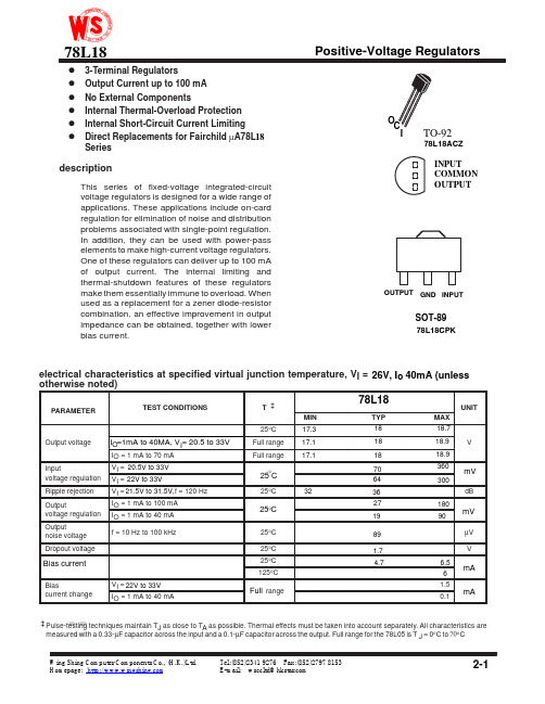
INPUT COMMON OUTPUT
OUTPUT GND INPUT
SOT-89
78L18CPK
electrical characteristics at specified virtual junction temperature, VI = 26V, I o 40mA (unless otherwise noted)
0
70
°C
Pad Location 78L18
90um
3
85um
90um
2
90um
9 9
95um
1
100um
Chip size 1.0 x 1.2 mm
Pad N 1 2 3
Pad Name Ground Input Output
X (um)
95 820 535
Y (um)
100 1010 1015
I
1 mA to 40 mA At A
Full range Full range 25°C 25 C 25°C 25°C 25 C 25°C 25°C 25°C 125°C
LM78L15ACMX中文资料
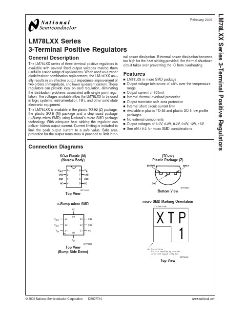
LM78LXX Series3-Terminal Positive RegulatorsGeneral DescriptionThe LM78LXX series of three terminal positive regulators isavailable with several fixed output voltages making themuseful in a wide range of applications.When used as a zenerdiode/resistor combination replacement,the LM78LXX usu-ally results in an effective output impedance improvement oftwo orders of magnitude,and lower quiescent current.Theseregulators can provide local on card regulation,eliminatingthe distribution problems associated with single point regu-lation.The voltages available allow the LM78LXX to be usedin logic systems,instrumentation,HiFi,and other solid stateelectronic equipment.The LM78LXX is available in the plastic TO-92(Z)package,the plastic SO-8(M)package and a chip sized package(8-Bump micro SMD)using National’s micro SMD packagetechnology.With adequate heat sinking the regulator candeliver100mA output current.Current limiting is included tolimit the peak output current to a safe value.Safe areaprotection for the output transistors is provided to limit inter-nal power dissipation.If internal power dissipation becomestoo high for the heat sinking provided,the thermal shutdowncircuit takes over preventing the IC from overheating.Featuresn LM78L05in micro SMD packagen Output voltage tolerances of±5%over the temperaturerangen Output current of100mAn Internal thermal overload protectionn Output transistor safe area protectionn Internal short circuit current limitn Available in plastic TO-92and plastic SO-8low profilepackagesn No external componentsn Output voltages of5.0V,6.2V,8.2V,9.0V,12V,15Vn See AN-1112for micro SMD considerations Connection DiagramsSO-8Plastic(M)(Narrow Body)00774402Top View8-Bump micro SMD00774424Top View(Bump Side Down)(TO-92)Plastic Package(Z)00774403Bottom Viewmicro SMD Marking Orientation00774433Top ViewFebruary2005LM78LXXSeries3-TerminalPositiveRegulators ©2005National Semiconductor Corporation Ordering InformationPackageOrder Number Output VoltageNSC Drawing Supplied As microSMDLM78L05IBP5V BPA08AAB Reel of 250LM78L05IBPX 5V BPA08AAB Reel of 3000LM78L09ITP 9V TPA08AAA Reel of 250LM78L09ITPX9V TPA08AAA Reel of 3000SOIC NarrowLM78L05ACM 5V M08A Rail of 95LM78L05ACMX 5V M08A Reel of 2500LM78L12ACM 12V M08A Rail of 95LM78L12ACMX 12V M08A Reel of 2500LM78L15ACM 15V M08A Rail of 95LM78L15ACMX15V M08A Reel of 2500TO-92LM78L05ACZ 5V Z03A Box of 1800LM78L62ACZ 6.2V Z03A Box of 1800LM78L82ACZ 8.2V Z03A Box of 1800LM78L09ACZ 9V Z03A Box of 1800LM78L12ACZ 12V Z03A Box of 1800LM78L15ACZ15VZ03ABox of 1800L M 78L X X S e r i e s 2Absolute Maximum Ratings (Note 1)If Military/Aerospace specified devices are required,please contact the National Semiconductor Sales Office/Distributors for availability and specifications.Power Dissipation (Note 5)Internally LimitedInput Voltage 35VStorage Temperature −65˚C to +150˚CESD Susceptibility (Note 2)1kVOperating Junction Temperature SO-8,TO-920˚C to 125˚C micro SMD −40˚C to 85˚CSoldering InformationInfrared or Convection (20sec.)235˚CWave Soldering (10sec.)260˚C (lead time)LM78LXX Electrical CharacteristicsLimits in standard typeface are for T J =25˚C,Bold typefaceapplies over 0˚C to 125˚C for SO-8and TO-92packages,and −40˚C to 85˚C for micro SMD package.Limits are guaran-teed by production testing or correlation techniques using standard Statistical Quality Control (SQC)methods.Unless other-wise specified:I O =40mA,C I =0.33µF,C O =0.1µF.LM78L05Unless otherwise specified,V IN =10V Symbol ParameterConditionsMin Typ Max UnitsV OOutput Voltage4.855.2V7V ≤V IN ≤20V 1mA ≤I O ≤40mA (Note 3)4.755.251mA ≤I O ≤70mA (Note 3)4.755.25∆V O Line Regulation 7V ≤V IN ≤20V 1875mV8V ≤V IN ≤20V 1054∆V O Load Regulation 1mA ≤I O ≤100mA 20601mA ≤I O ≤40mA530I Q Quiescent Current 35mA ∆I Q Quiescent Current Change 8V ≤V IN ≤20V 1.01mA ≤I O ≤40mA 0.1V nOutput Noise Voltage f =10Hz to 100kHz (Note 4)40µV Ripple Rejectionf =120Hz8V ≤V IN ≤16V4762dB I PKPeak Output Current140mA Average Output Voltage TempcoI O =5mA−0.65mV/˚C V IN (Min)Minimum Value of Input VoltageRequired to Maintain Line Regulation 6.77V θJAThermal Resistance (8-Bump micro SMD)230.9˚C/W LM78L62ACUnless otherwise specified,V IN =12V Symbol ParameterConditionsMin Typ Max UnitsV OOutput Voltage5.956.26.45V8.5V ≤V IN ≤20V 1mA ≤I O ≤40mA (Note 3)5.96.51mA ≤I O ≤70mA (Note 3)5.96.5LM78LXX Series3LM78LXX Electrical Characteristics Limits in standard typeface are for T J =25˚C,Bold typefaceapplies over 0˚C to 125˚C for SO-8and TO-92packages,and −40˚C to 85˚C for micro SMD package.Limits areguaranteed by production testing or correlation techniques using standard Statistical Quality Control (SQC)methods.Unless otherwise specified:I O =40mA,C I =0.33µF,C O =0.1µF.(Continued)LM78L62AC(Continued)Unless otherwise specified,V IN =12VSymbol ParameterConditions MinTyp Max Units∆V O Line Regulation 8.5V ≤V IN ≤20V 65175mV 9V ≤V IN ≤20V 55125∆V O Load Regulation 1mA ≤I O ≤100mA 13801mA ≤I O ≤40mA640I Q Quiescent Current 25.5mA ∆I Q Quiescent Current Change 8V ≤V IN ≤20V 1.51mA ≤I O ≤40mA 0.1V nOutput Noise Voltage f =10Hz to 100kHz (Note 4)50µV Ripple Rejectionf =120Hz10V ≤V IN ≤20V4046dB I PKPeak Output Current140mA Average Output Voltage TempcoI O =5mA−0.75mV/˚C V IN (Min)Minimum Value of Input VoltageRequired to Maintain Line Regulation7.9V LM78L82ACUnless otherwise specified,V IN =14V Symbol ParameterConditionsMin Typ Max UnitsV OOutput Voltage7.878.28.53V11V ≤V IN ≤23V 1mA ≤I O ≤40mA (Note 3)7.88.61mA ≤I O ≤70mA (Note 3)7.88.6∆V O Line Regulation 11V ≤V IN ≤23V 80175mV12V ≤V IN ≤23V 70125∆V O Load Regulation 1mA ≤I O ≤100mA 15801mA ≤I O ≤40mA840I Q Quiescent Current 25.5mA ∆I Q Quiescent Current Change 12V ≤V IN ≤23V 1.51mA ≤I O ≤40mA 0.1V nOutput Noise Voltage f =10Hz to 100kHz (Note 4)60µV Ripple Rejectionf =120Hz12V ≤V IN ≤22V3945dB I PKPeak Output Current140mA Average Output Voltage TempcoI O =5mA−0.8mV/˚C V IN (Min)Minimum Value of Input VoltageRequired to Maintain Line Regulation9.9V L M 78L X X S e r i e s 4LM78LXX Electrical Characteristics Limits in standard typeface are for T J =25˚C,Bold typefaceapplies over 0˚C to 125˚C for SO-8and TO-92packages,and −40˚C to 85˚C for micro SMD package.Limits areguaranteed by production testing or correlation techniques using standard Statistical Quality Control (SQC)methods.Unless otherwise specified:I O =40mA,C I =0.33µF,C O =0.1µF.(Continued)LM78L09ACUnless otherwise specified,V IN =15V Symbol ParameterConditionsMin Typ Max UnitsV OOutput Voltage8.649.09.36V11.5V ≤V IN ≤24V 1mA ≤I O ≤40mA (Note 3)8.559.451mA ≤I O ≤70mA (Note 3)8.559.45∆V O Line Regulation 11.5V ≤V IN ≤24V 100200mV13V ≤V IN ≤24V 90150∆V O Load Regulation 1mA ≤I O ≤100mA 20901mA ≤I O ≤40mA1045I Q Quiescent Current 25.5mA ∆I Q Quiescent Current Change 11.5V ≤V IN ≤24V 1.51mA ≤I O ≤40mA0.1V nOutput Noise Voltage 70µV Ripple Rejectionf =120Hz15V ≤V IN ≤25V3844dB I PKPeak Output Current140mA Average Output Voltage TempcoI O =5mA−0.9mV/˚C V IN (Min)Minimum Value of Input VoltageRequired to Maintain Line Regulation10.7V LM78L12ACUnless otherwise specified,V IN =19V Symbol ParameterConditionsMin Typ Max UnitsV OOutput Voltage11.51212.5V14.5V ≤V IN ≤27V 1mA ≤I O ≤40mA (Note 3)11.412.61mA ≤I O ≤70mA (Note 3)11.412.6∆V O Line Regulation 14.5V ≤V IN ≤27V 30180mV16V ≤V IN ≤27V 20110∆V O Load Regulation 1mA ≤I O ≤100mA 301001mA ≤I O ≤40mA1050I Q Quiescent Current 35mA ∆I Q Quiescent Current Change 16V ≤V IN ≤27V 11mA ≤I O ≤40mA0.1V nOutput Noise Voltage 80µV Ripple Rejectionf =120Hz15V ≤V IN ≤254054dB I PKPeak Output Current140mA Average Output Voltage TempcoI O =5mA−1.0mV/˚C LM78LXX Series5LM78LXX Electrical Characteristics Limits in standard typeface are for T J =25˚C,Bold typefaceapplies over 0˚C to 125˚C for SO-8and TO-92packages,and −40˚C to 85˚C for micro SMD package.Limits areguaranteed by production testing or correlation techniques using standard Statistical Quality Control (SQC)methods.Unless otherwise specified:I O =40mA,C I =0.33µF,C O =0.1µF.(Continued)LM78L12AC(Continued)Unless otherwise specified,V IN =19VSymbol ParameterConditionsMinTyp Max Units V IN (Min)Minimum Value of Input VoltageRequired to Maintain Line Regulation13.714.5VLM78L15ACUnless otherwise specified,V IN =23V Symbol ParameterConditionsMin Typ Max UnitsV OOutput Voltage14.415.015.6V17.5V ≤V IN ≤30V 1mA ≤I O ≤40mA (Note 3)14.2515.751mA ≤I O ≤70mA (Note 3)14.2515.75∆V O Line Regulation 17.5V ≤V IN ≤30V 37250mV20V ≤V IN ≤30V 25140∆V O Load Regulation 1mA ≤I O ≤100mA 351501mA ≤I O ≤40mA1275I QQuiescent Current 35mA ∆I QQuiescent Current Change 20V ≤V IN ≤30V 11mA ≤I O ≤40mA0.1V nOutput Noise Voltage 90µV Ripple Rejectionf =120Hz18.5V ≤V IN ≤28.5V3751dB I PKPeak Output Current140mA Average Output Voltage TempcoI O =5mA−1.3mV/˚C V IN (Min)Minimum Value of Input VoltageRequired to Maintain Line Regulation16.717.5V Note 1:Absolute Maximum Ratings indicate limits beyond which damage to the device may occur.Electrical specifications do not apply when operating the device outside of its stated operating conditions.Note 2:Human body model,1.5k Ωin series with 100pF.Note 3:Power dissipation ≤0.75W.Note 4:Recommended minimum load capacitance of 0.01µF to limit high frequency noise.Note 5:Typical thermal resistance values for the packages are:Z Package:θJC =60˚C/W,=θJA =230˚C/W M Package:θJA =180˚C/Wmicro SMD Package:θJA =230.9˚C/WL M 78L X X S e r i e s 6Typical Performance CharacteristicsMaximum Average Power Dissipation (Z Package)Peak Output Current0077441400774416Dropout Voltage Ripple Rejection0077441700774418Output Impedance Quiescent Current0077441900774420LM78LXX Series7Typical Performance Characteristics(Continued)Quiescent Current00774421Equivalent CircuitLM78LXX00774407L M 78L X X S e r i e s 8Typical ApplicationsFixed Output Regulator00774408*Required if the regulator is located more than 3"from the power supply filter.**See (Note 4)in the electrical characteristics table.Adjustable Output Regulator00774409V OUT =5V +(5V/R1+I Q )R25V/R1>3I Q ,load regulation (L r )≈[(R1+R2)/R1](L r of LM78L05)Current Regulator00774410I OUT =(V OUT /R1)+I Q>I Q =1.5mA over line and load changes5V,500mA Regulator with Short Circuit Protection00774411*Solid tantalum.**Heat sink Q1.***Optional:Improves ripple rejection and transient response.Load Regulation:0.6%0≤I L ≤250mA pulsed with t ON =50ms.LM78LXX Series9Typical Applications(Continued)±15V,100mA Dual Power Supply00774412*Solid tantalum.Variable Output Regulator 0.5V-18V00774413*Solid tantalum.V OUT =V G +5V,R1=(−V IN /I Q LM78L05)V OUT =5V (R2/R4)for (R2+R3)=(R4+R5)A 0.5V output will correspond to (R2/R4)=0.1(R3/R4)=0.9L M 78L X X S e r i e s 10Physical Dimensions inches(millimeters)unless otherwise notedNOTES:UNLESS OTHERWISE SPECIFIED1.EPOXY COATING2.63Sn/37Pb EUTECTIC BUMP3.RECOMMEND NON-SOLDER MASK DEFINED LANDING PAD.4.PIN A1IS ESTABLISHED BY LOWER LEFT CORNER WITH RESPECT TO TEXT ORIENTATION.REMAINING PINS ARE NUMBERED COUNTERCLOCKWISE.5.XXX IN DRAWING NUMBER REPRESENTS PACKAGE SIZE VARIATION WHERE X1IS PACKAGE WIDTH,X2IS PACKAGE LENGTH AND X3IS PACKAGE HEIGHT.6.REFERENCE JEDEC REGISTRATION MO-211,VARIATION BC.8-Bump micro SMD for LM78L05IBP OnlyNS Package Number BPA08AABX1=1.285mm X2=1.285mm X3=0.850mm LM78LXX Series 11Physical Dimensionsinches (millimeters)unless otherwise noted (Continued)8-Bump micro SMD for LM78L09ITP OnlyNS Package Number TPA08AAAX1=1.285mm X2=1.285mm X3=0.500mmL M 78L X X S e r i e s 12Physical Dimensions inches(millimeters)unless otherwise noted(Continued)S.O.Package(M)NS Package Number M08ALM78LXXSeries 13Physical Dimensionsinches (millimeters)unless otherwise noted (Continued)Molded Offset TO-92(Z)NS Package Number Z03ANational does not assume any responsibility for use of any circuitry described,no circuit patent licenses are implied and National reserves the right at any time without notice to change said circuitry and specifications.For the most current product information visit us at .LIFE SUPPORT POLICYNATIONAL’S PRODUCTS ARE NOT AUTHORIZED FOR USE AS CRITICAL COMPONENTS IN LIFE SUPPORT DEVICES OR SYSTEMS WITHOUT THE EXPRESS WRITTEN APPROVAL OF THE PRESIDENT AND GENERAL COUNSEL OF NATIONAL SEMICONDUCTOR CORPORATION.As used herein:1.Life support devices or systems are devices or systems which,(a)are intended for surgical implant into the body,or (b)support or sustain life,and whose failure to perform when properly used in accordance with instructions for use provided in the labeling,can be reasonably expected to result in a significant injury to the user.2.A critical component is any component of a life support device or system whose failure to perform can be reasonably expected to cause the failure of the life support device or system,or to affect its safety or effectiveness.BANNED SUBSTANCE COMPLIANCENational Semiconductor manufactures products and uses packing materials that meet the provisions of the Customer Products Stewardship Specification (CSP-9-111C2)and the Banned Substances and Materials of Interest Specification (CSP-9-111S2)and contain no ‘‘Banned Substances’’as defined in CSP-9-111S2.National Semiconductor Americas Customer Support CenterEmail:new.feedback@ Tel:1-800-272-9959National SemiconductorEurope Customer Support CenterFax:+49(0)180-5308586Email:europe.support@Deutsch Tel:+49(0)6995086208English Tel:+44(0)8702402171Français Tel:+33(0)141918790National Semiconductor Asia Pacific Customer Support CenterEmail:ap.support@National SemiconductorJapan Customer Support Center Fax:81-3-5639-7507Email:jpn.feedback@ Tel:81-3-5639-7560L M 78L X X S e r i e s 3-T e r m i n a l P o s i t i v e R e g u l a t o r s。
L78L05ABZ中文资料
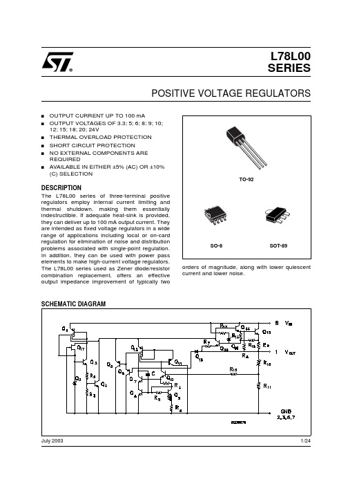
1/24July 2003s OUTPUT CURRENT UP TO 100mAsOUTPUT VOLTAGES OF 3.3;5;6;8;9;10;12;15;18;20;24Vs THERMAL OVERLOAD PROTECTION s SHORT CIRCUIT PROTECTIONsNO EXTERNAL COMPONENTS ARE REQUIREDsAVAILABLE IN EITHER ±5%(AC)OR ±10%(C)SELECTIONDESCRIPTIONThe L78L00series of three-terminal positive regulators employ internal current limiting and thermal shutdown,making them essentially indestructible.If adequate heat-sink is provided,they can deliver up to 100mA output current.They are intended as fixed voltage regulators in a wide range of applications including local or on-card regulation for elimination of noise and distribution problems associated with single-point regulation.In addition,they can be used with power pass elements to make high-current voltage regulators.The L78L00series used as Zener diode/resistor combination replacement,offers an effective output impedance improvement of typically twoorders of magnitude,along with lower quiescent current and lower noise.L78L00SERIESPOSITIVE VOLTAGEREGULATORSL78L00SERIES2/24ABSOLUTE MAXIMUM RATINGS(*)Our SO-8package used for Voltage Regulators is modified internally to have pins 2,3,6and 7electrically communed to the die attach flag.This particular frame decreases the total thermal resistance of the package and increasesits ability to dissipate power when an appro-priate area of copper on the printed circuit board is available for heat-sinking.The external dimensions are the same as for the standard SO-8.THERMAL DATA(*)Considering 6cm of copper Board heat-sinkTEST CIRCUITSCONNECTION DIAGRAM (top view)SymbolParameter²Value UnitV I DC Input VoltageV O =3.3to 9V 30V V O =12to 15V 35V O =18to 24V40I O Output Current 100mA P tot Power DissipationInternally Limited (*)T stg Storage Temperature Range-40to 150°C T opOperating Junction Temperature Range for L78L00C,L78L00AC 0to 125°C for L78L00AB-40to 125Symbol ParameterSO-8TO-92SOT-89Unit R thj-case Thermal Resistance Junction-case Max 2015°C/W R thj-ambThermal Resistance Junction-ambientMax55(*)200°C/WL78L00SERIES ORDERING CODESTYPE SO-8(TUBE)*TO-92(TUBE)**SOT-89(T&R)OUTPUT VOLTAGE L78L33C L78L33CD L78L33CZ 3.3VL78L33AC L78L33ACD L78L33ACZ L78L33ACUTR 3.3VL78L33AB L78L33ABD L78L33ABZ L78L33ABUTR 3.3VL78L05C L78L05CD L78L05CZ5VL78L05AC L78L05ACD L78L05ACZ L78L05ACUTR5VL78L05AB L78L05ABD L78L05ABZ L78L05ABUTR5VL78L06C L78L06CD L78L06CZ6VL78L06AC L78L06ACD L78L06ACZ L78L06ACUTR6VL78L06AB L78L06ABD L78L06ABZ L78L06ABUTR6VL78L08C L78L08CD L78L08CZ8VL78L08AC L78L08ACD L78L08ACZ L78L08ACUTR8VL78L08AB L78L08ABD L78L08ABZ L78L08ABUTR8VL78L09C L78L09CD L78L09CZ9VL78L09AC L78L09ACD L78L09ACZ L78L09ACUTR9VL78L09AB L78L09ABD L78L09ABZ L78L09ABUTR9VL78L10C L78L10CD L78L10CZ10VL78L10AC L78L10ACD L78L10ACZ L78L10ACUTR10VL78L10AB L78L10ABD L78L10ABZ L78L10ABUTR10VL78L12C L78L12CD L78L12CZ12VL78L12AC L78L12ACD L78L12ACZ L78L12ACUTR12VL78L12AB L78L12ABD L78L12ABZ L78L12ABUTR12VL78L15C L78L15CD L78L15CZ15VL78L15AC L78L15ACD L78L15ACZ L78L15ACUTR15VL78L15AB L78L15ABD L78L15ABZ L78L15ABUTR15VL78L18C L78L18CD L78L18CZ18VL78L18AC L78L18ACD L78L18ACZ L78L18ACUTR18VL78L18AB L78L18ABD L78L18ABZ L78L18ABUTR18VL78L20C L78L20CD L78L20CZ20VL78L20AC L78L20ACD L78L20ACZ L78L20ACUTR20VL78L20AB L78L20ABD L78L20ABZ L78L20ABUTR20VL78L24C L78L24CD L78L24CZ24VL78L24AC L78L24ACD L78L24ACZ L78L24ACUTR24VL78L24AB L78L24ABD L78L24ABZ L78L24ABUTR24V(*)Available in Tape&Reel with the suffix"13TR".(**)Available in Ammopak with the suffix"-AP"or in Tape&Reel with the suffix"TR".3/24L78L00SERIES4/24ELECTRICAL CHARACTERISTICS OF L78L33C (refer to the test circuits,T J =0to 125°C,V I =8.3V,I O =40mA,C I =0.33µF,C O =0.1µF unless otherwise specified)ELECTRICAL CHARACTERISTICS OF L78L05C (refer to the test circuits,T J =0to 125°C,V I =10V,I O =40mA,C I =0.33µF,C O =0.1µF unless otherwise specified).Symbol ParameterTest ConditionsMin.Typ.Max.Unit V O Output Voltage T J =25°C 3.036 3.33.564V V O Output Voltage I O =1to 40mA V I =5.3to 20V 2.97 3.63VI O =1to 70mA V I =8.3V2.973.63∆V O Line Regulation V I =5.3to 20V T J =25°C 150mV V I =6.3to 20V T J =25°C 100∆V O Load Regulation I O =1to 100mA T J =25°C 60mV I O =1to 40mA T J =25°C30I d Quiescent Current T J =25°C 6mA T J =125°C 5.5mA ∆I d Quiescent Current Change I O =1to 40mA 0.2mA V I =6.3to 20V 1.5eN Output Noise Voltage B =10Hz to 100KHz T J =25°C40µV SVR Supply Voltage Rejection V I =6.3to 16.3V f =120Hz I O =40mAT J =25°C4149dB V dDropout Voltage1.7V Symbol ParameterTest ConditionsMin.Typ.Max.Unit V O Output Voltage T J =25°C 4.655.4V V O Output Voltage I O =1to 40mA V I =7to 20V 4.5 5.5VI O =1to 70mA V I =10V4.55.5∆V O Line Regulation V I =8.5to 20V T J =25°C 200mV V I =9to 20V T J =25°C 150∆V O Load Regulation I O =1to 100mA T J =25°C 60mV I O =1to 40mA T J =25°C30I d Quiescent Current T J =25°C 6mA T J =125°C 5.5mA ∆I d Quiescent Current Change I O =1to 40mA 0.2mA V I =8to 20V 1.5eN Output Noise Voltage B =10Hz to 100KHz T J =25°C40µV SVR Supply Voltage Rejection V I =9to 20V f =120Hz I O =40mAT J =25°C4049dB V dDropout Voltage1.7VL78L00SERIES5/24ELECTRICAL CHARACTERISTICS OF L78L06C (refer to the test circuits,T J =0to 125°C,V I =12V,I O =40mA,C I =0.33µF,C O =0.1µF unless otherwise specified).ELECTRICAL CHARACTERISTICS OF L78L08C (refer to the test circuits,T J =0to 125°C,V I =14V,I O =40mA,C I =0.33µF,C O =0.1µF unless otherwise specified).Symbol ParameterTest ConditionsMin.Typ.Max.Unit V O Output Voltage T J =25°C 5.5266.48V V O Output Voltage I O =1to 40mA V I =8.5to 20V 5.4 6.6VI O =1to 70mA V I =12V5.46.6∆V O Line Regulation V I =8.5to 20V T J =25°C 200mV V I =9to 20V T J =25°C 150∆V O Load Regulation I O =1to 100mA T J =25°C 60mV I O =1to 40mA T J =25°C30I d Quiescent Current T J =25°C 6mA T J =125°C 5.5mA ∆I d Quiescent Current Change I O =1to 40mA 0.2mA V I =8to 20V 1.5eN Output Noise Voltage B =10Hz to 100KHz T J =25°C50µV SVR Supply Voltage Rejection V I =9to 20V f =120Hz I O =40mAT J =25°C3846dB V dDropout Voltage1.7V Symbol ParameterTest ConditionsMin.Typ.Max.Unit V O Output Voltage T J =25°C 7.3688.64V V O Output Voltage I O =1to 40mA V I =10.5to 23V 7.28.8VI O =1to 70mA V I =14V7.28.8∆V O Line Regulation V I =10.5to 23V T J =25°C 200mV V I =11to 23V T J =25°C 150∆V O Load Regulation I O =1to 100mA T J =25°C 80mV I O =1to 40mA T J =25°C40I d Quiescent Current T J =25°C 6mA T J =125°C 5.5mA ∆I d Quiescent Current Change I O =1to 40mA 0.2mA V I =11to 23V 1.5eN Output Noise Voltage B =10Hz to 100KHz T J =25°C60µV SVR Supply Voltage Rejection V I =12to 23V f =120Hz I O =40mAT J =25°C3645dB V dDropout Voltage1.7VL78L00SERIES6/24ELECTRICAL CHARACTERISTICS OF L78L09C (refer to the test circuits,T J =0to 125°C,V I =15V,I O =40mA,C I =0.33µF,C O =0.1µF unless otherwise specified).ELECTRICAL CHARACTERISTICS OF L78L10C (refer to the test circuits,T J =0to 125°C,V I =16V,I O =40mA,C I =0.33µF,C O =0.1µF unless otherwise specified).Symbol ParameterTest ConditionsMin.Typ.Max.Unit V O Output Voltage T J =25°C 8.2899.72V V O Output Voltage I O =1to 40mA V I =11.5to 23V 8.19.9VI O =1to 70mA V I =15V8.19.9∆V O Line Regulation V I =11.5to 23V T J =25°C 250mV V I =12to 23V T J =25°C 200∆V O Load Regulation I O =1to 100mA T J =25°C 80mV I O =1to 40mA T J =25°C40I d Quiescent Current T J =25°C 6mA T J =125°C 5.5mA ∆I d Quiescent Current Change I O =1to 40mA 0.2mA V I =12to 23V 1.5eN Output Noise Voltage B =10Hz to 100KHz T J =25°C70µV SVR Supply Voltage Rejection V I =12to 23V f =120Hz I O =40mAT J =25°C3644dB V dDropout Voltage1.7V Symbol ParameterTest ConditionsMin.Typ.Max.Unit V O Output Voltage T J =25°C 9.21010.8V V O Output Voltage I O =1to 40mA V I =12.5to 23V 911VI O =1to 70mA V I =16V911∆V O Line Regulation V I =12.5to 23V T J =25°C 230mV V I =13to 23V T J =25°C 170∆V O Load Regulation I O =1to 100mA T J =25°C 80mV I O =1to 40mA T J =25°C40I d Quiescent Current T J =25°C 6mA T J =125°C 5.5mA ∆I d Quiescent Current Change I O =1to 40mA 0.1mA V I =13to 23V 1.5eN Output Noise Voltage B =10Hz to 100KHz T J =25°C60µV SVR Supply Voltage Rejection V I =14to 23V f =120Hz I O =40mAT J =25°C3745dB V dDropout Voltage1.7VL78L00SERIES7/24ELECTRICAL CHARACTERISTICS OF L78L12C (refer to the test circuits,T J =0to 125°C,V I =19V,I O =40mA,C I =0.33µF,C O =0.1µF unless otherwise specified).ELECTRICAL CHARACTERISTICS OF L78L15C (refer to the test circuits,T J =0to 125°C,V I =23V,I O =40mA,C I =0.33µF,C O =0.1µF unless otherwise specified).Symbol ParameterTest ConditionsMin.Typ.Max.Unit V O Output Voltage T J =25°C 11.11212.9V V O Output Voltage I O =1to 40mA V I =14.5to 27V 10.813.2VI O =1to 70mA V I =19V10.813.2∆V O Line Regulation V I =14.5to 27V T J =25°C 250mV V I =16to 27V T J =25°C 200∆V O Load Regulation I O =1to 100mA T J =25°C 100mV I O =1to 40mA T J =25°C50I d Quiescent Current T J =25°C 6.5mA T J =125°C 6mA ∆I d Quiescent Current Change I O =1to 40mA 0.2mA V I =16to 27V 1.5eN Output Noise Voltage B =10Hz to 100KHz T J =25°C80µV SVR Supply Voltage Rejection V I =15to 25V f =120Hz I O =40mAT J =25°C3642dB V dDropout Voltage1.7V Symbol ParameterTest ConditionsMin.Typ.Max.Unit V O Output Voltage T J =25°C 13.81516.2V V O Output Voltage I O =1to 40mA V I =17.5to 30V 13.516.5VI O =1to 70mA V I =23V13.516.5∆V O Line Regulation V I =17.5to 30V T J =25°C 300mV V I =20to 30V T J =25°C 250∆V O Load Regulation I O =1to 100mA T J =25°C 150mV I O =1to 40mA T J =25°C75I d Quiescent Current T J =25°C 6.5mA T J =125°C 6mA ∆I d Quiescent Current Change I O =1to 40mA 0.2mA V I =20to 30V 1.5eN Output Noise Voltage B =10Hz to 100KHzT J =25°C90µV SVR Supply Voltage Rejection V I =18.5to 28.5V f =120Hz I O =40mA T J =25°C3339dB V dDropout Voltage1.7VL78L00SERIES8/24ELECTRICAL CHARACTERISTICS OF L78L18C (refer to the test circuits,T J =0to 125°C,V I =27V,I O =40mA,C I =0.33µF,C O =0.1µF unless otherwise specified).ELECTRICAL CHARACTERISTICS OF L78L20C (refer to the test circuits,T J =0to 125°C,V I =29V,I O =40mA,C I =0.33µF,C O =0.1µF unless otherwise specified)Symbol ParameterTest ConditionsMin.Typ.Max.Unit V O Output Voltage T J =25°C 16.61819.4V V O Output Voltage I O =1to 40mA V I =22to 33V 16.219.8VI O =1to 70mA V I =27V16.219.8∆V O Line Regulation V I =22to 33V T J =25°C 320mV V I =22to 33V T J =25°C 270∆V O Load Regulation I O =1to 100mA T J =25°C 170mV I O =1to 40mA T J =25°C85I d Quiescent Current T J =25°C 6.5mA T J =125°C 6mA ∆I d Quiescent Current Change I O =1to 40mA 0.2mA V I =23to 33V 1.5eN Output Noise Voltage B =10Hz to 100KHz T J =25°C120µV SVR Supply Voltage Rejection V I =23to 33V f =120Hz I O =40mAT J =25°C3238dB V dDropout Voltage1.7V Symbol ParameterTest ConditionsMin.Typ.Max.Unit V O Output Voltage T J =25°C 18.42021.6V V O Output Voltage I O =1to 40mA V I =24to 33V 1822VI O =1to 70mA V I =29V1822∆V O Line Regulation V I =22.5to 34V T J =25°C 330mV V I =24to 34V T J =25°C 280∆V O Load Regulation I O =1to 100mA T J =25°C 180mV I O =1to 40mA T J =25°C90I d Quiescent Current T J =25°C 6.5mA T J =125°C 6mA ∆I d Quiescent Current Change I O =1to 40mA 0.2mA V I =25to 33V 1.5eN Output Noise Voltage B =10Hz to 100KHz T J =25°C120µV SVR Supply Voltage Rejection V I =25to 35V f =120Hz I O =40mAT J =25°C3138dB V dDropout Voltage1.7VL78L00SERIES9/24ELECTRICAL CHARACTERISTICS OF L78L24C (refer to the test circuits,T J =0to 125°C,V I =33V,I O =40mA,C I =0.33µF,C O =0.1µF unless otherwise specified).ELECTRICAL CHARACTERISTICS OF L78L33AB AND L78L33AC(refer to the test circuits,V I =8.3V,I O =40mA,C I =0.33µF,C O =0.1µF,T J =0to 125°C for L78L33AC,T J =-40to 125°C for L78L33AB,unless otherwise specified)Symbol ParameterTest ConditionsMin.Typ.Max.Unit V O Output Voltage T J =25°C 22.12425.9V V O Output Voltage I O =1to 40mA V I =27to 38V 21.626.4VI O =1to 70mA V I =33V21.626.4∆V O Line Regulation V I =27to 38V T J =25°C 350mV V I =28to 38V T J =25°C 300∆V O Load Regulation I O =1to 100mA T J =25°C 200mV I O =1to 40mA T J =25°C100I d Quiescent Current T J =25°C 6.5mA T J =125°C 6mA ∆I d Quiescent Current Change I O =1to 40mA 0.2mA V I =28to 38V 1.5eN Output Noise Voltage B =10Hz to 100KHz T J =25°C200µV SVR Supply Voltage Rejection V I =29to 35V f =120Hz I O =40mAT J =25°C3037dB V dDropout Voltage1.7V Symbol ParameterTest ConditionsMin.Typ.Max.Unit V O Output Voltage T J =25°C 3.168 3.33.432V V O Output Voltage I O =1to 40mA V I =5.3to 20V 3.135 3.465VI O =1to 70mA V I =8.3V3.1353.465∆V O Line Regulation V I =5.3to 20V T J =25°C 150mV V I =6.3to 20V T J =25°C 100∆V O Load Regulation I O =1to 100mA T J =25°C 60mV I O =1to 40mA T J =25°C30I d Quiescent Current T J =25°C 6mA T J =125°C 5.5mA ∆I d Quiescent Current Change I O =1to 40mA 0.1mA V I =6.3to 20V 1.5eN Output Noise Voltage B =10Hz to 100KHz T J =25°C40µV SVR Supply Voltage Rejection V I =6.3to 16.3V f =120Hz I O =40mAT J =25°C4149dB V dDropout Voltage1.7VL78L00SERIES10/24ELECTRICAL CHARACTERISTICS OF L78L05AB AND L78L05AC (refer to the test circuits,V I =10V,I O =40mA,C I =0.33µF,C O =0.1µF,T J =0to 125°C for L78L05AC,T J =-40to 125°C for L78L05AB,unless otherwise specified)ELECTRICAL CHARACTERISTICS OF L78L06AB AND L78L06AC (refer to the test circuits,V I =12V,I O =40mA,C I =0.33µF,C O =0.1µF,T J =0to 125°C for L78L06AC,T J =-40to 125°C for L78L06AB,unless otherwise specified)Symbol ParameterTest ConditionsMin.Typ.Max.Unit V O Output Voltage T J =25°C 4.855.2V V O Output Voltage I O =1to 40mA V I =7to 20V 4.75 5.25VI O =1to 70mA V I =10V4.755.25∆V O Line Regulation V I =7to 20V T J =25°C 150mV V I =8to 20V T J =25°C 100∆V O Load Regulation I O =1to 100mA T J =25°C 60mV I O =1to 40mA T J =25°C30I d Quiescent Current T J =25°C 6mA T J =125°C 5.5mA ∆I d Quiescent Current Change I O =1to 40mA 0.1mA V I =8to 20V 1.5eN Output Noise Voltage B =10Hz to 100KHz T J =25°C40µV SVR Supply Voltage Rejection V I =8to 18V f =120Hz I O =40mAT J =25°C4149dB V dDropout Voltage1.7V Symbol ParameterTest ConditionsMin.Typ.Max.Unit V O Output Voltage T J =25°C 5.7666.24V V O Output Voltage I O =1to 40mA V I =8.5to 20V 5.7 6.3VI O =1to 70mA V I =12V5.76.3∆V O Line Regulation V I =8.5to 20V T J =25°C 150mV V I =9to 20V T J =25°C 100∆V O Load Regulation I O =1to 100mA T J =25°C 60mV I O =1to 40mA T J =25°C30I d Quiescent Current T J =25°C 6mA T J =125°C 5.5mA ∆I d Quiescent Current Change I O =1to 40mA 0.1mA V I =9to 20V 1.5eN Output Noise Voltage B =10Hz to 100KHz T J =25°C50µV SVR Supply Voltage Rejection V I =9to 20V f =120Hz I O =40mAT J =25°C3946dB V dDropout Voltage1.7V11/24ELECTRICAL CHARACTERISTICS OF L78L08AB AND L78L08AC (refer to the test circuits,V I =14V,I O =40mA,C I =0.33µF,C O =0.1µF,T J =0to 125°C for L78L08AC,T J =-40to 125°C for L78L08AB,unless otherwise specified)ELECTRICAL CHARACTERISTICS OF L78L09AB AND L78L09AC (refer to the test circuits,V I =15V,I O =40mA,C I =0.33µF,C O =0.1µF,T J =0to 125°C for L78L09AC,T J =-40to 125°C for L78L09AB,unless otherwise specified)Symbol ParameterTest ConditionsMin.Typ.Max.Unit V O Output Voltage T J =25°C 7.6888.32V V O Output Voltage I O =1to 40mA V I =10.5to 23V 7.68.4VI O =1to 70mA V I =14V7.68.4∆V O Line Regulation V I =10.5to 23V T J =25°C 175mV V I =11to 23V T J =25°C 125∆V O Load Regulation I O =1to 100mA T J =25°C 80mV I O =1to 40mA T J =25°C40I d Quiescent Current T J =25°C 6mA T J =125°C 5.5mA ∆I d Quiescent Current Change I O =1to 40mA 0.1mA V I =11to 23V 1.5eN Output Noise Voltage B =10Hz to 100KHz T J =25°C60µV SVR Supply Voltage Rejection V I =12to 23V f =120Hz I O =40mAT J =25°C3745dB V dDropout Voltage1.7V Symbol ParameterTest ConditionsMin.Typ.Max.Unit V O Output Voltage T J =25°C 8.6499.36V V O Output Voltage I O =1to 40mA V I =11.5to 23V 8.559.45VI O =1to 70mA V I =15V8.559.45∆V O Line Regulation V I =11.5to 23V T J =25°C 225mV V I =12to 23V T J =25°C 150∆V O Load Regulation I O =1to 100mA T J =25°C 80mV I O =1to 40mA T J =25°C40I d Quiescent Current T J =25°C 6mA T J =125°C 5.5mA ∆I d Quiescent Current Change I O =1to 40mA 0.1mA V I =12to 23V 1.5eN Output Noise Voltage B =10Hz to 100KHz T J =25°C70µV SVR Supply Voltage Rejection V I =12to 23V f =120Hz I O =40mAT J =25°C3744dB V dDropout Voltage1.7V12/24ELECTRICAL CHARACTERISTICS OF L78L10AB AND L78L10AC (refer to the test circuits,V I =16V,I O =40mA,C I =0.33µF,C O =0.1µF,T J =0to 125°C for L78L10AC,T J =-40to 125°C for L78L10AB,unless otherwise specified)ELECTRICAL CHARACTERISTICS OF L78L12AB AND L78L12AC (refer to the test circuits,V I =19V,I O =40mA,C I =0.33µF,C O =0.1µF,T J =0to 125°C for L78L12AC,T J =-40to 125°C for L78L12AB,unless otherwise specified)Symbol ParameterTest ConditionsMin.Typ.Max.Unit V O Output Voltage T J =25°C 9.61010.4V V O Output Voltage I O =1to 40mA V I =12.5to 23V 9.510.5VI O =1to 70mA V I =16V9.510.5∆V O Line Regulation V I =12.5to 23V T J =25°C 230mV V I =13to 23V T J =25°C 170∆V O Load Regulation I O =1to 100mA T J =25°C 80mV I O =1to 40mA T J =25°C40I d Quiescent Current T J =25°C 6mA T J =125°C 5.5mA ∆I d Quiescent Current Change I O =1to 40mA 0.1mA V I =13to 23V 1.5eN Output Noise Voltage B =10Hz to 100KHz T J =25°C60µV SVR Supply Voltage Rejection V I =14to 23V f =120Hz I O =40mAT J =25°C3745dB V dDropout Voltage1.7V Symbol ParameterTest ConditionsMin.Typ.Max.Unit V O Output Voltage T J =25°C 11.51212.5V V O Output Voltage I O =1to 40mA V I =14.5to 27V 11.412.6VI O =1to 70mA V I =19V11.412.6∆V O Line Regulation V I =14.5to 27V T J =25°C 250mV V I =16to 27V T J =25°C 200∆V O Load Regulation I O =1to 100mA T J =25°C 100mV I O =1to 40mA T J =25°C50I d Quiescent Current T J =25°C 6.5mA T J =125°C 6mA ∆I d Quiescent Current Change I O =1to 40mA 0.1mA V I =16to 27V 1.5eN Output Noise Voltage B =10Hz to 100KHz T J =25°C80µV SVR Supply Voltage Rejection V I =15to 25V f =120Hz I O =40mAT J =25°C3742dB V dDropout Voltage1.7V13/24ELECTRICAL CHARACTERISTICS OF L78L15AB AND L78L15AC (refer to the test circuits,V I =19V,I O =40mA,C I =0.33µF,C O =0.1µF,T J =0to 125°C for L78L15AC,T J =-40to 125°C for L78L15AB,unless otherwise specified)ELECTRICAL CHARACTERISTICS OF L78L18AB AND L78L18AC(refer to the test circuits,V I =27V,I O =40mA,C I =0.33µF,C O =0.1µF,T J =0to 125°C for L78L18AC,T J =-40to 125°C for L78L18AB,unless otherwise specified)Symbol ParameterTest ConditionsMin.Typ.Max.Unit V O Output Voltage T J =25°C 14.41515.6V V O Output Voltage I O =1to 40mA V I =17.5to 30V 14.2515.75VI O =1to 70mA V I =23V14.2515.75∆V O Line Regulation V I =17.5to 30V T J =25°C 300mV V I =20to 30V T J =25°C 250∆V O Load Regulation I O =1to 100mA T J =25°C 150mV I O =1to 40mA T J =25°C75I d Quiescent Current T J =25°C 6.5mA T J =125°C 6mA ∆I d Quiescent Current Change I O =1to 40mA 0.1mA V I =20to 30V 1.5eN Output Noise Voltage B =10Hz to 100KHzT J =25°C90µV SVR Supply Voltage Rejection V I =18.5to 28.5V f =120Hz I O =40mA T J =25°C3439dB V dDropout Voltage1.7V Symbol ParameterTest ConditionsMin.Typ.Max.Unit V O Output Voltage T J =25°C 17.31818.7V V O Output Voltage I O =1to 40mA V I =22to 33V 17.118.9VI O =1to 70mA V I =27V17.118.9∆V O Line Regulation V I =22to 33V T J =25°C 320mV V I =22to 33V T J =25°C 270∆V O Load Regulation I O =1to 100mA T J =25°C 170mV I O =1to 40mA T J =25°C85I d Quiescent Current T J =25°C 6.5mA T J =125°C 6mA ∆I d Quiescent Current Change I O =1to 40mA 0.1mA V I =23to 33V 1.5eN Output Noise Voltage B =10Hz to 100KHz T J =25°C120µV SVR Supply Voltage Rejection V I =23to 33V f =120Hz I O =40mAT J =25°C3338dB V dDropout Voltage1.7V14/24ELECTRICAL CHARACTERISTICS OF L78L20AB AND L78L20AC (refer to the test circuits,V I =29V,I O =40mA,C I =0.33µF,C O =0.1µF,T J =0to 125°C for L78L20AC,T J =-40to 125°C for L78L20AB,unless otherwise specified)ELECTRICAL CHARACTERISTICS OF L78L24AB AND L78L24AC (refer to the test circuits,V I =27V,I O =40mA,C I =0.33µF,C O =0.1µF,T J =0to 125°C for L78L24AC,T J =-40to 125°C for L78L24AB,unless otherwise specified)Symbol ParameterTest ConditionsMin.Typ.Max.Unit V O Output Voltage T J =25°C 19.22020.8V V O Output Voltage I O =1to 40mA V I =24to 33V 1921VI O =1to 70mA V I =29V1921∆V O Line Regulation V I =22.5to 34V T J =25°C 330mV V I =24to 34V T J =25°C 280∆V O Load Regulation I O =1to 100mA T J =25°C 180mV I O =1to 40mA T J =25°C90I d Quiescent Current T J =25°C 6.5mA T J =125°C 6mA ∆I d Quiescent Current Change I O =1to 40mA 0.1mA V I =25to 33V 1.5eN Output Noise Voltage B =10Hz to 100KHz T J =25°C120µV SVR Supply Voltage Rejection V I =25to 35V f =120Hz I O =40mAT J =25°C3238dB V dDropout Voltage1.7V Symbol ParameterTest ConditionsMin.Typ.Max.Unit V O Output Voltage T J =25°C 232425V V O Output Voltage I O =1to 40mA V I =27to 38V 22.825.2VI O =1to 70mA V I =33V22.825.2∆V O Line Regulation V I =27to 38V T J =25°C 350mV V I =28to 38V T J =25°C 300∆V O Load Regulation I O =1to 100mA T J =25°C 200mV I O =1to 40mA T J =25°C100I d Quiescent Current T J =25°C 6.5mA T J =125°C 6mA ∆I d Quiescent Current Change I O =1to 40mA 0.1mA V I =28to 38V 1.5eN Output Noise Voltage B =10Hz to 100KHz T J =25°C200µV SVR Supply Voltage Rejection V I =23to 33V f =120Hz I O =40mAT J =25°C3137dB V dDropout Voltage1.7VFigure1:L78L05/12Output Voltage vs Ambient TemperatureFigure2:L78L05/12/24Load Characteristics Figure3:L78L05/12/24Thermal Shutdown Figure4:L78L05/12Quiescent Current vs Output CurrentFigure5:L78L05Quiescent Current vs Input VoltageFigure6:L78L05/12/24OutputCharacteristics15/24Figure7:L78L05/12/24Ripple Rejection Figure8:L78L05Dropout Characteristics Figure9:L78L00Series Short Circuit OutputCurrent16/2417/24TYPICAL APPLICATIONSTable 10:High Output Current Short Circuit ProtectedFigure 11:Edit Boost CircuitFigure 12:CurrentRegulatorFigure13:Adjustable OutputRegulator18/24Information furnished is believed to be accurate and reliable. However, STMicroelectronics assumes no responsibility for the consequences of use of such information nor for any infringement of patents or other rights of third parties which may result from its use. No license is granted by implication or otherwise under any patent or patent rights of STMicroelectronics. Specifications mentioned in this publication are subject to change without notice. This publication supersedes and replaces all information previously supplied. STMicroelectronics products are not authorized for use as critical components in life support devices or systems without express written approval of STMicroelectronics.© The ST logo is a registered trademark of STMicroelectronics© 2003 STMicroelectronics - Printed in Italy - All Rights ReservedSTMicroelectronics GROUP OF COMPANIESAustralia - Brazil - Canada - China - Finland - France - Germany - Hong Kong - India - Israel - Italy - Japan - Malaysia - Malta - Morocco Singapore - Spain - Sweden - Switzerland - United Kingdom - United States.© 24/24。
L78S12中文资料
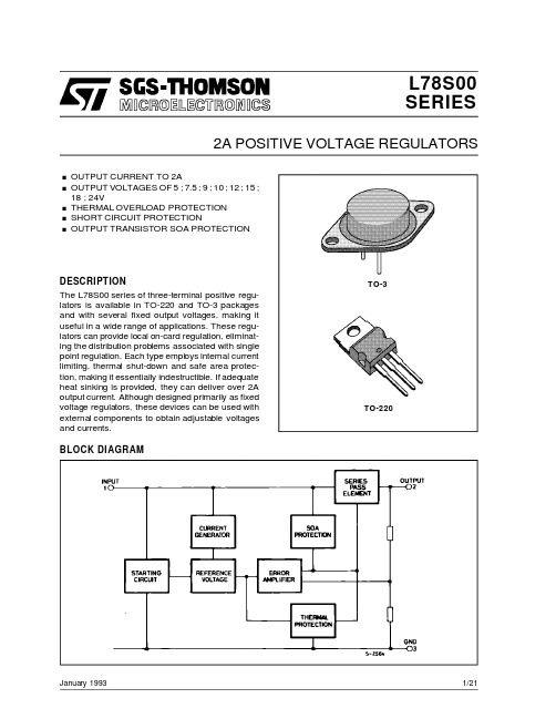
L78S00SERIESJanuary 19932A POSITIVE VOLTAGE REGULATORS.OUTPUT CURRENT TO 2A.OUTPUT VOLTAGES OF 5;7.5;9;10;12;15;18;24V.THERMAL OVERLOAD PROTECTION .SHORT CIRCUIT PROTECTION.OUTPUT TRANSISTOR SOA PROTECTIONDESCRIPTIONThe L78S00series of three-terminal positive regu-lators is available in TO-220and TO-3packages and with several fixed output voltages,making it useful in a wide range of applications.These regu-lators can provide local on-card regulation,eliminat-ing the distribution problems associated with single point regulation.Each type employs internal current limiting,thermal shut-down and safe area protec-tion,making it essentially indestructible.If adequate heat sinking is provided,they can deliver over 2A output current.Although designed primarily as fixed voltage regulators,these devices can be used with external components to obtain adjustable voltages and currents.TO-220BLOCK DIAGRAMTO-31/21ABSOLUTE MAXIMUM RATINGSSymbol Parameter Value UnitV i DC Input Voltage(for V o=5to18V)(for V o=24V)3540VVI o Output Current Internally limitedP t o t Power Dissipation Internally limitedT s t g Storage Temperature–65to+150°CT o p Operating Junction Temperature(for L78S00)(for L78S00C)–55to+1500to+150°C°CTHERMAL DATATO-220TO-3R t h j-cas e R t h j-amb Thermal Resistance Junction-caseThermal Resistance Junction-ambientMaxMax350435°C/W°C/WCONNECTION DIAGRAMS AND ORDERING NUMBERS(top views)Type T O-220T O-3Output Voltage L78S05L78S05C L78S75 L78S75C L78S09 L78S09C L78S10 L78S10C L78S12 L78S12C L78S15 L78S15C L78S18 L78S18C L78S24 L78S24C L78S05CVL78S75CVL78S09CVL78S10CVL78S12CVL78S15CVL78S18CVL78S24CVL78S05TL78S05CTL78S75TL78S75CTL78S09TL78S09CTL78S10TL78S10CTL78S12TL78S12CTL78S15TL78S15CTL78S18TL78S18CTL78S24TL78S24CT5V5V7.5V7.5V9V9V10V10V12V12V15V15V18V18V24V24VL78S00SERIES 2/21L78S00SERIES APPLICATION CIRCUITSCHEMATIC DIAGRAM3/21L78S00SERIESTEST CIRCUITSFigure1:DC Parameters.Figure2:Load Regulation. Figure3:Ripple Rejection.4/21ELECTRICAL CHARACTERISTICS FOR L78S05(refer to the test circuits,T j=25o C,V i=10V,I o=500mA unless otherwise specified)Symbol Parameter Test Conditions Min.Typ.Max.Unit V o Output Voltage 4.85 5.2V V o Output Voltage I o=1A V i=7V 4.755 5.25V∆V o Line Regulation V i=7to25VV i=8to25V 10050mVmV∆V o Load Regulation I o=20mA to2A100mVI d Quiescent Current8mA∆I d Quiescent Current Change I o=20mA to1A0.5mA ∆I d Quiescent Current Change I o=20mA V i=7to25V 1.3mA ∆V o∆TOutput Voltage Drift I o=5mA T j=-55to150o C-1.1mV/o Ce N Output Noise Voltage B=10Hz to100KHz40µVSVR Supply Voltage Rejection f=120Hz60dB V i Operating Input Voltage I o≤1.5A8V R o Output Resistance f=1KHz17mΩI sc Short Circuit Current V i=27V500mAI scp Short Circuit Peack Current3AELECTRICAL CHARACTERISTICS FOR L78S75(refer to the test circuits,T j=25o C,V i=12.5V,I o=500mA unless otherwise specified)Symbol Parameter Test Conditions Min.Typ.Max.Unit V o Output Voltage7.157.57.9V V o Output Voltage I o=1A V i=9.5V7.17.57.95V∆V o Line Regulation V i=9.5to25VV i=10.5to20V 12060mVmV∆V o Load Regulation I o=20mA to2A120mVI d Quiescent Current8mA∆I d Quiescent Current Change I o=20mA to1A0.5mA∆I d Quiescent Current Change I o=20mA V i=9.5to25V 1.3mA∆V o∆TOutput Voltage Drift I o=5mA T j=-55to150o C-0.8mV/o C e N Output Noise Voltage B=10Hz to100KHz52µV SVR Supply Voltage Rejection f=120Hz54dBV i Operating Input Voltage I o≤1.5A10.5VR o Output Resistance f=1KHz16mΩI sc Short Circuit Current V i=27V500mAI scp Short Circuit Peack Current3AL78S00SERIES5/21ELECTRICAL CHARACTERISTICS FOR L78S09(refer to the test circuits,T j=25o C,V i=14V,I o=500mA unless otherwise specified)Symbol Parameter Test Conditions Min.Typ.Max.Unit V o Output Voltage8.6599.35V V o Output Voltage I o=1A V i=11V8.699.4V∆V o Line Regulation V i=11to25VV i=11to20V 13065mVmV∆V o Load Regulation I o=20mA to2A130mVI d Quiescent Current8mA∆I d Quiescent Current Change I o=20mA to1A0.5mA ∆I d Quiescent Current Change I o=20mA V i=11to25V 1.3mA ∆V o∆TOutput Voltage Drift I o=5mA T j=-55to150o C-1mV/o Ce N Output Noise Voltage B=10Hz to100KHz60µVSVR Supply Voltage Rejection f=120Hz53dB V i Operating Input Voltage I o≤1.5A12V R o Output Resistance f=1KHz17mΩI sc Short Circuit Current V i=27V500mAI scp Short Circuit Peack Current3AELECTRICAL CHARACTERISTICS FOR L78S10(refer to the test circuits,T j=25o C,V i=15V,I o=500mA unless otherwise specified)Symbol Parameter Test Conditions Min.Typ.Max.Unit V o Output Voltage9.51010.5V V o Output Voltage I o=1A V i=12.5V9.41010.6V∆V o Line Regulation V i=12.5to30VV i=14to22V 200100mVmV∆V o Load Regulation I o=20mA to2A150mVI d Quiescent Current8mA∆I d Quiescent Current Change I o=20mA to1A0.5mA ∆I d Quiescent Current Change I o=20mA V i=12.5to30V1mA ∆V o∆TOutput Voltage Drift I o=5mA T j=-55to150o C-1mV/o Ce N Output Noise Voltage B=10Hz to100KHz65µVSVR Supply Voltage Rejection f=120Hz53dB V i Operating Input Voltage I o≤1.5A13V R o Output Resistance f=1KHz17mΩI sc Short Circuit Current V i=27V500mAI scp Short Circuit Peack Current3AL78S00SERIES6/21ELECTRICAL CHARACTERISTICS FOR L78S12(refer to the test circuits,T j=25o C,V i=19V,I o=500mA unless otherwise specified)Symbol Parameter Test Conditions Min.Typ.Max.Unit V o Output Voltage11.51212.5V V o Output Voltage I o=1A V i=14.5V11.41212.6V∆V o Line Regulation V i=14.5to30VV i=16to22V 240120mVmV∆V o Load Regulation I o=20mA to2A160mVI d Quiescent Current8mA∆I d Quiescent Current Change I o=20mA to1A0.5mA ∆I d Quiescent Current Change I o=20mA V i=14.5to30V1mA ∆V o∆TOutput Voltage Drift I o=5mA T j=-55to150o C-1mV/o Ce N Output Noise Voltage B=10Hz to100KHz75µVSVR Supply Voltage Rejection f=120Hz53dB V i Operating Input Voltage I o≤1.5A15V R o Output Resistance f=1KHz18mΩI sc Short Circuit Current V i=27V500mAI scp Short Circuit Peack Current3AELECTRICAL CHARACTERISTICS FOR L78S15(refer to the test circuits,T j=25o C,V i=23V,I o=500mA unless otherwise specified)Symbol Parameter Test Conditions Min.Typ.Max.Unit V o Output Voltage14.41515.6V V o Output Voltage I o=1A V i=17.5V14.251515.75V∆V o Line Regulation V i=17.5to30VV i=20to26V 300150mVmV∆V o Load Regulation I o=20mA to2A180mVI d Quiescent Current8mA∆I d Quiescent Current Change I o=20mA to1A0.5mA∆I d Quiescent Current Change I o=20mA V i=17.5to30V1mA∆V o∆TOutput Voltage Drift I o=5mA T j=-55to150o C-1mV/o C e N Output Noise Voltage B=10Hz to100KHz90µV SVR Supply Voltage Rejection f=120Hz52dBV i Operating Input Voltage I o≤1.5A18VR o Output Resistance f=1KHz19mΩI sc Short Circuit Current V i=27V500mAI scp Short Circuit Peack Current3AL78S00SERIES7/21ELECTRICAL CHARACTERISTICS FOR L78S18(refer to the test circuits,T j=25o C,V i=26V,I o=500mA unless otherwise specified)Symbol Parameter Test Conditions Min.Typ.Max.Unit V o Output Voltage17.11818.9V V o Output Voltage I o=1A V i=20.5V171819V∆V o Line Regulation V i=20.5to30VV i=22to28V 360180mVmV∆V o Load Regulation I o=20mA to2A200mVI d Quiescent Current8mA∆I d Quiescent Current Change I o=20mA to1A0.5mA ∆I d Quiescent Current Change I o=20mA V i=22to33V1mA ∆V o∆TOutput Voltage Drift I o=5mA T j=-55to150o C-1mV/o Ce N Output Noise Voltage B=10Hz to100KHz110µVSVR Supply Voltage Rejection f=120Hz49dB V i Operating Input Voltage I o≤1.5A21V R o Output Resistance f=1KHz22mΩI sc Short Circuit Current V i=27V500mAI scp Short Circuit Peack Current3AELECTRICAL CHARACTERISTICS FOR L78S24(refer to the test circuits,T j=25o C,V i=33V,I o=500mA unless otherwise specified)Symbol Parameter Test Conditions Min.Typ.Max.Unit V o Output Voltage232425V V o Output Voltage I o=1A V i=27V22.82425.2V∆V o Line Regulation V i=27to38VV i=30to36V 480240mVmV∆V o Load Regulation I o=20mA to2A250mVI d Quiescent Current8mA∆I d Quiescent Current Change I o=20mA to1A0.5mA ∆I d Quiescent Current Change I o=20mA V i=8to25V1mA ∆V o∆TOutput Voltage Drift I o=5mA T j=-55to150o C-1.5mV/o Ce N Output Noise Voltage B=10Hz to100KHz170µVSVR Supply Voltage Rejection f=120Hz48dB V i Operating Input Voltage I o≤1.5A27V R o Output Resistance f=1KHz23mΩI sc Short Circuit Current V i=27V500mAI scp Short Circuit Peack Current3AL78S00SERIES8/21ELECTRICAL CHARACTERISTICS FOR L78S05C(refer to the test circuits,T j=25o C,V i=10V,I o=500mA unless otherwise specified)Symbol Parameter Test Conditions Min.Typ.Max.Unit V o Output Voltage 4.85 5.2V V o Output Voltage I o=1A V i=7V 4.755 5.25V∆V o Line Regulation V i=7to25VV i=8to12V 10050mVmV∆V o Load Regulation I o=20mA to1.5AI o=2A80100mVI d Quiescent Current8mA∆I d Quiescent Current Change I o=20mA to1A0.5mA ∆I d Quiescent Current Change I o=20mA V i=7to25V 1.3mA ∆V o∆TOutput Voltage Drift I o=5mA T j=0to70o C-1.1mV/o Ce N Output Noise Voltage B=10Hz to100KHz40µVSVR Supply Voltage Rejection f=120Hz54dB V i Operating Input Voltage I o≤1.5A8V R o Output Resistance f=1KHz17mΩI sc Short Circuit Current V i=27V500mAI scp Short Circuit Peack Current3AELECTRICAL CHARACTERISTICS FOR L78S75C(refer to the test circuits,T j=25o C,V i=12.5V,I o=500mA unless otherwise specified)Symbol Parameter Test Conditions Min.Typ.Max.Unit V o Output Voltage7.157.57.9V V o Output Voltage I o=1A V i=9.5V7.17.57.95V∆V o Line Regulation V i=9.5to25VV i=10.5to20V 12060mVmV∆V o Load Regulation I o=20mA to1.5AI o=2A100140mVI d Quiescent Current8mA∆I d Quiescent Current Change I o=20mA to1A0.5mA∆I d Quiescent Current Change I o=20mA V i=9.5to25V 1.3mA∆V o∆TOutput Voltage Drift I o=5mA T j=0to70o C-0.8mV/o C e N Output Noise Voltage B=10Hz to100KHz52µV SVR Supply Voltage Rejection f=120Hz48dBV i Operating Input Voltage I o≤1.5A10.5VR o Output Resistance f=1KHz16mΩI sc Short Circuit Current V i=27V500mAI scp Short Circuit Peack Current3AL78S00SERIES9/21ELECTRICAL CHARACTERISTICS FOR L78S09C(refer to the test circuits,T j=25o C,V i=14V,I o=500mA unless otherwise specified)Symbol Parameter Test Conditions Min.Typ.Max.Unit V o Output Voltage8.6599.35V V o Output Voltage I o=1A V i=11V8.699.4V∆V o Line Regulation V i=11to25VV i=11to20V 13065mVmV∆V o Load Regulation I o=20mA to1.5AI o=2A100170mVI d Quiescent Current8mA∆I d Quiescent Current Change I o=20mA to1A0.5mA ∆I d Quiescent Current Change I o=20mA V i=11to25V 1.3mA ∆V o∆TOutput Voltage Drift I o=5mA T j=0to70o C-1mV/o Ce N Output Noise Voltage B=10Hz to100KHz60µVSVR Supply Voltage Rejection f=120Hz47dB V i Operating Input Voltage I o≤1.5A12V R o Output Resistance f=1KHz17mΩI sc Short Circuit Current V i=27V500mAI scp Short Circuit Peack Current3AELECTRICAL CHARACTERISTICS FOR L78S10C(refer to the test circuits,T j=25o C,V i=15V,I o=500mA unless otherwise specified)Symbol Parameter Test Conditions Min.Typ.Max.Unit V o Output Voltage9.51010.5V V o Output Voltage I o=1A V i=12.5V9.41010.6V∆V o Line Regulation V i=12.5to30VV i=14to22V 200100mVmV∆V o Load Regulation I o=20mA to1.5AI o=2A150240mVI d Quiescent Current8mA∆I d Quiescent Current Change I o=20mA to1A0.5mA ∆I d Quiescent Current Change I o=20mA V i=12.5to30V1mA ∆V o∆TOutput Voltage Drift I o=5mA T j=0to70o C-1mV/o Ce N Output Noise Voltage B=10Hz to100KHz65µVSVR Supply Voltage Rejection f=120Hz47dB V i Operating Input Voltage I o≤1.5A13V R o Output Resistance f=1KHz17mΩI sc Short Circuit Current V i=27V500mAI scp Short Circuit Peack Current3AL78S00SERIES10/21ELECTRICAL CHARACTERISTICS FOR L78S12C(refer to the test circuits,T j=25o C,V i=19V,I o=500mA unless otherwise specified)Symbol Parameter Test Conditions Min.Typ.Max.Unit V o Output Voltage11.51212.5V V o Output Voltage I o=1A V i=14.5V11.41212.6V∆V o Line Regulation V i=14.5to30VV i=16to22V 240120mVmV∆V o Load Regulation I o=20mA to1.5AI o=2A150240mVI d Quiescent Current8mA∆I d Quiescent Current Change I o=20mA to1A0.5mA ∆I d Quiescent Current Change I o=20mA V i=14.5to30V1mA ∆V o∆TOutput Voltage Drift I o=5mA T j=0to70o C-1mV/o Ce N Output Noise Voltage B=10Hz to100KHz75µVSVR Supply Voltage Rejection f=120Hz47dB V i Operating Input Voltage I o≤1.5A15V R o Output Resistance f=1KHz18mΩI sc Short Circuit Current V i=27V500mAI scp Short Circuit Peack Current3AELECTRICAL CHARACTERISTICS FOR L78S15C(refer to the test circuits,T j=25o C,V i=23V,I o=500mA unless otherwise specified)Symbol Parameter Test Conditions Min.Typ.Max.Unit V o Output Voltage14.41515.6V V o Output Voltage I o=1A V i=17.5V14.251515.75V∆V o Line Regulation V i=17.5to30VV i=20to26V 300150mVmV∆V o Load Regulation I o=20mA to1.5AI o=2A150300mV I d Quiescent Current8mA ∆I d Quiescent Current Change I o=20mA to1A0.5mA ∆I d Quiescent Current Change I o=20mA V i=17.5to30V1mA ∆V o∆TOutput Voltage Drift I o=5mA T j=0to70o C-1mV/o C e N Output Noise Voltage B=10Hz to100KHz90µV SVR Supply Voltage Rejection f=120Hz46dB V i Operating Input Voltage I o≤1.5A18V R o Output Resistance f=1KHz19mΩI sc Short Circuit Current V i=27V500mA I scp Short Circuit Peack Current3AELECTRICAL CHARACTERISTICS FOR L78S18C(refer to the test circuits,T j=25o C,V i=26V,I o=500mA unless otherwise specified)Symbol Parameter Test Conditions Min.Typ.Max.Unit V o Output Voltage17.11818.9V V o Output Voltage I o=1A V i=20.5V171819V∆V o Line Regulation V i=20.5to30VV i=22to28V 360180mVmV∆V o Load Regulation I o=20mA to1.5AI o=2A200360mVI d Quiescent Current8mA∆I d Quiescent Current Change I o=20mA to1A0.5mA ∆I d Quiescent Current Change I o=20mA V i=20.5to30V1mA ∆V o∆TOutput Voltage Drift I o=5mA T j=0to70o C-1mV/o Ce N Output Noise Voltage B=10Hz to100KHz110µVSVR Supply Voltage Rejection f=120Hz43dB V i Operating Input Voltage I o≤1.5A21V R o Output Resistance f=1KHz22mΩI sc Short Circuit Current V i=27V500mAI scp Short Circuit Peack Current3AELECTRICAL CHARACTERISTICS FOR L78S24C(refer to the test circuits,T j=25o C,V i=33V,I o=500mA unless otherwise specified)Symbol Parameter Test Conditions Min.Typ.Max.Unit V o Output Voltage232425V V o Output Voltage I o=1A V i=27V22.82425.2V∆V o Line Regulation V i=27to38VV i=30to36V 480240mVmV∆V o Load Regulation I o=20mA to1.5AI o=2A300480mV I d Quiescent Current8mA ∆I d Quiescent Current Change I o=20mA to1A0.5mA ∆I d Quiescent Current Change I o=20mA V i=27to38V1mA ∆V o∆TOutput Voltage Drift I o=5mA T j=0to70o C-1.5mV/o C e N Output Noise Voltage B=10Hz to100KHz170µV SVR Supply Voltage Rejection f=120Hz42dB V i Operating Input Voltage I o≤1.5A27V R o Output Resistance f=1KHz28mΩI sc Short Circuit Current V i=27V500mA I scp Short Circuit Peack Current3AFigure6:Supply Voltage Rejection vs.Frequen-cy.Figure7:Output Voltage vs.Junction Tempera-ture.Figure4:Dropout Voltage vs.Junction Tempera-ture.Figure5:Peak Output Current vs.Input/Output Differential Voltage.Figure8:Output Impedance vs.Frequency.Figure9:Quiescent Current vs.Junction Tempe-rature.Figure12:Quiescent Current vs.Input Voltage.Figure13:Fixed Output Regulator.Figure14:Constant Current Regulator. Figure10:Load Transient Response.Figure11:Line Transient Response.Notes:1.To specify an output voltage,substitute voltage value for”XX”.2.Although no output capacitor is needed for sta-bility,it does improve transient response.3.Required if regulator is located an appreciabledis-tance from power supply filter.V XXI O=+I dR1Figure 15:Circuit for Increasing Output Voltage.Figure 16:Adjustable Output Regulator(7to 30V).Figure 17:0.5to 10V Regulator.Figure 18:High Current Voltage Regulator.V BEQ 1R 1=I Q 1I REQ –βQ 1V BEQ 1I O =I REG +Q 1[I REG –]R 1R 4V O =V XXR 1I R1≥5I d R 2V 0=V XX (1+)+I d R 2R 1Figure 19:High Output Current with Short CircuitProtection.Figure 20:Tracking Voltage Regulator.V BEQ 2R SC =I SCFigure21:Positive and Negative Regulator.Figure22:Negative Output Voltage Circuit. (*)D1and D2are necessary if the load is connected be-tween+V0and–V0.Figure23:Switching Regulator.Figure24:High Input Voltage Circuit.V IN=V i–(V Z+V BE)Figure25:High Input Voltage Circuit.Figure26:High Output VoltageRegulator. V IN=V Z-V BEFigure 27:High Input and Output Voltage.Figure 28:Reducing Power Dissipation withDropping Resistor.V O =V XX +V Z1V i(min)–V XX –V DROP(max)R =I O(max)+I d(max)Figure 29:Remote Shuntdown.Figure 30:Power AM Modulator (unity voltagegain,Io ≤1A).Note :The circuit performs well up to 100KHz.Figure 31:Adjustable Output Voltage with Tem-perature Compensation.Note :Q 2is connected as a diode in order to compensatethe variati on of the Q 1V BE with the temperature.C allows a slow rise-time of the V OR 2V O =V XX (1+)+V BE R 1Figure32:Light Controllers(V o min=V xx+V BE).V O falls when the light goes up V O rises when the light goes up Figure33:Protection against Input Short-circuitwith High Capacitance Loads.Applications with high capacitance loads and anoutput voltage greater than6volts need an externaldiode(see fig.33)to protect the device against inputshort circuit.In this case the input voltage fallsrapidly while the output voltage decreases showly.The capacitance discharges by means of the Base-Emitter junction of the series pass transistor in theregulator.If the energy is sufficiently high,the tran-sistor may be destroyed.The external diode by-passes the current from the IC to ground.DIM.mm inchMIN.TYP.MAX.MIN.TYP.MAX. A11.0013.100.4330.516 B0.97 1.150.0380.045 C 1.50 1.650.0590.065 D8.328.920.3270.351 E19.0020.000.7480.787 G10.7011.100.4210.437 N16.5017.200.6490.677 P25.0026.000.984 1.023 R 4.00 4.090.1570.161 U38.5039.30 1.515 1.547 V30.0030.30 1.187 1.193CDN BVUR APEGOP003F TO-3MECHANICAL DATADIM.mminch MIN.TYP.MAX.MIN.TYP.MAX.A 4.40 4.600.1730.181C 1.23 1.320.0480.051D 2.402.720.0940.107D1 1.270.050E 0.490.700.0190.027F 0.610.880.0240.034F1 1.14 1.700.0440.067F2 1.14 1.700.0440.067G 4.95 5.150.1940.203G1 2.4 2.70.0940.106H210.010.400.3930.409L216.40.645L413.014.00.5110.551L5 2.65 2.950.1040.116L615.215.90.5980.625L7 6.2 6.60.2440.260L9 3.5 4.20.1370.165DIA.3.75 3.850.1470.151L6ACDED 1FGL7L2Dia.F 1L5L4H 2L9F 2G 1TO-220MECHANICAL DATAP011C元器件交易网L78S00SERIES Information furnished is believed to be accurate and reliable.However,SGS-THOMSON Microelectronics assumes no responsability for theconsequences of use of such information nor for any infringement of patents or other rights of third parties which may results from its use.Nolicense is granted by implication or otherwise under any patent or patent rights of SGS-THOMSON Microelectronics.Specificationsmentionedin this publication are subject to change without notice.This publication supersedes and replaces all information previously supplied.SGS-THOMSON Microelectronics products are not authorized for use ascritical components in life support devices or systems without expresswritten approval of SGS-THOMSON Microelectonics.©1994SGS-THOMSON Microelectronics-All Rights ReservedSGS-THOMSON Microelectronics GROUP OF COMPANIESAustralia-Brazil-France-Germany-Hong Kong-Italy-Japan-Korea-Malaysia-Malta-Morocco-The Netherlands-Singapore-Spain-Sweden-Switzerland-Taiwan-Thailand-United Kingdom-U.S.A21/21。
CYD36S18V18资料
FullFlex™ Synchronous SDR Dual-Port SRAMFullFlexFeatures•True dual-ported memory allows simultaneous access to the shared array from each port•Synchronous pipelined operation with Single Data Rate (SDR) operation on each port—SDR interface at 250 MHz—Up to 36-Gb/s bandwidth (250 MHz * 72 bit * 2 ports)•Selectable pipelined or flow-through mode•1.5V or 1.8V core power supply•Commercial and Industrial temperature•IEEE 1149.1 JTAG boundary scan•Available in 484-ball PBGA Packages and 256-ballFBGA packages•FullFlex72 family—36-Mbit: 512K x 72 (CYD36S72V18)—18-Mbit: 256K x 72 (CYD18S72V18)—9-Mbit: 128K x 72 (CYD09S72V18)—4-Mbit: 64K x 72 (CYD04S72V18)•FullFlex36 family—36-Mbit: 1M x 36 (CYD36S36V18)—18-Mbit: 512K x 36 (CYD18S36V18)—9-Mbit: 256K x 36 (CYD09S36V18)—4-Mbit: 128K x 36 (CYD04S36V18)•FullFlex18 family—36-Mbit: 2M x 18 (CYD36S18V18)—18-Mbit: 1M x 18 (CYD18S18V18)—9-Mbit: 512K x 18 (CYD09S18V18)—4-Mbit: 256K x 18 (CYD04S18V18)•Built-in deterministic access control to manageaddress collisions—Deterministic flag output upon collision detection —Collision detection on back-to-back clock cycles —First Busy Address readback•Advanced features for improved high-speed datatransfer and flexibility—Variable Impedance Matching (VIM)—Echo clocks—Selectable LVTTL (3.3V), Extended HSTL(1.4V–1.9V), 1.8V LVCMOS, or 2.5V LVCMOS I/O oneach port—Burst counters for sequential memory access—Mailbox with interrupt flags for message passing —Dual Chip Enables for easy depth expansion Functional DescriptionThe FullFlex™ Dual-Port SRAM families consist of 4-Mbit, 9-Mbit, 18-Mbit, and 36-Mbit synchronous, true dual-port static RAMs that are high-speed, low-power 1.8V/1.5V CMOS. Two ports are provided, allowing the array to be accessed simulta-neously. Simultaneous access to a location triggers determin-istic access control. For FullFlex72 these ports can operate independently with 72-bit bus widths and each port can be independently configured for two pipelined stages. Each port can also be configured to operate in pipelined or flow-through mode.Advanced features include built-in deterministic access control to manage address collisions during simultaneous access to the same memory location, Variable Impedance Matching (VIM) to improve data transmission by matching the output driver impedance to the line impedance, and echo clocks to improve data transfer.To reduce the static power consumption, chip enables can be used to power down the internal circuitry. The number of cycles of latency before a change in CE0 or CE1 will enable or disable the databus matches the number of cycles of read latency selected for the device. In order for a valid write or read to occur, both chip enable inputs on a port must be active. Each port contains an optional burst counter on the input address register. After externally loading the counter with the initial address, the counter will increment the address inter-nally.Additional features of this device include a mask register and a mirror register to control counter increments and wrap-around. The counter-interrupt (CNTINT) flags notify the host that the counter will reach maximum count value on the next clock cycle. The host can read the burst-counter internal address, mask register address, and busy address on the address lines. The host can also load the counter with the address stored in the mirror register by utilizing the retransmit functionality. Mailbox interrupt flags can be used for message passing, and JTAG boundary scan and asynchronous Master Reset (MRST) are also available. The logic block diagram in Figure1 displays these features.The FullFlex72 is offered in a 484-ball plastic BGA package. The FullFlex36 and FullFlex18 are offered in both 484-ball and 256-ball fine pitch BGA packages.Notes:1.The CYD36S18V18 device has 21 address bits. The CYD36S36V18 and the CYD18S18V18 devices have 20 address bits. The CYD36S72V18, CYD18S36V18, and the CYD09S18V18 devices have 19 address bits. The CYD18S72V18, CYD09S36V18, and the CYD04S18V18 devices have 18 address bits. The CYD09S72V18 and the CYD04S36V18 devices have 17 address bits. The CYD04S72V18 has 16 address bits.2.The FullFlex72 family of devices has 72 data lines. The FullFlex36 family of devices has 36 data lines. The FullFlex18 family of devices has 18 data lines.3.The FullFlex72 family of devices has eight byte enables. The FullFlex36 family of devices has four byte enables. The FullFlex18 family of devices has two byte enables.L PORTSTD[1:0]LDQ[71:0]L BE [7:0]L R/W L FTSEL RPORTSTD[1:0]RDQ [71:0]R BE [7:0]R CE0R CE1R OE R R/W R A [20:0]L CNT/MSK L ADS L CNTEN L CNTRST L RET L LC L LA [20:0]R CNT/MSK RADS R CNTEN R CNTRST R R CNTINT RC RWRP RCONFIG BlockCONFIG BlockIO Control IO ControlAddress &Counter LogicAddress &Counter LogicINT LTRST TMS TDI TDO TCK JTAGMRST READY R RREADY L LowSPD LRESET LOGICINT RBUSY LBUSY RMailboxesCollision Detection LogicDual Ported ArrayFigure 1. FullFlex72 18-Mbit (CYD18S72V18) Block Diagram [1, 2, 3]CQEN L CQEN R L CE1L OE L CQ1R CQ1R CQ0R CQ0RLCQ0L CQ1L CQ1L ZQ0R ZQ1R ZQ0L ZQ1LNotes:4.Leaving this pin NC disables VIM.5.Leave this ball unconnected for CYD18S72V18, CYD09S72V18 and CYD04S72V18.6.Leave this ball unconnected for CYD09S72V18 and CYD04S72V18.7.Leave this ball unconnected for CYD04S72V18.FullFlex72 SDR 484-ball BGA Pinout (Top View)12345678910111213141516171819202122A NCDQ61L DQ59L DQ57L DQ54L DQ51L DQ48L DQ45L DQ42L DQ39L DQ36L DQ36R DQ39R DQ42R DQ45R DQ48R DQ51R DQ54R DQ57R DQ59R DQ61RNCB DQ63L DQ62L DQ60L DQ58L DQ55L DQ52L DQ49L DQ46L DQ43L DQ40L DQ37L DQ37R DQ40R DQ43R DQ46R DQ49R DQ52R DQ55R DQ58R DQ60R DQ62R DQ63R C DQ65L DQ64L VSS VSS DQ56L DQ53L DQ50L DQ47L DQ44L DQ41L DQ38L DQ38R DQ41R DQ44R DQ47R DQ50R DQ53R DQ56R VSSVSS DQ64R DQ65R D DQ67L DQ66LVSS VSSVSS CQ1L CQ1L VSSLOW SPDL PORT STD0L ZQ0L [4]BUSY L CNTI NTL PORTSTD1LNCCQ1R CQ1R VSSVSSVSS DQ66R DQ67RE DQ69L DQ68L VDDI OL VSSVSS VDDI OL VDDI OL VDDI OL VDDI OL VDDI OL VTTL VTTL VTTL VDDI OR VDDI OR VDDI OR VDDIORNCVSS VDDI OR DQ68R DQ69RF DQ71L DQ70L CE1L CE0L VDDI OL VDDI OL VDDI OL VDDI OL VDDI OL VCO RE VCO RE VCO RE VCO RE VDDI OR VDDI OR VDDI OR VDDI OR VDDI OR CE0R CE1R DQ70R DQ71R G A0L A1L RETL BE4L VDDI OL VDDI OL VREF L VSSVSS VSS VSS VSS VSS VSS VSS VREF R VDDI OR VDDI OR BE4R RETR A1RA0R H A2L A3LWRP LBE5L VDDI OL VDDI OL VSS VSS VSS VSS VSS VSS VSS VSS VSS VSS VDDI OR VDDI OR BE5R WRPRA3RA2R J A4L A5L READ YL BE6L VDDI OL VDDI OL VSSVSS VSS VSS VSS VSS VSS VSS VSS VSS VDDI OR VDDI OR BE6R READ YR A5RA4R K A6L A7L ZQ1L [4]BE7L VTTL VCO RE VSS VSS VSS VSS VSS VSS VSS VSS VSS VSS VCO RE VDDI OR BE7R ZQ1R [4]A7RA6R L A8LA9LCLOEL VTTL VCOREVSS VSS VSS VSS VSS VSS VSS VSS VSS VSS VCO REVTTL OER CRA9RA8RM A10L A11LVSS BE3L VTTL VCORE VSS VSS VSS VSS VSS VSS VSS VSS VSS VSS VCO REVTTL BE3R VSS A11R A10R N A12L A13L ADSL BE2L VDDI OL VCOREVSSVSS VSS VSS VSS VSS VSS VSS VSS VSSVCO REVTTL BE2R ADSR A13R A12R P A14L A15L CNT/MSKL BE1L VDDI OL VDDI OL VSSVSSVSSVSSVSSVSSVSSVSSVSSVSS VDDI OR VDDI OR BE1R CNT/MSKR A15R A14RR A16L [7]A17L [6]CNTE NL BE0L VDDI OL VDDI OL VSSVSS VSS VSS VSS VSS VSS VSS VSSVSS VDDI OR VDDI OR BE0R CNTE NRA17R [6]A16R[7]T A18L[5]NCCNTR STL INTL VDDI OL VDDI OL VREF L VSSVSSVSSVSSVSSVSSVSSVSS VREF R VDDI OR VDDI OR INTR CNTRSTRNCA18R[5]U DQ35L DQ34L R/WL CQE NL VDDI OL VDDI OL VDDI OL VDDI OL VDDI OL VCO RE VCO RE VCO RE VCO RE VDDI OR VDDI OR VDDI OR VDDI OR VDDI OR CQE NR R/WR DQ34R DQ35R V DQ33L DQ32L FTSE LLVDDI OL NCVDDI OL VDDI OL VDDI OL VDDI OL VTTL VTTL VTTL VDDI OR VDDI OR VDDI OR VDDI OR VDDI OR TRST VDDI OR FTSE LRDQ32R DQ33R W DQ31L DQ30L VSS MRST VSS CQ0L CQ0LNCPORT STD1R CNTI NTR BUSY R ZQ0R [4]PORT STD0RLOW SPDR VSS CQ0R CQ0R VSSTDITDO DQ30R DQ31R Y DQ29L DQ28LVSS VSS DQ20L DQ17L DQ14L DQ11L DQ8L DQ5L DQ2L DQ2R DQ5R DQ8R DQ11R DQ14R DQ17R DQ20RTMSTCK DQ28R DQ29RAA DQ27L DQ26L DQ24L DQ22L DQ19L DQ16L DQ13L DQ10L DQ7L DQ4L DQ1L DQ1R DQ4R DQ7R DQ10R DQ13R DQ16R DQ19R DQ22R DQ24R DQ26R DQ27R ABNCDQ25L DQ23L DQ21L DQ18L DQ15L DQ12L DQ9L DQ6L DQ3L DQ0L DQ0R DQ3R DQ6R DQ9R DQ12R DQ15R DQ18R DQ21R DQ23R DQ25RNCFullFlex36 SDR 484-ball BGA Pinout (Top View)[8] 12345678910111213141516171819202122A NC NC NC NC NC DQ33LDQ30LDQ27LDQ24LDQ21LDQ18LDQ18RDQ21RDQ24RDQ27RDQ30RDQ33RNC NC NC NC NCB NC NC NC NC NC DQ34LDQ31LDQ28LDQ25LDQ22LDQ19LDQ19RDQ22RDQ25RDQ28RDQ31RDQ34RNC NC NC NC NCC NC NC VSS VSS NC DQ35LDQ32LDQ29LDQ26LDQ23LDQ20LDQ20RDQ23RDQ26RDQ29RDQ32RDQ35RNC VSS VSS NC NCD NC NC VSS VSS VSS CQ1L CQ1L VSS LOWSPDLPORTSTD0LZQ0L[4]BUSYLCNTINTLPORTSTD1LNC CQ1R CQ1R VSS VSS VSS NC NCE NC NC VDDIOLVSS VSS VDDIOLVDDIORVDDIORVDDIORVDDIORVTTL VTTL VTTL VDDIOLVDDIOLVDDIOLVDDIOLNC VSS VDDIORNC NCF NC NC CE1L CE0L VDDIOLVDDIOLVDDIORVDDIORVDDIORVCOREVCOREVCOREVCOREVDDIOLVDDIOLVDDIOLVDDIORVDDIORCE0R CE1R NC NCG A0L A1L RETL BE2L VDDIOLVDDIOLVREFLVSS VSS VSS VSS VSS VSS VSS VSS VREFRVDDIORVDDIORBE2R RETR A1R A0RH A2L A3L WRPLBE3L VDDIOLVDDIOLVSS VSS VSS VSS VSS VSS VSS VSS VSS VSS VDDIORVDDIORBE3R WRPRA3R A2RJ A4L A5L READYLNC VDDIOLVDDIOLVSS VSS VSS VSS VSS VSS VSS VSS VSS VSS VDDIORVDDIORNC READYRA5R A4RK A6L A7L ZQ1L[4]NC VTTL VCOREVSS VSS VSS VSS VSS VSS VSS VSS VSS VSS VCOREVDDIORNC ZQ1R[4]A7R A6RL A8L A9L CL OEL VTTL VCOREVSS VSS VSS VSS VSS VSS VSS VSS VSS VSS VCOREVTTL OER CR A9R A8RM A10L A11L VSS NC VTTL VCOREVSS VSS VSS VSS VSS VSS VSS VSS VSS VSS VCOREVTTL NC VSS A11R A10RN A12L A13L ADSL NC VDDIOLVCOREVSS VSS VSS VSS VSS VSS VSS VSS VSS VSS VCOREVTTL NC ADSR A13R A12RP A14L A15L CNT/MSKLBE1L VDDIOLVDDIOLVSS VSS VSS VSS VSS VSS VSS VSS VSS VSS VDDIORVDDIORBE1R CNT/MSKRA15R A14RR A16L A17L CNTENLBE0L VDDIOLVDDIOLVSS VSS VSS VSS VSS VSS VSS VSS VSS VSS VDDIORVDDIORBE0R CNTENRA17R A16RT A18L A19L CNTRSTLINTL VDDIOLVDDIOLVREFLVSS VSS VSS VSS VSS VSS VSS VSS VREFRVDDIORVDDIORINTR CNTRSTRA19R A18RU NC NC R/WL CQENLVDDIOLVDDIOLVDDIORVDDIORVDDIORVCOREVCOREVCOREVCOREVDDIOLVDDIOLVDDIOLVDDIORVDDIORCQENRR/WR NC NCV NC NC FTSELLVDDIOLNC VDDIORVDDIORVDDIORVDDIORVTTL VTTL VTTL VDDIOLVDDIOLVDDIOLVDDIOLVDDIORTRST VDDIORFTSELRNC NCW NC NC VSS MRST VSS CQ0L CQ0L NC PORTSTD1RCNTINTRBUSYRZQ0R[4]PORTSTD0RLOWSPDRVSS CQ0R CQ0R VSS TDI TDO NC NCY NC NC VSS VSS NC DQ17LDQ14LDQ11LDQ8L DQ5L DQ2L DQ2R DQ5R DQ8R DQ11RDQ14RDQ17RNC TMS TCK NC NCAA NC NC NC NC NC DQ16LDQ13LDQ10LDQ7L DQ4L DQ1L DQ1R DQ4R DQ7R DQ10RDQ13RDQ16RNC NC NC NC NCAB NC NC NC NC NC DQ15LDQ12LDQ9L DQ6L DQ3L DQ0L DQ0R DQ3R DQ6R DQ9R DQ12RDQ15RNC NC NC NC NCNote:e this pinout only for device CYD36S36V18 of the FullFlex36 family.FullFlex18 SDR 484-ball BGA Pinout (Top View)[9] 12345678910111213141516171819202122A NC NC NC NC NC NC NC NC DQ15LDQ12LDQ9L DQ9R DQ12RDQ15RNC NC NC NC NC NC NC NCB NC NC NC NC NC NC NC NC DQ16LDQ13LDQ10LDQ10RDQ13RDQ16RNC NC NC NC NC NC NC NCC NC NC VSS VSS NC NC NC NC DQ17LDQ14LDQ11LDQ11RDQ14RDQ17RNC NC NC NC VSS VSS NC NCD NC NC VSS VSS VSS CQ1L CQ1L VSS LOWSPDLPORTSTD0LZQ0L[4]BUSYLCNTINTLPORTSTD1LNC CQ1R CQ1R VSS VSS VSS NC NCE NC NC VDDIOLVSS VSS VDDIOLVDDIORVDDIORVDDIORVDDIORVTTL VTTL VTTL VDDIOLVDDIOLVDDIOLVDDIOLNC VSS VDDIORNC NCF NC NC CE1L CE0L VDDIOLVDDIOLVDDIORVDDIORVDDIORVCOREVCOREVCOREVCOREVDDIOLVDDIOLVDDIOLVDDIORVDDIORCE0R CE1R NC NCG A0L A1L RETL BE1L VDDIOLVDDIOLVREFLVSS VSS VSS VSS VSS VSS VSS VSS VREFRVDDIORVDDIORBE1R RETR A1R A0RH A2L A3L WRPLNC VDDIOLVDDIOLVSS VSS VSS VSS VSS VSS VSS VSS VSS VSS VDDIORVDDIORNC WRPRA3R A2RJ A4L A5L READYLNC VDDIOLVDDIOLVSS VSS VSS VSS VSS VSS VSS VSS VSS VSS VDDIORVDDIORNC READYRA5R A4RK A6L A7L ZQ1L[4]NC VTTL VCOREVSS VSS VSS VSS VSS VSS VSS VSS VSS VSS VCOREVDDIORNC ZQ1R[4]A7R A6RL A8L A9L CL OEL VTTL VCOREVSS VSS VSS VSS VSS VSS VSS VSS VSS VSS VCOREVTTL OER CR A9R A8RM A10L A11L VSS NC VTTL VCOREVSS VSS VSS VSS VSS VSS VSS VSS VSS VSS VCOREVTTL NC VSS A11R A10RN A12L A13L ADSL NC VDDIOLVCOREVSS VSS VSS VSS VSS VSS VSS VSS VSS VSS VCOREVTTL NC ADSR A13R A12RP A14L A15L CNT/MSKLNC VDDIOLVDDIOLVSS VSS VSS VSS VSS VSS VSS VSS VSS VSS VDDIORVDDIORNC CNT/MSKRA15R A14RR A16L A17L CNTENLBE0L VDDIOLVDDIOLVSS VSS VSS VSS VSS VSS VSS VSS VSS VSS VDDIORVDDIORBE0R CNTENRA17R A16RT A18L A19L CNTRSTLINTL VDDIOLVDDIOLVREFLVSS VSS VSS VSS VSS VSS VSS VSS VREFRVDDIORVDDIORINTR CNTRSTRA19R A18RU A20L NC R/WL CQENLVDDIOLVDDIOLVDDIORVDDIORVDDIORVCOREVCOREVCOREVCOREVDDIOLVDDIOLVDDIOLVDDIORVDDIORCQENRR/WR NC A20RV NC NC FTSELLVDDIOLNC VDDIORVDDIORVDDIORVDDIORVTTL VTTL VTTL VDDIOLVDDIOLVDDIOLVDDIOLVDDIORTRST VDDIORFTSELRNC NCW NC NC VSS MRST VSS CQ0L CQ0L NC PORTSTD1RCNTINTRBUSYRZQ0R[4]PORTSTD0RLOWSPDRVSS CQ0R CQ0R VSS TDI TDO NC NCY NC NC VSS VSS NC NC NC NC DQ8L DQ5L DQ2L DQ2R DQ5R DQ8R NC NC NC NC TMS TCK NC NC AA NC NC NC NC NC NC NC NC DQ7L DQ4L DQ1L DQ1R DQ4R DQ7R NC NC NC NC NC NC NC NC AB NC NC NC NC NC NC NC NC DQ6L DQ3L DQ0L DQ0R DQ3R DQ6R NC NC NC NC NC NC NC NCNote:e this pinout only for device CYD36S18V18 of the FullFlex18 family.Notes:10.Leave this ball unconnected for CYD09S36V18 and CYD04S36V18.11.Leave this ball unconnected for CYD04S36V18.FullFlex36 SDR 256-Ball BGA (Top View)12345678910111213141516A DQ32L DQ30L DQ28L DQ26L DQ24L DQ22L DQ20L DQ18L DQ18R DQ20R DQ22R DQ24R DQ26R DQ28R DQ30R DQ32RB DQ33L DQ31L DQ29L DQ27L DQ25L DQ23L DQ21L DQ19L DQ19R DQ21R DQ23R DQ25R DQ27R DQ29R DQ31R DQ33RC DQ34L DQ35L RETL INTLCQ1LCQ1LNC TRST MRST ZQ0R [4]CQ1RCQ1RINTRRETR DQ35R DQ34R D A0L A1L WRPL VREFL FTSELL LOWSPDL VSSVTTLVTTLVSSLOWSP DRFTSELR VREFR WRPR A1R A0R E A2L A3L CE0LCE1L VDDIOL VDDIOL VDDIOL VCORE VCORE VDDIOR VDDIOR VDDIORCE1R CE0R A3R A2R F A4L A5L CNTINTL BE3L VDDIOL VSS VSS VSS VSS VSS VSS VDDIOR BE3R CNTINTR A5R A4R G A6L A7L BUSYL BE2L ZQ0L [4]VSS VSS VSS VSS VSS VSS VDDIOR BE2R BUSYR A7R A6R H A8L A9L CL VTTLVCOREVSS VSS VSS VSS VSS VSS VCOREVTTLCR A9R A8R J A10L A11L VSS PORTST D1L VCORE VSS VSS VSS VSS VSS VSS VCORE PORTSTD1R VSS A11R A10R K A12L A13L OEL BE1L VDDIOL VSS VSS VSS VSS VSS VSS VDDIOR BE1R OER A13R A12R L A14L A15L ADSL BE0LVDDIOLVSSVSSVSSVSSVSSVSSVDDIORBE0RADSR A15R A14R M A16L A17L [11]R/WL CQENL VDDIOL VDDIOL VDDIOL VCORE VCORE VDDIOR VDDIOR VDDIOR CQENR R/WRA17R [11]A16R N A18L [10]NCCNT/MS KLVREFL PORTST D0LREADYL ZQ1L [4]VTTL VTTL ZQ1R [4]READY R PORTST D0R VREFR CNT/MSKR NCA18R [10]P DQ16L DQ17L CNTENL CNTRSTL CQ0L CQ0L TCK TMS TDO TDI CQ0R CQ0R CNTRST R CNTENR DQ17R DQ16RR DQ15L DQ13L DQ11L DQ9L DQ7L DQ5L DQ3L DQ1L DQ1R DQ3R DQ5R DQ7R DQ9R DQ11R DQ13R DQ15R TDQ14LDQ12LDQ10LDQ8LDQ6LDQ4LDQ2LDQ0LDQ0RDQ2RDQ4RDQ6RDQ8RDQ10RDQ12R DQ14RNotes:12.Leave this ball unconnected for CYD09S18V18 and CYD04S18V18.13.Leave this ball unconnected for CYD04S18V18.FullFlex18 SDR 256-Ball BGA (Top View)12345678910111213141516A NC NC NC DQ17L DQ16L DQ13L DQ12L DQ9L DQ9R DQ12R DQ13R DQ16R DQ17R NC NC NCB NC NC NC NC DQ15L DQ14L DQ11L DQ10L DQ10R DQ11R DQ14R DQ15R NC NC NC NC C NC NC RETL INTLCQ1LCQ1LNC TRST MRST ZQ0R [4]CQ1RCQ1RINTRRETR NC NC D A0L A1L WRPL VREFL FTSELL LOWSPDL VSSVTTLVTTLVSSLOWSP DRFTSELR VREFR WRPR A1R A0R E A2L A3L CE0LCE1L VDDIOL VDDIOL VDDIOL VCORE VCORE VDDIOR VDDIOR VDDIORCE1R CE0R A3R A2R F A4L A5L CNTINTL NC VDDIOL VSS VSS VSS VSS VSS VSS VDDIOR NC CNTINTR A5R A4R G A6L A7L BUSYL NC ZQ0L [4]VSS VSS VSS VSS VSS VSS VDDIOR NC BUSYR A7R A6R H A8L A9L CL VTTLVCOREVSS VSS VSS VSS VSS VSS VCOREVTTLCR A9R A8R J A10L A11L VSS PORTST D1L VCORE VSS VSS VSS VSS VSS VSS VCORE PORTSTD1R VSS A11R A10R K A12L A13L OEL BE1L VDDIOL VSS VSS VSS VSS VSS VSS VDDIOR BE1R OER A13R A12R L A14L A15L ADSL BE0LVDDIOLVSSVSSVSSVSSVSSVSSVDDIORBE0RADSR A15R A14R M A16LA17LR/WLCQENL VDDIOL VDDIOL VDDIOL VCORE VCORE VDDIOR VDDIOR VDDIOR CQENRR/WRA17RA16RN A18L [13]A19L [12]CNT/MS KL VREFL PORTST D0L READYL ZQ1L [4]VTTL VTTL ZQ1R [4]READY R PORTST D0R VREFR CNT/MS KR A19R [12]A18R [13]P NC NC CNTENL CNTRSTL CQ0L CQ0L TCK TMS TDO TDI CQ0R CQ0R CNTRST R CNTENRNC NC R NC NC NC NC DQ6L DQ5L DQ2L DQ1L DQ1R DQ2R DQ5R DQ6R NC NC NC NC TNCNCNCDQ8LDQ7LDQ4LDQ3LDQ0LDQ0RDQ3RDQ4RDQ7RDQ8RNCNCNCTable 1.Selection Guide–250–200–167Unitf MAX[15]250200167MHz Max. Access Time (Clock to Data) 2.64 3.3 4.0ns Typical Operating Current I CC930[14]800[14]700[14]mA Typical Standby Current for I SB3 (Both Ports CMOS Level)210[14]210[14]210[14]mAPin DefinitionsLeft Port Right Port DescriptionA[20:0]L A[20:0]R Address Inputs.[1]DQ[71:0]L DQ[71:0]R Data Bus Input/Output.[2]BE[7:0]L BE[7:0]R Byte Select Inputs.[3] Asserting these signals enables Read and Write operations tothe corresponding bytes of the memory array.BUSY L BUSY R Port Busy Output. When there is an address match and both chip enables are activefor both ports, an external BUSY signal is asserted on the fifth clock cycles from whenthe collision occurs.C L C R Clock Signal. Maximum clock input rate is f MAX.CE0L CE0R Active LOW Chip Enable Input.CE1L CE1R Active HIGH Chip Enable Input.CQEN L CQEN R Echo Clock Enable Input. Assert HIGH to enable echo clocking on respective port. CQ0L CQ0R Echo Clock Signal Output for DQ[35:0] for FullFlex72 devices. Echo Clock SignalOutput for DQ[17:0] for FullFlex36 devices. Echo Clock Signal Output for DQ[8:0] forFullFlex18 devices.CQ0L CQ0R Inverted Echo Clock Signal Output for DQ[35:0] for FullFlex72 devices. InvertedEcho Clock Signal Output for DQ[17:0] for FullFlex36 devices. Inverted Echo ClockSignal Output for DQ[8:0] for FullFlex18 devices.CQ1L CQ1R Echo Clock Signal Output for DQ[71:36] for FullFlex72 devices. Echo Clock SignalOutput for DQ[35:18] for FullFlex36 devices. Echo Clock Signal Output for DQ[17:9]for FullFlex18 devices.CQ1L CQ1R Inverted Echo Clock Signal Output for DQ[71:36] for FullFlex72 devices. InvertedEcho Clock Signal Output for DQ[35:18] for FullFlex36 devices. Inverted Echo ClockSignal Output for DQ[17:9] forFullFlex18 devices.ZQ[1:0]L ZQ[1:0]R VIM Output Impedance Matching Input. To use, connect a calibrating resistorbetween ZQ and ground. The resistor must be five times larger than the intended lineimpedance driven by the dual-port. Assert HIGH or leave NC to disable VariableImpedance Matching.OE L OE R Output Enable Input. This asynchronous signal must be asserted LOW to enable theDQ data pins during Read operations.INT L INT R Mailbox Interrupt Flag Output.The mailbox permits communications between ports.The upper two memory locations can be used for message passing. INT L is assertedLOW when the right port writes to the mailbox location of the left port, and vice versa.An interrupt to a port is deasserted HIGH when it reads the contents of its mailbox. LowSPD L LowSPD R Port Low Speed Select Input.Assert this pin LOW to disable the DLL. For operationat less than 100 MHz, assert this pin LOW.PORTSTD[1:0]L[16]PORTSTD[1:0]R[16]Port Clock/Address/Control/Data/Echo Clock/I/O Standard Select Input. Assertthese pins LOW/LOW for LVTTL, LOW/HIGH for HSTL, HIGH/LOW for 2.5V LVCMOS,and HIGH/HIGH for 1.8V LVCMOS, respectively. These pins must be driven by VTTLreferenced levels.Notes:14.For 18-Mbit x72 commercial configuration only, please refer to the electrical characteristics section for complete information.15.SDR mode with two pipelined stages.16.PORTSTD[1:0]L and PORTSTD[1:0]R have internal pull-down resistors.Selectable I/O StandardThe FullFlex device families also offer the option of choosing one of four port standards for the device. Each port can independently select standards from single-ended HSTL class I, single-ended LVTTL, 2.5V LVCMOS, or 1.8V LVCMOS. The selection of the standard is determined by the PORTSTD pins for each port. These pins should be connected to either an LVTTL or 2.5V LVCMOS power suppy. This will determine the input clock, address, control, data, and Echo clock standard for each port as shown in Table 2. Please note that only 1.8V LVCMOS and HSTL are supported for 4-Mbit, 9-Mbit, 18-Mbit devices running at 250 MHz, and for 36-Mbit devices running at 200 MHz.ClockingSeparate clocks synchronize the operations on each port.Each port has one clock input C. In this mode, all the transac-tions on the address, control, and data will be on the C risingR/W L R/W R Read/Write Enable Input . Assert this pin LOW to Write to, or HIGH to Read from the dual-port memory array.READY LREADY RPort DLL Ready Output . This signal will be asserted LOW when the DLL and Variable Impedance Matching circuits have completed calibration. This is a wired OR capable output.CNT/MSK L CNT/MSK R Port Counter/Mask Select Input . Counter control input.ADS L ADS R Port Counter Address Load Strobe Input . Counter control input. CNTEN L CNTEN R Port Counter Enable Input . Counter control TRST L CNTRST R Port Counter Reset Input . Counter control input.CNTINT L CNTINT R Port Counter Interrupt Output . This pin is asserted LOW one cycle before the unmasked portion of the counter is incremented to all “1s”.WRP LWRP RPort Counter Wrap Input . When the burst counter reaches the maximum count, on the next counter increment WRP can be set LOW to load the unmasked counter bits to 0 or set HIGH to load the counter with the value stored in the mirror register. RET L RET R Port Counter Retransmit Input . Assert this pin LOW to reload the initial address for repeated access to the same segment of memory.VREF L VREF R Port External HSTL I/O Reference Input . This pin is left NC when HSTL is not used.VDDIO L VDDIO R Port Data I/O Power Supply .FTSEL LFTSEL R Port Flow-through Mode Select Input . Assert this pin LOW to select Flow-through mode. Assert this pin HIGH to select Pipelined mode.MRSTMaster Reset Input . MRST is an asynchronous input signal and affects both ports. Asserting MRST LOW performs all of the reset functions as described in the text. A MRST operation is required at power-up. This pin must be driven by a VDDIO L refer-enced signal.TMSJTAG Test Mode Select Input . It controls the advance of JTAG TAP state machine. State machine transitions occur on the rising edge of TCK. Operation for LVTTL or 2.5V LVCMOS.TDI JTAG Test Data Input . Data on the TDI input will be shifted serially into selected registers. Operation for LVTTL or 2.5V LVCMOS.TRST JTAG Reset Input . Operation for LVTTL or 2.5V LVCMOS.TCK JTAG Test Clock Input . Operation for LVTTL or 2.5V LVCMOS.TDOJTAG Test Data Output . TDO transitions occur on the falling edge of TCK. TDO is normally three-stated except when captured data is shifted out of the JTAG TAP . Operation for LVTTL or 2.5V LVCMOS.VSS Ground Inputs .VCORE Device Core Power Supply .VTTLLVTTL Power Supply .Pin Definitions (continued)Left Port Right Port DescriptionTable 2.Port Standard SelectionPORTSTD1PORTSTD0I/O Standard VSS VSS LVTTL VSS VTTL HSTL VTTL VSS 2.5V LVCMOS VTTLVTTL1.8V LVCMOSedge. All transactions on the address, control, data input, output, and byte enables will occur on the C rising edge.Selectable Pipelined/Flow-through ModeTo meet data rate and throughput requirements, the FullFlex families offer selectable pipelined or flow-through mode. Echo clocks are not supported in flow-through mode and the DLL must be disabled.Flow-through mode is selected by the FTSEL pin. Strapping this pin HIGH selects pipelined mode. Strapping this pin LOW selects flow-through mode.DLLThe FullFlex familes of devices have an on-chip DLL. Enabling the DLL reduces the clock to data valid (t CD) time allowing more set-up time for the receiving device. For operation below 100MHz, the DLL must be disabled. This is selectable by strapping LowSPD low.Whenever the operating frequency is altered beyond the Clock Input Cycle to Cycle Jitter spec, the DLL is required to be reset followed by 1024 clocks before any valid operation. LowSPD pins can be used to reset the DLL(s) for a single port independent of all other circuitry. MRST can be used to reset all DLLs on the chip, for information on DLL lock and reset time, please see the Master Reset section below.Echo ClockingAs the speed of data increases, on-board delays caused by parasitics make providing accurate clock trees extremely difficult. To counter this problem, the FullFlex families incor-porate Echo Clocks. Echo Clocks are enabled on a per port basis. The dual-port receives input clocks that are used to clock in the address and control signals for a read operation. The dual-port retransmits the input clocks relative to the data output. The buffered clocks are provided on the CQ1/CQ1 and CQ0/CQ0 outputs. Each port has a pair of Echo clocks. Each clock is associated with half the data bits. The output clock will match the corresponding ports I/O configuration.To enable Echo clock outputs, tie CQEN HIGH. To disable Echo clock outputs, tie CQEN LOW.Deterministic Access ControlDeterministic Access Control is provided for ease of design. The circuitry detects when both ports are accessing the same location and provides an external BUSY flag to the port on which data may be corrupted. The collision detection logic saves the address in conflict (Busy Address) to a readable register. In the case of multiple collisions, the first Busy address will be written to the Busy Address register.If both ports are accessing the same location at the same time and only one port is doing a write, if t CCS is met, then the data being written to and read from the address is valid data. For example, if the right port is reading and the left port is writing and the left ports clock meets t CCS, then the data being read from the address by the right port will be the old data. In the same case, if the right ports clock meets t CCS, then the data being read out of the address from the right port will be the new data. In the above case, if t CCS is violated by the either ports clock with respect to the other port and the right port gets the external BUSY flag, the data from the right port is corrupted. Table4 shows the t CCS timing that must be met to guarantee the data.Table5 shows that, in the case of the left port writing and the right port reading, when an external BUSY flag is asserted on the right port, the data read out of the device will not be guaranteed.The value in the busy address register can be read back to the address lines. The required input control signals for this function are shown in Table8. The value in the busy address register will be read out to the address lines t CA after the same amount of latency as a data read operation. After an initial address match, the BUSY flag is asserted and the address under contention is saved in the busy address register. All following address matches cause the BUSY flag to be generated, however, none of the addresses are saved into the busy address register. Once a busy readback is performed, the address of the first match that happens at least two clocks cycles after the busy readback is saved into the busy address register.Table 3.Data Pin AssignmentBE Pin Name Data Pin Name BE[7]DQ[71:63]BE[6]DQ[62:54]BE[5]DQ[53:45]BE[4]DQ[44:36]BE[3]DQ[35:27] BE[2]DQ[26:18] BE[1]DQ[17:9] BE[0]DQ[8:0]Figure 2.SDR Echo Clock Delay Input ClockEcho ClockData OutEcho ClockTable 4.t CCS Timing for All Operating ModesPort A—Early Arriving Port Port B—Late Arriving Portt CCSC Rise to Opposite C Rise Set-up Time for Non-corrupt Data UnitMode Active Edge Mode Active EdgeSDR C SDR C t CYC(min) – 0.5ns。
NJM78L03A资料
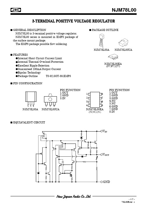
VNO
VIN=9V, Io=40mA VIN=5V ∼ 20V, Io=40mA VIN=6V ∼ 20V, Io=40mA VIN=9V, Io=1 ∼ 40mA VIN=9V, Io=1 ∼ 100mA VIN=9V, Io=0mA VIN=9V, Io=1mA
6V < VIN < 16V, Io=40mA ein=1Vp-p, f=120Hz VIN=9V,BW=10Hz ∼ 100kHz, Io=40mA
9V < VIN < 20V, Io=40mA ein=1Vp-p, f=120Hz VIN=12V,BW=10Hz ∼ 100kHz Io=40mA
NJM78L62A(*2) Output Voltage Line Regulation1
Line Regulation2
Load Regulation1
Vo ∆Vo−VIN1 ∆Vo−VIN2 ∆Vo−Io1 ∆Vo−Io2 IQ ∆Vo/∆T
RR
Output Noise Voltage
VNO
VIN=12V, Io=40mA VIN=8.5V ∼ 20V, Io=40mA VIN=9V ∼ 20V, Io=40mA VIN=12V, Io=1 ∼ 40mA VIN=12V, Io=1 ∼ 100mA VIN=12V, Io=0mA VIN=12V, Io=1mA
Load Regulation2
Quiescent Current
Average Temperature Coefficient of Output Voltage Ripple Rejection
Vo ∆Vo−VIN1 ∆Vo−VIN2 ∆Vo−Io1 ∆Vo−Io2 IQ ∆Vo/∆T
DM78L12中文资料
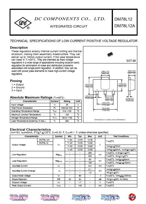
o o o o o o o o
SOT-89
.066(1.70) .059(1.50)
.063(1.60) .055(1.40)
Pinning
1 = Output 2 = Ground 3 = Input
.167(4.25) .159(4.05) 1 2 3 .102(2.60) .095(2.40)
Absolute Maximum Ratings (TA=25oC)
C
C
Electrical Characteristics o o
Characteristic DM78L12A Output Voltage DM78L12
(Vin=19V, Iout=40mA, 0 C TJ 125 C, Cin=0.33mF, Cout=0.1mF, unless otherwise specified)
These regulators empoly internal current limiting and thermal shutdown, making them essentially indestructible. They can deliver up to 100mA output current, if the case temperature o can keep in T C =25 C. They are intended as fixed voltage regulators in a wide range of applications including local(on-card) regulation for elimination of noise and distribution problems associated with single-point regulation. In addition, they can be used with power pass elements to make high-current voltage regulators.
WM8978中文资料
芯片描述 ............................ 14
绪论............................................................... 14 特征............................................................... 14 麦克风输入......................................................... 15 PGA 和 ALC 操作 .....................................................15 线输入(AUXL、AUXR)............................................... 15 ADC................................................................ 15 HI-FI DAC..........................................................15 输出混合器......................................................... 15 音频接口........................................................... 15 控制接口........................................................... 16 时钟配置........................................................... 16 电源控制........................................................... 16 信号输入路线....................................................... 16 麦克风输入......................................................... 16 输入 PGA 音量控制...................................................18 辅助输入........................................................... 19 输入 BOOST .........................................................19 麦克风偏置电路..................................................... 21 模数转换(ADC).................................................... 22 ADC 数字滤波 .......................................................22 可选的高通滤波器................................................... 23 可调陷波滤波器..................................................... 23 数字 ADC 音量控制...................................................24
TS78M18A中文资料

TS78M00A series3-Terminal Medium Current Positive Voltage RegulatorPin assignment:1. Input2. Ground3. Output (Heatsink surfaceconnected to Pin 2)Voltage Range 5V to 24V Output Current up to 0.5AGeneral DescriptionThe TS78M00A Series positive voltage regulators are identical to the popular TS7800 Series devices, except that they are specified for only half the output current. Like the TS7800 devices, the TS78M00A Series 3-Terminal regulators are intended for local, on-card voltage regulation.Internal current limiting, thermal shutdown circuitry and safe-area compensation for the internal pass transistor combine to make these devices remarkably rugged under most operating conditions. Maximum output current with adequate heatsink is 500mAThis series is offered in 3-pin TO-220, TO-252 package.FeaturesOutput current up to 0.5A No external components required Internal thermal overload protection Internal short-circuit current limitingOutput transistor safe-area compensationOutput voltage offered in 2% toleranceOrdering InformationNote: Where xx denotes voltage option. Part No. Operating Temp. (Ambient)PackageTS78MxxACZ TO-220 TS78MxxACP -20 ~ +85o C TO-252 Standard ApplicationA common ground is required between the input and the output voltages. The input voltage must remain typically 2.0V above the output voltage even during the low point on the Input ripple voltage.XX = these two digits of the type number indicate voltage.* = Cin is required if regulator is located an appreciable distance from power supply filter.** = Co is not needed for stability; however, it does improvetransient response.Absolute Maximum RatingInput Voltage Vin * 35 V Input VoltageVin ** 40 V Power Dissipation TO-220 TO-220 TO-252 Without heatsinkPt *** Without heatsink2 15 1 WOperating Junction Temperature Range T J 0 ~ +150 o C Storage Temperature Range T STG-65 ~ +150oCNote : * TS78M05A to TS78M18A ** TS78M24ATS78M05A Electrical Characteristics(Vin=10V, Iout=350mA, 0 o C≤Tj≤125 o C, Cin=0.33uF, Cout=0.1uF; unless otherwise specified.)Parameter Symbol TestConditions MinTypMaxUnitTj=25 o C 4.90 5 5.10Output voltage Vout 7.5V≤Vin≤20V,5mA≤Iout≤350mA, PD≤5W 4.80 5 5.20VLine Regulation REGline Tj=25 o C 7.5V≤Vin≤25V,Io=200mA-- 3 50 5mA≤Iout≤500mA -- 20100Load Regulation REGload Tj=25 o C5mA≤Iout≤200mA -- 10 50mVQuiescent Current Iq Iout=0, Tj=25 o C --367.5V≤Vin≤25V ----0.8 Quiescent Current Change ∆Iq5mA≤Iout≤350mA ----0.5mAOutput Noise Voltage Vn 10Hz≤f≤100KHz, Tj=25 o C -- 40 -- uVRipple Rejection Ratio RR f=120Hz, 8V≤Vin≤18V 62 80 -- dBVoltage Drop Vdrop Iout=350mA, Tj=25 o C --2--V Peak Output Current Io peak Tj=25 o C -- 0.7 -- ATemperature Coefficient of Output Voltage ∆Vout/ ∆Tj Iout=5mA, 0 o C≤Tj≤125 o C -- -0.2 --mV/o CTS78M06A Electrical Characteristics(Vin=11V, Iout=350mA, 0 o C≤Tj≤125 o C, Cin=0.33uF, Cout=0.1uF; unless otherwise specified.)Parameter Symbol TestConditions MinTypMaxUnitTj=25 o C 5.88 6 6.12Output Voltage Vout 8.5V≤Vin≤21V,5mA≤Iout≤350mA, PD≤5W 5.76 6 6.24VLine Regulation REGline Tj=25 o C 8.5V≤Vin≤25V,Io=200mA-- 3 50 5mA≤Iout≤500mA -- 20 120Load Regulation REGload Tj=25 o C5mA≤Iout≤200mA -- 10 60mVQuiescent Current Iq Iout=0, Tj=25 o C --368.5V≤Vin≤25V ----0.8 Quiescent Current Change ∆Iq5mA≤Iout≤350mA ----0.5mAOutput Noise Voltage Vn 10Hz≤f≤100KHz, Tj=25 o C -- 45 -- uVRipple Rejection Ratio RR f=120Hz, 9V≤Vin≤19V 5980--dB Voltage Drop Vdrop Iout=350mA, Tj=25 o C --2--V Output Short Circuit Current Ios Tj=25 o C -- 50 -- mAPeak Output Current Io peak Tj=25 o C -- 0.7 -- ATemperature Coefficient of Output Voltage ∆Vout/ ∆Tj Iout=5mA, 0 o C≤Tj≤125 o C -- -0.2 --mV/o Cz Pulse testing techniques are used to maintain the junction temperature as close to the ambient temperature as possible, and thermal effects must be taken into account separately.z This specification applies only for DC power dissipation permitted by absolute maximum ratings.TS78M08A Electrical Characteristics(Vin=14V, Iout=350mA, 0 o C≤Tj≤125 o C, Cin=0.33uF, Cout=0.1uF; unless otherwise specified.)Parameter Symbol TestConditions MinTypMaxUnitTj=25 o C 7.84 8 8.16Output Voltage Vout 10.5V≤Vin≤23V,5mA≤Iout≤350mA, PD≤5W 7.68 8 8.32VLine Regulation REGline Tj=25 o C 10.5V≤Vin≤25V,Io=200mA-- 6 50 5mA≤Iout≤500mA -- 25 160Load Regulation REGload Tj=25 o C5mA≤Iout≤200mA -- 10 80mVQuiescent Current Iq Iout=0, Tj=25 o C --3610.5V≤Vin≤25V ----0.8 Quiescent Current Change ∆Iq5mA≤Iout≤350mA ----0.5mAOutput Noise Voltage Vn 10Hz≤f≤100KHz, Tj=25 o C -- 52 -- uVRipple Rejection Ratio RR f=120Hz, 11V≤Vin≤21V 5680--dB Voltage Drop Vdrop Iout=350mA, Tj=25 o C --2--V Output Short Circuit Current Ios Tj=25 o C -- 50 -- mAPeak Output Current Io peak Tj=25 o C -- 0.7 -- ATemperature Coefficient of Output Voltage ∆Vout/ ∆Tj Iout=5mA, 0 o C≤Tj≤125 o C -- -0.2 --mV/o CTS78M09A Electrical Characteristics(Vin=15V, Iout=350mA, 0 o C≤Tj≤125 o C, Cin=0.33uF, Cout=0.1uF; unless otherwise specified.)Parameter Symbol TestConditions MinTypMaxUnitTj=25 o COutput Voltage Vout 11.5V≤Vin≤23V,5mA≤Iout≤350mA, PD≤5WLine Regulation REGline Tj=25 o C 11.5V≤Vin≤26V,Io=200mA5mA≤Iout≤500mALoad Regulation REGload Tj=25 o C5mA≤Iout≤200mAQuiescent Current Iq Iout=0, Tj=25 o C11.5V≤Vin≤26VQuiescent Current Change ∆Iq5mA≤Iout≤350mAOutput Noise Voltage Vn 10Hz≤f≤100KHz, Tj=25 o CRipple Rejection Ratio RR f=120Hz, 12V≤Vin≤22VVoltage Drop Vdrop Iout=350mA, Tj=25 o COutput Short Circuit Current Ios Tj=25 o CPeak Output Current Io peak Tj=25 o CTemperature Coefficient ofOutput Voltage∆Vout/ ∆Tj Iout=5mA, 0 o C≤Tj≤125 o Cz Pulse testing techniques are used to maintain the junction temperature as close to the ambient temperature as possible, and thermal effects must be taken into account separately.TS78M10A Electrical Characteristics(Vin=16V, Iout=350mA, 0 o C≤Tj≤125 o C, Cin=0.33uF, Cout=0.1uF; unless otherwise specified.)Parameter Symbol TestConditions MinTypMaxUnitTj=25 o C 9.801010.20Output Voltage Vout 12.5V≤Vin≤25V,5mA≤Iout≤350mA, PD≤5W 9.60 10 10.40VLine Regulation REGline Tj=25 o C 12.5V≤Vin≤28V,Io=200mA-- 8 50 5mA≤Iout≤500mA -- 25 200Load Regulation REGload Tj=25 o C5mA≤Iout≤200mA -- 10 100mVQuiescent Current Iq Iout=0, Tj=25 o C --3612.5V≤Vin≤28V ----0.8 Quiescent Current Change ∆Iq5mA≤Iout≤350mA ----0.5mAOutput Noise Voltage Vn 10Hz≤f≤100KHz, Tj=25 o C -- 70 -- uVRipple Rejection Ratio RR f=120Hz, 13V≤Vin≤23V 5580--dB Voltage Drop Vdrop Iout=350mA, Tj=25 o C --2--V Output Short Circuit Current Ios Tj=25 o C -- 50 -- mAPeak Output Current Io peak Tj=25 o C -- 0.7 -- ATemperature Coefficient of Output Voltage ∆Vout/ ∆Tj Iout=5mA, 0 o C≤Tj≤125 o C -- -0.3 --mV/o CTS78M12A Electrical Characteristics(Vin=19V, Iout=350mA, 0 o C≤Tj≤125 o C, Cin=0.33uF, Cout=0.1uF; unless otherwise specified.)Parameter Symbol TestConditions MinTypMaxUnitTj=25 o C 11.76 12 12.24Output Voltage Vout 14.5V≤Vin≤27V,5mA≤Iout≤350mA, PD ≤5W 11.52 12 12.48VLine Regulation REGline Tj=25 o C 14.5V≤Vin≤30V,Io=200mA-- 8 50 mV 5mA≤Iout≤500mA -- 25 240Load Regulation REGload Tj=25 o C0mA≤Iout≤200mA -- 10 120Quiescent Current Iq Tj=25 o C, Iout=0 -- 3 614.5V≤Vin≤30V ----0.8 Quiescent Current Change ∆Iq5mA≤Iout≤200mA ----0.5mAOutput Noise Voltage Vn 10Hz≤f≤100KHz, Tj=25 o C -- 75 -- uVRipple Rejection Ratio RR f=120Hz, 15V≤Vin≤25V 5580--dB Voltage Drop Vdrop Iout=350mA, Tj=25 o C --2--V Output Short Circuit Current Ios Tj=25 o C -- 50 -- mAPeak Output Current Io peak Tj=25 o C -- 0.7 -- ATemperature Coefficient of Output Voltage ∆Vout/ ∆Tj Iout=5mA, 0 o C≤Tj≤125 o C -- -0.3 --mV/o Cz Pulse testing techniques are used to maintain the junction temperature as close to the ambient temperature as possible, and thermal effects must be taken into account separately.TS78M15A Electrical Characteristics(Vin=23V, Iout=350mA, 0 o C≤Tj≤125 o C, Cin=0.33uF, Cout=0.1uF; unless otherwise specified.)Parameter Symbol TestConditions MinTypMaxUnitTj=25 o C 14.70 15 15.30Output Voltage Vout 17.5V≤Vin≤30V,5mA≤Iout≤350mA, PD ≤5W 14.40 15 15.60VLine Regulation REGline Tj=25o C17.5V≤Vin≤30V,Io=200mA-- 8 50 mV 5mA≤Iout≤500mA -- 25300Load Regulation REGload Tj=25o C 5mA≤Iout≤200mA -- 10150Quiescent Current Iq Tj=25 o C, Iout=0 -- 3 617.5V≤Vin≤30V ----0.8 Quiescent Current Change ∆Iq5mA≤Iout≤350mA ----0.5mAOutput Noise Voltage Vn 10Hz≤f≤100KHz, Tj=25 o C -- 90 -- uVRipple Rejection Ratio RR f=120Hz, 18V≤Vin≤28V 5470--dB Voltage Drop Vdrop Iout=350mA, Tj=25 o C --2--V Output Short Circuit Current Ios Tj=25 o C -- 50 -- mAPeak Output Current Io peak Tj=25 o C -- 0.7 -- ATemperature Coefficient of Output Voltage ∆Vout/ ∆Tj Iout=5mA, 0 o C≤Tj≤125 o C -- -0.3 --mV/o CTS78M18A Electrical Characteristics(Vin=27V, Iout=350mA, 0 o C≤Tj≤125 o C, Cin=0.33uF, Cout=0.1uF; unless otherwise specified.)Parameter Symbol TestConditions MinTypMaxUnitTj=25 o C 17.64 18 18.36Output Voltage Vout 21V≤Vin≤33V,5mA≤Iout≤350mA, PD ≤5W 17.28 18 18.72VLine Regulation REGline Tj=25 o C 21V≤Vin≤33V,Io=200mA-- 8 50 mV 5mA≤Iout≤500mA -- 25 360Load Regulation REGload Tj=25 o C5mA≤Iout≤200mA -- 10 180Quiescent Current Iq Tj=25 o C, Iout=0 -- 3 621V≤Vin≤33V ----0.8 Quiescent Current Change ∆Iq5mA≤Iout≤350nA ----0.5mAOutput Noise Voltage Vn 10Hz≤f≤100KHz, Tj=25 o C --110--uV Ripple Rejection Ratio RR f=120Hz, 21V≤Vin≤31V 5470--dB Voltage Drop Vdrop Iout=350mA, Tj=25 o C --2--V Output Short Circuit Current Ios Tj=25 o C -- 50 -- mAPeak Output Current Io peak Tj=25 o C -- 0.7 -- ATemperature Coefficient of Output Voltage ∆Vout/ ∆Tj Iout=5mA, 0 o C≤Tj≤125 o C -- -0.5 --mV/o Cz Pulse testing techniques are used to maintain the junction temperature as close to the ambient temperature as possible, and thermal effects must be taken into account separately.TS78M24A Electrical Characteristics(Vin=33V, Iout=350mA, 0 o C≤Tj≤125 o C, Cin=0.33uF, Cout=0.1uF; unless otherwise specified.)Parameter Symbol TestConditions MinTypMaxUnitTj=25 o C 23.52 24 24.48Output Voltage Vout 27V≤Vin≤38V,5mA≤Iout≤350mA, PD ≤5W 22.04 24 25.96VLine Regulation REGline Tj=25 o C 27V≤Vin≤38V,Io=200mA-- 10 50 mV 5mA≤Iout≤500mA -- 30 480Load Regulation REGload Tj=25 o C5mA≤Iout≤200mA -- 10 240Quiescent Current Iq Iout=0, Tj=25 o C --4727V≤Vin≤38V ----0.8 Quiescent Current Change ∆Iq5mA≤Iout≤350mA ----0.5mAOutput Noise Voltage Vn 10Hz≤f≤100KHz, Tj=25 o C --170--uV Ripple Rejection Ratio RR f=120Hz, 27V≤Vin≤37V 5070--dB Voltage Drop Vdrop Iout=350mA, Tj=25 o C --2--V Output Short Circuit Current Ios Tj=25 o C -- 50 -- mAPeak Output Current Io peak Tj=25 o C -- 0.7 -- ATemperature Coefficient of Output Voltage ∆Vout/ ∆Tj Iout=5mA, 0 o C≤Tj≤125 o C -- -0.5 --mV/o Cz Pulse testing techniques are used to maintain the junction temperature as close to the ambient temperature as possible, and thermal effects must be taken into account separately.z This specification applies only for DC power dissipation permitted by absolute maximum ratings.Electrical Characteristics CurveFIGURE 1 - Worst Case Power Dissipation v.s.Ambient TemperatureFIGURE 2 - Peak Output Current v.s.Dropout VoltageFIGURE 3 – Quiescent Current v.s.Input VoltageFIGURE 4 –Dropout Voltage v.s.Junction TemperatureFIGURE 5 – Quiescent Current v.s.Output CurrentFIGURE 6 – TO-252 Thermal Resistance andPd(max) v.s. P.C.B Copper LengthElectrical Characteristics CurveFIGURE 7 – Ripple Rejection v.s.FrequencyFIGURE 8 – Ripple Rejection v.s.Output Voltage。
KA78L15AZ资料
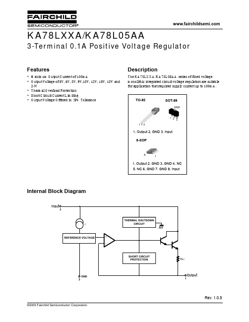
©2005 Fairchild Semiconductor CorporationRev. 1.0.5Features•Maximum Output Current of 100mA•Output V oltage of 5V , 6V , 8V , 9V ,10V , 12V , 15V , 18V and 24V•Thermal Overload Protection •Short Circuit Current Limiting•Output V oltage Offered in ±5% ToleranceDescriptionThe KA78LXXA/KA78L05AA series of fixed voltage monolithic integrated circuit voltage regulators are suitable for application that required supply current up to 100mA.TO-921. Output2. GND3. Input 8-SOP1. Output2. GND3. GND4. NC5. NC6. GND7. GND8. Input11SOT-891GND23238KA78LXXA/KA78L05AA3-Terminal 0.1A Positive Voltage RegulatorKA78LXXA/KA78L05AA2Absolute Maximum RatingsElectrical Characteristics(KA78L05A)(V I = 10V, I O = 40mA, 0°C ≤ T J ≤ 125°C, C I = 0.33µF, C O = 0.1µF, unless otherwise specified. (Note1)Note:1.The maximum steady state usable output current and input voltage are very dependent on the heat sinking and/or lead lengthof the package. The data above represent pulse test conditions with junction temperature as indicated at the initiation of tests.2.Power dissipation P D ≤ 0.75W.ParameterSymbol Value Unit Input Voltage (for V O = 5V, 8V)(for V O = 12V to 18V)(for V O = 24VV I 303540V V V Operating Junction Temperature Range T J 0 ~ +150°C Storage Temperature RangeT STG-65 ~ +150°CParameter Symbol ConditionsMin.Typ.Max.Unit Output Voltage V O T J = 25°C 4.8 5.0 5.2V Line Regulation (Note1)∆V O T J = 25°C 7V ≤ V I ≤ 20V -8150mV 8V ≤ V I ≤ 20V -6100mV Load Regulation (Note1)∆V OT J = 25°C 1mA ≤ I O ≤ 100mA -1160mV 1mA ≤ I O ≤ 40mA - 5.030mV Output Voltage V O 7V ≤ V I ≤ 20V1mA ≤ I O ≤ 40mA -- 5.25V 7V ≤V I ≤ V MAX (Note2)1mA ≤ I O ≤ 70mA 4.75- 5.25V Quiescent Current I Q T J = 25°C - 2.0 5.5mA Quiescent Current ChangeWith Line ∆I Q 8V ≤V I ≤ 20V -- 1.5mA With Load∆I Q 1mA ≤ I O ≤ 40 mA--0.1mA Output Noise Voltage V N T A = 25°C, 10Hz ≤ f ≤ 100kHz -40-µV/Vo Temperature Coefficient of V O ∆V O /∆T I O = 5mA--0.65-mV/°C Ripple Rejection RR f = 120Hz, 8V ≤ V I ≤ 18V, T J = 25°C 4180-dB Dropout VoltageV DT J = 25°C- 1.7-VKA78LXXA/KA78L05AA3Electrical Characteristics(KA78L06A) (Continued)(V I = 12V, I O = 40mA, 0°C ≤ T J ≤ 125°C, C I = 0.33µF, C O = 0.1µF, unless otherwise specified. (Note 1)Note:1.The maximum steady state usable output current and input voltage are very dependent on the heat sinking and/or lead lengthof the package. The data above represent pulse test conditions with junction temperature as indicated at the initiation of tests.2.Power dissipation P D ≤ 0.75W.Parameter Symbol ConditionsMin.Typ.Max.Unit Output Voltage V O T J = 25°C 5.75 6.0 6.25V Line Regulation (Note1)∆V O T J = 25°C 8.5V ≤ V I ≤ 20V -64175mV 9V ≤ V I ≤ 20V -54125mV Load Regulation (Note1)∆V O T J = 25°C1mA ≤ I O ≤ 100mA -12.880mV 1mA ≤ I O ≤ 70mA - 5.840mV Output Voltage V O 8.5 ≤ V I ≤ 20V, 1mA ≤ I O ≤ 40mA 5.7- 6.3V 8.5 ≤ V I ≤ V MAX (Note), 1mA ≤ I O ≤ 70mA 5.7- 6.3V Quiescent Current I QT J = 25°C -- 5.5mA T J = 125°C - 3.9 6.0mA Quiescent Current ChangeWith Line ∆I Q 9 ≤ V I ≤ 20V -- 1.5mA With Load∆I Q 1mA ≤ I O ≤ 40mA--0.1mA Output Noise Voltage V N T A = 25°C, 10Hz ≤ f ≤ 100kHz -40-µV/Vo Temperature Coefficient of V O ∆V O /∆T I O = 5mA-0.75-mV/°C Ripple Rejection RR f = 120Hz, 10V ≤ V I ≤ 20V, T J = 25°C 4046-dB Dropout VoltageV DT J = 25°C- 1.7-VKA78LXXA/KA78L05AA4Electrical Characteristics(KA78L08A) (Continued)(V I = 14V, I O = 40mA, 0°C ≤ T J ≤ 125°C, C I = 0.33µF, C O = 0.1µF, unless otherwise specified. (Note1)Note:1.The maximum steady state usable output current and input voltage are very dependent on the heat sinking and/or lead lengthof the package. The data above represent pulse test conditions with junction temperature as indicated at the initiation of tests.2.Power dissipation P D ≤ 0.75W.Parameter Symbol ConditionsMin.Typ.Max.Unit Output Voltage V O T J = 25°C 7.78.08.3V Line Regulation (Note1)∆V O T J = 25°C 10.5V ≤ V I ≤ 23V -10175mV 11V ≤ V I ≤ 23V -8125mV Load Regulation (Note1)∆V OT J = 25°C1mA ≤ I O ≤ 100mA -1580mV 1mA ≤ I O ≤ 40mA -8.040mV Output Voltage V O 10.5V ≤ V I ≤ 23V 1mA ≤ I O ≤ 40mA7.6-8.4V 10.5V ≤ V I ≤ V MAX (Note2)1mA ≤ I O ≤ 70mA7.6-8.4V Quiescent Current I Q T J = 25°C - 2.0 5.5mA Quiescent Current ChangeWith Line ∆I Q 11V ≤ V I ≤ 23V -- 1.5mA With Load∆I Q 1mA ≤ I O ≤ 40mA--0.1mA Output Noise Voltage V N T A = 25°C, 10Hz ≤ f ≤100kHz -60-µV/Vo Temperature Coefficient of V O ∆V O /∆T I O = 5mA--0.8-mV/°C Ripple Rejection RR f = 120Hz, 11V ≤ V I ≤ 21V, T J = 25°C 3970-dB Dropout VoltageV DT J = 25°C- 1.7-VKA78LXXA/KA78L05AA5Electrical Characteristics(KA78L09A) (Continued)(V I = 15V, I O = 40mA, 0°C ≤ T J ≤ 125°C, C I = 0.33µF, C O = 0.1µF, unless otherwise specified. (Note1)Note:1.The maximum steady state usable output current and input voltage are very dependent on the heat sinking and/or lead lengthof the package. The data above represent pulse test conditions with junction temperature as indicated at the initiation of tests.2.Power dissipation P D ≤ 0.75W.Parameter Symbol ConditionsMin.Typ.Max.Unit Output Voltage V O T J = 25°C 8.649.09.36V Line Regulation (Note1)∆V O T J = 25°C 11.5V ≤ V I ≤ 24V -90200mV 13V ≤ V I ≤ 24V -100150mV Load Regulation (Note1)∆V OT J = 25°C1mA ≤ I O ≤ 100mA -2090mV 1mA ≤ I O ≤ 40mA -1045mV Output Voltage V O 11.5V ≤ V I ≤ 24V 1mA ≤ I O ≤ 40mA8.55-9.45V 11.5V ≤ V I ≤ V MAX (Note 2)1mA ≤ I O ≤ 70mA8.55-9.45V Quiescent Current I Q T J = 25°C - 2.1 6.0mA Quiescent Current ChangeWith Line ∆I Q 13V ≤ V I ≤ 24V -- 1.5mA With Load∆I Q 1mA ≤ I O ≤ 40mA--0.1mA Output Noise Voltage V N T A = 25°C, 10Hz ≤ f ≤ 100kHz -70-µV/Vo Temperature Coefficient of V O ∆V O /∆T I O = 5mA--0.9-mV/°C Ripple Rejection RR f = 120Hz, 12V ≤ V I ≤ 22V, T J = 25°C 3844-dB Dropout VoltageV DT J = 25°C- 1.7-VKA78LXXA/KA78L05AA6Electrical Characteristics(KA78L10A) (Continued)(V I = 16V, I O = 40mA, 0 °C ≤ T J ≤ 125 °C, C I = 0.33 µF, C O = 0.1µF, unless otherwise specified. (Note1)Notes:1.The maximum steady state usable output current and input voltage are very dependent on the heat sinking and/or lead lengthof the package. The data above represent pulse test conditions with junction temperature as indicated at the initiation of tests.2.Power dissipation P D ≤ 0.75W.Parameter Symbol ConditionsMin.Typ.Max.Unit Output Voltage V O T J = 25°C 9.610.010.4V Line Regulation (Note1)∆V O T J = 25°C 12.5 ≤ V I ≤ 25V -100220mV 14V ≤ V I ≤ 25V -100170mV Load Regulation (Note1)∆V OT J = 25°C1mA ≤ I O ≤ 100mA -2094mV 1mA ≤ I O ≤ 70mA -1047mVOutput VoltageV O12.5V ≤ V I ≤ 25V, 1mA ≤ I O ≤ 40mA9.5-10.5V 12.5V ≤ V I ≤ V MAX (Note2)1mA ≤ I O ≤ 70mA 9.5-10.5Quiescent Current I Q T J = 25°C -- 6.0mA T J =125°C - 4.2 6.5Quiescent Current ChangeWith Line ∆I Q 12.5 ≤ V I ≤ 25V -- 1.5mA With Load∆I Q 1mA ≤ I O ≤ 40mA--0.1mA Output Noise Voltage V N T A = 25°C, 10Hz ≤ f ≤ 100kHz -74-µV/Vo Temperature Coefficient of V O ∆V O /∆T I O = 5mA-0.95-mV/°C Ripple Rejection RR f = 120Hz, 15V ≤ V I ≤ 25V, T J = 25°C 3843-dB Dropout VoltageV DT J = 25°C-1.7-VKA78LXXA/KA78L05AA7Electrical Characteristics(KA78L12A) (Continued)(V I = 19V, I O = 40mA, 0°C ≤ T J ≤ 125°C, C I = 0.33 µF, C O = 0.1µF, unless otherwise specified. (Note 1)Note:1.The maximum steady state usable output current and input voltage are very dependent on the heat sinking and/or lead lengthof the package. The data above represent pulse test conditions with junction temperature as indicated at the initiation of tests.2.Power dissipation P D ≤ 0.75W.Parameter Symbol ConditionsMin.Typ.Max.Unit Output Voltage V O T J = 25°C 11.51212.5V Line Regulation (Note1)∆V O T J = 25°C 14.5V ≤ V I ≤ 27V -20250mV 16V ≤ V I ≤ 27V -15200mV Load Regulation (Note1)∆V OT J = 25°C1mA ≤ I O ≤ 100mA -20100mV 1mA ≤ I O ≤ 40mA-1050mV Output Voltage V O 14.5V ≤ V I ≤ 27V 1mA ≤ I O ≤ 40mA11.4-12.6V 14.5V ≤ V I ≤ V MAX (Note 2)1mA ≤ I O ≤ 70mA 11.4-12.6V Quiescent Current I Q T J = 25°C - 2.1 6.0mA Quiescent Current ChangeWith Line ∆I Q 16V ≤ V I ≤ 27V -- 1.5mA With Load∆I Q 1mA ≤ I O ≤ 40mA--0.1mA Output Noise Voltage V N T A = 25°C, 10Hz ≤ f ≤ 100kHz -80-µV/Vo Temperature Coefficient of V O ∆V O /∆T I O = 5mA--1.0-mV/°C Ripple Rejection RR f = 120Hz, 15V ≤ V I ≤ 25V, T J = 25°C 3765-dB Dropout VoltageV DT J = 25°C- 1.7-VKA78LXXA/KA78L05AA8Electrical Characteristics(KA78L15A) (Continued)(V I = 23V, I O = 40mA, 0°C ≤ T J ≤ 125°C, C I = 0.33 µF, C O = 0.1µF, unless otherwise specified. (Note1)Note:1.The maximum steady state usable output current and input voltage are very dependent on the heat sinking and/or lead lengthof the package. The data above represent pulse test conditions with junction temperature as indicated at the initiation of tests.2.Power dissipation P D ≤ 0.75W.Parameter Symbol ConditionsMin.Typ.Max.Unit Output Voltage V O T J = 25°C 14.41515.6V Line Regulation (Note1)∆V O T J = 25°C 17.5V ≤ V I ≤ 30V -25300mV 20V ≤ V I ≤ 30V -20250mV Load Regulation (Note1)∆V OT J = 25°C 1mA ≤ I O ≤ 100mA -25150mV 1mA ≤ I O ≤ 40mA -1275mV Output VoltageV O 17.5V ≤ V I ≤ 30V1mA ≤ I O ≤ 40mA 14.25-15.75V 17.5V ≤ V I ≤ V MAX (Note 2)1mA ≤ I O ≤ 70mA 14.25-15.75V Quiescent Current I QT J = 25°C - 2.1 6.0mA Quiescent Current ChangeWith Line ∆I Q 20V ≤ V I ≤ 30V -- 1.5mA With Load∆I Q 1mA ≤ I O ≤ 40mA--0.1mA Output Noise Voltage V N T A = 25°C, 10Hz ≤ f ≤ 100kHz -90-µV/Vo Temperature Coefficient of V O ∆V O /∆T I O = 5mA--1.3-mV/°C Ripple Rejection RR f = 120Hz, 18.5V ≤ V I ≤ 28.5V, T J = 25°C 3460-dB Dropout VoltageV DT J = 25°C- 1.7-VKA78LXXA/KA78L05AA9Electrical Characteristics(KA78L18A) (Continued)(V I = 27V, I O = 40mA, 0°C ≤ T J ≤ 125°C, C I = 0.33 µF, C O = 0.1µF, unless otherwise specified. (Note1)Note:1.The maximum steady state usable output current and input voltage are very dependent on the heat sinking and/or lead lengthof the package. The data above represent pulse test conditions with junction temperature as indicated at the initiation of tests.2.Power dissipation P D ≤ 0.75W.Parameter Symbol ConditionsMin.Typ.Max.Unit Output Voltage V O T J = 25°C 17.31818.7V Line Regulation (Note1)∆V O T J = 25°C 21V ≤ V I ≤ 33V -145300mV 22V ≤ V I ≤ 33V -135250mV Load Regulation (Note1)∆V OT J = 25°C 1mA ≤ I O ≤100mA -30170mV 1mA ≤ I O ≤ 40mA -1585mV Output Voltage V O 21V ≤ V I ≤ 33V1mA ≤ I O ≤ 40mA 17.1-18.9V 21V ≤ V I ≤ V MAX (Note 2)1mA ≤ I O ≤ 70mA 17.1-18.9V Quiescent Current I Q T J = 25°C - 2.2 6.0mA Quiescent Current ChangeWith Line ∆I Q 21V ≤ V I ≤ 33V -- 1.5mA With Load∆I Q 1mA ≤ I O ≤ 40mA--0.1mA Output Noise Voltage V N T A = 25°C, 10Hz ≤ f ≤ 100kHz -150-µV/Vo Temperature Coefficient of V O ∆V O /∆T I O = 5mA--1.8-mV/°C Ripple Rejection RR f = 120Hz, 23V ≤ V I ≤ 33V, T J = 25°C 3448-dB Dropout VoltageV DT J = 25°C- 1.7-VKA78LXXA/KA78L05AA10Electrical Characteristics(KA78L24A) (Continued)(V I = 33V, I O = 40mA, 0°C ≤ T J ≤ 125°C, C I = 0.33 µF, C O = 0.1µF, unless otherwise specified. (Note1)Note:1.The maximum steady state usable output current and input voltage are very dependent on the heat sinking and/or lead lengthof the package. The data above represent pulse test conditions with junction temperature as indicated at the initiation of tests.2.Power dissipation P D ≤ 0.75W.Parameter Symbol ConditionsMin.Typ.Max.Unit Output Voltage V O T J = 25°C 232425V Line Regulation (Note1)∆V O T J = 25°C 27V ≤ V I ≤ 38V -160300mV 28V ≤ V I ≤ 38V -150250mV Load Regulation (Note1)∆V OT J = 25°C 1mA ≤ I O ≤ 100mA -40200mV 1mA ≤ I O ≤ 40mA -20100mV Output Voltage V O 27V ≤ V I ≤ 38V1mA ≤ I O ≤ 40mA 22.8-25.2V 27V ≤ V I ≤ V MAX (Note2)1mA ≤ I O ≤ 70mA 22.8-25.2V Quiescent Current I Q T J = 25°C - 2.2 6.0mA Quiescent Current ChangeWith Line ∆I Q 28V ≤ V I ≤ 38V -- 1.5mA With Load∆I Q 1mA ≤ I O ≤ 40mA--0.1mA Output Noise Voltage V N T A = 25°C, 10Hz ≤ f ≤ 100kHz -200-µV/Vo Temperature Coefficient of V O ∆V O /∆T I O = 5mA--2.0-mV/°C Ripple Rejection RR f = 120Hz, 28V ≤ V I ≤ 38V, T J = 25°C 3445-dB Dropout VoltageV DT J = 25°C- 1.7-V11Absolute Maximum RatingsElectrical Characteristics(KA78L05AA) (Continued)(V I = 10V, I O = 40mA, 0°C ≤ T J ≤ 125°C, C I = 0.33 µF, C O = 0.1µF, unless otherwise specified. (Note1)Note:1. The maximum steady state usable output current and input voltage are very dependent on the heat sinking and/or lead lengthof the package. The data above represent pulse test conditions with junction temperature as indicated at the initiation of tests.2. Power dissipation P D ≤ 0.75W.ParameterSymbol Value Unit Input Voltage (for V O = 5V, 8V)(for V O = 12V to 18V)(for V O = 24VV I 303540V V V Operating Junction Temperature Range T J 0 ~ +150°C Storage Temperature RangeT STG-65 ~ +150°CParameter Symbol ConditionsMin.Typ.Max.Unit Output Voltage V O T J = 25°C 4.9 5.0 5.1V Line Regulation (Note1)∆V O T J = 25°C 7V ≤ V I ≤ 20V -8150mV 8V ≤ V I ≤ 20V -6100mV Load Regulation (Note1)∆V OT J = 25°C 1mA ≤ I O ≤ 100mA -1150mV 1mA ≤ I O ≤ 40mA - 5.025mV Output Voltage V O 7V ≤V I ≤ 20V1mA ≤ I O ≤ 40mA -- 5.15V 7V ≤V I ≤ V MAX (Note2)1mA ≤ I O ≤ 70mA 4.85- 5.15V Quiescent Current I Q T J = 25°C - 2.0 5.5mA Quiescent Current ChangeWith Line ∆I Q 8V ≤V I ≤ 20V -- 1.5mA With Load∆I Q 1mA ≤ I O ≤ 40 mA--0.1mA Output Noise Voltage V N T A = 25°C, 10Hz ≤ f ≤ 100kHz -40-µV/Vo Temperature Coefficient of V O ∆V O /∆T I O = 5mA--0.65-mV/°C Ripple Rejection RR f = 120Hz, 8V ≤ V I ≤ 18V, T J = 25°C 4180-dB Dropout VoltageV DT J = 25°C- 1.7-VTypical Application’( )’ : 8SOP TypeNote:1.To specify an output voltage, substitute voltage value for “XX”.2.Bypass Capacitors are recommend for optimum stability and transient response and should be located as close as possibleto the regulator12Mechanical DimensionsPackageDimensions in millimetersTO-9213PackageDimensions in millimeters8-SOPSymbol Min Nom MaxA-- 1.75A10.100.150.25A2 1.25 1.45 1.50B0.350.370.51C0.190.200.25D 4.80 4.90 5.00E 3.80 3.90 4.00e 1.27BSCH 5.79 5.99 6.20h0.25-0.50L0.500.700.90GP0.36 BSCq0-8aaa--0.25bbb--0.1014PackageDimensions in millimetersSOT-891516Ordering InformationNote:1. For information on tape & reel and ammo pack specifications, including part orientation and tape sizes, please refer to our tapeand reel data, /products/analog/pdf/to92r_tr.pdf.Product Number PackagePacking Output Voltage Tolerance Operating TemperatureKA78L05AZTA TO-92Ammo 5%0 ~ +125 °CKA78L05AZTF Tape & ReelKA78L05AZBU Bulk KA78L06AZTA Ammo KA78L06AZBU Tape & Reel KA78L08AZTA Ammo KA78L08AZTF Tape & ReelKA78L08AZBU Bulk KA78L09AZTA Ammo KA78L09AZBU Tape & Reel KA78L10AZTA Ammo KA78L10AZBU Tape & Reel KA78L12AZTA Ammo KA78L12AZTF Tape & ReelKA78L12AZBU Bulk KA78L15AZTA Ammo KA78L15AZBU Tape & Reel KA78L18AZTA Ammo KA78L18AZBU Tape & Reel KA78L24AZTA Ammo KA78L05AMTF SOT-89Tape & Reel KA78L05AMTM Tape & Reel KA78L08AMTF Tape & Reel KA78L09AMTF Tape & Reel KA78L12AMTF Tape & ReelKA78L05AD 8-SOP Tube KA78L05ADTF Tape & ReelKA78L08AD Tube KA78L08ADTF Tape & ReelKA78L12AD Tube KA78L12ADTF Tape & Reel KA78L05AAZTA TO-92Ammo 2%KA78L05AAZBUBulk175/17/05 0.0m 001Stock#DSxxxxxxxx2005 Fairchild Semiconductor CorporationLIFE SUPPORT POLICYFAIRCHILD’S PRODUCTS ARE NOT AUTHORIZED FOR USE AS CRITICAL COMPONENTS IN LIFE SUPPORT DEVICES OR SYSTEMS WITHOUT THE EXPRESS WRITTEN APPROVAL OF THE PRESIDENT OF FAIRCHILD SEMICONDUCTOR CORPORATION. As used herein:1.Life support devices or systems are devices or systemswhich, (a) are intended for surgical implant into the body, or (b) support or sustain life, and (c) whose failure to perform when properly used in accordance with instructions for use provided in the labeling, can bereasonably expected to result in a significant injury of the user.2. A critical component in any component of a life supportdevice or system whose failure to perform can bereasonably expected to cause the failure of the life support device or system, or to affect its safety or effectiveness.DISCLAIMERFAIRCHILD SEMICONDUCTOR RESERVES THE RIGHT TO MAKE CHANGES WITHOUT FURTHER NOTICE TO ANY PRODUCTS HEREIN TO IMPROVE RELIABILITY, FUNCTION OR DESIGN. FAIRCHILD DOES NOT ASSUME ANYLIABILITY ARISING OUT OF THE APPLICATION OR USE OF ANY PRODUCT OR CIRCUIT DESCRIBED HEREIN; NEITHER DOES IT CONVEY ANY LICENSE UNDER ITS PATENT RIGHTS, NOR THE RIGHTS OF OTHERS.。
- 1、下载文档前请自行甄别文档内容的完整性,平台不提供额外的编辑、内容补充、找答案等附加服务。
- 2、"仅部分预览"的文档,不可在线预览部分如存在完整性等问题,可反馈申请退款(可完整预览的文档不适用该条件!)。
- 3、如文档侵犯您的权益,请联系客服反馈,我们会尽快为您处理(人工客服工作时间:9:00-18:30)。
DescriptionsThis series of fixed-voltage monolithic integrated-circuit voltage regulators is designed for awide range of applications. These applications include on-card regulation for elimination ofNoise and distribution problems associated with single-point regulation. In addition, they can be used with power-pass elements to make high-current voltage regulators. Each ofThese regulators can deliver up to 100mA of output current. The internal limiting andthermal shutdown features of these regulators make them essentially immune to overload.When used as a replacement for a Zener diode-resistor combination, on effectiveimprovement in output impedance can be obtained together with lover-bias current. Features• 3-Terminal Regulators• Output Current Up to 100mA• No External Components• Internal Thermal Overload Protection• Internal Short-Circuit LimitingOrdering InformationType NO. Marking Package CodeS78Lxx S78Lxx TO-92Outline Dimensions unit : mmAbsolute maximum ratings(Ta=25°C) Characteristics Symbol Ratings UnitS78L05ThruS78L1030S78L12 Thru S78L18 35Operating Input Voltage V INS78L24 40VPower Dissipation P D 625 ㎽Operating Temperature Range T OPR-40 ~ +85 ℃Junction Temperature T J 150 ℃Storage Temperature Range T STG-55 ~ +150 ℃Lead Temperature Time T SOL 260(10sec) ℃Recommended operating conditionsParameter Min.Max.UnitS78L05 7 20S78L06 8 20S78L08 10.5 23S78L09 11.5 24S78L10 12.5 25S78L12 14.5 27S78L15 17.5 30S78L18 20.5 33Input Voltage, V IS78L24 26.5 39VOutput current, I O100mA(V I =10V, I O =40㎃, T J =0 ~ ℃125, Unless otherwise noted)℃S78L06 Electrical Characteristics(V I =11V, I O =40㎃, T J =0 ~℃ 1 25, Unless otherwise noted)℃S78L06Parameter Test Conditions*Min. Typ. Max.Unit25℃ 5.75 6 6.25I O =1mA to 40mA V I =8V to 20V 5.7 6 6.3 Output Voltage **I O =1mA to 70mA0℃ to 125℃5.7 66.3 VV I =8V to 20V35175Input regulation V I =9V to 20V 25℃ 29 125 mVRipple rejection V I =9V to 19V, f=120Hz 0℃ to 25℃40 48 dB I O =1mA to 100mA1680Output regulation I O =1mA to 40mA 25℃ 9 40 mV Output noise voltage f=10Hz to 100KHz25℃ 46 uV Dropout Voltage 25℃ 1.7 V 25℃ 3.9 6 Bias current125℃ 5.5V I =9V to 20V 1.5 Bias Current ChangeI O =1mA to 40mA0℃ to 125℃0.1 mA* Pulse testing techniques are used to maintain the junction temperature as close to the ambient temperature as possible. Thermal effects must be taken into account separately. All characteristics are measured with a 0.33uF capacitor across the input and a 0.1uF capacitor across the output.** This specification applies only for dc power dissipation permitted by absolute maximum ratings.S78L05Parameter Test Conditions*Min. Typ. Max.Unit25℃ 4.8 5 5.2 I O =1mA to 40mA V I =7V to 20V 4.75 5 5.25 Output Voltage **I O =1mA to 70mA 0℃ to 125℃4.75 55.25VV I =7V to 20V32150Input regulation V I =8V to 20V 25℃ 26 100 mVRipple rejection V I =8V to 18V, f=120Hz 0℃ to 25℃41 49 dB I O =1mA to 100mA1560Output regulation I O =1mA to 40mA 25℃ 8 30 mV Output noise voltage f=10Hz to 100KHz25℃ 42 uV Dropout Voltage 25℃ 1.7 V 25℃ 3.8 6 Bias current125℃ 5.5V I =8V to 20V 1.5 Bias Current ChangeI O =1mA to 40mA0℃ to 125℃0.1 mA(V I =14V, I O =40㎃, T J =0 ~ ℃125, Unless otherwise noted)℃S78L08Parameter Test Conditions*Min. Typ. Max.Unit25℃ 7.7 8 8.3 I O =1mA to 40mA V I =10.5V to 23V 7.6 8 8.4 Output Voltage **I O =1mA to 70mA 0℃ to 125℃7.6 8 8.4VV I =10.5V to 23V42175Input regulation V I =11V to 23V 25℃ 36 125 mVRipple rejection V I =13V to 23V, f=120Hz0℃ to 25℃37 46 dB I O =1mA to 100mA1880Output regulation I O =1mA to 40mA 25℃ 10 40 mV Output noise voltage f=10Hz to 100KHz25℃ 54 uV Dropout Voltage 25℃ 1.7 V 25℃ 4 6 Bias current125℃ 5.5V I =11V to 23V 1.5 Bias Current ChangeI O =1mA to 40mA0℃ to 125℃0.1mAS78L09 Electrical Characteristics(V I =16V, I O =40㎃, T J =0 ~ ℃125, Unless otherwise noted)℃S78L09Parameter Test Conditions*Min. Typ. Max.Unit25℃ 8.6 9 9.4I O =1mA to 40mA V I =12V to 24V 8.55 9 9.45 Output Voltage **I O =1mA to 70mA0℃ to 125℃8.55 9 9.45 VV I =12V to 24V45175Input regulation V I =13V to 24V 25℃ 40 125 mVRipple rejection V I =15V to 25V, f=120Hz0℃ to 25℃38 45 dB I O =1mA to 100mA1990Output regulation I O =1mA to 40mA 25℃ 11 40 mV Output noise voltage f=10Hz to 100KHz25℃ 58 uV Dropout Voltage 25℃ 1.7 V 25℃ 4.1 6 Bias current125℃ 5.5V I =13V to 24V 1.5 Bias Current ChangeI O =1mA to 40mA0℃ to 125℃0.1 mA* Pulse testing techniques are used to maintain the junction temperature as close to the ambient temperature as possible. Thermal effects must be taken into account separately. All characteristics are measured with a 0.33uF capacitor across the input and a 0.1uF capacitor across the output.** This specification applies only for dc power dissipation permitted by absolute maximum ratings.(V I =17V, I O =40㎃, T J =0 ~ ℃125, Unless ℃ otherwise noted)S78L10Parameter Test Conditions*Min. Typ. Max.Unit25℃ 9.6 10 10.4 I O =1mA to 40mA V I =13V to 25V 9.5 10 10.5 Output Voltage **I O =1mA to 70mA 0℃ to 125℃9.5 10 10.5VV I =13V to 25V51175Input regulation V I =14V to 25V 25℃ 42 125 mVRipple rejection V I =15V to 25V, f=120Hz0℃ to 25℃37 44 dB I O =1mA to 100mA2090Output regulation I O =1mA to 40mA 25℃ 11 40 mV Output noise voltage f=10Hz to 100KHz25℃ 62 uV Dropout Voltage 25℃ 1.7 V 25℃ 4.2 6 Bias current125℃ 5.5V I =14V to 25V 1.5 Bias Current ChangeI O =1mA to 40mA0℃ to 125℃0.1 mAS78L12 Electrical Characteristics(V I =19V, I O =40㎃, T J =0 ~ ℃125, Unless otherwise noted)℃S78L12Parameter Test Conditions*Min. Typ. Max.Unit25℃ 11.5 12 12.5I O =1mA to 40mA V I =14V to 27V 11.4 12 12.6 Output Voltage **I O =1mA to 70mA0℃ to 125℃11.4 12 12.6 VV I =14.5V to 27V55250Input regulation V I =16V to 27V 25℃ 49 200 mVRipple rejection V I =15V to 25V, f=120Hz0℃ to 25℃37 42 dB I O =1mA to 100mA22100Output regulation I O =1mA to 40mA 25℃ 13 50 mV Output noise voltage f=10Hz to 100KHz25℃ 70 uV Dropout Voltage 25℃ 1.7 V 25℃ 4.3 6.5 Bias current125℃ 6V I =16V to 27V 1.5 Bias Current ChangeI O =1mA to 40mA0℃ to 125℃0.1mA* Pulse testing techniques are used to maintain the junction temperature as close to the ambient temperature as possible. Thermal effects must be taken into account separately. All characteristics are measured with a 0.33uF capacitor across the input and a 0.1uF capacitor across the output.** This specification applies only for dc power dissipation permitted by absolute maximum ratings.(V I =23V, I O =40㎃, T J =0 ~ ℃125, Unless otherwise n ℃oted)S78L15Parameter Test Conditions*Min. Typ. Max.Unit25℃ 14.4 15 15.6 I O =1mA to 40mA V I =17.5V to 30V 14.25 15 15.75 Output Voltage **I O =1mA to 70mA 0℃ to 125℃14.25 15 15.75VV I =17.5V to 30V65300Input regulation V I =19V to 30V25℃ 58 250 mVRipple rejection V I =18.5V to 28.5V, f=120Hz0℃ to 25℃34 39 dB I O =1mA to 100mA25150Output regulation I O =1mA to 40mA 25℃ 15 75 mV Output noise voltage f=10Hz to 100KHz25℃ 82 uV Dropout Voltage 25℃ 1.7 V 25℃ 4.6 6.5 Bias current125℃ 6V I =19V to 30V 1.5 Bias Current ChangeI O =1mA to 40mA0℃ to 125℃0.1mAS78L18 Electrical Characteristics(V I =26V, I O =40㎃, T J =0 ~ ℃125, Unless otherwise noted)℃S78L18Parameter Test Conditions* Min. Typ. Max.Unit25℃ 17.3 18 18.7 I O =1mA to 40mA V I =20.5V to 33V 17.1 18 18.9 Output Voltage **I O =1mA to 70mA0℃ to 125℃17.1 18 18.9 VV I =20.5V to 33V70360Input regulation V I =22V to 33V25℃ 64 300 mVRipple rejection V I =21.5V to 31.5V,f=120Hz0℃ to 25℃32 36 dB I O =1mA to 100mA27180Output regulation I O =1mA to 40mA 25℃ 19 90 mV Output noise voltage f=10Hz to 100KHz25℃ 89 uV Dropout Voltage 25℃ 1.7 V 25℃ 4.7 6.5 Bias current125℃ 6V I =22V to 33V 1.5 Bias Current ChangeI O =1mA to 40mA0℃ to 125℃0.1mA* Pulse testing techniques are used to maintain the junction temperature as close to the ambient temperature as possible. Thermal effects must be taken into account separately. All characteristics are measured with a 0.33uF capacitor across the input and a 0.1uF capacitor across the output.** This specification applies only for dc power dissipation permitted by absolute maximum ratings.(V I =32V, I O =40㎃, T J =0 ~ ℃125, Unless oth ℃erwise noted)S78L24Parameter Test Conditions* Min. Typ. Max.Unit25℃ 23 24 25 I O =1mA to 40mA V I =26.5V to 39V 22.8 24 25.2 Output Voltage **I O =1mA to 70mA 0℃ to 125℃22.8 24 25.2VV I =26.5V to 39V95480Input regulation V I =29V to 39V25℃ 78 400 mVRipple rejection V I =27.5V to 37.5V,f=120Hz0℃ to 25℃30 33 dB I O =1mA to 100mA41240Output regulation I O =1mA to 40mA 25℃ 28 120 mV Output noise voltage f=10Hz to 100KHz25℃ 97 uV Dropout Voltage 25℃ 1.7 V 25℃ 4.8 6.5 Bias current125℃ 6V I =28V to 39V 1.5 Bias Current ChangeI O =1mA to 40mA0℃ to 125℃0.1mA* Pulse testing techniques are used to maintain the junction temperature as close to the ambient temperature as possible. Thermal effects must be taken into account separately. All characteristics are measured with a 0.33uF capacitor across the input and a 0.1uF capacitor across the output.** This specification applies only for dc power dissipation permitted by absolute maximum ratings.These AUK products are intended for usage in general electronic equipments(Office and communication equipment, measuring equipment, domestic electrification, etc.).Please make sure that you consult with us before you use these AUK products in equipm-ents which require high quality and/or reliability, and in equipments which could have major impact to the welfare of human life(atomic energy control, airplane, spaceship, traffic signal, combustion central, all types of safety device, etc.).AUK cannot accept liability to any damage which may occur in case these AUK products were used in the mentioned equipments without prior consultation with AUK.。