MCP33
MCP33
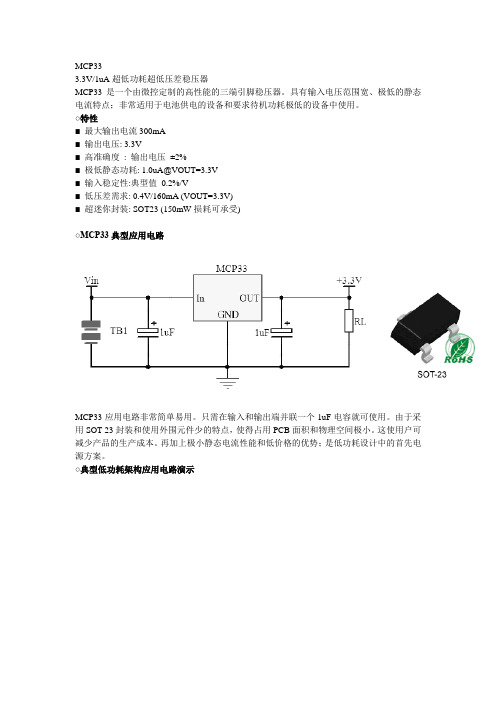
MCP333.3V/1uA超低功耗超低压差稳压器MCP33是一个由微控定制的高性能的三端引脚稳压器。
具有输入电压范围宽、极低的静态电流特点;非常适用于电池供电的设备和要求待机功耗极低的设备中使用。
○特性■ 最大输出电流300mA■ 输出电压: 3.3V■ 高准确度: 输出电压±2%■ 极低静态功耗: 1.0uA@VOUT=3.3V■ 输入稳定性:典型值0.2%/V■ 低压差需求: 0.4V/160mA (VOUT=3.3V)■ 超迷你封装: SOT23 (150mW损耗可承受)○MCP33典型应用电路MCP33应用电路非常简单易用。
只需在输入和输出端并联一个1uF电容就可使用。
由于采用SOT-23封装和使用外围元件少的特点,使得占用PCB面积和物理空间极小。
这使用户可减少产品的生产成本。
再加上极小静态电流性能和低价格的优势;是低功耗设计中的首先电源方案。
○典型低功耗架构应用电路演示上图是低功耗架构的应用电路演示。
电源采用电池供电,电压在3.4V-12V之间。
电源的负载分别有高压部分(相对3.3V而言)和低压部分;高压部分可能应用于一些传感器及模拟前端之类的电路使用。
这部分只有在执行时才由MCU控制开关(SW)提供高压供电,而平时高压电路是零功耗的。
同样,低压电路所使用的3.3也是由MCU控制提供。
就这样,在设备系统待机时MCU将所有外部的电路供电关闭,MCU同时也处于低功耗模式状态。
这样使用设备的整机功耗只有MCU自身的待机电流+MCP33的自身静态电流所决定了。
由于MCP33芯片所消耗的电量极低;那么决定功耗的重任则落在MCU的责任和电路的设计上了。
上图是一个利用太阳能光电板+锂电池+MCP33构成不间断的低功耗电源系统。
太阳能光电板从光/伏转换成微量的电能,经由充电电路变换成直流输出并对锂进行充电。
同时也供MCP33提供电压输入,MCP33输出3.3V电压供给系统使用。
这样的电路非常适合于低功耗的户外设备中使用,具有环保、高效的特点。
MC33160DWR2资料
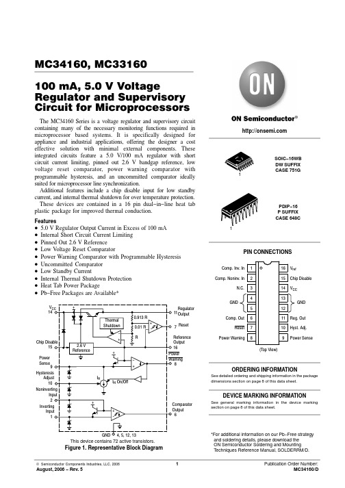
MC34160, MC33160100 mA, 5.0 V VoltageRegulator and Supervisory Circuit for MicroprocessorsThe MC34160 Series is a voltage regulator and supervisory circuit containing many of the necessary monitoring functions required in microprocessor based systems. It is specifically designed for appliance and industrial applications, offering the designer a cost effective solution with minimal external components. These integrated circuits feature a 5.0 V/100 mA regulator with short circuit current limiting, pinned out 2.6 V bandgap reference, low voltage reset comparator, power warning comparator with programmable hysteresis, and an uncommitted comparator ideally suited for microprocessor line synchronization.Additional features include a chip disable input for low standby current, and internal thermal shutdown for over temperature protection.These devices are contained in a 16 pin dual−in−line heat tab plastic package for improved thermal conduction.Features•5.0 V Regulator Output Current in Excess of 100 mA •Internal Short Circuit Current Limiting •Pinned Out 2.6 V Reference •Low V oltage Reset Comparator•Power Warning Comparator with Programmable Hysteresis •Uncommitted Comparator •Low Standby Current•Internal Thermal Shutdown Protection •Heat Tab Power Package•Pb−Free Packages are Available*Figure 1. Representative Block DiagramV1415Power Sense12109This device contains 72 active transistors.See detailed ordering and shipping information in the package dimensions section on page 8 of this data sheet.ORDERING INFORMATION*For additional information on our Pb−Free strategy and soldering details, please download the ON Semiconductor Soldering and Mounting T echniques Reference Manual, SOLDERRM/D.See general marking information in the device marking section on page 8 of this data sheet.DEVICE MARKING INFORMATIONMAXIMUM RATINGSRating Symbol Value Unit Power Supply Voltage V CC40V Chip Disable Input Voltage (Pin 15, Note 1)V CD−0.3 to V CC V Comparator Input Current (Pins 1, 2, 9)I in−2.0 to +2.0mA Comparator Output Voltage (Pins 6, 7, 8)V O40V Comparator Output Sink Current (Pins 6, 7, 8)I Sink10mA Power Dissipation and Thermal CharacteristicsP Suffix, Dual−In−Line Case 648CThermal Resistance, Junction−to−AirThermal Resistance, Junction−to−Case (Pins 4, 5, 12, 13) DW Suffix, Surface Mount Case 751GThermal Resistance, Junction−to−AirThermal Resistance, Junction−to−Case (Pins 4, 5, 12, 13)R q JAR q JCR q JAR q JC80159418°C/WOperating Junction T emperature T J+150°COperating Ambient T emperatureMC34160MC33160T A0 to +70−40 to +85°CStorage T emperature Range T stg−65 to +150°C Stresses exceeding Maximum Ratings may damage the device. Maximum Ratings are stress ratings only. Functional operation above the Recommended Operating Conditions is not implied. Extended exposure to stresses above the Recommended Operating Conditions may affect device reliability.1.The maximum voltage range is −0.3 V to V CC or +35 V, whichever is less.ELECTRICAL CHARACTERISTICS (V CC = 30 V, I O = 10 mA, I ref = 100 m A) For typical values T A = 25°C, for min/max values T A isthe operating ambient temperature range that applies [Notes 2 and 3], unless otherwise noted.)Characteristics Symbol Min Typ Max Unit REGULATOR SECTIONT otal Output Variation (V CC = 7.0 V to 40 V, I O = 1.0 mA to 100 mA, T A = T low to T high)V O 4.75 5.0 5.25V Line Regulation (V CC = 7.0 V to 40 V, T A = 25°C)Reg line− 5.040mV Load Regulation (I O = 1.0 V to 100 mA, T A = 25°C)Reg load−2050mV Ripple Rejection (V CC = 25 V to 35 V, I O = 40 mA, f = 120 Hz, T A = 25°C)RR50 6.5−dB REFERENCE SECTIONT otal Output Variation (V CC = 7.0 to 40 V, I O = 0.1 mA to 2.0 mA, T A = T low to T high)V ref 2.47 2.6 2.73V Line Regulation (V CC = 5.0 V to 40 V, T A = 25°C)Reg line− 2.020mV Load Regulation (I O = 0.1 mA to 2.0 mA, T A = 25°C)Reg load− 4.030mV RESET COMPARATORThreshold Voltage High State Output (Pin 11 Increasing)Low State Output (Pin 11 Decreasing)Hysteresis V IHV ILV H−4.550.02(V O−0.11)(V O−0.18)0.07(V O−0.05)−−VOutput Sink Saturation (V CC = 4.5 V, I Sink = 2.0 mA)V OL−−0.4V Output Off−State Leakage (V OH = 40 V)I OH−− 4.0m A POWER WARNING COMPARATORInput Offset Voltage V IO− 1.210mV Input Bias Current (V Pin9 = 3.0 V)I IB−−0.5m AInput Hysteresis Current (V Pin9 = V ref − 100 mV)R Pin10 = 24 kR Pin10 = ∞I H404.5507.56011m AOutput Sink Saturation (I Sink = 2.0 mA)V OL−0.130.4V Output Off−State Leakage (V OH = 40 V)I OH−− 4.0m A 2.T lo=0°C for MC34160T high=70°C for MC34160−40°C for MC3316085°C for MC331603.Low duty cycle pulse testing techniques are used during test to maintain junction temperature as close to ambient as possible.ELECTRICAL CHARACTERISTICS (continued) (V CC = 30 V, I O = 10 mA, I ref = 100 m A) For typical values T A = 25°C, for min/maxvalues T A is the operating ambient temperature range that applies [Notes 4 and 5], unless otherwise noted.)CharacteristicsSymbolMinTypMaxUnitUNCOMMITTED COMPARATORInput Offset Voltage (Output Transition Low to High)V IO −−20mV Input Hysteresis Voltage (Output Transition High to Low)I H 140200260mV Input Bias Current (V Pin 1, 2 = 2.6 V)I IB −−−1.0m A Input Common Mode Voltage Range V ICR 0.6 to 5.0−−V Output Sink Saturation (I Sink = 2.0 mA)V OL −0.130.4V Output Off−State Leakage (V OH = 40 V)I OH−−4.0m ATOTAL DEVICEChip Disable Threshold Voltage (Pin 15)High State (Chip Disabled)Low State (Chip Enabled)V IH V IL 2.5−−−−0.8V Chip Disable Input Current (Pin 15)High State (V in = 2.5 V)Low State (V in = 0.8 V)I IH I IL −−−−10030m A Chip Disable Input Resistance (Pin 15)R in 50100−k W Operating Voltage Range V O (Pin 11) Regulated V ref (Pin 16) RegulatedV CC 7.0 to 405.0 to 40−−−−V Power Supply Current Standby (Chip Disable High State)Operating (Chip Disable Low State)I CC−−0.181.50.353.0mA4.T lo =0°C for MC34160T high =70°C for MC34160−40°C for MC3316085°C for MC331605.Low duty cycle pulse testing techniques are used during test to maintain junction temperature as close to ambient as possible.Δ, R E G U L A T O R O U T P U T V O L T A G E C H A N G E (m VO V Figure 4. Reference Output Voltage Changeversus Source CurrentFigure 5. Power Warning Hysteresis Currentversus Programming ResistorI ref , REFERENCE OUTPUT SOURCE CURRENT (mA)Δ, R E F E R E N C E O U T P U T V O L T A G E C H A N G E (m V )r e f 02.0 4.0 6.08.0V R H , PROGRAMMING RESISTOR (kW)20406080100120140Figure 8. Comparator Output Saturationversus Sink CurrentFigure 9. P Suffix (DIP−16) Thermal Resistance andMaximum Power DIssipation versusP .C.B. Copper Length, O U T P U T D E L A Y T I M E (n s )D L Y t I Sink , SINK CURRENT (mA), O U T P U T S A T U R A T I O N (V )O L 0.50.40.30.20.100 2.0 4.06.08.0V L, LENGTH OF COPPER (mm), θJ A R Figure 10. DW Suffix (SOP−16L) Thermal Resistance and Maximum Power Dissipation versus P .C.B. Copper Length3040506070809000.40.81.21.62.02.402030504010L, LENGTH OF COPPER (mm)100 2.8P D R , T H E R M A L R E S I S T A N C EJ A θJ U N C T I O N -T O -A I R ( C /W )°, M A X I M U M P O W E R D I S S I P A T I O N (W )PIN FUNCTION DESCRIPTIONPin Function Description1Comparator InvertingInput This is the Uncommitted Comparator Inverting input. It is typically connected to a resistor divider to monitor a voltage.2Comparator NoninvertingInput This is the Uncommitted Comparator Noninverting input. It is typically connected to a reference voltage.3N.C.No connection. This pin is not internally connected.4, 5, 12, 13GND These pins are the control circuit grounds and are connected to the source and load groundreturns. They are part of the IC lead frame and can be used for heatsinking.6Comparator Output This is the Uncommitted Comparator output. It is an open collector sink−only output requiringa pullup resistor.7Reset This is the Reset Comparator output. It is an open collector sink−only output requiring apullup resistor.8Power Warning This is the Power Warning Comparator output. It is an open collector sink−only outputrequiring a pullup resistor.9Power Sense This is the Power Warning Comparator noninverting input. It is typically connected to aresistor divider to monitor the input power source voltage.10Hysteresis Adjust The Power Warning Comparator hysteresis is programmed by a resistor connected from thispin to ground.11Regulator Output This is the 5.0 V Regulator output.14V CC This pin is the positive supply input of the control IC.15Chip Disable This input is used to switch the IC into a standby mode turning off all outputs.16V ref This is the 2.6 V Reference output. It is intended to be used in conjunction with the PowerWarning and Uncommitted comparators.OPERATING DESCRIPTIONThe MC34160 series is a monolithic voltage regulator and supervisory circuit containing many of the necessary monitoring functions required in microprocessor based systems. It is specifically designed for appliance and industrial applications, offering the designer a cost effective solution with minimal external components. These devices are specified for operation over an input voltage of 7.0 V to 40 V, and with a junction temperature of −40° to +150°C. A typical microprocessor application is shown in Figure 11. RegulatorThe 5.0 V regulator is designed to source in excess of 100mA output current and is short circuit protected. The output has a guaranteed tolerance of ±5.0% over line, load, and temperature. Internal thermal shutdown circuitry is included to limit the maximum junction temperature to a safe level. When activated, typically at 170°C, the regulator output turns off.In specific situations a combination of input and output bypass capacitors may be required for regulator stability. If the regulator is located an appreciable distance (≥4″) from the supply filter, an input bypass capacitor (C in) of 0.33 m F or greater is suggested. Output capacitance values of less than 5.0 nF may cause regulator instability at light load (≤1.0 mA) and cold temperature. An output bypass capacitor of 0.1 m F or greater is recommended to ensure stability under all load conditions. The capacitors selected must provide good high frequency characteristics.Good construction techniques should be used to minimize ground loops and lead resistance drops since the regulator does not have external sense inputs. ReferenceThe 2.6 V bandgap reference is short circuit protected and has a guaranteed output tolerance of ±5.0% over line, load, and temperature. It is intended to be used in conjunction with the Power Warning and Uncommitted comparator. The reference can source in excess of 2.0 mA and sink a maximum of 10 m A. For additional current sinking capability, an external load resistor to ground must be used.Reference biasing is internally derived from either V CC or V O, allowing proper operation if either drops below nominal.Chip DisableThis input is used to switch the IC into a standby mode. When activated, internal biasing for the entire die is removed causing all outputs to turn off. This reduces the power supply current (I CC) to less than 0.3 mA.ComparatorsThree separate comparators are incorporated for voltage monitoring. Their outputs can provide diagnostic information to the microprocessor, preventing system malfunctions.The Reset Comparator Inverting Input is internally connected to the 2.6 V reference while the Noninverting Input monitors V O . The Reset Output is active low when V O falls approximately 180 mV below its regulated voltage. To prevent erratic operation when crossing the comparator threshold, 70mV of hysteresis is provided.The Power Warning Comparator is typically used to detect an impending loss of system power. The Inverting Input is internally connected to the reference, fixing the threshold at 2.6 V . The input power source V in is monitored by the Noninverting Input through the R 1/R 2 divider (Figure 11). This input features an adjustable 10 m A to 50m A current sink I H that is programmed by the value selected for resistor R H . A default current of 6.5 m A is provided if R H is omitted. When the comparator input falls below 2.6V , the current sink is activated. This produces hysteresis if V in is monitored through a series resistor (R 1). The comparator thresholds are defined as follows:R1R 21 +− I IB R 1V th(lower) = V ref R1R 21 ++ I H R 1V th(upper) = V refThe nominal hysteresis current I H equals 1.2 V/R H (Figure 5).The Uncommitted Comparator can be used to synchronize the microprocessor with the ac line signal for timing functions, or for synchronous load switching. It can also be connected as a line loss detector as shown in Figure 12. The comparator contains 200 mV of hysteresis preventing erratic output behavior when crossing the input threshold.The Power Warning and Uncommitted Comparators each have a transistor base−emitter connected across their inputs. The base input normally connects to a voltage reference while the emitter input connects to the voltage to be monitored. The transistor limits the negative excursion on the emitter input to − 0.7 V below the base input by supply current from V CC . This clamp current will prevent forward biasing the IC substrate. Zener diodes are connected to the comparator inputs to enhance the ICs electrostatic discharge capability. Resistors R 1 and R in must limit the input current to a maximum of ±2.0mA.Each comparator output consists of an open collector NPN transistor capable of sinking 2.0 mA with a saturation voltage less than 0.4 V , and standing off 40 V with minimal leakage. Internal bias for the Reset and Power Warning Comparators is derived from either V CC or the regulator output to ensure functionality when either is below nominal.Heat Tab PackageThe MC34160 is contained in a 16 lead plastic dual−in−line package in which the die is mounted on a special Heat Tab copper alloy lead frame. This tab consists of the four center ground pins that are specifically designed to improve thermal conduction from the die to the surrounding air. The pictorial in Figure 9 shows a simple but effective method of utilizing the printed circuit board medium as a heat dissipator by soldering these tabs to an adequate area of copper foil. This permits the use of standard board layout and mounting practices while having the ability to more than halve the junction to air thermal resistance. The example and graph are for a symmetrical layout on a single sided board with one ounce per square foot copper.AC Figure 11. Typical Microprocessor ApplicationFigure 12. Line Loss Detector ApplicationLine Loss OutputV refMPU ResetV O Pin 6Pin 8Point A Figure 13. Time Delayed Microprocessor ResetrefV OV inMPU ResetORDERING INFORMATIONDevice Operating Temperature Range Package Shipping†MC34160DWT A = 0° to +70°CSOIC−16WB47 Units / RailMC34160DWG SOIC−16WB(Pb−Free)47 Units / RailMC34160DWR2SOIC−16WB1000 Units / T ape & Reel MC34160DWR2G SOIC−16WB(Pb−Free)1000 Units / T ape & Reel MC34160P PDIP−1625 Units / RailMC34160PG PDIP−16(Pb−Free)25 Units / RailMC33160DWT A = −40° to +85°C SOIC−16WB47 Units / RailMC33160DWG SOIC−16WB(Pb−Free)47 Units / RailMC33160DWR2SOIC−16WB1000 Units / T ape & ReelMC33160DWR2G SOIC−16WB(Pb−Free)1000 Units / T ape & ReelMC33160P PDIP−1625 Units / RailMC33160PG PDIP−16(Pb−Free)25 Units / Rail†For information on tape and reel specifications, including part orientation and tape sizes, please refer to our Tape and Reel Packaging Specifications Brochure, BRD8011/D.MARKING DIAGRAMS161 MC3x160= Device CodeDW = SOIC−16P = PDIP−16x = 4 or 3A= Assembly Location WL= Wafer LotYY= YearWW= Work WeekG= Pb−Free PackageMC3x160P AWLYYWWG PDIP−16SOIC−16WBPACKAGE DIMENSIONSSOIC−16 WBDW SUFFIXPLASTIC PACKAGECASE 751G−03ISSUE Cq NOTES:1.DIMENSIONS ARE IN MILLIMETERS.2.INTERPRET DIMENSIONS AND TOLERANCESPER ASME Y14.5M, 1994.3.DIMENSIONS D AND E DO NOT INLCUDEMOLD PROTRUSION.4.MAXIMUM MOLD PROTRUSION 0.15 PER SIDE.5.DIMENSION B DOES NOT INCLUDE DAMBARPROTRUSION. ALLOWABLE DAMBARPROTRUSION SHALL BE 0.13 TOTAL INEXCESS OF THE B DIMENSION AT MAXIMUMMATERIAL CONDITION.DIM MIN MAXMILLIMETERSA 2.35 2.65A10.100.25B0.350.49C0.230.32D10.1510.45E7.407.60e 1.27 BSCH10.0510.55h0.250.75L0.500.90q0 7 __PACKAGE DIMENSIONSPDIP−16P SUFFIXPLASTIC PACKAGE CASE 648C−04ISSUE DAM0.005 (0.13)T ON Semiconductor and are registered trademarks of Semiconductor Components Industries, LLC (SCILLC). SCILLC reserves the right to make changes without further notice to any products herein. SCILLC makes no warranty, representation or guarantee regarding the suitability of its products for any particular purpose, nor does SCILLC assume any liability arising out of the application or use of any product or circuit, and specifically disclaims any and all liability, including without limitation special, consequential or incidental damages. “Typical” parameters which may be provided in SCILLC data sheets and/or specifications can and do vary in different applications and actual performance may vary over time. All operating parameters, including “Typicals” must be validated for each customer application by customer’s technical experts. SCILLC does not convey any license under its patent rights nor the rights of others. SCILLC products are not designed, intended, or authorized for use as components in systems intended for surgical implant into the body,or other applications intended to support or sustain life, or for any other application in which the failure of the SCILLC product could create a situation where personal injury or death may occur. Should Buyer purchase or use SCILLC products for any such unintended or unauthorized application, Buyer shall indemnify and hold SCILLC and its officers, employees,subsidiaries, affiliates, and distributors harmless against all claims, costs, damages, and expenses, and reasonable attorney fees arising out of, directly or indirectly, any claim of personal injury or death associated with such unintended or unauthorized use, even if such claim alleges that SCILLC was negligent regarding the design or manufacture of the part.SCILLC is an Equal Opportunity/Affirmative Action Employer. This literature is subject to all applicable copyright laws and is not for resale in any manner.PUBLICATION ORDERING INFORMATION。
挤出空间、降低成本:从 MCP、eMCP 与 eMMC 看移动设备内存的整合
挤出空间、降低成本:从MCP、eMCP 与eMMC 看移动设备内存的整合智能手机与平板电脑等移动设备蓬勃发展,性能好坏与否,除了好的CPU,内存的搭配也成了重要关键,随着技术的发展日臻成熟,移动设备得以衍生出不同等级的产品,以贴合不同消费者的需求,CPU 有低中高端之分,内存也有所谓内存阶层的概念(Memory hierarchy),要让储存容量、运算速度、单位价格等相异的多种内存妥善分配,达到最大经济效益。
手机与平板电脑等移动设备愈发讲求轻薄甚至小巧,成了厂商构装的难题,为了节省空间,将多重芯片放入单一构装成了各家厂商努力的重点,RAM 与ROM 的整合与封装也成了其一。
技术的发展,使得RAM 与ROM 两者可整合为一,甚至可以直接内建控制芯片,为手机制造商节省了成本或生产上的困扰。
以下以智能手机内存常见的配置方式为例,阐述移动设备内存整合的演进。
MCP──内存整合的滥觞MCP 为Multi Chip Package 多晶片封装的简称,是将两种以上的内存芯片透过水平放置或堆叠的方式成同一个BGA 封装,MCP 合而为一的方式,较以往以主流TSOP 封装成单独两个芯片,节省70% 的空间,简化了PCB 板的结构,也简化了系统设计,使得组装与测试良率得以提高。
一般MCP 组合方式有两种:一为NOR Flash 加Mobile DRAM(SRAM 或PSRAM),一种为NAND Flash 加DRAM 或Mobile DRAM(SRAM 或PSRAM)而NAND Flash 由于储存密度高、功耗低、体积小,成本也较NOR Flash 低廉,以目前基本的1Gb 配置来看,NOR Flash 1Gb 的价格约在6 美元,为相同容量SLC NAND Flash 的六倍,使得NAND 渐有取代NOR 之势。
总体而言,MCP 降低了系统硬件成本,价格甚至比各自独立的芯片还要便宜,MCP 的最终多取决于NAND Flash 价格变化,不过一般而言至少可便宜10% 以上。
DSP系统应用中FLASH在线编程方法
摘 要: 介绍了在TI公司TMS320VC33 DSP应用系统中,通过JTAG口对DSP外部FLASH存储器实现在线编程在线编程的方法,给出了示例源程序,完成了DSP系统加电后的自动装载运行。 关键词: DSP JTAG FLASH存储器 在线编程 Bootload
2 TMS320VC33简介 TMS320VC33是美国TI公司推出的TMS320C3X系列的32位浮点数字信号处理器,它是在TMS320C31浮点DSP的基础上开发的一个价格更低的DSP,该产品具有高速、低功耗、低成本、易于开发等显著优点。TMS320VC33采用内部1.8V,外部3.3V供电,因而它的功耗比原有型号TMS320C31的功耗降低了大约一个数量级,而且能支持高达150M/FLOPS的运行速率。其主要特性如下: CPU是32bit的高性能CPU:可进行16/32b整数和32/40b的浮点操作;内含8个扩展精度寄存器;有2个地址发生器、8个辅助寄存器和2个辅助寄存器算术单元(ARAU)。 片内存储器为32bit指令字、24bit地址线、34K×32b(1.1Mb)的双静态RAM。 外围接口具有启动程序装载功能;内含5倍频的锁相环(PLL)时钟发生器;片内存储器可映射外设,其中包括一个串行口、两个32bit定时器和一个DMA;具有四个内部译码页选,可大大简化TMS320VC33与I/O及存储器的接口。3 TMS320VC33程序引导功能 TMS320VC33具有两种存储器映射方式,即MP(Microprocessor Mode)方式和MC/BL(Microcomputer/Bootloader Mode)方式,两种方式下中断向量的位置不同。常用的是MC方式。在该方式下,MCBL/MP引脚接高电平,内部ROM被映射到000~FFF空间。这段ROM中含有器件生产厂家固化的引导程序引导程序(BootLoader),该引导程序可以将DSP实时运行的程序和数据从外部低速ROM或串行口装入到高速RAM中。 TMS320VC33复位后即运行内部固化的引导程序,引导程序通过查询四个中断引脚来确定装入方式。这些引脚为低电平有效,查询顺序依次为INT3、INT0、INT1、INT2;当INT3有效时,为串行装入方式;当INT0有效时,从外部地址0x001000处装入(BOOT1);当INT1有效时,从外部地址0x400000处装入(BOOT2);当INT2有效时,从外部地址0xfff000处装入(BOOT3)。 TMS320VC33具有四个快速页选信号,用于对外部地址空间寻址,其映射如表2所示。
TMS320VC33系列讲座资料开发技巧
TMS320VC33系列讲座资料第一讲VC33的电源设计这里主要结合实际项目来讲解VC33的最小系统设计,这一讲为电源电路设计,主要分为一下几个部分进行:DSP系统需要的电源种类 DSP系统电源供电的特殊要求:上电次序数字/模拟混合系统电源处理方法电源电路设计及器件选型电源在PCB设计时的一些注意事项1、给TI DSP供电,TI DSP有5类典型电源引脚:CPU核电源引脚,I/O电源引脚PLL电路电源引脚Flash编程电源引脚(仅C2000系列DSP有)模拟电路电源引脚(仅C2000系列DSP有)2、上电次序,CPU内核先于I/O上电,后于I/O掉电(TMS320F281X例外,刚好相反)CPU内核与I/O供电应尽可能同时,二者时间相差不能太长(一般不能>1s,否则会影响器件的寿命或损坏器件)为了保护DSP器件,应在内核电源与I/O电源之间加一肖特基二极管3、数字与模拟部分单独供电最后通过磁珠接在一点即可4、电源电路设计主要的考虑因素用哪种类型的电源器件:转换效率、成本和空间,输入电压,输出电压(输出电压是否可调、输出电压的路数)输出电流:控制/状态:EN控制、PowerGood状态5、电源器件选型,这里列出一些常用的LDO,供大家在设计时选择双路输出输入电压输出电压输出电流辅助功能TPS767D318: 5V 3.3V/1.8V 1A/1A ENTPS767D301: 5V 3.3V/可调 1A/1A EN单路输出TPS76333: 5V 3.3V 150mA ENTPS76801: 5V 可调 1A EN、PGTPS75701: 5V 可调 3A EN、PGTPS75501: 5V 可调 5A EN、PG我在做VC33设计中用到的电源器件是双路输出的TPS767D318。
实际中的连接电路大家可以参照Datasheet。
6、电源在PCB时的注意事项:数字地、模拟地分开,单点连接,强烈推荐采用多层板,为电源和地分别安排专用的层。
dsPIC33C数字信号控制器设计指南说明书
A Leading Provider of Smart, Connected and Secure Embedded Control SolutionsdsPIC33C Digital Signal ControllerDesign GuidelinesdsPIC33C Digital Signal ControllersGeneric Robust GuidelineRobustness features on dsPIC33C DSCs•Internal regulator is Capacitor-less design•No need of an external capacitor, no noise injection from the board•Saves space on the board for routing•Lower component count, lower cost•One extra I/O pin•Virtual Pins for Redundancy and Monitoring : Dual core device feature to cross check/monitor •Flash ECC (Error Correcting Code):Flash Error check with 1-bit detection/correction & 2-bit detection •DMT (Deadman Timer) : Instruction cycle counting and could be used as a SW checkpoint•WDT (Watchdog Timer) : For system recovery•CodeGuard™Security : For code protection schemes•CRC (Cyclic Redundancy Check) : For code validation•Two-Speed Start-up : For slow start up from power on, reduce inrush current•Fail-Safe Clock Monitoring : Clock monitor and switch•Backup FRC (BFRC) : Backup for the FRC clock•AEC-Q100 REVG (Grade 0: -40°C to +150°C) Compliant : Automotive QualDecoupling Capacitor•For wide frequency noise filtering, provide multiple decoupling capacitors (e.g.0.01uF,0.1uF) across supply pins of dsPIC33C DSC •When multiple capacitors are provided, place them in ascending order of their value with lowest value capacitor closest to the dsPIC33C pin •Provide decoupling capacitors between each VDD/GND pair of the dsPIC33C DSC •Place decoupling capacitors close to VDD and GND pin pairs of the dsPIC33C DSC•Connect dsPIC33C DSC pin and capacitor pads using shorter directtraces without any vias between them•Also connect decoupling capacitor between AVDD and AGNDusing shorter tracesDecoupling Caps :AVDD -AGND Decoupling Caps : DVDD -DGNDOscillator and MCLR•Place crystal oscillator close to OSCI/OSCO pins ofthe dsPIC33C DSC and connect it using short directtraces avoiding vias•Provide isolated ground plane under the crystal,connect this ground Isle to Board Ground•Avoid any high-speed signals running near theoscillator circuit•Add series resistor between reset pushbutton andMCLR pin of the dsPIC33C DSCsCurrent feedbacksFrom shunt to amplifier inputs•Use Kelvin sensing –take separate tracesfrom pads of the shunt resistor forconnecting to amplifier input resistors•Take the current feedbacks traces fromshunt resistor as differential pair runningparallel across the board until it isconnected to amplifier input resistors(which are placed closer to amplifierpositive and negative input pins)Ground Connection Analog and Digital Ground•Separate the ground of digital circuits, analog circuits ,high speed circuit, high current circuit etc.•The separated ground must be connected only at supply start point which is closer to the 3.3V LDO (dsPIC33C DSC Supply)•In case of multilayer board, dedicate at least one internal layer for grounds. Try to provide solid ground plane avoiding any cuts •To do this , it is necessary to identify the components that connect to specific ground and place them close to each other in specific area of the boardExample :Solid internal AnalogGround(AGND) planejoining at LDO ground.Digital Ground (DGND) trace Analog Ground (AGND) traceAGND and DGND are joined at one point near the source using net tie.Low Noise GuidelineWeak Spot ADCAnalog-To-Digital Converter Circuit•Increasing CPU speed with shrinking structure sizes result in an increased sensitivity to noise•CPU load transient frequencies stimulate passive/reactive circuits formed by parasitic RLC resonators (PCB)•Digital high-speed peripherals add to noise level•In control applications, the ADC is the most sensitive element and provides the guiding value for noise budget estimations •Power Electronics Control Applications are most sensitive to ADC accuracy•Limited Resolution limits dynamic range of control loop •Noise on feedback signal reproduces on ADC results •Noise on supply lines influences internal references •Faster ADCs generate more noise within the internal, analog circuit DIGITIZEDBLOCK ADC Power Stage(Plant)Error Amplifier +–PWM (Modulator)VoltageDividerREF V ERROR REF OUT V V K V =−⋅EA V D K OUTV INVNoise BudgetHow much noise is acceptable?•Determine maximum acceptable voltage deviation •The most system element influencing the most sensitive parameter of the product determines the acceptance level •In power conversion, this is output voltage / output current accuracy and response characteristic •Both highly depend on reliable ADC results Power ConverterCircuitV IN V OUTADC REF V FBerror+-H C z(Compensator)outputinput Anti-WindupPWMNoise Budget –Potential Noise SourcesHow much noise is acceptable?•Noise can influence the ADC through 3 major ports•(A) Feedback Noise via Input Pin •(B) Ground Noise / Bouncing•(C) Reference Voltage derived from Supply Voltage•Noise can inject•Alias frequencies•Random, erroneous samples•Decrease effective ADC resolution•Maximum acceptable noise levels are application dependent and need to be derived individuallyV FBV F B (t ) ± VTimeFeedbackV o u t [n ]n →InputCLOCKAVSSAVDDV REFABCThree Major Noise PortsADCAlias Frequencies•Random noise on feedback signals are relatively uncritical•Periodic noise components exceeding the minimum ADC granularity may influence ADC results •If these are at around or higher than f SAM /2, alias-frequencies may be injected•High-speed ADCs with very small Sample & Hold (S&H)•Capacitance and short sampling times are getting increasingly sensitive to periodic noise on feedback signals •Once alias frequencies have been injected in the data stream, they may influence the control system.•Recommended to add anti-alias filters to input pins, tuned for the effective sampling frequency of the application while still allowing relevant transients to pass.-1.5-1-0.500.511.504590135180225270315360Waveform Sampled at f NFeedback Sampled InputM a g n i t u d ef SAM 2f SAM70k H z40k H z30k H z 25k H z 10k H z160k H z510k H zI n p u t F r e q u e n c yI n p u t F r e q u e n c yI n p u t F r e q u e n c yAnti-Alias Filter DesignAdjustment of anti-alias cut-off frequencies need to consider the internal ADC architecture to prevent excessive ADC result deviations•Shared ADC CoresADC cores with multiple analog input pins (ANx) connect the single S&H capacitor to the pin via multiplexers. To prevent cross-talkbetween input channels, the S&H capacitor needs to be discharged before connection. When connected, the S&H capacitor needsenough time to charge up to the feedback voltage level to achievean accurate result.•Dedicated ADC CoresDedicated cores continuously keep their S&H connected to the pin, tracking the feedback voltage. The connection is only opened during conversion and closed when conversion has completedADCV FB*V FBCAnti-Alias Filter Design / Shared ADC Core•Step 1: Decoupling Capacity•During sampling using the shared ADC core, the discharged S&H capacitor C HOLD is connected to the feedback circuit. C HOLD is charged through R SS and R IC (~350 W ). The high charging current right after SW SS is closed injects a fast transient into the feedback line. Depending on the distance between the voltage divider and the device input pin, the parasitic trace inductance might prevent to bias this inrush current. Hence, this current is exclusively biased by decoupling capacitor C , eventually forming a capacitive voltage divider with C HOLD . As a result, the final sampling voltage will always settle below the real feedback voltage V FB introducing a measurement error ofError = 1−C HOLD C(first assessment of the static offset)•Software adjustable sampling times allow accounting for and thus minimizing these effects which, however , increases the data acquisitionlatency. For high-speed designs it is therefore recommended to minimize the static error by placing enough capacitance as close as possible at the ADC input pin (recommended value = 30…50 x C HOLD ).V FB *V FBCRV OUTC PINC HOLDV DDR ICR SSSampling Switch I LEAKAGESL TRACEParasitic Trace InductanceC DR BSW SSAnti-Alias Filter Design / Shared ADC Core•Step 2: Filter Resistor•Peak-to-Peak voltage levels of periodic noise should be limited to the voltage equivalent of approx. 3 LSB. At V REF = 3.3V and 12-bit resolution the ADC has a total granularity of 806 µV/tick. 3 LSB therefore have a voltage equivalent of 6.44 mV . The total acceptable level,however , depends on the total feedback signal range and needs to be calculated for every application individually.Example:•A signal is sampled at f SAM = 500 kHz (Nyquist-Shannon limit at f N = 250 kHz). A dominant, periodic noise component f Noise = 1000 kHz with a max. deviation of V Noise pk-pk = 60mV is observed. To prevent alias frequencies being injected into the ADC data stream, this noise needs to be damped to less than 6.44 V @ f N .(-20dB @ f N = 6 mV). The pole introduced by the RC filter therefore needs to be placed one magnitude below f N (=25 kHz) to effectively damp the noise magnitude at f N by factor 10.V FB *V FBCRV OUTC PINC HOLDV DDDistance XR ICR SSSampling SwitchI LEAKAGESL TRACEParasitic Trace InductanceC DR AR BSW SSAnti-Alias Filter Design / Shared ADC Core•Step 3: Recharging Decoupling Capacitor C•After the sampling transient has passed, decoupling capacitor C needs to be recharged up to the feedback level for the next sample. With high resistive voltage divider networks, it is recommended to place an additionaldecoupling capacitor in parallel to the lower voltage divider resistor. This capacitor also helps to compensate the parasitic trace inductance L TRACE . At high sampling frequencies hand high resistive voltage dividers an operational amplifier might be required to recharge C in time for the next sample.V FB *V FBCRV OUTC PINC HOLDV DDDistance XR ICR SSSampling Switch I LEAKAGESL TRACEParasitic Trace Inductance C DR AR BSW SSAnti-Alias Filter Design / Shared ADC Core•Design Tip:•Power electronics designs are commonly noisy as the circuit itself produces noise over a very wide frequency range up to manyGHz. Dominant noise bands in the range of 8-15 MHz caused by Diode ringing as well as harmonics of the switching frequency are sometimes difficult to contain and might be induced in feedback lines. The magnitude of the induced noise is independent from the voltage level present.•Hence, it is recommended to place the voltage divider close to the device, minimizing Distance X as well as the parasitic trace inductance L TRACE . Especially, however, preventing noise from being induced in low voltage signals. Noise induced on high voltage signals will get divided with the feedback signal and will therefore have lower amplitudes requiring less damping and thus expanding the maximum bandwidth of the feedback signal.V FB *V FBCRV OUTC PINC HOLDV DDR ICR SSSampling Switch I LEAKAGESL TRACEParasitic Trace Inductance C DR AR BSW SSNoise Budget –Potential Noise SourcesHow much noise is acceptable?•In addition to adjust noise filtering on feedback signals, it is required to analyze the noise floor on supply and ground lines•The ADC uses a reference voltage, which is derived from the supply voltage•Noise on this supply rail can influence the reference level during a conversion process, equally perturbing ADC results as sampling noisy signals.•Supply rain noise can enter the system through VDD as well as through VSSV FBB (t ) ± VFeedbackV o u t [n ]n →InputCLOCKAVSSAVDDV REFABCADCSymmetrical Layout•The CPU itself is a potential noise hub in the system. Each instruction executed by the CPU will create a load step with low amplitude but high edge speed. These high frequency current pulses are exclusively biased by the decoupling capacitors. The generated AC noise inevitably migrates into supply and ground traces, forward into the device as well as backwards to the voltage regulator (VRM).•Insufficient decoupling can stimulate passive/reactive elements along the way, which, if stimulated in the right frequency, may start to resonate, increasing the noise level.FBVDD/VSSANALOG INPUTSCDLOADVoltage Regulator Module (VRM)Passive/Reactive NetworkActive NetworkVREFC DAB dsPIC33C DSCCCCDigital GroundAnalog GroundOESRC ESLL O A DI LI ESLV DDV SSSymmetrical LayoutFour resonant peaks were found withinthe relevant frequency bandVDD Impedance profile measured at every decoupling capacitor(unpowered and powered)dsPIC33 Target ImpedanceHighly reactive resonance valleysI m p e d a n c e M a g n i t u d eSymmetrical Layout dsPIC33TargetImpedancewindow of interest Stimulus windowTotal VDD Impedance profile measured at PDN Port BCPU Clock Frequencies f CY2f CY f OSCKey Takeaways•Key Takeaways•Sharp valleys in an impedance profile indicate the presence of resonance/anti-resonance frequencies of passive/reactive network elements•The CPU load profile is determined by instruction execution and peripheral activity, which are both software dependent to a high degree•The faster the CPU, the wider the frequency range across potential stimuli can be injected into the passive/reactive network segment•If one or more resonators are stimulated simultaneously, the noise level may inflationary increase (Rouge Wave)•Remedy: Flat Impedance Design•Output impedance of voltage regulator must match target impedance•Decoupling capacitors must be selected to match/cancel excess inductance (traces)•Symmetrical design (equal trace length and width of VDD lines reduce number of resonant peaks)•Using ground planes instead of traces reduce VSS trace impedance, shifting potential resonant peaks into high frequency range beyond the Window Of InterestPlease note:Although passive/reactive network components may still be stimulated by higherfrequencies within the Stimulus Window, the CPU won’t be able to pick them up.Noise Budget –Target ImpedanceFlat Impedance Design•Determining Target Impedance Z TARGET•Determine max. acceptable voltage deviation for the application•ADC being the most sensitive element (ADC sample tolerance, e.g.10mV)•Determine minimum and maximum load current, depending on CPU speed and peripheral usage (e.g.I min= 40mA, I max= 80mA)Example:minmaxarg IIToleranceVZ DDetT−⨯=Z T arg et=3.3V×0.010V0.080A−0.040A=0.825WExcess Impedance Cancellation •Positive supply traces (V DD ) between PDN port (B) anddecoupling ports (C) should be as symmetrical as possible toprevent potential resonant frequencies spreading intomultiple peaks concentrated in a narrow frequency range.•Decoupling capacitance need to be selected to cancel the excess inductance of the supply traces. Too much or less capacitance will inevitably result in resonant tank becomingreactive to stimuli. A symmetrical design will allow to use thesame capacitance at every decoupling point (C)•Analog supply voltage is best taken from the nearest decoupling point (C) being filtered through a ferrite bead (E)FB VDD/VSS ANALOG INPUTSCD C C C D O EExcess Impedance Cancellation •Using ground planes instead of traces lowers the excess inductance, effectively moving potential resonant frequencies to higher ranges and eventually out of the Window Of Interest •Digital and analog ground should always be separated preventing noise produced by the CPU entering sensitive analog circuits •Prevent ground planes from overlapping and accidentally coupling noise between planes •Ground decoupling can be done by•Plane gaps, introducing a slightly increased resistance and inductance between both planes limiting noise from migrating•Putting 0 W resistors in between planes introducing the package inductance as a filter barrier•Replacing 0 W resistors by ferrite beads for a more specific filter characteristicFB VDD/VSS ANALOG INPUTS C D CC C Digital GroundAnalog Ground E 0R 0RAnalog Rail DecouplingVDD-2-AVDD Filtering •Digital noise generated by the CPU on V DD gets contained within the network segment by putting up a barrier between V DD and AV DD :•Ferrite Beads allow selective filtering of frequency bands while ensuring proper balancing of decoupling capacitors on V DD and AV DD (recommended)•Low Resistance Resistors also introduce some small package inductance as well provide resistance adding to lowering the Q resp. increase damping (e.g.4.7 W ) •Gapping of layout traces will have similar effects like the options above, but their effectiveness is questionable (not recommended in general) FB VDD/VSSANALOG INPUTS CD CC C Digital GroundAnalog Ground EV SS AV SSFBV DD AV DD 0RAdditional Design GuidanceDesign Example & DocumentsdsPIC33C DSC Design Reference:dsPIC33CH512MP506 Digital Power Plug-In Module (DP-PIM),Part-No. MA330049Anti-Alias Filter Design Guidance:dsPIC33CH512MP506 DP-PIM User Guide /Appendix C. Characterization Data。
TMS320VC33资料

TMS320VC33 DIGITAL SIGNAL PROCESSOR
SPRS087E − FEBRUARY 1999 − REVISED JANUARY 2004
D High-Performance Floating-Point Digital
Signal Processor (DSP): − TMS320VC33-150 − 13-ns Instruction Cycle Time − 150 Million Floating-Point Operations Per Second (MFLOPS) − 75 Million Instructions Per Second (MIPS) − TMS320VC33-120 − 17-ns Instruction Cycle Time − 120 MFLOPS − 60 MIPS 34K × 32-Bit (1.1-Mbit) On-Chip Words of Dual-Access Static Random-Access Memory (SRAM) Configured in 2 × 16K Plus 2 × 1K Blocks to Improve Internal Performance x5 Phase-Locked Loop (PLL) Clock Generator Very Low Power: < 200 mW @ 150 MFLOPS 32-Bit High-Performance CPU 16- / 32-Bit Integer and 32- / 40-Bit Floating-Point Operations Four Internally Decoded Page Strobes to Simplify Interface to I/O and Memory Devices Boot-Program Loader EDGEMODE Selectable External Interrupts 32-Bit Instruction Word, 24-Bit Addresses Eight Extended-Precision Registers
PMDG 777-200 教程 1 中文版

PMDG 777-200LR/F教程1由SinoFSX abccsss / SINO7308翻译目录目录 (2)介绍 (3)概述 (4)地景插件 (4)飞行计划 (4)FSX设置 (5)选择飞机 (5)选择机场 (5)设置时间 (5)设置天气 (5)关于燃油和配载 (6)进入虚拟座舱 (6)飞机设置 (7)燃油和配载设置 (8)关于重量单位 (9)设置FMC航路 (14)位置初始化 (14)输入机场 (16)离场程序输入 (17)输入航路 (19)输入进场和进近程序 (21)航线激活 (25)设置性能数据和垂直航径 (26)设置起飞数据和推力 (29)驾驶舱起飞准备 (32)设置MCP (33)设置EFIS (35)设置顶板 (37)电子检查单......................................... 38 起飞和爬升. (41)起飞 (41)爬升 (44)巡航 (47)延程飞行 (47)PMDG自动巡航功能 (51)下降和进近 (53)下降 (53)最后进近 (60)着陆 (64)附录1 关车和停车程序 (66)着陆后程序 (66)关车程序 (67)停车程序 (70)冷舱 (72)附录2 冷舱启动程序 (73)打开电源 (73)飞行前程序 (74)发动机启动前程序 (77)推出和开车 (78)滑行前程序 (80)结语 (81)译者注:本教程针对的是熟练操作FSX默认机和任务的新手,不需要精通插件机,也花了大量笔墨讲述插件机各种基本原理,并没有涉及很标准的程序。
如果读者有插件机的基础,那么就会觉得非常简单了。
介绍欢迎来到PMDG 777-200LR/F的第一次教程飞行!这是目前FSX平台上最先进的商用喷气机插件之一。
是时候学习驾驶它了!本教程的内容类似于之前的PMDG 737NGX教程1,并不是一个包含所有真实飞行细节的完全教程,而是一个简单的介绍飞行。
PMDG 777-200LR/F的模拟非常深入和精细,经过几年的飞行之后,你仍然会不断地发现其中的新东西。
微尺寸DSP控制器dsPIC33系列产品介绍说明书

SummaryIn today’s automotive applications, ISO26262 has become a critical element of passenger safety, aselectric and electronic content has rapidly grown within cars and now mobility solutions to a widerextent. To help customers achieve the desired Automotive Safety Integrity Level (ASIL) certification,Microchip’s dsPIC33 family of Digital Signal Controllers (DSCs) is commonly used in digital-power andmotor-control applications for the automotive market including DC/DC systems and On-Board Char-gers (OBC), actuators and also sensors (position, pressure) for which ASIL requirements apply.Select dsPIC33 DSCs are products that contains the “Functional Safety Ready” designation. It has been carefully selected as onethat encompasses the latest features and support collateral available from Microchip, including integrated safety features, safetymanuals, Failure Mode, effect, diagnostic analysis (FMEDA) reports and in some cases, diagnostic software./16bitdsPIC® DSCsdsPIC33 DSCs – Functional Safety ReadyDesigned for Robust End ProductsSafety and Robustness Collateral•Automotive-grade silicon (Q100 qualification, up to Grade 0)• Functional Safety Diagnostic Firmware (with completerequirements mapping, static/dynamic analysis and test reports)• Failure modes, Effects and Diagnostic Analysis report •Functional Safety Manual• MPLAB XC Functional Safety Certified Compilers •MCAL Drivers for AutosarThese collaterals are available under NDA upon request from your local Microchip Sales office.Make your certification process easier and less risky with Microchip high-quality collateral.Applications•On-Board Chargers (OBC)•Battery Management Systems (BMS)•Sensors (position, pressure)SiliconWDTsDiversity ECC ClocksRobust Products: Automotive Quality PPAP , Q100, TS16949Software CPU Self Test Drivers MCAL OSEKCollateral Support Internal and external Tools Assistance with achieving ISO 26262Integrated F/S Hardware Modules Software Librariesavailable Ecosystem of Support Automotive GradeproductsISO 26262ComplianceFMEDA,Saftey ManualTools, MISRA C 2012C Compiler, Diagnostic ToolsSafety and Robustness CapabilitiesThe dsPIC33 family of DSCs provide the following features and capabilities for robust environments:• Hardware functional safety features including but not limited to:• Memory: ECC, CRC, RAM BIST• GPIO: ESD Protection, I/O Port ReadbackThe Microchip name and logo, the Microchip logo, dsPIC and MPLAB are registered trademarks of Microchip Technology Incorporated in the U.S.A. and other countries. All other trademarks mentioned herein are property of their respective companies.© 2019, Microchip Technology Incorporated. All Rights Reserved. 8/19 DS00003193A/16bitfunctionalsafetyDevelopment ToolsMicrochip offers a number of products that enable system-level compliance to functional safety. This means that they have integrated features, qualified test libraries, safety manuals, and FMEDA reports, depending on the standard and the level of safety they support.All these items make it easier to develop applications that conform to the functional safety standards, and thereby reduce the work and cost of the final product compliance. Microchip offers the MPLAB ® XC Compiler, ISO 26262 qualified up to ASIL D.Third Party Developers• LDRA software technology • TÜV SÜD• Other functional safety partnershttps:///design-centers/functional-safety/functional-safety-partnersAdditional Information• Some of these hardware features apply to Class B appli-ance applications. For more information, please visit /classb .• /Functional-safety • /FSR。
DSP 第二章 TMS320VC33的结构
(3)TMS320VC33的读写操作共用一个引 脚,该引脚为输出脚,高电平为读,低电平 为写,任何时候都处于读、写两种状态之 一,多数情况下与外部存取选通信号和页选 通信号配合工作。
C = CMOS E = CMOS EPROM
209、203、 240、241、 242
´F2xx DSP
F = Flash E EP RO M
206、240、 241、243
LC = Low-voltage C M O S (3.3 V)
† TQ FP = Thin Q uad Flat Package
当由0变为1时,DSP由复位向量指定的地址开始执行程序,这里所 述的复位向量也是一种中断向量,而且是中断级别最高的中断向量。
(2)高阻控制信号可以与复位信号配合使用,也可以单独使用,使地址 总线、数据总线和各输出信号处于高阻状态,但应注意与的区别,前者可 以使DSP的所有输出信号均处于高阻状态,而后者只能使主总线接口信号 中的地址线A0~A23、数据线D0~D31、读写控制信号、外部存取选通信 号、页选通信号处于高阻状态;二者的另一个区别是:=0不仅使各种输 出信号处于高阻状态,同时也使DSP的存储器和寄存器的内容丢失,而仅 仅使前述的4 种信号处于高阻的保持状态,不丢失有关的内容。
2.3.3串行口信号
串行口信号共6个,分别对应于6个引脚,这6个引脚构成一个 全双工的串口,即任何时候都可以同时进行数据的接收和发送, 而且接收和发送的数据的字长可以是8位、16位、24位或32位。 对串行口的6个信号说明如下:
DSP_3

1、一般寻址方式 指令通常形式为: dst operation src →dst 在这种句法里,目的操作数用dst来表示, 源操作数用src来表示。表3-15 显示了一般寻 址方式下的编码,符号n表示伴随ARn域的修 改域。位31-29为0,代表一般寻址方式;位 28-23 operation表示进行的操作;位22和位21 限定一般寻址方式(G)的类型,0 0-寄存器 寻址、0 1-直接寻址、1 0-间接寻址、1 1-立即 寻址,可见一般寻址方式下有寄存器寻址、直 接寻址、间接寻址和立即寻址四类;位20-16 为dst操作数;位15-0为src操作数。
39
40
9
这些总线连接了所有的被’C3x系列支持的物理 空间。图4-1显示了内部总线以及他们所连接到的片 内和片外内存块。 程序记数器PC连接到24位程序地址总线PADDR。 指令寄存器IR连接32位的程序数据总线PDATA。这些 总线可在一个机器周期内取一个指令字。 24位的数据地址总线DADDR1、DADDR2和32位的 数据内容总线DDATA支持一个周期内2次存储器的操 作,即可以在一个机器周期内取到两个操作数。数 据内容总线可以将数据通过CPU1和CPU2总线传输到 CPU内部。CPU1、CPU2总线可以在每个机器周期将两 个操作数传输到乘法器和算术逻辑运算单元ALU以及 寄存器文件中。CPU的内部总线是寄存器总线REG1和 REG2。这两个总线将在一个机器周期内从寄存器文 件中把两个操作数取出并传输到乘法器和ALU中。
36
4 条件分支寻址方式 条件分支寻址方式(Bcond,BcondD, CALLcond,DBcond,DBcondD)指令能够 执行一系列的条件操作。条件分支寻址方式指 令编码如表3-20 。位31-27置值01101,表示条 件分支寻址方式。位26置0或1,0选择DBcond, 1选择Bcond。位25决定条件分支寻址类型 (B)。如果B=0,为寄存器寻址;如果B=1, 为PC寻址,位21置分支类型:D=0,为标准 分支;D=1,为延迟分支。cond决定执行的条 件。
基于VC33主动磁轴承控制系统的设计
基于VC33主动磁轴承控制系统的设计1尹国华,徐龙祥南京航空航天大学机械设计及理论系,南京(210016)E-mail:yinguohua@摘要:基于美国TI公司推出的浮点DSP芯片TMS320VC33设计了磁悬浮轴承系统的数字控制器,并运用可编程逻辑器件(CPLD)实现了DSP对A/D和D/A的逻辑操作。
采用嵌入式C语言和汇编语言混合编写了磁悬浮轴承数字控制器的PID控制算法。
成功实现了五自由度磁悬浮轴承系统的稳定悬浮。
静态悬浮试验结果表明设计的磁悬浮轴承系统控制器稳定性好、可靠性好、其控制精度达到了预期的效果。
为进一步实现先进的控制算法提供了硬件平台。
关键词:磁悬浮轴承;TMS320VC33;PID控制;稳定悬浮中图分类号:TP332.31.引言磁悬浮轴承是一种利用电磁场力将转子悬浮于空间,不需要任何介质而实现承载的非接触式支承装置,与传统的滚动轴承和滑动轴承相比,磁悬浮轴承明显的特点在于没有机械接触,而且其支承力可控[1]。
由此而具有传统轴承无法比拟的优越性能:由于没有机械摩擦和磨损,所以降低了工作能耗和噪声,延长了使用寿命[2];动力损失小,便于应用在高速运转场合;由于不需要润滑和密封系统,排除了污染,可应用于真空超净,腐蚀性介质以及极端温度和压力等特殊工作环境[3]。
TMS320C3X是TI推出的第三代产品,也是第一代浮点DSP芯片。
TMS320VC33是最新的一款32位高性能数字信号处理器。
指令周期分13ns和17ns两种,单周期完成32位整数、40位浮点乘法运算,DSP工作在75MHz主频时,其浮点运算能力可达150MFLOPS(Million Floating-Point Operations Per Second[6]。
TMS320信号处理器家族具有特别适合信号处理的硬件结构和指令系统, 而该信号处理器家族的高性能浮点处理器系列TMS320C3X又增加了许多浮点处理功能,因此在信号处理的各个应用领域都得到了广泛应用。
TMS320VC33之bootloader应用心得

用户的程序分为多个数据块(因为DSP开发软件生成的目标文件是COFF格式),每块数据块起始都包含一个程序头,每个又包含两个内容:1、当前数据块大小,即32位格式的数据量。2、当前数据块在DSP内部RAM存储的起始地址。程序头之后就是用户的程序内容。
.const: load=RAM2
.bss: load=RAM2
.stack: load=RAM0 //将堆栈块安排在RAM0空间
}
建立链接命令文件后,开发软件在对用户程序汇编链接生成目标文件的过程中,就会按照链接命令文件对输出的COFF格式的数据块自动选择存储器地址。
boot引导表格式生成命令文件,这个文件名可以随意取,例如可取名为hex.cmd。先头讲到TMS320VC33的bootloader程序加载用户程序是有一定格式,boot引导表格式生成命令文件就是将用户的目标文件转换成符合要求的格式,举例如下:hex.cmd
TMS320VC33之bootloader应用心得[日期:2008-8-12 15:28:00] 作者:未知 来源:
初学DSP时最头疼的事就是DSP的bootload问题,以前学51时只要把程序写好编译通过后就可以用烧写器直接将*.hex文件烧进单片机运行。但DSP内部不带FLASH RAM,它必须在复位期间将外部的程序加载到内部RAM之后才能运行。这有点像PC 的体系结构,PC 机中的引导加载程序由 BIOS(其本质就是一段固件程序)和位于硬盘 MBR 中的 OS Boot Loader(比如,LILO 和 GRUB 等)一起组成。BIOS 在完成硬件检测和资源分配后,将硬盘 MBR 中的 Boot Loader 读到系统的RAM 中,然后将控制权交给 OS Boot Loader。Boot Loader 的主要运行任务就是将内核映象从硬盘上读到 RAM 中,然后跳转到内核的入口点去运行,也即开始启动操作系统。我刚开始时就被这bootload搞的心焦如焚,仿真好的程序却不能脱机运行,最好还是老老实实看TI的DSP datasheet,经过一番周折总算搞定!为此我想把我的调试心得写出来与大家共享,一方面是避免初学者走弯路,另一方面是借此抛砖引玉望方家多斧正^_^。
TMS320VC33的特性及其硬件设计
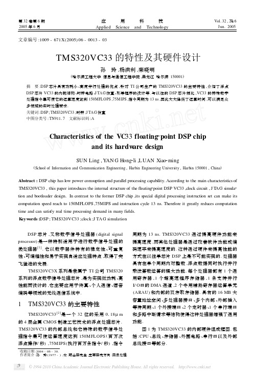
文章编号:1009-671X (2005)06-0013-03TMS320VC33的特性及其硬件设计孙 玲,杨洪利,栾晓明(哈尔滨工程大学信息与通信工程学院,黑龙江哈尔滨150001)摘 要:DSP 芯片具有功耗小、高度并行处理的优点,针对TI 公司生产的TMS320VC33的主要特性,介绍了浮点DSP 芯片VC33的内部结构、时钟电路、J TA G 仿真、引导程序的设计等.与以往的DSP 芯片相比,VC33的特殊数字处理指令集可使它的运算速度达到150MFLOPS ,75MIPS ,指令周期为13ns ,因此大大降低了运算时间,可以满足众多领域的实时处理要求.关键词:DSP ;TMS320VC33;时钟;J TA G 仿真中图分类号:TN91117 文献标识码:A收稿日期:2004-06-30.作者简介:孙 玲(1977-),女,硕士研究生,主要研究方向:图像处理.Characteristics of the VC 33floating 2point DSP chipand its hardw are designSUN Ling ,YAN G Hong 2li ,L UAN Xiao 2ming(School of Information and Communication Engineering ,Harbin Engineering University ,Harbin 150001,China )Abstract :DSP chip has low power comsuption and parallel processing capability.According to the main characteristics of TMS320VC33,this paper introduces the internal structure of the floating 2point DSP VC33,clock circuit ,J T AG simula 2tion and bootloader design.In contrast to the former DSP chip ,its special digital processing instruction set can make its computation speed reach to 150MFLOPS ,75MIPS and instruction cycle 13ns.Therefore it greatly reduces computation time and can satis fy real time processing demand in many fields.K eyw ords :DSP ;TMS320VC33;clock ;J TA G simulation DSP 芯片,又称数字信号处理器(digital signal processor )是一种特别适用于进行数字信号处理的微处理器[1].它以数字器件特有的稳定性、可重复性、可编程性和易于实现自适应处理特点,取得了突飞猛进的发展.TMS320VC3X 系列是隶属于TI 公司TMS320系列的浮点数字信号处理芯片,是为实现低功耗、高性能而设计的,它主要应用于传真、个人通信、语音编码等领域的无线通信系统中.1 TMS320VC33的主要特性TMS320VC33[2]是一个32位的采用0118μm的4层金属CMOS 制造工艺技术的浮点处理芯片.TMS320VC33的内部总线和它特殊的数字信号处理指令集可使运算速度达到150MFLOPS (百万次浮点操作/秒),75M IPS (执行百万条指令/秒),指令周期为13ns.TMS320VC33通过提高硬件功能来提高速度,而其他处理器是通过改善软件功能或编码速率来提高速度的.这种通过硬件来提高性能的方式在以往单芯片DSP 上是不可能实现的.处理器具有在单个周期内对整数,浮点数据同时执行并行乘法算数运算的强大功能.每个处理器都有1个通用寄存器,1个超高速程序存储器,1条支持并行I/O 口的DMA 通道,2个专用辅助寄存器运算单元(ARAU )和内部的双存取存储器.具有的16MB 大容量地址空间、多处理器接口、多个内部、外部插入等待周期、1个外接端口、2个定时器、1个串行端口和多路中断请求等结构使得这种处理器增强了通用功能.图1为TMS320VC33的内部硬件组成框图.包括:CPU 、总线、存储器、外围电路、串行口以及外部总线接口等部分. 第32卷第6期 应 用 科 技 Vol.32,№.62005年6月 Applied Science and Technology J un.2005图1 内部框图111 CPU的性能1)32位高性能的CPU;2)40位的算数逻辑运算单元(AL U),包括1个32位的桶形移位寄存器;3)2个地址生成器,包括8个辅助寄存器和2个辅助寄存器算数运算单元(ARAU);4)单指令周期可并行进行算数逻辑和乘法运算;5)两种低功耗方式;6)内核电压118V,I/O端口电压为313V; 112 总线的特点1)3条数据总线(PDA TA Bus,DDA TA Bus, DMADA TA Bus)将内部各个单元连接在一起;2)4条地址总线(PADDR Bus,DADDR1Bus, DADDR2Bus,DMAADDR Bus)传送执行指令所需的地址.113 存储器的容量片内34K×32bit的双存取SRAM,省去了外扩RAM带来的程序运行速度下降等问题.114 在片外围电路在片外围电路由以下几部分组成:1)用来周期产生中断的2个定时器;2)1个串行端口;3)1个直接存储器存取通道(DMA),用来协调并行I/O端口和CPU之间的操作;4)LQFP封装,144个引脚;5)增加了预解码选择引脚PA GE0~PA GE3,其寻址空间分别为0x000000~0x3FFFFF,0x400000~0x700000,0x800000~0xbFFFFF,0xc00000~0xFFFFFF.2 时钟电路时钟发生器为VC33提供时钟源,它包括1个内部的振荡器和1个锁相环电路(PLL).PLL在硬件上用户设置,最高可以进行5倍频.设计者可以自己选择时钟源:1)在XOU T和XIN引脚接入1个晶振,EXTCL K接地;2)把1个外部的时钟源直接接到EXTCL K引脚,XIN接地,XOU T悬空. TMS320VC33的CPU时钟有4种操作模式,这些模式可以控制时钟的分频比,具体的操作是通过外部的CL KMD0和CL KMD1引脚的设置来完成的. VC33的振荡方式如图2所示.图2 振荡电路・41・应 用 科 技 第32卷3 J TA G 仿真接口VC33含有1个专用仿真口来支持由IEEE 114911标准规范的J TA G 仿真,该端口由仿真器直接访问[3].提供基于扫描的仿真功能,这种设计大大方便了VC33软件的调试.为能与仿真器通信,用户设计的目标板上应有J TA G 仿真头.14脚的J TA G 仿真头信号及引脚位置如图3所示.图3 J TA G 仿真头当仿真头和J TA G 目标芯片之间的距离超过15cm 时,仿真信号要加缓冲器;小于15cm 时,不必加缓冲.图4是不加缓冲器的例子,其中的EMU0和EMU1信号必须通过上拉电阻连接到电源上,提供小于10μs 的信号上升时间,R 1和R 2可以取418Ω.图4 仿真信号的连接此外,也可以多处理器同时仿真.J TA G 仿真大大方便了汇编语言程序的调试,它可实时的访问目标板上CPU 的存储器,寄存器以及I/O 口等.调试软件的同时也可以调试硬件,给系统设计带来了很大的方便和灵活性.4 Bootloader 设计引导端接口如图5所示.图5 引导端接口 VC33硬件复位后,采样MCBL/MP 引脚如果为高电平,则片内ROM 映射到地址空间的0x000000~0x000FFF.因此,当复位时,由片内ROM 的0x809FC1地址处开始执行,此处放有一跳转指令以启动引导程序.在引导程序启动之前,一切外部活动都被禁止.引导程序需要1个小的堆栈区来存放调用和返回指令,SRAM 为它分配的空间的起始地址为0x809800.在引导程序结束之后,外部的逻辑或I/O 口线都可以安全地使MCBL 信号变为无效.然而,为了确保正确的操作,在引导程序没有完全结束前,CPU 不能执行任何代码和使用内部数据.图5的XFO 三态引脚能在复位时通过上拉电阻把DSP 置成MCBL 模式.代码段可以在应用程序开始时,使XFO 引脚逻辑低电平输出,把DSP 置成MP 模式:LDI 8000h ,STRPTS 4LDI2h ,IOF5 结束语TMS320VC33是TI 的3X 系列推出比较晚的一款,其性能可以理解为C31的改进型.设计者可以有1MB 的片内SRAM ,最大吞吐量能达到150MFLOPS.参考文献:[1]赵明忠,顾 斌.DSP 应用技术[M ].西安:西安电子科技大学出版社,2004.[2]李 刚.数字信号微处理器的原理及其开发应用[M ].天津:天津大学出版社,2000.[3]戴明桢,周建江.TMS320C54x DSP 结构,原理及应用[M ].北京:北京航空航天大学出版社,2001.[责任编辑:姜海丽]・51・第6期 孙 玲,等:TMS320VC33的特性及其硬件设计。
凯盛EBZ200掘进机电气使用说明书(2009年3月第1版)
KSZG/ZJ0220安装、使用产品前,请阅读本使用说明书 EBZ200型掘进机电气使用说明书执行标准:MT/T238.3-2006 Q/KSZS02.82—2008CNBM 凯盛重工有限公司恒通牌EBZ200型掘进机 电气使用说明书1凯盛重工有限公司(原淮南煤矿机械厂)1. 概述EBZ200型掘进机电气系统主要由矿用隔爆型电气控制箱(以下简称电控箱)、矿用隔爆型操作箱(以下简称操作箱)、隔爆型照明灯、隔爆型蜂鸣器、隔爆型急停按钮、甲烷断电仪等组成,在交流50Hz,1140v 的供电线路中,对掘进机的各种作业进行控制,并对各电动机和控制回路进行监测和保护,运行状态及故障中文显示。
使用条件:a)海拔高度不超过2000米; b)周围介质温度不超过-5℃~40℃; c)周围空气相对湿度不大于95%(25℃);d)在无强烈颠簸振动和冲击的环境中;e)在无破坏绝缘及腐蚀金属的气体和蒸汽的环境中 f)在能防雨雪与滴水的地方;g)在与水平面的安装倾斜不超过20°的环境中; h)电控设备的工作制为间断长期工作制; i)在具有甲烷爆炸性危险的煤矿井下。
2. 型号及结构特征 2.1 电控箱电控箱型号:KXJ-320/1140(660)E防爆形式: Exd[ib]I (隔爆兼本质安全型)电气使用说明书 恒通牌EBZ200型掘进机2 CNBM 凯盛重工有限公司电控箱有两大腔,左侧是接线腔,右侧是主腔,主腔门为快开门式,腔门由安装于箱体上下两端的悬臂支撑。
门与箱体之间用14个扣钉紧扣以实现隔爆结合,调节扣钉可以改变隔爆结合面的间隙,门与箱体之间有可靠的机械联锁,只有按下箱体左上方可自锁的紧急停止按钮,才能分合隔离开关,以保证隔离开关不带负荷操作。
隔离开关处于分断位置时才能拧紧闭锁螺杆,打开腔门,以保证腔门打开时,腔内所有元器件(但不包括隔离开关的电源侧)不带电,同时,闭锁螺杆拧出后,由于联锁,使隔离开关不能闭合。
mcp73833 73834中文手册

0.10
58 47 25
100 1000
3000 300 300
100
3.7 3.6 —
4.232 4.382 4.433 4.533 0.30
0.30
— — —
110 1100
最大输出电流限制
IMAX
—
1200
—
µA 充电中
µA 充电结束
µA 待机 (没有接电池或 PROG 悬空)
MCP73833/4
独立线性锂离子 / 锂聚合物电池 充电管理控制器
特点
• 完整的线性充电管理控制器 - 内部集成了功率晶体管 - 内部集成了电流检测 - 内部集成了反向阻断保护
• 可进行热调节的恒流 / 恒压控制 • 高精度预置稳压:
- 4.2V, 4.35V, 4.4V 或 4.5V, +0.75% • 可编程充电电流:最大 1A • 对深度放电的电池进行预充
电流 + 限制 -
111 kΩ
+ - 预充
+ - 终止 + - 充电
+ CA 10 kΩ
470.6 kΩ 48 kΩ
+ VA -
充电控制 定时器 状态逻辑
VBAT
STAT1 STAT2 PG (TE)
DS22005A_CN 第 2 页
2007 Microchip Technology Inc.
MCP73833/4
晶体管导通电阻 导通电阻
VPTH / VREG VPHYS
ITERM / IREG
VRTH / VREG RDSON
— 64 69 —
3.75 5.6 7.5 15
Microchip电子产品说明书

TREE 3: POWER MANAGEMENT 2Supervisors & Voltage Detectors Unique Strengths (So What)Broad Portfolio(It's likely we have your part)Small Packages: SOT-23 and SC-70 (Saves space)Industrial Standard Crosses (Replace high priced and poor delivery suppliers)Battery Management Unique Strengths (So What)Wide variety of charging solutions for Li-Ion batteries(We have the solution for you)Small SOT-23, MSOP, DFN and QFN packages (Saves space)DC-DC Converter (So What)Low-voltage operation (Saves Power)PFM/PWM Auto switch mode (PFM at low loads reduces current, saves power)Small SOT-23 packaging (Saves space)Step-down, Step-up (Efficiently increase or decrease voltage) Charge Pumps (So What)Low-voltage operation (Battery operation)Small SOT-23 packaging (Saves space)Step-down, Step-up (Efficiently increase or decrease voltage)Doubling & Inverting (Meets V OUT needs) Low-Frequency capable (Reduces EMI)Low-Current Operation (Saves power)LDO Unique Strengths (So What)Hundreds of voltages, currents, packages (We have a match for the need)0.5% V OUT accuracy (Fills precision need)Up to 1.5A output current(Able to power high load applications)Op Amp Unique Strengths (So What)Low current versus GBWP (Saves power)TC and MCP6XXX devices RR-I/O (Expands usable voltage range)MCP604X 1.4V operation(Two alkaline cells 90% used =1.8V)MCP644X, 450 nA operation (Use the batteries even longer)Comparators Unique Strengths (So What)Low current versus propagation delay (Saves power)Integrated Features (Saves space)1.8V and 1.4V operation (That stuff about the batteries)Programmable Gain Amplifier Unique Strengths (So What)MUX inputWide bandwidth (2 to 12 MHz) (Reduces demand on MCU I/O)System control of gain(Changes easier through software configurable hardware)TREE 5: LINEARTemperature Sensor Unique Strengths (So What)Wide variety of solutions: logic, voltage and digital output products(Multiple sensor needs met)Small packages (Saves space)Low operating current(Saves power, smaller supply)Field or factory programmable (Low cost vs. flexibility)Programmable hysteresis (Stop system cycling)Multi-drop capability (Great for large systems)Beta compensation (Compatible with processor substrate diodes)Resistance error correction (Compensates for measurement error from long PCB traces)Fan Controllers Unique Strengths (So What)Closed loop fan control (Adjust to meet target speed even on aging fans)Integrated temperature sensing (Consolidate thermal management)Multiple temperature measurements drive one fan (Consolidate thermal management)Built-in ramp rate control and spin up alogorithm (Quick time to market, lower acoustic noise)Ability to detect/predict failure of less expensive 2-wire fans (Saves system cost)Unique solutions for extending fan life and reducing acoustic noise(Less power, nuisance and long fan life)TREE 6: MIXED-SIGNALADC Unique Strengths (So What)Low current at max sampling rate (Saves power, system cost)Small SOT-23 and MSOP packages (Saves space)Up to 24-bit resolution(Ideal for precision sensitive designs)Differential & single ended inputs (Able to cover various design needs)Up to 6 ADC per device(Save board space, system cost)DAC Unique Strengths (So What)Low Supply Current (Saves power)Low DNL & INL (Better accuracy)Extended Temperature Range(Suitable for wide temperature applications)Digital Potentiometers Unique Strengths (So What)64/256 tap (6-bit to 8-bit resolution)(Sufficient resolution for most applications)Non-volatile Memory(Remembers last wiper setting on power up)WiperLock™ Technology(Locks NV memory setting-better than OTP)Small SOT-23 and 2 × 3 DFN packages (Saves space)Low CostMOSFET Drivers (So What)4.5V up to 30V Supply voltages (Fills many application needs)Up to 12A Peak output current(Able to meet demanding design needs)Outstanding robustness and latch-upi mmunity (Ours work when the others burn up)Low-FOM MOSFETs(Support high-efficency applications)TREE 4: POWER MANAGEMENT 3LIN Unique Strengths(So What)Compliant with LIN Bus Specs 1.3, 2.0, 2.1 andSAE J2602 (Allows for reliable interoperability)High EMI Low EME (Meets OEM requirements)On-board V REG available(Saves space, allows for MCU V CC flexibility)CAN Unique Strengths(So What)Simple SPI CAN controller is an easy way toadd CAN Ports (Short design cycles)High speed transceiver meets ISO-11898 (Drop inreplacement for industry standard transceivers)Low-cost, easy-to-use development tools(Tools easy to buy/use, quick design)I/O Expanders Unique Strengths(So What)Configurable inputs (interrupt configuration flexibility)Interrupt on pin change, or change fromregister default (interrupt source flexibility)Can disable automatic address incrementingwhen accessing the device(allows continual access to the port)The 16-bit devices can operate in 8-bit or 16-bitmode (easy to interface to 8-bit or 16-bit MCUs)IrDA Unique Strengths (So What)IrDA protocol handler embedded on chip(Complex design issue solved)Low cost developer's kit available to assistInfrared design-in (Quick design cycle)Small, cost-effective way of replacing serial links(No more wires)Enables system to wirelessly communicatewith PDA (Wireless connectivity solution) TREE 8: INTERFACEAnalog & InterfaceQuestion TreesAnalog & Interface Development ToolsDemonstration Boards, Evaluation Kits and AccessoriesAnalog & Interface LiteratureADM00313EV: MCP73830L 2 × 2 TDFN Evaluation BoardADM00352: MCP16301 High Voltage Buck Converter 600 mA Demonstration BoardADM00360: MCP16301 High Voltage Buck Coverter 300 mA D2PAK Demonstration BoardADM00427: MCP16323 Evaluation Board (Supports MCP16321 and MCP16322)ARD00386: MCP1640 12V/50 mA Two Cells Input Boost Converter Reference DesignMCP1252DM-BKLT: MCP1252 Charge Pump Backlight Demonstration BoardMCP1256/7/8/9EV: MCP1256/7/8/9 Charge Pump Evaluation BoardMCP1630RD-LIC1: MCP1630 Li-Ion Multi-Bay Battery Charger Reference DesignMCP1630DM-NMC1: MCP1630 NiMH Battery Charger Demonstration BoardMCP1640EV-SBC: MCP1640 Sync Boost Converter Evaluation BoardMCP1640RD-4ABC: MCP1640 Single Quad-A Battery Boost Converter Reference DesignMCP1650DM-LED1: MCP165X 3W White LED Demonstration BoardMCP1726EV: MCP1726 LDO Evaluation BoardMCP73831EV: MCP73831 Evaluation KitMCP7383XEV: MCP73837/8 AC/USB Dual Input Battery Charger Evaluation BoardMCP7383XRD-PPM: MCP7383X Li-Ion System Power Path Management Reference DesignMCP7384XEV: MCP7384X Li-Ion Battery Chager Evaluation BoardMCP73871EV: MCP73871 Load Sharing Li-Ion Battery Charger Evaluation BoardTC1016/17EV: TC1016/17 LDO Evaluation BoardVSUPEV: SOT-23-3 Voltage Supervisor Evaluation BoardPowerManagementThermalManagementMCP9700DM-PCTL: MCP9700 Thermal Sensor PICtail Demonstration BoardMCP9800DM-PCTL: MCP9800 Thermal Sensor PICtail Demonstration BoardTC72DM-PICTL: TC72 Digital Temperature Sensor PICtail Demonstration BoardTC74DEMO: TC74 Serial Daughter Thermal Sensor Demonstration BoardTC1047ADM-PCTL: TC1047A Temperature-to-Voltage Converter PICtail™ Demonstration BoardSerial GPIODM-KPLCD: GPIO Expander Keypad and LCD Demonstration BoardMCP23X17: MCP23X17 16-bit GPIO Expander Evaluation BoardInterface MCP2515DM-BM: MCP2515 CAN Bus Monitor Demonstration BoardMCP2515DM-PTPLS: MCP2515 PICtail™ Plus Daughter BoardMCP2515DM-PCTL: MCP2515 CAN Controller PICtail Demonstration BoardMCP215XDM: MCP215X/40 Data Logger Demonstration BoardMCP2140DM-TMPSNS: MCP2140 IrDA® Wireless Temp Demonstration BoardLinear ADM00375: MCP6H04 Evaluation BoardARD00354: MCP6N11 Wheatstone Bridge Reference DesignMCP651EV-VOS: MCP651 Input Offset Evaluation BoardMCP661DM-LD: MCP661 Line Driver Demo BoardMCP6S22DM-PCTL: MCP6S22 PGA PICtail Demonstration BoardMCP6S2XEV: MCP6S2X PGA Evaluation BoardMCP6SX2DM-PCTLPD: MCP6SX2 PGA Photodiode PICtail Demonstration BoardMCP6SX2DM-PCTLTH: MCP6SX2-PGA Thermistor PICtail Demonstration BoardMCP6V01RD-TCPL: MCP6V01 Thermocouple Auto-Zero Ref DesignMCP6XXXDM-FLTR: Active Filter Demo BoardPIC16F690DM-PCTLHS: Humidity Sensor PICtail Demonstration BoardMixed-Signal MCP3221 DM-PCTL: MCP3221 12-bit A/D PICtail Demonstration BoardMCP3421DM-BFG: MCP3421 Battery Fuel Gauge Demonstration BoardMCP3551DM-PCTL: MCP3551 PICtail Demonstration BoardMCP355XDM-TAS: MCP355X Tiny Application Sensor Demonstration BoardMCP355XDV-MS1: MCP3551 Sensor Demonstration BoardMCP402XEV: MCP402X Digital Potentiometer Evaluation BoardMCP4725EV: MCP4725, 12-bit Non-Volatile DAC Evaluation Board (Preferred One)MCP4725DM-PTPLS: MCP4725, 12-bit Non-Volatile DAC PICtail Demonstration BoardADM00398: MCP3911 ADC Evaluation Board for 16-bit MicrocontrollersCorporate Microchip Product Line Card - DS00890Brochures Analog and Interface Product Selector Guide - DS21060Low Cost Development Tools Solutions Guide - DS51560Analog and Interface Guide (Volume 1) - DS00924Analog and Interface Guide (Volume 2) - DS21975Cards Analog Highlights Card - DS21972Microchip Op Amp Discovery Card - DS21947Analog & Interface Question Trees - DS21728Mirochip SAR and Delta-Sigma ACD Discovery Card - DS22101Software Tools MAPS - Microchip Advanced Product SelectorAnalog & Interface Treelink Products PresentationDesign Guides Analog-to-Digital Converter Design Guide - DS21841Digital Potentiometers Design Guide - DS22017Programmable Gain Amplifiers (PGAs), Operational Amplifiersand Comparators Design Guide - DS21861Interface Products Design Guide - DS21883Signal Chain Design Guide - DS21825Power Solutions Design Guide - DS21913Temperature Sensor Design Guide - DS21895Voltage Supervisors Design Guide - DS51548DS21728JPowerManagementLDO & SwitchingRegulatorsCharge PumpDC/DC ConvertersPower MOSFETDriversPWM ControllersSystem SupervisorsVoltage DetectorsVoltage ReferencesLi-Ion/Li-PolymerBattery ChargersUSB Port PowerControllersMixed-SignalA/D ConverterFamiliesDigitalPotentiometersD/A ConvertersV/F and F/VConvertersEnergyMeasurement ICsCurrent/DC PowerMeasurement ICsInterfaceCAN PeripheralsInfraredPeripheralsLIN TransceiversSerial PeripheralsEthernet ControllersUSB PeripheralLinearOp AmpsInstrumentationAmpsProgrammableGain AmplifiersComparatorsSafety & SecurityPhotoelectricSmoke DetectorsIonization SmokeDetectorsIonization SmokeDetector Front EndsPiezoelectricHorn DriversThermalManagementTemperatureSensorsFan Control& HarwareManagementMotor DriveStepper and DC3Ф BrushlessDC Motor DriverTREE 7: MOTOR DRIVE Stepper Unique Strenghts(So What)Industrial standard footprint(Footprint compatible to industrial leaders)Perfect PIC® MCU companion chip(Solid field support)Micro-stepping ready(Enhanced performance)Integration protections(Simplify software development)3-Phase BLDC Unique Strengths(So What)Full-wave sinusoidal(Quiet operation, low mechanical vibration)Sensorless operation (Minimum externalcomponents, no software required)Thin form factor(Fits space concerned applications)Information subject to change. The Microchip name and logo, the Microchip logo, dsPIC, PIC are registered trademarks and MiWi, PICtail and ZENA are trademarks ofMicrochip Technology Incorporated in the U.S.A. and other countries. All other trademarks mentioned herein are property of their respective companies.© 2012, Microchip Technology Incorporated. All Rights Reserved.。
1uA超低功耗低压差稳压器-超低功耗LDO

○应用 ■ 手持式电池供电设备、微能量供电装置。 ■ 低功耗无线采集器装置、物联网无线装置、气体及电力监控装置、水热气表。 ■ 手持式医疗仪器仪表、手持抄表装置。 ■ 特适用于 MSP430、STM8L、STM32L、EFM32 等低功耗单片机系统的电源应用。 ■ 应用领域: 电力、地质、水利、海洋、气象、工控、农业、环境监测自动化等。
最小压差
0V 0V 10mV 50mV 0.1V 0.1V
最高可用电压 12 12 12
12 12 10.8
30
3.22 3.23 3.27 3.27 3.27 3.27 3.27 3.27 3.27 3.27 3.27 3.27 3.27 3.27 3.27
0.1V 8.3
40
60 100 160
A
供应电流
Iss
Vin=Vout+1V
1.0 2.9 uA 2
差压 Vout>2.5
Vd
Iout=160mA(注 2)
400 700 mV 1
注 1:负载和性线调整的测量是在固定结温下由低周期脉冲测试的。
注 2:低压差的测试是以输出电压下降到标称电压的 2%时测得。
○结构图
微控网
1/6
MCP33
≤1uA 超低功耗低压差稳压器
○真实最大范围
参数
符号
最大值
单位
输入电压
Vin
12
V
输出电流
Iout
500
mA
输出电压
Vout
Vss-0.3~Vin+0.3
V
连续总功耗
Pd
150
mW
工作环境温度
Topr
-30~+80
- 1、下载文档前请自行甄别文档内容的完整性,平台不提供额外的编辑、内容补充、找答案等附加服务。
- 2、"仅部分预览"的文档,不可在线预览部分如存在完整性等问题,可反馈申请退款(可完整预览的文档不适用该条件!)。
- 3、如文档侵犯您的权益,请联系客服反馈,我们会尽快为您处理(人工客服工作时间:9:00-18:30)。
1/6
MCP33
3.3V/≤1uA 超低功耗超低压差稳压器
○真实最大范围 参数
输入电压 输出电流 输出电压 连续总功耗 工作环境温度 贮藏温度 峰值回流焊温度
符号 Vin Iout Vout Pd Topr Tstg
最大值 12 500
Vss-0.3~Vin+0.3 150
-30~+80 -40~+125
MCP33
3.3V/≤1uA 超低功耗超低压差稳压器
○引脚定义
符号
功能描述
GND 接地端
Vin 电压输入端
Vout 电压输出端
○产品包装 器件型号 MCP33
封装 SOT-23
卷盘尺寸 直径 7 寸
带子宽度 8mm
数量 3000
产品中文全称: 3.3V 超低静态电流超低压差稳压器
○体积规格
备注 符合 RoHS 环保
○功能描述 MCP33 是一个高性能的三端引脚稳压器。透过激光制程技术使得输出电压十分准确和高精 度保证。应用了精良的 CMOS 工艺,将静态耗电量低至 1uA 或更低,达到了业界顶级水平。 适合应用于电池供电的设备以及极低待机电量消耗的需求场合。
○应用 ■ 电池供电设备、低功耗采集器装置。 ■ 掌上型电脑设备、手持仪器仪表。 ■ 便携式摄像机、录影机。 ■ 参考电压源。 ■ MSP430 控制器低功耗系统的电源应用。
3.31
3.28 3.28
3.35
3.28 3.28
3.4
3.28 3.28
3.47
3.28 3.28
3.5
3.28 3.28
3.6
3.28 3.28
3.63
3.28 3.28
3.7
பைடு நூலகம்
3.28 3.28
3.8
3.28 3.28
4
3.28 3.28
5
3.28 3.28
6
3.28 3.28
7
3.28 3.28
电路 1
电路 2
微控网
4/6
MCP33
3.3V/≤1uA 超低功耗超低压差稳压器
○ 应用测评参考
负载电流(mA)
空载 5
输入电压(V)
2
2 1.98
3
3 2.98
3.27
3.27 3.25
3.28
3.28 3.26
3.29
3.28 3.27
3.3
3.28 3.28
10mV 50mV 0.1V 0.1V
12
12 12 10.8
30
3.22 3.23 3.27 3.27 3.27 3.27 3.27 3.27 3.27 3.27 3.27 3.27 3.27 3.27 3.27
0.1V 8.3
40
60 100 160
3.26 3.27 3.2 3.27 3.27 3.23 3.09 3.27 3.27 3.27 3.12 3.27 3.27 3.27 3.22 3.27 3.27 3.27 3.26 3.27 3.27 3.27 3.26 3.27 3.27 3.27 3.26 3.27 3.27 3.27 3.26 3.27 3.27 3.27 3.27
○采购信息 采购详情请立即上微控网查阅 /
○手册更新 日期:2010.6.24.
微控网
6/6
MCP33
3.3V/≤1uA 超低功耗超低压差稳压器
○特性 ■ 最大输出电流 160mA (不超过封装最大可承受功率损耗) ■ 输出电压: 3.3V ■ 高准确度:输出电压 ±2% ■ 极低静态功耗: ≤1.0uA@VOUT=3.3V
■ 输入稳定性:典型值 0.2%/V
■ 低压差需求: 0.4V/160mA (VOUT=3.3V) ■ 超迷你封装: SOT23 (150mW 损耗可承受)
260
单位 V mA V
mW ℃ ℃ ℃
○电气特征(Ta=25℃,Vin-Vout+1V, 除非另有说明)
参数 输出电压
符号 Vout
条件 Iout=40mA,Vin=Vou t+1V
最小 -2.0
典型
最大 +2.0
单位 %
电路
性线控制
Iout=40mA,Vout+1V ≤Vin≤10.0V(注 1)
0.1V 0.17V 0.2V 0.37V
7
5.8 4.8 4.2
由上表可见,MCP33 最适合于单锂离子/锂聚合物可充电池的场合,此时压差最小,效率最 高,可输出电流也最大。测试过程中 MCP33 在可用电压和负载时 IQ 可维持在~0.5uA。
微控网
5/6
0.2 0.3 %/V 1
负载控制
Vin=Vout+1V,1mA≤ Iout≤80mA(注 1)
%/m 0.02 0.03
A
供应电流
Iss
Vin=Vout+1V
1.0 2.9 uA 2
差压 Vout>2.5
Vd
Iout=160mA(注 2)
400 700 mV 1
注 1:负载和性线调整的测量是在固定结温下由低周期脉冲测试的。
○典型应用电路
MCP33 应用电路非常简单易用。只需在输入和输出端并联一个 1uF 电容就可使用。由于采用 SOT-23 封装和使用外围元件少的特点,使得占用 PCB 面积和物理空间极小。这使用户可 减少产品的生产成本。再加上极小静态电流性能和低价格的优势;是低功耗设计中的首选电 源方案。
微控网
注 2:低压差的测试是以输出电压下降到标称电压的 2%时测得。
○结构图
微控网
2/6
MCP33
3.3V/≤1uA 超低功耗超低压差稳压器
○典型工作特性
微控网
3/6
MCP33
3.3V/≤1uA 超低功耗超低压差稳压器
○测试电路
8
3.28 3.28
9
3.28 3.28
10
3.28 3.28
11
3.28 3.28
12
3.28 3.28
最小压差 0V 0V
最高可用电压 12 12
10
15 17.2 20
3.26 3.27 3.28 3.27 3.28 3.28 3.27 3.27 3.28 3.28 3.28 3.28 3.28 3.28 3.28 3.28 3.28 3.28 3.28 3.28 3.28 3.28 3.28 3.28 3.28 3.28 3.28 3.28 3.28 3.28 3.28 3.28 3.28 3.28 3.28 3.28 3.28 3.28 3.28 3.28 3.28 3.28 3.28 3.28 3.28 3.28 3.28 3.28 3.28 3.28 3.28 3.28 3.28 3.28 3.28 3.28 3.28 3.28 3.28 3.28 3.28 3.28 3.28 3.28 3.28 3.28 3.28 3.28 3.28 3.28
