mic5206
MCW0406MD4991BP100;MCW0406MD2490BP100;MCW0406MD4990BP100;中文规格书,Datasheet资料
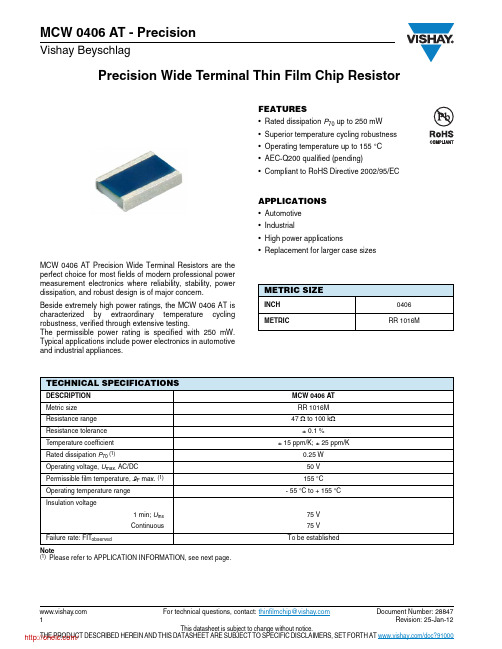
SOLDER PAD DIMENSIONS
G Y Z X
RECOMMENDED SOLDER PAD DIMENSIONS
REFLOW SOLDERING TYPE MCW 0406 AT G (mm) 0.35 Y (mm) 0.55 X (mm) 1.75 Z (mm) 1.45
Note • The rated dissipation applies only if the permitted film temperature is not exceeded. Furthermore, a high level of ambient temperature or of power dissipation may raise the temperature of the solder joint, hence special solder alloys or boardmaterials may be required to maintain the reliability of the assembly. Specified power rating above 125 °C requires dedicated heat-sink pads, which depend on boardmaterials. The given solder pad dimensions reflect the considerations for board design and assembly as outlined e.g. in standards IEC 61188-5-x, or in publication IPC-7351. They do not guarantee any supposed thermal properties, particularly as these are also strongly influenced by many other parameters. Still, the given solder pad dimensions will be found adequate for most general applications, e.g. those referring to “standard operation mode”. Please note however that applications for “power operation mode” or “advanced temperature mode” require special considerations for the design of solder pads and adjacent conductor areas.
BR8230 芯片数据手册 v1.02
I
BR6211 数据手册
版本历史
版本 V1.01 V1.02
日期
修改内容 章节 页码 初始版本 增加工作电流 内容
II
BR6211 数据手册
目录
版本历史................................................................................................................................................................... II 目录.......................................................................................................................................................................... III 附图目录................................................................................................................................................................... V 表格目录..................................................................................................................................................................VI 缩写与术语......
MIC2026-1BM中文资料

VEN
Enable Input Threshold
low-to-high transition high-to-low transition
Enable Input Hysteresis
IEN
Enable Input Current
Enable Input Capacitance
VEN = 0V to 5.5V
Load
Micrel, Inc. • 1849 Fortune Drive • San Jose, CA 95131 • USA • tel + 1 (408) 944-0800 • fax + 1 (408) 944-0970 •
March 2000
1
MIC2026/2076
The MIC2026/76 are internally current limited and have thermal shutdown that protects the device and load.
The MIC2076 offers “smart” thermal shutdown that reduces current consumption in fault modes. When a thermal shutdown fault occurs, the output is latched off until the faulty load is removed. Removing the load or toggling the enable input will reset the device output.
Electrical Characteristics
VIN = +5V; TA = 25°C, bold values indicate –40°C ≤ TA ≤ +85°C; unless noted
芯片标志对映的型号

(中国.厦门) China.Xiamen RF-Micom co.,Ltd Email:sales@ Telephone:0086-592-5713956 Fax:5201617Analog Marking InformationTeeny™, IttyBitty®, and TinyFET® Part IdentificationTeeny™ SC-70, IttyBitty®, TinyFET®, and other SOT-143, or SOT-23 packaged devices use abbreviated markings for identification because of their small size.Mark Part Number Description NoteA11MIC6211BM5IttyBitty® Op AmpA12LMC7101BIM5Low-Power Operational AmplifierA12A LMC7101AIM5[Improved Precision] Low-Power Op AmpA13MIC7111BM5 2.4V IttyBitty® Rail-to-Rail Input/Output Op AmpA14MIC7211BM5IttyBitty® Rail-to-Rail Input Comparator Push-pull outputA15MIC7221BM5IttyBitty® Rail-to-Rail Input Comparator Open-drain outputA16MIC7201BM5GainBlock™ Difference AmplifierA17MIC7300BM5High-Output Drive Rail-to-Rail Op AmpA21MIC910BM5135MHz Low-Power SOT-23-5 Op AmpA22MIC911BM5105MHz Low-Power SOT-23-5 Op AmpA23MIC912BM5200MHz Low-Power SOT-23-5 Op AmpA24MIC913BM5350MHz Low-Power SOT-23-5 Op AmpA26MIC914BM5160MHz Low-Power SOT-23-5 Op AmpA30MIC918BC551MHz Low-Power SOT-23-5/SC-70 Op AmpA31MIC919BC527MHz Low-Power SOT-23-5/SC-70 Op AmpA32MIC860BC5Teeny™ Ultra Low-Power Op AmpA33MIC861BC5Teeny™ Ultra Low-Power Op AmpA34MIC862BM8Dual Ultra Low-Power Op Amp SOT-23-8A35MIC863BM8Dual Ultra Low-Power Op Amp SOT-23-8A37MIC920BC580MHz Low-Power SC-70 Op AmpA38MIC921BC545MHz Low-Power SC-70 Op AmpA39MIC922BC5230MHz Low-Power SC-70 Op AmpA40MIC923BC5410MHz Low-Power SC-70 Op AmpA51MIC6251BM5IttyBitty® Instrumentation Amplifier+2, +1, –1 gain amp.A52MIC6252BM5IttyBitty® Instrumentation Amplifier+0.5, +1 gain amp.,avg. value amp.B10MIC6270BM5IttyBitty® ComparatorB11MIC833BM5Latched Comparator with ReferenceB12MIC834BM5Comparator with ReferenceB13MIC841HBC5Comparator with Reference in SC70-5B14MIC841LBC5Comparator with Reference in SC70-5B15MIC841NBC5Comparator with Reference in SC70-5B16MIC842HBC5Comparator with Reference in SC70-5B17MIC842LBC5Comparator with Reference in SC70-5B18MIC842NBC5Comparator with Reference in SC70-5C10MIC2660BM5IttyBitty® Charge PumpD10MIC4416BM4IttyBitty® Low-Side MOSFET Driver Non-invertingD11MIC4417BM4IttyBitty® Low-Side MOSFET Driver InvertingML10MIC4416BM4IttyBitty® Low-Side MOSFET DriverF10MIC2514BM5IttyBitty® Integrated High-Side SwitchH10MIC5018BM4IttyBitty® High-Side MOSFET Driver Non-invertingMH10MIC5018BM4IttyBitty® High-Side MOSFET DriverIJ ETC/MIC809JU Microprocessor Reset Circuit 4.00VIL ETC/MIC809LU…Microprocessor Reset Circuit 4.63VIM ETC/MIC809MU…Microprocessor Reset Circuit 4.38VIR ETC/MIC809RU…Microprocessor Reset Circuit 2.63VIS ETC/MIC809SU…Microprocessor Reset Circuit 2.93VIT ETC/MIC809TU…Microprocessor Reset Circuit 3.08VJJ ETC/MIC810JU…Microprocessor Reset CircuitJL ETC/MIC810LU…Microprocessor Reset Circuit 4.63VJM ETC/MIC810MU…Microprocessor Reset Circuit 4.38VJR ETC/MIC810RU…Microprocessor Reset Circuit 2.63VJS ETC/MIC810SU…Microprocessor Reset Circuit 2.93VJT ETC/MIC810TU…Microprocessor Reset Circuit 3.08VKJ ETC/MIC811JU Microprocessor Reset Circuit 4.00VKL ETC/MIC811LU…Microprocessor Reset Circuit 4.63VKM ETC/MIC811MU…Microprocessor Reset Circuit 4.38VKR ETC/MIC811RU…Microprocessor Reset Circuit 2.63VKS ETC/MIC811SU…Microprocessor Reset Circuit 2.93VK S MIC811SUY Microprocessor Reset CircuitKT ETC/MIC811TU…Microprocessor Reset Circuit 3.08VLAN MIC5213-1.8BC5Teeny™ SC-70 µCap LDO RegulatorLAM MIC5213-2.5BC5Teeny™ SC-70 µCap LDO RegulatorLAQ MIC5213-2.6BC5Teeny™ SC-70 µCap LDO RegulatorLAL MIC5213-2.7BC5Teeny™ SC-70 µCap LDO RegulatorLAJ MIC5213-2.8BC5Teeny™ SC-70 µCap LDO RegulatorLAG MIC5213-3.0BC5Teeny™ SC-70 µCap LDO RegulatorLAE MIC5213-3.3BC5Teeny™ SC-70 µCap LDO RegulatorLAD MIC5213-3.6BC5Teeny™ SC-70 µCap LDO RegulatorLAB MIC5213-5.0BC5Teeny™ SC-70 µCap LDO RegulatorJanuary 20042Micrel SemiconductorAnalog Marking InformationMark Part Number Description NoteLA28MIC5203-2.8BM480mA Low-Dropout Regulator (SOT-143)Fixed output (also see LK)LA30MIC5203-3.0BM480mA Low-Dropout Regulator (SOT-143)Fixed outputLA33MIC5203-3.3BM480mA Low-Dropout Regulator (SOT-143)Fixed outputLA36MIC5203-3.6BM480mA Low-Dropout Regulator (SOT-143)Fixed outputLA38MIC5203-3.8CM480mA Low-Dropout Regulator (SOT-143)Fixed outputLA40MIC5203-4.0BM480mA Low-Dropout Regulator (SOT-143)Fixed outputLA45MIC5203-4.5BM480mA Low-Dropout Regulator (SOT-143)Fixed outputLA47MIC5203-4.7BM480mA Low-Dropout Regulator (SOT-143)Fixed outputLA50MIC5203-5.0BM480mA Low-Dropout Regulator (SOT-143)Fixed outputLBAA MIC5205BM5150mA Low-Dropout Regulator Adjustable outputKBAA MIC5205YM5150mA Low-Dropout Regulator Fixed outputLB38MIC5205-3.8BM5150mA Low-Dropout Regulator Fixed outputLB40MIC5205-4.0BM5150mA Low-Dropout Regulator Fixed outputLB25MIC5205-2.5BM5150mA Low-Dropout Regulator Fixed outputKB25MIC5205-2.5YM5150mA Low-Dropout Regulator Fixed outputLB27MIC5205-2.7BM5150mA Low-Dropout Regulator Fixed outputLB2J MIC5205-2.85BM5150mA Low-Dropout Regulator Fixed outputLB28MIC5205-2.8BM5150mA Low-Dropout Regulator Fixed outputLB29MIC5205-2.9BM5150mA Low-Dropout Regulator Fixed outputLB30MIC5205-3.0BM5150mA Low-Dropout Regulator Fixed outputLB31MIC5205-3.1BM5150mA Low-Dropout Regulator Fixed outputLB32MIC5205-3.2BM5150mA Low-Dropout Regulator Fixed outputLB33MIC5205-3.3BM5150mA Low-Dropout Regulator Fixed outputLB36MIC5205-3.6BM5150mA Low-Dropout Regulator Fixed outputLB38MIC5205-3.8BM5150mA Low-Dropout Regulator Fixed outputLB40MIC5205-4.0BM5150mA Low-Dropout Regulator Fixed outputLB48MIC5205-4.8BM5150mA Low-Dropout Regulator Fixed outputLB50MIC5205-4.0BM5150mA Low-Dropout Regulator Fixed outputLDAA MIC5206BM5150mA Low-Noise LDO Regulator Adjustable outputLD25MIC5206-2.5BM5150mA Low-Noise LDO Regulator Fixed outputLD27MIC5206-2.7BM5150mA Low-Noise LDO Regulator Fixed outputLD2J MIC5206-2.85BM5150mA Low-Noise LDO Regulator Fixed outputLD29MIC5206-2.9BM5150mA Low-Noise LDO Regulator Fixed outputLD30MIC5206-3.0BM5150mA Low-Noise LDO Regulator Fixed outputLD32MIC5206-3.2BM5150mA Low-Noise LDO Regulator Fixed outputLD33MIC5206-3.3BM5150mA Low-Noise LDO Regulator Fixed outputLD34MIC5206-3.4BM5150mA Low-Noise LDO Regulator Fixed outputLD36MIC5206-3.6BM5150mA Low-Noise LDO Regulator Fixed outputLD38MIC5206-3.8BM5150mA Low-Noise LDO Regulator Fixed outputLD40MIC5206-4.0BM5150mA Low-Noise LDO Regulator Fixed outputLD41MIC5206-4.15BM5150mA Low-Noise LDO Regulator Fixed outputLD50MIC5206-5.0BM5150mA Low-Noise LDO Regulator Fixed outputLEAA MIC5207BM5180mA Low-Noise LDO Regulator Adjustable outputLE13MIC5207-1.3BM5180mA Low-Noise LDO Regulator Fixed outputLE18MIC5207-1.8BM5180mA Low-Noise LDO Regulator Fixed outputLE25MIC5207-2.5BM5180mA Low-Noise LDO Regulator Fixed outputLE28MIC5207-2.8BM5180mA Low-Noise LDO Regulator Fixed outputLE29MIC5207-2.9BM5180mA Low-Noise LDO Regulator Fixed outputLE30MIC5207-3.0BM5180mA Low-Noise LDO Regulator Fixed outputLE31MIC5207-3.1BM5180mA Low-Noise LDO Regulator Fixed outputLE32MIC5207-3.2BM5180mA Low-Noise LDO Regulator Fixed outputLE33MIC5207-3.3BM5180mA Low-Noise LDO Regulator Fixed outputLE36MIC5207-3.6BM5180mA Low-Noise LDO Regulator Fixed outputLE38MIC5207-3.8BM5180mA Low-Noise LDO Regulator Fixed outputLE40MIC5207-4.0BM5180mA Low-Noise LDO Regulator Fixed outputLE50MIC5207-5.0BM5180mA Low-Noise LDO Regulator Fixed outputNE18MIC5207-1.8BD5180mA Low-Noise LDO Regulator Fixed outputLFBB MIC5211-1.8BM6Dual 50mA LDO Voltage Regulator Fixed output, special codeLFCC MIC5211-2.5BM6Dual 50mA LDO Voltage Regulator Fixed outputLFDD MIC5211-2.7BM6Dual 50mA LDO Voltage Regulator Fixed outputLFEE MIC5211-2.8BM6Dual 50mA LDO Voltage Regulator Fixed outputLFGG MIC5211-3.0BM6Dual 50mA LDO Voltage Regulator Fixed outputLFLL MIC5211-3.3BM6Dual 50mA LDO Voltage Regulator Fixed outputLFQQ MIC5211-3.6BM6Dual 50mA LDO Voltage Regulator Fixed outputLFXX MIC5211-5.0BM5Dual 50mA LDO Voltage Regulator Fixed outputLFBC MIC5211-1.8/2.5BM6Dual 50mA LDO Voltage Regulator Fixed outputLFBL MIC5211-1.8/3.3BM6Dual 50mA LDO Voltage Regulator Fixed outputLFCL MIC5211-2.5/3.3BM6Dual 50mA LDO Voltage Regulator Fixed outputLFLX MIC5211-3.3/5.0BM6Dual 50mA LDO Voltage Regulator Fixed outputLGAA MIC5219BM5500mA-Peak Output LDO Regulator Adjustable outputLG25MIC5219-2.5BM5500mA-Peak Output LDO Regulator Fixed outputLG18MIC5219-1.8BM5500mA-Peak Output LDO Regulator Fixed outputLG30MIC5219-3.0BM5500mA-Peak Output LDO Regulator Fixed outputLG31MIC5219-3.0BM5500mA-Peak Output LDO Regulator Fixed outputLG33MIC5219-3.3BM5500mA-Peak Output LDO Regulator Fixed outputLG36MIC5219-3.6BM5500mA-Peak Output LDO Regulator Fixed outputLG50MIC5219-5.0BM5500mA-Peak Output LDO Regulator Fixed outputLG26MIC5219-2.6BM5500mA-Peak Output LDO Regulator Fixed outputLG27MIC5219-2.7BM5500mA-Peak Output LDO Regulator Fixed outputLG2J MIC5219-2.85BM5500mA-Peak Output LDO Regulator Fixed outputLG28MIC5219-2.8BM5500mA-Peak Output LDO Regulator Fixed outputLG29MIC5219-2.9BM5500mA-Peak Output LDO Regulator Fixed outputJanuary 20043Micrel SemiconductorAnalog Marking InformationMark Part Number Description NoteLHAA MIC5216BM5500mA-Peak Output LDO Regulator Adjustable outputLH25MIC5216-2.5BM5500mA-Peak Output LDO Regulator Fixed outputLH30MIC5216-3.0BM5500mA-Peak Output LDO Regulator Fixed outputLH33MIC5216-3.3BM5500mA-Peak Output LDO Regulator Fixed outputLH36MIC5216-3.6BM5500mA-Peak Output LDO Regulator Fixed outputLH38MIC5216-3.8BM5500mA-Peak Output LDO Regulator Fixed outputLH40MIC5216-4.0BM5500mA-Peak Output LDO Regulator Fixed outputLH50MIC5216-5.0BM5500mA-Peak Output LDO Regulator Fixed outputLK26MIC5203-2.6BM580mA Low-Dropout Regulator (SOT-23-5)Fixed output (also see LA)LK28MIC5203-2.8BM580mA Low-Dropout Regulator (SOT-23-5)Fixed outputLK30MIC5203-3.0BM580mA Low-Dropout Regulator (SOT-23-5)Fixed outputLK33MIC5203-3.3BM580mA Low-Dropout Regulator (SOT-23-5)Fixed outputLK36MIC5203-3.6BM580mA Low-Dropout Regulator (SOT-23-5)Fixed outputLK38MIC5203-3.8BM580mA Low-Dropout Regulator (SOT-23-5)Fixed outputLK40MIC5203-4.0BM580mA Low-Dropout Regulator (SOT-23-5)Fixed outputLK45MIC5203-4.5BM580mA Low-Dropout Regulator (SOT-23-5)Fixed outputLK47MIC5203-4.7BM580mA Low-Dropout Regulator (SOT-23-5)Fixed outputLK50MIC5203-5.0BM580mA Low-Dropout Regulator (SOT-23-5)Fixed outputLLAA MIC5270BM5IttyBitty® Negative Low-Dropout Regulator Adjustable outputLL30MIC5270-3.0BM5IttyBitty® Negative Low-Dropout Regulator Fixed outputLL41MIC5270-4.1BM5IttyBitty® Negative Low-Dropout Regulator Fixed outputLL50MIC5270-5.0BM5IttyBitty® Negative Low-Dropout Regulator Fixed outputLM2H MIC5231-2.75BM5Micropower µCap LDO Regulator Fixed outputLM30MIC5231-3.0BM5Micropower µCap LDO Regulator Fixed outputLM33MIC5231-3.3BM5Micropower µCap LDO Regulator Fixed outputLM50MIC5231-5.0BM5Micropower µCap LDO Regulator Fixed outputLN12MIC5258-1.2BM5150mA µCap CMOS LDO Regulator w/Power Good Fixed outputKN12MIC5258-1.2YM5150mA µCap CMOS LDO Regulator w/Power Good Fixed outputLS20MIC5245-2.0BM5150mA IttyBitty® CMS LDO Regulator Fixed outputLS21MIC5245-2.1BM5150mA IttyBitty® CMS LDO Regulator Fixed outputLS22MIC5245-2.2BM5150mA IttyBitty® CMS LDO Regulator Fixed outputLS23MIC5245-2.3BM5150mA IttyBitty® CMS LDO Regulator Fixed outputLS25MIC5245-2.5BM5150mA IttyBitty® CMS LDO Regulator Fixed outputLS26MIC5245-2.6BM5150mA IttyBitty® CMS LDO Regulator Fixed outputLS27MIC5245-2.7BM5150mA IttyBitty® CMS LDO Regulator Fixed outputLS28MIC5245-2.8BM5150mA IttyBitty® CMS LDO Regulator Fixed outputLS2J MIC5245-2.85BM5150mA IttyBitty® CMS LDO Regulator Fixed outputLS30MIC5245-3.0BM5150mA IttyBitty® CMS LDO Regulator Fixed outputLS31MIC5245-3.1BM5150mA IttyBitty® CMS LDO Regulator Fixed outputLS32MIC5245-3.2BM5150mA IttyBitty® CMS LDO Regulator Fixed outputLS33MIC5245-3.3BM5150mA IttyBitty® CMS LDO Regulator Fixed outputLS35MIC5245-3.5BM5150mA IttyBitty® CMS LDO Regulator Fixed outputLS50MIC5245-5.0BM5150mA IttyBitty® CMS LDO Regulator Fixed outputLT15MIC5246-1.5BM5150mA µCap CMOS LDO Regulator Fixed outputLT21MIC5246-2.1BM5150mA µCap CMOS LDO Regulator Fixed outputLT25MIC5246-2.5BM5150mA µCap CMOS LDO Regulator Fixed outputLT26MIC5246-2.6BM5150mA µCap CMOS LDO Regulator Fixed outputLT27MIC5246-2.7BM5150mA µCap CMOS LDO Regulator Fixed outputLT2J MIC5246-2.85BM5150mA µCap CMOS LDO Regulator Fixed outputLT28MIC5246-2.85BM5150mA µCap CMOS LDO Regulator Fixed outputLT30MIC5246-3.0BM5150mA µCap CMOS LDO Regulator Fixed outputLT31MIC5246-3.1BM5150mA µCap CMOS LDO Regulator Fixed outputLT33MIC5246-3.3BM5150mA µCap CMOS LDO Regulator Fixed outputLU15MIC5247-1.5BM5150mA Low-Voltage µCap Linear Regulator Fixed outputLU16MIC5247-1.6BM5150mA Low-Voltage µCap Linear Regulator Fixed outputLU1J MIC5247-1.85BM5150mA Low-Voltage µCap Linear Regulator Fixed outputLU18MIC5247-1.8BM5150mA Low-Voltage µCap Linear Regulator Fixed outputLU20MIC5247-2.0BM5150mA Low-Voltage µCap Linear Regulator Fixed outputLU21MIC5247-2.1BM5150mA Low-Voltage µCap Linear Regulator Fixed outputLU22MIC5247-2.2BM5150mA Low-Voltage µCap Linear Regulator Fixed outputLU24MIC5247-2.4BM5150mA Low-Voltage µCap Linear Regulator Fixed outputNU18MIC5247-1.8BD5150mA Low-Voltage µCap Linear Regulator Fixed outputNU20MIC5247-2.0BD5150mA Low-Voltage µCap Linear Regulator Fixed outputLV12MIC5248-1.2BM5150mA µCap CMOS LDO Regulator with Power Good Fixed outputKV12MIC5248-1.2YM5150mA µCap CMOS LDO Regulator with Power Good Fixed outputNW25MIC5255-2.5BD5150mA Low Noise µCap CMOS LDO Fixed outputLW25MIC5255-2.5BM5150mA Low Noise µCap CMOS LDO Fixed outputKW25MIC5255-2.5YM5150mA Low Noise µCap CMOS LDO Fixed outputNW26MIC5255-2.6BM5150mA Low Noise µCap CMOS LDO Fixed outputLW26MIC5255-2.6BM5150mA Low Noise µCap CMOS LDO Fixed outputLW2H MIC5255-2.75BM5150mA Low Noise µCap CMOS LDO Fixed outputNW27MIC5255-2.7BD5150mA Low Noise µCap CMOS LDO Fixed outputLW27MIC5255-2.7BM5150mA Low Noise µCap CMOS LDO Fixed outputNW2J MIC5255-2.85BD5150mA Low Noise µCap CMOS LDO Fixed outputLW2J MIC5255-2.85BM5150mA Low Noise µCap CMOS LDO Fixed outputNW28MIC5255-2.8BD5150mA Low Noise µCap CMOS LDO Fixed outputLW28MIC5255-2.8BM5150mA Low Noise µCap CMOS LDO Fixed outputNW29MIC5255-2.9BD5150mA Low Noise µCap CMOS LDO Fixed outputLW29MIC5255-2.9BM5150mA Low Noise µCap CMOS LDO Fixed outputJanuary 20044Micrel SemiconductorAnalog Marking InformationMark Part Number Description NoteNW30MIC5255-3.0BD5150mA Low Noise µCap CMOS LDO Fixed output LW30MIC5255-3.0BM5150mA Low Noise µCap CMOS LDO Fixed output LW31MIC5255-3.1BM5150mA Low Noise µCap CMOS LDO Fixed output LW32MIC5255-3.2BM5150mA Low Noise µCap CMOS LDO Fixed output NW33MIC5255-3.3BD5150mA Low Noise µCap CMOS LDO Fixed output LW33MIC5255-3.3BM5150mA Low Noise µCap CMOS LDO Fixed output LX26MIC5256-2.6BM5150mA µCap LDO with Error Flag Fixed output LX27MIC5256-2.7BM5150mA µCap LDO with Error Flag Fixed output LX28MIC5256-2.8BM5150mA µCap LDO with Error Flag Fixed output LX2J MIC5256-2.85BM5150mA µCap LDO with Error Flag Fixed output LX29MIC5256-2.9BM5150mA µCap LDO with Error Flag Fixed output LX30MIC5256-3.0BM5150mA µCap LDO with Error Flag Fixed output LX31MIC5256-3.1BM5150mA µCap LDO with Error Flag Fixed output LX33MIC5256-3.3BM5150mA µCap LDO with Error Flag Fixed output NX2J MIC5256-2.85BD5150mA µCap LDO with Error Flag Fixed output LZxx MIC5159-x.xBM6Programmable Current-Limit µCap LDO Regulator Controller Fixed output LZAA MIC5159-BM6Programmable Current-Limit µCap LDO Regulator Controller Adjustable output L2AA MIC5235-BM5Ultra-Low Quiescent Current, 150mA µCap LDO Regulator Adjustable output L215MIC5235-1.5BM5Ultra-Low Quiescent Current, 150mA µCap LDO Regulator Fixed output L218MIC5235-1.8BM5Ultra-Low Quiescent Current, 150mA µCap LDO Regulator Fixed output L225MIC5235-2.5BM5Ultra-Low Quiescent Current, 150mA µCap LDO Regulator Fixed output L227MIC5235-2.7BM5Ultra-Low Quiescent Current, 150mA µCap LDO Regulator Fixed output L230MIC5235-3.0BM5Ultra-Low Quiescent Current, 150mA µCap LDO Regulator Fixed output L233MIC5235-3.3BM5Ultra-Low Quiescent Current, 150mA µCap LDO Regulator Fixed output L250MIC5235-5.0BM5Ultra-Low Quiescent Current, 150mA µCap LDO Regulator Fixed outputL3AA MIC5233-BM5High Input Voltage, Low IQ µCap LDO Regulator Adjustable outputL318MIC5233-1.8BM5High Input Voltage, Low IQ µCap LDO Regulator Fixed outputL325MIC5233-2.5BM5High Input Voltage, Low IQ µCap LDO Regulator Fixed outputL318MIC5233-1.8BM5High Input Voltage, Low IQ µCap LDO Regulator Fixed outputL330MIC5233-3.0BM5High Input Voltage, Low IQ µCap LDO Regulator Fixed outputL333MIC5233-3.3BM5High Input Voltage, Low IQ µCap LDO Regulator Fixed outputL350MIC5233-5.0BM5High Input Voltage, Low IQµCap LDO Regulator Fixed output L409MIC5238-0.9BM5Ultra-Low Quiesent Current, 150mA µCap LDO RegulatorL410MIC5238-1.0BM5Ultra-Low Quiesent Current, 150mA µCap LDO RegulatorL411MIC5238-1.1BM5Ultra-Low Quiesent Current, 150mA µCap LDO RegulatorL411MIC5238-1.1YM5Ultra-Low Quiesent Current, 150mA µCap LDO RegulatorL412MIC5238-1.2BM5Ultra-Low Quiesent Current, 150mA µCap LDO RegulatorL413MIC5238-1.3BM5Ultra-Low Quiesent Current, 150mA µCap LDO RegulatorL413MIC5238-1.3YM5Ultra-Low Quiesent Current, 150mA µCap LDO RegulatorL5xx MIC5268150mA µCap CMOS LDO Regulator w/Power GoodL512MIC5268-1.2BM5150mA µCap CMOS LDO Regulator w/Power GoodL618MIC5252-1.8BM5150mA Low Noise µCap CMOS LDOL625MIC5252-2.5BM5150mA Low Noise µCap CMOS LDOL628MIC5252-2.8BM5150mA Low Noise µCap CMOS LDOL62J MIC5252-2.85BM5150mA Low Noise µCap CMOS LDOL630MIC5252-3.0BM5150mA Low Noise µCap CMOS LDOL64H MIC5252-4.75BM5150mA Low Noise µCap CMOS LDO618MIC5252-1.8BML150mA Low Noise µCap CMOS LDO625MIC5252-2.5BML150mA Low Noise µCap CMOS LDO62J MIC5252-2.85BML150mA Low Noise µCap CMOS LDO628MIC5252-2.8BML150mA Low Noise µCap CMOS LDO630MIC5252-3.0BML150mA Low Noise µCap CMOS LDO64H MIC5252-4.75BML150mA Low Noise µCap CMOS LDOL8xx MIC5305µCap 80mA Low-Dropout RegulatorN8xx MIC5305 (D5)µCap 80mA Low-Dropout RegulatorN815MIC5305-1.5BD5µCap 80mA Low-Dropout RegulatorN818MIC5305-1.8BD5µCap 80mA Low-Dropout RegulatorN82J MIC5305-2.85BD5µCap 80mA Low-Dropout RegulatorNAA MIC5305BD5µCap 80mA Low-Dropout Regulator Adjustable815MIC5305-1.5BMLµCap 80mA Low-Dropout Regulator818MIC5305-1.8BMLµCap 80mA Low-Dropout Regulator825MIC5305-2.5BMLµCap 80mA Low-Dropout Regulator826MIC5305-2.6BMLµCap 80mA Low-Dropout Regulator827MIC5305-2.7BMLµCap 80mA Low-Dropout Regulator828MIC5305-2.8BMLµCap 80mA Low-Dropout Regulator829MIC5305-2.9BMLµCap 80mA Low-Dropout Regulator830MIC5305-3.0BMLµCap 80mA Low-Dropout RegulatorLL ETC/MIC812LU…Microprocessor Reset Circuit 4.63VLM ETC/MIC812MU…Microprocessor Reset Circuit 4.38VLR ETC/MIC812RU…Microprocessor Reset Circuit 2.63VLS ETC/MIC812SU…Microprocessor Reset Circuit 2.93VLT ETC/MIC812TU…Microprocessor Reset Circuit 3.08VNA ETC/MIC1810-5U Microprocessor Reset Circuit 4.62VNB ETC/MIC1810-10U Microprocessor Reset Circuit 4.37VNC ETC/MIC1810-15U Microprocessor Reset Circuit 4.12VND ETC/MIC1815-10U Microprocessor Reset Circuit 2.88VNE ETC/MIC1815-20U Microprocessor Reset Circuit 2.55VNR ETC/MIC6315-26D3U Open-Drain µP Reset Circuit 2.63V, 140msJanuary 20045Micrel SemiconductorAnalog Marking InformationMark Part Number Description NoteNS ETC/MIC6315-26D4U Open-Drain µP Reset Circuit 2.63V, 1100msNT ETC/MIC8115TU Microprocessor Reset CircuitNU ETC/MIC6315-31D3U Open-Drain µP Reset Circuit 3.08V, 140msNV ETC/MIC8114TU Microprocessor Reset CircuitNW ETC/MIC6315-40D2U Open-Drain µP Reset CircuitNX ETC/MIC6315-46D3U Open-Drain µP Reset Circuit 4.63V, 140 msNY ETC/MIC6315-26D2U Open-Drain µP Reset Circuit 2.63V, 20msNZ ETC/MIC6315-46D4U Open-Drain µP Reset Circuit 4.63V, 1100msPA ETC/MIC6334-22D3UP30MIC94030BM4TinyFET® P-Channel MOSFETP31MIC94031BM4TinyFET® P-Channel MOSFET With gate pull-up resistorP50MIC940504-Terminal P-Channel MOSFETP51MIC940514-Terminal P-Channel MOSFETP52MIC9405284mW P-Channel MOSFETP53MIC9405384mW P-Channel MOSFETP54MIC94060100mΩ Smart Load SwitchP55MIC94061100mΩ Smart Load SwitchR ab LM4040b IM3-x.x Precision Micropower Shunt Voltage ReferenceLM4041b IM3-x.x x.x: output voltage (volts)a: voltage code b: tolerance codeR1D LM4040DIM3-1.2RAD LM4041DIM3-ADJRBxx MIC4043BM4Low-Voltage Secondary-Side Shunt RegulatorSAxx MIC2141BM5Micropower Boost ConverterSBxx MIC2142BM5Micropower Boost ConverterSGXX MIC2287 (D5) 1.2MHz PWM White LED Driver with Output Overvoltage ProtectionSGAA MIC2287BD5 1.2MHz PWM White LED Driver with Output Overvoltage ProtectionSLX MIC2287 (ML) 1.2MHz PWM White LED Driver with Output Overvoltage ProtectionSLA MIC2287-15BML 1.2MHz PWM White LED Driver with Output Overvoltage ProtectionSLB MIC2287-24BML 1.2MHz PWM White LED Driver with Output Overvoltage ProtectionSLC MIC2287-34BML 1.2MHz PWM White LED Driver with Output Overvoltage ProtectionSHxx MIC2288 (D5)1A 1.2MHz PWM Boost ConverterSHAA MIC2288BD51A 1.2MHz PWM Boost ConverterSJX MIC2288 (ML)1A 1.2MHz PWM Boost ConverterSJA MIC2288BML1A 1.2MHz PWM Boost ConverterSMxx MIC2289 (D5)(2×2mm) White LED Driver with Internal Schotty Diode and Output Overvoltage ProtectionSNX MIC2289 (ML)(2×2mm) White LED Driver with Internal Schotty Diode and Output Overvoltage ProtectionSNA MIC2289-15BML(2×2mm) White LED Driver with Internal Schotty Diode and Output Overvoltage ProtectionSNB MIC2289-24BML(2×2mm) White LED Driver with Internal Schotty Diode and Output Overvoltage ProtectionSNC MIC2289-34BML(2×2mm) White LED Driver with Internal Schotty Diode and Output Overvoltage ProtectionSPxx MIC2290 (D5) 1.2MHz PWM Boost Converter with Internal Schotty DiodeSRx MIC2290 (ML) 1.2MHz PWM Boost Converter with Internal Schotty DiodeSRC MIC2290BML 1.2MHz PWM Boost Converter with Internal Schotty DiodeSSxx MIC2291 (D5) 1.2A PWM Boost Regulator Photo Flash LED DriverSSAA MIC2291BD5 1.2A PWM Boost Regulator Photo Flash LED DriverSTx MIC2291 (ML) 1.2A PWM Boost Regulator Photo Flash LED DriverSTA MIC2291-15BML 1.2A PWM Boost Regulator Photo Flash LED DriverSTC MIC2291-34BML 1.2A PWM Boost Regulator Photo Flash LED DriverSUxx MIC2292 (D5)High Frequency PWM White LED Driver with Internal Schotty Diode and Overvoltage ProtectionSWx MIC2292 (ML)High Frequency PWM White LED Driver with Internal Schotty Diode and Overvoltage ProtectionSWA MIC2292-15BML High Frequency PWM White LED Driver with Internal Schotty Diode and Overvoltage ProtectionSWC MIC2292-34BML High Frequency PWM White LED Driver with Internal Schotty Diode and Overvoltage ProtectionSYxx MIC2293 (D5)High Frequency PWM White LED Driver with Internal Schotty Diode and Overvoltage ProtectionSZx MIC2293 (ML)High Frequency PWM White LED Driver with Internal Schotty Diode and Overvoltage ProtectionSZA MIC2293-15BML High Frequency PWM White LED Driver with Internal Schotty Diode and Overvoltage ProtectionSZC MIC2293-34BML High Frequency PWM White LED Driver with Internal Schotty Diode and Overvoltage ProtectionTA00MIC280-0BM6Precision Thermal SupervisorTA01MIC280-1BM6Precision Thermal SupervisorTA02MIC280-2BM6Precision Thermal SupervisorTA03MIC280-3BM6Precision Thermal SupervisorTA04MIC280-4BM6Precision Thermal SupervisorTA05MIC280-5BM6Precision Thermal SupervisorTA06MIC280-6BM6Precision Thermal SupervisorTA07MIC280-7BM6Precision Thermal SupervisorTB00MIC281-0BM6Low Cost Thermal SensorTB01MIC281-1BM6Low Cost Thermal SensorTB02MIC281-2BM6Low Cost Thermal SensorTB03MIC281-3BM6Low Cost Thermal SensorTB04MIC281-4BM6Low Cost Thermal SensorTB05MIC281-5BM6Low Cost Thermal SensorTB06MIC281-6BM6Low Cost Thermal SensorTB07MIC281-7BM6Low Cost Thermal SensorT10MIC1555BM5IttyBitty® Timer/OscillatorT11MIC1557BM5IttyBitty® OscillatorJanuary 20046Micrel SemiconductorAnalog Marking InformationMark Part Number Description NoteUDL MIC2753-LBM5Power Supply Supervisor Active highUDM MIC2753-NMB5Power Supply SupervisorUDR MIC2753-RBM5Power Supply SupervisorUDS MIC2753-SBM5Power Supply SupervisorUDT MIC2753-5BM5Power Supply SupervisorUEL MIC2754-LBM5Power Supply Supervisor Active lowUEM MIC2754-MBM5Power Supply SupervisorUER MIC2754-RBM5Power Supply SupervisorUES MIC2754-SBM5Power Supply SupervisorUET MIC2754-TBM5Power Supply SupervisorUFx MIC2778Voltage Monitor with Adjustable HysteresisUFA MIC2778-1BM5Voltage Monitor with Adjustable HysteresisUFB MIC2778-2BM5Voltage Monitor with Adjustable HysteresisUHx MIC2774H Dual Micro-Power Low Voltage SupervisorUH17MIC2777H-17BM5Dual Micro-Power Low Voltage SupervisorUH22MIC2777H-22BM5Dual Micro-Power Low Voltage SupervisorUH23MIC2777H-23BM5Dual Micro-Power Low Voltage SupervisorUH25MIC2777H-25BM5Dual Micro-Power Low Voltage SupervisorUH26MIC2777H-26BM5Dual Micro-Power Low Voltage SupervisorUH28MIC2777H-28BM5Dual Micro-Power Low Voltage SupervisorUH29MIC2777H-29BM5Dual Micro-Power Low Voltage SupervisorUH31MIC2777H-31BM5Dual Micro-Power Low Voltage SupervisorUH44MIC2777H-44BM5Dual Micro-Power Low Voltage SupervisorUH46MIC2777H-46BM5Dual Micro-Power Low Voltage SupervisorUIx MIC2774L Dual Micro-Power Low Voltage SupervisorUI17MIC2777L-17BM5Dual Micro-Power Low Voltage SupervisorUI22MIC2777L-22BM5Dual Micro-Power Low Voltage SupervisorUI23MIC2777L-23BM5Dual Micro-Power Low Voltage SupervisorUI25MIC2777L-25BM5Dual Micro-Power Low Voltage SupervisorUI26MIC2777L-26BM5Dual Micro-Power Low Voltage SupervisorUI28MIC2777L-28BM5Dual Micro-Power Low Voltage SupervisorUI29MIC2777L-29BM5Dual Micro-Power Low Voltage SupervisorUI31MIC2777L-31BM5Dual Micro-Power Low Voltage SupervisorUI44MIC2777L-44BM5Dual Micro-Power Low Voltage SupervisorUI46MIC2777L-46BM5Dual Micro-Power Low Voltage SupervisorUG17MIC2777N-17BM5Dual Micro-Power Low Voltage SupervisorUG22MIC2777N-22BM5Dual Micro-Power Low Voltage SupervisorUG23MIC2777N-23BM5Dual Micro-Power Low Voltage SupervisorUG25MIC2777N-25BM5Dual Micro-Power Low Voltage SupervisorUG26MIC2777N-26BM5Dual Micro-Power Low Voltage SupervisorUG28MIC2777N-28BM5Dual Micro-Power Low Voltage SupervisorUG29MIC2777N-29BM5Dual Micro-Power Low Voltage SupervisorUG31MIC2777N-31BM5Dual Micro-Power Low Voltage SupervisorUG44MIC2777N-44BM5Dual Micro-Power Low Voltage SupervisorUG46MIC2777N-46BM5Dual Micro-Power Low Voltage SupervisorUJ17MIC2775-17BM5Micro-Power Voltage SupervisorUJ22MIC2775-22BM5Micro-Power Voltage SupervisorUJ23MIC2775-23BM5Micro-Power Voltage SupervisorUJ25MIC2775-25BM5Micro-Power Voltage SupervisorUJ26MIC2775-26BM5Micro-Power Voltage SupervisorUJ28MIC2775-28BM5Micro-Power Voltage SupervisorUJ29MIC2775-29BM5Micro-Power Voltage SupervisorUJ31MIC2775-31BM5Micro-Power Voltage SupervisorUJ44MIC2775-44BM5Micro-Power Voltage SupervisorUJ46MIC2775-46BM5Micro-Power Voltage SupervisorULAA MIC2776HBM5Micro-Power Low Voltage SupervisorUMx MIC2776L Micro-Power Low Voltage SupervisorUMAA MIC2776LBM5Micro-Power Low Voltage SupervisorUKx MIC2776N Micro-Power Low Voltage SupervisorUKAA MIC2776NBM5Micro-Power Low Voltage SupervisorUN17MIC2777-17BM5Dual Micro-Power Low Voltage SupervisorUN22MIC2777-22BM5Dual Micro-Power Low Voltage SupervisorUN23MIC2777-23BM5Dual Micro-Power Low Voltage SupervisorUN25MIC2777-25BM5Dual Micro-Power Low Voltage SupervisorUN26MIC2777-26BM5Dual Micro-Power Low Voltage SupervisorUN28MIC2777-28BM5Dual Micro-Power Low Voltage SupervisorUN29MIC2777-29BM5Dual Micro-Power Low Voltage SupervisorUN31MIC2777-31BM5Dual Micro-Power Low Voltage SupervisorUN44MIC2777-44BM5Dual Micro-Power Low Voltage SupervisorUN46MIC2777-46BM5Dual Micro-Power Low Voltage SupervisorUPA1MIC2779H-1BM5Voltage Monitor with Adjustable HysteresisUPA2MIC2779H-2BM5Voltage Monitor with Adjustable HysteresisUPBx MIC2779L Voltage Monitor with Adjustable HysteresisUPB1MIC2779L-1BM5Voltage Monitor with Adjustable HysteresisUPB2MIC2779L-2BM5Voltage Monitor with Adjustable HysteresisJanuary 20047Micrel Semiconductor。
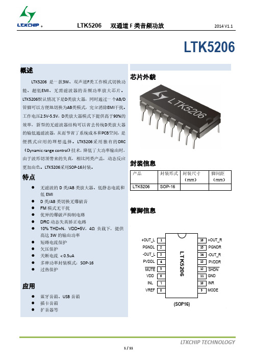
LTK5206
除了系统损耗和尺寸,滴答声和噼噗声受输入耦合电容Ci 的影响,一个大的输入耦合电容需要更多的电 荷才能到达它的静态电压(1/2VDD)。这些电荷来自经过反馈的内部电路,和有可能产生噼噗声的器件启动 端,因此,在保证低频性能的前提下减小输入电容可以减少启动噼噗声。
7、模拟参考电压端电容
输出功率
THD+N 总谐波失真加噪声 PSRR 电源电压抑制比
THD+N=10%, f=1kHz VDD=5V
RL=4Ω;
VDD=3.6V
VDD=3V
TRL=4Ω;
VDD=3.6V
VDD=3V
THD+N=10%, f=1kHz VDD=5V
RL=3Ω;
VDD=3.6V
Rf = 195kΩ(内置) Rs = 6.5kΩ(内置)
470uF
2uF
2uF
2uF
0.1uF Ri INL
1uF
0.1uF Ri INR
SHDN
MUTE
6 VDD 7 INL
8 VREF
10 INR
12 SHDN
5 MUTE
4 PVDD
13 PVDD
1 -OUT_L
3 +OUT_L
LTK5206 +OUT_R 14
工作电压2.5V-5.5V,D类放大器模式下提供高于90%的
效率,新型的无滤波器结构可以省去传统D类放大器
的输低通滤波器,从而节省了系统成本和PCB空间,是
便 携 式 应 用 的 理 想 选 择 。 LTK5206 采 用 独 有 的 DRC
(Dynamic range control)技术,降低了大功率输出时,
mic5205

mic5205(一)芯片简介1.1 芯片的基本介绍MIC5205是一种有效的噪声输出线性稳压器,具有非常低的压差(通常在轻负载17mV 和165mV 150毫安),和非常低接地电流(耗电600μA 输出100mA 时)。
MIC5205提供了更好的超过1%的初始精度。
专门为手持式设计的电池驱动的设备,MIC5205包括CMOS 或TTL 兼容开启/关闭控制输入。
当突然断电时,其功耗降低到近似为零,差电流调节器地面将略有增加,进一步延长电池寿命。
1.2 芯片应用时应注意绝对最大额定值:电源输入电压(V IN ) V Vto 2020+- 使能输入电压(V EN ) V Vto 2020+- 功耗(P D ) 内部限制引线温度(焊接)260?C 结温(T J ) . –40?C to +125?C 贮藏温度(T S ) -65?C to +150?C 工作额度:输入电压(V IN ) +2.5V to +16V使能输入电压(V EN ) 0V to IN V结温–40?C to +125?C 热电阻 SOT-23-5 (θJA )根据以上的描述我们在应用芯片时应注意其允许通过的最大电压电流,从而能使芯片在安全的环境下工作而不会被烧毁。
1.3 芯片的主要特点超低噪声输出 ?高输出电压精度 ?保证150mA 输出 ?低静态电流低压差电压极其精确的负载和线路调整?非常低的温度系数?电流和热限制?反向电池保护?‘零’关模式电流 ?逻辑控制电子使能1.4电气特性T C C T V V uF C uA I V V V J J EN L L O U T IN 00012540;25;0.2;0.1;100;1+≤≤-=≥==+=符号参数条件MIN Typic Max Units 0V输出电压精度随着指定的VOUT 的变化而变化 -1 -21 2 % %T V ??/0输出电压温度系数Note440C ppm 0/00/V V ?线性特性VV V O U T IN 1+=到16V0.004 0.012 0.05%/v %/v 00/V V ?负载调整mA I L 1.0=到150mA Note50.02 0.2 0.5% %0V V IN -电压差Note6mAI mA I mA I uA I L L L L 150********==== 16514011010 350 2753002502301507050m Vm V m V m V m V m V m V m VI GND接地引脚电流V EN ≥ 2.0V,I L = 100μAI L = 50mAI L = 100mAI L = 150mA 80 350 600 1300125 150 600 800 1000 1500 1900 2500μA μA μA μA μA μA μA μA μAPSRR文波抑制frequency = 100Hz, I L = 100μA75 dBI LIMIT电流限制V OUT = 0V320 500 mAVO /?P D热调节 Note8 0.05HZ nV /e no输出噪声I L = 50mA, C L =2.2μF,470pF from BYP to GND260使能输出V IL使能输入逻辑低电压稳压器关闭0.40.18VVV IH使能输入逻辑高电压稳压器开启2.0VI ILI IH使能输入流V IL ≤ 0.4V V IL ≤ 0.18V V IH = 2.0VV IH = 2.0V 20.015–1 –2 2025μA μA μA μA注意1:超越的绝对最大额定值可能会损坏设备。
才茂 CM520-6X 系列路由器说明书

厦门才茂CM520-6X系列路由器说明书厦门才茂通信科技有限公司厦门市集美区软件园三期诚毅北大街63号901、904单元电话:传真:邮政编码:361009网址:版权所有2003-2021版权声明:本使用说明书包含的所有内容均受版权法的保护,未经厦门才茂通信科技有限公司的书面授权,任何组织和个人不得以任何形式或手段对整个说明书和部分内容进行复制和转载,并不得以任何形式传播。
商标声明:注意:由于产品版本升级或其他原因,本文档内容会不定期进行更新。
除非另有约定,本文档仅作为使用指导,本文档中的所有陈述、信息和建议不构成任何明示或暗示的担保。
特别声明:产品说明书上的建议配置或者默认配置,不代表合适配置,客户须根据自己业务需要情况,调整成为适应自己业务开展的配置。
产品出厂的配置参数,仅供用户参考,用户收到设备时,不管有没有其他约定,用户必须全部检查一遍,并须根据自己项目和业务需求,自行调整配置好相关参数。
由于参数配置不当或者错误导致的问题,我司不承担任何责任。
同时,用户需要加强病毒攻击防范工作,因为病毒攻击导致的通信异常,我司不承担任何责任。
版本说明:文档版本修改说明发布日期作者V1.0第一次正式发布2017-10-11cyqV1.1添加5G说明2020-07-10ZhengfhV1.2部分功能说明更新2020-01-22Zhengfh目录第一章产品简介 (6)1.1产品概述 (6)1.2产品图片 (6)1.3产品命名规则 (7)1.4产品列表 (8)1.5产品特点 (9)1.6软件功能 (11)1.7硬件参数 (13)1.8指示灯说明 (22)第二章安装说明 (23)2.1装箱清单 (23)2.2产品说明 (23)2.3SIM卡安装 (24)2.4天线安装 (24)第三章快速配置 (25)3.1拨号上网(PPPOE disable)模式 (26)3.1.1先将SIM卡插入网关SIM卡座 (26)3.1.2连接好天线 (26)3.1.3无线网关与PC硬件连接 (27)3.1.4PC端网络设置(配置IP地址,网关,DNS) (27)3.1.5配置WAN信息 (29)3.1.6上网测试设备 (30)3.2WAN口上网(Wan APclient)模式 (30)3.2.1接好天线 (31)3.2.2网关设备WAN口通过以太网线与广域网相连 (31)3.2.3PC端网络配置(IP、网关、DNS) (31)3.2.4配置WAN信息 (31)3.2.5LAN配置 (32)3.2.6上网测试设备 (32)3.3技术支持 (32)第四章详细参数设置 (33)4.1网络配置 (33)4.1.1WAN配置 (33)4.1.2LAN配置 (37)4.1.3WiFi配置 (38)4.1.4DHCP配置 (43)4.1.5VLAN配置 (44)4.2高级配置 (45)4.2.1静态路由 (45)4.2.2NAT/DMZ (48)4.2.3在线保持 (50)4.2.4带宽管理 (51)4.3VPN应用 (52)4.3.1PPTP (52)4.3.2IPSEC/L2TP (54)4.3.3OPENVPN (57)4.3.4N2N (59)4.4运营管理 (60)4.4.1WiFidog认证配置 (60)4.4.2应用层过滤 (60)4.4.3如影随形 (62)4.4.4场站更新 (63)4.4.5本地推送 (64)4.5网络服务 (65)4.5.1动态DNS (65)4.5.2花生壳内网版 (66)4.5.3流量监控 (69)4.6设备管理 (70)4.6.1状态查询 (70)4.6.2日志信息 (71)4.6.3版本升级 (72)4.6.4WIFI探帧 (72)4.6.5电源管理 (74)4.6.6GPS信息 (75)第五章常见问题 (76)1.频繁上下线 (76)2.忘记密码 (76)N灯不亮 (76)4.无法拨号上网 (76)5.已经拨号上网,但无法打开网页 (76)附录1使用ssh登录网关命令行终端 (77)附录2使用串口登录网关命令行终端 (79)附录3恢复出厂设置 (82)附录4无线网络基本信息 (82)附录5根据网关获取的DNS设置 (83)第一章产品简介1.1产品概述设备WIFI2.4GHz和5GHz信道选择,同时系统加载了广域网通信VPN隧道、WIFI局域网传输的安全认证等安全功能,实现无线局域网和无线广域网的无缝连接,为用户提供高速、安全、可靠的移动宽带服务。
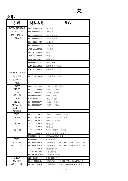
欠料表
欠 料5562CD068100DA头套固定座下盖烤漆对象内5571CD068200DA头套固定座上盖烤漆印字 L5571CD068300DA头套固定座上盖烤漆印字 R5A04CD06850000说明书对象内5A07CD068B0010外箱贴标对象内5A07CD068G0000内箱贴标对象内5A094402202200内箱 A3A5A104554554600外箱 A=A5B23CD06820000透明盒对象内5D18CD068C0000绒布袋(非移形)对象内5D69CD06870000头套 (冲孔) 对象内TW094 EM-85420EM00804000边网300 2/65418EM00800000前网TW094 EM-856U307D001DL10070排线座1PIN/EM-858U540 2/65203DM858000DA头段烤平光黑对象内5205D856U1000A本体后段组立加工5419E858U01800后网+内网5508E858U00000本体底座对象内5524E858U00000固定架 EM-858U5535YH00800000夹子下座对象内5535YH00910000夹子上座对象内5612YH00900000防滑套 (夹子上座用)5623EM860U0000音头固定座 (硬度50度+-5)5A105153852150外箱 A=A 对象内TW0235D69CD08500000头套(依图标)ANC-3505B151102800030PE袋500 2/65B154003300030PE 袋5C12NC35000000EVA 单面背胶TW023*******R3R5PG0变换插头 (ANC-350) 金ANC-3503112TS0060AP00MIC头+基板加工(配对包装500 2/1331541R50000010电池对象内318ANC3502000A基板套件 (双面板)5502AN350500DA右耳壳饰盖烤漆对象内5B151000500030塑料袋对象内5B151102800030PE袋对象内5B154003300030PE 袋对象内5C12NC35000000EVA 单面背胶对象内5D18CD09800000皮袋(两条拉绳)HA-04 :2025647HA00400000橡胶(HA-04)黑色料 表CD-68 烤黑灰色(BLACK 7C)+皮革353PCS610-131212392000 CD-68 烤黑灰色(BLACK 7C)+皮革+印黑字对象内0PCS610-131212391000 CD-68 烤黑灰色(BLACK 7C)+皮革+印黑字对象内80PCS610-131212391000 F38 INCIPIO103PCS610-131212381000 INCIPIO NX-100 (新版)1205 含净重毛重275PCS610-131******** NX-100 含净重毛重225PCS610-131******** 440*220*220mm(单坑)0PCS610-131******** 455*455*460mm(双坑)0PCS610-1312123850 F38 INCIPIO57PCS610-131212381000 CD-68 INCIPIO 灰色203PCS610-131212381000 CD-68 黑色482PCS610-131212391000260623 DL1007#26A2.541P单向含头《CG50131060》300PCS610-131******** 62*56*74.5(锌合金)《BA0858U100》38PCS610-131******** A99JB ProSound0PCS610-131******** EM-858U双层铁网烤铁灰色《AA08580102》117PCS610-131******** EM-858U MS-D07(不附螺帽《BE0858U000》479PCS610-131******** 54.6*48.6*25.5 对象内《CH0858U000》72PCS610-131******** YH-8 (含铜螺母)《LAYH800002》397PCS610-131******** YH-9《LAYH090001》292PCS610-131******** YH-9 黑色对象内《ABYH090000》390PCS610-131******** EM-860U 黑色矽胶 对象内51PCS610-131******** EM-856U 527*427*235 mm0PCS610-1312112145 (黑色无纹软皮)CD-85《CY00850000》993 (开口) 11x28cm t=0.03mm《HT05860000》857 40*33cm 开口 T=0.03mm《HT04033000》279 L22xW12.2x2t(附背胶)《DM22120202》467 2*3.5PLUG 转3.5 插座《EN02030500》418PCS610-131******** TS-60AP(-40+/-2dB)对象内《CATS-60AP0》135PCS610-131******** 4号(AAA 7号)《HE00400000》215PCS610-131******** ANC-350 对象内《CZANC35002》-471PCS610-131******** ANC-350 烤黑色+印灰字+皮革304PCS610-131******** 10CM*5CM(开口)0.03mm《HT00501000》212PCS610-131******** (开口) 11x28cm t=0.03mm《HT05860000》-857PCS610-131******** 40*33cm 开口 T=0.03mm《HT04033000》-297PCS610-131******** L22xW12.2x2t(附背胶)《DM22120202》-467PCS610-131********空白(材质同PHX) 对象内《KWCD980000》400PCS610-131********329。
ZM602系列Wi-Fi模块用户手册说明书
ZM602系列Wi-Fi模块用户手册Wi-Fi模块UM01010101 1.2 Date:2022/9/16类别内容关键词ZM602模块,Wi-Fi+BLE,用户手册摘要©2022 Guangzhou ZHIYUAN Electronics Co., Ltd.修订历史文档版本日期原因V1.00 2022.04.25 首次发布V1.01 2022.08.18 新增产品实物图;新增特色功能说明;更新产品选型表;优化快速使用说明;优化BLE数据透传说明;新增数据通道说明;新增串口命令:读取设备MAC地址、读取STA连接状态、读取连接到本设备的STA列表目录1. 产品简介 (1)1.1 概述 (1)1.2 产品特性 (1)1.3 典型应用 (2)1.4 产品选型表 (2)2. 快速使用说明 (3)2.1 与设备建立连接 (3)2.2 设置Wi-Fi工作模式 (4)2.3 使用设备连接其他热点 (5)3. 产品功能 (7)3.1 Wi-Fi数据透传 (7)3.1.1 场景一:模块数据互传 (7)3.1.2 场景二:模块与笔记本电脑进行数据互传 (12)3.2 BLE数据透传 (13)4. 工作模式 (16)4.1 网络工作模式 (16)4.1.1 数据通道 (16)4.1.2 TCP Server模式 (17)4.1.3 TCP Client模式 (18)4.1.4 UDP Client模式 (18)4.1.5 UDP Server模式 (18)4.1.6 MQTT Client模式 (19)4.2 Wi-Fi工作模式 (19)4.2.1 AP模式 (19)4.2.2 STA模式 (19)4.2.3 AP+STA模式 (19)5. 配置设备 (20)5.1 网页配置 (20)5.1.1 登录设备网页 (20)5.1.2 系统 (20)5.1.3 专家 (20)5.1.4 串口 (20)5.1.5 网络 (21)5.1.6 无线 (21)5.1.7 热点 (22)5.1.8 用户登录 (22)5.1.9 系统管理 (22)5.1.10 软件更新 (22)5.2 蓝牙快速配网 (23)5.3 串口协议指令 (25)5.3.1 基本原则 (25)5.3.2 封包结构 (26)5.3.3 命令列表 (28)5.3.4 事件列表 (28)5.3.5 命令解析 (29)6. 免责声明 (42)ZM602系列Wi-Fi模块用户手册Wi-Fi模块1.产品简介1.1 概述ZM602系列Wi-Fi模块是广州致远电子股份有限公司基于博流BL602系列芯片开发的高性能Wi-Fi+BLE模块产品。
构建pc104上的linux系统平台
构建PC104上的嵌入式Linux系统平台构建PC104上的嵌入式Linux系统平台为了适应目前嵌入式系统操作平台在性能、成本、可靠性等各方面的要求,论述了以Linux作为操作系统平台的优势,分析了以PC104卡和CompactFlash卡构造带图形用户界面(GUI)的Linux系统的关键技术.0 前言嵌入式系统的商品化操作系统十分丰富,如Palm OS、VxWorks、pSOS、Neculeus和Windows CE等。
高端嵌入式系统要求许多高级的功能,但其价格也相对昂贵,一般用户难以接受。
微软的Windows CE也有此类功能,却不具备大多数嵌入式系统要求的实时性能,而且难以移植。
Linux为嵌入式系统提供了一个极有吸引力的选择,对于嵌入式系统而言,性能、成本和可靠性是最至关重要的三个因素。
首先,众多文献资料表明,Linux是当前可获得的最简捷、最快速的操作系统,其性能优越之处,是把图形处理为一个用户级的应用,图形可根据需要被选择是否运行。
Linux系统中存在适度复杂的图形界面,但是它们并没有与操作系统的内核紧紧捆绑在一起,图形界面可按需求关闭。
这样就可以在Linux内核上运行专门为嵌入式系统定制的图形系统,从而获得优越的性能。
其次,Linux系统源代码完全公开,可以用非常便宜的价格得到各种Linux分发版,不必考虑许可成本,将用户从许可证的限制中解脱出来,无需去为资金短缺而烦忧。
Linux能正常运行于内存缺乏,容量紧张的系统中,减少在硬件升级上的开支。
另外,在系统稳定性方面,Linux几乎不崩溃,Linux的稳定性是由于它没有像其它操作系统一样内核极其庞大。
考察资料表明,Linux与其它Unix系统和大型操作系统如VMS、IBM大型机等一样具有相同的可靠性。
在上述优势之外,Linux还拥有众多硬件支持的特点和强大的网络支持功能。
正因为Linux在价格、性能、稳定性以及用户定制等方面的突出优势,用它来构建系统操作平台是一个很不错的解决方案。
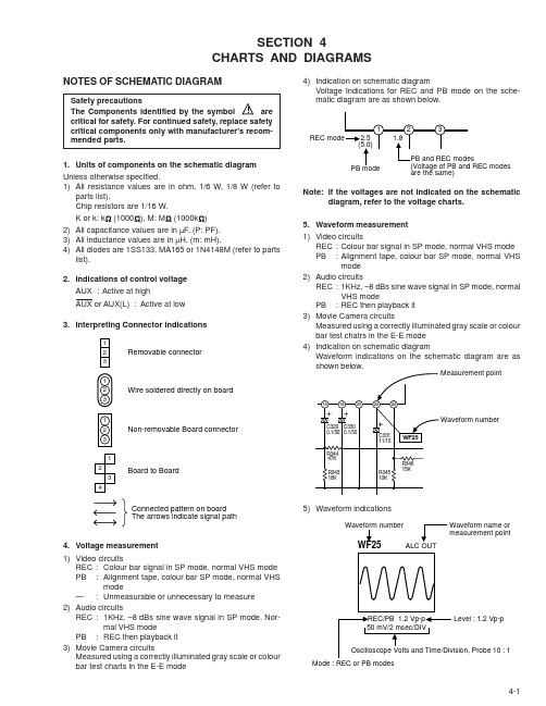
JVC SR-VS30E service manual 维修手册 电路图
J902
AV1
J901
AV2/DECODER
CN502 GND
D_DUB_C_IN GND
D_DUB_Y_IN GND
C_TO_DIGI GND
Y/V_TO_DIGI GND
Y_FROM_DIGI GND
C_FROM_DIGI GND
TO_PS_C TO_PS_Y
CN503 R_V_OUT GND S_Y_OUT GND S_C_OUT GND FRONT_C_IN GND C.BOX/SAT_CTL CN504 V_FROM_AV EE[L] REC_COLOR GND FROM_PS_C GND I2C_DATA_A/V I2C_CLK_A/V SW5V Fsc CN505 V_TO_OSD CHARA_DATA2 GND V_FROM_OSD GND FROM_PS_Y GND Y_FROM_S.E GND Y_TO_S.E GND Y_TO_AV CN506 PB_COLOR FRONT_Y_IN SECAM_PB_COLOR MAIN_ALC_DET Y_TO_SUB P.MUTE[L] FRONT_V_IN GND Y_OUT GND C_OUT CN902 P50_I/O SCR[H] 3.58NTSC[H]/P.ON_P TU_VIDEO CH+12V SW12V I2C_CLK2 I2C_DATA2 GND
C : Chip component (D : Discrete component)
Horizontal “A” zone Vertical “6” zone
Note: For general information in service manual, please refer to the Service Manual of GENERAL INFORMATION Edition 4 No. 82054D (January 1994).
LED屏驱动IC-BMI5026中文资料
聚积科技 2006 台湾新竹市埔顶路 18 号 6F 之四 电话:+886-3-579-0068,传真:+886-3-579-7534 E-mail: info@ -1-
2006 年 4 月,VA.02
MBI5026
16 位恒流 LED 驱动器
功能方块图
OUT0 OUT1 OUT14 OUT15
CLK讯号的最大爬升时间 CLK讯号的最大下降时间
电流输出埠的电位爬升时间 电流输出埠的电位下降时间
**如果是以多颗 IC 串联方式连接使用,若 tr 与 tf 值太大(>500 ns),可能会难以达成数据传输所要的时序要求。
动态特性的测试电路
IDD
IOUT
OUT0
VIH, VIL
VDD OE CLK LE
使LED不亮
-4-
2006 年 4 月,VA.02
MBI5026
16 位恒流 LED 驱动器
最大限定范围
特性 电源电压 输入端电压 输出端电流 输出端耐受电压 时钟频率 接地端电流 代表符号 最大工作范围 单位
VDD VIN IOUT VDS FCLK IGND CN CNS CD CF CP CPA CN CNS CD CF CP CPA GN GNS GD GF GP GPA GN GNS GD GF GP GPA Topr Tstg Rth(j-a) PD 1.80 1.50 2.01 1.69 1.38 1.38 55.52 66.74 49.81 59.01 72.43 72.43
Macroblock 特色
z z z 16 个恒流输出通道 恒流输出值不受输出端负载电压影响 极为精确的电流输出值, 通道间最大差异值:<±3%; 芯片间最大差异值:<±6%。 z z z z z z z 利用一个外接电阻,可调整电流输出值 恒流输出范围值:5 - 90 mA
RF211(1)
MICRF506410MHz and 450MHz ISM BandTransceiverGeneral DescriptionThe MICRF506 is a true single-chip, frequency shift keying(FSK) transceiver intended for use in half-duplex,bidirectional RF links. The multi-channeled FSK transceiveris intended for UHF radio equipment in compliance with theEuropean Telecommunication Standard Institute (ETSI)specification, EN300 220.The transmitter consists of a PLL frequency synthesizerand power amplifier. The frequency synthesizer consists ofa voltage-controlled oscillator (VCO), a crystal oscillator,dual modulus prescaler, programmable frequency dividers,and a phase-detector. The loop-filter is external for flexibilityand can be a simple passive circuit. The output power ofthe power amplifier can be programmed to seven levels. Alock-detect circuit detects when the PLL is in lock. Inreceive mode, the PLL synthesizer generates the localoscillator (LO) signal. The N, M, and A values that give theLO frequency are stored in the N0, M0, and A0 registers.The receiver is a zero intermediate frequency (IF) typewhich makes channel filtering possible with low-power,integrated low-pass filters. The receiver consists of a lownoise amplifier (LNA) that drives a quadrature mix pair. Themixer outputs feed two identical signal channels in phasequadrature. Each channel includes a pre-amplifier, a thirdorder Sallen-Key RC low-pass filter that protects thefollowing switched-capacitor filter from strong adjacentchannel signals, and a limiter. The main channel filter is aswitched-capacitor implementation of a six-pole elliptic lowpass filter. The cut-off frequency of the Sallen-Key RC filtercan be programmed to four different frequencies: 100kHz,150kHz, 230kHz, and 340kHz. The I and Q channeloutputs are demodulated and produce a digital data output.The demodulator detects the relative phase of the I and theQ channel signal. If the I channel signal lags behind the Qchannel, the FSK tone frequency is above the LOfrequency (data '1'). If the I channel leads the Q channel,the FSK tone is below the LO frequency (data '0'). Theoutput of the receiver is available on the DataIXO pin. Areceive signal strength indicator (RSSI) circuit indicates thereceived signal level. All support documentation can befound on Micrel’s web site at .RadioWire®Features•True single chip transceiver•Digital bit synchronizer•Received signal strength indicator (RSSI)•RX and TX power management•Power down function•Reference crystal tuning capabilities•Basedband shaping•Three-wire programmable serial interface•Register read back functionApplications•Telemetry•Remote metering•Wireless controller•Remote data repeater•Remote control systems•Wireless modem•Wireless security systemRadioWire® RF Transceiver Selection GuideDevice Frequency Range MaximumData Rate ReceiveSupplyCurrent TransmitModulationType PackageMICRF500700MHz – 1.1GHz128k Baud12mA 2.5 to 3.4V50mA FSK LQFP-44 MICRF501300MHz – 440MHz128k Baud8mA 2.5 to 3.4V45mA FSK LQFP-44 MICRF505850MHz – 950MHz200k Baud13mA 2.0 to 2.5V28mA FSK MLF™-32 MICRF506410MHz – 450MHz200k Baud12mA 2.0 to 2.5V21.5mA FSK MLF™-32Ordering InformationPart Number Junction Temp. Range(1)PackageMICRF506BML–40° to +85°C32-Pin MLF TM____________________________________________________________________________________________________ Typical ApplicationANT222MICRF506 – MLF32Pin ConfigurationRFGND PTATBIAS RFVDD RFGNDANT RFGND GND NC XTALOUT XTALIN CS SCLK IODATAIXO DATACLK NCG N D V A R I N V C O G N D V C O V D D N C C P O U T D I G G N D D I G V D DQ C H O U T I C H O U T I F G N D I F V D D C I B I A S R S S I L D N C32-Pin MLF TMPin DescriptionPin NumberPin Name TypePin Function 1RFGND LNA and PA ground.2PTATBIAS O Connection for bias resistor.3RFVDD LNA and PA power supply.4RFGND LNA and PA ground.5ANT I/O Antenna In/Output.6RFGND LNA and PA ground.7RFGND LNA and PA ground.8NC No connect.9CIBIAS O Connection for bias resistor.10IFVDD IF/mixer power supply.11IFGND IF/mixer ground.12ICHOUT O Test pin.13QCHOUT O Test pin.14RSSI O Received signal strength indicator.15LD O PLL lock detect.16NC No connect.17NCNo connectPin Number Pin Name Type Pin Function 18DATACLK O RX/TX data clock output.19DATAIXOI/O RX/TX data input/output.20IOI/O3-wire interface data in/output.21SCLK I/O 3-wire interface serial clock.22CSI3-wire interface chip select.23XTALIN I Crystal oscillator input.24XTALOUT OCrystal oscillator output.25DIGVDD Digital power supply.26DIGGND Digital ground.27CPOUTO PLL charge pump output.28GND Substrate ground.29VARIN IVCO varactor.30VCOGND VCO ground.31VCOVDD VCO power supply.32NCNo connect.Absolute Maximum Ratings (1)Supply Voltage (V DD )............................................+3.3VVoltage on any pin (GND = 0V)........-0.3V to 2.7V Lead Temperature (soldering, 4sec.)................TBD°C Storage Temperature (T s ).................-55°C to +150°C EDS Rating (3)...........................................................2kVOperating Ratings (2)Supply voltage (V IN )..............................+2.0V to +2.5V RF Frequencies............................410MHz to 450MHz Data Rate (NRZ).........................................<200kBaud Ambient Temperature (T A )..................–40°C to +85°C Package Thermal ResistanceMLF TM ( JA )..............................................41.7°C/WElectrical Characteristics (4)f RF = 433MHz. Data-rate = 125kbps, Modulation type = closed-loop VCO modulation, V DD = 2.5V; T A = 25°C, bold values indicate –40°C< T A < +85°C, unless noted.SymbolParameterConditionMin TypMax Units RF Frequency Operating Range 410450MHz Power Supply 2.02.5V Power Down Current 0.33µA Standby Current280370µAVCO and PLL SectionReference Frequency 440MHz 433.75MHz to 434.25MHz 0.7 1.3ms PLL Lock Time 3kHz bandwidth 430MHz to 440MHz 1.32ms PLL Lock Time (5)20kHz bandwidth 433.75MHz to 434.25MHz 0.3ms Rx – Tx 1.0 1.4ms Tx – Rx 1.0 2.5ms Standby Rx 1.03ms Switch Time3kHz loop bandwidthStandby Tx1.0ms Crystal Oscillator Start-Up Time 16MHz, 9pF load, 5.6pF loading capacitors1.0ms VCP OUT = 1.1V, CP_HI = 010*******µA Charge Pump CurrentVCP OUT = 1.1V, CP_HI = 1420500680µATransmit SectionR LOAD = 500 , Pa2-0-11111dBm Output PowerR LOAD = 500 , Pa2-0-001-7dBm Over temperature range 1dB Output Power Tolerance Over power supply range 3dB R LOAD = 500 , Pa2-0-11121.5mA R LOAD = 500 , Pa2-0-00110.5mA Tx Current ConsumptionR LOAD = 500 , Pa2-0-0008.0mA Binary FSK Frequency Separation (5)Birate = 200kbps 20500kHz VCO modulation 20200kbps Data Rate (5)Divider modulation20kbpsSymbol Parameter Condition Min Typ Max Units Occupied bandwidth(5)38.4kbps, = 2, 20dBc140kHz125kbps, = 2, 20dBc550kHz200kbps, = 2, 20dBc800kHz 2nd Harmonic-16dBm 3rd Harmonic-8dBm Spurious Emission<1GHz(5)<-54dBm Spurious Emission<1GHz(5)<-30dBm Receive SectionRx Current Consumption12mALNA bypass9.5mASwitch cap filter bypass with LNA9.5mA Rx Current Consumption Variation Over temperature3mA Receiver Sensitivity 2.4kbps, = 16-113dBm4.8kbps, = 16-111dBm19.2kbps, = 4-106dBm38.4kbps, = 4-104dBm76.8kbps, = 2-101dBm125kbps, = 2-100dBm200kbps, = 2-97dBm Receiver Maximum Input Power125kbps, 125kHz deviation+12dBm20kbps, 40kHz deviation+2dBm Receiver Sensitivity ToleranceOver temperature4dBOver power supply range1dB Receiver Bandwidth50350kHz Co-Channel Rejection T.B.D.dB Adjacent Channel Rejection500kHz spacing T.B.D.dB1MHz spacing T.B.D.dB Blocking±1MHz47dB±2MHz48dB±5MHz39dB±10MHz48dB Noise Figure, Cascade T.B.D.dB 1dB Compression-34dB Input IP3 2 tones with 1MHz separation-25dBm Input IP2T.B.D.dBm LO Leakage-90dBm Spurious Emission(5)<1GHz<-57dBm>1GHz<-57dBm Input Impedance(5)50Symbol Parameter Condition Min Typ Max Units RSSI Dynamic Range50dBPin = -110dBm0.9V RSSI Output RangePin = -60dBm2V Digital Inputs/OutputsVIH Logic Input High0.7VDDVDDVVILLogic Input Low00.3VDDV Clock/Data Frequency(5)10MHz Clock/Data Duty Cycle(5)4555% Notes:1. Exceeding the absolute maximum rating may damage the device.2. The device is not guaranteed to function outside its operating rating.3. Devices are ESD sensitive. Handling precautions recommended. Human body model, 1.5k in series with 100pF.4. Specification for packaged product only.5. Guaranteed by design.Programming GeneralThe MICRF506 functions are enab led through a number of programming bits. The programming bits are organized as a set of addressab le control registers, each register holding 8 bits.There are 23 control registers in total in the MICRF506, and they have addresses ranging from 0 to 22. The user can read all the control registers. The user can write to the first 22 registers (0 to 21); the register 22 is a read-only register.All control registers hold 8 bits and all 8 bits must be written to when accessing a control register, or they will be read. Some of the registers do not utilize all 8 bits. The value of an unused bit is “don’t care.”The control register with address 0 is referred to as ControlRegister0, the control register with address 1 is ControlRegister1 and so on. A summary of the control registers is given in the tab le b elow. In addition to the unused bits (marked with”-“) there are a numb er of fixed b its (marked with “0” or “1”). Always maintain these as shown in the table.The control registers in MICRF506 are accessed through a 3-wire interface; clock, data and chip select. These lines are referred to as SCLK, IO, and CS, respectively. This 3-wire interface is dedicated to control register access and is referred to as the control interface. Received data (via RF) and data to transmit (via RF) are handled b y the DataIXO and DatalClk (if enabled) lines; this is referred to as the data interface.The SCLK line is applied externally; access to the control registers are carried out at a rate determined by the user. The MICRF506 will ignore transitions on the SCLK line if the CS line is inactive. The MICRF506 can b e put on a b us, sharing clock and data lines with other devices.All control registers should b e initiated (written to) following a power-on. During operation, however, writing to one register is sufficient to change the way the transceiver works.Adr DataA6…A0D7D6D5D4D3D2D1D0 0000000LNA_by PA2PA1PA0Sync_en Mode1Mode0Load_en 0000001Modulation1Modulation2ol_opamp_en‘0’RSSI_en LD_en PF_FC1PF_FC0 0000010CP_HI‘0’‘0’PA_By OUTS3OUTS2OUTS1OUTS0 0000011‘1’‘1’‘0’VCO_IB2VCO_IB1VCO_IB0VCO_freq1VCO_freq0 0000100Mod_F2Mod_F1Mod_F0Mod_I4Mod_I3Mod_I2Mod_I1Mod_I0 0000101--‘0’‘1’Mod_A3Mod_A2Mod_A1Mod_A0 0000110-Mod_clkS2Mod_clkS1Mod_clkS0BitSync_clkS2BitSync_clkS1BitSync_clkS0BitRate_clkS2 0000111BitRate_clkS1BitRate_clkS0RefClk_K5RefClk_K4RefClk_K3RefClk_K2RefClk_K1RefClk_K0 0001000‘1’ScClk_X2ScClk5ScClk4ScClk3ScClk2ScClk1ScClk0 0001001‘0’‘1’‘1’XCOtune4XCOtune3XCOtune2XCOtune1XCOtune0 0001010--A0_5A0_4A0_3A0_2A0_1A0_0 0001011----N0_11N0_10N0_9N0_8 0001100N0_7N0_6N0_5N0_4N0_3N0_2N0_1N0_0 0001101----M0_11M0_10M0_9M0_8 0001110M0_7M0_6M0_5M0_4M0_3M0_2M0_1M0_0 0001111--A1_5A1_4A1_3A1_2A1_1A1_0 0010000----N1_11N1_10N1_9N1_8 0010001N1_7N1_6N1_5N1_4N1_3N1_2N1_1N1_0 0010010----M1_11M1_10M1_9M1_8 0010011M1_7M1_6M1_5M1_4M1_3M1_2M1_1M1_0 0010100‘1’‘0’‘1’‘1’‘0’‘1’‘0’‘1’0010101----FEEC_3FEEC_2FEEC_1FEEC_0 0010110FEE_7FEE_6FEE_5FEE_4FEE_3FEE_2FEE_1FEE_0Table 1. Control Registers in MICRF506Names of programming bits, unused bits (“-“) and fixed bits (“1” or “0”) are shown. The control register with address 0 is referred to asControlRegister0 etc.Writing to the control registers in MICRF506Writing: A number of octets are entered into MICRF506 followed by a load-signal to activate the new setting. Making these events is referred to as a “write sequence.” It is possible to update all, 1, or n control registers in a write sequence. The address to write to (or the first address to write to) can be any valid address (0-21). The IO line is always an input to the MICRF506 (output from user) when writing. What to write:•The address of the control register to write to (or if more than 1 control register shouldbe written to, the address of the 1st controlregister to write to).• A bit to enable reading or writing of the control registers. This bit is called the R/Wbit.•The values to write into the control register(s).What to write:Field CommentsAddress: A 7-bit field, ranging from 0 to 21. MS B is written first.R/W bit: A 1-bit field, = “0” for writingValues: A number of octets (1-22 octets). MS B in every octet is written first. The first octet iswritten to the control register with thespecified address (=”Address”). The nextoctet (if there is one) is written to the controlregister with address = “Address + 1” and soon.Table 2.How to write:Bring CS active to active to start a write sequence. The active state of the CS line is “high.” Use the S CLK/IO serial interface to clock “Address” and “R/W” bit and “Values” into the MICRF506. MICRF506 will sample the IO line at negative edges of S CLK. Make sure to change the state of the IO line before the negative edge. Refer to figures below.Bring CS inactive to make an internal load-signal and complete the write-sequence. Note: there is an exception to this point. If the programming bit called “load_en” (bit0 in ControlRegister0) is “0”, then no load pulse is generated.The two different ways to “program the chip” are:•Write to a number of control registers (0-22) when the registers have incrementaladdresses (write to 1, all or n registers)•Write to a number of control registers when the registers have non-incrementaladdresses.Writing to a Single RegisterWriting to a control register with address “A6. A5,…A0” is described here. During operation, writing to 1 register is sufficient to change the way the transceiver works. Typical example: Change from receive mode to power-down.What to write:Field CommentsAddress:7 bit = A6, A5, …A0 (A6 = msb. A0 = lsb)R/W bit:“0” for writingValues:8 bits = D7, D6, …D0 (D7 = msb, D0 = lsb)Table 3.“Address” and “R/W bit” together make 1 octet.In addition, 1 octet with programming bits is entered. In total, 2 octets are clocked into the MICRF506.How to write:•Bring CS high•Use SCLK and IO to clock in the 2 octets•Bring CS lowCSIOFigure 1.In Figure 1, IO is changed at positive edges of SCLK. The MICRF506 samples the IO line at negative edges. The value of the R/W bits is always “0” for writing.Writing to All RegistersAfter a power-on, all writable registers should be written. This is described here.Writing to all register can be done at any time. To get the simplest firmware, always write to all registers. The price to pay for the simplicity is increased write-time, which leads to increased time to change the way the MICRF506 works.What to writeField CommentsAddress:‘000000’ (address of the first register to write to, which is 0)R/W bit:“0” for writingValues:1st O c t e t:w a n t e d v a l u e s f o r ControlR egister0. 2nd Octet: wanted valuesfor ControlRegister1 and so on for all of theoctets. So the 22nd octet wants values forControlR egister21. R efer to the specificsections of this document for actual values.Table 4.“Address” and “R/W bit” together make 1 octet.In addition, 22 octets with programming bits are entered. In total, 23 octets are clocked into the MICRF506.How to write:•Bring CS high•Use SCLK and IO to clock in the 23 octets•Bring CS lowRefer to the figure in the next section, “Writing to n registers having incremental addresses”.Writing to n Registers having Incremental AddressesIn addition to entering all bytes, it is also possible to enter a set of n bytes, starting from address i = “A6, A5, … A0”. Typical example: Clock in a new set of frequency dividers (i.e. change the R F frequency).“Incremental addresses”. Registers to be written are located in i, i+1, i+2.What to writeField CommentsAddress:7 bit = A6, A5, …A0 (A6 = msb. A0 = lsb) (address of first byte to write to)R/W bit:“0” for writingValues:n* 8 bits =D7, D6, …D0 (D7 = msb, D0 = lsb) (writtento control reg. with address ”i”)D7, D6, …D0 (D7 = msb, D0 = lsb) (writtento control reg. with address ”i+1”)D7, D6, …D0 (D7 = msb, D0 = lsb) (writtento control reg. with address ”i+n-1”)Table 5.“Address” and “R/W bit” together make 1 octet.In addition, n octets with programming bits are entered. Totally, 1 +n octets are clocked into the MICRF506.How to write:•Bring CS high•Use SCLK and IO to clock in the 1 + n octets•Bring CS lowIn Figure 1, IO is changed at positive edges of SCLK. The MICR F506 samples the IO line at negative edges. The value of the R/W bits is always “0” for writing.CSIOFigure 2.Writing to n Registers having Non-Incremental AddressesR egisters with non-incremental addresses can be written to in one write-sequence as well. Example of non-incremental addresses: “0,1,3”. However, this requires more overhead, and the user should consider the possibility to make a “continuous”update, for example, by writing to “0,1,2,3” (writing the present value of “2” into “2”). The simplest firmware is achieved by always writing to all registers. Refer to previous sections.This write-sequence is divided into several sub-parts:•Disable the generation of load-signals by clearing bit “load_en” (bit0 inControlRegister0)•R epeat for each group of register having incremental addresses:o Bring CS activeo Enter first address for this group,R/W bit and valueso Bring CS inactiveo Finally, enable and make a load-signal by setting “load_en”Refer to the previous sections for how to write to 1 or n (with incremental addresses) registers in the MICRF506.Reading from the control registers in MICRF506 The “read-sequence” is:1.Enter address and R/W bit2.Change direction of IO line3.Read out a number of octets and change IOdirection back again.It is possible to read all, 1 or n registers. The address to read from (or the first address to read from) can be any valid address (0-22). R eading is not destructive, i.e. values are not changed. The IO line is output from the MICRF506 (input to user) for a part of the read-sequence. R efer to procedure description below.A read-sequence is described for reading n registers, where n is number 1-23.Reading n registers from MICRF506CSIOIO InputIO OutputFigure 3.In the figure, 1 register is read. The address is A6,A5, … A0. A6 = msb. The data read out is D7, D6,…D0. The value of the R/W bit is always “1” for reading.SCLK and IO together form a serial interface. SCLKis applied externally for reading as well as for writing.•Bring CS active•Enter address to read from (or the first address to read from) (7 bits) and•The R/W bit = 1 to enable reading•Make the IO line an input to the user (set pin in tristate)•Read n octets. The first rising edge of SCLK will set the IO as an output from theMICRF506. MICRF will change the IO line atpositive edges. The user should read the IOline at the negative edges.•Make the IO line an output from the user again.Programming interface timingFigure 4 and Table 6 shows the timing specification for the3-wire serial programming interface.CSSCLKIO A6A5A0RW D7D6D2D1D0Address Register Data RegisterLOADTsclTwriteTreadThighTlowTperTcsr traisetfallFigure 4.ValuesSymbol Parameter Min.Typ.Max.Units Tper Min. period ofSCLK50nsThigh Min. high time ofSCLK20nsTlow Min. low time ofSCLK20nstfall Max. time offalling edge ofSCLK1nstrise Max. time of risingedge of SCLK1nsTcsr Max. time of risingedge of CS tofalling edge ofSCLK0nsTcsf Min. delay fromrising edge of CSto rising edge ofSCLK5nsTwrite Min. delay fromvalid IO to fallingedge of SCLKduring a writeoperation0nsTread Min. delay fromrising edge ofSCLK to valid IOduring a readoperation(assuming loadcapacitance of IOis 25pF)75nsTable 6. Timing Specification for the 3-wireProgramming Interface Programming summary•Use CS, SCLK, and IO to get access to the control registers in MICRF506.•SCLK is user-controlled.•Write to the MICRF506 at positive edges (MICRF506 reads at negative edges).•Read from the MICRF506 at negative edges (MICRF506 writes at positive edges)•After power-on: Write to the complete set of control registers.•Address field is 7 bits long. Enter msb first.•R/W bit is 1 bit long (“1” for read, “0” forwrite)•Address and R/W bit together make 1 octet•All control registers are 8 bits long.Enter/read msb in every octet first.•Always write 8 bits to/read 8 bits from acontrol register. This is the case for registerswith less than 8 used programming bits aswell.•Writing: Bring CS high, write address and R/W bit followed by the new values to fill intothe addressed control register(s) and bringCS low for loading, i.e. activation of the newcontrol register values (“load_en” = 1).•Reading: Bring CS high, write address and R/W bit, set IO as an input, read presentcontents of the addressed controlregister(s), bring CS low and set IO anoutput.Frequency SynthesizerA6…A0D7D6D5D4D3D2D1D00001010--A0_5A0_4A0_3A0_2A0_1A0_00001011----N0_11N0_10N0_9N0_80001100N0_7N0_6N0_5N0_4N0_3N0_2N0_1N0_00001101----M0_11M0_10M0_9M0_80001110M0_7M0_6M0_5M0_4M0_3M0_2M0_1M0_00001111--A1_5A1_4A1_3A1_2A1_1A1_00010000----N1_11N1_10N1_9N1_80010001N1_7N1_6N1_5N1_4N1_3N1_2N1_1N1_00010010----M1_11M1_10M1_9M1_80010011M1_7M1_6M1_5M1_4M1_3M1_2M1_1M1_0The frequency synthesizer consists of a voltage-controlled oscillator (VCO), a crystal oscillator, dual modulus prescaler, programmable frequency dividers and a phase-detector. The loop-filter is external for flexibility and can be a simple passive circuit. The lengths of the N, M, and A registers are12, 12 and 6 respectively. The M, N, and A values can be calculated from the formula:fPDH =f XCO M =f VCO 31 N +A =f RF 431 N +Awhere fPhD is the phase detector comparison frequency.PhD: Phase detector comparison frequency fxco: Crystal oscillator frequencyfvco: Voltage controlled oscillator frequencyThere are two sets of each of the divide factors (i.e.A0 and A1). If modulation by using the dividers is selected (that is Modulation1=1, Modulation0=0), the two sets should be programmed to give two RF frequencies, separated by two times the specified frequency deviation. For all other modulation methods, and also in receive mode, the 0-set will be used.Crystal Oscillator (XCO)Adr D7D6D5D4D3D2D1D00001001‘0’‘1’‘1’XCOtune4XCOtune3XCOtune2XCOtune1XCOtune0The crystal oscillator is a very critical block. As the crystal oscillator is a reference for the RF output frequency and also for the LO frequency in the receiver, very good phase and frequency stability is required. The schematic of the crystal oscillator’sexternal components for 16MHz are shown in Figure 5.XT Figure 5. Crystal Oscillator CircuitThe crystal should be connected between pins XosIn and XoscOut (pin 23 and 23). In addition,loading capacitors for the crystal are required. The loading capacitor values depend on the total load capacitance, C L , specified for the crystal. The load capacitance seen between the crystal terminals should be equal to C L for the crystal to oscillate at the specified frequency.C L =11C 10+1C 11+C parasiticThe parasitic capacitance is the pin input capacitance and PCB stray capacitance. Typically,the total parasitic capacitance is around 6pF. For instance, for a 9pF load crystal the recommended values of the external load capacitors are 5.6pF.It is also possible to tune the crystal oscillator internally by switching in internal capacitance using 5 tune bits XCOtune4 – XCOtun0. When XCOtune4– XCOtune0 = 0 no internal capacitors are connected to the crystal pins. When XCOtune4 –XCOtune0 = 1 all of the internal capacitors are connected to the crystal pins. Figure 3 shows the tuning range for two different capacitor values, there are 1.5pF and no capacitors.The crystal used is a TN4-26011 from Toyocom.S pecification: Package TSX-10A, Nominal frequency16.000000 MHz, frequency tolerance ±10ppm,frequency stability ±9ppm, load capacitance 9pF,pulling sensitivity 15ppm/pF.-60,0-40,0-20,00,020,040,060,080,0100,008162432XCO bitvalue[p p m ]Figure 6. XCO TuningT he start up time is given in T able 7. As can be seen, more capacitance will slow down the start up time.T he start-up time of a crystal oscillator is typically around a millisecond. T herefore, to save current consumption, the XCO is turned on before any other circuit block. During start-up the XCO amplitude will eventually reach a sufficient level to trigger the M-counter. After counting 2 M-counter output pulses the rest of the circuit will be turned on. The current consumption during the prestart period is approximately 280µA.XCO BitvalueStart-up Time (ms)05901590270047008810161140312050Table 7. Typical values with C EXT = 1.5pFIf an external reference is used instead of a crystal,the signal shall be applied to pin 24, XtalOut. Due to internal DC setting in the XCO, an AC coupling is recommended to be used between the external reference and the XtalOut-pin.VCOA6..A0D7D6D5D4D3D2D1D00000011‘1’‘1’‘0’VCO_IB2VCO_IB1VCO_IB0VCO_freq1VCO_freq0The VCO has no external components. If has three bit to set the bias current and two bit to set the VCO frequency. T hese five bit are set by the RF frequency, as follows:RF freq.VCO_IB2VCO_IB1VCO_IB0VCO_freq1VCO_freq0410MHz 11100410-423MHz 01101423-436MHz 00110436-450MHz11Table 8. VCO Bit SettingT he bias bit will optimize the phase noise, and the frequency bit will control a capacitor bank in the VCO. T he tuning range, the RF frequency versus varactor voltage, is dependent on the VCO frequency setting, and can be shown in Figure 7.When the tuning voltage is in the range from 0.9V to 1.4V, the VCO gain is at its maximum, approximately 32 to 35MHz/V. It is recommended that the varactor voltage stays in this range.T he input capacitance at the varactor pin must be taken into consideration when designing the PLL loop filter. This is most critical when designing a loop filter with high bandwidth, which gives relatively small component values. T he input capacitance isapproximately 6pF.Figure 7. RF Frequency vs. Varactor Voltageand VCO Frequency bit (V DD = 2.25V)。
MIC45205评估板:26V 6A DC-到-DC电源模块,超轻负载和超速控制是Micrel公司的

MIC45205 Evaluation Board26V/6A DC-to-DC Power ModuleGeneral DescriptionMicrel’s MIC45205 is a synchronous step-down regulatormodule, featuring a unique adaptive ON-time controlarchitecture. The module incorporates a DC-to-DCcontroller, power MOSFETs, bootstrap diode, bootstrapcapacitor, and an inductor in a single package; simplifyingthe design and layout process for the end user.This highly integrated solution expedites system designand improves product time-to-market. The internalMOSFETs and inductor are optimized to achieve highefficiency at a low output voltage. The fully optimizeddesign can deliver up to 6A current under a wide inputvoltage range of 4.5V to 26V, without requiring additionalcooling.The MIC45205-1 uses Micrel’s HyperLight Load®(HLL)MIC45205-2 uses Micrel’s Hyper Speed Control™architecture which enables ultra-fast load transientresponse, allowing for a reduction of output capacitance.The MIC45205 offers 1% output accuracy that can beadjusted from 0.8V to 5.5V with two external resistors.The basic parameters of the evaluation board are:•Input: 4.5V to 26V•Output 0.8V to 5V at 6A•600kHz Switching Frequency−Adjustable 200kHz to 600kHzDatasheets and support documentation are available onMicrel’s web site at: .RequirementsThe MIC45205-1 and MIC45205-2 evaluation boardrequires only a single power supply with at least 10Acurrent capability. No external linear regulator is requiredto power the internal biasing of the IC because theMIC45205 has an internal PVDD LDO. In the applicationswith VIN < +5.5V, PVDD should be tied to VIN to bypassthe internal linear regulator. The output load can either bea passive or an active load.PrecautionsThe MIC45205 evaluation board does not have reversepolarity protection. Applying a negative voltage to the VINand GND terminals may damage the device. Themaximum VIN of the board is rated at 26V. Exceeding 30Von the VIN could damage the device.Getting Started1. VIN SupplyConnect a supply to the VIN and GND terminals,paying careful attention to the polarity and the supplyrange (4.5V < VIN < 26V). Monitor IIN with a currentmeter and monitor input voltage at VIN and GNDterminals with a voltmeter. Do not apply power untilStep 4.2. Connect Load and Monitor OutputConnect a load to the VOUT and GND terminals. Theload can be either a passive (resistive) or an active (asin an electronic load) type. A current meter may beplaced between the VOUT terminal and load tomonitor the output current. Ensure the output voltageis monitored at the VOUT terminal.3. Enable InputThe EN pin has an on board 100kΩpull-up resistor(R10) to VIN, which allows the output to be turned onwhen PVDD exceeds its UVLO threshold. An ENconnector is provided on the evaluation board forusers to easily access the enable feature. Applying anexternal logic signal on the EN pin to pull it low orusing a jumper to short the EN pin to GND will shut offthe output of the MIC45205 evaluation board.4. Turn PowerTurn on the VIN supply and verify that the outputvoltage is regulated to 5V.Ordering InformationPart Number DescriptionMIC45205-1YMP EV MIC45205-1 Evaluation BoardMIC45205-2YMP EV MIC45205-2 Evaluation BoardFeaturesFeedback ResistorsThe output voltage on the MIC45205 evaluation board, which is preset to 5.0V, is determined by the feedback divider, as illustrated in Equation 1:+×=BOTTOMREF OUT R R141V V Eq. 1where V REF = 0.8V, and R BOTTOM is one of R3 thru R9. Leaving the R BOTTOM open by removing all jumpers on the feedback headers gives a 0.8V output voltage. All other voltages not listed above can be set by modifying R BOTTOM value according to Equation 2:REFOUT REFBOTTOM V V V R1R −×=Eq. 2Note that the output voltage should not be set to exceed 5V.Table 1. Typical Values of Some Components V OUT VIN R14(Top Feedback Resistor)R(Bottom Feedback Resistor)C14 (C ff ) C OUT 1.0V 5V to 26V 10kΩ 40.2kΩ 2.2nF 100µF/6.3V 1.2V 5V to 26V 10kΩ 20.0kΩ 2.2nF 100µF/6.3V 1.5V 5V to 26V 10kΩ 11.5kΩ 2.2nF 100µF/6.3V 1.8V 5V to 26V 10kΩ 8.06kΩ 2.2nF 100µF/6.3V 2.5V 5V to 26V 10kΩ 4.75kΩ 2.2nF 100µF/6.3V 3.3V 5V to 26V 10kΩ 3.24kΩ 2.2nF 100µF/6.3V 5V7V to 26V10kΩ1.91kΩ2.2nF100µF/6.3VSW NodeA test pad is placed for monitoring the switching waveform, which is one of the most critical waveforms for the converter.Current LimitThe MIC45205 uses the R DS(ON) of the low-side MOSFET and external resistor connected from the ILIM pin to the SW node to decide the current limit.Figure 1. MIC45205 Current-Limiting CircuitIn each switching cycle of the MIC45205, the inductor current is sensed by monitoring the low-side MOSFET in the OFF period. The sensed voltage V(ILIM)is compared with the power ground (PGND) after a blanking time of 150ns. In this way the drop voltage over the resistor R15 (V CL) is compared with the drop over the bottom FET generating the short current limit. The small capacitor (C15) connected from ILIM pin to PGND filters the switching node ringing during the off-time allowing a better short-limit measurement. The time constant created by R15 and C15 should be much less than the minimum off time.The V CL drop allows programming of short limit through the value of the resistor (R15) if the absolute value of the voltage drop on the bottom FET is greater than V CL. In that case the V(ILIM)is lower than PGND and a short circuit event is triggered. A hiccup cycle to treat the short event is generated. The hiccup sequence including the soft-start reduces the stress on the switching FETs and protects the load and supply for severe short conditions. The short-circuit current limit can be programmed by using Equation 3:()CLCL)ON(DSPPLCLIMIVR)5.0II(R15+××D−=Eq. 3 where:I CLIM = Desired current limitR DS(ON) = On-resistance of low-side power MOSFET, 16mΩ typicallyV CL= Current-limit threshold (typical absolute value is 14mV per Electrical Characteristics in the MIC45205 data sheet)I CL= Current-limit source current (typical value is 80µA, per Electrical Characteristics in the MIC45205 data sheet). ΔI L(PP)= Inductor current peak-to-peak, since the inductor is integrated, use Equation 4 to calculate the inductor ripple current.The peak-to-peak inductor current ripple is:LfV)V(VVIswIN(MAX)OUTIN(MAX)OUTL(PP)××−×=D Eq. 4The MIC45205 has 1.0µH inductor integrated into the module. In case of hard short, the short limit is folded down to allow an indefinite hard short on the output without any destructive effect. It is mandatory to make sure that the inductor current used to charge the output capacitance during soft start is under the folded short limit; otherwise the supply will go in hiccup mode and may not be finishing the soft start successfully.The MOSFET R DS(ON) varies 30 to 40% with temperature. Therefore, it is recommended to add a 50% margin to I CLIM in the above equation to avoid false current limiting due to increased MOSFET junction temperature rise. With R15 = 1.37kΩ and C15 = 15pF, the typical output current limit is 8A.Setting the Switching FrequencyThe MIC45205 switching frequency can be adjusted by changing the value of resistors R1 and R2. The switching frequency also depends on VIN, V OUT and load conditions.Figure 2. Switching Frequency AdjustmentEquation 5 gives the estimated switching frequency:2R 1R 2R f f O SW +×=Eq. 5where: f O = 600kHzR1 = 100k Ω (recommended)R2 is selected to set the required switching frequency as shown in Figure 3:Figure 3. Switching Frequency vs. R2MIC45205 Evaluation Board SchematicFigure 4. Schematic of MIC45205 Evaluation BoardBill of MaterialsItem Part Number Manufacturer Description Qty. C1 B41125A7227M TDK(1)220µF/35V, ALE Capacitor (optional) 1 C1X, C6, C9,C10, C7, C13Open 6 C3 C3216X5R1H106M160AB TDK 10uF/50V, 1206, X5R, 10%, MLCC 1 C2, C4, C8 GRM188R71H104KA93D Murata(2)0.1µF/50V, X7R, 0603, 10%, MLCC 3 C5 C3216X5R0J107M160AB TDK 100µF/6.3V, X5R, 1206, 20%, MLCC 1 C12 C1608C0G1H222JT TDK 2.2nF/50V, NP0, 0603, 5%, MLCC 1 C11 GRM1885C1H150JA01D Murata 15pF/50V, NP0, 0603, 5%, MLCC 3 CON1, CON2,CON3, CON48174 Keystone(3)15A, 4-Prong Through-Hole Screw Terminal 4 J1 M50-3500742 Harwin(4)Header 2x7 1 J2, J3, J4,TP3 − TP590120-0122 Molex(5)Header 2 6 JPx1, JPx2 Open 2 R1, R10 CRCW0603100K0FKEA Vishay Dale(6)100kΩ, 1%, 1/10W, 0603, Thick Film 2 R2, R12,R13, R16Open 4 R3 CRCW060340K2FKEA Vishay Dale 40.2kΩ, 1%, 1/10W, 0603, Thick Film 1 R4 CRCW06020K0FKEA Vishay Dale 20kΩ, 1%, 1/10W, 0603, Thick Film 1 R5 CRCW060311K5FKEA Vishay Dale 11.5kΩ, 1%, 1/10W, 0603, Thick Film 1 R6 CRCW06038K06FKEA Vishay Dale 8.06kΩ, 1%, 1/10W, 0603, Thick Film 1 R7 CRCW06034K75FKEA Vishay Dale 4.75kΩ, 1%, 1/10W, 0603, Thick Film 1 R8 CRCW06033K24FKEA Vishay Dale 3.24kΩ, 1%, 1/10W, 0603, Thick Film 1 R9 CRCW06031K91FKEA Vishay Dale 1.91kΩ, 1%, 1/10W, 0603, Thick Film 1 R11 CRCW060349K9FKEA Vishay Dale 49.9kΩ, 1%, 1/10W, 0603, Thick Film 1 R14 CRCW060310K0FKEA Vishay Dale 10kΩ, 1%, 1/10W, 0603, Thick Film 1 R15 CRCW06031K37FKEA Vishay Dale 1.37kΩ, 1%, 1/10W, 0603, Thick Film 1 R17, R18, R19 RCG06030000Z0EA Vishay Dale 0Ω Resistor, 1%, 1/10W, 0603, Thick Film 3 TP6 − TP9,JPx3, JPx41502-2 Keystone Single-End, Through-Hole Terminal 6U1 MIC45205-1YMPMicrel, Inc.(7)26V/6A DC-to-DC Power Module 1 MIC45205-2YMPNotes:1. TDK: .2. Murata: .3. Keystone: .4. Harwin: 5. Molex: .6. Vishay-Dale: .7. Micrel: .PCB Layout RecommendationsMIC45205 Evaluation Board Top LayerMIC45205 Evaluation Board Copper Layer 2PCB Layout Recommendations (Continued)MIC45205 Evaluation Board Copper Layer 3MIC45205 Evaluation Board Bottom LayerMICREL, INC. 2180 FORTUNE DRIVE SAN JOSE, CA 95131 USATEL +1 (408) 944-0800 FAX +1 (408) 474-1000 WEB Micrel, Inc. is a leading global manufacturer of IC solutions for the worldwide high-performance linear and power, LAN, and timing & communications markets. The Company’s products include advanced mixed-signal, analog & power semiconductors; high-performance communication, clock management, MEMs-based clock oscillators & crystal-less clock generators,Ethernet switches, and physical layer transceiver ICs. Company customers include leading manufacturers of enterprise, consumer, industrial, mobile, telecommunications, automotive, and computer products. Corporation headquarters and state-of-the-art wafer fabrication facilities are located in San Jose, CA, with regional sales and support offices and advanced technology design centers situated throughout the Americas, Europe, and Asia. Additionally, the Company maintains an extensive network of distributors and reps worldwide.Micrel makes no representations or warranties with respect to the accuracy or completeness of the information furnished in this datasheet. This information is not intended as a warranty and Micrel does not assume responsibility for its use. Micrel reserves the right to change circuitry, specifications and descriptions at any time without notice. No license, whether express, implied, arising by estoppel or otherwise, to any intellectual property rights is granted by this document. Except as provided in Micrel’s terms and conditions of sale for such products, Micrel assumes no liability whatsoever, and Micrel disclaims any express or implied warranty relating to the sale and/or use of Micrel products including liability or warranties relating to fitness for a particular purpose, merchantability, or infringement of any patent, copyright, or other intellectual property right.Micrel Products are not designed or authorized for use as components in life support appliances, devices or systems where malfunction of a product can reasonably be expected to result in personal injury. Life support devices or systems are devices or systems that (a) are intended for surgical implant into the body or (b) support or sustain life, and whose failure to perform can be reasonably expected to result in a significant injury to the user. A Purchaser’s use or sale of Micrel Products for use in life support appliances, devices or systems is a Purchaser’s own risk and Purchaser agrees to fully indemnify Micrel for any damages resulting from such use or sale.© 2014 Micrel, Incorporated.。
MICREL MIC5246 说明书
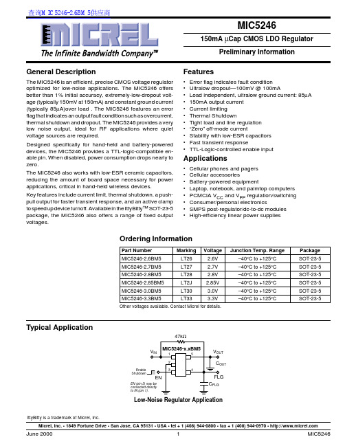
General DescriptionThe MIC5246 is an efficient, precise CMOS voltage regulator optimized for low-noise applications. The MIC5246 offers better than 1% initial accuracy, extremely-low-dropout volt-age (typically 150mV at 150mA) and constant ground current (typically 85µA)over load . The MIC5246 features an error flag that indicates an output fault condition such as overcurrent, thermal shutdown and dropout. The MIC5246 provides a very low noise output, ideal for RF applications where quiet voltage sources are required.Designed specifically for hand-held and battery-powered devices, the MIC5246 provides a TTL-logic-compatible en-able pin. When disabled, power consumption drops nearly to zero.The MIC5246 also works with low-ESR ceramic capacitors, reducing the amount of board space necessary for power applications, critical in hand-held wireless devices.Key features include current limit, thermal shutdown, a push-pull output for faster transient response, and an active clamp to speed up device turnoff. Available in the IttyBitty™ SOT-23-5 package, the MIC5246 also offers a range of fixed output voltages.Features•Error flag indicates fault condition•Ultralow dropout—100mV @ 100mA•Load independent, ultralow ground current: 85µA •150mA output current•Current limiting•Thermal Shutdown•Tight load and line regulation•“Zero” off-mode current•Stability with low-ESR capacitors•Fast transient response•TTL-Logic-controlled enable input Applications•Cellular phones and pagers•Cellular accessories•Battery-powered equipment•Laptop, notebook, and palmtop computers •PCMCIA V CC and V PP regulation/switching •Consumer/personal electronics•SMPS post-regulator/dc-to-dc modules•High-efficiency linear power suppliesOrdering InformationMicrel, Inc. • 1849 Fortune Drive • San Jose, CA 95131 • USA • tel + 1 (408) 944-0800 • fax + 1 (408) 944-0970 • MIC5246Micrel Pin ConfigurationMIC5246-x.xBM5Absolute Maximum Ratings (Note 1)Supply Input Voltage (V IN)..................................0V to +7V Enable Input Voltage (V EN)..................................0V to V IN Flag Output Voltage (V FLG)..................................0V to V IN Junction Temperature (T J)......................................+150°C Storage Temperature...............................–65°C to +150°C Lead Temperature (soldering, 5 sec.).......................260°C ESD, Note 3Operating Ratings (Note 2)Input Voltage (V IN).........................................+2.7V to +6V Enable Input Voltage (V EN)..................................0V to V IN Flag Output Voltage (V FLG)..................................0V to V IN Junction Temperature (T J).......................–40°C to +125°C Thermal Resistance (θJA)......................................235°C/WPin DescriptionPin Number Pin Name Pin Function1IN Supply Input2GND Ground3EN Enable/Shutdown (Input): CMOS compatible input. Logic high = enable;logic low = shutdown. Do not leave open.4FLG Error Flag (Output): Open-drain output. Active low indicates an outputundervoltage condition.5OUT Regulator OutputMIC5246Micrel Electrical CharacteristicsV IN = V OUT + 1V, V EN = V IN; I OUT = 100µA; T J = 25°C, bold values indicate –40°C ≤ T J≤ +125°C; unless noted.Symbol Parameter Conditions Min Typical Max Units V O Output Voltage Accuracy I OUT = 0mA–11%–22%∆V LNR Line Regulation V IN = V OUT + 0.1V to 6V–0.300.3%/V ∆V LDR Load Regulation I OUT = 0.1mA to 150mA, Note 423% V IN– V OUT Dropout Voltage, Note 5I OUT = 100µA 1.55mVI OUT = 50mA5085mVI OUT = 100mA100150mVI OUT = 150mA150200mV250mV I Q Quiescent Current V EN≤ 0.4V (shutdown)0.21µA I GND Ground Pin Current, Note 6I OUT = 0mA85150µAI OUT = 150mA85150µA PSRR Power Supply Rejection f = 120Hz, C OUT = 10µF50dB I LIM Current Limit V OUT = 0V160300mA Enable InputV IL Enable Input Logic-Low Voltage V IN = 2.7V to 5.5V, regulator shutdown0.80.4VV IH Enable Input Logic-High Voltage V IN = 2.7V to 5.5V, regulator enabled 1.61VI EN Enable Input Current V IL≤ 0.4V0.01µAV IH≥ 1.6V0.01µA Shutdown Resistance Discharge500ΩThermal ProtectionThermal Shutdown Temperature150°CThermal Shutdown Hysteresis10°C Error FlagV FLG Low Threshold% of V OUT (Flag ON)90% High Threshold% of V OUT (Flag OFF)96%V OL Output Logic-Low Voltage I L = 100µA, fault condition0.020.4VI FL Flag Leakage Current flag off, V FLG = 6V0.01µANote 1.Exceeding the absolute maximum rating may damage the device.Note 2.The device is not guaranteed to function outside its operating rating.Note 3.Devices are ESD sensitive. Handling precautions recommended.Note 4.Regulation is measured at constant junction temperature using low duty cycle pulse testing. Parts are tested for load regulation in the load range from 0.1mA to 150mA. Changes in output voltage due to heating effects are covered by the thermal regulation specification.Note 5.Dropout voltage is defined as the input to output differential at which the output voltage drops 2% below its nominal value measured at 1V differential. For outputs below 2.7V, dropout voltage is the input-to-output voltage differential with the minimum input voltage 2.7V. Minimum input operating voltage is 2.7V.Note 6.Ground pin current is the regulator quiescent current. The total current drawn from the supply is the sum of the load current plus the ground pin current.Note 7.The error flag is a function of the output voltage being 5% low and the detection of one of the following: overcurrent, overtemperature or dropout. See “Applications Information” section for additional information.MIC5246Micrel1x 101x 101x 101x 101x 101x 10P S R R (d B )FREQUENCY (Hz)Power Supply Rejection Ratio1x 101x 101x 101x 101x 101x 10P S R R (d B )FREQUENCY (Hz)Power Supply Rejection Ratio1x 101x 101x 101x 101x 101x 10P S R R (d B )FREQUENCY (Hz)Power Supply Rejection Ratio1x 101x 101x 101x 101x 101x 10P S R R (d B )FREQUENCY (Hz)Power Supply Rejection RatioG R O U N D C U R R E N T(µA )OUTPUT CURRENT (mA)Ground Current vs. Output CurrentG R O U N D C U R R E N T (µA )TEMPERATURE (°C)Ground Pin CurrentG R O U N D C U R R E N T (µA)TEMPERATURE (°C)Ground Pin CurrentG R O U N D C U R R E N T (µA)VOLTAGE IN (V)Ground Pin CurrentG R O U N D C U R R E N T (µA )VOLTAGE IN (V)Ground Pin CurrentV O L T A G E O U T (V )VOLTAGE IN (V)Dropout CharacteristicsD R O P O U T V O L T A GE (µV )TEMPERATURE (°C)Dropout VoltageD R O P O U T V O L T A GE (µV )TEMPERATURE (°C)Dropout VoltageTypical CharacteristicsMIC5246MicrelTypical CharacteristicsS H O R T C I R C U I T C U R R E N T (m A )TEMPERATURE (°C)Short Circuit Current vs. TemperatureO U T P U T V O L T A G E (V )TEMPERATURE (°C)Output Voltage vs. TemperatureMIC5246Micrel Block DiagramsINENOUTFLGMIC5246MicrelApplications InformationEnable/ShutdownThe MIC5246 comes with an active-high enable pin that allows the regulator to be disabled. Forcing the enable pin low disables the regulator and sends it into a “zero” off-mode-current state. In this state, current consumed by the regulator goes nearly to zero. Forcing the enable pin high enables the output voltage. This part is CMOS and the enable pin cannot be left floating; a floating enable pin may cause an indetermi-nate state on the output.Input CapacitorAn input capacitor is not required for stability. A 1µF input capacitor is recommended when the bulk ac supply capaci-tance is more than 10 inches away from the device, or when the supply is a battery.Output CapacitorThe MIC5246 requires an output capacitor for stability. The design requires 1µF or greater on the output to maintain stability. The capacitor can be a low-ESR ceramic chip capacitor. The MIC5246 has been designed to work specifi-cally with the low-cost, small chip capacitors. Tantalum capacitors can also be used for improved capacitance over temperature. The value of the capacitor can be increased without bound.X7R dielectric ceramic capacitors are recommended be-cause of their temperature performance. X7R-type capaci-tors change capacitance by 15% over their operating tem-perature range and are the most stable type of ceramic capacitors. Z5U and Y5V dielectric capacitors change value by as much 50% and 60% respectively over their operating temperature ranges. To use a ceramic chip capacitor with Y5V dielectric, the value must be much higher than an X7R ceramic or a tantalum capacitor to ensure the same minimum capacitance value over the operating temperature range. Tantalum capacitors have a very stable dielectric (10% over their operating temperature range) and can also be used with this device.Error FlagThe error flag output is an active-low, open-drain output that drives low when a fault condition AND an undervoltage detection occurs. Internal circuitry intelligently monitors overcurrent, overtemperature and dropout conditions and ORs these outputs together to indicate some fault condition. The output of that OR gate is ANDed with an output voltage monitor that detects an undervoltage condition. That output drives the open-drain transistor to indicate a fault. This prevents chattering or inadvertent triggering of the error flag. The error flag must be pulled up using a resistor from the flag pin to either the input or the output.Error Flag CircuitThe error flag circuit was designed essentially to work with a capacitor to ground to act as a power-on reset generator, signaling a power-good situation once the regulated voltage was up and/or out of a fault condition. This capacitor delays the error signal from pulling high, allowing the downstream circuits time to stabilize. When the error flag is pulled up to the input without using a pull-down capacitor, then there can be a glitch on the error flag upon start up of the device. This is due to the response time of the error flag circuit as the device starts up. When the device comes out of the zero off mode current state, all the various nodes of the circuit power up before the device begins supplying full current to the output capacitor. The error flag drives low immediately and then releases after a few microseconds. The intelligent circuit that triggers an error detects the output going into current limit AND the output being low while charging the output capacitor. The error output then pulls low for the duration of the turn-on time. This glitch is filtered by putting a capacitor from the error flag to ground. The glitch does not occur if the error flag pulled up to the output.Transient ResponseThe MIC5246 implements a unique output stage to dramati-cally improve transient response recovery time. The output is a totem-pole configuration with a P-channel MOSFET pass device and an N-channel MOSFET clamp. The N-channel clamp is a significantly smaller device that prevents the output voltage from overshooting when a heavy load is removed. This feature helps to speed up the transient re-sponse by significantly decreasing transient response recov-ery time during the transition from heavy load (100mA) to light load (85µA).Active ShutdownThe MIC5246 also features an active shutdown clamp, which is an N-channel MOSFET that turns on when the device is disabled. This allows the output capacitor and load to dis-charge, de-energizing the load.Thermal ConsiderationsThe MIC5246 is designed to provide 150mA of continuous current in a very small package. Maximum power dissipation can be calculated based on the output current and the voltage drop across the part. To determine the maximum power dissipation of the package, use the junction-to-ambient ther-mal resistance of the device and the following basic equation: PT TD(max)J(max)AJA=−θT J(max) is the maximum junction temperature of the die, 125°C, and T A is the ambient operating temperature. θJA is layout dependent; Table 1 shows examples of junction-to-ambient thermal resistance for the MIC5246.PackageθJA RecommendedθJA 1" SquareθJCMinimum Footprint Copper CladSOT-23-5 (M5)235°C/W185°C/W145°C/W Table 1.SOT-23-5 Thermal ResistanceMIC5246Micrel The actual power dissipation of the regulator circuit can bedetermined using the equation:P D = (V IN– V OUT) I OUT + V IN I GNDSubstituting P D(max) for P D and solving for the operatingconditions that are critical to the application will give themaximum operating conditions for the regulator circuit. Forexample, when operating the MIC5246-3.0BM5 at 50°C witha minimum footprint layout, the maximum input voltage for aset output current can be determined as follows:P 125C5C 235C/WD(max)=°−°°P D(max) = 315mWThe junction-to-ambient thermal resistance for the minimum footprint is 235°C/W, from Table 1. The maximum power dissipation must not be exceeded for proper operation. Using the output voltage of 3.0V and an output current of 150mA, the maximum input voltage can be determined. Because this device is CMOS and the ground current is typically 100µA over the load range, the power dissipation contributed by the ground current is < 1% and can be ignored for this calculation.315mW = (V IN– 3.0V)150mA315mW = V IN·150mA – 450mW810mW = V IN·150mAV IN(max) = 5.4VTherefore, a 3.0V application at 150mA of output current can accept a maximum input voltage of 5.4V in a SOT-23-5 package. For a full discussion of heat sinking and thermal effects on voltage regulators, refer to the Regulator Thermals section of Micrel’s Designing with Low-Dropout Voltage Regu-lators handbook.Fixed Regulator ApplicationsFFigure 1. Low-Noise Fixed Voltage Application Figure 1 shows a standard low-noise configuration with a 47kΩ pull-up resistor from the error flag to the input voltage and a pull-down capacitor to ground for the purpose of fault indication.Dual-Supply OperationWhen used in dual supply systems where the regulator load is returned to a negative supply, the output voltage must be diode clamped to ground.MIC5246Micrel Package InformationSOT-23-5 (M)MIC5246MicrelMIC5246Micrel June 200011MIC5246MIC5246MicrelMICREL INC.1849 FORTUNE DRIVE SAN JOSE, CA95131USATEL + 1 (408) 944-0800 FAX + 1 (408) 944-0970 WEB This information is believed to be accurate and reliable, however no responsibility is assumed by Micrel for its use nor for any infringement of patents or other rights of third parties resulting from its use. No license is granted by implication or otherwise under any patent or patent right of Micrel Inc.© 2000 Micrel IncorporatedMIC524612June 2000。
RA心形指向性动圈式麦克风汇总
RA心形指向性动圈式麦克风汇总心形指向性动圈式麦克风是一种常见的麦克风类型,它具有指向性的特点,可以减少周围环境声音的干扰并提高声音的清晰度。
心形指向性动圈式麦克风广泛应用于舞台演出、录音室、会议室等场合,下面将对几款常见的心形指向性动圈式麦克风进行汇总。
首先是Shure SM58,它是一款经典的心形指向性动圈式麦克风。
SM58具有出色的声音传输能力和抗反馈特性,在舞台表演和音乐录制方面广泛应用。
它采用了动圈式麦克风的设计,能够有效地减少周围环境的噪音,提供清晰、生动的声音。
此外,SM58还具有耐用性和可靠性,经受得住长时间使用和频繁的移动。
另一款值得一提的心形指向性动圈式麦克风是Audio-Technica ATR2100x。
ATR2100x是一款多功能的麦克风,可用于电脑录音、现场演出和家庭录音等多种场合。
它具有动圈式麦克风的特点,可减少周围环境噪音的干扰。
此外,ATR2100x还具有USB接口和XLR接口,可以直接连接到电脑或其他录音设备进行录音。
它还配备了耳机监控功能,可以实时监听录音效果。
再来说说Sennheiser E835,它是一款专业级的心形指向性动圈式麦克风。
E835采用了Sennheiser的专利技术,具有高质量的声音传输和准确的指向性表现。
它适用于现场演出、录音室和广播等各种场合。
E835不仅声音质量出色,而且具有高度的抗噪能力和抗反馈能力,可以有效地减少背景噪音和意外噪音的干扰。
最后一个要提到的是AKGD5,它是一款专业级的心形指向性动圈式麦克风。
D5采用了AKG的专有技术,具有出色的声音传输和音质表现。
它可以提供清晰、明亮的声音,并具有高度的抗反馈能力。
AKGD5适用于各种现场演出和录音场合,同时也是一款非常耐用的麦克风,可以承受长时间的使用和频繁的移动。
总结起来,心形指向性动圈式麦克风是一种广泛应用于音乐表演、录音等场合的麦克风类型。
以上介绍了几款常见的心形指向性动圈式麦克风,它们分别是Shure SM58、Audio-Technica ATR2100x、Sennheiser E835和AKG D5、无论是在舞台演出、录音室还是会议室中,这些麦克风都能够提供清晰、生动的声音,并减少周围环境的噪音干扰。
MIC5236
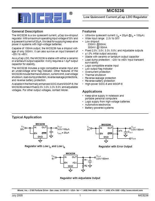
Micrel, Inc.
MIC5236
Low Quiescent Current µCap LDO Regulator
General Description
The MIC5236 is a low quiescent current, µCap low-dropout regulator. With a maximum operating input voltage of 30V and a quiescent current of 20µA, it is ideal for supplying keep-alive power in systems with high-voltage batteries. Capable of 150mA output, the MIC5236 has a dropout voltage of only 300mV. It can also survive an input transient of –20V to +60V. As a µCap LDO, the MIC5236 is stable with either a ceramic or a tantalum output capacitor. It only requires a 1.0µF output capacitor for stability. The MIC5236 includes a logic compatible enable input and an undervoltage error flag indicator. Other features of the MIC5236 include thermal shutdown, current-limit, overvoltage shutdown, load-dump protection, reverse leakage protections, and reverse battery protection. Available in the thermally enhanced SOIC-8 and MSOP-8, the MIC5236 comes in fixed 2.5V, 3.0V, 3.3V, 5.0V, and adjustable voltages. For other output voltages, contact Micrel.
MiCOM Labs 2.4 GHz RF 模块说明书

Certificate of Radio Equipment in JapanMiCOM Labs Inc operating as Recognized Conformity Assessment Body (RCB ID Number: 210) with respect to Japan, declares that the listed product complies with the Technical Regulations Conformity Certification of Specified Radio equipment (ordinance of MPT N° 37, 1981)Applicant Name: Digi InternationalApplicant Address: 355 South 520 West, Suite 180 Lindon, Utah, 84042 USAModel Name: S6BSMProduct description: 2.4 GHz RF Module Classification of specifiedradio equipment:Article 2, Paragraph 1, Item 19Frequency Band ModeEmissionDesignatorPowermW/MHzType of Emissions Frequency and Antenna power 2412-2472 MHz 802.11b 14M5GXW 7.0 mW/MHz 2412-2472 MHz 802.11g 18M5DXW 4.0 mW/MHz 2412-2472 MHz 802.11n 19M0DXW 3.3 mW/MHzFrequency Allocation (GHz) 2412, 2417, 2422, 2427, 2432, 2437, 2442, 2447, 2452,2457, 2462, 2467, 2472 MHzHardware / Software revision 02 REV A / 1200xCertification number R210-101057This is to certify that the above mentioned certification by type has been granted in accordance with the provisions of Article 38-24, Paragraph 1 of the Radio Law.Name: Gordon HurstTitle: Certification ManagerAddress: MiCOM Labs Inc, Pleasanton, CA [Note: This certificate has THREE Annexes]Annex 1 to certificate of Radio Equipment in JapanCertificate Number; R210-101057The validity of this Certificate is limited to products, which are equal to the one examined in the type-examination.• When the manufacturer (or holder of this certificate) is placing the product on the Japanese market, the product must be affixed with the following Specified Radio Equipment marking:Remarks and observationsThe following conditions are applicable: Declared Supply voltage: 3.3VDCAntennasModel Type Manufacturer Gain (dBi)Frequency Range (GHz)31000005-01 Internal PCBAntennaDigi International 0 2.4 to 2.5AN2400-37A19BXDipole BEC 2.76 2.4 to 2.5 R-AN2400-5701RS-ZDipole BEC 3.45 2.4 to 2.5-- Integral Whip ¼wave monopoleDIGI International 1.82.4 to 2.5 S131AH-2450S Dipole Nearson 2 2.4 to 2.5 W1030 Dipole Pulse 2 2.4 to 2.5 W1049B050 Dipole Pulse 2 2.4 to 2.5 WLE-HG-DA Directional Buffalo 9 2.4 to 2.5Annex 2 to certificate of Radio Equipment in JapanCertificate Number; R210-101057Documentation lodged for this type-examination:Test Reports:•MiCOM Labs: DIGI30-J4 Rev AProduct Documentation:•Assembly drawings• Layout Drawings•Bill of materials•Block diagram•Electric/Schematic diagrams•Antenna specifications•Photos•User manualTechnical Standards and SpecificationsThe product shows no non-compliances with the following Equipment Radio Regulations (including amendments)- Chapter I, General Provisions- Chapter II, Transmitting Equipment- Chapter III, Receiving Equipment- Chapter IV, section 4.17 article 49.20- Radio equipment specified in Item (19) of article 2, paragraph1.Annex 3 to certificate of Radio Equipment in JapanCertificate Number; R210-101057Technical features and characteristicsThe product includes the following features and characteristics:The XBee® Wi-Fi RF module provides wireless connectivity to end-point devices in 802.11 bgn networks. Using the 802.11 feature set, these modules are interoperable with other 802.11 bgn devices, including devices from other vendors. With XBee, users can have their 802.11 bgn network up-and running in a matter of minutes.The XBee® Wi-Fi modules are compatible with other devices that use 802.11 bgn technologies. These include Digi external 802.11x devices like the ConnectPort products and the Digi Connect Wi-SP, as well as embedded products like the ConnectCore series and Digi Connect series of products. More information on these Digi products can be found at: /products/wireless/wifisolutions/。
MICREL MIC4576 数据手册
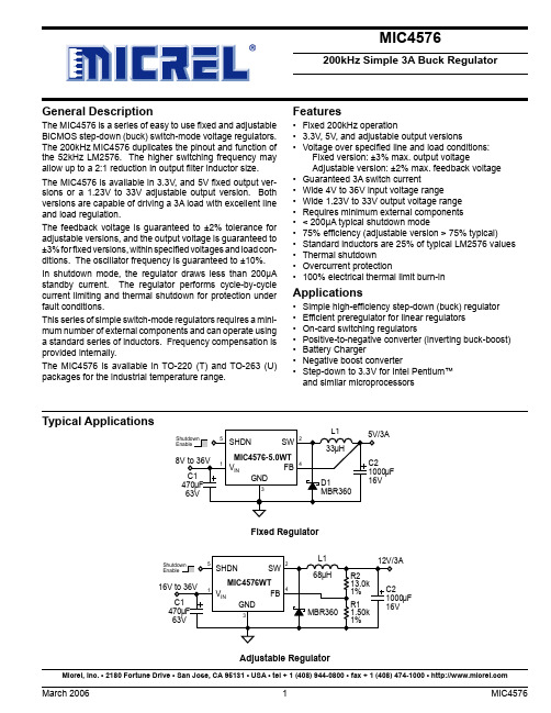
8V ≤ VIN ≤ 36V, 0.5A ≤ ILOAD ≤ 3A
Efficiency Maximum Duty Cycle (On) Output Leakage Current
Quiescent Current Feedback Bias Current
ILOAD = 3A, Note 1 VFB = 1.0V VIN = 36V, VFB = 1.5V output = 0V output = –1V
Micrel, Inc.
Operating Ratings
Supply Voltage (VIN).................................................... +36V Junction Temperature .............................................. +150°C Package Thermal Resistance
In shutdown mode, the regulator draws less than 200µA standby current. The regulator performs cycle-by-cycle current limiting and thermal shutdown for protection under fault conditions.
* RoHS compliant with "high-melting solder" exemption.
Package TO-220-5 TO-220-5 TO-220-5 TO-263-5 TO-263-5 TO-263-5
Pin Configuration
- 1、下载文档前请自行甄别文档内容的完整性,平台不提供额外的编辑、内容补充、找答案等附加服务。
- 2、"仅部分预览"的文档,不可在线预览部分如存在完整性等问题,可反馈申请退款(可完整预览的文档不适用该条件!)。
- 3、如文档侵犯您的权益,请联系客服反馈,我们会尽快为您处理(人工客服工作时间:9:00-18:30)。
MIC5206BMM
Enable (pin 7) may be connected directly to Supply Input (pin 8).
Flag Output (optional)
R2
SOT-23-5 Fixed Voltage Application
Adjustable Voltage Application
Micrel Mini 8™ is a trademark of Micrel, Inc. Micrel, Inc. • 1849 Fortune Drive • San Jose, CA 95131 • USA • tel + 1 (408) 944-0800 • fax + 1 (408) 944-0970 •
For low-dropout regulators that are stable with ceramic output capacitors, see the µCap MIC5245/6/7 family.
Typical Applications
47k VOUT
1 8 7 6 5
VIN
Enable Shutdown
MIC5206
2
January 2000
MIC5206
Micrel
Absolute Maximum Ratings (Note 1)
Supply Input Voltage (VIN) ............................ –20V to +20V Enable Input Voltage (VEN) ........................... –20V to +20V Power Dissipation (PD) ............... Internally Limited, Note 3 Junction Temperature (TJ) ....................... –40°C to +125°C Lead Temperature (Soldering, 5 sec.) ...................... 260°C
January 2000
1
MIC5206
MIC5206
Micrel
Ordering Information
Part Number MIC5206-2.5BM5 MIC5206-2.7BM5 MIC5206-3.0BM5 MIC5206-3.2BM5 MIC5206-3.3BM5 MIC5206-3.6BM5 MIC5206-3.8BM5 MIC5206-4.0BM5 MIC5206-5.0BM5 MIC5206BMM MIC5206-3.0BMM MIC5206-3.3BMM MIC5206-3.6BMM MIC5206-3.8BMM MIC5206-4.0BMM MIC5206-5.0BMM Marking LD25 LD27 LD30 LD32 LD33 LD36 LD38 LD40 LD50 — — — — — — — Volts 2.5 2.7 3.0 3.2 3.3 3.6 3.8 4.0 5.0 Adj 3.0 3.3 3.6 3.8 4.0 5.0 Accuracy 1% 1% 1% 1% 1% 1% 1% 1% 1% 1% 1% 1% 1% 1% 1% 1% Junction Temp. Range –40°C to +125°C –40°C to +125°C –40°C to +125°C –40°C to +125°C –40°C to +125°C –40°C to +125°C –40°C to +125°C –40°C to +125°C –40°C to +125°C –40°C to +125°C –40°C to +125°C –40°C to +125°C –40°C to +125°C –40°C to +125°C –40°C to +125°C –40°C to +125°C Package SOT-23-5 SOT-23-5 SOT-23-5 SOT-23-5 SOT-23-5 SOT-23-5 SOT-23-5 SOT-23-5 SOT-23-5 8-lead MSOP 8-lead MSOP 8-lead MSOP 8-lead MSOP 8-lead MSOP 8-lead MSOP 8-lead MSOP
Applications
• • • • • • • Cellular telephones Laptop, notebook, and palmtop computers Battery-powered equipment PCMCIA VCC and VPP regulation/switching Consumer/personal electronics SMPS post-regulator/dc-to-dc modules High-efficiency linear power supplies
MIC5206-x.xBMM (Fixed Output Voltage)
MIC5206BMM (Adjustable Ouput Voltage)
Pin Description
MIC5206 SOT-23-5 1 2 3 4 MIC5206 MSOP-8 8 4, 6 7 3 5 (fixed) 5 (adj.) 5 1,2 Pin Name IN GND EN FLAG BYP ADJ OUT Pin Function Supply Input Ground Enable/Shutdown (Input): CMOS compatible input. Logic high = enable, logic low or open = shutdown. Do not leave floating. Error Flag (Output): Open-collector output. Active low indicates an ouput undervoltage condition. Reference Bypass: Connect external 470pF capacitor to GND to reduce output noise. May be left open. Adjust (Input): Adjustable regulator feedback input. Connect to resistor voltage divider. Regulator Output
Features
• • • • • • • • • • • • Error flag indicates undervoltage fault High output voltage accuracy Guaranteed 150mA output Ultra-low-noise output (8-lead versions) Low quiescent current Low dropout voltage Extremely tight load and line regulation Very low temperature coefficient Current and thermal limiting Reversed-battery protection “Zero” off-mode current Logic-controlled electronic enable
Operating Ratings (Note 2)
Supply Input Voltage (VIN) ........................... +2.5V to +16V Enable Input Voltage (VEN) .................................. 0V to VIN Junction Temperature (TJ) ....................... –40°C to +125°C SOT-23-5 (θJA) ......................................................... Note 3 8-lead MSOP (θJA) ................................................... Note 3
Other voltages available. Contact Micrel for details.
Pin Configuration
EN GND IN
3 2 1
LDxx
4 5
FLAG
OUT
MIC5206-xxBM5 (Fixed Output Voltage)
OUT OUT FLAG GND 1 2 3 4 8 7 6 5 IN EN GND BYP OUT OUT FLAG GND 1 2 3 4 8 7 6 5 IN EN GND ADJ
MIC5206-x.xBM5 VIN
1 2 Enable Shutdown Enable (pin 3) may be connected directly to Supply Input (pin 1). 3 4 5
1µF
2 3 4
VOUT 100k COUT 1µF tantalum
Flag Output (optional) tantalum R1
MIC5206
Micrel
MIC5206
150mA Low-Noise LDO Regulator
General Description
The MIC5206 is an efficient linear voltage regulator with very low dropout voltage (typically 17mV at light loads and 165mV at 150mA), and very low ground current (600µA at 100mA output), with better than 1% initial accuracy. It has a logic compatible enable/shutdown control input and an internal undervoltage monitor. Designed especially for hand-held, battery-powered devices, the MIC5206 can be switched by a CMOS or TTL compatible logic signal. When disabled, power consumption drops nearly to zero. Dropout ground current is minimized to prolong battery life. Key features include an undervoltage monitor with an error flag output, a reference bypass pin to improve its already lownoise performance (8-lead versions only), reversed-battery protection, current limiting, and overtemperature shutdown. The MIC5206 is available in several fixed voltages in a tiny SOT-23-5 package. It features a pinout, similar to the LP2980, but has significantly better performance. Fixed and adjustable output voltage versions, featuring the reference bypass option, are available in the 8-lead Micrel Mini 8™ 8-lead MSOP (micro small-outline package).
