LANC122.5W12-S中文资料
5000UP音频线双导体12AWGBC未屏蔽CL3商业音频线规格参数介绍及应用场景说明书

1,000 ft 612825154686
5000UP 009U500 White
UnReel
500 ft 612825154747
5000UP 0091000 White
Reel
1,000 ft 612825154716
© 2022 Belden, Inc
All Rights Reserved.
Although Belden makes every reasonable effort to ensure their accuracy at the time of this publication, information and specifications described here in are subject to error or omission and to change without notice, and the listing of such information and specifications does not ensure product availability.
26 Amps per conductor @ 25°C
Voltage UL Voltage Rating 300 V (CL3)
Mechanical Characteristics
Temperature
UL Temperature Operating
75°C
end Radius Stationary Min. Installation Min. 3.1 in (79 mm) 3.1 in (79 mm)
Electrical Characteristics
Electricals
Element
LANC482.5W12中文资料
元器件交易网
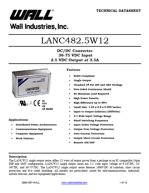
TECHNICAL DATASHEET
LANC482.5W12
Technical Specifications
All specifications are based on 25 oC, Nominal Input Voltage and Maximum Output Current unless otherwise noted. We reserve the right to change specifications based on technological advances. SPECIFICATION Related condition Min Nom Max Unit Switching Frequency Test at nominal Vin and full load 400 kHz INPUT (Vin) Operating Voltage Range 36 48 75 Vdc Input Voltage (Continuous) 80 Vdc Input Voltage (Transient 100ms) 100 Vdc UVLO Turn-on Threshold 36 Vdc UVLO Turn-off Threshold 33 Vdc Input Standby Current Nominal Vin and No Load 10 mA Input Voltage Variation Complies with EST300 132 part 4.4 5 V/ms Input Current Nominal Vin and Full Load 231 mA 5 to 20MHz, 12µH source impedance Reflected Ripple Current 20 mApk-pk (See the Test Setup section - pg 8) Test at nominal Vin and full load 83 % EFFICIENCY (See the Test Setup section – pg 8) OUTPUT (Vo) Operating Output Range Nominal Vin and Full Load 2.47 2.5 2.53 Vdc Load Regulation 0% to 100% Full Load -1.0 +1.0 % Line Regulation LL to HL at Full Load -0.2 +0.2 % 5Hz to 20MHz bandwidth Output Ripple & Noise 85 mVpk-pk (See the Test Setup section - pg 8) Output Current 0 3.5 A Output Voltage Overshoot LL to HL at Full Load 0 3 % Vout Over Voltage Protection Zener diode clamp 3.9 Vdc Over Current Protection 150 % FL Short Circuit Protection Continuous, automatic recovery Test at nominal Vin DYNAMIC LOAD RESPONSE Peak Deviation Load step change from 75 to 100% or 100 to 75 % of FL 200 mV Setting Time (Vout < 10% peak deviation) 250 µs The ON/OFF pin voltage is referenced to -Vin REMOTE ON/OFF (See the Remote ON/OFF Control section - pg 5) ON/OFF pin High Voltage (Remote ON) 3.0 12 Vdc ON/OFF pin Low Voltage (Remote OFF) 0 1.2 Vdc ON/OFF pin Low Voltage, input current 2.5 mA Test at nominal Vin and constant resistive load START UP TIME Power Up 450 ms Remote ON/OFF 5 ms ISOLATION Isolation Voltage (Input-Output) 1600 Vdc Isolation Voltage (Output to Case–DIP Type) 1600 Vdc Isolation Voltage (Output to Case–SMT Type) 1000 Vdc Isolation Voltage (Input to Case - DIP Type) 1600 Vdc Isolation Voltage (Input to Case - SMT Type) 1000 Vdc Isolation Resistance 1 GΩ Isolation Capacitance 1200 pF ENVIRONMENTAL o Operating Ambient Temperature (w/ derating) -40 85 C o Operating Case Temperature 100 C o Storage Temperature -55 105 C Temperature Coefficient -0.02 +0.02 % / oC See the MTBF and Reliability section (pg 13) MTBF Bellcore TR-NWT-000332, TC=40°C 2,750,000 hours MIL-STD-217F 1,080,000 hours MECHANICAL See Figure 1 Weight 18.0 grams Dimensions 1.25 x 0.8 x 0.450 inches
宝马宝·R12 电视机说明书

lockable cabinet capable of housing up to 7 AH batter-
ies.
OPTIONAL REMOTE ANNUNCIATOR
The RZA-5F is a five-zone Remote Annunciator for use with the FireWatch 5000 Series control/communicators. They mount to a single-gang box and offer slide-in zone identification labels. The RZA-5F provides the following:
Initiating Device Circuits (zones)
The MS-5012 includes five programmable Initiating Device Circuits (zones). Circuits 1, 2, 4, and 5 are Style B (Class B). Circuit 3 is Style D (Class A).
DF-51186 07/12/04 Page 1 of 3
SPECIFICATIONS
Single PC board design using Surface Mount Technology (SMT).
Two modular telephone jacks for connection to RJ31X/ Modules.
16-Event history buffer.
MS-5012
Accurate real-time clock.
Extensive built-in transient protection.
LANC2412UW8中文资料
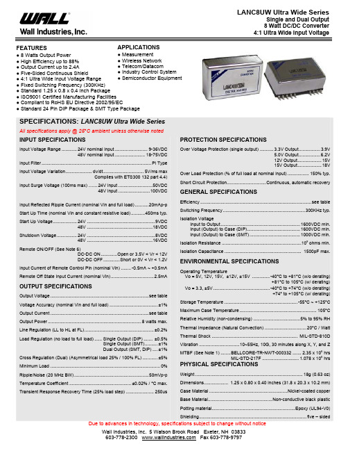
FEATURES● 8 Watts Output Power● High Efficiency up to 88%● Output Current up to 2.4A● Five-Sided Continuous Shield● 4:1 Ultra Wide Input Voltage Range● Fixed Switching Frequency (300KHz) ● Standard 1.25 x 0.8 x 0.4 Inch Package ● ISO9001 Certified Manufacturing Facilities ● Compliant to RoHS EU Directive 2002/95/EC● Standard 24 Pin DIP Package & SMT Type PackageSPECIFICATIONS: LANC8UW Ultra Wide SeriesAll specifications apply @ 25°C ambient unless otherwise notedINPUT SPECIFICATIONSInput Voltage Range............24V nominal input..........................9-36VDC 48V nominal input........................18-75VDCInput Filter.......................................................................................Pi TypeInput Voltage Variation.....................dv/dt................................5V/ms maxComplies with ETS300 132 part 4.4)Input Surge Voltage (100ms max) …… 24V input ...........................50VDC 48V input .........................100VDCInput Reflected Ripple Current (nominal Vin and full load)...........20mAp-pStart Up Time (nominal Vin and constant resistive load)...........450ms typ.Start Up Voltage...................24V ......................................................9VDC48V ....................................................18VDCShutdown Voltage................24V ......................................................8VDC48V ....................................................16VDCRemote ON/OFF (See Note 6)DC-DC ON.............Open or 3.5V < Vr < 12V DC-DC OFF.............Short or 0V < Vr < 1.2VInput Current of Remote Control Pin (nominal Vin)........-0.5mA ~ +0.5mARemote Off State Input Current (nominal Vin)..................................2.5mAOUTPUT SPECIFICATIONSOutput Voltage..............................................................................see tableVoltage Accuracy (nominal Vin and full load) (1)Output Current..............................................................................see tableOutput Power..........................................................................8 watts max.Line Regulation (LL to HL at FL).......................................................±0.2%Load Regulation (no load to full load)......Single Output (DIP)....... ±0.5%Single Output (SMT)..........±1% Dual Output (SMT, DIP). (1)Cross Regulation (Dual) (Asymmetrical load 25% / 100% FL) (5)Minimum Load .......................................................................................0%Ripple/Noise (20 MHz BW)...........................................................50mVp-pTemperature Coefficient .................................................±0.02% / °C max.Transient Response Recovery Time (25% load step)......................250usPROTECTION SPECIFICATIONSOver Voltage Protection (single output)...........3.3V Output.................3.9V5.0V Output.................6.2V 12V Output...................15V 15V Output. (18V)Over Load Protection (% of full load at nominal input).................150% typ.Short Circuit Protection...............................Continuous, automatic recoveryGENERAL SPECIFICATIONS Efficiency........................................................................................see tableSwitching Frequency.................................................................300KHz typ.Isolation VoltageInput to Output...............................................................1600VDC min.Input (Output) to Case (DIP)..........................................1600VDC min. Input (Output) to Case (SMT)........................................1000VDC min.Isolation Resistance (109)ohms min.Isolation Capacitance............................................................. 1500pF max.ENVIRONMENTAL SPECIFICATIONSOperating TemperatureVo = 5V, 12V, 15V, ±12V, ±15V ..............-40°C to +81°C (w/o derating) +81°C to 105°C (w/ derating)Vo = 3.3, ±5V.............................................-40°C to +74°C (w/o derating) +74° to +105°C (w/ derating)Storage Temperature ..........................................................-55°C ~ +125°CMaximum Case Temperature.............................................................105°CRelative Humidity (non-condensing).....................................5% to 95% RHThermal Impedance (Natural Convection).................................20°C / WattThermal Shock .................................................................... MIL-STD-810DVibration ................................10~55Hz, 10G, 30 minutes along X, Y, and ZMTBF (See Note 1)........BELLCORE-TR-NWT-000332.......2.35 x 106hrsMIL-STD-217F .............................1.078 x 106hrsPHYSICAL SPECIFICATIONSWeight .....................................................................................18g (0.63 oz)Dimensions................... 1.25 x 0.80 x 0.40 inches (31.8 x 20.3 x 10.2 mm)Case Material ..............................................................Nickel-coated copperBase Material...................................................Non-conductive black plasticPotting material..................................................................Epoxy (UL94-V0)Shielding.....................................................................................five – sidedDue to advances in technology, specifications subject to change without noticeAPPLICATIONS● Measurement ● Wireless Network ● Telecom/Datacom ● Industry Control System ● Semiconductor EquipmentSAFETY & EMCApprovals and Standards.................IEC60950-1, UL60950-1, EN60950-1EMI (See Note 7)...............EN55022.............................................Class AESD....................EN61000-4-2…….. ……Perf. Criteria B Radiated Immunity...........EN61000-4-3……………10V/m Perf. Criteria AFast Transient..................EN61000-4-4...................±2KV Perf. Criteria BSurge (See Note 8)..........EN61000-4-5……………..±1KV Perf. Criteria BConducted Immunity…… EN61000-4-6……….…10 Vrms Perf. Criteria AOUTPUT VOLTAGE / CURRENT RATING CHARTOutput Current Input Current Model NumberInput RangeOutput Voltage Min. load Full load Output (2) Ripple & Noise No load (3) Full load (2) Efficiency (4)Capacitor(5)Load maxLANC2433UW8 3.3 VDC 0mA 2400mA 50mVp-p 40mA 407mA 85% 1330uF LANC2405UW8 5 VDC 0mA 1600mA 50mVp-p 40mA 402mA 87% 1330uFLANC2412UW8 12 VDC 0mA 666mA 50mVp-p 25mA 407mA 86% 288uFLANC2415UW8 15 VDC 0mA 533mA 50mVp-p 25mA 407mA 86% 200uF LANC2405DUW8 ±5 VDC 0mA ±800mA 50mVp-p 20mA 417mA 84% ±900uF LANC2412DUW8 ±12 VDC 0mA ±333mA 50mVp-p 25mA 407mA 86% ±133uFLANC2415DUW824VDC (9 - 36 VDC)±15 VDC 0mA ±267mA 50mVp-p 25mA 407mA 86% ±90uF LANC4833UW8 3.3 VDC 0mA 2400mA 50mVp-p 20mA 204mA 85% 1330uF LANC4805UW8 5 VDC 0mA 1600mA 50mVp-p 20mA 201mA 87% 1330uFLANC4812UW8 12 VDC 0mA 666mA 50mVp-p 13mA 201mA 87% 288uFLANC4815UW8 15 VDC 0mA 533mA 50mVp-p 13mA 198mA 88% 200uF LANC4805DUW8 ±5 VDC 0mA ±800mA 50mVp-p 10mA 208mA 84% ±900uF LANC4812DUW8 ±12 VDC 0mA ±333mA 50mVp-p 13mA 201mA 87% ±133uF LANC4815DUW8 48VDC (18 - 75 VDC) ±15 VDC 0mA ±267mA 50mVp-p 13mA 201mA 87% ±90uFNOTES1.BELLCORE TR-NWT-000332. Case I: 50% Stress, Temperature at 40ºC. (Ground fixed and controlled environment) MIL-STD-217F Notice2 @Ta=25 ºC, Full load (Ground, Benign, controlled environment) 2. Maximum value at nominal input voltage and full load. 3. Typical value at nominal input voltage and no load. 4. Typical value at nominal input voltage and full load. 5. Test by minimum Vin and constant resistive load. 6. The ON/OFF control pin voltage is referenced to -Vin.7. The LANC8UW Series can meet EN55022 Class A with an external capacitor in parallel with the input pins.Recommend: 24Vin: 1µF/50V48Vin: 0.47µF/100V8. An external filter capacitor is required if the module has to meet EN61000-4-5. The filter capacitor Wall Industries suggests: Nippon chemi-con KY Series, 220uF/100V, ESR 48m Ω.Air ± 8KV Contact ± 6KVMECHANICAL DRAWING(DIP) PIN CONNECTIONPIN SINGLE DUAL PIN SINGLE DUAL 1 CTRL CTRL 2 -INPUT -INPUT 23 +INPUT +INPUT 3 -INPUT -INPUT 22 +INPUT +INPUT 9 NC COMMON 16 -OUTPUTCOMMON 11 NC -OUTPUT 14 +OUTPUT +OUTPUTRecommended Filter for EN55022 Class B ComplianceLoadRecommended EN55022 Class B Filter Circuit LayoutThe components used in the Figure 1, together with the manufacturers’ part numbers for these components, are as follows:C1 C2 C3C4L1 LANC24xxUW8 4.7uF/50V N/A1000pF/2KV 1000pF/2KV325uH Common Choke LANC48xxUW8 1.5uF/100V 1.5uF/100V 1000pF/2KV 1000pF/2KV325uH Common ChokeFIGURE 1FIGURE 2(SMT) PIN CONNECTIONPIN SINGLE DUAL PIN SINGLE DUAL1 CTRL CTRL2 -INPUT -INPUT 23 +INPUT +INPUT 3 -INPUT -INPUT 22 +INPUT +INPUT 9 NC COMMON 16 -OUTPUT COMMON 11 NC -OUTPUT 14 +OUTPUT +OUTPUT Others NC NC Others NC NC1. All dimensions are in inches (mm) Tolerance: X.XX±0.02 (X.X±0.5) X.XXX±0.01 (X.XX±0.25)2. Pin pitch tolerance ±0.01 (0.25)LANC8UWSERIES。
美国邦纳工业照明灯及工业智能指示灯
目录
点亮工厂......................................................................................................... 4
邦纳照明灯及指示灯解决方案 LED 照明灯..............................................................................................14 节能耐用,设计美观的LED照明灯产品适用于多种工业及移动环境 信号塔灯.................................................................................................. 30 信号塔灯采用优质LED,外观时尚,并有多种便于安装的附件可供选择 指示灯..................................................................................................... 40 指示灯产品坚固耐用,无需另外的保护外壳,独特的设计可为各种指示灯 应用提供多样的尺寸和安装方式 触摸按钮.................................................................................................. 76 邦纳的工业按钮产品同样种类丰富,功能齐全。他们有着耐用的包装,无 需另外的保护外壳 Pick-to-Light系列.................................................................................. 88 设计独特,坚固耐用的Pick-to-Light系列产品能够有效减少装配过程时 间,为操作人员提高工作效率
XC12英文用户指南说明书

MICRO Hi-Fi SYSTEM ] USER GUIDE 3want to play.station sound effect.SLEEP Turn on or offMP3 Info while a file isimpressions. To change the functions, you can scroll throughthem and select one. (see Listening to the CDs)once to repeat the track REPEAT twice to CD. The MICRO Hi-Fi SYSTEM ] USER GUIDE 5MICRO Hi-Fi SYSTEM ] USER GUIDE 7Listen to cassette tapes - more you can doTo Play Fast backward or ForwardAfter pressing bb /BB during playback, or stop, press B at a point you want.Listening to the radio - more you can doLook for radio stations automaticallyPress - TUNING +(o r TUN.- /TUN.+) for more than 0.5 second. The tuner will scan automatically and stop when it finds a radio station.Delete all the saved stationsPress and hold PROGRAM MEMORY or PROGRAM/MEMO for two sec-onds. “CLEAR” shows. Press STOP CLEAR (or x )to erase all the saved stations.Choose a ‘preset number’for a radio stationSelect a station you want by pressing - TUNING +or TUN.- /TUN.+.Press PROGRAM MEMORY or PROGRAM/MEMO ,the station flashes.Press - PRESET +or PRESET/FOLDER to select the preset number you want. Press PROGRAM MEMORY or PROGRAM/MEMO to save it.Improve poor FM receptionPress MODE/RIF on the front panel . This will change the tuner from stereo to mono and usually improve the reception.See information about your radio stations - OPTIONALThe FM tuner is supplied with the Radio Data System (RDS) facility. This shows the letters RDS on the display, plus information about the radio sta-tion being listened to. Press RDS on the front panel several times to view the information.PTY - Programme Type, such as News, Sport, Jazz Music.RT - Radio Text, the name of the radio station.CT - Time Control, the time at the location of the radio station.PS - Programme Service name, the name of channel.You can search the radio stations by programme type by pressing- PRESET +. The display will show the last PTY in use. Press - PRESET +one or more times to select your preferred programme type. Press and hold - TUNING +. The tuner will search automatically. When a station is found the search will stop.MICRO Hi-Fi SYSTEM ] USER GUIDE 9Use your player as an alarm clockPress and hold TIMER for two seconds. Each function, TUNER, CD, USB (in the USB supplied models)flashes for two seconds. Press SET when the function you want to be woken by is showing.If you choose TUNER you will be shown the stations you have saved as presets. Use - TUNING + to select the station you want, then press SET . You will be shown the ON TIME display. This is where you set the time you want the alarm to go off. Use - TUNING +to change the hours and minutes and SET to save.You will then be shown the OFF TIME display. This is where you set the time you want the function to stop. Use - TUNING +to change the hours and minutes and press SET to save.Next you will be shown the volume (VOL) you want to be woken by. Use - TUNING +to change the volume and SET to save. Switch the system off. The clock icon shows that the alarm is set.When the system is turned off you can check the time the alarm is set for by pressing TIMER . You can also turn the alarm on and off by pressing TIMER . To set the alarm to go off at a different time, switch the system on and reprogramme following the same steps as initially.About MP3/WMAMP3/WMA Disc compatibility with this unit is limited as follows:• Sampling Frequency : 8 - 48 kHz (MP3), 32 - 48 kHz (WMA)•Bit rate : 8 - 320 kbps (MP3), 48 - 320 kbps (WMA)• CD-R physical format should be “ISO 9660”• If you record MP3/WMA files using the software which cannot create a FILE SYSTEM, for example “Direct-CD” etc., it is impossible to playback MP3 files. We recommend that you use “Easy-CD Creator”, which creates an ISO 9660 file system.•File names should be named using 30 letters or less and mustincorporate “.mp3”,“.wma” extension e.g. “********.MP3” or “********.WMA”•Do not use special letters such as “/ : * ? “ < >”etc.•Even if the total number of files on the disc has more than 1000, it will only be shown up to 999.MICRO Hi-Fi SYSTEM ] USER GUIDE 11Designs and specifications are subject to change without notice.。
CS1242 用户手册
C S1242用户手册2005年5月目录1CS1242功能说明 (4)1.1 CS1242主要功能特性 (4)1.2 应用场合 (4)1.3 功能描述 (5)2CS1242特性说明 (6)2.1 芯片绝对最大极限值 (6)2.2 CS1242数字逻辑特性 (6)2.3 CS1242的管脚和封装 (7)2.4 CS1242电气特性 (9)2.5 CS1242时序 (11)3CS1242功能模块描述 (13)3.1 输入多路信号选择器(Input Multiplexer) (13)3.2 输入模拟缓冲器(Buffer) (13)3.3 可编程增益放大器(PGA) (13)3.4 调制器(Modulator) (14)3.5 误差校正(Calibration) (14)3.5.1 自校正(Self Calibration) (14)3.5.2 系统校正(System Calibration) (14)3.6 外接参考电压(External Voltage Reference) (14)3.7 时钟单元(Clock Unit) (15)3.8 数字滤波器(FIR) (15)3.9 串行总线接口( SPI ) (16)3.9.1 片选信号( CS ) (16)3.9.2 串行时钟( SCLK ) (16)3.9.3 时钟极性控制( POL ) (16)3.9.4 数据输入( SDI )和数据输出( SDO ) (16)3.10 数据准备就绪 ( DRDY ) (16)3.11 数据同步(SYNC) (16)3.12 上电复位及芯片的复位(RESET) (17)4CS1242寄存器描述 (18)4.1 寄存器列表 (18)4.2 寄存器详细描述 (18)5CS1242指令描述 (23)5.1 CS1242指令列表 (23)5.2 CS1242指令详细描述 (24)6CS1242的封装 (28)图列表图1CS1242原理框图 (5)图2CS1242管脚图 (7)图3CS1242时序图 (11)图4多路输入选择原理框图 (13)图5外部晶振连接图 (15)表清单表1CS1242极限值 (6)表2CS1242数字逻辑特性 (6)表3CS1242管脚描述 (7)表4CS1242封装 (8)表5AVDD=5V时CS1242电气特性 (9)表6AVDD=3V时CS1242电气特性 (10)表7CS1242时序表 (12)表8调制器采样频率表 (14)表9外部参考电压和RAN的关系表 (15)表10内部寄存器详细列表 (18)表11CS1242指令描述表 (23)1CS1242功能说明CS1242是高精度、低功耗模数转换芯片。
上汽大众-全新一代朗逸-使用维护说明书-中文

本说明书适用于下列表中各种型号的上汽大众 All New Lavida 全新一代朗逸系列轿车。
用户在使用本公司产品以前,必须认真研读产品使用维护说明书,任何不当的使用、保养和修理都可能导致车辆的损坏及影响质量担保服务。
因此,在使用产品前请认真阅读本使用维护说明书,并对照表中的型号确认您的车型。
名称型号发动机变速箱全新一代朗逸SVW71221AN DJN七挡自动变速器全新一代朗逸SVW71421AL CSS七挡自动变速器全新一代朗逸SVW71521AG DLW五挡手动变速器全新一代朗逸SVW71521BG DLW六挡自动变速器全新一代朗逸SVW71221CN DJN七挡自动变速器全新一代朗逸SVW71421CL CSS七挡自动变速器全新一代朗逸SVW71521EG DLW五挡手动变速器全新一代朗逸SVW71421BT DJS七挡自动变速器全新一代朗逸SVW71421DT DJS七挡自动变速器全新一代朗逸SVW71221BN DLS七挡自动变速器全新一代朗逸SVW71221DN DLS七挡自动变速器全新一代朗逸SVW71521CF DMB五挡手动变速器全新一代朗逸SVW71521GF DMB五挡手动变速器全新一代朗逸SVW71521DF DMB六挡自动变速器全新一代朗逸SVW71221EN DLS七挡自动变速器全新一代朗逸SVW71421ET DJS七挡自动变速器本使用维护说明书描述了该车型车辆在当前范围的配置、功能及操作的一般通用信息,但用户车辆的实际配置和功能等信息以具体交付时的为准。
本公司将持续对各种车型进行改进,各车型在外形、配置、功能和结构设计等方面也可能随时会发生变化,故本公司有权在法律法规允许的范围内对本说明书有关版本进行更改、补充,若用户对此有疑义请及时拨打上汽大众客户服务热线400-820-1111予以咨询。
未经本公司书面同意,不得复制、翻译或摘录本使用维护说明书。
上汽大众汽车有限公司依法保留对本说明书有关版本进行更改、补充等的一切权利。
ColorBlast12-chinese

COLORBLAST 规格
颜色范围 光源 光束角 外壳 镜面 连接器 编目
显色性指数(CRI): 不可测量(CIE 13.3-1995)
照度分布
1.8
2.5
3.0
3.0
2.5
1.8
6.0’/2.0m
19.4
26.9
32.3
32.3
26.9
19.4
2.1
6.0
8.5
8.5
6.2
2.1
22.6
64.6
91.5
91.5
64.6
22.6
1.6
7.1
27.0
27.0
7.1
1.6
17.2
Color Kinetics 股份有限公司,美国马萨诸塞州波士顿Milk 街10号1100室,邮编 02108 电话 888 Full RGB • 电话 617 423 9999 • 传真 617 423 9998 • info@ •
电源/数据源 控制器 编址单元
其它元件
PDS-150e (编号109-000008-01) 任何 Color Kinetics 控制器或 DMX512 兼容控制器
串行化编址软件 (SAS) 或 Zapi (编号 103-000005-00/01)
美国和外国专利及待批专利
OPTIBIN™ 所有半导体材料的制造工艺中都存在内在差异。对于LED,这种差异导致光输出的颜色和亮度以及电气特征的差异。由于这些差异,LED制造商将产品分
LANC1212DW12-S资料
1. All dimensions are in Inches (mm) Tolerance: x.xx±0.02 (x.x±0.5) 2. Pin pitch tolerance ±0.014(0.35)
SMT Type
1.00(25.4) 0.92(23.4)
Suffix-S
0.44(11.2) 0.10 (2.54) 0.43(10.9)
• • • • • • • • • •
Applications:
• • • Distributed Power Architectures Communications Equipment Computer Equipment Work Stations
•
Description:
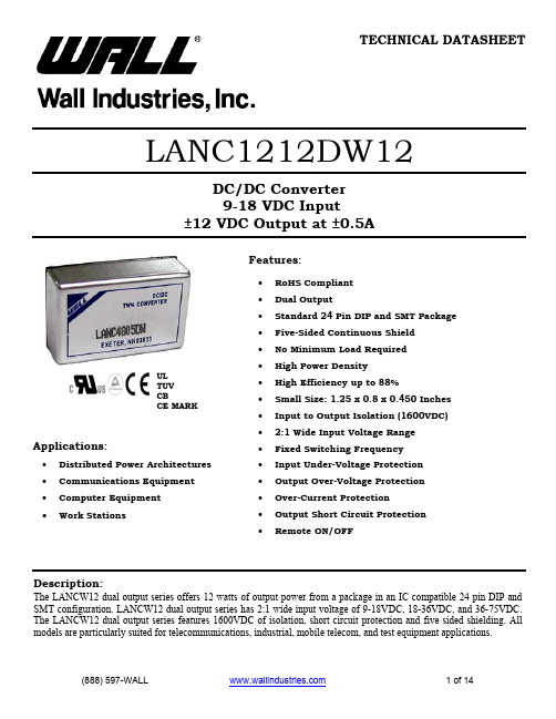
The LANCW12 dual output series offers 12 watts of output power from a package in an IC compatible 24 pin DIP and SMT configuration. LANCW12 dual output series has 2:1 wide input voltage of 9-18VDC, 18-36VDC, and 36-75VDC. The LANCW12 dual output series features 1600VDC of isolation, short circuit protection and five sided shielding. All models are particularly suited for telecommunications, industrial, mobile telecom, and test equipment applications.
Mellanox SX1012 ToR 交换机产品介绍说明书
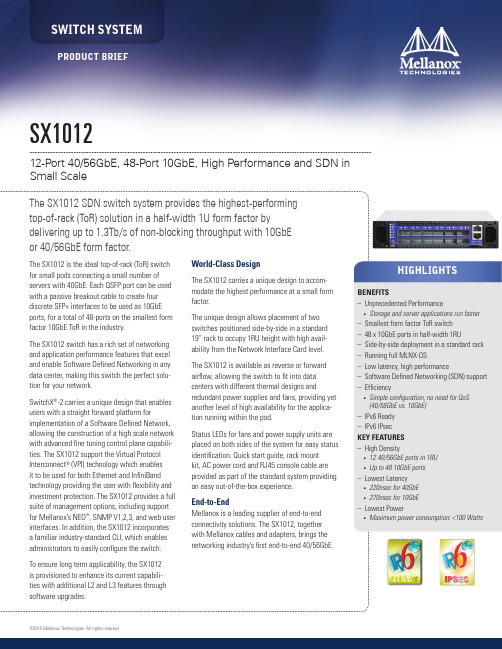
–– IPv6 Ready –– IPv6 IPsec KEY FEATURES –– High Density
• 12 40/56GbE ports in 1RU • Up to 48 10GbE ports –– Lowest Latency • 220nsec for 40GbE • 270nsec for 10GbE –– Lowest Power • Maximum power consumption: <100 Watts
©2015 Mellanox Technologies. All rights reserved.
SX1012 12-Port 40/56GbE, 48-Port 10GbE, High Performance and SDN in Small Scale
FEATURES
LAYER 2 FEATURE SET – 1GbE, 10GbE, 40GbE, 56GbE – 48K L2 Forwarding Entries – Static MAC – Jumbo Frames (9216 BYTES) – VLAN 802.1Q (4K) – 802.1W Rapid Spanning Tree Protocol
End-to-End Mellanox is a leading supplier of end-to-end connectivity solutions. The SX1012, together with Mellanox cables and adapters, brings the networking industry’s first end-to-end 40/56GbE.
LN5R12C_Datasheet_新浩科技

因VIN電阻長期承受輸入直流高壓, 應用中應確保電阻耐壓能力滿足要求, 一個較好的做法是使用兩個電阻串聯使 用,例如兩個 1206 型電阻串聯。
TO Ø VCC 過壓與欠壓保護 IC具有帶遲滯的欠電壓保護功 能。在啟動電流將VCC電壓充電達到 XOPY 8.9V時IC開始啟動,初始啟動電流由內 部高壓電流源提供,啟動后的VCC電壓 降開始由輔助繞組在電源反激期間提 供需要的能量。在IC 正常工作時應保 持VCC電壓在5-9V之間(包括滿負載輸 出的情況),若VCC電壓下降到3.5V則 振盪器將被關斷,直至VCC電壓下降至 2.0V電路開始重新啟動。 IC內部VCC具有一個上限電壓比較 器控制,若VCC 試圖大於10V,則比較 器動作,FB將被下拉,鎖定VCC至10V, 達到過電壓的限制功能。利用此功能可
特性作為反饋方式則可借此實現簡單的初
新級側穩壓控制方式。
5、降頻控制電路
隨著負載降低電路會逐漸降低系統的 工作頻率,從而改善輕載效率,同時降低 待機狀態下的功耗。
6、高效的驅動電路
高效的驅動電路使開關管始終工作於 臨界飽和驅動狀態,提高三極管的開關速 度,從而有效地減小了三極管的開關損 耗,提高整個系統的工作效率同時大大減 小了芯片的發熱,使系統工作更可靠。
電源部分:
符號
說明
IST IQ VST VSTOP VRST VSZ
啟動靜態電流 靜態電流 啟動電壓 欠壓保護點 重啟動電壓
VCC 限制電壓
測試條件
最小 典型 最大 單位
-
65
- kHz
Vcc=5-9V
-
-
1%
Ta=0-85℃
-
ADC122S051CIMMNOPB;ADC122S051CIMMXNOPB;中文规格书,Datasheet资料

ADC122S051/ADC122S051QJanuary 5, 2012 2 Channel, 200 ksps to 500 ksps 12-Bit A/D ConverterGeneral DescriptionThe ADC122S051/ADC122S051Q is a low-power, two-chan-nel CMOS 12-bit analog-to-digital converter with a high-speed serial interface. Unlike the conventional practice of specifying performance at a single sample rate only, the AD-C122S051/ADC122S051Q is fully specified over a sample rate range of 200 ksps to 500 ksps. The converter is based on a successive-approximation register architecture with an internal track-and-hold circuit. It can be configured to accept one or two input signals at inputs IN1 and IN2.The output serial data is straight binary, and is compatible with several standards, such as SPI™, QSPI™, MICROWIRE, and many common DSP serial interfaces.The ADC122S051/ADC122S051Q operates with a single supply that can range from +2.7V to +5.25V. Normal power consumption using a +3V or +5V supply is 3.0 mW and 10 mW, respectively. The power-down feature reduces the pow-er consumption to just 0.14 µW using a +3V supply, or 0.32µW using a +5V supply.The ADC122S051/ADC122S051Q is packaged in an 8-lead MSOP package. Operation over the industrial temperature range of −40°C to +85°C is guaranteed.Features■Specified over a range of sample rates.■Two input channels■Variable power management■Single power supply with 2.7V - 5.25V range■Tested per AEC-Q100 and qualified for automotive applications■Meets AEC-Q100-011 C2 CDM classificationKey Specifications■DNL+0.7 / −0.4 LSB (typ)■INL± 0.50 LSB (typ)■SNR72.5 dB (typ)■Power Consumption■—3V Supply 3.0 mW (typ)—5V Supply10 mW (typ) Applications■Portable Systems■Remote Data Acquisition■Instrumentation and Control SystemsPin-Compatible Alternatives by Resolution and SpeedAll devices are fully pin and function compatible.Resolution Specified for Sample Rate Range of:50 to 200 ksps200 to 500 ksps500 ksps to 1 Msps12-bit ADC122S021ADC122S051ADC122S10110-bit ADC102S021ADC102S051ADC102S1018-bit ADC082S021ADC082S051ADC082S101 Connection Diagram20106405Ordering InformationOrder Code Temperature Range Top Mark DescriptionADC122S051CIMM−40°C to +85°C X06C8-Lead MSOP PackageADC122S051CIMMX−40°C to +85°C X06C8-Lead MSOP Package, Tape & ReelADC122S051QIMM−40°C to +85°C X06Q8-Lead MSOP Package, AEC-Q100 (Note 11)ADC122S051QIMMX−40°C to +85°C X06Q8-Lead MSOP Package, Tape & Reel, AEC-Q100 (Note 11) ADC122S051EVAL Evaluation BoardTRI-STATE® is a trademark of National Semiconductor CorporationQSPI™ and SPI™ are trademarks of Motorola, Inc.© 2012 Texas Instruments Incorporated201064 SNAS257D ADC122S051/ADC122S051Q 2 Channel, 200 ksps to 500 ksps 12-Bit A/D ConverterBlock Diagram20106407Pin Descriptions and Equivalent CircuitsPin No.SymbolDescriptionANALOG I/O5,4IN1 and IN2Analog inputs. These signals can range from 0V to V A .DIGITAL I/O8SCLK Digital clock input. This clock directly controls the conversion and readout processes.7DOUT Digital data output. The output samples are clocked out of this pin on falling edges of the SCLK pin.6DIN Digital data input. The ADC122S051/ADC122S051Q's Control Register is loaded through this pin on rising edges of the SCLK pin.1CSChip select. On the falling edge of CS, a conversion process begins. Conversions continue as long as CS is held low.POWER SUPPLY2V A Positive supply pin. This pin should be connected to a quiet +2.7V to +5.25V source and bypassed to GND with a 1 µF capacitor and a 0.1 µF monolithic capacitor located within 1 cm of the power pin.3GNDThe ground return for the die. 2A D C 122S 051/A D C 122S 051QAbsolute Maximum Ratings (Note 1, Note 2)If Military/Aerospace specified devices are required, please contact the Texas Instruments Sales Office/ Distributors for availability and specifications.Analog Supply Voltage VA−0.3V to 6.5VVoltage on Any Pin to GND−0.3V to VA+0.3V Input Current at Any Pin (Note 3)±10 mA Package Input Current (Note 3)±20 mAPower Consumption at TA= 25°C See (Note 4)ESD Susceptibility (Note 5) Human Body ModelMachine ModelCharged Device Model 2500V 250V 500VJunction Temperature+150°C Storage Temperature−65°C to +150°C Operating Ratings (Note 1, Note 2) Operating Temperature Range−40°C ≤ T A≤ +85°C VASupply Voltage+2.7V to +5.25V Digital Input Pins Voltage Range−0.3V to V A Clock Frequency50 kHz to 16 MHz Analog Input Voltage0V to V A Package Thermal ResistancePackageθJA8-lead MSOP250°C / WS o ldering pr o cess must c o mply with Nati o nal Semiconductor's Reflow Temperature Profile specifications. Refer to /packaging. (Note 6)ADC122S051/ADC122S051Q Converter Electrical Characteristics (Note 9)The following specifications apply for VA = +2.7V to 5.25V, GND = 0V, fSCLK= 3.2 MHz to 8 MHz, fSAMPLE= 200 ksps to 500 ksps,C L = 35 pF unless otherwise noted. Boldface limits apply for TA= TMINto TMAX: all other limits TA= 25°C.Symbol Parameter Conditions TypicalLimits(Note 7)UnitsSTATIC CONVERTER CHARACTERISTICSResolution with No Missing Codes12Bits INL Integral Non-Linearity±0.5±1.1LSB (max)DNL Differential Non-Linearity +0.7 1.3LSB (max)−0.4−1.0LSB (min)VOFFOffset Error+0.3±1.3LSB (max) OEM Channel to Channel Offset Error Match±0.1±1.0LSB (max) FSE Full Scale Error−0.5±1.5LSB (max)FSEM Channel to Channel Full-Scale ErrorMatch+0.01±1.0LSB (max)DYNAMIC CONVERTER CHARACTERISTICSSINAD Signal-to-Noise Plus Distortion Ratio VA= +2.7 to 5.25VfIN= 40.2 kHz, −0.02 dBFS7269.2dB (min)SNR Signal-to-Noise Ratio VA= +2.7 to 5.25VfIN= 40.2 kHz, −0.02 dBFS72.570.6dB (min)THD Total Harmonic Distortion VA= +2.7 to 5.25VfIN= 40.2 kHz, −0.02 dBFS−84−75dB (max)SFDR Spurious-Free Dynamic Range VA= +2.7 to 5.25VfIN= 40.2 kHz, −0.02 dBFS8676dB (min)ENOB Effective Number of Bits V A = +2.7 to 5.25V11.711.2Bits (min)Channel-to-Channel Crosstalk VA= +5.25VfIN= 40.2 kHz−86dBIMD Intermodulation Distortion, SecondOrder TermsVA= +5.25V,fa= 40.161 kHz, fb= 41.015 kHz−87dB Intermodulation Distortion, Third OrderTermsVA= +5.25Vfa= 40.161 kHz, fb= 41.015 kHz−88dBFPBW-3 dB Full Power Bandwidth VA= +5V11MHzVA= +3V8MHzADC122S051/ADC122S051QSymbol Parameter Conditions TypicalLimits (Note 7)UnitsANALOG INPUT CHARACTERISTICS V IN Input Range 0 to V A V I DCL DC Leakage Current±0.02±1µA (max)C INAInput CapacitanceTrack Mode 33pF Hold Mode 3 pF DIGITAL INPUT CHARACTERISTICS V IH Input High Voltage V A = +5.25V 2.4 V (min)V A = +3.6V 2.1V (min)V IL Input Low Voltage0.8 V (max)I IN Input CurrentV IN = 0V or V IN = V A ±0.02±10µA (max)C INDDigital Input Capacitance24pF (max)DIGITAL OUTPUT CHARACTERISTICS V OH Output High Voltage I SOURCE = 200 µA V A − 0.03V A − 0.5V (min)I SOURCE = 1 mA V A − 0.10 V V OL Output Low VoltageI SINK = 200 µA 0.020.4V (max)I SINK = 1 mA 0.1 V I OZH , I OZL TRI-STATE® Leakage Current 0.005±1µA (max)C OUT TRI-STATE® Output Capacitance 24pF (max)Output CodingStraight (Natural) BinaryPOWER SUPPLY CHARACTERISTICS (C L = 10 pF)V AAnalog Supply Voltage2.7V (min)5.25V (max)I ASupply Current, Normal Mode (Operational, CS low)V A = +5.25V,f SAMPLE = 500 ksps, f IN = 40 kHz 1.9 2.4mA (max)V A = +3.6V,f SAMPLE = 500 ksps, f IN = 40 kHz 0.84 1.2mA (max)Supply Current, Shutdown (CS high)V A = +5.25V,f SAMPLE = 0 ksps 60nA V A = +3.6V,f SAMPLE = 0 ksps 38nAP DPower Consumption, Normal Mode (Operational, CS low)V A = +5.25V 1012.6mW (max)V A = +3.6V 3.0 4.3mW (max)Power Consumption, Shutdown (CS high)V A = +5.25V 0.32µW V A = +3.6V0.14µWAC ELECTRICAL CHARACTERISTICS f SCLK Maximum Clock Frequency (Note 8) 3.2MHz (min)8MHz (max)f S Sample Rate (Note 8) 200ksps (min)500ksps (max)t CONV Conversion Time13SCLK cycles DC SCLK Duty Cyclef SCLK = 8 MHz 5030% (min)70% (max)t ACQ Track/Hold Acquisition Time Full-Scale Step Input3SCLK cyclesThroughput TimeAcquisition Time + Conversion Time16SCLK cycles 4A D C 122S 051/A D C 122S 051QADC122S051/ADC122S051Q Timing SpecificationsThe following specifications apply for V A = +2.7V to 5.25V, GND = 0V, f SCLK = 3.2 MHz to 8 MHz, f SAMPLE = 200 ksps to 500 ksps,C L = 35 pF, Boldface limits apply for T A = T MIN to T MAX : all other limits T A = 25°C.Symbol ParameterConditionsTypical Limits (Note 7)Units t CSU Setup Time SCLK High to CS Falling Edge (Note 10)V A = +3.0V −3.510ns (min)V A = +5.0V −0.5t CLH Hold time SCLK Low to CS Falling Edge (Note 10)V A = +3.0V +4.510ns (min)V A = +5.0V +1.5t EN Delay from CS Until DOUT activeV A = +3.0V +430ns (max)V A = +5.0V +2t ACC Data Access Time after SCLK Falling Edge V A = +3.0V +14.530ns (max)V A = +5.0V+13t SU Data Setup Time Prior to SCLK Rising Edge +310ns (min)t H Data Valid SCLK Hold Time +310ns (min)t CH SCLK High Pulse Width 0.5 x t SCLK 0.3 x t SCLK ns (min)t CLSCLK Low Pulse Width0.5 x t SCLK 0.3 x t SCLK ns (min)t DISCS Rising Edge to DOUT High-ImpedanceOutput FallingV A = +3.0V 1.820ns (max)V A = +5.0V 1.3Output RisingV A = +3.0V 1.0V A = +5.0V 1.0Note 1:Absolute Maximum Ratings indicate limits beyond which damage to the device may occur. Operating Ratings indicate conditions for which the device is functional, but do not guarantee specific performance limits. For guaranteed specifications and test conditions, see the Electrical Characteristics. The guaranteed specifications apply only for the test conditions listed. Some performance characteristics may degrade when the device is not operated under the listed test conditions.Note 2:All voltages are measured with respect to GND = 0V, unless otherwise specified.Note 3:When the input voltage at any pin exceeds the power supply (that is, V IN < GND or V IN > V A ), the current at that pin should be limited to 10 mA. The 20mA maximum package input current rating limits the number of pins that can safely exceed the power supplies with an input current of 10 mA to two. The Absolute Maximum Rating specification does not apply to the V A pin. The current into the V A pin is limited by the Analog Supply Voltage specification.Note 4:The absolute maximum junction temperature (T J max) for this device is 150°C. The maximum allowable power dissipation is dictated by T J max, the junction-to-ambient thermal resistance (θJA ), and the ambient temperature (T A ), and can be calculated using the formula P D MAX = (T J max − T A )/θJA . The values for maximum power dissipation listed above will be reached only when the device is operated in a severe fault condition (e.g. when input or output pins are driven beyond the power supply voltages, or the power supply polarity is reversed). Obviously, such conditions should always be avoided.Note 5:Human body model is 100 pF capacitor discharged through a 1.5 k Ω resistor. Machine model is 220 pF discharged through zero ohms Note 6:Reflow temperature profiles are different for lead-free and non-lead-free packages.Note 7:Tested limits are guaranteed to National's AOQL (Average Outgoing Quality Level).Note 8:This is the frequency range over which the electrical performance is guaranteed. The device is functional over a wider range which is specified under Operating Ratings.Note 9:Min/max specification limits are guaranteed by design, test, or statistical analysis.Note 10:Clock may be either high or low when CS is asserted as long as setup and hold times t CSU and t CLH are strictly observed.Note 11:PPAP (Production Part Approval Process) documentation of the device technology, process and qualification is available from Texas Instruments upon request.ADC122S051/ADC122S051QTiming Diagrams20106451Operational Timing Diagram20106408Timing Test Circuit20106406Serial Timing Diagram20106450SCLK and CS Timing Parameters 6A D C 122S 051/A D C 122S 051QSpecification DefinitionsACQUISITION TIME is the time required to acquire the input voltage. That is, it is time required for the hold capacitor to charge up to the input voltage.APERTURE DEL AY is the time between the fourth falling SCLK edge of a conversion and the time when the input signal is acquired or held for conversion.CONVERSION TIME is the time required, after the input volt-age is acquired, for the ADC to convert the input voltage to a digital word.CROSSTALK is the coupling of energy from one channel into the other channel, or the amount of signal energy from one analog input that appears at the measured analog input.DIFFERENTIAL NON-LINEARITY (DNL) is the measure of the maximum deviation from the ideal step size of 1 LSB.DUTY CYCLE is the ratio of the time that a repetitive digital waveform is high to the total time of one period. The specifi-cation here refers to the SCLK.EFFECTIVE NUMBER OF BITS (ENOB, or EFFECTIVE BITS) is another method of specifying Signal-to-Noise and Distortion or SINAD. ENOB is defined as (SINAD − 1.76) /6.02 and says that the converter is equivalent to a perfect ADC of this (ENOB) number of bits.FULL POWER BANDWIDTH is a measure of the frequency at which the reconstructed output fundamental drops 3 dB below its low frequency value for a full scale input.FULL SCALE ERROR (FSE) is a measure of how far the last code transition is from the ideal 1½ LSB below V REF + and is defined as:V FSE = V max + 1.5 LSB – V REF +where V max is the voltage at which the transition to the maxi-mum code occurs. FSE can be expressed in Volts, LSB or percent of full scale range.GAIN ERROR is the deviation of the last code transition (111...110) to (111...111) from the ideal (V REF − 1.5 LSB), af-ter adjusting for offset error.INTEGRAL NON-LINEARITY (INL) is a measure of the de-viation of each individual code from a line drawn from negative full scale (½ LSB below the first code transition) through pos-itive full scale (½ LSB above the last code transition). The deviation of any given code from this straight line is measured from the center of that code value.INTERMODULATION DISTORTION (IMD) is the creation of additional spectral components as a result of two sinusoidalfrequencies being applied to the ADC input at the same time.It is defined as the ratio of the power in the second and third order intermodulation products to the sum of the power in both of the original frequencies. IMD is usually expressed in dB.MISSING CODES are those output codes that will never ap-pear at the ADC outputs. These codes cannot be reached with any input value. The ADC122S051/ADC122S051Q is guar-anteed not to have any missing codes.OFFSET ERROR is the deviation of the first code transition (000...000) to (000...001) from the ideal (i.e. GND + 0.5 LSB).SIGNAL TO NOISE RATIO (SNR) is the ratio, expressed in dB, of the rms value of the input signal at the converter output to the rms value of the sum of all other spectral components below one-half the sampling frequency, not including d.c. or harmonics included in the THD specification.SIGNAL TO NOISE PL US DISTORTION (S/N+D or SINAD) Is the ratio, expressed in dB, of the rms value of the input signal to the rms value of all of the other spectral com-ponents below half the clock frequency, including harmonics but excluding d.c.SPURIOUS FREE DYNAMIC RANGE (SFDR) is the differ-ence, expressed in dB, between the desired signal amplitude to the amplitude of the peak spurious spectral component,where a spurious spectral component is any signal present in the output spectrum that is not present at the input and may or may not be a harmonic.TOTAL HARMONIC DISTORTION (THD) is the ratio, ex-pressed in dB or dBc, of the rms total of the first five harmonic components at the output to the rms level of the input signal frequency as seen at the output. THD is calculated aswhere A f1 is the RMS power of the input frequency at the out-put and A f2 through A f6 are the RMS power in the first 5harmonic frequencies. Accurate THD measurement requires a spectrally pure sine wave (monotone) at the ADC input.THROUGHPUT TIME is the minimum time required between the start of two successive conversion. It is the acquisition time plus the conversion and read out times. In the case of the ADC122S051/ADC122S051Q, this is 16 SCLK periods.ADC122S051/ADC122S051QTypical Performance CharacteristicsT A = +25°C, f SAMPLE = 200 ksps to 500 ksps, f SCLK = 3.2 MHz to8 MHz, f IN = 40.2 kHz unless otherwise stated.DNL - V A = 3.0V20106420INL - V A = 3.0V20106421DNL - V A = 5.0V 20106462INL - V A = 5.0V20106463DNL vs. Supply 20106422INL vs. Supply20106423 8A D C 122S 051/A D C 122S 051QDNL vs. Clock Frequency20106424INL vs. Clock Frequency20106425DNL vs. Clock Duty Cycle20106426INL vs. Clock Duty Cycle20106427DNL vs. Temperature20106428INL vs. Temperature20106429ADC122S051/ADC122S051QSNR vs. Supply 20106430THD vs. Supply20106435SNR vs. Clock Frequency 20106431THD vs. Clock Frequency20106436SNR vs. Clock Duty Cycle 20106432THD vs. Clock Duty Cycle20106437 10A D C 122S 051/A D C 122S 051Q分销商库存信息: NATIONAL-SEMICONDUCTORADC122S051CIMM/NOP B ADC122S051CIMMX/NO PB。
频谱仪

手持频谱仪用户手册与操作指南
Spectrum Master
Байду номын сангаас
MS2721 B MS2723 B MS2724 B
9 kHz ~ 7.1 GHz 9 kHz ~ 13 GHz 9 kHz ~ 20 GHz
MS2721B, MS2723B, MS2724B Spectrum Master 手持式频谱仪 用户手册与操作指南
衰 减 器 功 能 ...................................................................................................4-2 前 置 放 大 器 的 操 作 ......................................................................................4-2 第5章 现场测试(单键智能测试) .....................................................................5-1 本章内容介绍 .................................................................................................5-1 占用带宽测量(OBW) ................................................................................5-1 信道功率测量(Channel Power).................................................................5-2 CDMA信 道 功 率 ...........................................................................................5-3 CDMA信 道 功 率 测 量 ..................................................................................5-3 GSM信 道 功 率 测 量 ......................................................................................5-4 临 道 功 率 比 (ACPR) ...............................................................................5-5 临 道 功 率 比 测 量 ...........................................................................................5-5 GSM临 道 功 率 比 测 量 .................................................................................5-6 带 外 杂 散 辐 射 测 量 ......................................................................................5-7 带 内/信 道 外 测 量 .........................................................................................5-8 带 内 杂 散 的 测 量 ...........................................................................................5-8 场 强 测 量 ......................................................................................................5-10 AM/FM/SSB解 调 .......................................................................................5-11 C/I( 载 干 比 ) 测 量 ...................................................................................5-11 第6章 干扰分析测量 .............................................................................................6-1 本章内容介绍 .................................................................................................6-1 Measurements(测量)菜单 ..........................................................................6-2 Spectrum(频谱)菜单 ..................................................................................6-3 Spectrogram( 三 维 频 谱 图 ) 菜 单 ...........................................................6-4 Signal Strength( 信 号 强 度 ) 菜 单 ..........................................................6-5 RSSI( 接 收 信 号 强 度 指 示 ) 菜 单 ...........................................................6-7 Marker(光标)菜单 ..................................................................................6-8 Spectrogram( 三 维 频 谱 图 ) 测 量 步 骤 ................................................6-10 Signal Strength( 信 号 强 度 ) 测 量 步 骤 ................................................6-12 RSSI( 接 收 信 号 强 度 指 示 ) 测 量 步 骤 .................................................6-13 第7章 信道扫描测量 .............................................................................................7-1 本章内容介绍 .................................................................................................7-1 Scanner(扫描)菜单.....................................................................................7-2 幅度(Amplitude)菜单 ................................................................................7-4 用户设置(Custom Setup)菜单...................................................................7-4 测量(Measurements)菜单 ..........................................................................7-5 测量步骤示例 .................................................................................................7-7 用户设置步骤 .................................................................................................7-8 第8章 跟踪信号源 .................................................................................................8-1 本章内容介绍 .................................................................................................8-1 菜单结构 .........................................................................................................8-1
C1225中文资料

Max
Unit V GHz V V V V Ω Ω Ω
Comments @100µA
Physical Characteristics
66
C1225-4-98
元器件交易网
Process C1225
Physical Characteristics
Starting Material Starting Mat. Resistivity Typ. Operating Voltage Well Type Metal Layers Poly Layers Contact Size Via Size Metal-1 Width/Space Metal-2 Width/space Gate Poly Width/Space
p <100> 25 - 50 Ω-cm 5V Twin well 2 1 1.5x1.5µm 1.5x1.5µm 2.5 / 1.5µm 2.5 / 1.5µm 1.5 / 2.0µm
N+/P+ Width/Space N+ to P+ Space Contact to Poly Space Contact Overlap of Diffusion Contact Overlap of Poly Metal-1 Overlap of Contact Metal-1 Overlap of Via Metal-2 Overlap of Via Minimum Pad Opening Minimum Pad-to-Pad Spacing Minimum Pad Pitch
Maximum 1.57
Unit fF/µm2 fF/µm2 fF/µm2 fF/µm2
Comments
© IMP, Inc.
大华高清圈灯海螺型网络摄像机_使用说明书_V1.3.3
特别声明
产品请以实物为准,说明书仅供参考。 说明书将根据产品的变化定期更新,更新的内容将会在本手册的新版本中加入,恕不另行通知。产品
RESOL VBus LAN接口适配器用户手册说明书
VBus ®/LAN interface adapterMounting Connection Operation*48005480*48005480Thank you for buying this RESOL product.Read this manual carefully to get the best perfomance from this unit.Please keep this manual carefully.VBus ®/LAN interface adapter© R E S O L _10046_V B u s /L A N _m o n e n .i n d d|2Proper usageThe RESOL V Bus ®/LAN interface adapter may only be used for connecting an electronic controller for solar thermal sy-stems to a computer network or PC via the RESOL VBus ® in compliance with the technical data specified in these instructions.Improper use excludes all liability claims.GeneralInhaltGeneral .....................................................................2Overview ...................................................................3Technical data ..............................................................................31. Mounting ..............................................................42. Connection ..........................................................53. System access via RSC-Software .....................63.1 Data logging ...........................................................................63.2 Parametrization .. (7)4. Network settings ................................................75. Reset.....................................................................96. LED displays ........................................................96.1 LED at the front of the housing .......................................96.2 Status LEDs at the RJ45 LAN connector ..............................9Glossary ..................................................................10Imprint .. (12)Subject to technical change. Errors excepted.Description of symbolsDisposalSignal words describe the danger that may occur, when it is not avoided.Warning means that injury, possibly life-threatening injury, can occur.Attention means that damage to the appliance can occur.Dispose of the packaging in an environmentally sound •manner.Dispose of old appliances in an environmentally sound •manner. Upon request we will take back your olda ppliances bought from us and guarantee an environ-mentally sound disposal of the rmation about the productCE-Declaration of conformityThe product complies with the relevant di-rectives and is therefore labelled with the CE mark. The Declaration of Conformity is availa-ble upon request, please contact RESOL.NoteNotes are indicated with an information symbol.Arrows indicate instruction steps that should be Îcarried out.Safety advicePlease pay attention to the following safety advice in order to avoid danger and damage to people and property.InstructionsAttention must be paid to the valid local standards, regu-lations and directives!This manual contains important information about safe and proper usage of this product. Please keep this manual for future reference.NoteStrong electromagnetic fields can impair the function of the device.Make sure the device is not exposed to Îstrong electromagnetic fields.VBus ®/LAN interface adapter© R E S O L _10046_V B u s /L A N _m o n e n .i n d d3|The network connection for your solar system •Access to the system via the complete network •Remote parametrisation of the controller via •VBus ®Full version of the RSC software included on •CD-ROMOverviewVBus ®/LAN interface adapterThe VBus ®/LAN interface adapter is designed for the con-necting the controller directly to a PC or router. It enables easy access to the controller via the local network of the owner. Thus, controller access, system parametrisation and data charting can be effected from every workstation of the network.The VBus ®/LAN interface adapter is designed for the con-nection to controllers equipped with a RESOL VBus ®.T echnical dataHousing: plasticProtection type: IP 20 (EN 60529)Ambient temperature: 0 ... 40 °C Dimensions: 95 × 70 × 25 mmMounting: Wall mounting is possible (but not required)Display:1 bi-coloured LED at the front of the housing2 LEDs at the RJ45 connection Power supply: Mains power supply:220 ... 240 V~ / 50-60 Hz Mains adapter: power supply:12 V / 0,5 A 5.5 x 2.5 mm Interface: RESOL VBus ®RJ45 LAN connectionSupported Operating Systems:Windows XP , Windows Vista, Windows 7Included:1 × Mains adapter 12 V / 0.5 A / 5.5 x 2.5 mm 1 × VBus ® cable, 1.5 m1 × Cat 5 LAN cable, screened,2 m 1 × RSC-CD1 × Accessory bag containing2 × Screw and wall plug 4 × Self-adhesive, skid-proof rubber padVBus ®/LAN interface adapter© R E S O L _10046_V B u s /L A N _m o n e n .i n d d| 41. MountingThe unit must only be located in dry interior locations. It is not suitable for installation in hazardous locations. Please pay attention to separate routing of sensor cables and mains cables.The interface adapter is light and small and thus does not require any form of mounting. It can be placed on a suitable surface (pay attention to the ambient temperature!).Four self-adhesive, skid-proof rubber pads are included with the V Bus ®/LAN interface adapter. If necessary, these can be affixed to the corresponding molds on the base part of the housing to ensure a secure placement of the device without wall mounting.If desired, the interface adapter can be mounted to a wall:Mark the desired hanging position on the wall ÎDrill and prepare the hole with a wall plug and screw ÎHang the device onto the screwÎMark the position for the mounting screw (distance to Îhanging point centre: 70 mm)Drill and prepare a hole with a wall plugÎAttach the device and fasten it by means of the second ÎscrewFor wall mounting, opening the housing is not required. Opening the housing is only required for access to the terminals.To open the housing, unscrew the cover screw and pull Îoff the upper part of the housing To close the housing again, relocate the upper part of Îthe housing and refasten the cover screwESD damage!Electrostatic discharge can lead to da-mage to electronic components!Take care to discharge properly before touching the inside of the device. To do so, touch a grounded surface such as a radiator or tap!Front viewBack viewOpening for the mounting screwHangingMolds for the rubber padsCover screwUpper part of the housingBase part of the housingVBus ®/LAN interface adapter© R E S O L _10046_V B u s /L A N _m o n e n .i n d d5|RJ45 LAN connectorMains connectorVBus ® terminals bi-colouredfront-LEDStatus-LEDsReset buttonThe VBus ®/LAN interface adapter needs a mains, a VBus ® and a LAN connection to function. To install the VBus ® cable, the housing has to be opened (see chap. 1).Connect the included VBus ή cable to the VBus ® termi-nals with either polarityThe VBus ® cable can be extended or replaced with a two-wire cable (bell wire). The cross section of the cable must be at least 0.5 mm 2 and the cable can be extended up to 50 m in the case that one module is used.Depending on whether you want to access your solar system or adjust the network settings, the VBus ®/LAN interface adapter can be accessed in two different ways:In order to •access the solar system via the RESOLS erviceCenter Software (data processing and re-mote parametrisation of the controller, see chap. 3), the VBus ®/LAN interface adapter has to be accessed via the RESOL ServiceCenter Software.In order to adjust the •network settings (retrieving and changing the IP address, changing the device name and password, see chap. 4), the VBus ®/LAN interface adapter has to be accessed via the operating system of the computer. To make these adjustments possible, the UPnP access has to be enabled.Interior view of the VBus ®/LAN interior adapter2. ConnectionShort circuit!A short circuit can lead to damage to electronic components!Finish terminal connection and clo-se the housing before establishingthe mains connection!Close the housing (see chap. 1)ÎEstablish the network connection by means of the Îincluded LAN cableEstablish the mains connection by means of the inclu- Îded mains adapterVBus ®/LAN interface adapter© R E S O L _10046_V B u s /L A N _m o n e n .i n d d| 63. System access via RSC-SoftwareWith the RESOL ServiceCenter Software, the controller can be configured and system data can be recorded via the VBus ®/LAN interface adapter. A CD-ROM containing the RSC software is included with the device.Install the software on at least one computer in the ÎnetworkFor more information about the installation see the RSC software manual.3.1 Data loggingIn order to log data via the RSC software, proceed as follows:Start the RESOL ServiceCenter software ÎClick on the ÎVBus Logging tab (Fig. 1)At the bottom of the page, in the drop-down menu ÎPort name , select Connect to VBus/LAN (Fig. 2)The window RESOL Device Discoveryappears (Fig. 3).Fig. 1Fig. 2Fig. 3In the upper-hand menu, select the VBus ή/LAN inter-face adapterType the password into the ÎVBus/LAN Remote Password input field (see chap. 4)Click on ÎOKThe window RESOL Device Discovery closes. In the VBus Logging tab of the RSC software, the incoming data of the controller appear and can be processed.For more information about data processing see the RSC software manual.VBus ®/LAN interface adapter© R E S O L _10046_V B u s /L A N _m o n e n .i n d d7|4. Network settingsIn order to access the web interface of the VBus ®/LAN interface adapter, proceed as follows:Select ÎComputer (Windows XP: Start / Settings) in the Start menuClick on ÎNetwork (XP: Network connections)The VBus ®/LAN interface adapter appears under Other Devices (Fig.6; XP: My Network Places).NoteAlways ask a skilled system administrator to change the IP address and UPnP port number!Fig. 63.2 ParametrizationIn order to parametrise the controller via the RSC soft-ware proceed as follows:Open the RESOL ServiceCenter software ÎClick on the tab ÎParametrization (Fig. 4)Down to the right of the page, in the drop-down menu ÎPort name , select Connect to VBus/LAN In the next step, different actions are available:Read values:•The current controller data are transferred to the computer and can be processed there.Write values:•The data enetered in the software are transferred to the controller.Export values:• A HTML file with the current controller data is gene-rated and can be opened in a web browser, printed, or saved.Click on the action you want to perform (Fig. 5)ÎThe required input fields appear in the Parametrization tab of the RSC software.For more information about parametrization see the RSCsoftware manual.Fig. 4Fig. 5Double-click on the symbolÎThe Web-Interface appears in the browser window (Fig. 7).In order to access the VBus ®/LAN interface adapter via the operating system, the UPnP access has to be enabled.Under Windows Vista and Windows 7, the UPnP access is enabled by default. Under Windows XP, UPnP access can be enabled in Control Panel / Network connections / Advanced / Optional network components... / Network services / Details.NoteSome RESOL controllers cannot be parame-trized via the RSC software. In order to para-metrize these controllers, the additional tool integrated in the RSC software has to be used.VBus ®/LAN interface adapter© R E S O L _10046_V B u s /L A N _m o n e n .i n d d| 8Changing the module nameIn the same menu, a new module name can be assigned to the V Bus ® / L AN interface adapter. The device will be displayed with its module name in the network.Enter the desired name into the ÎModule Name input fieldClick on ÎUpdate Settings The new module name is saved.Fig. 8bThe Web-Interface is not designed for controller access, but for adjusting the network settings of the VBus ®/LAN interface adapter.By means of the Settings menu of the Web-Interface, the following settings can be adjusted:Assign a static IP address to the VBus •®/LAN interface adapterChange the name and the password of the V Bus •® / L AN interface adapterReset the VBus •®/LAN interface adapterSelect a menu language for the Web-Interface •Change the UPnP-port number•Changing the password The default password for the V Bus ® / L AN interface adapter is …vbus“. It can be changed in order to prevent unautho-rised access.To change the password, proceed as follows:Click on ÎSettings in the Web-InterfaceEnter the desired password into the ÎVBus Password input fieldClick on ÎUpdate Settings The new password is saved.Accessing the device is not possible without the correct password.Note down the new password and keep it carefully! ÎIf the password is lost, the device has to be reset to thefactory settings. For more information see chap. 5.Fig. 7Fig. 8aVBus ®/LAN interface adapter© R E S O L _10046_V B u s /L A N _m o n e n .i n d d9|6. LED displaysThe V Bus ®/LAN interface adapter has one bi-coloured LED at the front of the housing and two LEDs at the RJ45 LAN connector.6.1 LED at the front of the housingThe bi-coloured LED at the front of the housing indicates the current operating status of the VBus ®/LAN interface adapter:LED flashes green:Adapter is bootingLED is permanently green:Normal operation, access is now possibleStatic IP address / IP address obtained from a DHCP server LED slowly flashes green:Normal operation, access is now possible IP address has been assigned automatically LED irregularly flashes green:Normal operation, data trafficLED flashes red/green:Network connection okay, no VBus ® signal LED quickly flashes red:Reset in progressLED is permanently red:Reset completed6.2 Status LEDs at the RJ45 LAN connectorAt the RJ45 LAN connector there are two status LEDs which indicate the status of the network connection:10/100 Link / Activity LED:LED glows: Network connection ok, no data traffic LED flashes irregularly: data traffic Full duplex LED:LED glows: Full duplex active10/100 Link / Activity LED Full duplex LED5. ResetIf the password for the V Bus ® / L AN interface adapter is lost, the device has to be manually reset to the factory settings. In order to conduct a reset, proceed as follows:Open the housing (see chap. 1)ÎPress the reset button for 5 secondsÎDuring the reset process, the front-LED flashes red.As soon as the reset is completed, the LED switches to a permanent red.As soon as the LED switches to a permanent red, stop Îpressing the reset button!When the reset has been completed, close the housing Î(see chap. 1)The reset will set the device back to factory settings. All adjustments made in the Web-Interface (see chap. 4) will be lost and will have to be made again.VBus ®/LAN interface adapter© R E S O L _10046_V B u s /L A N _m o n e n .i n d d| 10GlossaryIn telecommunication engineering, different communication standards are defined by their directionality. Communication that can only occur in a definite direction from sender to receiver is called simplex , an example is radio broadcasting. If both parties can be sender or receiver, but never both at the same time, as for example in amateur radio, the com-munication is called half duplex . If all parties can send and receive data at the same time, such as it is in telephony, the communication is called full duplex . Like most network devices, the VBus ®/LAN interface adapter is capable of full duplex communication.Full duplexUniversal Plug and Play, short: UPnP , denotes a standard for cross-brand access to devices in an IP-based network. UPnPIP stands for Internet Protocol, the network standard on which the Internet and most local area networks are based. Each device inside the network is assigned with an IP address by means of which it can unmistakably be identified.An IP address according to the current IPv4 standard con-sists of 32 Bits, equalling a 32-digit binary number. To make them more clear, IPv4 addresses are commonly represented as four decimal numbers between 0 and 255, seperated by period marks, e. g. 130.094.122.195.IP addressA Local Area Network, short: LAN , is a delimited network of computers and other devices (e. g. printer, router or our own VBus ®/LAN interface adapter). A Local Area Network is not limited to a certain size or diversity.LANIn telecommunication engineering, a bus is a system for data transfer between different parties. The VBus ® is a field bus, developed by RESOL, which sends and receives data packets via a voltage signal and also supplies connected devices with extra-low voltage.VBus ®An interface is a connection, either between two pieces of equipment or between a person and a computer, Web stan-ding for the Internet. RESOL devices such as the VBus ®/LAN interface adapter or the DL2 Datalogger have an integrated software that can be opened and operated in every web browser. This software is called Web-Interface because it is an interface to the device that can be accessed via the Internet.Web-InterfaceRJ-connectors are standardised telecommunication cable connectors. The RJ-standard has been established by the US-american Federal Communications Commission (FCC), the letters RJ stand for Registered Jack.The commonly used LAN connectors are called RJ45-connectors. Other commonly used names are …ISDN plug“ for unscreened and …ethernet plug“ for screened connectors of this kind.RJ45Dynamic Host Configuration Protocol, short: DHCP , describes an Internet protocol that controls the automatic retrieval of IP addresses and other data in a network.DHCPVBus ®/LAN interface adapter ©RESOL_146_VBus/L AN_m onen.indd 11|NotesDistributed by:Please note:The design and the specifications are to be changed without notice.The illustrations may differ from the original product.RESOL - Elektronische Regelungen GmbHHeiskampstraße 1045527 Hattingen / GermanyT el.: +49 (0) 23 24 / 96 48 - 0Fax: +49 (0) 23 24 / 96 48 - 755 **************Reprinting / copyingThis mounting- and operation manual including all parts is copyrighted. Another use outside the copyright requires the approval of RESOL - Elektronische Regelungen GmbH. This especially applies for copies, translations, microfilms and the storage into electronic systems.Editor: RESOL - Elektronische Regelungen GmbH Important notice :We took a lot of care with the texts and drawings of this manual and to the best of our knowledge and consent. As faults can never be excluded, please note: Y our own calcu-lations and plans, under consideration of the current stan-dards and guidelines should only be basis for your projects.We don´t offer a guarantee for the completeness of the drawings and texts of this manual - they only represent some examples. They can only be used at your own risk. No liability is assumed for incorrect, incomplete or false information and / or the resulting damages.。
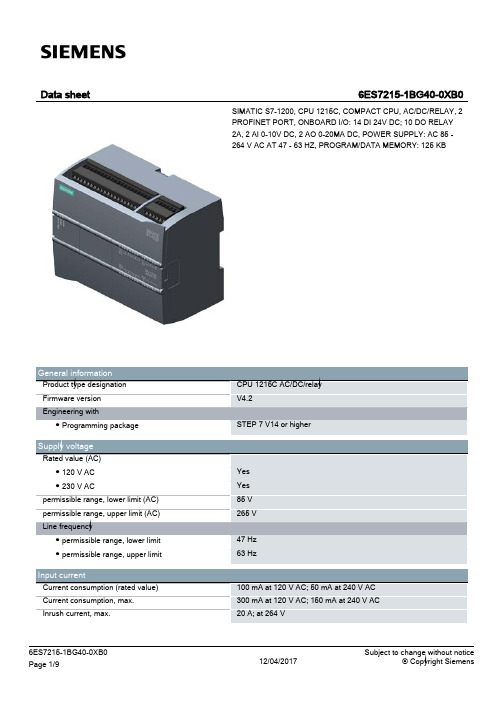
西门子SIMATIC S7-1200 CPU 1215C 产品数据表说明书
Yes Yes 85 V 265 V
47 Hz 63 Hz
100 mA at 120 V AC; 50 mA at 240 V AC 300 mA at 120 V AC; 150 mA at 240 V AC 20 A; at 264 V
12/04/2017
Subject to change without notice © Copyright Siemens
General information Product type designation Firmware version Engineering with ● Programming package
Supply voltage Rated value (AC) ● 120 V AC ● 230 V AC permissible range, lower limit (AC) permissible range, upper limit (AC) Line frequency ● permissible range, lower limit ● permissible range, upper limit
Yes
Single phase: 3 @ 100 kHz & 3 @ 30 kHz, differential: 3 @ 80 kHz & 3 @ 30 kHz
500 m; 50 m for technological functions 300 m; For technological functions: No
0.8 A²·s
1 600 mA; Max. 5 V DC for SM and CM
20.4 to 28.8V
14 W
125 kbyte No 4 Mbyte with SIMATIC memory card Yes Yes Yes
NcStudio V12 上下料控制系统 用户手册说明书

NcStudio V12上下料控制系统用户手册(第1版)上海维宏电子科技股份有限公司Weihong Electronic Technology Co., Ltd.The copyright of this manual belongs to Weihong Electronic Technology Co., Ltd. (hereinafter referred to as Weihong Company). This manual and any image, table, data or other information contained in this manual may not be reproduced, transferred, or translated without any prior written permission of Weihong Company.The information contained in this manual is constantly being updated. You can login to the official website of Weihong Company to download the latest PDF edition for free.本手册版权属于上海维宏电子科技股份有限公司所有。
未经本公司书面许可,任何人不得对此说明书和其中所包含的任何资料进行复制、拷贝或翻译成其它语言。
因印刷品具有一定滞后性,产品部分更新内容可能无法及时录入,由此给您带来的不便,敬请谅解。
如需了解最新版本的更新内容,可至维宏公司官网进行免费下载。
内容快速上手 (1)常用操作 (3)绝对值设置 (3)上下料操作 (4)换料操作 (4)手动换料 (6)上下料流程 (7)上下料相关参数 (8)润滑 (9)管理程序文件 (10)参数操作 (13)注册 (14)总线功能 (15)设置驱动器站地址 (15)安川驱动器 (15)维智驱动器 (17)设置驱动器参数 (18)调机过程 (20)安川驱动器 (20)调机前 (20)调机步骤说明 (20)调机失败 (21)维智驱动器 (21)调机前 (21)调机步骤说明 (22)调机失败 (22)V12设置驱动器参数 (23)V12自动调机 (24)功能介绍 (25)分中 (25)两点分中 (25)圆三点分中 (25)仿真功能 (26)手轮引导 (26)主轴预热与磨损 (26)日志功能 (26)用户指令(MDI) (26)丝杠误差补偿原理 (27)螺距误差 (27)丝杠误差补偿文件说明 (28)反向间隙误差 (29)系统维护 (30)制作安装包 (30)系统备份与还原 (30)使用U盘备份与还原 (31)常见问答 (36)软件安装过程中是否需要迁移参数? (36)上电开机后,端子板信号灯未亮,什么原因? (36)软件安装完成后,是否需要固件升级? (36)附录 (37)操作模式 (37)操作状态 (37)机械坐标系 (38)工件坐标系 (38)快速上手产品配置NcStudio V12上下料控制系统支持总线、非总线两种配置,对应使用的朗达控制器有所不同。
碧绿米仔兰叶的化学成分
碧绿米仔兰叶的化学成分张玲;张建辉;杨淑敏;谭昌恒【摘要】采用硅胶、Sephadex LH-20柱层析等方法,对碧绿米仔兰(Aglaia perviridis)的化学成分进行研究.从碧绿米仔兰叶的95%乙醇提取物中分离得到11个化合物,并通过1H-NMR,13C-NMR,MS等波谱技术鉴定了化合物的结构.【期刊名称】《上海大学学报(自然科学版)》【年(卷),期】2010(016)005【总页数】4页(P378-381)【关键词】楝科;碧绿米仔兰;化学成分【作者】张玲;张建辉;杨淑敏;谭昌恒【作者单位】上海大学,环境与化学工程学院,上海,200444;上海大学,环境与化学工程学院,上海,200444;中国科学院,上海药物研究所,上海,201203;首都医科大学,化学生物学与药学院,北京,100069【正文语种】中文【中图分类】O629Abstract:Column chromatographiesof silica gel and Sephadex LH-20 were used to isolate the chemical constituents of Aglaia perviridis.Eleven compoundswere isolated from the leavesof Aglaia perviridis,and their structures are identified on the basisof1H-NMR,13C-NMR and MS techniques.Key words:meliaceae;Aglaia perviridis;chemical constituents碧绿米仔兰 (Aglaia perviridis)系楝科(Meliaceae)米仔兰属 (Aglaia)植物,常绿乔木.米仔兰属植物主要分布于中国南部、印度和马来群岛以及太平洋岛地区,是印度和马来群岛热带雨林中的主要物种[1].米仔兰属的许多物种是传统的民间药物,如米仔兰 (Aglaia odorata),其叶味辛,微温,有活血散瘀、消肿止痛的功效,用于跌打、骨折、痈疮;其花味甘,性辛,有行气解郁的功能,用于气郁胸闷、食滞腹胀[2].东南亚部分地区 (如印度尼西亚)有将米仔兰属植物(如米仔兰)的花用做驱虫剂的传统.国外对米仔兰属植物化学成分的研究较为广泛.结果表明,从该属植物中所分离得到的有机化合物主要涉及环戊四氢苯并呋喃、双酰胺、木质素、三萜、甾体、四降三萜等,其中环戊四氢苯并呋喃类化合物具有显著的杀虫作用和抗肿瘤作用[3-7].虽然米仔兰为传统植物药,且米仔兰属植物中特有的 rocaglamide衍生物表现出显著的驱虫活性、抗肿瘤和抗炎活性,但在中药制备中却应用不足,国内也缺乏相关的基础研究.因而,对国内米仔兰属植物的化学成分及其生理活性成分进行研究是一项非常有意义的工作,可藉此发现具有药理活性的前体化合物用于药物研制,开发具有自主知识产权的新药或仿制药.本研究对碧绿米仔兰(采集于云南西双版纳)的化学成分进行分离,从其干燥叶子95%乙醇提取物的氯仿部位和醋酸乙酯部位共分离获得 11个化学成分.运用波谱技术鉴定了该化学成分的结构,分别为5,7,4′-三甲氧基双氢黄酮(Ⅰ)、5,7,4′-三甲氧基黄芪苷(Ⅱ)、5,7-二甲氧基 -4′-羟基双氢黄酮(Ⅲ)、胡椒碱(Ⅳ)、尿嘧啶(Ⅴ)、尿嘧啶核苷(Ⅵ)、对甲氧基苯甲酸(Ⅶ)、邻羟基对甲氧基苯甲酸(Ⅷ)、3,5-二甲氧基 -4-羟基苯甲酸(Ⅸ)、对羟基苯甲酸(Ⅹ)、β-胡萝卜苷(Ⅺ).化合物Ⅰ~Ⅺ的化学结构如图1所示.1.1 仪器与试剂Bruck AM-400核磁共振仪;MAT-95型质谱仪,LCQ-Deca型质谱仪,Q-Tof型质谱仪;200~300目硅胶;Sephadex LH-20葡聚糖凝胶.实验用碧绿米仔兰干叶采集于云南西双版纳,由中科院西双版纳热带植物园崔景云老师鉴定.1.2 提取与分离自然风干的碧绿米仔兰叶 5 kg粉碎,用 95%乙醇溶液 20 L室温浸泡,提取 3次,时间分别为 4,4和3 h.合并提取液,减压浓缩后得粗浸膏.所得浸膏用水分散后,依次用石油醚、氯仿、乙酸乙酯、正丁醇各萃取4次,浓缩,分别得石油醚部位、氯仿部位、乙酸乙酯部位和正丁醇部位.氯仿部位和乙酸乙酯部位经反复硅胶和 SephadexLH-20柱层析得化合物Ⅰ~Ⅺ.分离所得化合物Ⅰ~Ⅺ的波谱数据结果如下.化合物Ⅰ为无色晶体,MP为 124~126℃,分子式为 C18H20O5.1H-NMR(CDCl3,400 MHz)δ:7.39(2H,d,J=9.0 Hz,H-2′&6′),6.95(2H,d,J=9.0 Hz,H-3′&5′),6.14(1H,d,J=2.4 Hz,H-8),6.09(1H,d,J=2.4 Hz,H-6),5.36(1H,dd,J=12.9,2.1 Hz,H-2β),3.90,3.83,3.82(each 3H,s,3OCH3),3.05(1H,dd,J=16.4,13.2 Hz,H-3α),2.77(1H,dd,J=16.4,3.0 Hz,H-3β).ESI-MS(positive)m/z:337[M+Na]+,651[2M+Na]+.以上数据与文献[8]数据基本一致,鉴定为5,7,4′-三甲氧基双氢黄酮.化合物Ⅱ为淡黄色晶体,MP为 212~214℃,分子式为 C24H26O11.1H-NMR (Me2CO-d6,400 MHz)δ:6.53(1H,d,J=2.3 Hz,H-8),6.80(1H,d,J=2.3 Hz,H-6),7.08(2H,dd,J=7.8,2.4 Hz,H-3′&5′),8.26(2H,dd,J=7.8,2.4 Hz,H-2′&6′),3.97,3.93,3.90(each 3H,s,3 OMe),5.0(1H,d,J=7.4 Hz,H-1″),3.2~3.7(6H,m,H-2″,3″,4″,5″,6″).ESI-MS(postive)m/z:491[M+H]+,513[M+Na]+,1003[2M+Na]+.以上数据与文献[9]数据基本一致,鉴定为5,7,4′-三甲氧基黄芪苷.MHz)δ:7.33(2H,d,J=8.4 Hz,H-2′&6′),7.12(2H,d,J=8.4 Hz,H-3′&5′),6.14(1H,d,J=2.2 Hz,H-6),6.09(1H,d,J=2.2 Hz,H-8),5.36(1H,dd,J=13.0,2.8,H-2),3.05(1H,dd,J=16.5,13.0,H-3α),2.77(1H,dd,J=16.5,2.8,H-3β),3.92,3.98(each 3H,s,2 OMe).ESI-MS:323[M+Na]+,623[2M+Na]+,299[M-H]-.以上数据与文献[10]数据基本一致,鉴定为 5,7-二甲氧基 -4′-羟基双氢黄酮.化合物Ⅳ为无色晶体,分子式为 C17H19NO3,MP为 127~129℃.1H-NMR(CDCl3,400MHz)δ:7.40(1H,ddd,J=14.6,8.0,2.4 Hz,β-H),6.89(1H,dd,J=8.0,1.6 Hz,H-13),6.98(1H,d,J=1.6 Hz,H-17),6.78(1H,d,J=15.0 Hz,δ-H),6.78(1H,d,J=8.0 Hz,H-14),6.76(1H,dd,J=8.0,15.0 Hz,γ-H),6.44(1H,d,J=14.6 Hz,α-H),5.98(2H,s,CH2-18),3.64(2H,br.s,CH2-6),3.53(2H,br.s,CH2-2),1.70~1.55(6H,m,CH2-3,4,5).13C-NMR(C DCl3,100 MHz)δ:165.4(C-7),148.1(C-15&C-16),142.4(C-9),138.2(C-11),131.0(C-12),125.3(C-10),122.5(C-13),120.0(C-8),108.4(C-14),105.6(C-17),101.2(C-18),46.8(C-6),43.2(C-2),26.7(C-5),25.6(C-3),24.6(C-4).ESI-MS:m/z286[M+H]+;308[M+Na]+;593[2M+Na]+.以上数据与文献[11]数据基本一致,鉴定为胡椒碱.化合物Ⅴ为白色粉末,分子式为 C4H4N2O2.1H-NMR(DMSO-d6,400MHz)δ:11.05(1H,br.s,H-NH),10.85(1H,br.s H-NH),7.40(1H,dd,J=7.5,5.8 Hz,H-6),5.46(1H,d,J=7.5 Hz,H-5).13C-NMR(DEPT)(DMSO,100MHz):δ 164.3(C-2),151.5(C-4),142.1(C-6),100.2(C-5).ESI-MS m/z:112(M+,100),69(50).以上数据与文献[12]数据基本一致,且与标准品混合后熔点不下降,TLC实验 Rf值一致,鉴定为尿嘧啶.MHz)δ:7.99(1H,d,J=7.8 Hz,H-5),5.81(1H,d,J=4.3 Hz,H-1′),5.68(1H,d,J=7.8 Hz,H-4),4.10(1H,dd,J=5.1,5.7 Hz,H-3′),4.06(1H,dd,J=4.2,5.4 Hz,H-2′),3.91(1H,m,H-4′),3.76(2H,m,CH2-5′).13C-NMR(CD3OD,100MHz)δ:166.7(C-6),152.9(C-2),143.2(C-4),103.2(C-5),91.2(C-1′),86.8(C-4′),74.3(C-3′),71.7(C-2′),62.7(C-5′).ESI-MS m/z:267.0[M+Na]+,242.9[M-H]-,487.1[2M-H]-.以上数据与文献[13]数据基本一致,鉴定为尿嘧啶核苷.化合物Ⅶ为白色针晶,MP为 165.7~168.7℃,分子式为 C8H8O3.1H-N MR(CDCl3,400 MHz)δ:7.92(2H,d,J=8.8 Hz,H-2&6),6.86(2H,d,J=8.8 Hz,H-3&5),3.89(3H,s,OCH3);ESIMS m/z:150.8[M-H]-.以上数据与文献 [14]数据基本一致,鉴定为对甲氧基苯甲酸.化合物Ⅷ为无色晶体,MP为 211~213℃,分子式为 C8H8O4,1H-NMR(Me2CO-d6,400 MHz)δ:7.59(1H,dd,J=8.2,2.0 Hz,H-6),7.56(1H,d,J=2.0 Hz,H-2),6.92(1H,d,J=8.2 Hz,H-5),3.90(3H,s,H-OMe).ESI-MSm/z:180.9[M+H]+,526.8[3M+Na]+.以上数据与文献[15]中的数据基本一致,鉴定为邻羟基对甲氧基苯甲酸.化合物Ⅸ为白色粉末,分子式为 C9H10O5.1HNMR(CDCl3,400MHz)δ:3.95(6H,s,2 OMe),7.39(2H,s,H-2&6).13C-NMR (CDCl3,100MHz)δ:56.4(2 OMe),107.2(C-2&6),146.7(C-3&5),171.6(COOH),140.0(C-4),120.1(C-1).ESI-MS m/z:196.9[M-H]-,417[2(MH+Na)-Na]-,637.9[3(M-H+Na)-Na]-.以上数据与文献[16]数据基本一致,鉴定为 3,5-二甲氧基-4-羟基苯甲酸.化合物Ⅹ为白色粉末,分子式为 C7H6O3.1HNMR(CDCl3,400MHz)δ:7.91(2H,d,J=8.6 Hz,H-2&3),6.92(2H,d,J=8.6 Hz,H-5&6).ESI-MSm/z:136.9[M-H]-1,297[2(M-H+Na)-Na]-1.以上数据与文献 [17]数据基本一致,鉴定为对羟基苯甲酸.化合物Ⅺ为白色粉末,10%的硫酸乙醇溶液显紫红色斑点.与β-胡萝卜苷标准品 TLC 实验 Rf值一致,且混合后熔点不下降,鉴定为β-胡萝卜苷.【相关文献】[1] YANG SM,FU W W,WANG D X,et al.Two new p regnanes from Aglaia perviridisHiern[J].JAsian Nat Prod Res,2008,10(5):459-462.[2] ZHANG L,ZHANG J H,YANG SM,et al.Chemical constituents from the leaves of Aglaia perviridis[J].J A sian Nat Prod Res,2010,12(3):215-219.[3] PROKSCH P,EDRADA R A,EBEL R,et al.Chemistry and biological activity of rocaglamide derivatives and related compounds in Aglaia species(Meliaceae)[J].Curr OrgChem,2001,5(9):923-938.[4] NUGROHO B W,EDRADA R A,WRAY V,et al.An insecticidal rocaglamide derivatives and related compounds from Aglaia odorata (Meliaceae) [J].Phytochemistry,1999,51(3):367-376.[5] OHSE T, OHBA S, YAMAMOTO T, et al.Cyclopentabenzofuran lignan protein synthesis inhibitors from Aglaia odorata[J].J Nat Prod,1996,59(7):650-652.[6] JANPRASERT J,SATASOOK C,SUKUMALANAND P,et al.Rocaglamide,a natural benzofuran insecticide from Aglaia odorata[J].Phytochemistry,1993,32(1):67-69.[7] ISHIBASHI F,SATASOOK C,ISMAN M B,et al.Insecticidal 1H-cyclopentatetrahydro[b]benzofurans from Aglaia odorata[J].Phytochemistry,1993,32(2):307-310.[8] 于德全,杨俊山.分析化学手册 (第七分册)[M].2版.北京:化学工业出版社,1999:822-825.[9] UKUYAMA T,HOSOYAM A K,HIRAGA Y,et al.The constituentsof Osmunda(Ⅱ)a new flavonol glycoside of Osmunda asiatica[J].Chem Pharm Bull,1978,26(10):3071-3074. [10] STEVENS J F,TAYLOR A W,NICKERSON GB,et al.Prenylflavonoid variation in Humulus lupulus:distribution and taxonomic si gnificance of xanthogalenol and 4′-O-methylxanthohumol[J]. Phytochemistry,2000,53(7):759-775.[11] DE ARAUJO-JUNIOR J X,DA-CUNHA EL,DE OM C,et al. Piperdardine,a p iperidine alkaloid from Piper tuberculatum[J].Phytochemistry,1997,44(3):559-561.[12] 邹忠杰,杨俊山,鞠建华.泥胡菜的化学成分研究[J].中国中药杂志,2006,31(10):812-813.[13] 宋妍,陈广通,孙博航,等.留兰香水溶性部分化学成分的分离鉴定[J].沈阳药科大学学报,2008,25(9):705-707.[14] 康飞,吕华冲.广西白背叶植物叶的化学成分[J].广东药学院学报,2007,23(2):121-123.[15] 任冬梅,娄红祥,季梅.岩青兰化学成分的研究 [J].中国药学杂志,2005,40(22):1695-1696.[16] 郑万金,仲英,孙敬勇,等.瓦松的化学成分研究 [J].中草药,2009,40(6):859-862.[17] 旷丽莎,江炜,侯爱君.水线草的化学成分研究 [J].中草药,2009,20(7):1020-1024.。
- 1、下载文档前请自行甄别文档内容的完整性,平台不提供额外的编辑、内容补充、找答案等附加服务。
- 2、"仅部分预览"的文档,不可在线预览部分如存在完整性等问题,可反馈申请退款(可完整预览的文档不适用该条件!)。
- 3、如文档侵犯您的权益,请联系客服反馈,我们会尽快为您处理(人工客服工作时间:9:00-18:30)。
1. All dimensions are in Inches (mm) Tolerance: x.xx±0.02 (x.x±0.5) 2. Pin pitch tolerance ±0.014(0.35)
SMT Type
1.00(25.4) 0.92(23.4)
Suffix-S
0.44(11.2) 0.10 (2.54) 0.43(10.9)
Pin size is 0.02(0.5) Dia or 0.01 x 0.02 (0.25 x 0.50) Rectangular Pin
0.08(2.0)
DIP Type
23 22 BOTTOM VIEW 16 14
1 2 3
0.80 (20.3) 0.20 (5.1)
Table 1
Pin Connection
Model No. LANC122.5W12
(888) 597-WALL
Page 2 of 14
元器件交易网
TECHNICAL DATASHEET
LANC122.5W12
Figure 1: Mechanical Dimensions
Pin 1 2 3 9 11 Define CTRL -Input -Input NC NC Pin 23 22 16 14 Define +Input +Input -Output +Output
1.25 (31.ຫໍສະໝຸດ )9 110.15 (3.8) 0.40 (10.2)
0.60(15.2) 0.80(20.3)
BOTTOM VIEW
5
0.15 (3.81)
24
1
16
Pin Area 0.04 x 0.02 (1.0 x 0.5)
9 12
0.80(20.3) 0.25 (6.35)
9 11 Others
13
1. All dimensions in Inches (mm) Tolerance: x.xx±0.02 (x.x±0.5) 2. Pin pitch tolerance ±0.014(0.35)
元器件交易网
TECHNICAL DATASHEET
LANC122.5W12
DC/DC Converter 9-18 VDC Input 2.5 VDC Output at 3.5A
Features:
• • • • • •
UL TUV CB CE MARK
RoHS Compliant Single Output Standard 24 Pin DIP and SMT Package Five-Sided Continuous Shield No Minimum Load Required High Power Density High Efficiency up to 88% Small Size: 1.25 x 0.8 x 0.450 Inches Input to Output Isolation (1600VDC) 2:1 Wide Input Voltage Range Fixed Switching Frequency Input Under-Voltage Protection Output Over-Voltage Protection Over-Current Protection Output Short Circuit Protection Remote ON/OFF
(888) 597-WALL 1 of 14
元器件交易网
TECHNICAL DATASHEET
LANC122.5W12
Technical Specifications
All specifications are based on 25 oC, Nominal Input Voltage and Maximum Output Current unless otherwise noted. We reserve the right to change specifications based on technological advances. SPECIFICATION Related condition Min Nom Max Unit Switching Frequency Test at nominal Vin and full load 400 kHz INPUT (Vin) Operating Voltage Range 9 12 18 Vdc Input Voltage (Continuous) 20 Vdc Input Voltage (Transient 100ms) 36 Vdc UVLO Turn-on Threshold 9 Vdc UVLO Turn-off Threshold 8 Vdc Input Standby Current Nominal Vin and No Load 50 mA Input Voltage Variation Complies with EST300 132 part 4.4 5 V/ms Input Current Nominal Vin and Full Load 935 mA 5 to 20MHz, 12µH source impedance Reflected Ripple Current 20 mApk-pk (See the Test Setup section - pg 8) Test at nominal Vin and full load 82 % EFFICIENCY (See the Test Setup section – pg 8) OUTPUT (Vo) Operating Output Range Nominal Vin and Full Load 2.47 2.5 2.53 Vdc Load Regulation 0% to 100% Full Load -1.0 +1.0 % Line Regulation LL to HL at Full Load -0.2 +0.2 % 5Hz to 20MHz bandwidth Output Ripple & Noise 85 mVpk-pk (See the Test Setup section - pg 8) Output Current 0 3.5 A Output Voltage Overshoot LL to HL at Full Load 0 3 % Vout Over Voltage Protection Zener diode clamp 3.9 Vdc Over Current Protection 150 % FL Short Circuit Protection Continuous, automatic recovery Test at nominal Vin DYNAMIC LOAD RESPONSE Peak Deviation Load step change from 75 to 100% or 100 to 75 % of FL 200 mV Setting Time (Vout < 10% peak deviation) 250 µs The ON/OFF pin voltage is referenced to -Vin REMOTE ON/OFF (See the Remote ON/OFF Control section - pg 5) ON/OFF pin High Voltage (Remote ON) 3.0 12 Vdc ON/OFF pin Low Voltage (Remote OFF) 0 1.2 Vdc ON/OFF pin Low Voltage, input current 2.5 mA Test at nominal Vin and constant resistive load START UP TIME Power Up 450 ms Remote ON/OFF 5 ms ISOLATION Isolation Voltage (Input-Output) 1600 Vdc Isolation Voltage (Output to Case–DIP Type) 1600 Vdc Isolation Voltage (Output to Case–SMT Type) 1000 Vdc Isolation Voltage (Input to Case - DIP Type) 1600 Vdc Isolation Voltage (Input to Case - SMT Type) 1000 Vdc Isolation Resistance 1 GΩ Isolation Capacitance 1200 pF ENVIRONMENTAL o Operating Ambient Temperature (w/ derating) -40 85 C o Operating Case Temperature 100 C o Storage Temperature -55 105 C Temperature Coefficient -0.02 +0.02 % / oC See the MTBF and Reliability section (pg 13) MTBF Bellcore TR-NWT-000332, TC=40°C 2,750,000 hours MIL-STD-217F 1,080,000 hours MECHANICAL See Figure 1 Weight 18.0 grams Dimensions 1.25 x 0.8 x 0.450 inches
Table 2
Pin Connection
Pin 1 2 3 Define CTRL -Input -Input NC NC NC Pin 23 22 16 14 Others Define +Input +Input -Output +Output NC
0.02(0.5)
