440LQ33中文资料
获得性长QT间期综合征的防治建议
・964・TdP发作的心电图预警参数某腾心电图改变可以作为预警信号提示TdP的发生。
应注意这些典型的心电图预警表现往往呈动态变化。
同一患者不同时间的心电图变化不同,尤其是T-u波的畸形,往往随着心动周期的变化而变化,需要动态监测才能发现。
I.QTc间期延长:在先天性LQls患者中,QTc每增加10咖使TdP的发生危险呈5%一7%指数性的增加旧彤1。
啦>500Ills者TdP的发生危险增加2~3倍。
药物诱发帆>500rn¥时,TdP的危险也同样增加¨…。
但目前没有一个明确的可诱发TdP的QTc阈值。
尽管对于先天性LQTs的研究显示,发生晕厥和猝死的危险与QT间期长短有直接的关系惮J,但只靠监测QT/QTc间期来预测TdP是不够的惭J,还需注意下述其他心电图改变。
2.T-U波畸形和间歇依赖现象:T・u波形态异常通常包括T波低平、双向、u波加大并与T波融合、T波降支逐渐下降并时限延长,使T波的末端难以辨认。
一些报道指出,T波波峰至T波终末(Tp—Te)时程代表着整个心脏最早和最迟复极完毕的时间问期。
Tp-Te延长是心肌复极离散度增加的表现,容易发生TdP惭。
J。
药物诱发的LQ,rs患者,在正常窦性心律时可能没有不良效应。
但在TclP开始前可出现典型的短一长-短RR问期(间歇依赖现象),即长间歇后心搏的QT间期明显延长,T.u波形态也明显异常。
电生理研究表明,间歇后心搏的异常T—U波的振幅与间歇的长度和间歇前的心率有关嘲J。
出现长间歇的原因最可能是早搏的代偿问期,暂时性的窦性停搏或房室传导阻滞,但也可能是变化十分微小的窦性心律不齐。
这种不同心搏之间的QT间期不稳定性与心律失常发生的机制有关旧J。
由此而产生的显著QT问期延长和T.u波形态异常可以触发窜早,从而再次产生长间歇,直至TdP的发生。
因此心脏间歇后出现显著的QT间期延长和T.U波形态异常应当认为是发生TdP的强预警信号。
这种间歇依赖现象虽可在12导联心电图中记录到,但更常见于监测心电图(图I)。
LF33中文资料

Symbol
Parameter
Vi DC Input Voltage
Io Output Current
Ptot Power Dissipation
Tstg Storage Temperature Range
Top Operating Junction Temperature Range
(*) For 18 < VIN < 40 the regulator is in shut-down
LF12CP LF12ABP LF15CP LF15ABP LF25CP LF25ABP LF27CP LF27ABP LF30CP LF30ABP LF33CP LF33ABP LF35CP LF35ABP LF40CP LF40ABP LF45CP LF45ABP LF47CP LF47ABP LF50CP LF50ABP LF52CP LF52ABP LF55CP LF55ABP LF60CP LF60ABP LF80CP LF80ABP LF85CP LF85ABP LF90CP LF90ABP LF120CP LF120ABP
ORDERING NUMBERS
Type
PENTAWAT T
TO-220
ISOWATT 220
DPAK
PPAK
LF12C (*)
LF12CV5V
LF12AB (*) LF15C (*) LF15AB (*) LF25C LF25AB LF27C LF27AB LF30C LF30AB
LF12ABV5V LF15CV5V LF15ABV5V LF25CV5V LF25ABV5V LF27CV5V LF27ABV5V LF30CV5V LF30ABV5V
元器件交易网
LQH4C100K04中文资料

MP21051MHz, 800mA Synchronous Step-Down ConverterThe Future of Analog IC TechnologyTMTMDESCRIPTIONThe MP2105 is a 1MHz constant frequency,current mode, PWM step-down converter. The device integrates a main switch and a synchronous rectifier for high efficiency without an external Schottky diode. It is ideal for powering portable equipment that runs from a single cell Lithium-Ion (Li+) battery. The MP2105 can supply 800mA of load current from a 2.5V to 6V input voltage. The output voltage can be regulated as low as 0.6V. The MP2105 can also run at 100% duty cycle for low dropout applications.The MP2105 is available in a low profile (1mm) 5-pin, TSOT package.EVALUATION BOARD REFERENCEBoard Number Dimensions EV2105DJ-00A2.0”X x 2.0”Y x 0.5”ZFEATURES• High Efficiency: Up to 95%• 1MHz Constant Switching Frequency • 800mA Available Load Current • 2.5V to 6V Input Voltage Range • Output Voltage as Low as 0.6V • 100% Duty Cycle in Dropout • Current Mode Control • Short Circuit Protection • Thermal Fault Protection • <0.1µA Shutdown Current•Space Saving 5-Pin TSOT23 PackageAPPLICATIONS• Cellular and Smart Phones• Microprocessors and DSP Core Supplies • PDAs • MP3 Players• Digital Still and Video Cameras • Portable Instruments“MPS” and “The Future of Analog IC Technology” are Trademarks of Monolithic Power Systems, Inc.TYPICAL APPLICATIONE F F I C I E N C Y (%)101001000LOAD CURRENT (mA)MP2105-EC01Efficiency vs Load CurrentMP2105 – 1MHz 800mA SYNCHRONOUS STEP-DOWN CONVERTER TMPACKAGE REFERENCE* For Tape & Reel, add suffix –Z (eg. MP2105DJ–Z)For Lead Free, add suffix –LF (eg. MP2105DJ–LF–Z) ABSOLUTE MAXIMUM RATINGS (1) V IN to GND..................................–0.3V to +6.5V V SW to GND...........................–0.3V to V IN +0.3V V FB, V EN to GND..........................–0.3V to +6.5V Junction Temperature.............................+150°C Lead Temperature..................................+260°C Storage Temperature .............–65°C to +150°C Recommended Operating Conditions (2) Supply Voltage V IN.............................2.5V to 6V Output Voltage V OUT..........................0.6V to 6V Operating Temperature.............–40°C to +85°C Thermal Resistance (3)θJA θJCTSOT23-5..............................220....110..°C/W Notes:1) Exceeding these ratings may damage the device.2) The device is not guaranteed to function outside of itsoperating conditions.3) Measured on approximately 1” square of 1 oz copper.ELECTRICAL CHARACTERISTICS (4)V IN = V EN = 3.6V, T A = +25°C, unless otherwise noted.Parameter SymbolCondition MinTypMaxUnits Supply Current V EN = V IN, V FB = 0.65V 440 600 µAShutdown Current V EN = 0V, V IN = 6V 0.10 1 µAIN Undervoltage Lockout Threshold RisingEdge 2.15 2.30 2.40 VIN Undervoltage LockoutHysteresis55 mVT A = +25°C 0.588 0.600 0.612Regulated FB Voltage V FB–40°C ≤ T A≤ +85°C 0.582 0.600 0.618VFB Input Bias Current V FB = 0.65V –50 0.5 +50 nA PFET On Resistance I SW100mA 0.42 ΩNFET On Resistance I SW–100mA 0.26 ΩSW Leakage Current V EN = 0V, V IN = 6V,V SW = 0V or 6V–1 +1 µAPFET Current Limit Duty Cycle = 100%,Current Pulse Width < 1ms1.2 1.62.1 AOscillator Frequency f OSC0.85 1.05 1.25 MHz Thermal Shutdown TripThreshold145 °CEN Trip Threshold –40°C ≤ T A≤+85°C 0.3 0.96 1.5 V EN Input Current V EN = 0V to 6V –1 +1 µA Notes:4) 100% production test at +25°C. Specifications over the temperature range are guaranteed by design and characterization.MP2105 – 1MHz 800mA SYNCHRONOUS STEP-DOWN CONVERTERTMTYPCIAL PERFORMANCE CHARACTERISTICSV IN = 3.3V, V OUT = 1.8V, L1 = 4.7µH, C1 = 4.7µF, C3 = 10µF, T A = +25°C, unless otherwise noted.MP2105-TPC03Load Transient(I OUT =0mA to 500mA step)Light Load Operation(IOUT =0mA)F E E D B AC K V O L T A G E (V )-40+200-20+40+60+80+100-40+200-20+40+60+80+100TEMPERATURE (°C)MP2105-TPC01E F F I C I E N C Y (%)MP2105-TPC04TEMPERATURE (°C)MP2105-TPC02V OUT 100mV/div.I OUT 0.5A/div.V OUT 10mV/div.I L0.2A/div.SW 2V/div.MP2105 – 1MHz 800mA SYNCHRONOUS STEP-DOWN CONVERTERTMTYPCIAL PERFORMANCE CHARACTERISTICS (continued)V IN = 3.3V, V OUT = 1.8V, L1 = 4.7µH, C1 = 4.7µF, C3 = 10µF, T A = +25°C, unless otherwise noted.MP2105-TPC09Short Circuit Protection(No Load)MP2105-TPC07Heavy Load OperationI OUT= 800mAMP2105-TPC10Short Circuit Recovery (No Load)MP2105-TPC08Startup from ShutdownV OUT 10mV/div.I L0.2A/div.L =0SW 2V/div.V OUT 1V/div.I L0.5A/div.V OUT 1V/div.I L0.5A/div.V EN 2V/div.V OUT 1V/div.I L0.5A/div.PIN FUNCTIONSPin # Name DescriptionEN 1Regulator Enable Control Input. Drive EN above 1.5V to turn on the MP2105. Drive EN below0.3V to turn it off (shutdown current < 0.1µA).GND 2 Ground SW 3 Power Switch Output. Inductor connection to drains of the internal PFET and NFET switches. IN 4 Supply Input. Bypass to GND with a 2.2µF or greater ceramic capacitor.FB 5Feedback Input. Connect FB to the center point of the external resistor divider. The feedbackthreshold voltage is 0.6V.MP2105 – 1MHz 800mA SYNCHRONOUS STEP-DOWN CONVERTERTMOPERATIONThe MP2105 is a constant frequency current mode PWM step-down converter. The MP2105 is optimized for low voltage, Li-Ion battery powered applications where high efficiency and small size are critical. The MP2105 uses an external resistor divider to set the output voltage from 0.6V to 6V. The device integrates both a main switch and a synchronous rectifier, which provides high efficiency and eliminatesan external Schottky diode. The MP2105 can achieve 100% duty cycle. The duty cycle D of a step-down converter is defined as:%100V V %100f T D INOUTOSC ON ×≈××= where T ON is the main switch on time, and f OSC is the oscillator frequency (1MHz).INENFBGNDSWMP2105_BD01Figure 1—Functional Block DiagramMP2105 – 1MHz 800mA SYNCHRONOUS STEP-DOWN CONVERTERTMCurrent Mode PWM ControlSlope compensated current mode PWM control provides stable switching and cycle-by-cycle current limit for superior load and line response and protection of the internal main switch and synchronous rectifier. The MP2105 switches at a constant frequency (1MHz) and regulates the output voltage. During each cycle the PWM comparator modulates the power transferred to the load by changing the inductor peak current based on the feedback error voltage. During normal operation, the main switch is turned on for a certain time to ramp the inductor current at each rising edge of the internal oscillator, and switched off when the peak inductor current is above the error voltage. When the main switch is off, the synchronous rectifier will be turned on immediately and stay on until either the next cycle starts. Dropout OperationThe MP2105 allows the main switch to remain on for more than one switching cycle and increases the duty cycle while the input voltage is dropping close to the output voltage. When the duty cycle reaches 100%, the main switch is held on continuously to deliver current to the output up tothe PFET current limit. The output voltage then is the input voltage minus the voltage drop across the main switch and the inductor.Short Circuit ProtectionThe MP2105 has short circuit protection. When the output is shorted to ground, the oscillator frequency is reduced to prevent the inductor current from increasing beyond the PFET current limit. The PFET current limit is also reduced to lower the short circuit current. The frequency and current limit will return to the normal values once the short circuit condition is removed and the feedback voltage reaches 0.6V.Maximum Load CurrentThe MP2105 can operate down to 2.5V input voltage; however the maximum load current decreases at lower input due to large IR drop on the main switch and synchronous rectifier. The slope compensation signal reduces the peak inductor current as a function of the duty cycle to prevent sub-harmonic oscillations at duty cycles greater than 50%. Conversely the current limit increases as the duty cycle decreases.APPLICATION INFORMATIONOutput Voltage SettingThe external resistor divider sets the output voltage (see Figure 3). The feedback resistor R1 also sets the feedback loop bandwidth with the internal compensation capacitor (see Figure 1). Choose R1 around 500k Ω for optimal transient response. R2 is then given by:1V6.0V 1R 2R OUT−=Table 1—Resistor Selection vs. OutputVoltage SettingV OUT R1 R2 1.2V 499k Ω (1%) 499k Ω (1%) 1.5V 499k Ω (1%) 332k Ω (1%) 1.8V 499k Ω (1%) 249k Ω (1%) 2.5V499k Ω (1%)158k Ω (1%)Inductor SelectionA 1µH to 10µH inductor with DC current rating at least 25% higher than the maximum load current is recommended for most applications. For best efficiency, the inductor DC resistance shall be <200m Ω. See Table 2 for recommended inductors and manufacturers. For most designs, the inductance value can be derived from the following equation:()OSCL IN OUT IN OUT f I V V V V L ×∆×−×=where ∆I L is Inductor Ripple Current. Choose inductor ripple current approximately 30% of the maximum load current, 800mA.The maximum inductor peak current is:2I I I LLOAD )MAX (L ∆+= Under light load conditions below 100mA, larger inductance is recommended for improved efficiency. Table 3 lists inductors recommended for this purpose.MP2105 – 1MHz 800mA SYNCHRONOUS STEP-DOWN CONVERTERTMTable 2—Suggested Surface Mount InductorsManufacturerPart NumberInductance (µH)Max DCR (Ω)Saturation Current (A)Dimensions LxWxH (mm 3)Coilcraft D01605T-472 4.70.150 1.20 5.4x4.2x1.8 Toko D52LC 4.7 0.087 1.14 5x5x2 Sumida CR43-4R7 4.7 0.109 1.15 4.3x4.8x3.5Table 3—Inductors for Improved Efficiency at 25mA, 50mA, under 100mA Load.ManufacturerPart NumberInductance (µH)Max DCR (Ω)Saturation Current (A)I RMS (A)Coilcraft DO1605T-103MX 100.3 1.0 0.9 Murata LQH4C100K04 10 0.2 1.2 0.8 Sumida CR32-100 10 0.2 1.0 0.7 Sumida CR54-100 100.1 1.21.4Input Capacitor SelectionThe input capacitor reduces the surge current drawn from the input and switching noise from the device. The input capacitor impedance at the switching frequency shall be less than input source impedance to prevent high frequency switching current passing to the input. Ceramic capacitors with X5R or X7R dielectrics are highly recommended because of their low ESR and small temperature coefficients. For most applications, a 4.7µF capacitor is sufficient. Output Capacitor SelectionThe output capacitor keeps output voltage ripple small and ensures regulation loop stable. The output capacitor impedance shall be low at the switching frequency. Ceramic capacitors with X5R or X7R dielectrics are recommended. The output ripple ∆VOUT is approximately:()⎟⎟⎠⎞⎜⎜⎝⎛××+×××−×≤∆3C f 81ESR L f V V V V V OSC OSC IN OUT IN OUT OUTPC Board LayoutThe high current paths (GND, IN and SW)should be placed very close to the device with short, direct and wide traces. Input capacitor C1 needs to be as close as possible to the IN and GND pins. The external feedback resistors shall be placed next to the FB pin. Keep the switching node SW short and away from the feedback network. Figure 2 illustrates an example of PCB layout and signal routing.Figure 2—MP2105 Suggested LayoutMP2105 – 1MHz 800mA SYNCHRONOUS STEP-DOWN CONVERTERNOTICE: The information in this document is subject to change without notice. Please contact MPS for current specifications. Users should warrant and guarantee that third party Intellectual Property rights are not infringed upon when integrating MPS products into any application. MPS will not assume any legal responsibility for any said applications.TMPACKAGE INFORMATIONTSOT23-5Gauge Plane0.25 BSC.±0.10-+0.4000°0°4°(2 plcs)10°TYP.2.90 BSC(5PLCS)0.300(Min)LC TYP .0.950LC TYP .0.9502.80 B S C1.60 B S C330.500(Max)SEATING PLANE0.87±0.030.00-0.101.00M a x .(2 plcs)。
常用功放管
高频功率放大模块M型号频率功率型号频率功率(Fh"AM57704EL 335-360M 13W M67741L 135-160M 30W IaidIM57704L 400-420M 13W M67741H 150-175M 30W GCM57704H 450-470M 13W M67742 68-88M 30W ]2DT0M57706 145-175M 8W M67743L 68-81M 7W pM57710A 156-160M 30W M67743H 77-88M 7W IM57716 430-450M 17W M67748L 135-150M 7W l=M57719L 135-145M 14W M67748H 150-175M 7W xM57719 145-175M 14W M67749L 400-430M 7W oqCM57721L 350-400M 7W M67749H 440-470M 7W ,/-M57726 144-148M 43W M67760LC 806-870M 20W ^>M57729EL 335-360M 30W M67775 1465-1477M 7.5W +%HM57729SL 360-380M 30W M67776H 896-941M 5W J:3M57729UL 400-420M 30W $otb"wM57729L 400-420M 30W M67781L 135-160M 40W rM57729H 450-470M 30W M67781H 150-175M 40W vM57735 50-54M 19W M67783 1240-1300M 1.4W )q*M57737 144-148M 30W M67789 1465-1477M 3W 0lM57774 220-225M 30W M68702L 135-160M 60W Dfi+<MM57775 806-866M 0.4W M68702H 150-175M 60W \aM57782 824-851M 7W M68703LA 400-430M 50W "{E;M57788M 430-450M 40W M68703HA 440-470M 50W '+v0M57796MA 144-148M 7W M68706 250-270M 30W \B0c8M57796H 150-175M 7W M68710L 400-430M 2W U/~3bM57797MA 430-450M 7W M68711 889-915M 3.8W :}K*<?M57797H 450-470M 7W M68721 118-137M 10W %-~M67702 150-175M 60W M68729 220-245M 30W =SM67709L 350-390M 13W M68732SL 330-380M 7W 8kMGW7M67711 1240-1300M 16W M68743H 896-941M 3.8W {4\EM67715 1240-1300M 1.2W M68745L 806-870M 3.8W Z>r<Y&M67723H 276-284M 1.5W M68745H 896-941M 3.8W mKz)#M67730L 175-200M 30W MHW803-3 870-905M 3W #YbA*M67732 1240-1300M 1W S-A V17 144-148M 60W ?Yp&coM68762SL 360-380M 30W M68732H 118-137M 10W <'用发射三级管资料TP4('©『HelloCQ业余无线电』-- 中国最大的无线电交流平台—『HelloCQ业余无线电』!7Ue$型号功率增益电压频率工作状态封装123脚$02v©『HelloCQ业余无线电』-- 中国最大的无线电交流平台—『HelloCQ业余无线电』!?R92/2N3375 10W 5dB 28V 400MHz FM/AM/SSB TO-60"4#RUE2N3553 2,5W 10dB 28V 175MHz FM/AM TO-39 C B E,ou.2N3632 20W 7dB 28V 175MHz FM TO-60h4_2N3866 5W 10dB 28V 400MHz WINTransceiver TO-39 C B E Fe{7]2N3924 4W 6dB 13,6V 175MHz WINTransceiver TO-39)Ti2N4427 2W 10dB 12V 175MHz WINTransceiver TO-39{6Kv/2N5108 1W 5dB 24V 1200MHz WINTransceiver TO-39 HQxDNm2N5109 3,5W 11dB 15V 200MHz WINTransceiver TO-39xBr(4b2N5421 3W 9dB 13,5V 175MHz WINTransceiver TO-394M6D2N5913 2W 7dB 12,5V 175MHz WINTransceiver TO-39MT2N5943 1W 8dB 15V 400MHz FM TO-39&q2SC730 0,8W 10dB 13,5V 175MHz FM TO-39 C B E vQBSRJ2SC1096 10W 60MHz FM TO-220?b}>2SC1173 10W 100MHz FM/AM/SSB TO-220@k2SC1306 16W 30MHz FM/AM/SSB TO-220 B C E v2SC1307 16W 12dB 12V 30MHz FM/AM/SSB TO-220 B C E{92SC1590 5W 10dB 12,5V 136-174MHz FM TO-220 B E C)%X\2SC1591 14W 7,5dB 12,5V 136-174MHz FM TO-220 B E C C2SC1678 5W 30MHz WINTransceiver TO-220 B C E cac2SC1728 8W 80MHz WINTransceiver TO-202 E B C_B=K2SC1729 14W 10dB 13,5V 175MHz FM T-31E<TB2SC1909 10W 14,5dB 13,5V 50MHz FM/AM/SSB TO-220 B C E=62SC1944 13W 11,1dB 12V 30MHz WINTransceiver TO-220 B C E{N!/2SC1945 16W 14,5dB 12V 30MHz FM/AM/SSB TO-220 B E C r,Zth2SC1946 25W 6,7dB 13,5V 175MHz FM T-31E OHd@?2SC1946A 30W 10dB 13,5V 175MHz FM T-31E|7m2SC1947 3W 10dB 13,5V 175MHz FM TO-39 C B E45e[""2SC1957 1,8W 17dB 12V 30MHz WINTransceiver TO-126 E C B>#X2SC1966 3W 7,8dB 13,5V 470MHz FM T-31E p72SC1967 7W 6,7dB 13,5V 470MHz FM T-31E n6*=)2SC1968 14W 3,7dB 13,5V 470MHz FM T-31E:?"}Nd2SC1968A 14W 5,4dB 13,5V 470MHz FM T-31E dv2SC1969 18W 12dB 12V 30MHz FM/AM/SSB TO-220 B C E!OlL YE2SC1970 1,5W 10dB 13,5V 175MHz WINTransceiver TO-220 B E C{/M 2SC1971 7W 10dB 13,5V 175MHz WINTransceiver TO-220 B E C UBJNc 2SC1972 14W 10dB 13,5V 175MHz WINTransceiver TO-220 B E C{cy].. 2SC1973 1W 50MHz WINTransceiver TO-92L B C E$$;C#g2SC1974 13W 10dB 13,5V 30MHz WINTransceiver TO-220 B C E m,kE 2SC1975 4W 10dB 13,5V 30MHz WINTransceiver TO-220 B C E sZ2SC2028 1,8W 30MHz WINTransceiver TO-126 E C B E+2SC2029 6W 30MHz WINTransceiver TO-220 B C E<W$aY2SC2036A 1,4W WINTransceiver TO-202 B C E q2SC2050 10W 12dB 13,5V 30MHz FM/AM/SSB TO-220 B C E gq2SC2053 0,2W 15,7dB 12V 175MHz FM/AM TO-92L B C E|Lq2SC2055 0,25W 15,3dB 12V 175MHz FM/AM TO-92L B C E Yo#2SC2056 1,5W 9dB 12V 175MHz FM TO-39 C B E R82SC2075 4W 13,5V 27MHz WINTransceiver TO-220 B C E W2SC2078 4W 13dB 12V 100MHz FM/AM TO-220 B C E I|v2SC2086 0,45W 13dB 12V 175MHz FM/AM TO-92L B C E f2SC2092 4W 13dB 12V 100MHz FM/AM/SSB TO-220 B C E,2SC2094 15W 8,8dB 13,5V 175MHz FM/AM/SSB T-31E rV]&2SC2166 6W 13,8dB 12V 30MHz FM/AM/SSB TO-220 B C E z2SC2207 16W WINTransceiver TO-220 B C E i)lq2SC2237 6W 13,8dB 13,5V 175MHz FM T-31E P'k#2SC2312 18,5W 27MHz FM/AM/SSB TO-220 B C E LJ2SC2314 1,8W 17dB 12V 180MHz FM/AM TO-126 E C B7d12SC2509 13W 14dB 30MHz WINTransceiver TO-220 B C E c2SC2527 60W WINTransceiver TO-220ku2SC2538 0,6W 10dB 12V 175MHz FM/AM TO-92L B C E"6/1dl2SC2539 14W 14,5dB 13,5V 175MHz FM T-31E q@>|.N2SC2660 30W 30MHz WINTransceiver TO-220o2SC2695 23W 1,9dB 13,5V 520MHz FM T-31E r5ID02SC3001 6W 13dB 7,2V 175MHz FM T-31E j,2SC3017 1W 11dB 13,5V 175MHz FM TO-39 C B E Mmy2SC3018 3W 13dB 7,2V 175MHz FM T-31E n6P;2SC3020 3W 10dB 12,5V 520MHz FM T-31E//2SC3021 7W 7,7dB 12,5V 520MHz FM T-31E O%tWq2SC3022 18W 4,8dB 12,5V 520MHz FM T-31E Vdj@2SC3103 2,8W 6,7dB 7,2V 520MHz FM T-31E:$}x!^2SC3104 6W 4,8dB 7,2V 520MHz FM T-31E TSqIRP2SC3133 13W 14dB 12V 1,5-30MHz FM/AM/SSB TO-220 B E C/2SC3297 15W 100MHz WINTransceiver TO-220XQ2SC3299 20W WINTransceiver TO-220KneM2SC3668 1W 100MHz WINTransceiver tJ2SC3807 15W 260MHz WINTransceiver TO-126nEGf3$2SC4137 4W 400MHz WINTransceiver TO-1262}?@/2SC4693 FM/AM TO-92L B C E vH#/KTC1006 1W 100MHz FM/AM TO-92L E C B im''KTC1969 16W 12dB 12V 100MHz FM/AM TO-220 B C E-Hw)IKTC2078 4W 11dB 12V 100MHz FM/AM TO-220 B C E a'MRF161 5W 13,5dB 12,5V 225-500MHz FM/AM TO-220 B E C P5qx_ MRF162 15W 13,5dB 12,5V 225-500MHz FM/AM TO-220 B E C e[|+0 MRF163 25W 12dB 12,5V 225-500MHz FM/AM TO-220 B E C Y*l@w MRF237 4W 12dB 18V 175MHz WINTransceiver TO-39[.FMRF260 5W 10dB 12,5V 136-174MHz FM TO-220 B E C.gkVMRF261 10W 5,2dB 12,5V 136-174MHz FM TO-220 B E C C!MRF262 14W 7,5dB 12,5V 136-174MHz FM TO-220 B E C kdMRF264 30W 5,2dB 12,5V 136-174MHz WINTransceiver TO-220 B E C+ MRF340 8W 13dB 28V 70MHz WINTransceiver TO-220 B E C u'*4EMRF342 24W 11dB 28V 70MHz WINTransceiver TO-220 B E C q:pV MRF344 60W 6dB 28V 70MHz WINTransceiver TO-220j1<1MRF454 80W 12dB 12,5V 1,5-30MHz FM/AM/SSB _OvWwiMRF455 60W 13dB 12,5V 1,5-30MHz FM/AM/SSB CMRF475 12W 10dB 13,5V 1,5-30MHz FM/AM/SSB TO-220 B C E M L,>f MRF476 3W 15dB 13,5V 1,5-30MHz FM/AM/SSB TO-220 B C E MJ MRF477 40W 15dB 13,5V 1,5-30MHz FM/AM/SSB TO-220 B E C;Fb MRF479 15W 10dB 13,5V 1,5-30MHz FM/AM/SSB TO-2203e0P%MRF485 15W 10dB 28V 1,5-30MHz WINTransceiver TO-220BUMRF486 40W 15dB 28V 1,5-30MHz WINTransceiver TO-220Gr-8% MRF496 40W 15dB 13,5V 1,5-30MHz WINTransceiver TO-220!Pl&! MRF497 60W 10dB 13,5V 27-50MHz WINTransceiver TO-220 B E C p MRF517 0,75W 10dB 20V 1000MHz WINTransceiver TO-39rMRF607 1,75W 11,5dB 16V 175MHz WINTransceiver TO-39[,xu"p MRF660 7W 5,4dB 12,5V 400-512MHz WINTransceiver TO-220?AFsC MS1226 30W 18dB 28V 30MHz FM/AM/SSB FMS1227 20W 15dB 12,5V 30MHz FM/AM/SSB1Yr。
MICROMASTER 440通用变频器

目录1 MICROMASTER 440 变频器的参数.................................................................... ................................... 1-1 1.1 MICROMASTER 440 变频器的系统参数.................简介.......................................................................1-2 1.2 快速调试(P0010=1)..... ................... ....................................................................................................1-4 1.3 命令和驱动数据组一概览........ ............. ......................... ......................................................................1-51.4 参数的说明......................................... .................................................................................................1-62 功能框图.............................................. .................................................................................................... 2-13 二进制互联连接(BiCo)功能................................................................................................................ 3-1 3.1 概述..................................................................................................................................................... 3-2 3.2 怎样进行BiCo 设置?......................................................................................................................... 3-2 3.3 BiCo 控制字和状态字的用法................................................................................................................. 3-43.4 BiCo 的连接............................................................ ............................................................................. 3-54 通讯....................................................................... .................................................................................. 4-1 4.1 采用的串行通讯接口............................................................................................................................ 4-2 4.2 串行通讯的工作情况............................ ................................................................................................. 4-2 4.2.1 概述.................................................................................................................................................... 4-2 4.2.2 RS485 的排障..................................................................................................................................... 4-3 4.3 采用通用的串行接口协议................................................................................ ................... ...................4-3 4.3.1 通讯报文的结构............................................................ ...................................................................... 4-4 4.3.2 USS 协议有关信息的详细说明........................................... .............................................................. 4-4 4.3.3 有效的数据字符.................................................................... .............................................................. 4-5 4.3.4 USS 的任务和应答.............................................................................................................................. 4-7 4.3.5 PKW 举例:..................................................................... .................................................................4-10 4.3.6 PZD 区域(过程数据区)................................................... .................................................................4-12 4.3.7 任务报文(主站→MICROMASTER4)................................................................................................4-12 4.3.8 应答报文(MICROMASTER4→主站)............................. ..................................................................4-13 4.3.9 MICROMASTER4 有关USS 通讯的参数设置.................. ..................................................................4-15 4.3.10 基本设定................................................................................................................... ........................4-16 4.3.11 一般的高级设置.................................................................................................................................4-16 4.3.12 较复杂的高级设置.............................................................................................................................4-17 4.3.13 与早期MICROMASTER 产品的兼容性....... . ...................................................................................4-17 4.3.14 读出和写入参数............................................... .................................................................................4-18 4.3.15 广播方式............................................................................................................................................4-19 4.3.16 通过USS 利用BiCo(二进制互联连接)...... . ....................................................................................4-19 4.4 PROFIBUS....................................................... . .................................................................................. 4-20 4.4.1 概况............................................................... . .................................................................................. 4-20 4.4.2 PROFIBUS 的使用........................................ .................................................................................... 4-20 4.5 PROFIBUS 模板............................................. . .................................................................................... 4-214.5.1 PROFIBUS 模板的特点................................. . .................................................................................. 4-215 高级操作板(AOP)..................................................... . .......................................................................... 5-1 5.1 警告和说明........................................................................ .................................................................... 5-4 5.1.1 特殊键的功能...................................................................................................................................... 5-4 5.2 应用举例............................................................................... . .............................................................. 5-5 5.2.1 采用AOP 控制单台变频器.......................................................... ....................................................... 5-55.2.2.3 网络控制-PC 方式.................................................................................................................... 5-7 5.2.3 参数的“读出”.............................................................. ................................................................. 5-8 5.2.4 参数的“下载”.................................................................. ............................................................... 5-9 5.2.5 AOP 的参数.................................................................... . ..................................................................5-10 5.2.6 从站方式和DriveMonitor 的操作................ . ....................................................................................5-10 5.2.7 MM3 参数的读出..................................... . .........................................................................................5-11 5.2.8 定时器的操作........................................... . .........................................................................................5-11 5.3 AOP 开始工作........................................................................................................................................5-14 5.3.1 接通电源和初始化............. . ...............................................................................................................5-14 5.3.2 语言文本的选择...................................... . ..........................................................................................5-15 5.3.3 开机“帮助”............................... . .....................................................................................................5-15 5.3.4 常规的操作屏幕.............................. . ..................................................................................................5-15 5.3.5 主菜单(机旁操作方式).................................... . ..............................................................................5-16 5.3.6 请求等待................................................................ ............................................................................5-17 5.4 操作菜单................................................................................................................................................5-17 5.4.1 机旁操作方式下的操作........................................................................................................................5-17 5.4.1.1 通讯故障..........................................................................................................................................5-18 5.4.1.2 显示变频器的状态............... ............................................................................................................5-18 5.4.1.3 变频器类型的检验..................... ......................................................................................................5-18 5.4.2 主站方式下的操作................ . ............................................................................................................5-18 5.4.2.1 广播操作方式........................................... . .....................................................................................5-19 5.4.2.2 通讯故障..........................................................................................................................................5-19 5.5 选择操作方式.........................................................................................................................................5-19 5.5.1 机旁操作方式........................................................................................................... ......................... 5-20 5.5.2 主站方式................................................................................................................... ......................... 5-20 5.5.3 内部方式................................................................................................................... .........................5-20 5.5.4 从站方式.............................................................................................. ............................................. 5-20 5.5.5 PC 方式..................................................................................................... ........................................ 5-21 5.6 参数的访问............................................................................................................................................ 5-21 5.6.1 标准访问级的参数....................................................................... ...................................................... 5-21 5.6.2 功能键的使用................................................................................ .................................................... 5-22 5.6.2.1 屏幕显示滚动功能................................................................ .......................................................... 5-22 5.6.2.2 修改参数数值的某一位数字................................................ ............................................................ 5-22 5.6.2.3 跳转功能.......................................................................................................................................... 5-22 5.6.3 专家级参数................................................................................. ....................................................... 5-23 5.6.3.1 下标参数.............................................................................. ........................................................... 5-23 5.6.4 AOP 存储的参数组................................................................... ......................................................... 5-24 5.6.5 工程设计.................................................................................... ........................................................ 5-24 5.7 AOP 设定和组态.................................................................................................................................... 5-25 5.7.1 设定菜单..................................................................... ....................................................................... 5-25 5.7.1.1 背景亮度......................................................................................................................................... 5-25 5.7.1.2 屏幕对比度............................................................. ....................................................................... 5-26 5.7.1.3 用大字符显示.................................................................................................................................. 5-265.7.1.7 参数组的名称..................................................................................... ........................................... 5-27 5.7.1.8 设定时间/日期.......................................... ..................................................................................... 5-28 5.7.1.9 AOP 复位....................................................................................................................................... 5-28 5.8 故障指示............................................................................................................................................... 5-29 5.8.1 故障屏幕...................................................................................... ..................................................... 5-29 5.8.2 报警屏幕............................................................................................................................................ 5-30 5.8.3 多重故障................................................................................. .......................................................... 5-30 5.8.4 多重报警................................................................................. .......................................................... 5-30 5.8.5 故障和报警同时发生............................................................... .......................................................... 5-31 5.8.6 变频器的故障码....................................................................... ......................................................... 5-31 5.8.7 变频器的报警码........................................................................................ ........................................ 5-315.8.8 变频器的故障/ 报警记录(P0947).............................................................................................. 5-316 编码器模板.............................................................................................................................................. 6-1 6.1 前言...................................................................................................................................................... 6-2 6.2 一般情况............................................................................................................................................... 6-3 6.3 安装...................................................................................................................................................... 6-4 6.3.1 准备工作................................................................................... ........................................................ 6-4 6.3.1.1 变频器的准备工作........................................................................................................................... 6-4 6.3.1.2 编码器模板的准备工作.......................................................... ......................................................... 6-5 6.3.2 接线方法的举例.................................................................................................................................. 6-8 6.4 调试................................................................................................................................................................. 6-9 6.4.1 TTL 编码器............................................................. ...........................................................................6-10 6.4.2 HTL 编码器................................................................... .....................................................................6-11 6.4.3 外接电源......................................................................... ...................................................................6-11 6.4.4 编码器模板的参数化........................................................ ..................................................................6-12 6.5 故障的排除............................................................................................................................................6-14 6.5.1 LED 指示灯............................................................ ...........................................................................6-14 6.5.2 故障码....................................................................... ........................................................................6-156.6 编码器模板的技术规格................................................... ......................................................................6-157 MICROMASTER 440 变频器的制动电阻..................................... ...........................................................7-1 7.1 技术数据...................................................................................... .........................................................7-2 7.2 安装.......................................................................................................................................................7-2 7.3 接线.......................................................................................................................................................7-2 7.4 制动电阻的接线和外形尺寸...................................................................................................................7-37.5 制动电阻的选型........................................................... .........................................................................7-48 选件安装图............................................................................................................................................... 8-1插图图4-1 典型的RS485 多站接口.................................................................................................................... 4-3 图4-2 通讯报文的结构................................................................................................................................. 4-4 图4-3 地址(ADR)的位号......................................................................................................................... 4-4图6-1 编码器模板的外观........................................................................................ .................................... 6-3 图6-2 变频器的铭牌........................................................................................................... ........................ 6-4 图6-3 选件的安装顺序........................................................................................................ ....................... 6-5图6-4 屏蔽接线端和PE 端子.......................................................................................... ......................... 6-5 图6-5 编码器模板上的LED 指示灯................................................................................. ......................... 6-6 图6-6 编码器模板的DIP 开关................................................................................................ .................... 6-7 图6-7 TTL 编码器的接线(5V DC) ................................................................................ ............................ 6-8 图6-8 HTL 编码器的接线(18V DC) .................................................................................. ........................ 6-8 图6-9 具有外接电源的编码器............................................................................................. ........................ 6-9 图6-10 编码器模板的安装方法....................................................................................... ............................ 6-9 图6-11 编码器模板上的LED 指示灯..........................................................................................................6-14表格表3-1 BiCo 的连接(r0019 至r0054)..................................... ................................................................. 3-5 表3-2 BiCo 的连接(r0055 至r1119)....................................... ............................................................. 3-6 表3-3 BiCo 的连接(r1170 至r2050).......................................... .......................................................... 3-7 表3-4 BiCo 的连接(r2053 至r2294)............................................ ........................................................ 3-8 表4-1 任务识别标记ID 的定义............................................................ ....................................................... 4-7 表4-2 应答识别标记ID 的定义............................................................ ....................................................... 4-8 表4-3 对应答识别标记ID 的错误数值=“任务不能执行”的定义............... .................................................. 4-9 表4-4 PZD 区的结构..................................................................................... ..............................................4-12 表4-5 变频器的控制字(STW)................................................................ ................................................4-12 表4-6 变频器的状态字(PZD).................................................................. ...............................................4-13 表4-7 实际例子........................................................................................ ....................................................4-14 表4-8 比较表(MICROMASTER4/早期生产的MIsCROMASTER 变频器). ............................................4-18 表4-9 PROFIBUSSUB-D 插座的插针功能分配.............................................. ............................................ 4-23 表4-10 与数据传输速率相应的最大电缆长度................................................. ............................................ 4-23 表4-11 插头/座和电缆的订货号........................................................................ ............................. ........... 4-23 表4-12 技术数据.............................................................................................. ........................... .............. 4-24 表4-13 有关PROFIBUS 的订货资料................................................................... ...................................... 4-241 MICROMASTER 440 变频器的参数1.1 MICROMASTER 440 变频器的系统参数简介“参数说明”的编排格式如下。
胜家C440 C440Q缝纫机使用说明书
选择一个线迹.................................. 14 线迹图选项.................................... 14
穿线................................... 17
放置梭芯...................................... 17 绕梭芯线.......................................... 17 放梭芯............................................ 18
危险
为了避免触电危险 : 当机器接上电源后,请不要离开。当拆卸外盖、清洁、加润滑油,或做其他维修调试前,务必 关闭电源,拔去电源插头。
警告
为了避免灼伤、火灾、触电等对人体伤害的危险 : ・ 不要将机器充当玩具使用。当正在使用中有儿童接近时须特别注意。 ・ 请按照本使用说明书操作机器,并使用说明书上建议使用的附件。 ・ 当电线或插头损坏、机器不小心掉落损坏或掉入水中,请将本品送到最近的授权经销商或维修
4
பைடு நூலகம்录
缝纫
编程
机
器
开始缝纫............................... 21 编程................................... 39 设
线迹的应用.................................... 21 编程缝纫...................................... 39 置
440变频器使用大全
1 2 3 4 5 6 7 8 9 10 11 12 13 14 15 16 17 A B C D E F
MICROMASTER 440变频器 0.12kW - 250kW
系统参数 排障 MICROMASTER 440 的技术规格 可选件
使用大全 用户文件
电磁兼容性 MICROMASTER 440 变频器的参数表 功能框图 二进制互联连接(BiCo)功能 通讯 高级操作板( AOP ) 编码器 制动电阻
Email: techsupport@ad.siemens.de 星期一至星期五:上午 7: 00 至下午 5: 00 (当地时间) 西门子(中国)有限公司技术支持部 北京 电话: 传真: 010 – 64738566 010 – 64731096,647地址 用户可以在以下网址查到技术资料和一般信息: http:///products/sd。 联系地址: 如果您在阅读本手册时有什麽疑问或问题,请根据本手册封底的地址与西门子公司的办事处联 系。
本手册中对某些有效的功能可能未加说明。但是,在新的控制装置 中或进行服务时,并不因为西门子公司提供了这些功能而要承担任 未经书面许可,不得翻印、传播、或使用本手册及其相关内 何责任。 容。违者将对所造成的损害负法律责任。西门子公司保留一切 编审过程中,我们对本手册的内容与所述的硬件和软件的一致性进 权利,包括由专利许可、实用样机注册、或工程设计等所产生 行了审核。但是,仍然可能存在矛盾和谬误的地方,不可能保证它 的所有权利。 们完全一致。我们将定期检查本手册中涵盖的内容,并在以后修订 的版本中予以必要的修正。欢迎提出改进的建议。 © Siemens AG 2001。保留一切权利。 西门子公司的手册都是用无氯纸张印刷的,这种纸张的生产原料来 源于可持续生长的森林。打印和装订的过程中未使用化学溶剂。 MICROMASTER® 是西门子公司已注册的商标。 保留不予先通知而修改本手册的权利。
FLZ33VC中文资料
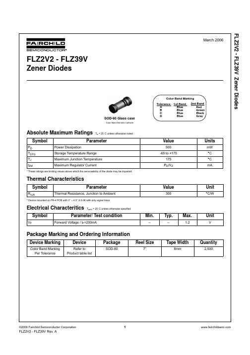
FLZ2V2 - FLZ39V Zener DiodesMarch 2006FLZ2V2 - FLZ39VZener DiodesAbsolute Maximum Ratings T a= 25°C unless otherwise noted* These ratings are limiting values above which the serviceability of the diode may be impaired.Thermal Characteristics* Device mounted on FR-4 PCB with 3’’ × 4.5” X 0.06 with only signal traceElectrical Characteritics Tamb = 25°C unless otherwise specifiedPackage Marking and Ordering InformationSymbolParameterValueUnitsP D Power Dissipation500mW T STG Storage Temperature Range -65 to +175°C T J Maximum Junction Temperature 175°C I ZMMaximum Regulator CurrentP D /V ZmASymbolParameterValueUnitR θJAThermal Resistance, Junction to Ambient300°C/WSymbolParameter/ Test conditionMin.Typ.Max.UnitV FForward Voltage / I F =200mA----1.2VDevice MarkingDevicePackageReel SizeTape WidthQuantityColor Band Marking Per ToleranceRefer to Product table listSOD-807”8mm2,500SOD-80 Glass caseColor Band Denotes CathodeColor Band MarkingTolerance 1st Band 2nd Band A Blue Red B Blue Green C Blue Black D Blue GrayFLZ3V0B 3.02 3.12 3.2135204501351 FLZ3V3FLZ3V3A 3.17 3.27 3.3635204501141 FLZ3V3B 3.33 3.43 3.5235204501141 FLZ3V6FLZ3V6A 3.48 3.57 3.6648208501 2.81 FLZ3V6B 3.64 3.73 3.8148208501 2.81 FLZ3V9FLZ3V9A 3.78 3.88 3.9740208501 1.41 FLZ3V9B 3.93 4.03 4.1240208501 1.41 FLZ4V3FLZ4V3A 4.07 4.15 4.23322085010.471 FLZ4V3B 4.22 4.30 4.38322085010.471FLZ4V3C 4.35 4.44 4.52322085010.471 FLZ4V7FLZ4V7A 4.48 4.56 4.64212077010.191 FLZ4V7B 4.60 4.68 4.75212077010.191FLZ4V7C 4.73 4.81 4.89212077010.191 FLZ5V1FLZ5V1A 4.86 4.94 5.021********.19 1.5 FLZ5V1B 4.99 5.08 5.16172068510.19 1.5FLZ5V1C 5.13 5.23 5.33172068510.19 1.5 FLZ5V6FLZ5V6A 5.31 5.41 5.5010.52042510.75 2.5 FLZ5V6B 5.48 5.58 5.6810.52042510.75 2.5FLZ5V6C 5.66 5.76 5.8610.52042510.75 2.5 FLZ6V2FLZ6V2A 5.83 5.94 6.048.5202551 3.33 FLZ6V2B 6.01 6.12 6.228.5202551 3.33FLZ6V2C 6.18 6.28 6.388.5202551 3.33 FLZ6V8FLZ6V8A 6.33 6.45 6.57 6.6201230.5 1.1 3.5 FLZ6V8B 6.54 6.66 6.77 6.6201230.5 1.1 3.5FLZ6V8C 6.72 6.83 6.93 6.6201230.5 1.1 3.5 FLZ7V5FLZ7V5A 6.907.047.17 6.620950.50.3 4.0 FLZ7V5B7.137.267.39 6.620950.50.3 4.0FLZ7V5C7.357.497.62 6.620950.50.3 4.0 FLZ8V2FLZ8V2A7.587.737.88 6.620950.50.35 FLZ8V2B7.847.998.13 6.620950.50.35FLZ8V2C8.098.248.39 6.620950.50.35 FLZ9V1FLZ9V1A8.348.518.68 6.620950.50.36 FLZ9V1B8.638.808.97 6.620950.50.36FLZ9V1C8.919.099.27 6.620950.50.36FLZ12VB11.5311.7111.899.510950.50.1339FLZ12VC11.8312.0512.279.510950.50.1339 FLZ13V FLZ13VA12.2112.4512.6811.410950.50.13310 FLZ13VB12.6212.8713.1211.410950.50.13310FLZ13VC13.0713.3315.3811.410950.50.13310 FLZ15V FLZ15VA13.5213.7914.0513.310950.50.13311 FLZ15VB13.9914.2614.5213.310950.50.13311FLZ15VC14.4514.7214.9913.310950.50.13311 FLZ16V FLZ16VA14.9015.1915.4715.2101320.50.13312 FLZ16VB15.3615.6515.9315.2101320.50.13312FLZ16VC15.8316.1416.4515.2101320.50.13312 FLZ18V FLZ18VA16.3816.7017.0219.4101230.50.13313 FLZ18VB16.9617.2917.6119.4101230.50.13313FLZ18VC17.5617.9018.2419.4101230.50.13313 FLZ20V FLZ20VA18.1718.5218.8623.5101700.50.13315 FLZ20VB18.7819.1319.4823.5101700.50.13315FLZ20VC19.4219.8020.1823.5101700.50.13315FLZ20VD19.9320.3020.6723.5101700.50.13315 FLZ22V FLZ22VA20.2820.6621.0325.651700.50.13317 FLZ22VB20.8221.2121.5925.651700.50.13317FLZ22VC21.2921.6622.0225.651700.50.13317FLZ22VD21.7522.1522.5425.651700.50.13317 FLZ24V FLZ24VA22.3222.6923.0629.051700.50.13319 FLZ24VB22.8123.2423.6729.051700.50.13319FLZ24VC23.3523.7824.2129.051700.50.13319FLZ24VD23.8724.3124.7529.051700.50.13319 FLZ27V FLZ27VA24.3324.8925.453852100.50.133 21 FLZ27VB25.0425.6226.193852100.50.133 21FLZ27VC25.6926.2926.883852100.50.133 21FLZ27VD26.3626.9727.573852100.50.133 21 FLZ30V FLZ30VA27.0727.6928.314652100.50.133 23 FLZ30VB27.7728.4129.054652100.50.133 23FLZ30VC28.4429.0929.744652100.50.133 23FLZ30VD29.1029.7730.434652100.50.133 23FLZ36VD34.1934.8935.596352100.50.13327 FLZ39V FLZ39VA34.8635.5736.287252100.50.13330 FLZ39VB35.5336.2636.997252100.50.13330FLZ39VC36.1836.9237.667252100.50.13330FLZ39VD36.8237.5838.337252100.50.13330Note :1. Zener Voltage(V z)The zener voltage is measured with the device junction in the thermal equilibrium at the lead temperature (TL) at at 30°C ± 1°C and 3/8” lead length.Dimensions in MillimetersFAIRCHILD SEMICONDUCTOR RESERVES THE RIGHT TO MAKE CHANGES WITHOUT FURTHER NOTICE TO ANY FAIRCHILD’S PRODUCTS ARE NOT AUTHORIZED FOR USE AS CRITICAL COMPONENTS IN LIFE SUPPORT DEVICES OR As used herein:2. A critical component is any component of a life support device Formative or In This datasheet contains the design specifications for This datasheet contains preliminary data, andThis datasheet contains final specifications. Fairchild This datasheet contains specifications on a product Across the board. Around the world.™DISCLAIMERPRODUCTS HEREIN TO IMPROVE RELIABILITY, FUNCTION OR DESIGN. FAIRCHILD DOES NOT ASSUME ANY LIABILITY ARISING OUT OF THE APPLICATION OR USE OF ANY PRODUCT OR CIRCUIT DESCRIBED HEREIN; NEITHER DOES IT CONVEY ANY LICENSE UNDER ITS PATENT RIGHTS, NOR THE RIGHTS OF OTHERS.LIFE SUPPORT POLICYSYSTEMS WITHOUT THE EXPRESS WRITTEN APPROVAL OF FAIRCHILD SEMICONDUCTOR CORPORATION.1. Life support devices or systems are devices or systems which, (a) are intended for surgical implant into the body, or (b) support or sustain life, or (c) whose failure to perform when properly used in accordance with instructions for use provided in the labeling, can be reasonably expected to result in significant injury to the user.or system whose failure to perform can be reasonably expected to cause the failure of the life support device or system, or to affect its safety or effectiveness.PRODUCT STATUS DEFINITIONS Definition of TermsDatasheet Identification Product Status DefinitionAdvance InformationDesign product development. Specifications may change in any manner without notice.PreliminaryFirst Productionsupplementary data will be published at a later date.Fairchild Semiconductor reserves the right to make changes at any time without notice in order to improve design.No Identification Needed Full ProductionSemiconductor reserves the right to make changes at any time without notice in order to improve design. Obsolete Not In Productionthat has been discontinued by Fairchild semiconductor.The datasheet is printed for reference information only.PACMAN™POP™Power247™PowerEdge™SPM™Stealth™SuperFET™SuperSOT™-3The Power Franchise ®Programmable Active Droop™Rev. I18。
鞍钢企业标准Q2752005
鞍山钢铁公司公司公司标准Q/ASB 275-2005取代 Q/ASB 275-2004汽车构造用热连轧钢板和钢带(SEW 092-82 , NEQ)2005-06-01 公布2005-06-01实行鞍山钢铁公司公司公布前言本标准依据热轧带钢厂1700 机组、 1780 机组生产汽车构造用钢板和钢带的实质状况,并联合市场的需求,对Q/ASB 275-2004 《汽车构造用热连轧钢板和钢带》进行订正。
本标准取代Q/ASB 275-2004 《汽车构造用热连轧钢板和钢带》。
本标准与Q/ASB 275-2004对比,主要变化以下:--汽车大梁用钢增添了A610L 牌号,汽车车轮用钢增添了A330LF、 A400LF 牌号;--增补了A610L、 A330LF、 A400LF 的化学成分和力学、工艺性能。
本标准的附录 A 是资料性附录。
本标准由鞍钢公司公司科技质量部提出。
本标准由鞍钢公司公司科技质量部归口。
本标准草拟单位:鞍钢公司公司科技质量部、鞍钢公司公司热轧带钢厂本标准主要草拟人:郑英杰、翟永彬本标准水同等级标记:Q/ASB 275-2005 Y。
本标准历次版本公布状况为:Q/ASB 275-1999 , Q/ASB 275-2003,Q/ASB 275-2004。
汽车构造用热连轧钢板和钢带1范围本标准规定了汽车构造用热连轧钢板和钢带的分类、订货内容、尺寸、外形、重量及同意误差、技术要求、试验方法、查验规则、包装、标记和质量证明书。
本标准合用于鞍钢公司公司热轧带钢厂生产的,拥有优秀冷成型性能的碳素钢、低合金及微合金钢热连轧钢板和钢带,产品用于制造汽车纵梁、横梁、滚型车轮、汽车桥壳等构造件及冲压件。
2规范性引用文件以下文件中的条款经过本标准的引用而成为本标准的条款。
凡是注日期的引用文件,其随后全部的改正单 ( 不包含勘误的内容 ) 或订正版均不合用于本标准,但是鼓舞依据本标准完成协议的各方研究能否可使用这些文件的最新版本。
VK3266
Viken 01/2007
VK3266数据手册 Ver0.12
维肯电子 2006年 发布 版权所有
1 of 29
维肯电子
VK3266
SPI/UART/8位并行总线接口 宽工作电压 4通道 16级FIFO的UART
维肯电子
VK3266
SPI/UART/8位并行总线接口 宽工作电压 4通道 16级FIFO的UART
VK3266 多总线接口 四通道通用异步收发器 无铅封装
1.产品概述
VK3266是业界首款具备 UART/SPITM/8位并行总线接口的4通道UART器件。可以通过模式选择使得 该芯片工作于以上任何一种主接口模式下:
6.1封装图
Viken 01/2007
VK3266数据手册 Ver0.12
维肯电子 2006年 发布 版权所有
3 of 29
维肯电子
VK3266
SPI/UART/8位并行总线接口 宽工作电压 4通道 16级FIFO的UART
44 GND 43 OSCI 42 OSCO 41 CLKSEL 40 CLKIN 39 VCC 38 RTS3 37 RX3 36 TX3 35 CTS3 34 RTS1
2.4 SPI主接口特性
最高速度5M bit/s 仅支持SPI从模式 16位,SPI模式0
2.5 8位并口主接口特性
标准8位MCU总线接口 命令和数据共用8位地址总线,通过A0(数据/控制)信号进行切换 子通道选择通过命令字控制和指示,无需额外的通道指示信号线 仅占用2个地址空间
3.应用领域
多串口服务器/多串口卡 工业/自动化现场RS-485控制 通过CDMA/GPRS MODEM的无线数据传输 车载信息平台/车载GPS定位系统 远传自动抄表(AMR)系统 POS/税控POS/金融机具 DSP/嵌入式系统
西门子变频器手册
应用实例手册西门子通用变频器应用实例前 言西门子通用变频器应用实例手册经过标准传动部同事和合作伙伴的共同努力和支持下将与广大读者见面。
具有153年悠久历史的德国西门子公司作为变频调速,尤其是矢量控制技术的发明者和领导者,开发和生产变频器已有近30年历史。
在全世界以及中国,无论是冶金,水泥,机械等重工业,或者是在编织化纤,食品饮料,楼宇建筑等其他行业,西门子变频技术都得到了广泛应用。
此手册中详尽描述了西门子通用变频器在各个行业领域中的应用。
我们的出发点是通过这些应用实例为您提供一些技术指导,普及和推广西门子通用变频器在行业中的应用,为您的企业带来更大的经济效益。
此手册中的文章均来自现场的应用实例,由于各个现场应用情况差异较大,还有许多不完善之处,在此仅供您参考,如果想了解更多详情,欢迎您与我们联系,我们将尽力为您服务。
由于时间有限,编辑的不当之处,在所难免,还请广大读者给予指正和谅解。
随着西门子通用变频器应用实例的不断增多,我们热忱的希望您能提出宝贵建议,在您的鼓励和帮助下,我们会使此手册不断的丰富和完善起来。
我们同时也欢迎您一起来与我们共同分享您在应用西门子变频器中的体会。
最后,再次感谢给予此手册大力支持和帮助的个位同事和合作伙伴。
西门子标准传动部张登山肖芳2002.11西门子通用变频器应用实例广州信心电子有限公司MM440变频调速系统在空压机系统上的应用 (3)ECO变频调速系统在中央空调系统上的应用 (4)北京大恒电气有限责任公司MM440变频器在港务局水泥码头上的应用 (8)ECO变频器在电厂加热网疏水泵上的应用 (9)上海大华电脑电器公司变频器在起重机大、小车行走驱动中的应用 (11)6SE92变频器在化纤加弹机上的应用 (14)河南怡和电气自动化电气有限公司ECO变频器在高新技术产业开发区热力公司锅炉恒压/恒液位供水系统上的应用 (16)MDV 变频器在车辆段铁车辆段空气压缩机上的应用 (18)凯德实业有限公司MICROMASTER440变频器在啤酒瓶传送生产线上的应用 (19)MICROMASTER440变频器在啤酒厂水处理线上的应用 (20)北京进步时代科技有限公司MM440通用变频器在位置控制中的应用 (22)变频调速在螺纹钢生产线上的应用 (24)瑞能电气有限公司MM440变频器在石油管理局给水工程公司水表厂水表自动化检测校验系统 (27)MICROMASTER440变频器在重型机械制造厂密度板联动生产线上的应用 (29)西门子自动化与驱动集团标准传动部西门子新一代MM440变频器在电梯上的运用 (31)MM420变频器在纺织行业细纱机上的运用 (33)MM440 在工业洗衣机上的应用 (36)MM440变频器在造纸机传动控制系统的应用 (38)HVAC 楼宇暖通空调应用实例 ECO变频器在中国银行大厦中的应用 (39)山东韦尔斯电器有限公司MM420变频器在编织机上的应用 (41)MM420变频器在黄河水文测验电动吊箱上的应用 (43)南京航大意航科技股份有限公司MM420在给水系统的几点节能措施 (44)重庆市凌集科技有限责任公司MM440变频调速系统在铣床上的应用 (46)西门子通用变频器应用实例MM440变频调速系统在空压机系统上的应用— 广州信心电子有限公司一系统概述在大型化工厂的能量损耗中,大功率空压机系统的电能损耗占据了一个很大的比例。
AP1512-33N中文资料

AP1512/A50KHz, 2A/3A PWM Buck DC/DC ConverterFeatures- Output voltage: 3.3V, 5V, 12V and adjustable output version- Adjustable version output voltage range, 1.23V to 37V+4%- 50KHz +15% fixed switching frequency- Voltage mode non-synchronous PWM control - Thermal-shutdown and current-limit protection - ON/OFF shutdown control input - Operating voltage can be up to 60V - Output load current: 2A (for AP1512)3A (for AP1512A)- Low power standby mode- Built-in switching transistor on chip - TO220-5L, TO220-5L(R) and TO263-5L Pb-free packagesApplications- Simple High-efficiency step-down regulator - On-card switching regulators - Positive to negative converterGeneral DescriptionThe AP1512/A is a monolithic IC that design for a step-down DC/DC converter, and own the ability of driving a 2A (3A for AP1512A) load without additional transistor component. Due to reducing the number of external component, the board space can be saved easily. The external shutdown function can be controlled by logic level and then come into standby mode. The internal compensation makes feedback control have good line and load regulation without external design. Regarding protected function, thermal shutdown is to prevent over temperature operating from damage, and current limit is against over current operating of the output switch. The AP1512/A operates at a switching frequency of 50KHz thus allowing smaller sized filter components than what would be needed with lower frequency switching regulators. Other features include a guaranteed +4% tolerance on output voltage under specified input voltage and output load conditions, and +15% on the oscillator frequency. The output version included fixed 3.3V, 5V, 12V, and an adjustable type. The packages are available in a standard 5-lead TO-220 package and a 5-lead TO-263.Pin AssignmentsTO220-5L( Top View )( Top View )TO263-5L INMetal Tab GNDINPin DescriptionsNameDescriptionV IN Operating voltage input Output Switching output Gnd Ground FBOutput voltage feedback controlSD ON/OFF ShutdownAP1512/A50KHz, 2A/3A PWM Buck DC/DC ConverterOrdering InformationPackage T5: TO220-5LK5: TO263-5LOutput Version AP1512 X XX X XPacking Blank : Tube A : TapingBlank : Adjustable -33 : 3.3V -50 : 5.0V -12 : 12VT5R: TO220-5L(R)Part Number Blank: 2A A : 3ABlock DiagramCurrent Source bias1.235V Reference2.5V Regulator50KHz OSC.Start up++_+_Thermal LimitPre-driverComp CompGndOutput V INSDFB220mV200mV2A Switch +__Amp CompFrequecy compen-sation(3A for AP1512A)AP1512/A50KHz, 2A/3A PWM Buck DC/DC ConverterAbsolute Maximum RatingsSymbol Parameter RatingUnit V CC Supply Voltage +63 V V SD ON/OFF Pin input voltage -0.3 to +40 V V FB Feedback Pin voltage -0.3 to +40V V OUT Output voltage to Ground -1V P D Power dissipation Internally limited W T ST Storage temperature -65 to +150 o C T OP Operating temperature -40 to +125 o C V OP Operating voltage+4.5 to +60VElectrical Characteristics (All Output Voltage Versions)Unless otherwise specified, V IN =30V for all version. I LOAD = 0.5ASymbol ParameterConditionsMin.Typ.Max. Unit 8I BFeedback bias currentV FB =1.3V(Adjustable version only)5 10µA42.5 50 57.5F OSC oscillator frequency40 60KHz1.4V SAT saturation voltage I OUT =2A no outside circuitV FB =0V force driver on1.3 1.5VMax. Duty Cycle(ON) V FB =0V force driver on100DCMin. Duty cycle(OFF) V FB =12V force driver off%4.5I CL current limit for AP1512 peak currentno outside circuitV FB =0V force driver on 2.5 3 5.5A5I CL current limit for AP1512A peak current no outside circuitV FB =0V force driver on3.2 4 6 A Output = 0no outside circuitV FB =12V force driver off-250 uA I L Output = -1 Output leakage currentV IN =60V -2 -60 mA I Q Quiescent Current V FB =12V force driver off 5 10 mA450 I STBYStandby Quiescent Current ON/OFF pin=5VV IN =60V 350 500uA V IL Low (regulator ON) - 0.6 V IH ON/OFF pin logic inputthreshold voltage High (regulator OFF) 2.0 1.3 - VI H ON/OFF pin logic input currentV LOGIC =2.5V (OFF) 0 -5I L ON/OFF pin input current V LOGIC =0.5V (ON) -0.8 -10uA TO220-5L 2.5 θJC Thermal Resistance TO263-5L Junction to case3.5 oC/WTO220-5L 28 θJA Thermal ResistanceWith copper area ofapproximately 3 in 2TO263-5L Junction to ambient 23 oC/WAP1512/A50KHz, 2A/3A PWM Buck DC/DC ConverterElectrical Characteristics (Continued)AP1512Symbol Parameter Conditions Typ. Limit Unit AP1512-ADJ FB V Output Feedback 10V < V IN < 60V 0.2A < I LOAD < 2AV OUT programmed for 3V 1.231.193/1.18 1.267/1.28 V V MIN V MAX AP1512-3.3V OUT V Output voltage 10V < V IN < 60V 0.2A < I LOAD < 2A 3.3 3.168/3.135 3.432/3.465 V V MIN V MAX AP1512-5VOUT V Output voltage 10V < V IN < 60V 0.2A < I LOAD < 2A 5 4.8/4.75 5.2/5.25 V V MIN V MAX OUT V Output voltage15V < V IN < 60V 0.2A < I LOAD < 2A12 11.52/11.4 12.48/12.6V V MIN V MAX AP1512-12VηEfficiency V IN = 30V, I LOAD = 2A 83 % AP1512ASymbol Parameter Conditions Typ. Limit Unit AP1512A-ADJ FB V Output Feedback 10V < V IN < 60V 0.2A < I LOADV OUT programmed for 3V 1.231.193/1.18 1.267/1.28 V V MIN V MAX AP1512A-3.3V OUT V Output voltage 10V < V IN < 60V 0.2A < I LOAD 3.3 3.168/3.135 3.432/3.465 V V MIN V MAX AP1512A-5VOUT VOutput voltage10V < V IN < 60V 0.2A < I LOAD54.8/4.755.2/5.25V V MIN V MAX OUT V Output voltage15V < V IN < 60V 0.2A < I LOAD12 11.52/11.4 12.48/12.6V V MIN V MAX AP1512A-12VηEfficiency V IN = 30V, I LOAD = 3A80%Specifications with boldface type are for full operating temperature range, the other type are for T J =25ºC.Typical Performance CharacteristicsAP1512A Current Limit v.s. Temperature(Vcc=60V, Vout=5V)33.23.43.63.84-50050100150Temperature (TA) (°C)C u r r e n t L i m i t (A )AP1512A Efficiency v.s. Supply Voltage(Vout=5V, Iout=3A)10203040506070809010001224364860Supply Voltage(V)E f f i c i e n c y (%)AP1512/A50KHz, 2A/3A PWM Buck DC/DC ConverterTypical Performance Characteristics (Continued)AP1512 Efficiency v.s. Temperature(Vin=12V,Vout=5V,Io=2A)102030405060708090100-50-30-101030507090*********Temperature (TA) (°C)E f f i c i e n c y (%)AP1512 Efficiency v.s. Temperature(Vin=12V,Vout=3.3V,Io=2A)102030405060708090100-50-30-101030507090*********Temperature (TA) (°C)E f f i c i e n c y (%)AP1512 Supply Current v.s. Temperature(Vcc=12V , No Load ,Von/off =0V(Switch ON) ,Von/off =5V(Switch OFF))12345678-40-25-105203550658095110125S u p p l y C u r r e n t (m A )Temperature (TA) (°C)Switch ON102030405060708090100-40-25-105203550658095110125S u p p l y C u r r e n t (u A )Temperature (TA) (°C)Switch OFFAP1512 Output Voltage v.s. Temperature(Vin=12V, Vout=5V, Io=1A)4.704.754.804.854.904.955.005.055.10-50050100150O u t p u t V o l t a g e (V )Temperature (TA) (°C)AP1512 Threshold Voltage v.s. Temperature(Vcc=12V, Vout=5V)00.20.40.60.811.21.41.6-50050100150T h r e s h o l d V o l t a g e (V )Temperature (TA) (°C)AP1512/A50KHz, 2A/3A PWM Buck DC/DC ConverterTypical Performance Characteristics (Continued)AP1512 Frequency v.s. Temperature(Vcc=12V, Io=1A, Vout=5V)4045505560-50-30-101030507090110130150Temperature (TA) (°C)F r e q u e n c y (K H z )AP1512 Current Limit v.s. Temperature(Vcc=60V, Vout=5V)2.833.23.43.6-5050100150C u r r e n t L i m i t (A )Temperature (TA) (°AP1512 Quiescent Current v.s. Supply Voltage(force driver off)5.25.45.65.866.21224364860Q u i e s c e n t C u r r e n t (A )Supply Voltage(V)AP1512/A50KHz, 2A/3A PWM Buck DC/DC ConverterTypical Application Circuit(1) Adjustable Type CircuitA. Vin=10V~60V, Vout=5V; Iout=0.3A~2A, Iout below 0.3A DCMC51nL147uH12R23KVinC21uD1SR360ON/OFFR31KC1100uF/100VAP1512/A15243VinSDOUTPUTFBGND 0.1uC3470uF/16VC7B. Vin=10V~60V, Vout=3.3V, Iout=0.3A~2A, Iout below 0.3A DCMC51nL147uH12R22KVinC21uD1SR360ON/OFFR31.2KC1100uF/100VAP1512/A15243VinSDOUTPUTFBGND 0.1uC3470uF/16VC7(2) Fixed Type CircuitA. Vin=10V~60V, Vout=5V, Iout=0.7A~2A, Iout below 0.7A DCML147uH12VinC21uD1SR360ON/OFFC1100uF/100VVoutAP1512/A15243VinSDOUTPUTFBGND 10nC3470uF/16VC7AP1512/A50KHz, 2A/3A PWM Buck DC/DC ConverterTypical Application Circuit (Continued)B. Vin=10V~60V, Vout=3.3V, Iout=0.7A~2A, Iout below 0.7A DCML133uH12VinC23.3uD1SR360ON/OFFC1220uF/100VVoutAP1512/A15243VinSDOUTPUTFBGND 3.3uC31500uF/16VC7Function Description+V INThis is the positive input supply for the IC switching regulator. A suitable input bypass capacitor must be present at this pin to minimize voltage transients and to supply the switching currents needed by the regulator.GroundCircuit ground.OutputInternal switch. The voltage at this pin switches between (+V IN – V SAT ) and approximately – 0.5V, with a duty cycle of approximately V OUT / V IN . To minimize coupling to sensitive circuitry, the PC board copper area connected to this pin should be kept a minimum.FeedbackSenses the regulated output voltage to complete the feedback loop.ON /OFFAllows the switching regulator circuit to be shutdown using logic level signals thus dropping the total input supply current to approximately 150uA. Pulling this pin below a threshold voltage of approximately 1.3V turns the regulator on, and pulling this pin above 1.3V (up to a maximum of 40V) shuts the regulator down. If this shutdown feature is not needed, the SD pin can be wired to the ground pin or it can be left open, in either case the regulator will be in the ON condition.Thermal ConsiderationsThe AP1512/A is available in two packages, a 5-pin TO-220 and a 5-pin surface mount TO-263.The TO-220 package needs a heat sink under most conditions. The size of the heatsink depends on the input voltage, the output voltage, the load current and the ambient temperature. The AP1512/A junction temperature rises above ambient temperature for a 2A load and different input and output voltages. The data for these curves was taken with the AP1512/A (TO-220 package) operating as a buckswitching regulator in an ambient temperature of 25o C (still air). These temperature rise numbers are all approximate and there are many factors that can affect these temperatures. Higher ambient temperatures require more heat sinking.The TO-263 surface mount package tab is designed to be soldered to the copper on a printed circuit board. The copper and the board are the heat sink for this package and the other heat producing components, such as the catch diode and inductor. The PC board copper area that the package is soldered to should be at least 0.4 in 2, and ideally should have 2 or more square inches of 2 oz. Additional copper area improves the thermal characteristics, but with copper areas greater than approximately 6 in 2, only small improvements in heat dissipation are realized. If further thermal improvements are needed, double sided, multilayer PC board with large copper areas and/or airflow are recommended.AP1512/A50KHz, 2A/3A PWM Buck DC/DC ConverterFunction Description (Continued)The AP1512/A (TO-263 package) junction temperature rise above ambient temperature with a 2A load for various input and output voltages. This data was taken with the circuit operating as a buck switching regulator with all components mounted on a PC board to simulate the junction temperature under actual operating conditions. This curve can be used for a quick check for the approximate junction temperature for various conditions, but be aware that there are many factors that can affect the junction temperature. When load currents higher than 2A are used, double sided or multilayer PC boards with large copper areas and/or airflow might be needed, especially for high ambient temperatures and high output voltages.For the best thermal performance, wide copper traces and generous amounts of printed circuit board copper should be used in the board layout. (Once exception to this is the output (switch) pin, which should not have large areas of copper.) Large areas of copper provide the best transfer of heat (lower thermal resistance) to the surrounding air, and moving air lowers the thermal resistance even further.Package thermal resistance and junction temperature rise numbers are all approximate, and there are many factors that will affect these numbers. Some of these factors include board size, shape, thickness, position, location, and even board temperature. Other factors are, trace width, total printed circuit copper area, copper thickness, single or double-sided, multilayer board and the amount of solder on the board. The effectiveness of the PC board to dissipate heat also depends on the size, quantity and spacing of other components on the board, as well as whether the surrounding air is still or moving. Furthermore, some of these components such as the catch diode will add heat to the PC board and the heat can vary as the input voltage changes. For the inductor, depending on the physical size, type of core material and the DC resistance, it could either act as a heat sink taking heat away from the board, or it could add heat to the board.Marking Information(1) TO263-5L1512X-XX Blank: ADJ ( Top View )"02" = 2002"01" = 2001YY WW X01~52~Part Number:A: AP1512A(2) TO220-5L1512X-XX ID codeYear:"02" = 2002"01" = 2001YY WW XXth week:01~52~Blank: ADJ LogoPart Number:-Output Type: -33: 3.3V -50: 5.0V -12: 1.2V Blank: AP1512A: AP1512AAP1512/A 50KHz, 2A/3A PWM Buck DC/DC ConverterPackage Information(1) Package Type: TO220-5LD QEbe1AJ1FCΦPH1LeDimensions In Millimeters Dimensions In InchesSymbolMin. Nom. Max. Min. Nom. Max.A 4.07 4.45 4.82 0.160 0.175 0.190b 0.76 0.89 1.02 0.030 0.035 0.040C 0.36 0.50 0.64 0.014 0.020 0.025D 14.22 14.86 15.50 0.560 0.585 0.610E 9.78 10.16 10.54 0.385 0.400 0.415e 1.57 1.71 1.85 0.062 0.067 0.073e1 6.68 6.81 6.93 0.263 0.268 0.273F 1.14 1.27 1.40 0.045 0.050 0.055H1 5.46 6.16 6.86 0.215 0.243 0.270 J1 2.29 2.74 3.18 0.090 0.108 0.125 L 13.21 13.97 14.73 0.520 0.550 0.580 Øp 3.68 3.81 3.94 0.145 0.150 0.155 Q 2.54 2.73 2.92 0.100 0.107 0.115AP1512/A 50KHz, 2A/3A PWM Buck DC/DC ConverterPackage Information (Continued)(2) Package Type: TO263-5LEL2e B DLAC2CL11.02.515.710.99.11.7Land Pattern Recommendation (Unit: mm)Dimensions In Millimeters Dimensions In InchesSymbolMin. Nom. Max. Min. Nom. Max.A 4.07 4.46 4.85 0.160 0.176 0.191B 0.66 0.84 1.02 0.026 0.033 0.040C 0.36 0.50 0.64 0.014 0.020 0.025C2 1.14 1.27 1.40 0.045 0.050 0.055D 8.65 9.15 9.65 0.341 0.360 0.380E 9.78 10.16 10.54 0.385 0.400 0.415e 1.57 1.71 1.85 0.062 0.068 0.073L 14.61 15.24 15.88 0.575 0.600 0.625 L1 2.29 2.54 2.79 0.090 0.100 0.110 L2 - - 2.92 - - 0.115AP1512/A50KHz, 2A/3A PWM Buck DC/DC ConverterPackage Information (Continued)(3) Package Type: TO220-5L(R) Mechanical drawingEQDbAFH1d1d2J3J1J2eH2H3AJ1J2J3EDimensions In Millimeters Dimensions In Inches SymbolMin. Nom. Max. Min. Nom. Max.A 4.4 4.6 4.7 0.175 0.180 0.185b 0.7 0.8 0.9 0.027 0.032 0.037 D 8.4 8.7 8.9 0.330 0.340 0.350 d1 1.0 0.039 d2 6.3 0.248 E 9.91 10.16 10.41 0.390 0.400 0.410 e 1.6 1.7 1.8 0.062 0.067 0.072 F 1.2 1.25 1.3 0.048 0.050 0.052 H1 6.4 0.250 H2 20.8 21.6 22.4 0.820 0.850 0.880 H3 23.9 24.7 25.5 0.942 0.972 1.002 J1 2.7 0.105 J2 3.7 4.5 5.3 0.147 0.177 0.207 J3 8.4 0.331 Q 2.5 2.8 3.0 0.100 0.110 0.120。
SL33资料

SL32 THRU SL34LOW VF SURFACE MOUNT SCHOTTKY BARRIER RECTIFIERVOLTAGE - 20 to 40 Volts CURRENT - 3.0 AmperesFEATURESl Plastic package has Underwriters Laboratory Flammability Classification 94V-O l For surface mounted applications l Low profile package l Built-in strain relief l Metal to silicon rectifier majority carrier conductionl Low power loss, High efficiency l High current capability, low V Fl High surge capacityl For use in low voltage high frequency inverters, free wheeling, and polarity protection applications l High temperature soldering guaranteed: 260¢J /10 seconds at terminals MECHANICAL DA TACase: JEDEC DO-214AB molded plasticTerminals: Solder plated, solderable per MIL-STD-750, Method 2026Polarity: Color band denotes cathodeStandard packaging: 16mm tape (EIA-481)Weight: 0.007 ounce, 0.21 gramMAXIMUM RA TINGS AND ELECTRICAL CHARACTERISTICSRatings at 25¢J ambient temperature unless otherwise specified.Resistive or inductive load.SYMBOLS SL32SL33SL34UNITS Maximum Recurrent Peak Reverse Voltage V RRM 203040Volts Maximum RMS Voltage V RMS 142128Volts Maximum DC Blocking Voltage V DC 203040VoltsMaximum Average Forward Rectified Current at T L (See Figure 1)I (AV) 3.0Amps Peak Forward Surge Current 8.3ms single half sine-wave superimposed on rated load(JEDEC method)I FSM100.0Amps Maximum Instantaneous Forward Voltage at 3.0A (Note 1)V F 0.380.380.40Volts Maximum DC Reverse Current T A =25¢J (Note 1)At Rated DC Blocking Voltage T A =100¢J I R 0.520.0mA Maximum Thermal Resistance (Note 2)R £K JLR £K JA1755¢J /W Operating Junction Temperature Range T J -50 to +125¢J Storage Temperature Range T STG -50 to +150¢JNOTES:1. Pulse Test with PW=300£g s, 1% Duty Cycle.2. Mounted on P.C.Board with 14mm 2(.013mm thick) copper pad areas.S MC/DO-214ABRATING AND CHARACTERISTIC CURVES SL32 THRU SL34LEAD TEMPERATURE,¢JTYPICAL INSTANTANEOUS FORWARD CHARACTERISTICSFig. 1-FORWARD CURRENT DERATING CURVE Fig. 2-TYPICAL INSTANTANEOUS FORWARDCHARACTERISTICSREVERSE VOLTAGE. VOLTSFig. 4-TYPICAL JUNCTION CAPACITANCEPERCENT OF RATED PEAK REVERSE VOLTAGEFig. 3-TYPICAL REVERSE CHARACTERISTICSNUMBER OF CYCLES AT 60HzFig. 5-MAXIMUM NON-REPETITIVE PEAK FORWARDSURGE CURRENT。
CS5530中文资料
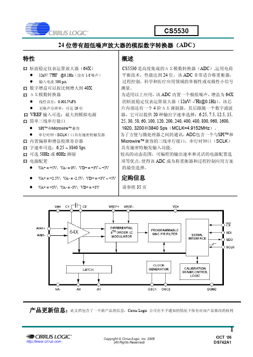
特性
概述
口 斩波稳定仪表运算放大器(64X)
z 12nV/√Hz @0.1Hz(没有 1/f 噪声) z 输入电流 500 pA
口 数字增益可以按比例增大到 40X 口 ΔΣ模数转换器
z 线性误差:0.0015%FS z 无噪声分辨率:可达 19 位
附表
表 1. 单次模式的转换时间……………………………………………………………………….……………24 表 2. 连续模式的转换时间…………………………………………………………………………………….24 表 3. 输出编码………………………………………………………………………………………………….25
口 VREF 输入可选:最大到模拟电源 口 简单三线串行接口
z SPI™和Microwire™兼容 z 串行时钟(SCLK)口具有施密特触发器
口 内置偏移和增益校准寄存器 口 字速率可选:6.25 ~ 3840 Sps 口 可选 50Hz 或 60Hz 抑制 口 电源配置
z VA+ = +5V;VA- = 0V;VD+ = +3V ~ +5V
25, 30, 50, 60, 100, 120, 200, 240, 400, 480, 800, 960, 1600, 1920, 3200和3840 Sps(MCLK=4.9152MHz)。 为了方便与微处理器之间的通讯,ADC包含一个与SPI™和 Microwire™兼容的三线串行接口,串行时钟口(SCLK) 具有施密特触发输入功能。 较高的动态范围,可编程的输出速率和灵活的电源配置选 项等优点,使得该 ADC 成为称重衡器和过程控制应用方案 的最佳选择。
SMBJ6.0CA中文资料

SMBJ5.0(C)A - SMBJ440(C)A600W Surface Mount Transient Voltage SuppressorFeatures600W Peak Pulse Power Dissipation5.0V - 440V Standoff VoltagesGlass Passivated Die ConstructionUni- and Bi-Directional Versions AvailableExcellent Clamping CapabilityFast Response TimePlastic Material - UL FlammabilityClassification Rating 94V-0Mechanical DataCase: SMB, Transfer Molded EpoxyTerminals: Solderable per MIL-STD-202,Method 208Polarity Indicator: Cathode Band(Note: Bi-directional devices have no polarityindicator.)Marking: Date Code and Marking CodeSee Page 2Weight: 0.1 grams (approx.)MAXIMUM RATINGSRating at T a = 25 C ambient temperature unless otherwise specified.DO-214AA (SMB)0.083(2.11) 0.155(3.94) 0.075(1.91) 0.130(3.30)0.185(4.70)0.160(4.06)0.012(0.31)0.006(0.15) 0.096(2.44)0.083(2.13)0.050(1.27) 0.008(0.203)0.030(0.76) MAX.0.220(5.59)0.200(5.08)Dimensions in inches and (millimeters)Rating Symbol Value Units Peak Pulse Power Dissipation on 10/1000μs (1)waveform (Notes 1, 2, Fig. 3) P PPM Minimum 600 Watts Peak Pulse Current on 10/1000μswaveform (Note 1, Fig. 5) I PPM See T able Amps Peak forward Surge Current8.3 ms single half sine-wave superimposed onrated load ( JEDEC Method )(Notes 2, 3)Maximum Instantaneous Forward Voltage at 50A V FM See Note 3, 4 Volts Operating Junction and Storage T emperature Range T J, T STG - 65 to + 150 CNote :(1) Non-repetitive Current pulse, per Fig. 5 and derated above Ta = 25 C per Fig. 1(2) Mounted on 5.0mm2 (0.013mm thick) land areas.(3) Measured on 8.3ms. Single half sine-wave or equivalent square wave, duty cycle = 4 pulses per minutes maximum.SMBJ6.0CATYPE MarkingReverse BreakdownStand-Off VoltageVoltage Min. @I TBreakdownVoltage TestMax. @ I T CurrentMaximumClampingVoltage@I PPPeak ReversePulse LeakageCurrent @V RMW(Uni) (BI) (Uni) (Bi) V RMW (V) V BR MIN(V) V BR MAX(V) I T (mA) V C(V) I PP(A) I R(uA) SMBJ5.0 SMBJ5.0C KD AD 5.0 6.40 7.55 10 9.6 62.5 800.0 SMBJ5.0A SMBJ5.0CA KE AE 5.0 6.40 7.25 10 9.2 65.2 800.0 SMBJ6.0 SMBJ6.0C KF AF 6.0 6.67 8.45 10 11.4 52.6 800.0 SMBJ6.0A SMBJ6.0CA KG AG 6.0 6.67 7.67 10 10.3 58.3 800.0 SMBJ6.5 SMBJ6.5C KH AH 6.5 7.22 9.14 10 12.3 48.8 500.0 SMBJ6.5A SMBJ6.5CA KK AK 6.5 7.22 8.30 10 11.2 53.6 500.0 SMBJ7.0 SMBJ7.0C KL AL 7.0 7.78 9.86 10 13.3 45.1 200.0 SMBJ7.0A SMBJ7.0CA KM AM 7.0 7.78 8.95 10 12.0 50.0 200.0 SMBJ7.5 SMBJ7.5C KN AN 7.5 8.33 10.67 1.0 14.3 42.0 100.0 SMBJ7.5A SMBJ7.5CA KP AP 7.5 8.33 9.58 1.0 12.9 46.5 100.0 SMBJ8.0 SMBJ8.0C KQ AQ 8.0 8.89 11.3 1.0 15.0 40.0 50.0 SMBJ8.0A SMBJ8.0CA KR AR 8.0 8.89 10.23 1.0 13.6 44.1 50.0 SMBJ8.5 SMBJ8.5C KS AS 8.5 9.44 11.92 1.0 15.9 37.7 20.0 SMBJ8.5A SMBJ8.5CA KT AT 8.5 9.44 10.82 1.0 14.4 41.7 20.0 SMBJ9.0 SMBJ9.0C KU AU 9.0 10.0 12.6 1.0 16.9 35.5 10.0 SMBJ9.0A SMBJ9.0CA KV AV 9.0 10.0 11.5 1.0 15.4 39.0 10.0 SMBJ10 SMBJ10C KW AW 10 11.1 14.1 1.0 18.8 31.9 5.0 SMBJ10A SMBJ10CA KX AX 10 11.1 12.8 1.0 17.0 35.3 5.0 SMBJ11 SMBJ11C KY AY 11 12.2 15.4 1.0 20.1 29.9 5.0 SMBJ11A SMBJ11CA KZ AZ 11 12.2 14.0 1.0 18.2 33.0 5.0 SMBJ12 SMBJ12C LD BD 12 13.3 16.9 1.0 22.0 27.3 5.0 SMBJ12A SMBJ12CA LE BE 12 13.3 15.3 1.0 19.9 30.2 5.0 SMBJ13 SMBJ13C LF BF 13 14.4 18.2 1.0 23.8 25.2 5.0 SMBJ13A SMBJ13CA LG BG 13 14.4 16.5 1.0 21.5 27.9 5.0 SMBJ14 SMBJ14C LH BH 14 15.6 19.8 1.0 25.8 23.3 5.0 SMBJ14A SMBJ14CA LK BK 14 15.6 17.9 1.0 23.2 25.9 5.0 SMBJ15 SMBJ15C LL BL 15 16.7 21.1 1.0 26.9 22.3 5.0 SMBJ15A SMBJ15CA LM BM 15 16.7 19.2 1.0 24.4 24.6 5.0 SMBJ16 SMBJ16C LN BN 16 17.8 22.6 1.0 28.8 20.8 5.0 SMBJ16A SMBJ16CA LP BP 16 17.8 20.5 1.0 26.0 23.1 5.0 SMBJ17 SMBJ17C LQ BQ 17 18.9 23.9 1.0 30.5 19.7 5.0 SMBJ17A SMBJ17CA LR BR 17 18.9 21.7 1.0 27.6 21.7 5.0 SMBJ18 SMBJ18C LS BS 18 20.0 25.3 1.0 32.2 18.6 5.0 SMBJ18A SMBJ18CA LT BT 18 20.0 23.3 1.0 29.2 20.5 5.0 SMBJ20 SMBJ20C LU BU 20 22.2 28.1 1.0 35.8 16.8 5.0 SMBJ20A SMBJ20CA LV BV 20 22.2 25.5 1.0 32.4 18.5 5.0 SMBJ22 SMBJ22C LW BW 22 24.4 30.9 1.0 39.4 15.2 5.0 SMBJ22A SMBJ22CA LX BX 22 24.4 28.0 1.0 35.5 16.9 5.0 SMBJ24 SMBJ24C LY BY 24 26.7 33.8 1.0 43.0 14.0 5.0 SMBJ24A SMBJ24CA LZ BZ 24 26.7 30.7 1.0 38.9 15.4 5.0 SMBJ26 SMBJ26C MD CD 26 28.9 36.6 1.0 46.6 12.9 5.0 SMBJ26A SMBJ26CA ME CE 26 28.9 33.2 1.0 42.1 14.3 5.0 SMBJ28 SMBJ28C MF CF 28 31.1 39.4 1.0 50.0 12.0 5.0 SMBJ28A SMBJ28CA MG CG 28 31.1 35.8 1.0 45.4 13.2 5.0 Note:( 1 ) V BR measured after I T applied for 300 s., I T = square wave pulse or equivalent. ( 2 )Surge Current Waveform per Figure 5 and Derate per Figure 1( 3 ) A Transient suppressor is normally selected according to the reverse " Stand-off Voltage " (V WM) which should beequal to or greater then the D.C. or continuous peak operating voltage level.SMBJ6.0CAReverse Breakdown Breakdown Maximum Peak Reverse TYPE Marking Stand-Off Voltage Voltage Test Clamping Pulse LeakageVoltage Min. @I T Max. @ I T Current Voltage @I PP Current @V RMW (Uni) (BI) (Uni) (Bi) V RMW (V) V BR MIN(V) V BR MAX(V) I T (mA) V C(V) I PP(A) I R(uA) SMBJ30 SMBJ30C MH CH 30 33.3 42.2 1.0 53.5 11.2 5.0 SMBJ30A SMBJ30CA MK CK 30 33.3 38.3 1.0 48.4 12.4 5.0 SMBJ33 SMBJ33C ML CL 33 36.7 46.5 1.0 59.0 10.2 5.0 SMBJ33A SMBJ33CA MM CM 33 36.7 42.2 1.0 53.3 11.3 5.0 SMBJ36 SMBJ36C MN CN 36 40.0 50.7 1.0 64.3 9.3 5.0 SMBJ36A SMBJ36CA MP CP 36 40.0 46.0 1.0 58.1 10.3 5.0 SMBJ40 SMBJ40C MQ CQ 40 44.4 56.3 1.0 71.4 8.4 5.0 SMBJ40A SMBJ40CA MR CR 40 44.4 51.1 1.0 64.5 9.3 5.0 SMBJ43A SMBJ43CA MT CT 43 47.8 54.9 1.0 69.4 8.6 5.0 SMBJ45 SMBJ45C MU CU 45 50.0 63.3 1.0 80.3 7.5 5.0 SMBJ45A SMBJ45CA MV CV 45 50.0 57.5 1.0 72.7 8.3 5.0 SMBJ48 SMBJ48C MW CW 48 53.3 67.5 1.0 85.5 7.0 5.0 SMBJ48A SMBJ48CA MX CX 48 53.3 61.3 1.0 77.4 7.8 5.0 SMBJ51 SMBJ51C MY CY 51 56.7 71.8 1.0 91.1 6.6 5.0 SMBJ51A SMBJ51CA MZ CZ 51 56.7 65.2 1.0 82.4 7.3 5.0 SMBJ54 SMBJ54C ND DD 54 60.0 76.0 1.0 96.3 6.2 5.0 SMBJ54A SMBJ54CA NE DE 54 60.0 69.0 1.0 87.1 6.9 5.0 SMBJ58 SMBJ58C NF DF 58 64.4 81.6 1.0 103 5.8 5.0 SMBJ58A SMBJ58CA NG DG 58 64.4 74.1 1.0 93.6 6.4 5.0 SMBJ60 SMBJ60C NH DH 60 66.7 84.5 1.0 107 5.6 5.0 SMBJ60A SMBJ60CA NK DK 60 66.7 76.7 1.0 96.8 6.2 5.0 SMBJ64 SMBJ64C NL DL 64 71.1 90.1 1.0 114 5.3 5.0 SMBJ64A SMBJ64CA NM DM 64 71.1 81.8 1.0 103 5.8 5.0 SMBJ70 SMBJ70C NN DN 70 77.8 98.6 1.0 125 4.8 5.0 SMBJ70A SMBJ70CA NP DP 70 77.8 89.5 1.0 113 5.3 5.0 SMBJ75 SMBJ75C NQ DQ 75 83.0 105.7 1.0 134 4.5 5.0 SMBJ75A SMBJ75CA NR DR 75 83.0 95.8 1.0 121 5.0 5.0 SMBJ90 SMBJ90C NW DW 90 100 126.5 1.0 160 3.8 5.0 SMBJ90A SMBJ90CA NX DX 90 100 115.5 1.0 146 4.1 5.0 SMBJ100 SMBJ100C NY DY 100 111 141.0 1.0 179 3.4 5.0 SMBJ100A SMBJ100CA NZ DZ 100 111 128.0 1.0 162 3.7 5.0 SMBJ110 SMBJ110C PD ED 110 122 154.5 1.0 196 3.1 5.0 SMBJ110A SMBJ110CA PE EE 100 122 140.5 1.0 177 3.4 5.0 SMBJ120 SMBJ120C PF EF 120 133 169.0 1.0 214 2.8 5.0 SMBJ120A SMBJ120CA PG EG 120 133 153.0 1.0 193 3.1 5.0 SMBJ130 SMBJ130C PH EH 130 144 182.5 1.0 231 2.6 5.0 SMBJ130A SMBJ130CA PK EK 130 144 165.5 1.0 209 2.9 5.0 SMBJ150 SMBJ150C PL EL 150 167 211.5 1.0 268 2.2 5.0 SMBJ150A SMBJ150CA PM EM 150 167 192.5 1.0 243 2.5 5.0 SMBJ160 SMBJ160C PN EN 160 178 226.0 1.0 287 2.1 5.0 SMBJ160A SMBJ160CA PP EP 160 178 205.0 1.0 259 2.3 5.0 Note:( 1 ) V BR measured after I T applied for 300 s., I T = square wave pulse or equivalent. ( 2 )Surge Current Waveform per Figure 5 and Derate per Figure 1( 3 ) A Transient suppressor is normally selected according to the reverse " Stand-off Voltage " (V WM) which should beequal to or greater then the D.C. or continuous peak operating voltage level.SMBJ6.0CATYPE MarkingReverse BreakdownStand-Off VoltageVoltage Min. @I TBreakdownVoltage TestMax. @ I T CurrentMaximumClampingVoltage@I PPPeak ReversePulse LeakageCurrent @V RMW(Uni) (BI) (Uni) (Bi) V RMW (V) V BR MIN(V) V BR MAX(V) I T (mA) V C(V) I PP(A) I R(uA) SMBJ170 SMBJ170C PQ EQ 170 189 239.5 1.0 304 2.0 5.0 SMBJ170A SMBJ170CA PR ER 170 189 217.5 1.0 275 2.2 5.0 SMBJ180 SMBJ180C PS ES 180 200 253.8 1.0 321 1.9 5.0 SMBJ180A SMBJ180CA PT ET 180 200 230.4 1.0 290 2.1 5.0 SMBJ190 SMBJ190C PU EU 190 211 267.9 1.0 339 1.8 5.0 SMBJ190A SMBJ190CA PV EV 190 211 243.2 1.0 306 2.0 5.0 SMBJ200 SMBJ200C PW EW 200 222 282.0 1.0 356 1.7 5.0 SMBJ200A SMBJ200CA PX EX 200 222 256.0 1.0 322 1.9 5.0 SMBJ210 SMBJ210C PY EY 210 233 296.1 1.0 375 1.6 5.0 SMBJ210A SMBJ210CA PZ EZ 210 233 268.8 1.0 339 1.8 5.0 SMBJ220 SMBJ220C QD FD 220 244 310.2 1.0 392 1.5 5.0 SMBJ220A SMBJ220CA QE FE 220 244 281.6 1.0 355 1.7 5.0 SMBJ250 SMBJ250C QF FF 250 278 342.5 1.0 447 1.3 5.0 SMBJ250A SMBJ250CA QG FG 250 278 309.0 1.0 403 1.5 5.0 SMBJ300 SMBJ300C QH FH 300 333 411.0 1.0 535 1.1 5.0 SMBJ300A SMBJ300CA QK FK 300 333 371.0 1.0 484 1.2 5.0 SMBJ350 SMBJ350C QL FL 350 389 479.5 1.0 624 1.0 5.0 SMBJ350A SMBJ350CA QM FM 350 389 432.0 1.0 565 1.1 5.0 SMBJ400 SMBJ400C QN FN 400 444 548.0 1.0 687 0.9 5.0 SMBJ400A SMBJ400CA QP FP 400 444 494.0 1.0 645 0.9 5.0 SMBJ440 SMBJ440C QQ FQ 440 489 602.8 1.0 786 0.8 5.0 SMBJ440A SMBJ440CA QR FR 440 489 543.0 1.0 710 0.8 5.0SMBJ6.0CARatings and Characteristic Curves T A =25癈 unless otherwise notedSMBJ6.0CA。
epson ME330_ME33打印机介绍
最小,最轻,最安静,最省电
捆绑超值OCR文字识别软件
ABBYY FineReader 是一款真 正的专业OCR软件 它既支持多国文字,又能够以多 种格式输出,同时具有更高的文 字识别率,因此能够大大提高学 生的学习效率 ME330捆绑的这款OCR软件不 仅远远优于竞品(HP没有提供 OCR软件)捆绑的软件,也比 ME300捆绑的OCR软件更为易 用及高效
HP/Canon分辨率最高4800dpi,且都 是染料墨
防水耐脏不褪色 爱普生颜料墨具备超强的保存性。使用 DURABrite Ultra墨水打印的作业既不会 被记号笔弄花,也不会褪色掉色,甚至 被水打湿都不怕。
六大提升点
• • • • • • 外形设计更美观更实用 直接扫描到电脑更方便 速度提升更高效 低碳节能更环保 捆绑专业OCR软件更超值 进纸更精确,更稳定
捆绑超值OCR文字识别软件
ME330 ABBYY FineReader 9.0 sprint 100% 100% 100% 80% 70% BMP、JPEG、 TIFF、PNG doc、xls、Pdf、 txt、htm、 ME300 MP258 Canon MP Navigator EX 3.0 50% 99% 70% 20% 60% F2488 无OCR软 件 OCR软件名称 英文文档识别率 中文文档识别率 识别率 中英文混合文档 识别率 报纸识别率 书本识别率 扫描照片储存格 式 存储格 式 扫描文档存储格 式 Maxreader 96% 95% 96% 50% 50%
ME33 黑色:28PPM 彩色:15PPM
ME30 黑色:26PPM 彩色:14PPM
HP D2668 黑色:28ppm 彩色:21ppm
HP D1668 黑色:20ppm 彩色:16ppm
C2404资料

Product Construction:Conductor:• Fully annealed tinned copper perASTM B-33• Fully annealed solid bare copper perASTM B-3, (C2754, C2755)Insulation:• Premium-grade, coIor-coded S-R PVCper UL 1061Jacket:• PVC, gray• Temperature Range: –20°C to +80°CApplications:• Public address systems• Intercoms• Remote control circuits• Suggested voltage rating: 300 voltsCompliances:• NEC Article 800 Type CM (UL: 75°C)• UL Style 2464 (UL: 80°C 300V)• CSA CMG (CSA: 60°C)• Designed to meet UL 70,000 BTU VerticalTray Flame Test• Passes CSA CMG Flame TestPackaging:• Please contact Customer Service forpackaging and color options*Capacitance between conductorsProduct Construction: Conductor:• 24 AWG fully annealed stranded tinnedcopper per ASTM B-33 Insulation:• Premium-grade, coIor-coded S-R PVCper UL 1061• Color Code: See charts below Jacket:• PVC, gray• Temperature Range: –20°C to +80°C Applications:• Public address systems• Intercoms• Internal telephones• Remote control circuits• Suitable for EIA RS-232 applications • Suggested voltage rating: 300 volts Features:• Easy to terminate• Excellent electrical properties• Tinned conductors provide excellentcorrosion resistance• Assists soldering applications Compliances:• NEC Article 800 Type CM (UL: 75°C)• UL Style 2464 (UL: 80°C, 300V)• UL Style 2576 (UL: 80˚C, 150V)• CSA CMG (CSA: 60°C)• Designed to meet UL 70,000 BTU Vertical Tray Flame Test• Passes CSA CMG Flame Test Packaging:• Please contact Customer Service forpackaging and color optionsProduct Construction:Conductor:• 22 AWG fully annealed, stranded tinnedcopper per ASTM B-33Insulation:• Premium-grade, coIor-coded S-R PVCper UL 1061• Color Code: See charts belowJacket:• PVC, gray• Temperature Range: –20°C to +80˚CApplications:• Public address systems• Intercoms• Internal telephones• Remote control circuits• Suitable for EIA RS-232 applications• Suggested voltage rating: 300 voltsFeatures:• Easy to terminate• Excellent electrical properties• Tinned conductors provide excellentcorrosion resistance• Assists soldering applicationsCompliances:• NEC Article 800 Type CM (UL: 75°C)• UL Style 2464 (UL: 80°C, 300V)• UL Style 2576 (UL: 80˚C, 150V)• CSA CMG (CSA 80°C)• Designed to meet UL 70,000 BTU VerticalTray Flame Test• Passes CSA CMG Flame TestPackaging:• Please contact Customer Service forpackaging and color options†CM-CSA CMG OnlyProduct Construction:Conductor:• 20 or 18 AWG fully annealed stranded,tinned copper per ASTM B-33Insulation:• Premium-grade, coIor-coded PVC perUL 1007• Color Code: See charts belowJacket:• PVC, gray• Temperature Range: –20˚C to +80°CApplications:• Public address systems• Intercoms• Internal telephones• Remote control circuits• Suitable for EIA RS-232 applications• Suggested voltage rating: 300 voltsCompliances:• NEC Article 800 Type CM (UL: 75°C)• UL Style 2464 (UL: 80°C, 300V)• UL Style 2576 (UL: 80˚C, 150V)• CSA CMG (CSA: 60°C)• Designed to meet UL 70,000 BTU VerticalTray Flame Test• Passes CSA CMG Flame TestPackaging:• Please contact Customer Service forpackaging and color options†CM (UL) c(UL), CSA CMG OnlyProduct Construction:Conductor:• 16 thru 12 AWG fully annealed strandedtinned copper per ASTM B-33Insulation:• Premium-grade, coIor-coded PVC• Color Code: See chart belowJacket:• PVC, gray• Temperature Range: –20°C to +80°CApplications:• Public address systems• Intercoms• Internal telephones• Remote control circuits• Suitable for EIA RS-232 applications• Suggested voltage rating: 300 voltsCompliances:• NEC Article 725 Type CL3 (UL: 75°C)• NEC Article 800 Type CM (UL: 75°C)• UL Style 2464 (UL: 80°C, 300V)• UL Style 2587 (UL: 90°C, 600V)• CSA CMG (CSA: 60°C)• Designed to meet UL 70,000 BTU VerticalTray Flame Test• Passes CSA CMG Flame TestPackaging:• Please contact Customer Service forpackaging and color options†CL3, UL2587, CSA CMH OnlyProduct Construction: Conductor:• 22 thru 18 fully annealed stranded tinnedcopper per ASTM B-33Insulation:• Premium-grade, coIor-coded PVC (18 AWG), S-R PVC (22 AWG)• Color Code: See chart belowJacket:• PVC, gray• Temperature Range: –20°C to +80°C Applications:• TV antenna rotor control• Satellite actuator control• Public address systems• Suggested voltage rating: 300 volts Features:• Tinned copper conductors provide excellent corrosion resistance• Assists with soldering applications Compliances:• NEC Article 800 Type CM (UL: 75°C)• UL Style 2464 (UL: 80°C, 300V)• CSA CMG (CSA: 60°C)• Designed to meet UL 70,000 BTU VerticalTray Flame Test• Passes CSA CMG Flame Test Packaging:• Please contact Customer Service forpackaging and color options。
- 1、下载文档前请自行甄别文档内容的完整性,平台不提供额外的编辑、内容补充、找答案等附加服务。
- 2、"仅部分预览"的文档,不可在线预览部分如存在完整性等问题,可反馈申请退款(可完整预览的文档不适用该条件!)。
- 3、如文档侵犯您的权益,请联系客服反馈,我们会尽快为您处理(人工客服工作时间:9:00-18:30)。
440L, 30LV, 30LVS, 25Y, 125L, 20VL Series
Vishay Cera-Mite
AC Line Rated Disc Capacitors
X & Y EMI/RFI FILTER TYPES: ACROSS-THE-LINE, LINE-BY-PASS, ANTENNA COUPLING
Vishay Cera-Mite AC Line Rated Discs are rugged, high voltage capacitors specifically designed and tested for use on 125 Volt through 600 Volt AC power sources. Certified to meet demanding X & Y type worldwide safety agency requirements, they are applied in across-the-line, line-to-ground, and line-by-pass filtering applications. Vishay Cera-Mite offers the most complete selection in the industry—six product families— AC LINE RATED CERAMIC CAPACITOR SPECIFICATIONS exactly tailored to your needs. • Worldwide Safety Agency Recognition - Underwriters Laboratories - UL1414 & UL1283 - Canadian Standards Association - CSA 22.2 No. 1 & No. 8 - European EN132400 to IEC 384-14 Second Edition • Required In AC Power Supply and Filter Applications • Six Families Tailored To Specific Industry Requirements • Complete Range of Capacitance Values
PERFORMANCE DATA / SERIES: 440L 30LV 30LVS 25Y 125L 20VL Application Voltage Range 250/500 300/400 250/400 250/400 250 250 (Vrms 50/60 Hz) (Note 1) Dielectric Strength 4000 2500 2500 2500 2000 1250 (Vrms 50/60 HZ for 1 minute) Dissipation Factor (Maximum) 2% Insulation Resistance (Minimum) 1000 ΩF Mechanical Data Service Temperature 125°C Maximum; Coating Material per UL94V0 Temperature Characteristics Y5U Y5U Y5U Y5S Y5V Y5V See Part Number Detail for Temperature Characteristics
Note 1 Voltage Ratings: All ratings are manufacturer’s rating. • Part markings are governed by agency rules and customer requirements. • Parts are marked 250 VAC unless otherwise requested. Note 2 UL1414 Across-The-Line, Antenna Coupling, and Line-By-Pass Capacitors: • Across-The-Line—A capacitor connected either across a supply circuit or between one side of a supply circuit and a conductive part that may be connected to earth ground. • Antenna-Coupling—A capacitor connected from an antenna terminal to circuits within an appliance. • Line-By-Pass—A capacitor connected between one side of a supply circuit and an accessible conductive part. Note 3 IEC 384-14 Subclass Y Capacitors: • A capacitor of a type suitable for use in situations where failure of the capacitor could lead to danger of electric shock. • Class Y capacitors are divided into sub- classes based on type of insulation bridged and voltage ranges. • For definitions of basic, supplementary, double and reinforced insulation, see IEC Publication 536. • Subclass Y capacitors may be used in applications which require a Subclass X rating. Note 4 IEC 384-14 Subclass X Capacitors: • A capacitor of a type suitable for use in situations where failure of the capacitor would not lead to danger of electric shock. • Class X capacitors are divided into subclasses according to the peak impulse test voltage superimposed on the main voltage Note 5 AC Leakage Current: • For all Series (except 125L) - AC Leakage Current (mA) specified at 250 Vrms, 60 Hz. • For 125L Series - AC Leakage Current (mA) specified at 125 Vrms, 60Hz. Note 6 Alternate Lead Spacings of 7.5mm and 10mm are available bulk or tape & reel. • European Required Minimum Lead Clearance (Prevents Use of Inside Crimp) .315" (8mm) on 440L Series; 0.118" (3mm) on all o AGENCY RECOGNITION AND EMI/RFI FILTERING SUBCLASS
Series / Recognition / Voltage 440L 30LV 30LVS 25Y 125L 20VL Underwriters Laboratories Inc.: (Note 2) UL 1414 Across-The-Line Across-The-Line Across-The-Line — — — — UL 1414 Antenna Coupling Antenna-Coupling Antenna-Coupling — — — — UL 1414 Line-By-Pass Line-By-Pass Line-By-Pass Line-By-Pass Line-By-Pass Line-By-Pass — UL 1414 Rated Voltage 250 VAC 250 VAC 250 VAC 250 VAC 250 VAC — Electromagnetic Interference Filters EMI Filters EMI Filters EMI Filters EMI Filters — EMI Filters UL1283 Rated Voltage 600 VAC 250 VAC 250 VAC 250 VAC — 250 VAC Canadian Standards Association: CSA 22.2 No.1 Across-The-Line Across-The-Line Across-The-Line — — — — CSA 22.2 No.1 Isolation Isolation Isolation Isolation Isolation Isolation — CSA 22.2 No. 1 Rated Voltage 250 VAC 250 VAC 250 VAC 250 VAC 125/250 VAC — CSA 22.2 No. 8 Line-to-Ground Capacitors — Line-To-Ground Line-To-Ground Line-To-Ground — Line-To-Ground For Use in Certified EMI Filters — Certified EMI Filters Certified EMI Filters Certified EMI Filters — Certified EMI Filters CSA 22.2 No. 8 Rated Voltage — 400 VAC 400 VAC 400 VAC — 250 VAC European CENELEC Electronic Components Committee (CECC) EN 132 400 to Publication IEC 384-14 Table II, Edition 2: IEC 384 -14 Second Edition Subclass Y: (Note 3) Y1 Y2 Y2 Y2 Y4 — Subclass Y Voltage (Vrms 50-60 Hz) 500 VAC 300 VAC 250 VAC 250 VAC 125 VAC Type of Insulation Bridged Double or Basic or Basic or Basic or Basic or — Reinforced Supplementary Supplementary Supplementary Supplementary Peak Impulse Voltage Before Endurance Test 8 kV 5 kV 5 kV 5 kV 2.5 kV — IEC 384-14 Second Edition Subclass X: (Note 4) X1 X1 X1 X1 X1 X2 Subclass X Voltage (Vrms 50-60 Hz) 400 VAC 400 VAC 400 VAC 400 VAC 400 VAC 400 VAC Peak Impulse Voltage in Service 2.5 to 4.0 kV 2.5 to 4.0 kV 2.5 to 4.0 kV 2.5 to 4.0 kV 2.5 to 4.0 kV To 2.5 kV Application High Pulse High Pulse High Pulse High Pulse High Pulse Gen. Purpose Damp Heat, Steady State Recognition Code HKF - 25°C/ + 125°C/21 days