超大规模集成电路设计方法学试题及解答
《超大规模集成电路设计》考试习题(含答案)完整版

1.集成电路的发展过程经历了哪些发展阶段?划分集成电路的标准是什么?集成电路的发展过程:•小规模集成电路(Small Scale IC,SSI)•中规模集成电路(Medium Scale IC,MSI)•大规模集成电路(Large Scale IC,LSI)•超大规模集成电路(Very Large Scale IC,VLSI)•特大规模集成电路(Ultra Large Scale IC,ULSI)•巨大规模集成电路(Gigantic Scale IC,GSI)划分集成电路规模的标准2.超大规模集成电路有哪些优点?1. 降低生产成本VLSI减少了体积和重量等,可靠性成万倍提高,功耗成万倍减少.2.提高工作速度VLSI内部连线很短,缩短了延迟时间.加工的技术越来越精细.电路工作速度的提高,主要是依靠减少尺寸获得.3. 降低功耗芯片内部电路尺寸小,连线短,分布电容小,驱动电路所需的功率下降.4. 简化逻辑电路芯片内部电路受干扰小,电路可简化.5.优越的可靠性采用VLSI后,元件数目和外部的接触点都大为减少,可靠性得到很大提高。
6.体积小重量轻7.缩短电子产品的设计和组装周期一片VLSI组件可以代替大量的元器件,组装工作极大的节省,生产线被压缩,加快了生产速度.3.简述双阱CMOS工艺制作CMOS反相器的工艺流程过程。
1、形成N阱2、形成P阱3、推阱4、形成场隔离区5、形成多晶硅栅6、形成硅化物7、形成N管源漏区8、形成P管源漏区9、形成接触孔10、形成第一层金属11、形成第一层金属12、形成穿通接触孔13、形成第二层金属14、合金15、形成钝化层16、测试、封装,完成集成电路的制造工艺4.在VLSI设计中,对互连线的要求和可能的互连线材料是什么?互连线的要求低电阻值:产生的电压降最小;信号传输延时最小(RC时间常数最小化)与器件之间的接触电阻低长期可靠工作可能的互连线材料金属(低电阻率),多晶硅(中等电阻率),高掺杂区的硅(注入或扩散)(中等电阻率)5.在进行版图设计时为什么要制定版图设计规则?—片集成电路上有成千上万个晶体管和电阻等元件以及大量的连线。
中南大学大规模集成电路考试及答案合集

中南大学大规模集成电路考试及答案合集————————————————————————————————作者:————————————————————————————————日期:---○---○--- 学 院专业班级学 号姓 名………… 评卷密封线 ……………… 密封线内不要答题,密封线外不准填写考生信息,违者考试成绩按0分处理 ……………… 评卷密封中南大学考试试卷 时间110分钟题 号一 二 三 合 计得 分评卷人2013 ~2014 学年一学期大规模集成电路设计课程试题 32学时,开卷,总分100分,占总评成绩70 %一、填空题(本题40分,每个空格1分)1. 所谓集成电路,是指采用 ,把一个电路中所需的二极管、 、电阻、电容和电感等元件连同它们之间的电气连线在一块或几块很小的 或介质基片上一同制作出来,形成完整电路,然后 在一个管壳内,成为具有特定电路功能的微型结构。
2. 请写出以下与集成电路相关的专业术语缩写的英文全称:ASIC : ASSP : LSI : 3. 同时减小 、 与 ,可在保持漏源间电流不变的前提下减小器件面积,提高电路集成度。
因此,缩短MOSFET 尺寸是VLSI 发展的趋势。
4. 大规模集成电路的设计流程包括:需求分析、 设计、体系结构设计、功能设计、 设计、可测性设计、 设计等。
5. 需求规格详细描述系统顾客或用户所关心的内容,包括 及必须满足的 。
系统规格定义系统边界及系统与环境相互作用的信息,在这个规格中,系统以 的方式体现出来。
6. 根据硬件化的目的(高性能化、小型化、低功耗化、降低成本、知识产权保护等)、系统规模/性能、 、 、 等确定实现方法。
7. 体系结构设计的三要素为: 、 、 。
8. 高位综合是指从 描述自动生成 描述的过程。
与人工设计相比,高位综合不仅可以尽可能地缩短 ,而且可以生成在面积、性能、功耗等方面表现出色的电路。
9. 逻辑综合就是将 变换为 ,根据 或 进行最优化,并进行特定工艺单元库 的过程。
《超大规模集成电路设计》考试习题(含答案)完整版分析
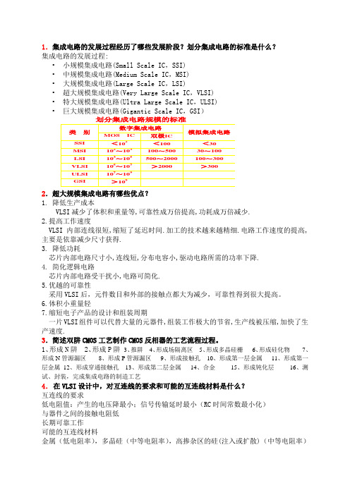
1.集成电路的发展过程经历了哪些发展阶段?划分集成电路的标准是什么?集成电路的发展过程:•小规模集成电路(Small Scale IC,SSI)•中规模集成电路(Medium Scale IC,MSI)•大规模集成电路(Large Scale IC,LSI)•超大规模集成电路(Very Large Scale IC,VLSI)•特大规模集成电路(Ultra Large Scale IC,ULSI)•巨大规模集成电路(Gigantic Scale IC,GSI)划分集成电路规模的标准2.超大规模集成电路有哪些优点?1. 降低生产成本VLSI减少了体积和重量等,可靠性成万倍提高,功耗成万倍减少.2.提高工作速度VLSI内部连线很短,缩短了延迟时间.加工的技术越来越精细.电路工作速度的提高,主要是依靠减少尺寸获得.3. 降低功耗芯片内部电路尺寸小,连线短,分布电容小,驱动电路所需的功率下降.4. 简化逻辑电路芯片内部电路受干扰小,电路可简化.5.优越的可靠性采用VLSI后,元件数目和外部的接触点都大为减少,可靠性得到很大提高。
6.体积小重量轻7.缩短电子产品的设计和组装周期一片VLSI组件可以代替大量的元器件,组装工作极大的节省,生产线被压缩,加快了生产速度.3.简述双阱CMOS工艺制作CMOS反相器的工艺流程过程。
1、形成N阱2、形成P阱3、推阱4、形成场隔离区5、形成多晶硅栅6、形成硅化物7、形成N管源漏区8、形成P管源漏区9、形成接触孔10、形成第一层金属11、形成第一层金属12、形成穿通接触孔13、形成第二层金属14、合金15、形成钝化层16、测试、封装,完成集成电路的制造工艺4.在VLSI设计中,对互连线的要求和可能的互连线材料是什么?互连线的要求低电阻值:产生的电压降最小;信号传输延时最小(RC时间常数最小化)与器件之间的接触电阻低长期可靠工作可能的互连线材料金属(低电阻率),多晶硅(中等电阻率),高掺杂区的硅(注入或扩散)(中等电阻率)5.在进行版图设计时为什么要制定版图设计规则?—片集成电路上有成千上万个晶体管和电阻等元件以及大量的连线。
超大规模集成电路设计 作业 问题解答

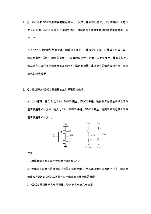
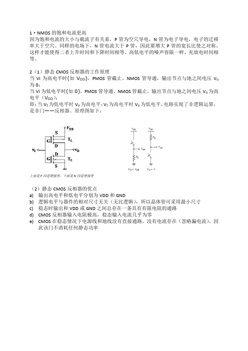
1. Q :PMOS 和NMOS 晶体管有相同的W ,L 尺寸,并且他们的V gs ,V ds 也相同,该电压使PMOS 和NMOS 同时处于饱和工作区,请问这两个晶体管中谁的饱和电流更高,为什么?A :NMOS 的饱和电流更高,和载流子有关,P 管是空穴导电,N 管电子导电,电子的迁移率大于空穴,同样的电场下,N 管的电流大于P 管,因此要增大P 管的宽长比,使之对称,这样才能使得两者上升时间下降时间相等、高低电平的噪声容限一样、充电放电的时间相等2. Q :论述静态CMOS 反相器的工作原理及其优点。
A :工作原理:输入In 为1时,PMOS 截止,NMOS 导通,输出节点和接地节点之间存在直接通路Out 为0,输入为0时,PMOS 导通,NMOS 截止,输出节点和电源之间存在直接通路Out 为1。
V DD优点:1)输出高电平和低电平分别为VDD 和GND ;2)逻辑电平与器件的相对尺寸无关(无比逻辑),所以晶体管可采用最小尺寸,稳态时输出和VDD 或GND 之间总存在一条具有有限电阻的通路; 3)CMOS 反相器输入电阻极高,稳态输入电流几乎为零;4)CMOS 在稳态情况下电源线和地线没有直接通路,没有电流存在(忽略漏电流),因此该门不消耗任何静态功耗。
3. Q :两个串联的NMOS 晶体管M1,M2(如下图),已知M1和M2的体电压,M1的源、漏电压,电流,及M1和M2的尺寸(W/L ),求M2的阈值电压,漏电压,并指出M2当前处于哪一工作区(注:NMOS 晶体管零阈值电压V T0n =0.6 V ,费米电势近似 -0.3V ,体效应系数为0.4,工艺跨导为8.9x10⁻⁵A/V 2,V DSATn =0.63V 忽略沟道调制影响)。
A :222202SB S B V V V V =−=−=,0T T V V γ=+,20.60.40.94T V V =+=,2222DS GS GS T V V V V =>−,所以M2可能处于夹断饱和工作区,还有可能发生速度饱和,因此先考虑发生夹断饱和时的漏电压,()2222n D GS T k I V V =−,222GS T T V V V ==20.94 2.16GS V V ==,221 2.162 4.16D GS D V V V V =+=+=,由2D DSATn V V >,确定M2发生速度饱和,因此222()2DSAT D n GS T DSAT V I k V V V ⎛⎞=−−⎜⎟⎝⎠,2222DSAT D n GS T DSATV I k V V V ⎛⎞+⎜⎟⎝⎠=+,32520.2100.6338.91020.94 2.440.63GS V V −−×⎛⎞+⎜⎟××⎝⎠=+=, 2212.442 4.44D GS D V V V V =+=+=4. Q :有三个反相器组成的反相器链,输入电容为C i =1pF ,负载电容为C L =1000pF ,如果第一个反相器I 1的尺寸为1,传播延时t p1为70ps (注:γ=1),(1) 请确定其他两个反相器I 2、I 3的尺寸,使反相器链的传播延时最小,并计算该情况下的最小延时;(2) 如果第一个反相器I 1尺寸不变,并且允许在其后边增加任意数目的反相器使反相器链的延时最小,请确定插入反相器的数目,并计算该情况下的最小延时。
硅超大规模集成电路工艺技术—理论、实践与模型_课后习题答案
1.2. Assuming dopant atoms are uniformly distributed in a silicon crystal, how far apart arethese atoms when the doping concentration is a). 1015 cm -3, b). 1018 cm -3, c). 5x1020 cm -3.N Answer:The average distance between the dopant atoms would just be one over the cube root of the dopant concentration:x =N A -1/3a)x =1x1015cm-3()-1/3=1x10-5cm =0.1μm =100nm b)x =1x1018cm-3()-1/3=1x10-6cm =0.01μm =10nmc)x =5x1020cm-3()-1/3=1.3x10-7cm =0.0013μm =1.3nm1.3. Consider a piece of pure silicon 100 µm long with a cross-sectional area of 1 µm2. Howmuch current would flo w through this “resistor” at room temperature in response to an applied voltage of 1 volt?Answer: If the silicon is pure, then the carrier concentration will be simply n i . At room temperature, n i≈ 1.45 x 1010 cm -3. Under an applied field, the current will be due to drift and hence,I =I n +I p =qAn i μn +μp ()ε=1.6x10⁻¹⁹coul ()10-8cm2()1.45x10¹⁰carrierscm-3()2000cm 2volt-1sec-1()1volt 10-2cm ⎛ ⎝ ⎫⎭=4.64x10⁻¹²amps or 4.64pA1.10. A state-of-the-art NMOS transistor might have a drain junction area of 0.5 x 0.5 µm.Calculate the junction capacitance associated with this junction at an applied reverse bias of 2 volts. Assume the drain region is very heavily doped and the substrate doping is 1 x 1016 cm -3. Answer:The capacitance of the junction is given by Eqn. 1.25.C A =εS x d =q εS 2N A ND N A +N D ⎛ ⎝ ⎫ ⎭ ⎪ 1φi ±V ()⎡ ⎣ ⎢⎤ ⎦ ⎥The junction built-in voltage is given by Eqn. 1.24. N D is not specified except that it is very large, so we take it to be 1020 cm -3 (roughly solid solubility). The exact choice for N D doesn't make much difference in the answer.φi =kT q ln N D N An i 2⎛ ⎝ ⎫ ⎭⎪ =.0259volts ()ln 1020cm -3()1016cm -3()1.45x1010cm-3()2⎛ ⎝ ⎫⎭⎪ ⎪ =0.934 voltsSince N D >> N A in this structure, the capacitance expression simplifies toC A ≅εSW=qεS2N A()1φi±V()⎡⎣⎢⎤⎦⎥=1.6x10⁻¹⁹coul()11.7()1016cm-3()8.86x10⁻¹⁴Fcm-1()2()2.934volts()⎡⎣⎢⎤⎦⎥ =1.68x10⁻⁸Fcm-2Given the area of the junction (0.25 x 10⁻⁸ cm2, the junction capacitance is thus 4.2 x 10⁻¹⁷ Farads.3.2. A boron-doped crystal pulled by the Czochralski technique is required to have aresistivity of 10 Ω cm when half the crystal is grown. Assuming that a 100 gm pure silicon charge is used, how much 0.01 Ω cm boron doped silicon must be added to the melt? For this crystal, plot resistivity as a function of the fraction of the melt solidified. Assume k 0 = 0.8 and the hole mobility µp = 550 cm 2 volt -1 sec -1.Answer:Using the mobility value given, and ρ=1q μN A we have:10 Ω cm ⇒ N A = 1.14 x 1015 cm -3 and 0.01 Ω cm ⇒ N A = 1.14 x 1018 cm -3From Eqn. 3.38, C S =C O k O 1-f ()k O -1and we want C S = 1.14 x 1015 cm -3 when f =0.5. Thus, solving for C 0 the initial doping concentration in the melt, we have:C 0=1.14x10150.81-0.5()0.2=1.24x1015cm -3But C 0=I 0V 0=# of impurities unit vol of me lt =(Doping)(Vol. of 0.01 Ωcm)Vol 100 gm Si∴ Wgt added of 0.01 Ω c m Si = C 0Doping ⎛ ⎝ ⎫⎭ 100gm ()=0.109gmThe resistivity as a function of distance is plotted below and is given byρx ()=1q μN A x ()=1-f ()1-k 0q μC 0k 0=11.5Ωcm 1-f ()0.2R e s i s t i v i t y0.20.40.60.81Fraction S olidified - f3.3. A Czochralski crystal is pulled from a melt containing 1015 cm -3 boron and 2x1014 cm -3phosphorus. Initially the crystal will be P type but as it is pulled, more and more phosphorus will build up in the liquid because of segregation. At some point the crystal will become N type. Assuming k O = 0.32 for phosphorus and 0.8 for boron, calculate the distance along the pulled crystal at which the transition from P to N type takes place.Answer:We can calculate the point at which the crystal becomes N type from Eqn. 3.38 as follows:C S Phos ()=C 0k 01-f ()k 0-1=2x10¹⁴()0.32()1-f ()-0.68C S Boron ()=C 0k 01-f ()k 0-1=1015()0.8()1-f ()-0.2At the point where the cross-over occurs to N type, these two concentrations will be equal. Solving for f, we findf ≅0.995Thus only the last 0.5% of the crystal is N type.3.6. Suppose your company was in the business of producing silicon wafers for thesemiconductor industry by the CZ growth process. Suppose you had to produce the maximum number of wafers per boule that met a fairly tight resistivity specification. a). Would you prefer to grow N type or P type crystals? Why?b). What dopant would you use in growing N-type crystals? What dopant would you use in growing P type crystals? ExplainAnswer:a). Boron has the segregation coefficient closest to unity of all the dopants. Thus it produces the most uniform doping along the length of a CZ crystal. Thus P type would be the natural choice.b). For P type, the obvious (and only real choice) is boron as explained in part a). For N type crystals Fig. 3-18 shows that either P or As would be a reasonable choice since their segregation coefficients are quite close and are better than Sb. Table 3-2 indicates that P might be slightly preferred over As because its k O value is slightly closer to 1.4.1. An IC manufacturing plant produces 1000 wafers per week. Assume that each wafer contains 100 die, each of which can be sold for $50 if it works. The yield on these chips is currently running at 50%. If the yield can be increased, the incremental income is almost pure profit because all 100 chips on each wafer are manufactured whether they work or not. How much would the yield have to be increased to produce an annual profit increase of $10,000,000?Answer:At 1000 wafers per week, the plant produces 52,000 wafers per year. If each wafer has 50 good die each of which sells for $50, the plant gross income is simplyIncome = (52,000)(50)($50) = $130,000,000 per year.To increase this income by $10,000,000 requires that the yield increase by10130≅7.7%4.3. As MOS devices are scaled to smaller dimensions, gate oxides must bereduced in thickness.a. As the gate oxide thickness decreases, do MOS devices become more or lesssensitive to sodium contamination? Explain.b. As the gate oxide thickness decreases, what must be done to the substrate doping (oralternatively the channel V TH implant, to maintain the same V TH? Explain.Answer:a). From the text, Na+ contamination causes threshold voltage instabilities in MOS devices.Also from Eqn. 4.1, the threshold voltage is given byV TH=V FB+2φf+2εS qN A2φf()C OX+qQ MC OXAs the gate oxide thickness decreases, C OX increases, so the same amount of mobile charge Q M will have less effect on V TH as oxides get thinner. Therefore MOS devices are less sensitive to sodium contamination.b). Using the same expression for V TH as in part a), we observe that as the oxide thickness decreases, (C OX increases), to maintain the same V TH, N A will have to increase. N A willactually have to increase by the square root of the oxide thickness decrease to keep V TH constant.4.4. A new cleaning procedure has been proposed which is based on H2O saturated with O2as an oxidant. This has been suggested as a replacement for the H2O2 oxidizing solution used in the RCA clean. Suppose a Si wafer, contaminated with trace amounts of Au, Fe and Cu is cleaned in the new H2O/O2solution. Will this clean the wafer effectively?Why or why not? Explain.Answer:As described in the text, cleaning metal ions off of silicon wafers involves the following chemistry:M↔M z++ze-The cleaning solution must be chosen so that the reaction is driven to the right because this puts the metal ions in solution where they can be rinsed off. Since driving the reaction to the right corresponds to oxidation, we need an oxidizing solution to clean the wafer.H2O/O2 is certainly an oxidizing solution. But whether it cleans effectively or not depends on the standard oxidation potential of the various possible reactions. From Table 4-3 in the text, we have:The stronger reactions (dominating) are at the bottom.Thus the H2O/O2 reaction will clean Fe and Cu, but it will not clean Au off the wafer.4.5. Explain why it is important that the generation lifetime measurement illustrated inFigure 4-19 is done in the dark.Answer:The measurement depends on measuring carriers generated thermally in the silicon substrate (or at the surface). If light is shining on the sample, then absorbed photons can also generate the required carriers. As a result, the extracted generation lifetime with the light on would really be measuring the intensity of the incident light and not a basic property of the silicon material.5.1. Calculate and plot versus exposure wavelength the theoretical resolution and depth offocus for a projection exposure system with a NA of 0.6 (about the best that can be done today). Assume k 1 = 0.6 and k 2 = 0.5 (both typical values). Consider wavelengths between 100 nm and 1000 nm (DUV and visible light). ). Indicate the common exposure wavelengths being used or considered today on your plot (g-line, i-line, KrF and ArF). Will an ArF source be adequate for the 0.13 µm and 0.1 µm technology generations according to these simple calculations?Answer:The relevant equations are simply∴R =k 1 λNA =0.6λ0.6 a nd DOF =±k 2λNA ()2=±0.5λ0.6()2These equations are plotted below. Note that the ArF (193 nm) will not reach 0.13 µm or 0.1 µm resolution according to these simple calculations. In fact, with more sophisticated techniques such as phase shift masks, off axis illumination etc., ArF is expected to reach 0.13 µm and perhaps the 0.1 µm generations.R e s o l u t i o n , D O F 祄20040060080010001200Exposure Wavelength nm5.3. An X-ray exposure system uses photons with an energy of 1 keV. If the separation between the mask and wafer is 20 µm, estimate the diffraction limited resolution that is achievable by this system.Answer:The equivalent wavelength of 1 keV x-rays is given byE =h ν=hc λ∴ λ=hc E=4.14x10⁻¹⁵eVsec ()3x1010cm sec -1()103eV=1.24x10⁻⁷cm =1.24 nmX-ray systems operate in the proximity printing mode, so that the theoretical resolution is given by Eqn. 5.12:Resolution =λg =1.24x10⁻³μm ()20μm ()=0.15μm5.8. As described in this chapter, there are no clear choices for lithography systems beyondoptical projection tools based on 193-nm ArF eximer lasers. One possibility is an optical projection system using a 157-nm F 2 excimer laser.a. Assuming a numerical aperture of 0.8 and k 1 = 0.75, what is the expected resolution of such a system using a first order estimate of resolution?b. Actual projections for such systems suggest that they might be capable of resolving features suitable for the 2009 0.07 µm generation. Suggest three approaches to actually achieving this resolution with these systems.Answera). The simple formula for resolution isR =k 1λNA =0.750.157μm0.8=0.147μmb). The calculated resolution in part a is a factor of two larger than required for the 0.07 µm generation. Therefore some “tricks” will have to be used to actually achieve such resolution. There are a number of possibilities:1. Use of phase-shift masks. This technique, discussed in this chapter, has the potential for significant resolution improvements. It works by designing a more sophisticated mask. Simple masks are digital - black or white. Phase shifting adds a second material to the mask features, usually at the edges which shifts the optical phase and sharpens up the aerial image. Sophisticated computer programs are required to design such masks.2. Use of optical proximity correction in the mask design. This is another approach to designing a better mask and as discussed in class, can also improve resolution significantly. The approach involves adding extra features to the mask, usually at corners where features are sharp, to compensate for the high frequency information lost to diffraction effects.3. Off-axis illumination. This allows the optical system to capture some of the higher order diffracted light and hence can improve resolution.5.9. Current optical projection lithography tools produce diffraction limited aerial images. A typical aerial image produced by such a system is shown in the simulation below where a square and rectangular mask regions produce the image shown. (The mask features are the black outlines, the calculated aerial image is the grayscale inside the black rectangles.) The major feature of the aerial image is its rounded corners compared to the sharp square corners of the desired pattern. Explain physically why these features look the way they do, using diffraction theory and the physical properties of modern projection optical lithography tools.Answer:Modern optical projection lithography systems are limited in the resolution they can achieve by diffraction effects. The finite size of the focusing lens means that the high order diffraction components are “lost” and are therefore not available to help in printing a replica of the mask image. But the high frequency spatial components are exactly the components that contain information about “sharp” features, i.e. corners etc. Thus the projected aerial image loses this information and corners become rounded. The only ways to improve the image are by using shorter wavelength light, or a higher NA lens.5.10. Future optical lithography systems will likely use shorter exposure wavelengths toachieve higher resolution and they will also likely use planarization techniques to provide “flat” substrates on which to expose the resist layers. Explain why “flat”substrates will be more important in the future than they have been in the past. Answer:As the wavelength of the exposure system decreases, the depth of focus of the exposure system also decreases. Thus it will be necessary to make sure that the resist in which the image is to be exposed, is flat and does not require much depth of focus. Planarization techniques will be required to accomplish this. This could mean CMP to planarize the substrate before the resist is applied, or it could mean using a spun on resist which planarizes the substrate and which is then covered with a thin, uniform imaging resist layer.6.4. Construct a HF CV plot for a P-type silicon sample, analogous to Fig. 6-9. Explain your plot based on the behavior of holes and electrons in the semiconductor in a similar manner to the discussion in the text for Fig. 6.9. Answer:C ODV GGQ GQ IQ DThe C-V plot looks basically the same as the N substrate example in the text, that we discussed in class, except that the horizontal axis is flipped. For negative applied gate voltages, the majority carrier holes in the substrate are attracted to the surface. This is the accumulation region a) above. We measure just C OX for the capacitance since there is no depletion in the substrate. For + V G, the holes are driven away from the surface creating first a depletion region as in b) and finally an inversion layer of electrons as in c). Themeasured capacitance drops as we move into depletion and finally reaches a minimum value after an inversion layer forms.The C-V curves shown are high frequency curves. As discussed in the text, the capacitance remains at its minimum value for + V G values greater than V TH because the inversion layer electrons cannot be created or destroyed as fast as the signal is changing. Hence the small AC signal must “wiggle” the bottom of the depletion region to balance ∆V G.6.6. In a small MOS device, there may be a statistical variation in V T due to differences inQ F from one device to another. In a 0.13 µm technology minimum device (gate oxide area = 0.1µm x 0.1µm) with a 2.5nm gate oxide, what would the difference in threshold voltage be for devices with 0 or 1 fixed charge in the gate oxide?Answer:The oxide capacitance isC ox=εAd=3.9⨯8.854⨯10-14()0.1⨯10-4()0.1⨯10-4()2.5⨯10-7=1.38⨯10-16The change in threshold voltage is given by∆V T=qQ FC ox=1.6⨯10-19()1()1.38⨯10-16=1.1mVThis shows that a single electron trap in a gate oxide will have a negligible effect on thethreshold voltage at this technology generation.6.12 A silicon wafer is covered by an SiO2 film 0.3 μm thick.Edeo9 a. What is the time required to increase the thickness by 0.5 μm by oxidation in H2O at 1200˚C?b. Repeat for oxidation in dry O2at 1200˚C.Answer:We will perform the calculation for <111> silicon wafers. For <100> wafers, the linear rate constant should be divided by 1.68.a. At 1200˚C, in H2OB=3.86⨯102exp-0.78 kT⎛ ⎝ ⎫⎭ =0.829μm2/hrB A =1.63⨯108exp-2.05kT⎛⎝⎫⎭ =15.86μm/hrA=0.052μmThe initial oxide, if grown at 1200˚C would have taken this long to growτ=x i2+Ax iB=0.3()2+0.052()0.3()0.829=0.127hrThe time required to grow 0.8μm at 1200˚C isτ=x i 2+Ax i B =0.8()2+0.052()0.8()0.829=0.822hrThus, the time required to add 0.5μm to an existing 0.3μm film is0.822-0.127=0.695hr or 41.7 minutes.b. At 1200˚C, in dry oxygenB =7.72⨯102exp - 1.23k(1200+273)⎛ ⎝ ⎫⎭ =0.048μm 2/hrB A =6.23⨯106exp -2.0kT ⎛ ⎝ ⎫⎭ =0.899μm /hrA =0.053μmThe initial oxide would have taken 2.206 hours to grow in dry oxygen, it would require 14.217 hours to grow 0.8μm , thus would require an additional 12 hours to add 0.5μm to an existing 0.3μm film.6.13. Suppose an oxidation process is used in which (100) wafers are oxidized in O 2 for threehrs. at 1100˚C, followed by two hrs. in H 2O at 900˚C, followed by two hrs in O 2 at 1200˚C. Use Figs. 6-19 and 6-20 in the text to estimate the resulting final oxide thickness. Explain how you use these figures to calculate the results of a multi-step oxidation like this.Answer:We can use these figures to estimate the oxide thickness as follows. First, we use Fig. 6-19 for the first dry oxidation cycleA three hour oxidation at 1100˚C produces an oxide thickness of about 0.21 µm. We nextuse Fig. 6-20 for the wet oxidation as shown below. The oxidation is 2 hrs in H 2O at 90 ˚C. We start by finding the point on the 900˚C curve that corresponds to 0.21 µm since this is the starting oxide thickness. This is point A. We then move along the 900˚C curve by two hours to point B. This corresponds to a thickness of about 0.4 µm which is the thickness at the end of the wet oxidation.00.40.81.21.62Ox i d e T h i c k n e s s- m i c r o ns12345678Time - hours9101100 ÞC700 ÞC 1000 ÞC900 ÞC800 ÞCABWe now go back to Fig. 6-19 for the final dry O 2 cycle. This process is 2 hrs at 1200˚C. Westart by finding the point on the 1200˚C curve that corresponds to a starting oxide thickness of 0.4 µm. T his is point A below. We then increment the time by 2 hrs along the 1200˚C curve, to arrive at a final oxide thickness of about 0.5 µm.6.18. Silicon on Insulator or SOI is a new substrate material that is being considered forfuture integrated circuits. The structure, shown below, consists of a thin single crystal silicon layer on an insulating (SiO 2) substrate. The silicon below the SiO 2 provides mechanical support for the structure. One of the reasons this type of material is being considered, is because junctions can be diffused completely through the thin silicon layer to the underlying SiO 2. This reduces junction capacitances and produces faster circuits. Isolation is also easy to achieve in this material, because the thin Si layer can be completely oxidized, resulting in devices completely surrounded by SiO 2. A LOCOS process is used to locally oxidize through the silicon as shown on the right below. Assuming the LOCOS oxidation is done in H 2O at 1000˚C, how long will it take to oxidize through the 0.3 µm silicon layer? Calculate a numerical answer using the Deal Grove model.Answer:To oxidize completely through a 0.3 µm silicon layer, we will need to grow (2.2)(0.3 µm) = 0.66 µm of SiO 2. At 1000˚C in H 2O, the Deal Grove rate constants are given by (Table 6-2):B =3.86x10²exp -0.78eV kT ⎛ ⎝ ⎫⎭ =0.316μm 2hr -1B A =1.63x1081.68exp -2.05eV kT ⎛ ⎝ ⎫ ⎭ =0.747μmhr -1∴t =0.66()20.316+0.660.747≅2.25 hours6.23. As part of an IC process flow, a CVD SiO 2 layer 1.0 µm thick is deposited on a <100>silicon substrate. This structure is then oxidized at 900˚C for 60 minutes in an H 2O ambient. What is the final SiO 2 thickness after this oxidation? Calculate an answer, do not use the oxidation charts in the text .Answer:At 900˚C in H 2O, the oxidation rate constants are given by:B =3.86x10²exp -0.788.62x10-5()1173()⎛ ⎝ ⎫ ⎭ ⎪ μm 2 hr -1=0.17 μm 2 hr -1B A =1.63x1081.68exp - 2.058.62x10-5()1173()⎛ ⎝ ⎫⎭ ⎪ μm hr -1=0.152 μm hr -1The initial oxide on the wafer is 1.0 µm thick. This corresponds to a τ ofτ=1()2+1()0.170.152⎛ ⎝⎫ ⎭0.17=12.46 hoursThus the final oxide thickness is given byx o =0.172()0.152()1+13.461.11()24()0.17()-1⎧ ⎨ ⎪ ⎩ ⎪ ⎫⎬ ⎪ ⎭ ⎪=1.064 μmThus not much additional oxide grows.Chapter 7 Problems7.1. A resistor for an analog integrated circuit is made using a layer of deposited polysilicon0.5 µm thick, as shown below.Polysilicon (a) (a)The doping the polysilicon is 1⨯1016 cm -3. The carrier mobilityμ=100cm 2V -1se c -1 is low because of scattering at grain boundaries. If theresistor has L=100µm, W=10µm, what is its resistance in Ohms?(b) (b) A thermal oxidation is performed on the polysilicon for 2 hours at 900˚C inH 2O . Assuming B/A for polysilicon is 2/3 that of <111> silicon, what is thepolysilicon thickness that remains.(c) (c) Assuming that all of the dopant remains in the polysilicon (i.e. does notsegregate to oxide), what is the new value of the resistor in (a). Assume the mobility does not change.Answer:(a)ρ=1nq μ=11⨯1016()1.6⨯10-19()100()=6.25ΩcmρS =ρx j = 6.250.5⨯10-4=125k ΩR =10010ρS =1.25M Ω(10square s )(b) The linear rate coefficient at 900˚C isB A ⎛ ⎝ ⎫ ⎭ poly =231.63⨯108exp -2.05kT ⎛ ⎝ ⎫ ⎭ ⎛ ⎝ ⎫ ⎭=0.170μm hr -1The parabolic rate constant for poly is unchanged:B poly =3.86⨯102exp -0.78kT ⎛ ⎝ ⎫⎭ =0.172μm 2hr -1A poly =1.01μmThe oxide thickness isx o =A 21+tA 2/4B -1⎧ ⎨ ⎩ ⎫ ⎬ ⎭x o =1.0121+21.01()2/40.172()-1⎧ ⎨ ⎩ ⎫ ⎬ ⎭ =0.27μmThis oxide consumes a silicon thickness of 0.45*0.27=0.12 µm, leaving a remaining polysilicon thickness of 0.5-0.12=0.38 µm and contains all the dopant with a concentration of1⨯1016()0.50.38=1.31⨯1016cm-3(c) Since the concentration has gone up and the thickness has gone down by the same factor, the polysilicon restivity and hence the resistance of the line remains the same.7.4. Suppose we perform a solid solubility limited predeposition from a doped glass sourcewhich introduces a total of Q impurities / cm 2.(a) (a) If this predeposition was performed for a total of t minutes, how long would ittake (total time) to predeposit a total of 3Q impurities / cm 2 into a wafer if the predeposition temperature remained constant.(b) (b) Derive a simple expression for theDt ()drive -in which would be required to drive the initial predeposition of Q impurities / cm 2 sufficiently deep so that the final surface concentration is equal to 1% of the solid solubility concentration. Thiscan be expressed in terms ofDt ()predepand the solid solubility concentrationC S .Answer:(a)Q =2C SπDt ⇒Q ∝t∴3Q ⇒9t(b)C 0,t ()drive -in =QπDt =0.01C SQ =2C SπDt ()predep∴2πDt ()predep Dt ()drive -in =0.01∴Dt ()drive -in =200π⎛ ⎝ ⎫ ⎭ 2Dt ()predep7.7. A boron diffusion is performed in silicon such that the maximum boron concentration is1 x 1018 cm -3. For what range of diffusion temperatures will electric field effects and concentration dependent diffusion coefficients be important?Answer:Electric field effects and concentration dependent diffusion are both important when the doping concentration exceeds the intrinsic electron (or hole) concentration. The intrinsic orbackground electron concentration is n i which increases with higher temperature. This provides a background sea of electrons or holes in the lattice at a given temperature. If the doping exceeds this concentration, then these extrinsic effects are important.When the temperature is below the temperature where n i =1⨯1018/cm 3, these effectswill become dominant since they often depend on n /n i (where n =N A or n =N D to a first approximation).n i =3.9⨯1016T 32exp -0.605kT ⎛ ⎝ ⎫⎭By trial and error, n i =1⨯1018/cm 3at T=720C.Therefore, extrinsic effects become important below 720˚C.7.15. A silicon wafer is uniformly doped with boron (2 x 1015 cm -3) and phosphorus (1 x 1015cm -3) so that it is net P type. This wafer is then thermally oxidized to grow about 1 µm of SiO 2. The oxide is then stripped and a measurement is made to determine the doping type of the wafer surface. Surprisingly it is found to be N type. Explain why the surface was converted from P to N type. Hint: Consider the segregation behavior of dopants when silicon is oxidized.Answer:The boron segregates preferentially into the growing oxide, thus depleting the surface concentration in the silicon. The phosphorus on the other hand preferentially segregates (piles-up) on the silicon side of the interface. Both of these effects act in the same direction and tend to make the surface of the silicon more N-type.It is for this reason that a P-type “channel stop” implant is almost always needed under a locally oxidized lightly doped P-type region, to prevent depletion of the P-type dopant in the substrate and in the worst case to prevent an N-type channel from forming. 7.20. Fig. 7.38 shows that a wet oxidation produces a significantly higher C I /C I *than doesa dry O 2 oxidation. Explain quantitatively why this should be the case. Answer:BecauseC I ∝dx dta faster oxidation rate produces a higher interstitial supersaturation. Thus, wet oxidationproduces a higher C I/C I * than dry oxidation, for the same time at the same temperature. Chapter 8 Problems8.1. Arsenic is implanted into a lightly doped p-type Si substrate at an energy of 75keV . Thedose is 1⨯1014/cm 2. The Si substrate is tilted 7˚ with resp ect to the ion beam to make it appear amorphous. The implanted region is assumed to be rapidly annealed so that complete electrical activation is achieved. What is the peak electron concentration produced?Answer:From Fig. 8-3, the range and standard deviation for 75 keV arsenic areR P =0.05μm ∆R P =0.02μmThe peak concentration isC P =Q 2π∆R P =1⨯10142π0.02⨯10-4()=2⨯1019cm -3Assuming all the dose is active, then the peak electron concentration is equal to the peak dopant concentration.8.4. How thick does a mask have to be to reduce the peak doping of an implantby a factor of 10,000 at the mask/substrate boundary. Provide an equation in terms of the Range and the Standard Deviation of the implant profile.Answer:We want to reduce the peak doping N P * in the mask at range R P * by 10,000 at themask/substrate boundary. We will use the equation which describes the profile of an implantin a mask layerN *(d)=N P *exp -d -R P *()22∆R P *2⎡ ⎣ ⎢ ⎢ ⎤ ⎦⎥ ⎥WhenN *(d)N P*=10-4we haved =R P *+4.3∆R P *8.6. The equations below provide a reasonable analytical description for some of thediffusion processes indicated schematically in the diagrams on the following page. Put the equation number (a-f) on each figure that is the best match. Equations may be。
超大规模集成电路答案
⎞ ⎟⎠
(1
+
λnVM
)
= 115×10−6 × 2× 0.63× (1.05 − 0.4 − 0.63 / 2)(1+ 0.06×1.05)
= 52 ×10−6 A
g = − k Vn DSATn + k Vp DSATp
ID
(VM
)(λn
−
λ p
)
= − 1 2 ×115×10−6 × 0.63 + 3× 30×10−6 ×1
A:Al1 导线平面电容:(0.1×103μm2) ×30aF/μm2=3pF Al1 导线边缘电容:2×(0.1×106μm) ×40aF/μm=8pF Al1 导线总电容:CW=11pF Al1 导线电阻:RW=0.075Ω/□×(0.1×106μm)/ (1μm)=7.5kΩ Al1 导线的 r 和 c 值:c=110aF/μm;r=0.075Ω/μm
由VD2 > VDSATn ,确定 M2 发生速度饱和,因此
ID
=
kn
⎛ ⎜⎝ (VGS 2
− VT 2 )VDSAT
2
− VDSAT 2
⎞ ⎟⎠
,
VGS 2
= VT 2
+
⎛ ⎜ ⎝
ID kn
2
+ VDSAT 2
VDSAT
⎞ ⎟ ⎠
,
VGS 2
=
0.94
+
⎛ ⎜⎝
பைடு நூலகம்
0.2 ×10⁻³ 3× 8.9 ×10−5
( ) ID
=
kn 2
VGS 2 − VT 2
2 , VGS 2 = VT 2 +
2ID kn
(完整版)集成电路设计复习题及解答

集成电路设计复习题绪论1.画出集成电路设计与制造的主要流程框架。
2.集成电路分类情况如何?集成电路设计1.层次化、结构化设计概念,集成电路设计域和设计层次2.什么是集成电路设计?集成电路设计流程。
(三个设计步骤:系统功能设计逻辑和电路设计版图设计)3.模拟电路和数字电路设计各自的特点和流程4.版图验证和检查包括哪些内容?如何实现?5.版图设计规则的概念,主要内容以及表示方法。
为什么需要指定版图设计规则?6.集成电路设计方法分类?(全定制、半定制、PLD)7.标准单元/门阵列的概念,优点/缺点,设计流程8.PLD设计方法的特点,FPGA/CPLD的概念9.试述门阵列和标准单元设计方法的概念和它们之间的异同点。
10.标准单元库中的单元的主要描述形式有哪些?分别在IC设计的什么阶段应用?11.集成电路的可测性设计是指什么?Soc设计复习题1.什么是SoC?2.SoC设计的发展趋势及面临的挑战?3.SoC设计的特点?4.SoC设计与传统的ASIC设计最大的不同是什么?5.什么是软硬件协同设计?6.常用的可测性设计方法有哪些?7. IP的基本概念和IP分类8.什么是可综合RTL代码?9.么是同步电路,什么是异步电路,各有什么特点?10.逻辑综合的概念。
11.什么是触发器的建立时间(Setup Time),试画图进行说明。
12.什么是触发器的保持时间(Hold Time),试画图进行说明。
13. 什么是验证,什么是测试,两者有何区别?14.试画图简要说明扫描测试原理。
绪论1、 画出集成电路设计与制造的主要流程框架。
2、集成电路分类情况如何?集成电路设计1. 层次化、结构化设计概念,集成电路设计域和设计层次分层分级设计和模块化设计.将一个复杂的集成电路系统的设计问题分解为复杂性较低的设计级别,⎪⎪⎪⎪⎪⎪⎪⎪⎪⎪⎪⎪⎪⎪⎪⎪⎪⎩⎪⎪⎪⎪⎪⎪⎪⎪⎪⎪⎪⎪⎪⎪⎪⎪⎪⎨⎧⎪⎪⎪⎪⎩⎪⎪⎪⎪⎨⎧⎩⎨⎧⎩⎨⎧⎪⎪⎪⎪⎩⎪⎪⎪⎪⎨⎧⎪⎪⎪⎪⎪⎪⎩⎪⎪⎪⎪⎪⎪⎨⎧⎩⎨⎧⎪⎪⎪⎪⎩⎪⎪⎪⎪⎨⎧⎩⎨⎧⎪⎩⎪⎨⎧按应用领域分类数字模拟混合电路非线性电路线性电路模拟电路时序逻辑电路组合逻辑电路数字电路按功能分类GSI ULSI VLSI LSI MSI SSI 按规模分类薄膜混合集成电路厚膜混合集成电路混合集成电路B iCMOS B iMOS 型B iMOS CMOS NMOS PMOS 型MOS双极型单片集成电路按结构分类集成电路这个级别可以再分解到复杂性更低的设计级别;这样的分解一直继续到使最终的设计级别的复杂性足够低,也就是说,能相当容易地由这一级设计出的单元逐级组织起复杂的系统。
大规模集成电路习题与答案
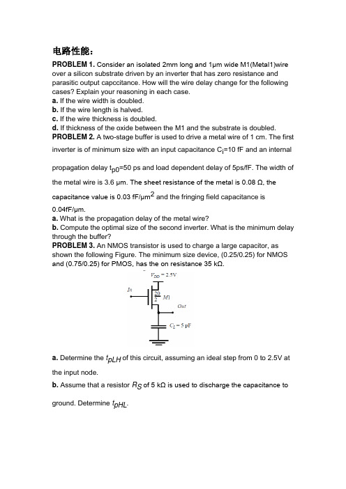
电路性能:PROBLEM 1. Consider an isolated 2mm long and 1μm wide M1(Metal1)wire over a silicon substrate driven by an inverter that has zero resistance and parasitic output capccitance. How will the wire delay change for the following cases? Explain your reasoning in each case.a. If the wire width is doubled.b. If the wire length is halved.c. If the wire thickness is doubled.d. If thickness of the oxide between the M1 and the substrate is doubled. PROBLEM 2. A two-stage buffer is used to drive a metal wire of 1 cm. The first inverter is of minimum size with an input capacitance C i=10 fF and an internalpropagation delay t p0=50 ps and load dependent delay of 5ps/fF. The width of the metal wire is 3.6 μm. The sheet resistance of the metal is 0.08 Ω, the capacitance value is 0.03 fF/μm2 and the fringing field capacitance is0.04fF/μm.a. What is the propagation delay of the metal wire?b. Compute the optimal size of the second inverter. What is the minimum delay through the buffer?PROBLEM 3. An NMOS transistor is used to charge a large capacitor, as shown the following Figure. The minimum size device, (0.25/0.25) for NMOS and (0.75/0.25) for PMOS, has the on resistance 35 kΩ.a. Determine the t pLH of this circuit, assuming an ideal step from 0 to 2.5V at the input node.b. Assume that a resistor R S of 5 kΩ is used to discharge the capacitance toground. Determine t pHL.c. The NMOS transistor is replaced by a PMOS device, sized so that k p is equal to the k n of the original NMOS. Will the resulting structure be faster? Explain why or why not.PROBLEM 4.The figure below assembles a RTL circuit where the active device is a NMOS transistor which has a resistive load. Assume the switch model behavior of the NMOS transistor. When V in <1.25V, the resistance of the transistor is infinite. When V in ≥1.25V, the transistor can be modeled as having a resistance of 150 ohms.A. Determine the values for V OH and V OL . Explain your answer.B. Calculate t pLH and t pHL to obtain the average propagation delay, t p .Solution:Vin 50fFPROBLEM 5. The next figure shows two implementations of MOS inverters. The first inverter uses only NMOS transistors.a. Calculate V OH, V OL, V th for each case.b. Find V IH, V IL, N ML and N MH for each inverter and comment on the results. How can you increase the noise margins and reduce the undefined region? 0.25um CMOS工艺(L=Lmin) MOS管参数Problem 6: We want to design a minimum sized CMOS inverter with 0.25um process( =0.12um). The minimum sized NMOS transistor ’s layers are listed and shown below in Figure below.A. Determine and list the following:a. Minimum Transistor Lengthb. Minimum Transistor Widthc. Minimum Source/Drain Aread. Minimum Source/Drain PerimeterPlease list the design rules you come across that lead to your results.B. We desire the minimum sized CMOS inverter with a symmetrical VTC (V Th =V DD /2) in the 0.25um technology. Calculate the following for the pull-up PMOS transistor in the design.a. Minimum Transistor Lengthb. Minimum Transistor Widthc. Minimum Source/Drain Aread. Minimum Source/Drain PerimeterAssume the following:V DD = 2.5V, and refer to the tables in the below.C. Using the same minimum size inverter from part B, determine the input capacitance (i.e. the load it presents when driven) and the total load capacitance that the inverter presents.D. Calculate t pLH and t pHL to obtain the average propagation delay, t p .Rules are:i) Poly minimum width = 0.24umii) Minimum active width = 0.36umiii) Minimum contact size = 0.24um*0.24umiv) Minimum spacing from contact to gate = 0.24umv) Active enclosure of contact = 0.12umAnswer:A:a. L = 0.24umb. W = 0.48umc. L drain = 0.24um+0.24um+0.12um = 0.6umA D =A S = 0.48 * 0.6um = 0.288 um 2d. P D =P S =0.6um*2+0.48um = 1.68umB:2n T0,Th Th p T0,DD p n R R R p T0,DD n T0,Th V V V V V k k 得出k k 11k 1)V (V V V ⎪⎪⎭⎫ ⎝⎛--+==+⋅++=查表得出一下参数:V T0p = -0.43V V T0n = 0.4V K n ’=115×10-6 A/V 2 K p ’=30×10-6A/V 2 另:L=0.24um, W n =0.48um带入上述公式计算得出:K R =0.965 W p =1.907umWe assume u n =2.5u p and can calculatea. Lp=0.24µmb. W p = 1.907 µmc. A D = 1.907µm *0.6µm =1.1442 µm 2d. P D = 2*0.6µm +1.2µm =3.107 µmC:NMOS:C gn = C ox L n W n = 0.6912 fFNMOS 管衬底接0V ,输出从1→0(V 1=-2.5V 变为V 2=-1.25V):()()()[]()()()[]0.615264fFC C C fF0.2869940.61281.68K C P C 0.44m 0.61V φV φm)(1V V φK fF 32832057022880K C A C 0.5m 0.57V φV φm)(1V V φK dbsw db dbn1eqsw j D dbsw m 11bsw m 12bsw 12m bsw eq eq j D db m 11b m 12b 12m b eq =+==⨯⨯====---⋅----==⨯⨯====---⋅----=----.0侧壁:...底部:输出从0→1(V 1=0V 变为V 2=-1.25V):()()()[]()()()[]fF0.836064C C C fF0.3810240.81281.68K C P C 0.44m 0.81V φV φm)(1V V φK fF 0.455040.7920.288K C A C 0.5m 0.79V φV φm)(1V V φK dbsw db dbn2eqsw j D dbsw m 11bsw m 12bsw 12m bsw eq eq j D db m 11b m 12b 12m b eq =+==⨯⨯====---⋅----==⨯⨯====---⋅----=----.0侧壁:底部:PMOS:C gp = C ox L p W p ) =2.74608 fFPMOS 管衬底接2.5V ,输出从1→0(V 1= 0V 变为V 2=-1.25V):()()()[]()()()[]fF2C C C fF0.58784440.8622K C P C 0.32m 0.86V φV φm)(1V V φK fF 10.7911K C A C 0.48m 0.79V φV φm)(1V V φK dbsw db dbp1eqsw j D dbsw m 11bsw m 12bsw 12m bsw eqsw eq j D db m 11b m 12b 12m b eq 3052886..0109.3侧壁:7174442.9.1442.=+==⨯⨯====---⋅----==⨯⨯====---⋅----=----底部:输出从0→1(V 1=-1.25V 变为V 2= -2.5V):()()()[]()()()[]fF1.7614342C C C fF0.4787860.70.223K C P C 0.32m 0.7V φV φm)(1V V φK fF 10.591.91K C A C 0.48m 0.59V φV φm)(1V V φK dbsw db dbp2eqsw j D dbsw m 11bsw m 12bsw 12m bsw eqsw eq j D db m 11b m 12b 12m b eq =+==⨯⨯====---⋅----==⨯⨯====---⋅----=----109.侧壁:2826482.1442.底部:如果m 以0.5计算:NMOS 管衬底接0V ,输出从1→0(V 1=-2.5V 变为V 2=-1.25V):()()()[]0.596448fFC C C fF0.268120.57281.68K C P C fF 32832057022880K C A C 0.57V φV φm)(1V V φK K dbsw db dbn1eqsw j D dbsw eq j D db m 11b m 12b 12m b eqsw eq =+==⨯⨯===⨯⨯===---⋅----==--.0...底部: 输出从0→1(V 1=0V 变为V 2=-1.25V):()()()[]fF0.826656C C C fF0.3716160.79281.68K C P C fF0.455040.7920.288K C A C 0.79V φV φm)(1V V φK K dbsw db dbn2eqsw j D dbsw eq j D db m 11b m 12b 12m b eqsw eq =+==⨯⨯===⨯⨯===---⋅----==--.0底部:PMOS 管衬底接2.5V ,输出从1→0(V 1= 0V 变为V 2=-1.25V):()()()[]fF 2C C C fF0.54034420.7922K C P C fF1.71744420.79911K C A C 0.79V φV φm)(1V V φK K dbsw db dbp1eqsw j D dbsw eq j D db m 11b m 12b 12m b eqsw eq 2577884..0109.3.1442.=+==⨯⨯===⨯⨯===---⋅----==--底部:输出从0→1(V 1=-1.25V 变为V 2= -2.5V):()()()[]fF 1.6290372C C C fF0.38986860.570.22K C P C fF10.571.91K C A C 0.57V φV φm)(1V V φK K dbsw db dbp2eqsw j D dbsw eq j D db m 11b m 12b 12m b eqsw eq =+==⨯⨯===⨯⨯===---⋅----==--109.32391686.1442.底部:D :C load 计算:C load =C wire +C g +C gd,n +C gd,p +C db,n +C db,p≈C g +C db,n +C db,pC g = C gn + C gp =0.6912+2.74608=3.43728 fF输出从1→0(V 1= 0V 变为V 2=-1.25V):C load≈C g +C db,n +C db,p =6.3578326 fF16.32ps1V )V 4(V ln V V 2V )V (V k C A/V 10230k L W k DD T0n DD T0n DD T0n T0n DD n load PHL 26'n nn n =⎥⎦⎤⎢⎣⎡⎪⎪⎭⎫ ⎝⎛--+--=⨯=⨯=-τ 输出从0→1(V 1=-1.25V 变为V 2= -2.5V):C load≈C g +C db,n +C db,p =6.0347782 fF15.33ps 1V )V 4(V ln V V V 2)V (V k C A/V 10238.375k L W k DD T0p DD T0pDD T0p T0pDD p load PLH 26'p p p p =⎥⎥⎦⎤⎪⎪⎭⎫ ⎝⎛--+⎢⎢⎣⎡--=⨯=⨯=-τ如果以m=0.5,则:输出从1→0(V 1= 0V 变为V 2=-1.25V):C load≈C g +C db,n +C db,p =6.2915162 fF16.147ps1V )V 4(V ln V V 2V )V (V k C DD T0n DD T0n DD T0n T0n DD n load PHL =⎥⎦⎤⎢⎣⎡⎪⎪⎭⎫ ⎝⎛--+--=τ 输出从0→1(V 1=-1.25V 变为V 2= -2.5V):C load≈C g +C db,n +C db,p =5.8929732 fFps 1V )V 4(V ln V V V 2)V (V k C DD T0p DD T0p DD T0p T0pDD p load PLH 97.14=⎥⎥⎦⎤⎪⎪⎭⎫ ⎝⎛--+⎢⎢⎣⎡--=τ PROBLEM 7.We want to design a minimum sized CMOS inverter with 0.25um process(λ=0.12um) and desire the inverter with a symmetrical VTC (V Th =V DD /2) . The minimum sized NMOS transistor’s layers are shown as problem 6. Assume the following:V DD = 2.5V, and refer to the tables in the below.A. Determine the input capacitance (i.e. the load it presents when driven) and the total load capacitance that the inverter presents.B. Calculate t pLH and t pHL to obtain the average propagation delay, t p .PROBLEM 8. Sizing a chain of inverters.a. In order to drive a large capacitance (CL = 20 pF) from a minimum size gate (with input capacitance Ci = 10fF), you decide to introduce a two-staged buffer as shown in the following figure. Assume that the propagation delay of a minimum size inverter is 70 ps. Also assumethat the input capacitance of a gate is proportional to its size. Determine the sizing of the two additional buffer stages that will minimize the propagation delay.b. If you could add any number of stages to achieve the minimum delay, how many stages would you insert?What is the propagation delay in this case?c. Describe the advantages and disadvantages of the methods shown in (a) and (b).PROBLEM 9. Consider a CMOS inverter with the following parameters:V T0,n=1.0V V T0,p=-1.2V μn C ox=45uA/V2μp C ox=25uA/V2 (W/L)n=10 (W/L)p=20The power supply voltage is 5V, and the output load capacitance is 1.5pF.a. Calculate the rise time and the fall time of the output signal using average current method.b. Determine the maximum frequency of a periodic square-wave input signal so that the output voltage can still exhibit a full logic swing from 0V to 5V in each cycle.c. Calculate the dynamic power dissipation at this frequency.d. Assume that the output load capacitance is mainly dominated by fixedfan-out component( which are independent of W n and W p). We want tore-design the inverter so that the propagation delay times are reduced by 25%. Determine the required channel dimensions of the nMOS and the pMOS transistors. How does this re-design influence the switching (inversion) threshold?PROBLEM 10. Consider the following low swing driver consisting of NMOS devi ces M1 and M2. Assume that the inputs IN and IN’ have a 0V to 2.5V swing and that V IN = 0V when V IN’ = 2.5V and vice-versa. Also assume thatthere is no skew between IN and IN’ (i.e., the inverter delay to derive IN from IN is zero).a. What voltage is the bulk terminal of M2 connected to?b. What is the voltage swing on the output node as the inputs swing from 0V to2.5V. Show the low value and the high value.c. Assume that the inputs IN and IN have zero rise and fall times. Assume a zero skew between IN and IN’. Determine the low to high propagation delay for charging the output node measured from the the 50% point of the input to the 50% point of the output. Assume that the total load capacitance is 1pF, including the transistor parasitics.MOS管参数参照题4。
大规模集成电路设计题目及答案
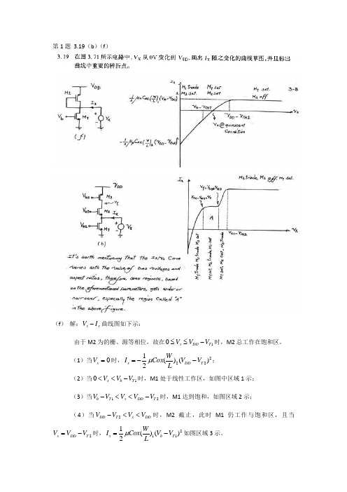
第1题 3.19(b )(f )(f ) 解:x x V I -曲线图如下示:由于M2为的栅、源等相位,故在10x DD T V V V ≤≤-时,M2总工作在饱和区。
(1)当0x V =时,2221()()2x DD T WI Cox V V Lμ=--; (2)当10x b T V V V <<-时,M1处于线性工作区,如图中区域1示; (3)当12b T x DD T V V V V V -<<-时,M1达到饱和,如图区域2示;(4)当2DD T x DD V V V V -<<时,M2截止,此时M1仍工作与饱和区,且当2x DD T V V V =-时,2111()()2x b T WI Cox V V Lμ=-如图区域3示。
(b )解:x x V I -曲线图如下示:(1)当0x V =时,此时M3接DD V 使其饱和,而M1、M2漏源所加电压为零,工作于线性工作区。
当x V 上升至21b T V V -时,M1达到饱和,故当210x b T V V V <<-时,M1、M2工作于线性工作区,M3处于饱和状态,电流变化曲线如区域1所示;(2)随着x V 的继续升高,Y V 也将升高,且当其等于33b T V V +时,此时的M3将由饱和区转为线性工作区,设此时对应的x V 记为xY V ,因此当21b T x xY V V V V -<<时,M1、M3工作于饱和区,M2工作与线性放大区,如图中区域2示。
由于Y V 的变化幅度各个MOS 管的参数有很大的关系,因此此区域的面积有很大的可变性;(3)M3工作于饱和的临界条件为12x b T V V V =-,因此当12xY x b T V V V V <<-时,M1、M2工作于饱和区,M3处于线性工作区,如图中区域3示;(4)当12b T x DD V V V V -<<时,M2关断,M1处于饱和,M3工作于线性放大区,如图中区域4示。
《超大规模数字集成电路》试题B
《超大规模数字集成电路》试题B第 1 页共 2 页内蒙古科技大学2015/2016学年第二学期《超大规模数字集成电路》考试试题B课程号:671180800考试方式:闭卷使用专业、年级:电子信息工程、通信工程2013 任课教师:侯海鹏考试时间:2016年9月备注:一、选择题(共12题,每题2分,共24分)1.下面()不是硅材料在集成电路技术中起着举足轻重的作用的原因。
(A) 原材料来源丰富 (B) 技术成熟 (C) 价格低廉 (D) 硬度高2.下面()不是芯片电感的实现结构。
(A) 匝线圈 (B) 叉指金属结构 (C) 螺旋形多匝线圈 (D) 传输线结构3.P,Q,R 都是4bit 的输入矢量,下面()的表达形式是正确的。
(A)input [3:0]P,[3:0]Q,[0:3]R; (B) input P,Q,R[3:0]; (C) input P[3:0],Q[3:0],R[3:0]; (D) input [3:0] P,Q,R; 4.根据以下两条语句,下列选项中()是正确的。
reg [7:0] B; B=8'bZ0;(A) 8'0000_00Z0 (B) 8'bZZZZ_0000 (C) 8'b0000_ZZZ0 (D) 8'bZZZZ_ZZZ0 5.在Verilog HDL 中,下列语句中()不是分支语句。
(A) if-else (B) case(C) casez(D) repeat6.在下列标识符中,()是不合法的标识符。
(A) 9moon(B) State0(C) Not_Ack_0 (D) signall7.Verilog HDL 中并行块语句的关键字是()(A) module…endmoudle (B) begin …end (C) fork …join (D) if …else 8.已知“a =1b ’1; b=3b’100;”那么{a,b}=()(A)4b ’0100(B) 3b ’110(C) 4b ’1100(D) 3b ’1009.在下列表达式中,正确的是()。
大规模数字集成电路习题解答

5大规模数字集成电路习题解答(总9页)-CAL-FENGHAI.-(YICAI)-Company One1-CAL-本页仅作为文档封面,使用请直接删除自我检测题1.在存储器结构中,什么是“字”什么是“字长”,如何表示存储器的容量解:采用同一个地址存放的一组二进制数,称为字。
字的位数称为字长。
习惯上用总的位数来表示存储器的容量,一个具有n字、每字m位的存储器,其容量一般可表示为n×m位。
2.试述RAM和ROM的区别。
解:RAM称为随机存储器,在工作中既允许随时从指定单元内读出信息,也可以随时将信息写入指定单元,最大的优点是读写方便。
但是掉电后数据丢失。
ROM在正常工作状态下只能从中读取数据,不能快速、随时地修改或重新写入数据,内部信息通常在制造过程或使用前写入,3.试述SRAM和DRAM的区别。
解:SRAM通常采用锁存器构成存储单元,利用锁存器的双稳态结构,数据一旦被写入就能够稳定地保持下去。
动态存储器则是以电容为存储单元,利用对电容器的充放电来存储信息,例如电容器含有电荷表示状态1,无电荷表示状态0。
根据DRAM的机理,电容内部的电荷需要维持在一定的水平才能保证内部信息的正确性。
因此,DRAM在使用时需要定时地进行信息刷新,不允许由于电容漏电导致数据信息逐渐减弱或消失。
4.与SRAM相比,闪烁存储器有何主要优点解:容量大,掉电后数据不会丢失。
5.用ROM实现两个4位二进制数相乘,试问:该ROM需要有多少根地址线多少根数据线其存储容量为多少解:8根地址线,8根数据线。
其容量为256×8。
6.简答以下问题:(1)CPLD和FPGA有什么不同FPGA可以达到比 CPLD更高的集成度,同时也具有更复杂的布线结构和逻辑实现。
FPGA更适合于触发器丰富的结构,而 CPLD更适合于触发器有限而积项丰富的结构。
在编程上 FPGA比 CPLD具有更大的灵活性;CPLD功耗要比 FPGA大;且集成度越高越明显;CPLD比 FPGA有较高的速度和较大的时间可预测性,产品可以给出引脚到引脚的最大延迟时间。
超大规模集成电路设计导论考试题及答案

1、MOS集成电路的加工包括哪些基本工艺?各有哪些方法和工序?答:(1)热氧化工艺:包括干氧化法和湿氧化法;(2)扩散工艺:包括扩散法和离子注入法;(3)淀积工艺:化学淀积方法:1 外延生长法;2 热CVD法;3 等离子CVD 法;物理淀积方法:1 溅射法;2 真空蒸发法(4)光刻工艺:工序包括:1 涂光刻胶;2 预烘干;3 掩膜对准;4 曝光;5 显影;6 后烘干;7 腐蚀;8 去胶。
2、简述光刻工艺过程及作用。
答:(1)涂光刻胶:为了增加光刻胶和硅片之间的粘附性,防止显影时光刻胶的脱落,以及防止湿法腐蚀产生侧向腐蚀;(2)预烘干:以便除去光刻胶中的溶剂;(3)掩膜对准:以保证掩模板上的图形与硅片上已加工的各层图形套准;(4)曝光:使光刻胶获得与掩模图形相同的感光图片;(5)显影:将曝光后的硅片浸泡在显影液中,使正光刻胶的曝光部分和负光刻胶的未曝光部分被溶解掉;(6)后烘干:使残留在光刻胶中的有机溶剂完全挥发掉,提高光刻胶和硅片的粘接性及光刻胶的耐腐蚀性;(7)腐蚀:以复制在光刻胶上图形作为掩膜,对下层材料进行腐蚀,将图形复制到下层材料中;(8)去胶:除去光刻胶。
3、说明MOS晶体管的工作原理答:MOS晶体管有四种工作状态:(1)截止状态:即源漏之间不加电压时,沟道各电场强度相等,沟道厚度均匀,S、D之间没有电流I ds=0;(2)线性工作状态:漏源之间加电压Vds时,漏端接正,源端接负,沟道厚度不再均匀,在D端电位升为V d,栅漏极电位差为Vgs-Vtn,电场强度变弱,反型层变薄,并在沟道上产生由D到S的电场E ds,使得多数载流子由S端流向D端形成电流I ds,它与V ds变化呈线性关系:I ds=βn[(V gs-V tn)-V ds/2]V ds(3)饱和工作状态:Vs继续增大到V gs-V tn时,D端栅极与衬底不足以形成反型层,出现沟道夹断,电子运动到夹断点V gs-V ds=V tn时,便进入耗尽区,在漂移作用下,电子被漏极高电位吸引过去,便形成饱和电流,沟道夹断后,(V gs-V tn)不变,I ds 也不变,即MOS工作进入饱和状态,I ds=V gs-V tn/R c(4)击穿状态:当Vds增加到一定极限时,由于电压过高,晶体管D端得PN结发生雪崩击穿,电流急剧增加,晶体管不能正常工作。
合肥工业大学超大规模集成电路设计期末考试

合肥工业大学超大规模集成电路设计期末考试
1、填空题(20分)
1、目前,国内已引进了12英寸0.09um芯片生产线,由此工艺线生产出来的集成电路特征尺寸是0.009um__(大小),指的是右图中的_(字母)。
2、CMOS工艺可分为_阱_双阱_三种。
在CMOS工艺中,N阱里形成的晶体管是_
3、通常情况下,在IC中各晶体管之间是由__场氧_来隔离的;该区域的形成用到的制造工艺是_氧化
4.集成电路制造过程中,把掩膜上的图形转换成晶圆上器件结构一道工序是指_光刻,包括晶圆涂光刻胶、曝光_显影、_烘干_四个步骤;其中曝光方式包括
①接触式、②—非接触式两种。
5、阈值电压V,是指_将栅极下面的si表面从P型Si变成N型Si所必要的电压,根据阈值电压的不同,常把MOS期间分成_耗尽型、增强型两种。
降低VT的措施包括:降低杂质浓度、增大Cox 两种。
二、名词解释(每词4分,共20分)
1、多项目晶圆(MPW)
2、摩尔定律
3、掩膜
4、光刻
三、说明(每题5分共10分)
1、说明版图与电路图的关系。
2、说明设计规则与工艺制造的关系。
四、简答与分析题(10分)
I、数字集成电路设计划分为三个综合阶段,高级综合,逻辑综合,物理综合;解释这三个综合阶段的任务是什么?
2、分析MOSFET尺寸能够缩小的原因。
五、综合题(共4小题,40分)
1、在版图的几何设计规则中,主要包括各层的最小宽度、层与层之间的最小间距、各层之间的最小交叠。
把下图中描述的与多晶硅层描述的有关规则进行分类:。
中南大学大规模集成电路试卷及答案合集
---○---○---………… 评卷密封线 ……………… 密封线内不要答题,密封线外不准填写考生信息,违者考试成绩按0分处理 ……………… 评卷密封线 …………时间110分钟2013 ~2014 学年一学期大规模集成电路设计课程试题 32学时,开卷,总分100分,占总评成绩70 %一、填空题(本题40分,每个空格1分)1. 所谓集成电路,是指采用 ,把一个电路中所需的二极管、 、电阻、电容和电感等元件连同它们之间的电气连线在一块或几块很小的 或介质基片上一同制作出来,形成完整电路,然后 在一个管壳内,成为具有特定电路功能的微型结构。
2. 请写出以下与集成电路相关的专业术语缩写的英文全称:ASIC : ASSP : LSI : 3. 同时减小 、 与 ,可在保持漏源间电流不变的前提下减小器件面积,提高电路集成度。
因此,缩短MOSFET 尺寸是VLSI 发展的趋势。
4. 大规模集成电路的设计流程包括:需求分析、 设计、体系结构设计、功能设计、 设计、可测性设计、 设计等。
5. 需求规格详细描述系统顾客或用户所关心的内容,包括 及必须满足的 。
系统规格定义系统边界及系统与环境相互作用的信息,在这个规格中,系统以 的方式体现出来。
6. 根据硬件化的目的(高性能化、小型化、低功耗化、降低成本、知识产权保护等)、系统规模/性能、 、 、 等确定实现方法。
7. 体系结构设计的三要素为: 、 、 。
8. 高位综合是指从 描述自动生成 描述的过程。
与人工设计相比,高位综合不仅可以尽可能地缩短 ,而且可以生成在面积、性能、功耗等方面表现出色的电路。
9. 逻辑综合就是将 变换为 ,根据 或 进行最优化,并进行特定工艺单元库 的过程。
10. 逻辑综合在推断RTL 部品时,将值的变化通过时钟触发的信号推断为 ,下生成‘Z’的信号推断为,将其它的推断为。
11. 构造化法是目前可测性设计的主要方法,可以细分为:法、边界扫描测试法、法、静止电源电流法。
中国科学院大学-超大规模集成电路基础第二次作业答案
1·NMOS的饱和电流更高
因为饱和电流的大小与载流子有关系,P管为空穴导电,N管为电子导电,电子的迁移率大于空穴。
同样的电场下,N管电流大于P管,因此要增大P管的宽长比使之对称,这样才能使得二者上升时间和下降时间相等、高低电平的噪声容限一样、充放电时间相等。
2(1)静态CMOS反相器的工作原理
当Vi为高电平时(如V DD),PMOS管截止、NMOS管导通,输出节点与地之间电压V o 为0;
当Vi为低电平时(如0),PMOS管导通、NMOS管截止,输出节点与地之间电压V o为高电平(V DD);
即:当V I为低电平时V o为高电平;V I为高电平时V o为低电平,电路实现了非逻辑运算,是非门——反相器。
原理图如下:
上面是P沟道增强型,下面是N沟道增强型
(2)静态CMOS反相器的优点
a)输出高电平和低电平分别为VDD和GND
b)逻辑电平与器件的相对尺寸无关(无比逻辑),所以晶体管可采用最小尺寸
c)稳态时输出和VDD或GND之间总存在一条具有有限电阻的通路
d)CMOS反相器输入电阻极高,稳态输入电流几乎为零
e)CMOS在稳态情况下电源线和地线没有直接通路,没有电流存在(忽略漏电流),因
此该门不消耗任何静态功率。
超大规模集成电路设计方法学实验标准答案C_2013_集成10
(答案要注明各个要点的评分标准)一、设计题(50分)AES 解密状态机用于产生解密过程中所使用的控制信号,已知AES 解密状态机由12个状态试建立AES解密状态机的Verilog RTL模型。
解:module decryfsm(clk,rst,stadec,keyadsel,mixsel,reginsel,wrregen,rdkrfaddr,decrdy,state); output wrregen,mixsel,reginsel,decrdy,state;output [1:0] keyadsel;output [3:0] rdkrfaddr;input clk,rst,stadec;reg [3:0] state,next_state,rdkrfaddr;reg wrregen,decrdy,reginsel;reg [1:0] keyadsel;always @(posedge clk)beginif(rst)state<=4'd0;elsestate<=next_state;endalways @ (state or stadec)case(state)4'd0: if(stadec == 1)next_state = 4'd1;elsenext_state = 4'd0;4'd1: next_state = 4'd2;4'd2: next_state = 4'd3;4'd3: next_state = 4'd4;4'd4: next_state = 4'd5;4'd5: next_state = 4'd6;4'd6: next_state = 4'd7;4'd7: next_state = 4'd8;4'd8: next_state = 4'd9;4'd9: next_state = 4'd10;4'd10: next_state = 4'd11;4'd11: next_state = 4'd0;default: next_state = 4'd0;endcasealways @ (state)case(state)4'd0: wrregen=0;4'd1: wrregen=1;……4'd11: wrregen=1;default: wrregen=0;endcasealways @ (state)case(state)4'd0: reginsel=0;4'd1: reginsel=0;4'd2: reginsel=1;......4'd10: reginsel=1;4'd11: reginsel=0;default: reginsel=0;endcaseassign mixsel=reginsel;always @ (state)case(state)4'd0: keyadsel=2'b00;4'd1: keyadsel=2'b00;4'd2: keyadsel=2'b11;……4'd11: keyadsel=2'b11;default: keyadsel=2'b00;endcasealways @ (state)case(state)4'd0: rdkrfaddr=4'd0;4'd1: rdkrfaddr=4'd10;4'd2: rdkrfaddr=4'd9;……4'd10: rdkrfaddr=4'd1;4'd11: rdkrfaddr=4'd0;default: rdkrfaddr=4'd0;endcasealways @ (state)case(state)4'd0: decrdy=1;default: decrdy=0;endcaseendmodule二、仿真题(50分,仿真结果需主考教师现场确认)对第一题中建立的AES解密状态机的Verilog RTL模型进行功能仿真。
- 1、下载文档前请自行甄别文档内容的完整性,平台不提供额外的编辑、内容补充、找答案等附加服务。
- 2、"仅部分预览"的文档,不可在线预览部分如存在完整性等问题,可反馈申请退款(可完整预览的文档不适用该条件!)。
- 3、如文档侵犯您的权益,请联系客服反馈,我们会尽快为您处理(人工客服工作时间:9:00-18:30)。
超大规模集成电路设计方法学试题及解答
一、名词解释与理解:(20分)
摩尔定律、导通集合C ON、断开集合COFF、无关集合CDC、蕴涵体、逆(反)向设计方法。
答:
摩尔定律:由Intel公司创始人之一的Gordon Moore于1960年提出,1965年发表,并于1971年得到第一次公开验证的一条关于集成电路制造的预言,其具体表述为:集成电路的功能随着时间呈指数增长,即每过18个月,微处理器处理能力增加一倍而价格不变(即集成度按18个月翻番)。
导通集合CON:使某位输出为1的输入序列的集合为该输出位的导通集合。
断开集合COFF:使某位输出为0的输入序列的集合为该输出位的断开集合;
无关集合CDC:使某输出为X的输入序列的集合为该输出位的无关集合;
蕴涵体:包含导通集合中所有顶点而不含断开集合中任一顶点的覆盖称为导通覆盖,在导通覆盖中的每一个多维体称为蕴涵体,每个蕴涵体必须至少包含一个属于导通集合的顶点。
最小的蕴涵体就是导通集合中的一个顶点。
逆(反)向设计方法:逆向设计是在剖析他人设计的基础上进行某种修改或改进一种设计方法;对于逆向设计,无论是“自顶向下”还是“由底向上”,开始都要对成品的芯片进行版图解剖、电路图提取和功能分析这几步。
二、论述题:
1.试述有通道门阵列法、门海法和标准单元法的基本单元结构、特点。
(15分)答:
有通道门阵列法包含有单元行、布线通道及压焊块这三个基本元素。
其特点是:各个单元完全相同,通道的高度是固定的,基片四周布有固定数目的输入/输出单元和压焊块,在使用时我们只需定义连线即可。
由于要保证单元之间的布线具有100%的布通率,希望有较宽的通道,但这会导致无用的直线区域,因而浪费硅面积。
门海法是把由一对不共栅的P管和N管组成的基本单元铺满整个芯片(除I/O区外),基本单元之间无氧化隔离区,宏单元之间采用栅隔离技术,而且无事先确定的布线通道区,宏单
元之间的连线将在无用的有效器件区上进行。
门海法具有门利用率较高、集成密度较大、布线灵活和保证布线布通率等方面的优点,并能实现存储器这类电路。
但不足之处是它仍有布线通道,而且增加布线通道只能是基本单元高度内所含通道的整数倍数,造成面积浪费;另外布线通道下的晶体管不能再用来实现逻辑,因此门的利用率仍不是很高。
标准单元法是库单元设计方法中的一种,其基本单元结构包括三部分,分别是四周的I/O单元和压焊块、单元部分以及布线通道。
标准单元法的特点是各个单元具有同一高度(指版图尺寸),但宽度不等。
2.在IC设计过程中,通常分为3个设计层次,即系统级(行为)、逻辑级(电
路)和版图级(物理),简单描述设计过程及相应的设计软件;并较详细地阐述一种你所熟悉软件的功能和特点。
(15分)
答:
系统级(行为)设计即确定该VLSI芯片的功能、性能及允许的芯片面积和成本
3.试从逻辑集合、多维体、质蕴涵体集合、覆盖的最小化,阐述逻辑综合的基
本思路。
(15分)
答:逻辑综合的出发点是一个多输入、多输出的真值表,由真值表得到逻辑函数的三种集合,导通集合C ON、断开集合C OFF和无关集合C DC。
逻辑综合的目标是找到一个具体的逻辑结构来实现逻辑函数的功能,这逻辑结构体现为一个合适的覆盖C。
而这个覆盖的质量则是逻辑综合的关键。
通过减少组成覆盖的多维体的个数,可以减少“与”门的个数;减少“与”阵列中0和1的个数,增加X的个数,可减少“与”门的输入端数;减少“或”阵列中1的数目可以减少“或”门的输入端数。
元件输入端数的减少,可使元件的尺寸减小,也使前级的扇出减少,连线数减少,有利于提高速度,降低布线困难。
所有这些考虑主要涉及两个问题,一是要设法得到逻辑函数的全部质蕴涵体的集合,二是从质蕴涵体集合中选出必要的质蕴涵体的最佳组合构成理想的覆盖。
得到的质蕴涵体集合中不包含任何非蕴涵体,也不包含任何非质蕴涵体,但其中还可能存在某些冗余成分,因此一般只把质蕴涵体集合作为初始覆盖。
这时我们需要消除覆盖中的冗余成分,主要有以下三个过程:冗余的判断,冗余蕴涵体的删除,冗余连线的删除。
消除冗余的过程也就是覆盖最小化的过程。
这就是整个逻辑综合的基本思路。
4.已知一个逻辑集合T为:(15分)
⎥⎥⎥⎥⎥⎥⎥⎥⎦
⎤⎢⎢⎢⎢⎢⎢⎢⎢⎣⎡∙∙∙∙∙∙=01010111010001011101010001001001000X T
(1) 写出导通集合C ON 、断开集合C OFF 和无关集合C DC
(2) 用多维体y1、y2、y3表示导通集合C ON
(3) 由导通集合C ON 写出布尔方程
答:
(1)⎥⎥⎥⎥⎥⎥⎥⎥⎦⎤⎢⎢⎢⎢⎢⎢⎢⎢⎣⎡∙∙∙∙∙∙=010101110100001011101010001001001000ON C , ⎥⎥⎥⎥⎥⎥⎥⎥⎦
⎤⎢⎢⎢⎢⎢⎢⎢⎢⎣⎡∙∙∙∙∙∙=101101001100010011010010110001110000OFF C , ⎥⎥⎥⎦⎤⎢⎢⎢⎣⎡∙∙∙=111111111110100011DC C
(2)
(3)⎪⎪⎩⎪⎪⎨⎧=+++==+=+=1
32132132132132132132123213211x x x x x x x x x x x x x y x x x x x x
x x y x x x x x x y
5. (1)如下图(a )所示为有通道门阵列结构中某一器件的内连图,试画出该
器件的MOS 管级电路:(10分)
(a)
答:
(2)图(b)为D触发器门级逻辑图,试将该逻辑在图(c)的有通道门阵列结构中实现(10分)
(b)
(c)。