芯片TLC549介绍(中文的)
TLC549的数字电压表设计
摘要在日常生活和各种电学实验中电压、电流和电阻三个量经常需要被测量,其中以电压的测量最多,这就要用到电压表。
与传统的指针电压表相比,数字电压表具有很多优点。
电压表的数字化,是将连续的模拟量(如直流电压)转换成不连续的离散的数字形式并加以显示。
这有别于传统的以指针与刻度盘进行读数的方法,避免了读数的视差和视觉疲劳,而且显示的范围宽,分辨率高。
由于CMOS 技术的发展.集成电路的功耗变得很小.即发热量很小,这样就可以在同一块芯片上集成更多的元件,形成大规模或超大规模集成电路,因此数字电压表的集成度高、功耗小、抗干扰能力强。
直流数字电压表本身可以扩展成交流电压表、交直电流表、峰值表、功率表等,还可以附加智能化。
本设计采用TLC549芯片将模拟量转化为数字量,通过单片机AT89C52与LCD1602显示出来。
关键词:数字电压表TLC549 AT89C52 LCD1602AbstractIn daily life and various electrical experiments, voltage, current, resistance, the three volumes often needs to be measured, most of which measure voltage, which use the voltage meter. And compared to the traditional pointer voltmeter, digital voltage meter has many advantages. Digital voltage meter, is the continuous analog (such as DC voltage) into discrete discontinuous and display them in digital form. This is different from the traditional to the pointer and dial for readings and preventing the reading of the disparity and visual fatigue, and display wide range of high resolution. IC power consumption becomes very small. That heat is very small, so that you can chip in with an additional component, the formation of large-scale or large scale integrated circuits, the digital voltage meter high integration, low power consumption, anti-jamming capability. DC digital voltage meter itself can be extended into the AC voltmeter, AC-DC current meter, peak meter, power meter, etc., you can also add intelligent. This design uses TLC549 chip analog to digital conversion by SCM AT89C52 and LCD1602 displayKey words :Digital V oltmeter TLC549 AT89C52 LCD1602目录前言 (5)第一章绪论 (6)第一节单片机的定义 (6)第二节单片机的发展历程 (6)第三节单片机的应用领域 (7)第四节单片机学习应用的六大重要部分 (8)第二章总体设计 (12)第一节设计实现功能 (12)第二节总体框图 (12)第三章单元电路设计 (13)第一节模数转换电路 (13)第二节单片机AT89C52 (17)第三节液晶LCD1602显示 (24)第四章程序流程图 (26)第五章总体电路图 (27)结束语 (28)参考文献 (29)附录 (30)致谢 (35)前言数字电压表用于测量电压的数字仪表。
基于tlc549和tlc5615模数数模转换讲解
任务书1、查阅资料,熟悉硬件和软件;(所使用硬件芯片型号,所使用软件编辑环境)2、掌握TLC549芯片和TLC5615芯片的特性,引脚功能。
3、确定详细软件设计方案,画程序流程图4、根据TLC549的时序图,使用汇编语言/C语言编写单片机STC89C52与TLC549的软件通信程序代码。
实现模/数转换功能。
5、根据TLC5615的时序图,使用汇编语言/C语言编写单片机STC89C52与TLC5615的软件通信程序代码。
实现数/模转换功能。
6、整合模数、数模转换代码,实现信号发生器在MAX1247输入端输入正弦波(频率不限),示波器在TLC5615输出端测量到同样的正弦波,记录输出波形。
7 .撰写课程设计报告。
目录1、绪论 (XX)2、方案论证(规划、选定) (XX)3、方案说明(设计)XX (XX)4、硬件方案设计 (XX)5、软件方案设计 (XX)6、调试 (XX)6、技术小结(结束语) (XX)8、参考文献 (XX)9、附录(源程序代码、电路图等) (XX)1.绪论本实验主要是基于单片机微型控制器的控制,实现将模拟信号转换成数字信号的一个简单实验。
通过这个实验,可以为广大研究人员提供一个比较系统的模数数模转换基础资料,以便于将模拟信号转换为数字信号或将数字信号转换成模拟信号。
2.方案论证2.1.试验原理本实验主要是通过单片机stc89c52芯片控制模数转换芯片tlc549将所给模拟信号转换成数字信号,然后将数字信号读进数模转换芯片tlc5615,从输出端口将转换后的信号输出来。
可用图1简洁明了地表现出来:2.2模/数转换器(1)模/数转换器的作用TLC549是一种高性能的8位A/D转换器,它以8位开关电容逐次逼近的方法实现A/D转换,本实验通过用该芯片采集模拟量,然后将采集到的模拟量转换为数字量后送至单片机。
(2)芯片特性;TLC549芯片, 可与通用微处理器、控制器通过I/ O CLOCK、CS、DATA OU T 三条口线进行串行接口。
目前常用的AD芯片(TI公司)
⽬前常⽤的AD芯⽚(TI公司)⽬前AD/DA的常⽤芯⽚介绍:TI公司AD/DA器件:1)TLC548/549TLC548和TLC549是以8位开关电容逐次逼近A/D转换器为基础⽽构造的CMOSA/D转换器。
它们设计成能通过3态数据输出与微处理器或外围设备串⾏接⼝。
TLC548和TLC549仅⽤输⼊/输出时钟和芯⽚选择输⼊作数据控制。
TLC548的最⾼I/OCLOCK 输⼊频率为2.048MHz,⽽TLC549的I/OCLOCK输⼊频率最⾼可达1.1MHz。
TLC548和TLC549的使⽤与较复杂的TLC540和TLC541⾮常相似;不过,TLC548和TLC549提供了⽚内系统时钟,它通常⼯作在4MHz且不需要外部元件。
⽚内系统时钟使内部器件的操作独⽴于串⾏输⼊/输出端的时序并允许TLC548和TLC549象许多软件和硬件所要求的那样⼯作。
I/OCLOCK和内部系统时钟⼀起可以实现⾼速数据传送,对于TLC548为每秒45,500次转换,对于TLC549为每秒40,000次的转换速度。
TLC548和TLC549的其他特点包括通⽤控制逻辑,可⾃动⼯作或在微处理器控制下⼯作的⽚内采样-保持电路,具有差分⾼阻抗基准电压输⼊端,易于实现⽐率转换(ratiometricconversion).定标(scaling)以及与逻辑和电源噪声隔离的电路。
整个开关电容逐次逼近转换器电路的设计允许在⼩于17µs的时间内以最⼤总误差为±0.5最低有效位(LSB)的精度实现转换。
2)TLV5616TLV5616是⼀个12位电压输出数模转换器(DAC),带有灵活的4线串⾏接⼝,可以⽆缝连接TMS320.SPI.QSPI和Microwire串⾏⼝。
数字电源和模拟电源分别供电,电压范围2.7~5.5V。
输出缓冲是2倍增益rail-to-rail输出放⼤器,输出放⼤器是AB类以提⾼稳定性和减少建⽴时间。
rail-to-rail输出和关电⽅式⾮常适宜单电源。
串行AD转换器TLC549的应用设计

串行AD转换器TLC549的应用设计
一、TLC549的简介
TLC549是一种高精度的8位左对齐的模拟-数字转换器,它由Texas Instruments公司公司开发。
使用了低功耗CMOS和 Flash-Plus(快速结构)技术,它具有较高的性能,抗干扰性和功耗低的特点。
它的电源电压
为3 V - 5 V,并具有外部时钟,转换速度可达6个MHz,带宽为200 KHz,转换精度高达8位。
根据TLC549的特性,它可以实现高精度,高带宽,高速率,低功耗,低失真和低噪声等功能,因此,它在很多领域中得到了广泛的应用。
(1)量测系统
应用TLC549可以设计一种低功耗的量测系统,因为TLC549可以将模
拟量(如温度、湿度、压力等)转换成数字量,并将数字量输出至数字接口,从而实现模拟信号检测以及声音检测的功能。
TLC549采用单片机的
接口结构,它的带宽高达200KHz,转换精度高达8位,可以满足多种精度,带宽的需求。
(2)无线传感器系统
TLC549可以用于设计无线传感器系统,它可以将模拟信号转换成数
字信号,然后将数字信号传输至接收端,进而实现无线传感器的功能。
TLC549能够将模拟信号转换为8位高精度的数字信号,并将数据以比特
的形式传输出去,降低了传输成本,实现了真正的无线传感器系统。
芯片TLC549,TLC548介绍_中文的_

8位串行模数转换器TLC548、TLC549的应用1. 概述TLC548,TLC549是美国德州仪器公司生产的8位串行A/D转换器芯片,可与通用微处理器、控制器通过CLK、CS、DATA OUT三条口线进行串行接口。
具有4MHz片内系统时钟和软、硬件控制电路,转换时间最长17μs,TLC548允许的最高转换速率为45 500次/s,TLC549为40 000次/s。
总失调误差最大为±0.5LSB,典型功耗值为6mW。
采用差分参考电压高阻输入,抗干扰,可按比例量程校准转换范围,V REF-接地,V REF+-V REF-≥1V,可用于较小信号的采样。
2. 芯片简介2.1 TLC548、TLC549的内部框图和管脚名称TLC548、TLC549的内部框图和引脚名称如图1所示。
2.2 极限参数TLC548/549的极限参数如下:●电源电压:6.5V;●输入电压范围:0.3V~V CC+0.3V;●输出电压范围:0.3V~V CC+0.3V;●峰值输入电流(任一输入端):±10mA;●总峰值输入电流(所有输入端):±30mA;●工作温度:TLC548C、TLC549C:0℃~70℃TLC548I、TLC549I:-40℃~85℃TLC548M、TLC549M:-55℃~125℃3. 工作原理TLC548、TLC549均有片内系统时钟,该时钟与I/O CLOCK是独立工作的,无须特殊的速度或相位匹配。
其工作时序如图2所示。
当CS为高时,数据输出(DATA OUT)端处于高阻状态,此时I/O CLOCK 不起作用。
这种CS控制作用允许在同时使用多片TLC548、TLC549时,共用I/O CLOCK,以减少多路(片)A/D并用时的I/O控制端口。
一组通常的控制时序为:(1)将CS置低。
内部电路在测得CS下降沿后,再等待两个内部时钟上升沿和一个下降沿后,然后确认这一变化,最后自动将前一次转换结果的最高位(D7)位输出到DATA OUT端上。
TLC548,TLC549 8位串行AD转换器芯片介绍

TLC548,TLC549 8位串行A/D转换器芯片介绍TLC548,TLC549是美国德州仪器公司生产的8位串行A/D转换器芯片,可与通用微处理器、控制器通过I/O CLOCK、CS、DATA OUT三条口线进行串行接口。
具有4MHz片内系统时钟和软、硬件控制电路,转换时间最长17μs,TLC548允许的最高转换速率为45 500次/s,TLC549为40 000次/s。
总失调误差最大为±0.5LSB,典型功耗值为6mW。
采用差分参考电压高阻输入,抗干扰,可按比例量程校准转换范围,VREF-接地,VREF+-VREF-≥1V,可用于较小信号的采样。
2. 芯片简介2.1 TLC548、TLC549的内部框图和管脚名称TLC548、TLC549的内部框图和引脚名称如图1所示。
2.2 极限参数TLC548/549的极限参数如下:●电源电压:6.5V;●输入电压范围:0.3V~VCC+0.3V;●输出电压范围:0.3V~VCC+0.3V;●峰值输入电流(任一输入端):±10mA;●总峰值输入电流(所有输入端):±30mA;●工作温度:TLC548C、TLC549C:0℃~70℃TLC548I、TLC549I:-40℃~85℃TLC548M、TLC549M:-55℃~125℃3. 工作原理TLC548、TLC549均有片内系统时钟,该时钟与I/O CLOCK是独立工作的,无须特殊的速度或相位匹配。
其工作时序如图2所示。
当CS为高时,数据输出(DATA OUT)端处于高阻状态,此时I/O CLOCK不起作用。
这种CS控制作用允许在同时使用多片TLC548、TLC549时,共用I/O CLOCK,以减少多路(片)A/D并用时的I/O 控制端口。
一组通常的控制时序为:(1)将CS置低。
内部电路在测得CS下降沿后,再等待两个内部时钟上升沿和一个下降沿后,然后确认这一变化,最后自动将前一次转换结果的最高位(D7)位输出到DATA OUT端上。
tlc549时序图

CS = 0; 出最高位 _nop_(); _nop_();
//CS 置低,片选有效 ,同时 DO 输 //适当延迟时间1.4us Setup Time
for(i = 0; i < 8; i++) //串行数据移位输入 {
tmp <<= 1; tmp |= DO;
CLK = 1; _nop_(); CLK = 0;
void Data_Conversion(void) { unsigned char AD_Data; AD_Data = TLC549_ADC(); Volt = 5.0 / 256 * AD_Data * 1000; }
/*-------------------------------------------------------------*/
//防止头文件被重复调用 #ifndef __TLC549_ADC_H__ #define __TLC549_ADC_H__
/*-------------------------------------------------------------*/ //包含头文件
#include<intrins.h>
//0.4us //CLK transition time Max 0.1us
//0.4us
}
CS = 1;
//CS 置高,片选无效
for(i = 17; i != 0; i--) _nop_(); //Next Coversion 需要延迟时间17us
return (tmp);
}
/*-------------------------------------------------------------*/ //电压换算并扩大1000倍
tcl549翻译

TLC549 8bit 模数转换和串行控制●微处理器外设和独立操作●8bit分辨率A/D转换●差分参考输入电压●转化时间最大…17us●每秒访问总次数和转换周期:TCL549 (40000)●片上软件控制器,采样和保持●最大误差…±0.5LSB●4M内部系统时钟●电源电压范围…3-6V●低功耗…最大15mW●理想的高性价比,高性能的应用,包括电池供电的便携式仪表。
●引脚和控制信号与TLC540和TLC545 8位A / D转换器以及TLC1540 10位A / D转换器兼容描述TLC548和TLC549是围绕8位开关电容逐次逼近型ADC构建的CMOS模数转换器(ADC)集成电路。
这个器件设计用于通过3态数据输出和模拟输入与微处理器或外设进行串行接口。
TLC548和TLC549使用I/O CLOCK以及片选(CS)输入进行数据控制。
TLC548的最大I/O CLOCK输入频率为2.048 MHz,TLC549的I/O CLOCK输入频率为1.1 MHz。
TLC548和TLC549的操作与更复杂的TLC540和TLC541设备的操作非常相似;然而,TLC548和TLC549提供片上系统时钟,通常工作在4 MHz,无需外部元件。
片内系统时钟允许内部器件操作独立于串行输入/输出数据定时进行,并允许按照所需的软件和硬件要求操作TLC548和TLC549。
I/O CLOCK 与内部系统时钟允许TLC548的高速数据传输和每秒45500次转换的转换速率,以及TLC549的每秒40000次转换。
另外TLC548和TLC549的特征包括多功能控制逻辑,可在微处理器控制下工作的片上采样保持电路,以及具有差分高阻参考电压输入的高速转换器用来简化比例转换,缩放,独立的逻辑电路抑制噪声。
完全开关电容逐次逼近型转换器电路的设计允许在小于17μs 的时间内实现±0.5最低有效位(LSB )的最大总误差转换。
TLC549IP;TLC549CP;TLC549CD;TLC548CP;TLC549ID;中文规格书,Datasheet资料

TLC548C, TLC548I, TLC549C, TLC549I 8-BIT ANALOG-TO-DIGITAL CONVERTERSWITH SERIAL CONTROLSLAS067C – NOVEMBER 1983 – REVISED SEPTEMBER 19961POST OFFICE BOX 655303 •DALLAS, TEXAS 75265D Microprocessor Peripheral or Standalone OperationD 8-Bit Resolution A/D ConverterD Differential Reference Input Voltages D Conversion Time ...17 µs MaxDTotal Access and Conversion Cycles Per Second– TLC548...up to 45500– TLC549...up to 40000D On-Chip Software-Controllable Sample-and-Hold FunctionD Total Unadjusted Error ...±0.5 LSB Max D 4-MHz Typical Internal System Clock D Wide Supply Range ...3V to 6VD Low Power Consumption ...15mW Max D Ideal for Cost-Effective, High-Performance Applications including Battery-Operated Portable InstrumentationDPinout and Control Signals Compatible With the TLC540 and TLC545 8-Bit A/D Converters and with the TLC1540 10-Bit A/D ConverterDCMOS TechnologydescriptionThe TLC548 and TLC549 are CMOS analog-to-digital converter (ADC) integrated circuits built around an 8-bit switched-capacitor successive-approximation ADC. These devices are designed for serial interface with a microprocessor or peripheral through a 3-state data output and an analog input. The TLC548 and TLC549 use only the input/output clock (I/O CLOCK) input along with the chip select (CS) input for data control. The maximum I/O CLOCK input frequency of the TLC548 is 2.048 MHz, and the I/O CLOCK input frequency of the TLC549 is specified up to 1.1 MHz.AVAILABLE OPTIONSPACKAGET A SMALL OUTLINE(D)PLASTIC DIP(P)0°C to 70°C TLC548CD TLC549CD TLC548CP TLC549CP –40°C to 85°CTLC548ID TLC549IDTLC548IP TLC549IPCopyright © 1996, Texas Instruments IncorporatedPRODUCTION DATA information is current as of publication date.Products conform to specifications per the terms of Texas Instruments standard warranty. Production processing does not necessarily include testing of all parameters.Please be aware that an important notice concerning availability, standard warranty, and use in critical applications of Texas Instruments semiconductor products and disclaimers thereto appears at the end of this data sheet.12348765REF+ANALOG INREF–GNDV CCI/O CLOCK DATA OUT CSD OR P PACKAGE(TOP VIEW)TLC548C, TLC548I, TLC549C, TLC549I 8-BIT ANALOG-TO-DIGITAL CONVERTERS WITH SERIAL CONTROLSLAS067C – NOVEMBER 1983 – REVISED SEPTEMBER 19962POST OFFICE BOX 655303 •DALLAS, TEXAS 75265description (continued)Operation of the TLC548 and the TLC549 is very similar to that of the more complex TLC540 and TLC541devices; however, the TLC548 and TLC549 provide an on-chip system clock that operates typically at 4 MHz and requires no external components. The on-chip system clock allows internal device operation to proceed independently of serial input/output data timing and permits manipulation of the TLC548 and TLC549 as desired for a wide range of software and hardware requirements. The I/O CLOCK together with the internal system clock allow high-speed data transfer and conversion rates of 45500 conversions per second for the TLC548, and 40000 conversions per second for the TLC549.Additional TLC548 and TLC549 features include versatile control logic, an on-chip sample-and-hold circuit that can operate automatically or under microprocessor control, and a high-speed converter with differential high-impedance reference voltage inputs that ease ratiometric conversion, scaling, and circuit isolation from logic and supply noises. Design of the totally switched-capacitor successive-approximation converter circuit allows conversion with a maximum total error of ±0.5 least significant bit (LSB) in less than 17 µs.The TLC548C and TLC549C are characterized for operation from 0°C to 70°C. The TLC548I and TLC549I are characterized for operation from –40°C to 85°C.functional block diagramREF –6488DATAOUT8-Bit Analog-to Digital Converter (Switched-Capacitors)8-to-1 Data Selector and DriverOutput Data RegiserInternal System ClockSample and Hold75231ANALOG INREF +CSI/O CLOCKControl Logic and Output Countertypical equivalent inputsINPUT CIRCUIT IMPEDANCE DURING SAMPLING MODEINPUT CIRCUIT IMPEDANCE DURING HOLD MODE1 k Ω TYPC i = 60 pF TYP (equivalent input capacitance)5 M Ω TYPANALOG INANALOG INTLC548C, TLC548I, TLC549C, TLC549I 8-BIT ANALOG-TO-DIGITAL CONVERTERSWITH SERIAL CONTROLSLAS067C – NOVEMBER 1983 – REVISED SEPTEMBER 19963POST OFFICE BOX 655303 •DALLAS, TEXAS 75265operating sequencet ent ent su(CS)B7B0B1B2B3B4B5B6B7Conversion Data BMSB MSB LSBHi-Z StateMSBLSB (see Note B)MSB Previous Conversion Data AA7A7A6A5A4A3A2A1A0Hi-Z StateDon’t11(see Note A)t conv t su(CS)Access Cycle B88765432765432CLOCK I/O CSOUTDATA CareSample Cycle BAccess Cycle CSample Cycle Ct wH(CS)NOTES: A.The conversion cycle, which requires 36 internal system clock periods (17 µs maximum), is initiated with the eighth I/O clock pulsetrailing edge after CS goes low for the channel whose address exists in memory at the time.B.The most significant bit (A7) is automatically placed on the DATA OUT bus after CS is brought low. The remaining seven bits (A6–A0)are clocked out on the first seven I/O clock falling edges. B7–B0 follows in the same manner.absolute maximum ratings over operating free-air temperature range (unless otherwise noted)Supply voltage, V CC (see Note 1) 6.5 V . . . . . . . . . . . . . . . . . . . . . . . . . . . . . . . . . . . . . . . . . . . . . . . . . . . . . . . . . . Input voltage range at any input –0.3 V to V CC + 0.3 V . . . . . . . . . . . . . . . . . . . . . . . . . . . . . . . . . . . . . . . . . . . . . Output voltage range –0.3 V to V CC + 0.3 V . . . . . . . . . . . . . . . . . . . . . . . . . . . . . . . . . . . . . . . . . . . . . . . . . . . . . . Peak input current range (any input) ±10 mA . . . . . . . . . . . . . . . . . . . . . . . . . . . . . . . . . . . . . . . . . . . . . . . . . . . . . Peak total input current range (all inputs) ±30 mA . . . . . . . . . . . . . . . . . . . . . . . . . . . . . . . . . . . . . . . . . . . . . . . . . Operating free-air temperature range, T A (see Note 2): TLC548C, TLC549C 0°C to 70°C. . . . . . . . . . . . . TLC548I, TLC549I –40°C to 85°C. . . . . . . . . . . . Storage temperature range, T stg –65°C to 150°C . . . . . . . . . . . . . . . . . . . . . . . . . . . . . . . . . . . . . . . . . . . . . . . . . . Lead temperature 1,6 mm (1/16 inch) from case for 10 seconds 260°C. . . . . . . . . . . . . . . . . . . . . . . . . . . . . . . NOTES: 1.All voltage values are with respect to the network ground terminal with the REF– and GND terminals connected together, unlessotherwise noted.2.The D package is not recommended below –40°C.TLC548C, TLC548I, TLC549C, TLC549I 8-BIT ANALOG-TO-DIGITAL CONVERTERS WITH SERIAL CONTROLSLAS067C – NOVEMBER 1983 – REVISED SEPTEMBER 19964POST OFFICE BOX 655303 •DALLAS, TEXAS 75265recommended operating conditionsTLC548TLC549MINNOMMAXMIN NOMMAXUNIT Supply voltage, V CC356356V Positive reference voltage, V ref+ (see Note 3) 2.5V CC V CC +0.12.5V CC V CC +0.1V Negative reference voltage, V ref – (see Note 3)–0.10 2.5–0.10 2.5V Differential reference voltage, V ref+, V ref – (see Note 3)1V CC V CC +0.21V CC V CC +0.2V Analog input voltage (see Note 3)0V CC0V CCV High-level control input voltage, V IH (for V CC = 4.75 V to 5.5 V)22V Low-level control input voltage, V IL (for V CC = 4.75 V to 5.5 V)0.80.8V Input/output clock frequency, f clock(I/O) (for V CC = 4.75 V to 5.5 V)0 2.0480 1.1MHz Input/output clock high, t wH(I/O) (for V CC = 4.75 V to 5.5 V)200404ns Input/output clock low, t wL(I/O) (for V CC = 4.75 V to 5.5 V)200404ns Input/output clock transition time, t t(I/O)(for V CC = 4.75 V to 5.5 V) (see Note 4 and Operating Sequence)100100ns Duration of CS input high state during conversion, t wH(CS)(for V CC = 4.75 V to 5.5 V) (see Operating Sequence)1717µs Setup time, CS low before first I/O CLOCK, t su(CS) (for V CC = 4.75 V to 5.5 V) (see Note 5) 1.4 1.4µs TLC548C, TLC549C 070070CTLC548I, TLC549I–4085–4085°NOTES: 3.Analog input voltages greater than that applied to REF+ convert to all ones (11111111), while input voltages less than that appliedto REF– convert to all zeros (00000000). For proper operation, the positive reference voltage V ref+, must be at least 1 V greater than the negative reference voltage, V ref–. In addition, unadjusted errors may increase as the differential reference voltage, V ref+ – V ref–,falls below 4.75 V.4.This is the time required for the I/O CLOCK input signal to fall from V IH min to V IL max or to rise from V IL max to V IH min. In the vicinityof normal room temperature, the devices function with input clock transition time as slow as 2 µs for remote data acquisition applications in which the sensor and the ADC are placed several feet away from the controlling microprocessor.5.To minimize errors caused by noise at the CS input, the internal circuitry waits for two rising edges and one falling edge of internalsystem clock after CS ↓ before responding to control input signals. This CS setup time is given by the t en and t su(CS) specifications.TLC548C, TLC548I, TLC549C, TLC549I 8-BIT ANALOG-TO-DIGITAL CONVERTERSWITH SERIAL CONTROLSLAS067C – NOVEMBER 1983 – REVISED SEPTEMBER 19965POST OFFICE BOX 655303 •DALLAS, TEXAS 75265electrical characteristics over recommended operating free-air temperature range,V CC = V ref+ = 4.75 V to 5.5 V, f clock(I/O) = 2.048 MHz for TLC548 or 1.1 MHz for TLC549 (unless otherwise noted)PARAMETERTEST CONDITIONS MIN TYP †MAXUNIT V OH High-level output voltage V CC = 4.75 V,I OH = –360 µA 2.4V V OL Low-level output voltageV CC = 4.75 V,I OL = 3.2 mA 0.4V I OZ High impedance off state output current V O = V CC ,CS at V CC 10High-impedance off-state output current V O = 0,CS at V CC–10µA I IH High-level input current, control inputs V I = V CC 0.005 2.5µA I IL Low-level input current, control inputsV I = 0–0.005–2.5µA I I()Analog channel on-state input current during sample Analog input at V CC 0.41I(on)g g cycleAnalog input at 0 V –0.4–1µA I CCOperating supply current CS at 0 V 1.8 2.5mA I CC + I ref Supply and reference current V ref+ = V CC1.93mA Input capacitance Analog inputs 755C iInput capacitanceControl inputs515pFoperating characteristics over recommended operating free-air temperature range, V CC = V ref+ = 4.75 V to 5.5 V, f clock(I/O) = 2.048 MHz for TLC548 or 1.1 MHz for TLC549 (unless otherwise noted)TEST CONDITIONS TLC548TLC549PARAMETERTEST CONDITIONS MINTYP †MAX MIN TYP †MAX UNIT E L Linearity error See Note 6±0.5±0.5LSB E ZS Zero-scale error See Note 7±0.5±0.5LSB E FS Full-scale error See Note 7±0.5±0.5LSB Total unadjusted error See Note 8±0.5±0.5LSB t convConversion timeSee Operating Sequence 8171217µs Total access and conversion timeSee Operating Sequence 12221925µs t a Channel acquisition time (sample cycle)See Operating Sequence44I/O clock cycles t v Time output data remains valid after I/O CLOCK ↓1010nst d Delay time to data output valid I/O CLOCK ↓200400ns t en Output enable time 1.4 1.4µs t dis Output disable time 150150ns t r(bus)Data bus rise timeSee Figure 1300300nst f(bus)Data bus fall time 300300ns †All typicals are at V CC = 5 V, T A = 25°C.NOTES: 6.Linearity error is the deviation from the best straight line through the A/D transfer characteristics.7.Zero-scale error is the difference between 00000000 and the converted output for zero input voltage; full-scale error is the differencebetween 11111111 and the converted output for full-scale input voltage.8.Total unadjusted error is the sum of linearity, zero-scale, and full-scale errors.TLC548C, TLC548I, TLC549C, TLC549I 8-BIT ANALOG-TO-DIGITAL CONVERTERS WITH SERIAL CONTROLSLAS067C – NOVEMBER 1983 – REVISED SEPTEMBER 19966POST OFFICE BOX 655303 •DALLAS, TEXAS 75265PARAMETER MEASUREMENT INFORMATIONSee Note B0.4 V2.4 V t f(bus)Outputt r(bus)0.8 V2.4 V 0.8 Vt dDATA OUTVOLTAGE WAVEFORMS FOR RISE AND FALL TIMESVOLTAGE WAVEFORMS FOR DELAY TIMEV CC3 k Ω3 k ΩV CCSee Note B 50%50%0 V0 Vt PLZI/O CLOCKVOLTAGE WAVEFORMS FOR ENABLE AND DISABLE TIMESOutput Waveform 1(see Note C)t PHZV OH 90%10%t PZL0 VV CC 50%CSLOAD CIRCUIT FOR t PZL AND t PLZLOAD CIRCUIT FOR t PZH AND t PHZLOAD CIRCUIT FORt d , t r , AND t fSee Note BOutput Under Test Test Point3 k Ω1.4 VOutput Waveform 2(see Note C)C L(see Note A)Output Under Test Test Point C L(see Note A)Output Under Test Test PointC L(see Note A)t PZH50%NOTES: A.C L = 50 pF for TLC548 and 100 pF for TLC549; C L includes jig capacitance.B.t en = t PZH or t PZL , t dis = t PHZ or t PLZ .C.Waveform 1 is for an output with internal conditions such that the output is low except when disabled by the output control.Waveform 2 is for an output with internal conditions such that the output is high except when disabled by the output control.Figure 1. Load Circuits and Voltage WaveformsTLC548C, TLC548I, TLC549C, TLC549I 8-BIT ANALOG-TO-DIGITAL CONVERTERSWITH SERIAL CONTROLSLAS067C – NOVEMBER 1983 – REVISED SEPTEMBER 19967POST OFFICE BOX 655303 •DALLAS, TEXAS 75265APPLICATIONS INFORMATIONsimplified analog input analysisUsing the equivalent circuit in Figure 2, the time required to charge the analog input capacitance from 0 to V S within 1/2 LSB can be derived as follows:The capacitance charging voltage is given byV C = V S 1–e–t c /R t C i ( )(1)whereR t = R s + r iThe final voltage to 1/2 LSB is given by(2)V C (1/2 LSB) = V S – (V S /512)Equating equation 1 to equation 2 and solving for time t c givesV S –(V S /512) = V S 1–e(3)–t c /R t C i( )andt c (1/2 LSB) = R t × C i × ln(512)(4)Therefore, with the values given the time for the analog input signal to settle ist c (1/2 LSB) = (R s + 1 k Ω) × 60 pF × ln(512)(5)This time must be less than the converter sample time shown in the timing diagrams.R sr i V SV C 1 k Ω MAXDriving Source †TLC548/9V IV I = Input Voltage at ANALOG IN V S = External Driving Source Voltage R s = Source Resistance r i = Input Resistance C i = Input Capacitance†Driving source requirements:•Noise and distortion for the source must be equivalent to the resolution of the converter.•R s must be real at the input frequency.C i55 pF MAX Figure 2. Equivalent Input Circuit Including the Driving SourceTLC548C, TLC548I, TLC549C, TLC549I 8-BIT ANALOG-TO-DIGITAL CONVERTERS WITH SERIAL CONTROLSLAS067C – NOVEMBER 1983 – REVISED SEPTEMBER 19968POST OFFICE BOX 655303 •DALLAS, TEXAS 75265PRINCIPLES OF OPERATIONThe TLC548 and TLC549 are each complete data acquisition systems on a single chip. Each contains an internal system clock, sample-and-hold function, 8-bit A/D converter, data register, and control logic circuitry. For flexibility and access speed, there are two control inputs: I/O CLOCK and chip select (CS). These control inputs and a TTL-compatible 3-state output facilitate serial communications with a microprocessor or minicomputer. A conversion can be completed in 17 µs or less, while complete input-conversion-output cycles can be repeated in 22 µs for the TLC548 and in 25 µs for the TLC549.The internal system clock and I/O CLOCK are used independently and do not require any special speed or phase relationships between them. This independence simplifies the hardware and software control tasks for the device.Due to this independence and the internal generation of the system clock, the control hardware and software need only be concerned with reading the previous conversion result and starting the conversion by using the I/O clock. In this manner, the internal system clock drives the “conversion crunching” circuitry so that the control hardware and software need not be concerned with this task.When CS is high, DATA OUT is in a high-impedance condition and I/O CLOCK is disabled. This CS control function allows I/O CLOCK to share the same control logic point with its counterpart terminal when additional TLC548 and TLC549 devices are used. This also serves to minimize the required control logic terminals when using multiple TLC548 and TLC549 devices.The control sequence has been designed to minimize the time and effort required to initiate conversion and obtain the conversion result. A normal control sequence is:1.CS is brought low. To minimize errors caused by noise at CS, the internal circuitry waits for two rising edgesand then a falling edge of the internal system clock after a CS ↓ before the transition is recognized. However,upon a CS rising edge, DATA OUT goes to a high-impedance state within the specified t dis even though the rest of the integrated circuitry does not recognize the transition until the specified t su(CS) has elapsed. This technique protects the device against noise when used in a noisy environment. The most significant bit (MSB)of the previous conversion result initially appears on DATA OUT when CS goes low.2.The falling edges of the first four I/O CLOCK cycles shift out the second, third, fourth, and fifth most significantbits of the previous conversion result. The on-chip sample-and-hold function begins sampling the analog input after the fourth high-to-low transition of I/O CLOCK. The sampling operation basically involves the charging of internal capacitors to the level of the analog input voltage.3.Three more I/O CLOCK cycles are then applied to the I/O CLOCK terminal and the sixth, seventh, and eighthconversion bits are shifted out on the falling edges of these clock cycles.4.The final (the eighth) clock cycle is applied to I/O CLOCK. The on-chip sample-and-hold function begins thehold operation upon the high-to-low transition of this clock cycle. The hold function continues for the next four internal system clock cycles, after which the holding function terminates and the conversion is performed during the next 32 system clock cycles, giving a total of 36 cycles. After the eighth I/O CLOCK cycle, CS must go high or the I/O clock must remain low for at least 36 internal system clock cycles to allow for the completion of the hold and conversion functions. CS can be kept low during periods of multiple conversion. When keeping CS low during periods of multiple conversion, special care must be exercised to prevent noise glitches on the I/O CLOCK line. If glitches occur on I/O CLOCK, the I/O sequence between the microprocessor/controller and the device loses synchronization. When CS is taken high, it must remain high until the end of conversion. Otherwise, a valid high-to-low transition of CS causes a reset condition, which aborts the conversion in progress.A new conversion may be started and the ongoing conversion simultaneously aborted by performing steps 1 through 4 before the 36 internal system clock cycles occur. Such action yields the conversion result of the previous conversion and not the ongoing conversion.TLC548C, TLC548I, TLC549C, TLC549I 8-BIT ANALOG-TO-DIGITAL CONVERTERSWITH SERIAL CONTROLSLAS067C – NOVEMBER 1983 – REVISED SEPTEMBER 19969POST OFFICE BOX 655303 •DALLAS, TEXAS 75265PRINCIPLES OF OPERATIONFor certain applications, such as strobing applications, it is necessary to start conversion at a specific point in time.This device accommodates these applications. Although the on-chip sample-and-hold function begins sampling upon the high-to-low transition of the fourth I/O CLOCK cycle, the hold function does not begin until the high-to-low transition of the eighth I/O CLOCK cycle, which should occur at the moment when the analog signal must be converted. The TLC548 and TLC549 continue sampling the analog input until the high-to-low transition of the eighth I/O CLOCK pulse. The control circuitry or software then immediately lowers I/O CLOCK and starts the holding function to hold the analog signal at the desired point in time and starts the conversion.PACKAGING INFORMATIONOrderableDeviceStatus (1)Package Type Package DrawingPins Package Qty Eco Plan (2)Lead/Ball Finish MSL Peak Temp (3)TLC548CD ACTIVE SOIC D 875Green (RoHS &no Sb/Br)CU NIPDAU Level-1-260C-UNLIM TLC548CDG4ACTIVE SOIC D 875Green (RoHS &no Sb/Br)CU NIPDAU Level-1-260C-UNLIM TLC548CDR ACTIVE SOIC D 82500Green (RoHS &no Sb/Br)CU NIPDAU Level-1-260C-UNLIM TLC548CDRG4ACTIVE SOIC D 82500Green (RoHS &no Sb/Br)CU NIPDAU Level-1-260C-UNLIM TLC548CP ACTIVE PDIP P 850Pb-Free (RoHS)CU NIPDAU N /A for Pkg Type TLC548CPE4ACTIVE PDIP P 850Pb-Free (RoHS)CU NIPDAU N /A for Pkg Type TLC548ID ACTIVE SOIC D 875Green (RoHS &no Sb/Br)CU NIPDAU Level-1-260C-UNLIM TLC548IDG4ACTIVE SOIC D 875Green (RoHS &no Sb/Br)CU NIPDAU Level-1-260C-UNLIM TLC548IDR ACTIVE SOIC D 82500Green (RoHS &no Sb/Br)CU NIPDAU Level-1-260C-UNLIM TLC548IDRG4ACTIVE SOIC D 82500Green (RoHS &no Sb/Br)CU NIPDAU Level-1-260C-UNLIM TLC548IP ACTIVE PDIP P 850Pb-Free (RoHS)CU NIPDAU N /A for Pkg Type TLC548IPE4ACTIVE PDIP P 850Pb-Free (RoHS)CU NIPDAU N /A for Pkg Type TLC549CD ACTIVE SOIC D 875Green (RoHS &no Sb/Br)CU NIPDAU Level-1-260C-UNLIM TLC549CDG4ACTIVE SOIC D 875Green (RoHS &no Sb/Br)CU NIPDAU Level-1-260C-UNLIM TLC549CDR ACTIVE SOIC D 82500Green (RoHS &no Sb/Br)CU NIPDAU Level-1-260C-UNLIM TLC549CDRG4ACTIVE SOIC D 82500Green (RoHS &no Sb/Br)CU NIPDAU Level-1-260C-UNLIM TLC549CP ACTIVE PDIP P 850Pb-Free (RoHS)CU NIPDAU N /A for Pkg Type TLC549CPE4ACTIVE PDIP P 850Pb-Free (RoHS)CU NIPDAU N /A for Pkg Type TLC549ID ACTIVE SOIC D 875Green (RoHS &no Sb/Br)CU NIPDAU Level-1-260C-UNLIM TLC549IDG4ACTIVE SOIC D 875Green (RoHS &no Sb/Br)CU NIPDAU Level-1-260C-UNLIM TLC549IDR ACTIVE SOIC D 82500Green (RoHS &no Sb/Br)CU NIPDAU Level-1-260C-UNLIM TLC549IDRG4ACTIVE SOIC D 82500Green (RoHS &no Sb/Br)CU NIPDAU Level-1-260C-UNLIM TLC549IP ACTIVE PDIP P 850Pb-Free (RoHS)CU NIPDAU N /A for Pkg Type TLC549IPE4ACTIVE PDIP P 850Pb-Free (RoHS)CU NIPDAU N /A for Pkg Type TLC549IPSACTIVESOPS880Green (RoHS &no Sb/Br)CU NIPDAULevel-1-260C-UNLIMPACKAGE OPTION ADDENDUM6-Nov-2006Addendum-Page 1分销商库存信息:TITLC549IP TLC549CP TLC549CD TLC548CP TLC549ID TLC548IP TLC548ID TLC548CD TLC549CDR TLC549CDRG4TLC549IDR TLC549IDRG4 TLC548CDR TLC548CDRG4TLC549IPSR TLC549IPSRG4TLC548IDR TLC548IDRG4 TLC549CPE4TLC549IPE4TLC549CDG4 TLC548CPE4TLC549IDG4TLC548IPE4 TLC549IPS TLC549IPSG4TLC548CDG4 TLC548IDG4。
串行AD实验预习报告

串行AD实验预习报告一.实验目的学习利用串行模数转换芯片TLC549进行电压搜集和数据处置。
二.实验原理TLC549是美国德州仪器(TI)公司生产的8位串行逐次比较型A/D转换芯片。
通用微处置器通过串行操纵线可实现对该芯片的操纵。
该芯片具有4MHz片内系统时钟和软、硬件操纵电路,转换时刻最长17μs,转换速度为40 000次/s。
总失调误差最大为±0.5LSB,典型功耗值为6mW。
管脚封装如图1所示:图1 TLC549管脚封装图管脚概念为:4、8脚为电源输入和接地;2脚AIN模拟采样电压的输入;5脚-CS为片选信号,当-CS为高时,数据输出DATA_OUT 端处于高阻状态;7脚I/OCLK为时钟信号的输入;6脚DOUT为转换后的串行数据输出;1、3脚为参考电压输入,其中1脚REF+,3脚REF-,一样为保证器件工作良好,REF+电压应高于REF-电压至少1V,为减少误差,建议相差4.75V 以上。
TLC549的工作时序如图2所示:图2 TLC549工作时序图如上图所示,第一将CS置低,内部电路在测得CS下降沿后,等待ten后自动将前一次转换结果的最高位(D7)位输出到DATA OUT端上。
前四个IO_CLOCK 周期的下降沿依次移出第2、3、4 和第5 个位(D6、D5、D4、D3),片上采样维持电路在第4个IO_CLOCK 下降沿开始采样模拟输入。
接下来的3个IO_CLOCK 周期的下降沿移出第6、7、8(D2、D1、D0)个转换位。
最后,片上采样维持电路在第8个I/O CLOCK 周期的下降沿后,开始A/D转换。
第8个IO_CLOCK后,CS 必需为高,或IO_CLOCK维持低电平,这种状态需要维持tconv以等待维持和转换工作的完成。
三.实验设备及器件PC机,DP-51PROC单片机综合仿真实验仪。
四.实验内容1. 实验要求1.1 REF+连基准源的+5V(通过可调电阻调整),CLK、DAT和-CS别离连P10、P11和P12。
TLC549模数转换器的控制实验

A/D芯片TLC549的转换与数据采集实验1、实验目的(1) 掌握A/D转换与单片机的接口方法;(2)掌握A/D芯片TLC549的编程方法;(3)掌握数据采集程序的设计方法;2、实验内容利用实验开发装置上的TLC549做A/D转换器,对电位器提供的模拟电压信号进行定时采样,结果在数码管上进行显示。
3、I/O地址A/D转换芯片 TLC549CLK P1.5 时钟位DAT P1.7 数据位CS P1.6 选片位4、实验线路将TLC549的CLK接P1.5、DAT接P1.7、CS接P1.6,将模拟电压输入端连到电位器的电压输出端,并接万用表进行输入电压测量。
5、实验步骤在PC机输入源程序并汇编,然后下载到单片机上,进行调试。
调节电位器,电压从0V到5V变化,记录数码管的显示数值。
记录到表中。
6、实验报告(1) 整理好实验程序和实验记录,进行数据处理分析并做图。
(2) 数据采集中,如何实现精确的定时数据采集?(3) 数码管动态扫描显示程序设计中,显示刷新的时间如何确定?TLC549实验程序#include "reg52.h"#include <intrins.h>#define uchar unsigned char#define uint unsigned int/***************************************************TLC549 A/D转换****************************************************/sbit CLK=P1^5;sbit DAT=P1^7;sbit CS =P1^6;uchar TLC549ADC(void){uchar i,x;CLK=0; DAT=1; CS=0;for(i=0;i<8;i++){CLK=1;x<<=1;if(DAT==1) x++;CLK=0;}CS=1;return (x);}uint y;uchar x;void main(){while(1){y=TLC549ADC();y=y*250/128;P3=y/100;P2=y%10+((y/10)%10)*16;}}。
芯片TLC549介绍(中文的)

8位串行模数转换器TLC548、TLC549的应用1. 概述TLC548,TLC549是美国德州仪器公司生产的8位串行A/D转换器芯片,可与通用微处理器、控制器通过CLK、CS、DATA OUT三条口线进行串行接口。
具有4MHz片内系统时钟和软、硬件控制电路,转换时间最长17μs,TLC548允许的最高转换速率为45 500次/s,TLC549为40 000次/s。
总失调误差最大为±0.5LSB,典型功耗值为6mW。
采用差分参考电压高阻输入,抗干扰,可按比例量程校准转换范围,V REF-接地,V REF+-V REF-≥1V,可用于较小信号的采样。
2. 芯片简介2.1 TLC548、TLC549的内部框图和管脚名称TLC548、TLC549的内部框图和引脚名称如图1所示。
2.2 极限参数TLC548/549的极限参数如下:●电源电压:6.5V;●输入电压范围:0.3V~V CC+0.3V;●输出电压范围:0.3V~V CC+0.3V;●峰值输入电流(任一输入端):±10mA;●总峰值输入电流(所有输入端):±30mA;●工作温度:TLC548C、TLC549C:0℃~70℃TLC548I、TLC549I:-40℃~85℃TLC548M、TLC549M:-55℃~125℃3. 工作原理TLC548、TLC549均有片内系统时钟,该时钟与I/O CLOCK是独立工作的,无须特殊的速度或相位匹配。
其工作时序如图2所示。
当CS为高时,数据输出(DATA OUT)端处于高阻状态,此时I/O CLOCK 不起作用。
这种CS控制作用允许在同时使用多片TLC548、TLC549时,共用I/O CLOCK,以减少多路(片)A/D并用时的I/O控制端口。
一组通常的控制时序为:(1)将CS置低。
内部电路在测得CS下降沿后,再等待两个内部时钟上升沿和一个下降沿后,然后确认这一变化,最后自动将前一次转换结果的最高位(D7)位输出到DATA OUT端上。
TLC1549中文资料
TLC1549 10位串行AD转换器◆10位分辨率的A/D转换器◆内部取样保持功能◆总共不可调最大误差为±1LSB◆片内系统时钟◆引脚兼容TLC549和TLV1549◆COMS工艺描述:TLC1549C、TLC1549I和TLC1549M是一个10位开关电容器,逐次逼近型的AD转换器。
这个芯片有2个数字输入端,1个三态输出口(CS),1个I/O CLOCK端口和1个数字输出端(DATA OUT),可以实现一个三总线接口到总控制器的串行口的数据传输。
内部具有自动采样保持、可按比例量程校准转换范围、抗噪声干扰功能, 而且开关电容设计使在满刻度时总误差最大仅为±1 LSB ( 4.8 mV) , 因此可广泛应用于模拟量和数字量的转换电路。
引脚功能:ANALOG IN:模拟信号输入。
电源阻抗应该小于1K欧。
外部电源到该引脚的电流应大于10mA。
CS:片选。
CS从高电平到低电平跳变可以复位内部计数器并在一个最大的启动时间加上两个内部时钟的下降沿时间内控制和使能DATA OUT、I/O CLOCK。
在一个启动时间加上两个内部时钟的下降沿时间内CS从低电平到高电平可以禁止I/OCLOCK。
DATA OUT:当CS为高时AD转换结果为高阻抗,当CS为低时AD转换结果有效。
在有效C 下,该引脚输出值为上次转换结果的最高有效位(MSB)的数字量。
在下一个时钟下降沿输出次高位数字量,以此顺序输出直到第9个下降沿输出最低有效位(LSB),在第10个时钟下降沿,该引脚被拉低以确保串行数据口传输超过10个时钟周期。
GND:该引脚和内部电路的地相连,除非有特殊要求,所有的地都和该引脚相连。
I/O CLOCK:输入/输出时钟口。
该引脚作为串行时钟的输入口有以下三个功能:(1)在第三个时钟下降沿时,模拟输入电压开始给阵列电容充电一直到第10个时钟下降沿。
(2)之前转换结果的9个剩余位随着该引脚在DATA OUT引脚上逐位输出。
TLC549中文介绍

TLC549中文介绍
TLC549是一款模拟到数字转换器(ADC),由德州仪器公司(Texas Instruments)开发和生产。
这款芯片是一种单通道、低功耗、高精度的
12位ADC。
它被广泛应用于工业自动化、仪器仪表、通信设备和消费类电
子产品等领域。
TLC549还具有自动电源关闭(PS)功能,其中在转换完成后,芯片会
自动从待机模式切换到关闭模式,从而降低功耗并延长电池寿命。
此外,
它还具有多通道选择功能,使用户能够选择要转换的输入通道。
这些功能
可通过串行外设控制简化系统设计,降低成本和复杂度。
在实际应用中,TLC549可以用于测量和监测温度、压力、湿度、流
量等环境参数。
它还可以用于采集音频和视频信号,用于语音和图像处理。
由于其高精度和低功耗特性,TLC549也可以用于精密仪器和仪表,如电
压表和多用途测试仪。
总的来说,TLC549是一款功能强大的模拟到数字转换器,适用于多
种应用场景。
它具有高精度、低功耗、可编程的参考电压和内部时钟发生
器等特点,使其成为众多电子产品中不可或缺的一部分。
串行AD转换器TLC549的应用设计

课程设计任务书题目串行AD转换器TLC549的应用设计系(部) 信息科学与电气工程学院专业电子信息工程班级电信091班学生姓名王凤娟学号09081924512 月26 日至12 月30 日共 1 周指导教师(签字)系主任(签字)2011年12 月30 日摘要本次课程设计的主要目的,就是通过应用8位串行模数转换器TLC549采集电压信号,并进行AD转换,转换成数字信号传送给51单片机,在单片机内部通过编写程序进行数据处理,最后通过单片机的I/O口控制芯片74LS164显示出所采集的电压大小,另外利用键盘控制电压大小的上下限,也即量程,如果超出上下限,则指示灯发光。
关键字:TLC549 AD转换74LS164 量程AbstractIn this class, the design of the main purpose, is through the application of eight serial adc voltage signal collection of eight bits, and AD transform, converted into digital signals to 51 single-chip microcomputer, the microcontroller internal by writing program data processing, the last through the single-chip microcomputer of I/O mouth control chip 74 LS164 shows which collection of voltage size, in addition to use the keyboard control voltage size the upper and lower limits that range, if exceeded the upper and lower limits of the indicator light to shine.Key words:TLC549eight bits AD transform 74 LS164 range目录摘要............................................................................................................... 错误!未定义书签。
TLC549中文介绍与参考程序

TLC549中文介绍与参考程序TLC549使用单电源供电,工作电压范围为2.7V至5.5V。
它采用内部运算放大器和参考电压,具有高共模抑制比和低失调电压,提供准确的测量结果。
通过SPI接口,可以轻松地将数据传输到微控制器或其他数字设备。
以下是TLC549的主要特性:1.高精度:TLC549是一款12位的ADC,可以实现精确的模拟信号转换。
2.内部参考电压:TLC549已集成内部参考电压和运算放大器,可消除外部参考电压的需求,并提供更好的测量精度。
3.低功耗:TLC549在工作模式下的功耗非常低,适合各种低功率应用。
4.SPI接口:TLC549采用串行外围接口(SPI)进行数据传输,与微控制器和其他数字设备兼容。
5.可编程的采样率:TLC549的采样率可以通过控制输入引脚进行编程,以满足不同应用的要求。
下面是一个使用TLC549的参考程序,该程序可以读取模拟信号并将其转换为数字值:```#include <SPI.h>const int chipSelectPin = 10; // SPI芯片选择引脚int val = 0; // 储存读取到的模拟值void setuSerial.begin(9600);SPI.begin(;pinMode(chipSelectPin, OUTPUT);digitalWrite(chipSelectPin, HIGH); // 初始化SPI芯片选择引脚void loodigitalWrite(chipSelectPin, LOW); // 选中TLC549芯片delayMicroseconds(10);SPI.transfer(0x00); // 发送开始转换命令delayMicroseconds(10);val = SPI.transfer(0x00); // 读取转换结果的高8位val = (val << 8) + SPI.transfer(0x00); // 读取转换结果的低4位digitalWrite(chipSelectPin, HIGH); // 取消选中TLC549芯片Serial.println(val); // 打印转换结果delay(1000);```上述程序使用了SPI库,首先在`setup(`函数中初始化SPI通信,并设置芯片选择引脚为输出模式。
TLC1549中文资料

TLC1549中文资料2009-08-14 21:52TLC1549C , TLC1549I , TLC1549M 10位模拟数字转换器(A/D)串行控制#10位分辨率A / D转换器#固有的采样保持#未经调整的总误差........± 1 LSB的最大值#片上系统时钟#终端兼容TLC549和TLV1549#CMOS工艺描述该TLC1549C , TLC1549I ,并TLC1549M 有10位,开关电容,successiveapproximation 模拟数字转换器。
这些器件有两个数字输入和一个3态输出[片选( CS )的,输入输出时钟( I / O时钟)和数据输出(数据) ]的提供三线接口,串口主机处理器。
该采样保持功能是自动的。
那个转换纳入这些设备的特点差分高阻抗基准投入便利比率转换,缩放,和隔离模拟电路的逻辑和供应噪音。
开关电容设计,让lowerror 转换的整个经营自由空气温度范围。
该TLC1549C运作的特点是从0 ° C至70 °角该TLC1549I的特点是操作从-40 ° C 至85 ° C该TLC1549M特点是操作,在整个军事温度范围 -55 ℃至125 ℃之间。
管脚说明:ANALOG IN (2):模拟信号输入。
驱动源阻抗应该是3月1日千瓦。
外部驱动源的模拟,应该有一个电流能力。
一十毫安。
CS (5):芯片选择。
高向低过渡的政务司司长重置内部计数器和控制,使数据和I / O时钟内最大的一个设置时间加上两个属于边缘内部系统时钟。
低到高过渡禁用I / O时钟设置时间内下降的边缘加两国的内部系统时钟。
DATA OUT (6):这3态串行输出的A / D转换结果是在高阻抗状态时,政务司司长高,积极当政务司司长低。
以有效的芯片选择,数据是从高阻抗状态,并驱车前往相应的逻辑电平的最高有效位价值先前的转换结果。
下一个下降沿的I / O 时钟驱动器DATAOUT的逻辑水平相应的下一个最重要的一点,其余位转移,以便与LSB的出现在第九届下降沿的I / O时钟。
基于TLC549工作时序编程技术研究
基于TLC549工作时序编程技术研究邹显圣【摘要】以单片机为核心的控制系统,利用汇编语言程序设计实现整个系统的控制过程.在软件方面,结合TLC549串行8位A/D转换器的工作时序,给出AT89C51单片机与TLC549串行A/D转换器件的接口电路图,提出基于器件工作时序进行汇编程序设计的基本技巧.【期刊名称】《电子设计工程》【年(卷),期】2010(018)002【总页数】3页(P100-101,104)【关键词】单片机;汇编语言;串行A/D转换;TCL549;工作时序;接口电路;编程技巧【作者】邹显圣【作者单位】大连职业技术学院,辽宁,大连,116037【正文语种】中文【中图分类】TP313MCS-51系列单片机汇编语言充分利用所有硬件特性并直接控制硬件,同时汇编程序比其他语言程序执行速度快、资源占用少,可广泛应用于工业自动化控制和智能化产品中。
但汇编语言是一种低级符号语言,与机器指令一一对应,与高级语言相比它不太符合人的思维习惯。
由于它是面向寄存器、内存单元及器件工作时序,必须通过具体学习相关硬件知识,并要求初学者具有一定硬件基础,因此真正熟练掌握具有一定难度[1]。
为此,本文结合使用广泛的TLC549串行A/D转换器,给出根据其工作时序进行汇编程序设计的要点及技巧[2]。
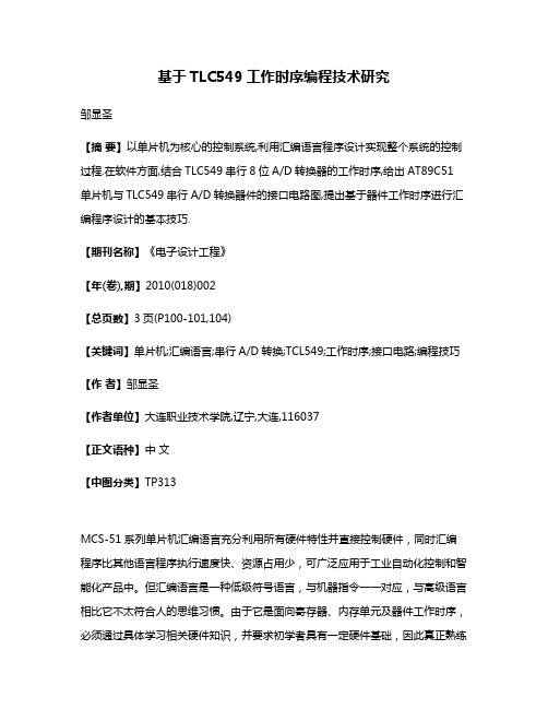
1 TLC549简介TLC549是8位串行A/D转换器,图1为其引脚配置。
图1 TCL549引脚配置它可与通用微处理器、控制器通过I/O CLOCK、CS、DATA OUT 3个引脚串行连接。
该器件有1个模拟输入端口ANALOG IN,三态数据串行输出接口可方便与微处理器或外围设备相连。
TLC549仅仅使用输入/输出时钟(I/O CLOCK)和片选信号()控制数据[3]。
TLC549有片内系统时钟,该时钟与I/O CLOCK独立工作,无需特殊速度或相位匹配,其工作时序如图2所示[4]。
图2 TLC549工作时序详细分析TLC549的工作时序得到如下信息[5]:1)串行数据中A7位先输出,A0位最后输出;2)在每一次I/O COLCK的高电平期间DATA OUT线上的数据产生有效输出,每出现一次I/O COLCK,DATA OUT线就输出1位数据。
- 1、下载文档前请自行甄别文档内容的完整性,平台不提供额外的编辑、内容补充、找答案等附加服务。
- 2、"仅部分预览"的文档,不可在线预览部分如存在完整性等问题,可反馈申请退款(可完整预览的文档不适用该条件!)。
- 3、如文档侵犯您的权益,请联系客服反馈,我们会尽快为您处理(人工客服工作时间:9:00-18:30)。
8位串行模数转换器TLC548、TLC549的应用1. 概述
TLC548,TLC549是美国德州仪器公司生产的8位串行A/D转换器芯片,可与通用微处理器、控制器通过CLK、CS、DATA OUT三条口线进行串行接口。
具有4MHz片内系统时钟和软、硬件控制电路,转换时间最长17μs,TLC548允许的最高转换速率为45 500次/s,TLC549为40 000次/s。
总失调误差最大为±0.5LSB,典型功耗值为6mW。
采用差分参考电压高阻输入,抗干扰,可按比例量程校准转换范围,V REF-接地,V REF+-V REF-≥1V,可用于较小信号的采样。
2. 芯片简介
2.1 TLC548、TLC549的内部框图和管脚名称
TLC548、TLC549的内部框图和引脚名称如图1所示。
2.2 极限参数
TLC548/549的极限参数如下:
●电源电压:6.5V;
●输入电压范围:0.3V~V CC+0.3V;
●输出电压范围:0.3V~V CC+0.3V;
●峰值输入电流(任一输入端):±10mA;
●总峰值输入电流(所有输入端):±30mA;
●工作温度:TLC548C、TLC549C:0℃~70℃
TLC548I、TLC549I:-40℃~85℃
TLC548M、TLC549M:-55℃~125℃
3. 工作原理
TLC548、TLC549均有片内系统时钟,该时钟与I/O CLOCK是独立工作的,无须特殊的速度或相位匹配。
其工作时序如图2所示。
当CS为高时,数据输出(DATA OUT)端处于高阻状态,此时I/O CLOCK 不起作用。
这种CS控制作用允许在同时使用多片TLC548、TLC549时,共用I/O CLOCK,以减少多路(片)A/D并用时的I/O控制端口。
一组通常的控制时序为:
(1)将CS置低。
内部电路在测得CS下降沿后,再等待两个内部时钟上升沿和一个下降沿后,然后确认这一变化,最后自动将前一次转换结果的最高位(D7)位输出到DATA OUT端上。
(2) 前四个I/O CLOCK周期的下降沿依次移出第2、3、4和第5个位(D6、D5、D4、D3),片上采样保持电路在第4个I/O CLOCK下降沿开始采样模拟输入。
(3)接下来的3个I/O CLOCK周期的下降沿移出第6、7、8(D2、D1、D0)个转换位,
(4)最后,片上采样保持电路在第8个I/O CLOCK周期的下降沿将移出第6、7、8(D2、D1、D0)个转换位。
保持功能将持续4个内部时钟周期,然后开始进行32个内部时钟周期的A/D转换。
第8个I/O CLOCK后,CS必须为高,或I/O CLOCK保持低电平,这种状态需要维持36个内部系统时钟周期以等待保持和转换工作的完成。
如果CS为低时I/O CLOCK上出现一个有效干扰脉冲,则微处理器/控制器将与器件的I/O时序失去同步;若CS为高时出现一次有效低电平,则将使引脚重新初始化,从而脱离原转换过程。
在36个内部系统时钟周期结束之前,实施步骤(1)-(4),可重新启动一次新的A/D转换,与此同时,正在进行的转换终止,此时的输出是前一次的转换结果而不是正在进行的转换结果。
若要在特定的时刻采样模拟信号,应使第8个I/O CLOCK时钟的下降沿与该时刻对应,因为芯片虽在第4个I/O CLOCK时钟下降沿开始采样,却在第8个I/O CLOCK的下降沿开始保存。
4. 应用接口及采样程序
TLC548、TLC549可方便地与具有串行外围接口(SPI)的单片机或微处理器配合使用,也可与51系列通用单片机连接使用。
与51系列单片机的接口如图3所示。
其采样程序框图如图4所示,实际应用程序清单如下:
初始化:
SETB P1.2 ;置CS为1。
CLR P1.0 ;置I/O CLOCK为零。
MOV R0,#00H ;移位计数为零。
A/D过程:
A/DP: CLR P1.2
NOP ;等待1.4μs,NOP数根据晶振情况选择
NXT: SETB P1.0
MOV C, P1.1
RLC A
CLR P1.0
INC R0
CJNE R0,#8,NXT
MOV R0,#00
SETB P1.2
MOV DTSVRM,A ;DTSVRM:DATA SAVE RAM.
RET
TLC548/549片型小,采样速度快,功耗低,价格便宜,控制简单。
适用于低功耗的袖珍仪器上的单路A/D或多路并联采样。