AD549中文PDF
杰克特腊斯 类型549分裂屏存储波形显示器说明书

TYPE 549SPLIT-SCREEN STORAGE OSCILLOSCOPE•BISTABLE SPLIT-SCREEN STORAGEAND CONVENTIONAL DISPLAYS•VARIABLE VIEW ING TIME•5cm/its W RITING SPEED•CALIBRATED SWEEP DELAY•FULL-BANDWIDTH TRIGGERING•ACCEPTS MULTI-TRACE, DIFFERENTIAL,SAMPLING, AND SPECTRUM ANALYZERPLUG-IN UNITSThe Type 549 extends the exclusive Tektronix split-screen and bistable storage features into research and development applications. Offering a high degree of versatility, it accepts all letter-series and 1-series plug-in units covering many applications including sampling and spectrum analysis.The split-screen, bistable CRT provides high contrast displays and unparalleled writing speeds. Each half of the 6x10-cm display area can be independently controlled, thus allowing stored or conventional displays on either the upper or lower half. A stored display can then be compared simultaneously with a conventional display.A variable-viewing-time system offers a new convenience to storage oscilloscope users. Through front panel controls, this system can be directed to automatically erase either or both halves of the display area after a predetermined viewing time. Viewing time can be varied from <0.5 seconds to >5seconds with AUTO ERASE selected for either PERIODIC or AFTERSWEEP operation. Used in conjunction with the SINGLE SWEEP, the "After-Sweep" erase circuit automatically resets the Single- Sweep circuit at the end of the viewing-time interval.CHARACTERISTIC SUMMARYVERTICALVertical deflection characteristics extremely flexible through use of all Letter-Series and 1-Series Plug-In Units.HORIZONTALCALIBRATED TIME BASE—0.1 /is/cm to 5s/cm.X5 MAGNIFIER—Extends time base to 20ns/cm. CALIBRATED SWEEP DELAY—2 /xs to 10 s.EXTERNAL INPUT—0.2 V/cm, DC to 350 kHz.STORAGE CRTDISPLAY AREA—6x10 cm.SPLIT SCREEN STORAGE—Store on either upper or lower half of screen with non-storage on other half; store on entire screen; or non-store on entire screen.LOCATE ZONE—Locate button permits vertical position finding. VIEW ING TIME—Up to one hour.ERASE TIME—150 ms maximum.WRITING SPEED—0.5cm/^s. 5 cm//j.s with enhancement.PHO SPHOR-PIOTHERAMPLITUDE CALIBRATOR—0.2 mV to 100 V; 5 mA current loop; 1kHz.POWER REQUIREMENTS—104, 115, 127, or 208, 230, and 254 volts, center value (regulation range ±10%), 650 W (approx) maximum.108TYPE549AVAILABLE DISPLAYSWith the wide range of vertical plug-in units, several types of stored and conventional displays are obtainable. The Type 549, by virtue of a new bistable split-screen storage CRT capable of unparalleled writing speeds, extends storage-measuring capability into previously unattainable areas.SINGLE-TRACE AND MULTI-TRACEMulti-trace displays are obtained by selecting a Type 1A1, 1A2, 1A4, CA, or M Amplifier Plug-In Unit. All other 1-Series and Letter-Series Plug-In Units will give single-trace displays. Selection of the Type 1A5, 1A6, 1A7, D, E , or G gives differential amplifier operation, while strain gage and other transducer operations are available with the Type Q Unit. SAMPLINGSampling displays with risetimes in the sub-nanosecond region are obtained using a Type 1S 1 or 1S2 Sampling Unit. The Type 1S 1 is a general-purpose sampler with 1 GHz bandwidth, delay line and internal triggering. The Type 1S2 is designed specifically for TDR (time-domain reflectometry) applications, but offers general-purpose sampling with 3.9 GHz bandwidth and built-in triggering.SPECTRUM ANALYSISSpectral displays are obtained using a Type 1 L5, 1L10, 1L20, or 1L30 Spectrum Analyzer Plug-In Unit to cover a frequency range from 10 Hz to 10.5 GHz.There are decided advantages in using the storage oscilloscope for spectrum analysis. When slow sweep times are used, it is often difficult to view a complete display; however, by storing the display it can be completely and easily observed.Signal drift is easily measured using the storage technique. The signal is stored and then as subsequent displays are stored, drift of the signal can be observed. Or, the spectral display can be stored on one half of the screen and simply compared with a similar non-stored display on the other.STORAGE CRT AND DISPLAY FEATURESSTORAGE CRTDirect viewing, bistable, split-screen, mono-accelerating with 4-kV accelerating potential and separate non-store "locate zone". External edge-lighted graticule. Tektronix bistable storage offers: 1) Brightness of a stored trace independent of viewing time; 2) Contrast of a stored trace independent of viewing time; and 3) Brightness of a stored trace independent of writing speed.DISPLAY AREA6x l0-c m split-screen storage area with independent or common control, plus locate zone.LIF E CHARACTERISTICSThe aging rate of the storage target depends upon the mode of use. The above chart shows typical brightness aging characteristics when the target is used continuously in STORE mocfe.SPLIT-SCREEN STORAGEStore on either upper or lower half of screen with conventional display on other half; store on entire screen; or, nonstore on entire screen. Independent operation of both halves.VIEW ING TIMEUp to one hour. If ENHANCE MODE is to be used, it is recommended that displays be stored for 20 minutes or less.ENHANCE MODEControls the single sweep storage capabilities of the storage CRT. Through adjustment of ENHANCE LEVEL control, singletrace spot velocities up to 5 cm//xs or better can be stored with minimal loss of resolution and contrast.LOCATE BUTTON (Serves two functions)STORAGE—When depressed, the beam appears at the left of the CRT screen marking the vertical position of the next sweep. CONVENTIONAL DISPLAYS—Permits beam finding of off screen signals.ERASE TIME150 ms maximum.AUTO ERASE SYSTEMViewing time before erase continuously variable from <0.5 s to >5 s.In the PERIODIC Mode, there is a continuous sequence of storing, viewing time and erasure. This sequence occurs regardless of whether or not a signal is present and is independent of the sweep. In the AFTER SWEEP mode—which is used in conjunction with the SINGLE SWEEP—the sequence begins with the arrival of the signal. The signal initiates a sweep by triggering the Single Sweep circuitry. Viewing time begins as the sweep ends. At the end of the viewing time, erasure automatically resets the SINGLE SWEEP, readying it for the next signal. This cycle will automatically repeat itself as long as a signal is available.Manual control available through Erase and Reset button or by Reset position of Single Sweep switch.REMOTE CONTROL OPERATIONThe Type 549 has remote control-operation capabilities using contact closure. A 9-pin connector, located on the rear panel, supplies one ground and 7 inputs (plus one spare) that allows the following functions:1. Remote erase of upper screen.2. Remote erase of lower screen.3. Remote resetting of sweep for single-sweep operation.4. Remote erase of both halves of the screen and resetting of the sweep.5. Remote switching from conventional operation to storage operation (independently or commonly) of upper or lower screen halves.6. Remote interruption of the Auto Erase sequence in order to hold a stored waveform.Operation of these circuits is achieved by grounding the appropriate pin in the connector.REMOTE CONTROL UNIT(Optional accessory, part number 012-0102-00). Performs Remote Erase and Reset functions numbers 1, 2, and 3 above.Z-AXIS INPUTA CRT grid selector switch on the rear panel allows the CRT grid to be driven from the internal unblanking signal, or from an external source. Bandpass is DC to >1 MHz at —3dB. 20 V peak to peak required for beam modulation. Input R C is lOOkO and 80 pF. A CRT CATHODE-SELECTOR switch allows the cathode to be driven from the internal chopped- blanking signal, or from an external source, AC coupled. 20 V peak to peak required for beam modulation at normal intensity.109VERTICAL DEFLECTIONTYPE549VERTICAL PLUG-IN UNITS PLUG-IN M INIM U M BANDWIDTH t rUNITDEFLECTION (-3 dB)FACTORMULTIPLE TRACE1A 150 mV/cm DC to 30 MHz 12 n s Dual-Trace 5 mV/cm DC to 23 MHz 16 n s ~500 /iV/cm 2 Hz to 14 MHz 25 n s 1A2Dual-Trace 50 mV/cm DC to 30 MHz 12 n s CADual-Trace 50 mV/cm DC to 23 MHz 16 n s 1A4Four-Trace 10 mV/cm DC to 30 MHz 12 n s MFour-Trace20 mV/cmDC to 19 MHz19 n sSINGLE TRACEB 50 mV/cm DC to 18 MHz 20 n s 5 mV/cm 2 Hz to 12 MHz 30 n s H 5 mV/cm DC to 14 MHz 25 n s K 50 mV/cm DC to 27 MHz 13 n s L50 mV/cm DC to 27 MHz 13 n s 5 mV/cm3 Hz to 23 MHz16 n sSPECIAL PURPOSEOOperational 50 mV/cm DC to 23 MHz 16 n s QStrain Gage10 /xstrain/aivDC to 6 kHz60 /isDIFFERENTIAL1A55 mV/cm DC to 30 MHz 12 n s Comparator 2 mV/cm DC to 29 MHz 13 n s 1 mV/cm DC to 28 MHz 13 n s 1A61 mV/cm DC to 2 MHz 0.18 /is 1A7A10 /xV/cm DC to 1 MHz 350 n sHigh-Gain Selectable D 1 mV/cmDC to 300 kHz (to 50 mV/cm)(DC to 2 MHz)0.18 /x s E50 /iV/cm0.06 Hz to 20 kHz (to 10 mV/cm)[to 60 kHz) Selectable6 /x s G 50 mV/cm DC to 18 MHz 20 n s W1 mV/cm DC to 7 MHz 50 n s Comparator 50 mV/cm DC to 22 MHz 16 n s ZComparator50 mV/cmDC to 13 MHz27 n sSPECTRUM ANALYZERS1L510 /iV/cm 10 Hz to 1 MHz 1 LI 0-100 dBm 1 MHz to 36 MHz 1L20— 110 to —90 dBm 10 MHz to 4.2 GHz 1L30— 105 to —75 dBm 925 MHz to 10.5 GHzW IDE-BAND SAMPLING1S 12 mV/cm DC to 1 GHz350 p s 1S 2 TD R5 mp/cm 140 ps system risetime 5 mV/cmDC to 3.9 GHz 90 p sBANDWIDTHDC to >30 MHz at 3-dB down, depending on plug-in unit. See chart.RISETIME<12 ns, depending on plug-in unit. See chart.DELAY LINEPerrfiits viewing leading edge of displayed waveform.SIGNAL OUTPUTDC to >5 MHz at 3-dB down, <70 ns risetime, 1.5 V ±20% for each centimeter of displayed signal.HORIZONTAL DEFLECTIONTIME BASE A0.1 /xs/cm to 5s/cm in 24 calibrated steps (1-2-5 sequence), accurate within 3%. Uncalibrated, continuously variable between steps and to approx 12.5s/cm. Warning light indicates uncalibrated setting.TIME BASE B 2/xs/cm to 1 s/cm in 18 calibrated steps (1-2-5 sequence), accurate within 3%. Sweep length variable from 4 to 10 cm, allowing use of Time Base B as a repetition-rate generator from 0.1 Hz to 40 kHz.X5 MAGNIFIEROperates over full time base, increases fastest Time Base A rate to 20ns/cm, and the fastest Time Base B rate to 0.4/is/ cm. Magnified time base accurate within 5%.DELAY TIME2/xs to 10 s, continuously variable and calibrated, accurate within 1 % of indicated delay ±2 minor divisions. Add processing time of 200 ns at fast sweep rates. Incremental delay-time accurate within 1% ±4 minor divisions. Shortterm jitter <1 part in 20,000 of the available delay time.DELAY MODESDepending on the setting of the Delayed Sweep stability control, the Delayed Sweep can start immediately at end of delay time, or be triggerable at end of delay time (for jitter- free displays).OPERATING MODESTime Base A, Time Base B , B intensified by A, and A delayed by B . Single sweep in any mode; reset accomplished with ERASE and R ESET button on front panel, NORMAL-SINGLE SWEEP-RESET switch on front panel, automatically with AUTO ERASE switch in AFTER SWEEP and NORMAL-SINGLE SWEB>- R E S E T switch in SINGLE SWEEP, or by remote control through rear-panel connector.EXTERNAL INPUTFixed steps of approx 0.2V/cm and 2V /cm , continuously variable between steps and to approx 20V/cm , DC to >350 kHz at —3 dB with maximum gain. 600 V maximum input (DC + peak AC). Input RC approx 1 M fi paralleled by <60 pF.SIGNAL OUTPUTSGates from both time bases (0 to at least +20 V), sawtooth from Time Base A (0 to at least +130V ), and a delayed trigger pulse (at least +5 V).110TYPE 549STORED5c m/ix s SINGLE-SWEEP W RITING SPEEDUpper display shows a single shot 625-kHz sinewave storedin enhanced mode of operation. Sweep time is 1ps/cm.FAST REPETITIVE DISPLAYLower display is a recurrent, 1-MHz squarewave with a risetime of 20 ns stored without enhancement. Sweep timeis 0.1 ps/cm.DISPLAYSFREQUENCY-BASED DISPLAYHarmonic analysis of simulated 440-Hz oboe tone [upperIand violin (lower screen). Dispersion is 500Hz/cm; minimum resolution bandwidth. Zero-frequency feedthroughis displayed in the first centimeter.TRIGGERMODESAutomatic or manual level selection. Automatic operation is useful between approx 50 Hz and 1MHz, minimizes trigger adjustments for signals of different amplitudes, shapes, and repetition rates. With no input (or input less than 50 Hz), automatic triggering occurs at an approx 50-Hz rate, providing a convenient reference trace.COUPLINGAC, DC, or AC L F reject.SOURCESInternal from oscilloscope vertical amplifier (or direct from a single channel of Type 1A1, 1A2 or 1A4 Plug-In Units), external, or line. 50-V maximum external input (DC +peak AC).TIME BASE A REQUIREMENTS02-cm deflection or 0.3-V external from DC to 10 MHz, increasing to 2-cm deflection or 3-V external at 30MHz. Requirements increase below 300 Hz with AC coupling, below 200 kHz with AC low-frequency reject. Automatic operation requires 0.2-cm deflection or 0.3-V external from 300 Hz to10 kHz, increasing to 2-cm deflection or 3-V external at 1MHz. TIME BASE B REQUIREMENTS02-cm deflection or 0.3-V external from DC to 1MHz, increasing to 1-cm deflection or 1.5-V external at 10 MHz.Requirements increase below 300 Hz with AC coupling, below 200 kHz with AC low-frequency reject__Automatic operation requires 0.2-cm deflection or 0.3-V external from 300 Hz to10 kHz, increasing to 2-cm deflection or 3-V external at 1MHz.OTHER CHARACTERISTICSAMPLITUDE CALIBRATOR0.2 mV to 100 V squarewave, 18 calibrated steps (1-2-5 sequence), accurate within 2%. 50-0 ±2%source resistance from 0.2 mV to 0.2 V. Stl-jus risetime; 1-kHz ±25%repetition rate; 40% to 60% duty cycle. 100-V DC reference output also provided. Front-panel current loop for 5 mA ±2%, squarewave or DC.POWER REQUIREMENTSWired for 115 V RMS ±10%; rear-panel and internal switches permit operation at 104, 115, 127, 208, 230, or 254 V (±10%on each range); 50 to 60 Hz source having less than 2% harmonic distortion. Approx 650 W maximum power consumption, approx 750 VA maximum.DIMENSIONS AND WEIGHTSHeight17 in43.2 cm Width12’Vu in32.9 cm Depth23% in60.7 cm Net weight67% lb30.8 kg Domestic shipping weight~89 lb~40.5 kg Export-packed weight~114 lb~51.8 kg INCLUDED STANDARD ACCESSORIESTwo P6006 10X probes (010-0127-00); two BNC-to-BNC 18-in patch cords (012-0087-00); BNC-to-binding post adapter (103- 0033-00); 3 to 2-wire adapter (103-0013-00); 3-conductor power cord (161-0010-03); smoke-gray light filter (378-0567-00); two instruction manuals (070-0508-00).I llTYPE 549OPTIONAL ACCESSORIESOptional accessories increase measurement capability and provide added convenience. Cameras, probes, Scope-Mobile® Carts and other major accessories are completely described in the catalog accessory pages.CAMERAThe standard C-12 camera satisfies most trace-recording requirements. For applications that might require a different viewing system, lens, or back, refer to camera descriptions or consult your field engineer, representative, or distributor. Standard C-12: f/1.9—1:0.85 lens, no-parallax viewing, Polaroid Land* Pack-Film backType 549 to C-12 Camera adapter, order 016-0226-00PROBESThe standard 10X probes supplied with the instrument satisfy most measurement requirements; however, optional probes (recommended on plug-in unit pages) may be better suited for particular applications.SCOPE-MOBILE® CARTModel 202-2: storage drawer, carrier for 2 plug-in units, 9- position tilt-lock oscilloscope trayTV ACCESSORIES FOR GENERAL-PURPOSE OSCILLOSCOPES In addition to the Tektronix line of television instruments, accessories are available for use with many Tektronix general- purpose oscilloscopes. A TV Sync Separator provides stable triggering for the display of composite video signals. A Video Staircase Differentiator allows the amplitude linearity of television systems and their components to be measured. See the catalog accessory pages for additional information.REMOTE-CONTROL UNITSeparate controls for erase of upper screen, erase of lower screen, and single-sweep reset. Mates to oscilloscope rear-panel connector, 9-foot cable, order 012-0102-00 REMOTE-CONTROL CONNECTOR9-pin cable connector for 5 erase and reset functions plus selection of storage or non-storage operation. Mates to oscilloscope rear-panel connector. Cable and control unit not included, order 134-0049-00RACK-MOUNT ADAPTERConsists af cradle to support the Type 549 in any standard 19-in relay rack, and mask to fit around the front panel.Requires 17V2-in panel height, order 040-0281-00*Registered Trade-Mark Polaroid CorporationPlease refer to Terms and Shipment, General Information page.112。
AD56xx AD568xx-R NanoDAC+ Data Sheet说明书

Rev. 0Information furnished by Analog Devices is believed to be accurate and reliable. However, noresponsibility is assumed by Analog Devices for its use, nor for any infringements of patents or other rights of third parties that may result from its use. Speci cations subject to change without notice. No license is granted by implication or otherwise under any patent or patent rights of Analog Devices. T rademarks and registered trademarks are the property of their respective owners. One Technology Way, P.O. Box 9106, Norwood, MA 02062-9106, U.S.A. Tel: 781.329.4700 Fax: 781.461.3113 ©2012 Analog Devices, Inc. All rights reserved.功能框图表1. 四通道nanoDAC+器件接口代号16位14位12位SPI 内部AD5686R AD5685R AD5684R外部AD5686AD5684I2C 内部AD5696R AD5695R AD5694R外部AD5696AD5694 SCLV LOGICSDAA1A0INPUTREGISTERDACREGISTERSTRINGDAC ABUFFERV OUT AINPUTREGISTERDACREGISTERSTRINGDAC BBUFFERV OUT BINPUTREGISTERDACREGISTERSTRINGDAC CBUFFERV OUT CINPUTREGISTERDACREGISTERSTRINGDAC DBUFFERV OUT DV REFGNDV DDPOWER-DOWNLOGICPOWER-ONRESETGAIN =×1/×2INTERFACELOGICRSTSEL GAINLDAC RESETAD5696/AD56941799-1四通道、16/12位nanoDAC+,集成I2C接口AD5696/AD5694产品特性高相对精度(INL):16位时最大±2 LSB小型封装:3 mm × 3 mm、16引脚LFCSP总不可调整误差(TUE):±0.1% FSR(最大值)失调误差:±1.5 mV(最大值)增益误差:±0.1% FSR(最大值)高驱动能力:20 mA,0.5 V(供电轨)用户可选增益:1或2(GAIN引脚)复位到零电平或中间电平(RSTSEL引脚)1.8 V逻辑兼容400 kHz I2C兼容型串行接口4个可用I2C地址低毛刺:0.5 nV-s鲁棒的HBM(额定值为3.5 kV)和FICDM ESD(额定值为1.5 kV)性能低功耗:1.8 mW (3 V)2.7 V至5.5 V电源供电温度范围:−40°C至+105°C应用数字增益和失调电压调整可编程衰减器过程控制(PLC I/O卡)工业自动化数据采集系统概述AD5696和AD5694均属于nano DAC+™系列,分别是低功耗、四通道、16/12位缓冲电压输出DAC,内置增益选择引脚,满量程输出为2.5 V(增益 = 1)或5 V(增益 = 2)。
LC549中文资料

LC549/LV549/LD549 DATA SHEETHigh Power Class BOutput StageFEATURES•40dB of electrical gain• 1.0 to 1.6 VDC supply operating range •current trim capability (R T )•high efficiency class B output stage•may be used with a linear or compression preamplfier STANDARD PACKAGING •8 pin MICROpac (LC549)•8 pin MINIpac•8 pin PLID ® (LC549, LD549)•Chip (47 x 40 mils) (LC549, LD549)DESCRIPTIONThe LC/LV/LD549 is an 8 pin, low voltage, push-pull audio frequency output stage amplifier with a single unbalanced input. The circuit utilizes two internal negative feedback loops to stabilize the DC operating point for temperature stability and to linearize the transfer function over a wide dynamic range. The circuit operates near ideal class B conditions resulting in low distortion and very low quiescent current, required for extended battery life.The LC549, LV549 and LD549 differ in only one respect;the LV549 and LD549 are selected devices which are capable of delivering from 10 mA to 41 mA and from 36 mA to 75 mA of output current respectively. These values are the maximum current drawn with both output stage transistors in saturation. Thus the LD549 is capable of producing a high output in a low impedance load, the LV549 is selected to have lower peak currents, extending the life of the battery.U.S. Patent No. 4,085,382Patented in other countriesBLOCK DIAGRAMR T V BINPUTDEC 1 DEC 2GNDGENNUM CORPORATION P.O. Box 489, Stn A, Burlington, Ontario, Canada L7R 3Y3 tel. (905) 632-2996 fax: (905) 632-5946Japan Branch: A-302 Miyamae Village, 2-10-42 Miyamae, Suginami-ku Tokyo 168, Japan tel. (03) 3334-7700 fax: (03) 3247-8839Document No. 500 - 25 - 09Revision Date: January 20012500 - 25 - 09SEQUENCE CONDITIONS COMMENTS 1 Power Supply Off 2S1Closed Removes V IN3S2 / S3Closed Discharges C2 and C34 S1Open Applies V IN (V IN level is determined from Gain Test) 5S2 / S3Open Removes short from C2 and C36Power SupplyOn7Gain must be within specification, within 3 seconds after power supply is turned onABSOLUTE MAXIMUM RATINGSPARAMETER VALUE & UNITSSupply Voltage 3 VDC Power dissipation 60 mWOperating Temperature -10 to + 40 °C Storage Temperature-20 to + 70 °CPIN CONNECTIONR T I/P DEC2V B GNDOUT1OUT2ELECTRICAL CHARACTERISTICSConditions: Temperature 25 o C, Supply Voltage V B = 1.3 VDCAll switches and parameters remain as shown in test circuit unless stated in condition columnPARAMETER SYMBOL CONDITION MIN TYP MAX UNITSGainA CL V OUT = 0.707 V RMS384042dB Quiescent CurrentI AMP 100-400µA I TRANS 170-370µA I TOT-500770µAMaximum Drive CurrentV1 = 0V (S2, S3 closed)V4 = 0V LC549103575mA LV54910-41mA LD549365075mA Input Impedance182736k ΩTotal Harmonic Distortion & NoiseTHDV OUT = 0.707 V RMS -0.5-%V OUT = 1.3 V RMS- 2.5 5.2%Input Referred Noise IRN NFB 0.2 to 10 kHz at 12 dB/oct (S1 closed)- 1.2 2.5µV Start Up Time--3secSTART-UP TIME TEST (Refer to Test Circuit)3500 - 25 - 09Fig. 1 Test CircuitAll resistors in ohms, all capacitors in farads unless otherwise stated U.S. Patent No. 4,085,382 - Patented in other countriesFig. 2 Equivalent CircuitV = R T = 600Ω1kHzAll resistors in ohms, all capacitors in µF unless otherwise statedGain = 20 Log 10( ) +40 dB VOUT VIN=∞4500 - 25 - 09V B=1.3VDCMICTEMPERATURE °CFig. 4 Volume Gain vs Battery VoltageFig. 5 Quiescent Current vs Battery VoltageFig. 6 Quiescent Current vs TemperatureFig. 7 Gain vs Temperature-20 -10 0 10 20 30 40 50 60 7041.040.239.438.637.837.0464442403836A V (dB )V B (V)V B (V)I Q (µA )I Q (µA )-20 -10 0 10 20 30 40 50 60 70TEMPERATURE (°C)A V (dB )8007006005004003000.9 1.0 1.1 1.2 1.3 1.4 1.5 1.6 1.7 1.85325245165085004920.9 1.0 1.1 1.2 1.3 1.4 1.5 1.6 1.7 1.85500 - 25 - 09R E L A T I V E V O L T A G E G A I N (d B )Gennum Corporation assumes no responsibility for the use of any circuits described herein and makes no representations that they are free from patent infringement.© Copyright January 1981 Gennum Corporation. All rights reserved. Printed in Canada.P O W E R O U T P U T (m V )I Q (µA )A V (d B)0 4 8 12 16 20 24 260.01 0.1 1.0 10 10012108642LDLC-0 200 400 600 800 1k41403938373640.440.240.039.839.6550500450400350300250200LOAD R L (Ω)FREQUENCY (kHZ)Fig. 9 Voltage Gain vs FrequencyFig. 8 Power Output vs Load Resistance at 7% Distortion R B = 0Ω1 10 100 1KSUPPLY VOLTAGE (V)Fig. 11 Voltage Gain vs Battery ResistanceFig. 10 Quiescent Current vs Current Trim Resistor R T(k Ω)DOCUMENT IDENTIFICATIONPRODUCT PROPOSALThis data has been compiled for market investigation purposes only, and does not constitute an offer for sale.ADVANCE INFORMATION NOTEThe product is in a development phase and specifications are subject to change without notice. Gennum reserves the right to remove the product at any time. Listing the product does not constitute an offer for sale.PRELIMINARY DATA SHEETThe product is in preproduction phase and specifications are subject to change without notice.DATA SHEETThe product is in production. Gennum reserves the right to make changes at any time to improve reliability, function or design, in order to provide the best product possible.。
OPA549T中文资料

q HIGH OUTPUT CURRENT: 8A Continuous 10A Peak q WIDE POWER SUPPLY RANGE: Single Supply: +8V to +60V Dual Supply: ±4V to ±30V q WIDE OUTPUT VOLTAGE SWING q FULLY PROTECTED: Thermal Shutdown Adjustable Current Limit q OUTPUT DISABLE CONTROL q THERMAL SHUTDOWN INDICATOR q HIGH SLEW RATE: 9V/µs q CONTROL REFERENCE PIN q 11-LEAD POWER ZIP PACKAGE
±20
25 –100 ±0.5 ±5 70 1 (V+) – 2.3 (V–) – 0.2 95 107 || 6 109 || 4
INPUT VOLTAGE RANGE Common-Mode Voltage Range: Positive VCM Negative VCM Common-Mode Rejection Ratio CMRR INPUT IMPEDANCE Differential Common-Mode OPEN-LOOP GAIN Open-Loop Voltage Gain FREQUENCY RESPONSE Gain Bandwidth Product Slew Rate Full Power Bandwidth Settling Time: ±0.1% Total Harmonic Distortion + Noise(3) AOL
VO = ±25V, RL = 1kΩ VO = ±25V, RL = 4Ω
Latitude 5490 快速入门指南.pdf_1700877421.9748924说明书

1Connect the power adapter and press the power buttonTilslut strømadapteren, og tryk på tænd/sluk-knappen Kytke verkkolaite ja paina virtapainikettaKoble til strømadapteren og trykk på strømknappenAnslut nätadaptern och tryck på strömbrytarenProduct support and manuals Support og manualer til produktet Tuotetuki ja oppaatProduktstøtte og håndbøker Produktsupport och handböcker /support/support/manuals /support/windowsContact DellKontakt Dell | Ota yhteyttä Delliin Kontakt Dell | Kontakta Dell/contactdellRegulatory and safetyLovbestemmelser og sikkerhed | Säädökset ja turvallisuus Bestemmelser og sikkerhet | Föreskrifter och säkerhet /regulatory_complianceRegulatory modelLovmodel | SäädösmalliForskriftsmodell | Regelmodell P72GRegulatory typeLovbestemmelsestype | Säädöstyyppi Forskriftstype | RegeltypP72G002Computer modelComputermodel | Tietokoneen malli Datamaskinmodell | DatormodellLatitude-54902017-11What’s NewNyheder | UuttaHva er nytt | Nyheter• Supports Dual (7th Gen Intel Core) and Quad (8th Gen Intel Core) processors• Supports up to 2400 MHz DDR4 memory with 8th Gen Intel Core processors• Understøtter Dual Core- (7. generation Intel Core) og Quad Core-processorer (8. generation Intel Core)• Understøtter op til 2400 MHz DDR4-hukommelse med 8. generations Intel Core-processorer• Tuki Dual-suorittimille (7. sukupolven Intel Core) ja Quad-suorittimille (8. sukupolven Intel Core)• Tuki jopa 2 400 MHz DDR4 -muistille 8. sukupolven Intel Core-suorittimilla • Støtter to (7. generasjons Intel Core) og fire (8. generasjons Intel Core) prosessorer• Støtter opptil 2400 MHz DDR4-minne med 8. generasjons Intel Core-prosessorer• Stöd för dubbla processorer (7:e generationens processorer av typen Intel Core) och fyra processorer (8:e generationens processorer av typen Intel Core)• Stöder upp till 2 400 MHz DDR4-minne med 8:e generationens processorer av typen Intel Core© 2017 Dell Inc. or its subsidiaries.© 2017 Intel Corporation.FeaturesFunktioner | Ominaisuudet | Funksjoner | Funktioner16. USB 3.1 Gen 1 port with PowerShare17. Headset/Microphone port18. Touch Fingerprint reader (optional)19. Battery charge status light20. Contactless card reader (optional)21. Speakers22. Touchpad23. Smart card reader (optional)24. Pointstick (optional)25. SD card reader26. USB 3.1 Gen 1 port27. DisplayPort over USB Type-C28. Microphone status light29. Service Tag label1. Netværksport2. Kamera3. Statusindikator for kamera4. microSIM-kortslot (valgfrit tilbehør)5. HDMI-port6. USB 3.1 Gen 1-port7. Strømstikport8. Infrarød sender (valgfrit tilbehør)9. Infrarødt kamera (valgfrit tilbehør)10. Kamera (valgfrit tilbehør)11. Kamerastatusindikator (valgfrittilbehør)12. To arraymikrofoner13. Indikator for tænd/sluk-knap/strømstatus14. Noble Wedge-låseslot15. VGA-port16. USB 3.1 Gen 1-port med PowerShare17. Hovedtelefon-/mikrofonport18. Fingeraftrykslæser medberøringsskærm (valgfrit tilbehør)19. Indikator for batteriopladningsstatus20. Kontaktfri kortlæser (valgfrittilbehør)21. Højttalere22. Berøringsplade23. Chipkortlæser (valgfrit tilbehør)24. Pegepind (valgfrit tilbehør)25. SD-kortlæser26. USB 3.1 Gen 1-port27. DisplayPort over USB Type-C28. Indikator for mikrofonstatus29. Servicekode1. Verkkoportti2. Kamera3. Kameran tilavalo4. micro-SIM-korttipaikka (valinnainen)5. HDMI-portti6. USB 3.1 Gen 1 -portti7. Virtaliitäntä8. Infrapunalähetin (IR) (lisävaruste)9. Infrapunakamera (IR) (lisävaruste)10. Kamera (valinnainen)11. Kameran tilavalo (valinnainen)12. Kaksi mikrofonia13. Virtanäppäin / virran tilan LED14. Nobel-lukkopaikka15. VGA-portti16. USB 3.1 Gen 1 -portti, jossaPowerShare17. Kuuloke-/mikrofoniliitäntä18. Sormenjäljenlukija (valinnainen)19. Akun lataustilan valo20. Kontaktiton kortinlukija (valinnainen)21. Kaiuttimet22. Kosketuslevy23. Älykortinlukija (lisävaruste)24. Tappihiiri (valinnainen)25. SD-kortinlukija26. USB 3.1 Gen 1 -portti27. DisplayPort USB Type-C:n kautta28. Mikrofonin tilan merkkivalo29. Huoltomerkkitarra1. Nettverksport2. Kamera3. Statuslampe for kamera4. Spor til mikroSIM-kort (valgfritt)5. HDMI-port6. USB 3.1 Gen 1-port7. Strømkontaktport8. Infrarød (IR) sender (tilleggsutstyr)9. Infrarødt (IR) kamera(tilleggsutstyr)10. Kamera (valgfritt)11. Kamerastatuslys (valgfritt)12. Dobbel-array-mikrofoner13. LED for strømknapp/strømstatus14. Noble Wedge-låsspor15. VGA-port16. USB 3.1 Gen 1-port medPowerShare17. Hodesett-/mikrofonport18. Fingeravtrykksleser medberøringsfunksjon (tilleggsutstyr)19. Ladestatuslys20. Kontaktløs kortleser (tilleggsutstyr)21. Høyttalere22. Styreplate23. Smartkortleser (tilleggsutstyr)24. Styrepinne (tilleggsutstyr)25. SD-kortleser26. USB 3.1 Gen 1-port27. DisplayPort over USB Type-C28. Statuslampe for mikrofon29. Etikett med servicemerke1. Nätverksport2. Kamera3. Statuslampa för kamera4. Micro-SIM-kortplats (tillval)5. HDMI-port6. USB 3.1-port Gen 17. Port för nätanslutning8. Infraröd (IR) sändare (tillval)9. Infraröd kamera (IR) (tillval)10. Kamera (tillval)11. Kamerastatuslampa (tillval)12. Dubbla mikrofoner13. Strömbrytare/batteristatuslampa14. Plats för Noble-killås15. VGA-port16. USB 3.1-port Gen 1 medPowerShare17. Headset-/mikrofonport18. Fingeravtrycksläsare medpekfunktion (tillval)19. Lampa för batteriladdningsstatus20. Kontaktlös kortläsare (tillval)21. Högtalare22. Pekskiva23. Smartkortläsare (tillval)24. Pointstick (tillval)25. SD-kortläsare26. USB 3.1-port Gen 127. DisplayPort över USB Type-C28. Statuslampa för mikrofon29. Serviceetikett。
AD5439中文资料

SDO为输出,用以查看寄存器的内容加电时寄存器清零复位,输出为零参考电压Vref输入范围+/-10VVdd为电源电压2.5V-5.5V输出电压建立时间最大值110ns,典型值55ns数字量输入电压最大值Vih为1.7V 最小值Vil为0.8V 数据延时最大值40ns,典型值20ns时钟输入SCLK ,其频率最大值f sclk为50MHz数据输入时序如下:在SCLK 上升沿到来时,数据被锁存到输入移位寄存器当中 逻辑输入电压范围是-0.3V 到Vdd+0.3V如果FPGA 输入高电平电压是5V 时,Vdd 接5V 电源如果FPGA 输入高电平电压是3.3V 时,Vdd 接3.3V 电源 0ns各个管脚功能描述如下:1脚I out1A DAC A电流输出2脚I out2A DAC A 模拟地,此脚要接入系统模拟地,但可根据电源供电方式而有所不同3脚R FBA反馈电阻引脚,通过连接到外部的放大器输出端,建立起DAC A的电压输出4脚V REFA DAC A的参考输入电压5脚GND接地引脚6脚/LDAC 加载DAC 写信号输入,允许DAC输出的同步或异步更新。
当/LDAC由高变低时,DAC将处于异步更新。
而当/LDAC一直为低电平时,在芯片处于独立模式下,DAC将在第16个时钟SCLK的下降沿同步更新,或在器件处于串级链模式下将在/SYNC信号的上升沿同步更新7脚SCLK 时钟信号输入,默认情况下,数据将在SCLK的下降沿锁存到输入移位寄存器,也可通过控制位使数据在SCLK的上升沿锁存到输入移位寄存器8脚SDIN 串行数据输入端,在时钟SCLK有效边沿时,数据将锁存到16位输入寄存器中。
默认情况下,在上电复位时,数据将在时钟SCLK下降沿时输入到输入移位寄存器,也可通过控制位改变时钟SCLK有效边沿9脚SDO 串行数据输出,默认情况下,数据是在时钟SCLK下降沿时输入到输入移位寄存器,而在接下来的时钟SCLK上升沿通过SDO输出。
tcl549翻译

tcl549翻译TLC549 8bit 模数转换和串行控制●微处理器外设和独立操作●8bit分辨率A/D转换●差分参考输入电压●转化时间最大…17us●每秒访问总次数和转换周期:TCL549 (40000)●片上软件控制器,采样和保持●最大误差…±0.5LSB●4M内部系统时钟●电源电压范围…3-6V●低功耗…最大15mW●理想的高性价比,高性能的应用,包括电池供电的便携式仪表。
●引脚和控制信号与TLC540和TLC545 8位A / D转换器以及TLC1540 10位A / D转换器兼容描述TLC548和TLC549是围绕8位开关电容逐次逼近型ADC构建的CMOS模数转换器(ADC)集成电路。
这个器件设计用于通过3态数据输出和模拟输入与微处理器或外设进行串行接口。
TLC548和TLC549使用I/O CLOCK以及片选(CS)输入进行数据控制。
TLC548的最大I/O CLOCK输入频率为2.048 MHz,TLC549的I/O CLOCK输入频率为1.1 MHz。
TLC548和TLC549的操作与更复杂的TLC540和TLC541设备的操作非常相似;然而,TLC548和TLC549提供片上系统时钟,通常工作在4 MHz,无需外部元件。
片内系统时钟允许内部器件操作独立于串行输入/输出数据定时进行,并允许按照所需的软件和硬件要求操作TLC548和TLC549。
I/O CLOCK 与内部系统时钟允许TLC548的高速数据传输和每秒45500次转换的转换速率,以及TLC549的每秒40000次转换。
另外TLC548和TLC549的特征包括多功能控制逻辑,可在微处理器控制下工作的片上采样保持电路,以及具有差分高阻参考电压输入的高速转换器用来简化比例转换,缩放,独立的逻辑电路抑制噪声。
完全开关电容逐次逼近型转换器电路的设计允许在小于17μs 的时间内实现±0.5最低有效位(LSB )的最大总误差转换。
AD546资料

*Covered by Patent No. 4,639,683.
REV. A
Information furnished by Analog Devices is believed to be accurate and reliable. However, no responsibility is assumed by Analog Devices for its use, nor for any infringements of patents or other rights of third parties which may result from its use. No license is granted by implication or otherwise under any patent or patent rights of Analog Devices.
Conditions
VCM = 0 V VCM = ± 10 V VCM = 0 V VCM = ± 10 V VCM = 0 V VCM = 0 V
TMIN–TMAX
AD546J
AD546K
Min Typ Max Min Typ Max
0.2 1 0.1 1
40 40 0.17
13
0.2
0.5
0.2
80
76
–12
ad549中文资料

极低偏置电流运算放大器AD5491 概述AD549是具有极低输入偏置电流的单片电路静电计型运算放大器。
为达到高精度的目的,输入偏置电压和输入偏置电压漂移均通过激光调节。
这种极低输入电流性能由ADI公司专有的topgate工艺技术完成。
该技术可以制造与具有极低输入电流的JFET并与双极性电路隔离的集成运放。
输入级具有1015Ω的共模阻抗,其输入电流与共模电压无关。
AD549适用于低输入电流和低输入偏置电压的场合。
它特别适合用作各种电流输出的传感器,如光电二极管、光电倍增管以及氧气传感器等的前置放大器。
该产品也可用作精密积分器或低衰减采样保持器。
AD549的封装与标准FET和静电计运算放大器兼容,因此用户花少量成本即可对系统升级,提高已有系统的性能。
AD549有TO-99密封封装。
金属外壳与8管脚相连,使得金属外壳与同样电压的输入终端独立连接,达到降低外壳泄漏的目的。
AD549具有四种性能等级。
其中J、K和L型号的温度范围是0℃到70℃。
S型号专用于军事,其温度范围:-55℃到125℃。
AD549的输入电流在整个共模输入电压范围内都得到保证,其输入失调电压和漂移由激光分别调节到和5μV/℃(AD549K);1mV和20μV/℃(AD549J)。
700μA的最大静态电流使输入电流和偏置电压的热效应降到最低。
模拟性能包括1MHz的均匀增益带宽和3V/μs的压摆率。
当输入为10V时,建立时间是5μs 到%。
2 AD549的引脚及特性参数图一所示是AD549的引脚图,表一所示是其特性参数。
参数AD549J最小典型最大AD549K最小典型最大AD549L最小典型最大AD549S最小典型最大单位输入偏置电流共模输入,V CM=0V共模输入,V CM=±10V 共模输入T MAX,V CM=0V 失调电流T MAX处失调电流15025015025011507510075100304060406020751007510042030125fAfApAfApA输入失调电压失调T MAX处失调电压受温度的影响受电源的影响T MIN~T MAX,受电源影响长时间失调稳定性0.510 2032 10032 100152 510 3210 32150.35 1010 3210 32150.310 1510 3232 5015mVmVμV/℃μV/VμV/VμV/month输入电压噪声f= ~10Hz f=10Hz f=100Hz f=1kHz f=10kHz 4906035354 690603535490603535490603535μVp-pnV/nV/nV/nV/输入电流噪声f= ~10HzfA rms 图一 AD549引脚图表一 AD549的主要特性f=10kHz fA/输入阻抗差模V DFF =±1共模V CM =±101013‖11015‖1013‖11015‖1013‖11015‖1013‖11015‖Ω‖pFΩ‖pF开环增益V0@±10V,R L=10kΩV0@±10V,R L=10kΩ, T MIN/T MAXV0=±10V,R L=10kΩV0=±10V,R L=10kΩ, T MIN/T MAX 300 1000300 800100 25080 200300 1000300 800100 25080 200300 1000300 800100 25080 200300 1000300 800100 25025 150V/mVV/mVV/mVV/mV输入电压范围差模电压共模电压共模抑制比V=+10V,-10V T MIN/T MAX±20-10 +10809076 80±20-10 +1090 10080 90±20-10 +1090 10080 90±20-10 +1090 10080 90VVdBdB输出性能电压@R L=10kΩ,T MIN/T MAX 电压@R L=2kΩ,T MIN/T MAX 短路电流T MIN/T MAX负载电容稳定性G=+1-12 +12-10 +1015 20 3594000-12 +12-10 +1015 20 3594000-12 12-10 +1015 20 3594000-12 +12-10 +1015 20 3564000VVmAmApF频率响应单位增益,小信号全功率响应502 3 502 3502 3502 3MHzkHzV/μs3 AD549的工作原理最小化输入电流AD549具有很小的输入电流和失调电压。
opa549_高电压,高电流运放

CONNECTION DIAGRAM
Tab connected to V–. Do not use to conduct current.
2 1 3 –In VO
4 +In 5
6 Ref 7
8 ILIM 9 E/S
10 11
V–
V+
Connect both pins 1 and 2 to output. Connect both pins 5 and 7 to V–. Connect both pins 10 and 11 to V+.
DESCRIPTION
The OPA549 is a low-cost, high-voltage/high-current operational amplifier ideal for driving a wide variety of loads. This laser-trimmed monolithic integrated circuit provides excellent low-level signal accuracy and high output voltage and current. The OPA549 operates from either single or dual supplies for design flexibility. The input common-mode range extends below the negative supply. The OPA549 is internally protected against over-temperature conditions and current overloads. In addition, the OPA549 provides an accurate, user-selected current limit. Unlike other designs which use a “power” resistor in series with the output current path, the OPA549 senses the load indirectly. This allows the current limit to be adjusted from 0A to 10A with a resistor/potentiometer, or controlled digitally with a voltage-out or current-out Digital-to-Analog Converter (DAC). The Enable/Status (E/S) pin provides two functions. It can be monitored to determine if the device is in thermal shutdown, and it can be forced low to disable the output stage and effectively disconnect the load. The OPA549 is available in an 11-lead power package. Its copper tab allows easy mounting to a heat sink for excellent thermal performance. Operation is specified over the extended industrial temperature range, –40°C to +85°C.
AD5541JR中文资料

a
5 V, Serial-Input Voltage-Output, 16-Bit DACs
AD5541/AD5542
FEATURES Full 16-Bit Performance 5 V Single Supply Operation Low Power Short Settling Time Unbuffered Voltage Output Capable of Driving 60 k⍀
Zero Code Temperature Coefficient AD5542
Bipolar Resistor Matching
Bipolar Zero Offset Error
Bipolar Zero Temperature Coefficient
± 0.5 ± 1.0
± 0.5 ± 2.0
± 0.5 ± 4.0
Unipolar Operation AD5542, Bipolar Operation
LOGIC INPUTS
Input Current
VINL, Input Low Voltage VINH, Input High Voltage Input Capacitance3 Hysteresis Voltage3
AGND
REFF
REFS CS
LDAC SCLK
DIN
AD5542
RINV
CONTROL LOGIC
DGND VDD RFB
16-BIT DAC
16-BIT DATA LATCH SERIAL INPUT REGISTER
DGND
RFB INV VOUT AGNDF
AGNDS
PRODUCT HIGHLIGHTS 1. Single Supply Operation.
AD5449资料
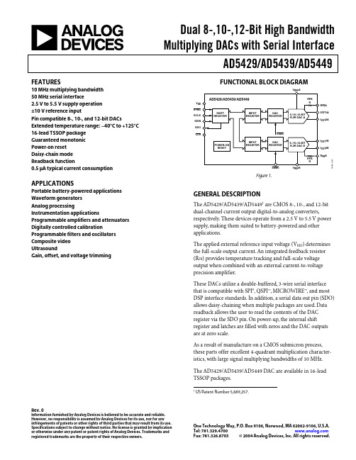
Dual 8-,10-,12-Bit High BandwidthMultiplying DACs with Serial InterfaceAD5429/AD5439/AD5449 Rev.0Information furnished by Analog Devices is believed to be accurate and reliable.However, no responsibility is assumed by Analog Devices for its use, nor for anyinfringements of patents or other rights of third parties that may result from its use. Specifications subject to change without notice. No license is granted by implication or otherwise under any patent or patent rights of Analog Devices. Trademarks and registered trademarks are the property of their respective owners.One Technology Way, P.O. Box 9106, Norwood, MA 02062-9106, U.S.A. Tel: Fax: 781.326.8703© 2004 Analog Devices, Inc. All rights reserved.FEATURES10 MHz multiplying bandwidth50 MHz serial interface2.5 V to 5.5 V supply operation±10 V reference inputPin compatible 8-, 10-, and 12-bit DACs Extended temperature range: −40°C to +125°C 16-lead TSSOP packageGuaranteed monotonicPower-on resetDaisy-chain modeReadback function0.5 µA typical current consumption APPLICATIONSPortable battery-powered applications Waveform generatorsAnalog processingInstrumentation applications Programmable amplifiers and attenuators Digitally controlled calibration Programmable filters and oscillators Composite videoUltrasoundGain, offset, and voltage trimmingFUNCTIONAL BLOCK DIAGRAMSYNCSCLKSDINI OUT1BI OUT1AR FB AI OUT2AI OUT2B4464--1V DDR FB BSDOFigure 1.GENERAL DESCRIPTIONThe AD5429/AD5439/AD54491 are CMOS 8-, 10-, and 12-bit dual-channel current output digital-to-analog converters, respectively. These devices operate from a 2.5 V to 5.5 V power supply, making them suited to battery-powered and other applications.The applied external reference input voltage (V REF) determines the full-scale output current. An integrated feedback resistor (R FB) provides temperature tracking and full-scale voltage output when combined with an external current-to-voltage precision amplifier.These DACs utilize a double-buffered, 3-wire serial interface that is compatible with SPI®, QSPI™, MICROWIRE™, and most DSP interface standards. In addition, a serial data out pin (SDO) allows daisy-chaining when multiple packages are used. Data readback allows the user to read the contents of the DAC register via the SDO pin. On power-up, the internal shift register and latches are filled with zeros and the DAC outputs are at zero scale.As a result of manufacture on a CMOS submicron process, these parts offer excellent 4-quadrant multiplication character-istics, with large signal multiplying bandwidths of 10 MHz. The AD5429/AD5439/AD5449 DAC are available in 16-lead TSSOP packages.1 US Patent Number 5,689,257.AD5429/AD5439/AD5449Rev. 0 | Page 2 of 32TABLE OF CONTENTSSpecifications.....................................................................................3 Timing Characteristics.....................................................................5 Absolute Maximum Ratings............................................................7 ESD Caution..................................................................................7 Pin Configuration and Function Descriptions.............................8 Terminology......................................................................................9 Typical Performance Characteristics...........................................10 General Description.......................................................................15 Unipolar Mode............................................................................15 Bipolar Operation.......................................................................16 Stability........................................................................................16 Single-Supply Applications........................................................17 Positive Output Voltage.............................................................17 Adding Gain................................................................................18 Divider or Programmable Gain Element................................18 Reference Selection....................................................................19 Amplifier Selection....................................................................19 Serial Interface................................................................................20 Microprocessor Interfacing.......................................................22 PCB Layout and Power Supply Decoupling................................24 Power Supplies for the Evaluation Board................................24 Evaluation Board for the DACs................................................24 Overview of AD54xx Devices.......................................................28 Outline Dimensions.......................................................................29 Ordering Guide.. (29)REVISION HISTORY7/04—Revision 0: Initial VersionAD5429/AD5439/AD5449SPECIFICATIONSV DD = 2.5 V to 5.5 V, V REF = 10 V, I OUT2A, I OUT2B = 0 V. All specifications T MIN to T MAX, unless otherwise noted. DC performance measured with OP1177, ac performance with AD9631, unless otherwise noted. Temperature range for Y version is −40°C to +125°C.Table 1.Parameter Min Typ Max Unit ConditionsSTATIC PERFORMANCEAD5429Resolution 8 BitsRelative Accuracy ±0.5 LSBDifferential Nonlinearity ±1 LSB Guaranteed monotonicAD5439Resolution 10 BitsRelative Accuracy ±0.5 LSBDifferential Nonlinearity ±1 LSB Guaranteed monotonicAD5449Resolution 12 BitsRelative Accuracy ±1 LSBDifferential Nonlinearity −1/+2 LSB Guaranteed monotonicGain Error ±10 mVGain Error Temp Coefficient1±5 ppm FSR/°COutput Leakage Current ±5 nA Data = 0000H, T A = 25°C, I OUT1±10 nA Data = 0000H, I OUT1REFERENCE INPUT1Typical resistor TC = −50 ppm/°C Reference Input Range ±10 VV REF A,V REF B Input Resistance 8 10 12 kΩ DAC input resistanceV REF A/B Input Resistance Mismatch 1.6 2.5 % Typ = 25°C, max = 125°CDIGITAL INPUTS/OUTPUT1Input High Voltage, V IH 1.7 V V DD = 2.5 V to 5.5 VInput Low Voltage, V IL0.8 V V DD = 2.7 V to 5.5 V0.7 V V DD = 2.5 V to 2.7 VInput Leakage Current, I IL 1 µAInput Capacitance 10 pFV DD = 4.5 V to 5.5 VOutput Low Voltage, V OL0.4 V I SINK = 200 µAOutput High Voltage, V OH V DD − 1 V I SOURCE = 200 µAV DD = 2.5 V to 3.6 VOutput Low Voltage, V OL0.4 V I SINK = 200 µAOutput High Voltage, V OH V DD − 0.5 V I SOURCE = 200 µADYNAMIC PERFORMANCE1Reference Multiplying BW 10 MHz V REF = 5 V p-p, DAC loaded all 1sOutput Voltage Settling Time Measured to ±4 mV of FS, R LOAD = 100 Ω,C LOAD = 0sAD5429 50 100 nsAD5439 55 110 ns DAC latch alternately loaded with 0sand 1sAD5449 90 160 ns R LOAD = 100 Ω, C LOAD = 15 pFDigital Delay 20 40 nsDigital-to-Analog Glitch Impulse 3 nV-s 1 LSB change around major carry,V REF = 0 VMultiplying Feedthrough Error −75 dB DAC latch loaded with all 0s,reference = 10 kHzRev. 0 | Page 3 of 32AD5429/AD5439/AD5449Rev. 0 | Page 4 of 32ParameterMin Typ Max Unit ConditionsOutput Capacitance 2 pF DAC latches loaded with all 0s4 pF DAC latches loaded with all 1sDigital Feedthrough 5 nV-sFeedthrough to DAC output with CS high and alternate loading of all 0s and all 1s Total Harmonic Distortion −75 dB V REF = 5 V p-p, all 1s loaded, f = 1 kHz−75 dBV REF = 5 V, sine wave generated from digital code Output Noise Spectral Density 25 nV/√Hz@ 1 kHzSFDR PERFORMANCE (Wideband) AD5449, 65 k codes, V REF = 3.5 V Clock = 10 MHz 500 kHz fout 55 dB 100 kHz fout 63 dB 50 kHz fout 65 dB Clock = 25 MHz 500 kHz fout 50 dB 100 kHz fout 60 dB 50 kHz fout 62 dBSFDR PERFORMANCE (Narrow Band) AD5449, 65 k codes, V REF = 3.5 V Clock = 10 MHz 500 kHz fout 73 dB 100 kHz fout 80 dB 50 kHz fout 87 dB Clock = 25 MHz 500 kHz fout 70 dB 100 kHz fout 75 dB 50 kHz fout 80 dBINTERMODULATION DISTORTION AD5449, 65 k codes, V REF = 3.5 V Clock = 10 MHz f 1 = 400 kHz, f 2 = 500 kHz 65 dB f 1 = 40 kHz, f 2 = 50 kHz 72 dB Clock = 25 MHz f 1 = 400 kHz, f 2 = 500 kHz 51 dB f 1 = 40 kHz, f 2 = 50 kHz 65 dB POWER REQUIREMENTS Power Supply Range 2.5 5.5 VI DD 10 µALogic inputs = 0 V or V DD Power Supply Sensitivity 10.001 %/%∆V DD = ±5%1Guaranteed by design and characterization, not subject to production test.AD5429/AD5439/AD5449TIMING CHARACTERISTICSV DD = 2.5 V to 5.5 V, V REF = 5 V, I OUT2 = 0 V. All specifications T MIN to T MAX, unless otherwise noted.See Figure 2 and Figure 3. Temperature range for Y version is −40°C to +125°C. Guaranteed by design and characterization, not subject to production test. All input signals are specified with tr = tf = ns (10% to 90% of V DD) and timed from a voltage level of (V IL + V IH)/2.1 Falling or rising edge as determined by the control bits of the serial word. Strong or weak SDO driver selected via the control register.2 Daisy-chain and readback modes cannot operate at maximum clock frequency. SDO timing specifications are measured with a load circuit, as shown in Figure 4.Rev. 0 | Page 5 of 32AD5429/AD5439/AD5449Rev. 0 | Page 6 of 32SCLKDINLDAC 12NOTES1ASYNCHRONOUS LDAC UPDATE MODE 2ALTERNATIVELY, DATA CAN BE CLOCKED INTO INPUT SHIFT REGISTER ON RISING EDGE OF SCLK AS DETERMINED BY CONTROL BITS. TIMING AS ABOVE, WITH SCLK INVERTED.04464-0-002Figure 2. Standalone Mode Timing Diagram04464-0-003SCLKSYNCSDINSDOALTERNATIVELY, DATA CAN BE CLOCKED INTO INPUT SHIFT REGISTER ON RISING EDGE OF SCLK AS DETERMINED BY CONTROL BITS. IN THIS CASE, DATA WOULD BE CLOCKED OUT OF SDO ON FALLING EDGE OF SCLK. TIMING AS ABOVE, WITH SCLK INVERTED.Figure 3. Daisy-Chain and Readback Modes Timing DiagramPINFigure 4. Load Circuit for SDO Timing SpecificationsAD5429/AD5439/AD5449Rev. 0 | Page 7 of 32ABSOLUTE MAXIMUM RATINGSTable 3.Parameter RatingV DD to GND −0.3 V to +7 VV REF , R FB to GND −12 V to +12 VI OUT 1, I OUT 2 to GND −0.3 V to +7 VInput Current to Any Pin except Supplies ±10 mALogic Inputs and Output 1−0.3 V to V DD + 0.3 VOperating Temperature RangeExtended (Y Version)−40°C to +125°C Storage Temperature Range −65°C to +150°C Junction Temperature150°C 16-Lead TSSOP θJA Thermal Impedance 150°C/W Lead Temperature, Soldering (10 s) 300°C IR Reflow, Peak Temperature (< 20 s)235°C1Overvoltages at SCLK, SYNC , and DIN are clamped by internal diodes. Current should be limited to the maximum ratings given.Stresses above those listed under Absolute Maximum Ratings may cause permanent damage to the device. This is a stress rating only; functional operation of the device at these or any other conditions above those listed in the operational sections of this specification is not implied. Exposure to absolute maximum rating conditions for extended periods may affect device reliability. Only one absolute maximum rating may be applied at any one time. Transient currents of up to 100 mA do not cause SCR latch-up. T A = 25°C unless otherwise noted.ESD CAUTIONESD (electrostatic discharge) sensitive device. Electrostatic charges as high as 4000 V readily accumulate on the human body and test equipment and can discharge without detection. Although this product features proprietary ESD protection circuitry, permanent damage may occur on devices subjected to high energy electrostatic discharges. Therefore, proper ESD precautions are recommended to avoid performancedegradation or loss of functionality.AD5429/AD5439/AD5449Rev. 0 | Page 8 of 32PIN CONFIGURATION AND FUNCTION DESCRIPTIONSNC = NO CONNECT04464-0-005Figure 5. Pin ConfigurationAD5429/AD5439/AD5449Rev. 0 | Page 9 of 32TERMINOLOGYRelative AccuracyRelative accuracy or endpoint nonlinearity is a measure of the maximum deviation from a straight line passing through the endpoints of the DAC transfer function. It is measured after adjusting for zero and full scale and is typically expressed in LSBs or as a percentage of full-scale reading.Differential NonlinearityDifferential nonlinearity is the difference between the measured change and the ideal 1 LSB change between any two adjacent codes. A specified differential nonlinearity of ±1 LSB maximum over the operating temperature range ensures monotonicity. Gain ErrorGain error or full-scale error is a measure of the output error between an ideal DAC and the actual device output. For these DACs, ideal maximum output is V REF − 1 LSB. Gain error of the DACs is adjustable to zero with external resistance.Output Leakage CurrentOutput leakage current is current that flows in the DAC ladder switches when these are turned off. For the I OUT 1 terminal, it can be measured by loading all 0s to the DAC and measuring the I OUT 1 current. Minimum current flows in the I OUT 2 line when the DAC is loaded with all 1s.Output CapacitanceCapacitance from I OUT 1 or I OUT 2 to AGND.Output Current Settling TimeThe amount of time needed for the output to settle to aspecified level for a full-scale input change. For these devices, it is specified with a 100 Ω resistor to ground.Digital-to-Analog Glitch lmpulseThe amount of charge injected from the digital inputs to the analog output when the inputs change state. This is normally specified as the area of the glitch in either pA-s or nV-s,depending upon whether the glitch is measured as a current or voltage signal.Digital FeedthroughWhen the device is not selected, high frequency logic activity on the device digital inputs is capacitively coupled through the device to show up as noise on the I OUT pins and subsequently into the following circuitry. This noise is digital feedthrough. Multiplying Feedthrough ErrorThe error due to capacitive feedthrough from the DAC reference input to the DAC I OUT 1 terminal, when all 0s are loaded to the DAC.Digital CrosstalkThe glitch impulse transferred to the outputs of one DAC in response to a full-scale code change (all 0s to all 1s and vice versa) in the input register of the other DAC. It is expressed in nV-s.Analog CrosstalkThe glitch impulse transferred to the output of one DAC due to a change in the output of another DAC. It is measured byloading one of the input registers with a full-scale code change (all 0s to all 1s and vice versa), while keeping LDAC high. Then pulse LDAC low and monitor the output of the DAC whose digital code was not changed. The area of the glitch is expressed in nV-s.Channel-to-Channel IsolationThe proportion of input signal from the reference input of one DAC that appears at the output of the other DAC. It is expressed in dB.Total Harmonic Distortion (THD)The DAC is driven by an ac reference. The ratio of the rms sum of the harmonics of the DAC output to the fundamental value is the THD. Usually only the lower-order harmonics are included, such as second to fifth.()125242322log20V V V V V THD +++=Intermodulation DistortionThe DAC is driven by two combined sine wave references of frequencies fa and fb. Distortion products are produced at sum and difference frequencies of mfa ± nfb, where m,n = 0, 1, 2, 3… Intermodulation terms are those for which m or n is not equal to zero. The second-order terms include (fa + fb) and (fa − fb) and the third-order terms are (2fa + fb), (2fa − fb), (f + 2fa + 2fb) and (fa − 2fb). IMD is defined as()lfundamenta the of amplitude rms products distortion diff and sum the of sum rms IMD log20=Compliance Voltage RangeThe maximum range of (output) terminal voltage for which the device provides the specified characteristics.AD5429/AD5439/AD5449Rev. 0 | Page 10 of 32TYPICAL PERFORMANCE CHARACTERISTICS–0.20–0.15–0.10–0.0500.05I N L (L S B )0.100.150.2004462-0-007050100150200250CODEFigure 6. INL vs. Code (8-Bit DAC)–0.5–0.4–0.3–0.2–0.100.10.20.30.40.5I N L (L S B )04462-0-0082004006008001000CODEFigure 7. INL vs. Code (10-Bit DAC)–1.0–0.8–0.6–0.4–0.200.20.40.60.81.0I N L (L S B )2000150050010002500300035004000CODE04462-0-009Figure 8. INL vs. Code (12-Bit DAC) –0.20–0.15–0.10–0.0500.05D N L (L S B )0.100.150.2004462-0-010050100150200250CODEFigure 9. DNL vs. Code (8-Bit DAC)–0.5–0.4–0.3–0.2–0.100.10.20.30.40.5D N L (L S B )04462-0-01102004006008001000CODEFigure 10. DNL vs. Code (10-Bit DAC)–1.0–0.8–0.6–0.4–0.200.20.40.60.81.0D N L (L S B )2000150050010002500300035004000CODE04462-0-012Figure 11. DNL vs. Code (12-Bit DAC)–0.3–0.2–0.100.10.20.30.40.50.6I N L (L S B )65342789REFERENCE VOLTAGE04462-0-01310Figure 12. INL vs. Reference Voltage–0.70–0.65–0.60–0.55–0.50–0.45–0.40D N L (L S B )65342789REFERENCE VOLTAGE04462-0-01410Figure 13. DNL vs. Reference Voltage–5–4–3–2–1012345E R R O R (m V )–60–40–20020406080100120140TEMPERATURE (°C)04462-0-015Figure 14. Gain Error vs. TemperatureINPUT VOLTAGE (V)C U R R E N T (m A )850 5.0763142 4.54.03.53.02.52.01.51.00.504462-0-022Figure 15. Supply Current vs. Logic Input Voltage00.20.40.60.81.0I O U T L E A K A G E (n A )1.21.41.6TEMPERATURE (°C)04462-0-023Figure 16. I OUT 1 Leakage Current vs. Temperature00.050.100.150.200.250.300.350.400.450.50C U R R E N T (µA )–60–40–20020406080100120140TEMPERATURE (°C)04462-0-024Figure 17. Supply Current vs. Temperature2468101214I D D (m A )10k 1k 101001100k 1M 10M 100MFREQUENCY (Hz)04462-0-025Figure 18. Supply Current vs. Update Rate–102–66–54–42–30–18–6611001k 10k 100k 1M10M100MFREQUENCY (Hz)G A I N (d B )0–60–48–36–24–12–84–72–78–90–9604462-0-02610Figure 19. Reference Multiplying Bandwidth vs. Frequency and Code–0.8–0.6–0.4–0.20.2G A I N (d B )10k 1k 101001100k 1M 10M 100M FREQUENCY (Hz)04462-0-027Figure 20. Reference Multiplying Bandwidth–All 1s Loaded–9–6–3310k100k1M10M100MFREQUENCY (Hz)G A I N (d B )04462-0-028Figure 21. Reference Multiplying Bandwidth vs. Frequency andCompensation Capacitor–0.010–0.0050.0050.0250.0350.0450.01500.0200.0300.0400.010O U T P U T V O L T A G E (V )20406080100120140160180200TIME (ns)04462-0-041Figure 22. Midscale Transition, V REF = 0 VO U T P U T V O L T A G E (V )020406080100120140160180200TIME (ns)04462-0-042–1.77–1.76–1.75–1.74–1.73–1.72–1.71–1.70–1.69–1.68Figure 23. Midscale Transition, V REF = 3.5 V–120–100–80–60020FREQUENCY (Hz)–40–20P S R R (d B )04462-0-04310Figure 24. Power Supply Rejection vs. Frequency–90–85–80–75–70–65–60T H D + N (d B )1001k11010k100k1MFREQUENCY (Hz)04462-0-044Figure 25. THD + Noise vs. Frequency20406080100S F D R (d B )020406080100120140160180200f OUT (kHz)04462-0-045Figure 26. Wideband SFDR vs. f OUT Frequency102030405060708090S F D R (d B )1002003004005006007008009001000f OUT (kHz)04462-0-046Figure 27. Wideband SFDR vs. f OUT Frequency04462-0-047–90–70–50–30–10S F D R (d B )FREQUENCY (MHz)–80–60–40–20024681012Figure 28. Wideband SFDR, f OUT = 100 kHz, Clock = 25 MHz044620-048–100–70–50–30–10S F D R (d B )FREQUENCY (MHz)–80–60–40–2000.51.53.0 3.54.01.02.0 2.5 4.55.0–90Figure 29. Wideband SFDR, f OUT = 500 kHz, Clock = 10 MHz04462-0-049–90–70–50–30–10S F D R (d B )0FREQUENCY (MHz)–80–60–40–2000.5 1.53.0 3.54.01.0 2.0 2.5 4.55.0Figure 30. Wideband SFDR, f OUT = 50 kHz, Clock = 10 MHz04462-0-050FREQUENCY (MHz)–100–70–50–30–10S F D R (d B )250750300350400650700–80–60–40–200–90450500550600Figure 31. Narrow-Band Spectral Response, f OUT = 500 kHz, Clock = 25 MHz04462-0-051–120–60–20S F D R (d B )50150FREQUENCY (MHz)607080130140–80–40020–10090100110120Figure 32. Narrow-Band SFDR, f OUT = 100 kHz, Clock = 25 MHz04462-0-052FREQUENCY (MHz)–100–70–50–30–10(d B )70120758085115–80–60–40–200–909010010511095Figure 33. Narrow-Band IMD, f OUT = 90 kHz, 100 kHz, Clock = 10 MHz04462-0-053–100–40–20(d B )–50–30–10–90–60–70–800400FREQUENCY (kHz)503003501001502002500Figure 34. Wideband IMD, f OUT = 90 kHz, 100 kHz, Clock = 25 MHzFREQUENCY (Hz)04462-0-054050100150200250300O U T P U T N O I S E (n V H z )Figure 35. Output Noise Spectral DensityGENERAL DESCRIPTIONThe AD5429/AD5439/AD5449 are 8-, 10-, and 12-bit dual-channel current output DACs consisting of a standard inverting R−2R ladder configuration. A simplified diagram of one DAC channel for the AD5449 is shown in Figure 36. The feedback resistor R FB has a value of R. The value of R is typically 10 kΩ (minimum 8 kΩ and maximum 12 kΩ). If I OUT 1 and I OUT 2 are kept at the same potential, a constant current flows in each ladder leg, regardless of digital input code. Therefore, the input resistance presented at V REF is always constant.R FB A I OUT 1A I OUT 2AV REF A04464-0-006Figure 36. Simplified LadderAccess is provided to the V REF , R FB , I OUT 1, and I OUT 2 terminals of the DACs, making the devices extremely versatile and allowing them to be configured in several operating modes, such as unipolar mode, bipolar output mode, or single-supply mode.UNIPOLAR MODEUsing a single op amp, these devices can easily be configured to provide 2-quadrant multiplying operation or a unipolar output voltage swing, as shown in Figure 37.When an output amplifier is connected in unipolar mode, the output voltage is given byn REF OUT D V V 2/×−=where D is the fractional representation of the digital word loaded to the DAC, and n is the number of bits. D = 0 to 255 (AD5429) = 0 to 1023 (AD5439) = 0 to 4095 (AD5449)With a fixed 10 V reference, the circuit shown in Figure 37 gives a unipolar 0 V to −10 V output voltage swing. When V IN is an ac signal, the circuit performs 2-quadrant multiplication.Table 5 shows the relationship between digital code and the expected output voltage for unipolar operation for the AD5429.Table 5. Unipolar Code TableDigital Input Analog Output (V) 1111 1111 −V REF (4095/4096)1000 0000 −V REF (2048/4096) = −V REF /2 0000 0001 −V REF (1/4096) 0000 0000−V REF (0/4096) = 004464-0-007NOTES:1. R1 AND R2 USED ONLY IF GAIN ADJUSTMENT IS REQUIRED.2. C1 PHASE COMPENSATION (1pF TO 2pF) MAY BE REQUIRED3. DAC B OMITTED FOR CLARITY.V –V REFV IF A1 IS A HIGH SPEED AMPLIFIER.Figure 37. Unipolar OperationBIPOLAR OPERATIONIn some applications, it might be necessary to generate full 4-quadrant multiplying operation or a bipolar output swing. This can be easily accomplished by using another external amplifier and three external resistors, as shown in Figure 38. When V IN is an ac signal, the circuit performs 4-quadrant multiplication. When connected in bipolar mode, the output voltage is()REF n REF OUT V D V V −×=−12/where D is the fractional representation of the digital word loaded to the DAC, and n is the number of bits. D = 0 to 255 (AD5429) = 0 to 1023 (AD5439) = 0 to 4095 (AD5449)Table 6 shows the relationship between digital code and the expected output voltage for bipolar operation with the AD5429. Table 6. Bipolar Code TableDigital Input Analog Output (V) 1111 1111 +V REF (2047/2048) 1000 0000 00000 0001 −V REF (2047/2048) 0000 0000−V REF (2048/2048)STABILITYIn the I-to-V configuration, the I OUT of the DAC and theinverting node of the op amp must be connected as closely as possible, and proper PCB layout techniques must be employed. Because every code change corresponds to a step function, gain peaking can occur, if the op amp has limited GBP and there is excessive parasitic capacitance at the inverting node. This parasitic capacitance introduces a pole into the open loop response, which can cause ringing or instability in the closed-loop applications circuit.As shown in Figure 37 and Figure 38, an optional compensation capacitor, C1, can be added in parallel with R FB for stability. Too small a value of C1 can produce ringing at the output, while too large a value can adversely affect the settling time. C1 should be found empirically, but 1 pF to 2 pF is generally adequate for the compensation.04464-0-008REF TO +V REFV REF 1. R1 AND R2 USED ONLY IF GAIN ADJUSTMENT IS REQUIRED.2. MATCHING AND TRACKING IS ESSENTIAL FOR RESISTOR PAIRS3. C1 PHASE COMPENSATION (1pF TO 2pF) MAY BE REQUIRED,4. DAC B AND ADDITIONAL PINS OMITTED FOR CLARITY.IF A1/A2 IS A HIGH SPEED AMPLIFIER.ADJUST R1 FOR V OUT = 0V WITH CODE 10000000 LOADED TO DAC.R3 AND R4.R3Figure 38. Bipolar OperationSINGLE-SUPPLY APPLICATIONSVoltage-Switching ModeFigure 39 shows the DACs operating in voltage-switching mode. The reference voltage, V IN , is applied to the I OUT 1 pin, I OUT 2 is connected to AGND, and the output voltage is available at the V REF terminal. In this configuration, a positive reference voltage results in a positive output voltage, making single-supply operation possible. The output from the DAC is voltage at a constant impedance (the DAC ladder resistance). Therefore, an op amp is necessary to buffer the output voltage. The reference input no longer sees a constant input impedance, but one that varies with code. So, the voltage input should be driven from a low impedance source.Note that V IN is limited to low voltages, because the switches in the DAC ladder no longer have the same source-drain drive voltage. As a result, their on resistance differs and this degrades the integral linearity of the DAC. Also, V IN must not go negative by more than 0.3 V or an internal diode turns on, exceeding the maximum ratings of the device. In this type of application, the DAC’s full range of multiplying capability is lost.POSITIVE OUTPUT VOLTAGEThe output voltage polarity is opposite to the V REF polarity for dc reference voltages. To achieve a positive voltage output, an applied negative reference to the input of the DAC is preferred over the output inversion through an inverting amplifierbecause of the resistor’s tolerance errors. To generate a negative reference, the reference can be level-shifted by an op amp such that the V OUT and GND pins of the reference become the virtual ground and −2.5 V , respectively, as shown in Figure 40.OUTV V 04464-0-009NOTES:1. ADDITIONAL PINS OMITTED FOR CLARITY.2. C1 PHASE COMPENSATION (1pF–2pF) MAY BE REQUIRED IF A1 IS A HIGH SPEED AMPLIFIER.Figure 39. Single-Supply Voltage-Switching ModeV = +5V04464-0-0101. ADDITIONAL PINS OMITTED FOR CLARITY.2. C1 PHASE COMPENSATION (1pF–2pF) MAY BE REQUIRED IF A1 IS A HIGH SPEED AMPLIFIER.Figure 40. Positive Voltage Output with Minimum Components。
运算放大器(AD549)应用中文技术资料

极低偏置电流运算放大器AD5491 概述AD549是具有极低输入偏置电流的单片电路静电计型运算放大器。
为达到高精度的目的,输入偏置电压和输入偏置电压漂移均通过激光调节。
这种极低输入电流性能由ADI公司专有的topgate工艺技术完成。
该技术可以制造与具有极低输入电流的JFET并与双极性电路隔离的集成运放。
输入级具有1015Ω的共模阻抗,其输入电流与共模电压无关。
AD549适用于低输入电流和低输入偏置电压的场合。
它特别适合用作各种电流输出的传感器,如光电二极管、光电倍增管以及氧气传感器等的前置放大器。
该产品也可用作精密积分器或低衰减采样保持器。
AD549的封装与标准FET和静电计运算放大器兼容,因此用户花少量成本即可对系统升级,提高已有系统的性能。
AD549有TO-99密封封装。
金属外壳与8管脚相连,使得金属外壳与同样电压的输入终端独立连接,达到降低外壳泄漏的目的。
AD549具有四种性能等级。
其中J、K和L型号的温度范围是0℃到70℃。
S型号专用于军事,其温度范围:-55℃到125℃。
AD549的输入电流在整个共模输入电压范围内都得到保证,其输入失调电压和漂移由激光分别调节到0.25mV和5μV/℃(AD549K);1mV和20μV/℃(AD549J)。
700μA的最大静态电流使输入电流和偏置电压的热效应降到最低。
模拟性能包括1MHz的均匀增益带宽和3V/μs的压摆率。
当输入为10V时,建立时间是5μs 到0.01%。
2 AD549的引脚及特性参数图一所示是AD549的引脚图,表一所示是其特性参数。
图一AD549引脚图表一AD549的主要特性nV/ nV/ nV/ nV/3 AD549的工作原理3.1 最小化输入电流AD549具有很小的输入电流和失调电压。
在实际应用中应谨慎考虑如何使用放大器可以减小输入电流。
为减小输入电流,该放大器的工作温度应尽可能低。
像其他JFET输入放大器一样,AD549的输入电流对芯片温度很敏感,上升斜率因子为每10℃的2.3。
AD549_08资料
FEATURES
Ultralow input bias current 60 fA maximum (AD549L) 250 fA maximum (AD549J)
Input bias current guaranteed over the common-mode voltage range
Ultralow Input Bias Current Operational Amplifier AD549
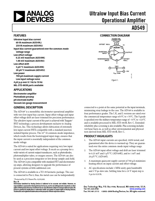
CONNECTION DIAGRAM
GUARD PIN, CONNECTED
TO CASE
OFFSET NULL
8
V+
1 AD549 7
INVERTING INPUT
2
6 OUTPUT
3 NONINVERTING
4. AC specifications include 1 MHz unity-gain bandwidth and 3 V/μs slew rate. Settling time for a 10 V input step is 5 μs to 0.01%.
One Technology Way, P.O. Box 9106, Norwood, MA 02062-9106, U.S.A.
Tel: 781.329.4700
Fax: 781.461.3113 ©2002–2008 Analog Devices, Inc. All rights reserved.
元器件交易网
AD549
TABLE OF CONTENTS
Features .............................................................................................. 1 Applications....................................................................................... 1 Connection Diagram ....................................................................... 1 General Description ......................................................................... 1 Product Highlights ........................................................................... 1 Revision History ............................................................................... 2 Specifications..................................................................................... 3 Absolute Maximum Ratings............................................................ 5
tlc549数字系统课程设计
tlc549数字系统课程设计一、课程目标知识目标:1. 学生能够理解tlc549数字系统的基础知识,掌握其工作原理和功能特点。
2. 学生能够运用数字系统相关知识,分析并设计简单的tlc549应用电路。
3. 学生了解数字系统的基本组成部分,掌握数字信号处理的基本概念。
技能目标:1. 学生能够运用所学知识,使用相关软件或工具进行tlc549数字系统的设计和仿真。
2. 学生具备实际操作能力,能够搭建并调试简单的tlc549应用电路。
3. 学生能够独立解决数字系统设计中遇到的问题,具备一定的故障排查和优化能力。
情感态度价值观目标:1. 学生对数字系统产生兴趣,提高学习积极性,培养良好的学习习惯。
2. 学生通过课程学习,认识到数字技术在现实生活中的重要性,增强对科技创新的热情。
3. 学生在团队合作中,学会尊重他人意见,培养沟通协作能力和解决问题的能力。
课程性质:本课程为实践性较强的数字系统设计课程,结合理论知识与实际操作,培养学生的实际应用能力。
学生特点:学生已具备一定的电子基础和数字电路知识,具有较强的学习能力和动手能力。
教学要求:课程要求学生掌握tlc549数字系统的基础知识,能够运用所学知识进行实际设计和操作,注重培养学生的实践能力和创新精神。
通过课程目标的分解,使学生在知识、技能和情感态度价值观方面取得具体的学习成果,为后续教学设计和评估提供明确方向。
二、教学内容1. 数字系统基础知识回顾:数字信号与模拟信号的区别,数字系统的基本组成部分,数字电路的基本原理。
教材章节:第一章 数字系统概述2. tlc549芯片原理与功能:介绍tlc549芯片的工作原理,性能参数,应用领域。
教材章节:第三章 数字电路器件3. tlc549应用电路设计:分析并设计简单的tlc549应用电路,如模数转换电路、信号采集电路等。
教材章节:第四章 数字电路设计与实践4. 数字系统设计与仿真:运用相关软件或工具,如Multisim、Proteus等,进行tlc549数字系统的设计与仿真。
ADS5493EVM;中文规格书,Datasheet资料

User's GuideSLAU325–September2010ADS5493EVM Evaluation Module This evaluation module(EVM)user's guide gives an overview of the ADS5493EVM and provides a general description of the features and functions to be considered while using this module.Contents1Evaluation Module Description (2)2Software Installation (3)3ADS5493EVM Software–SPI Control (4)4Initial EVM Setup and Basic Test Procedure (5)5Power Supply Options (6)List of Figures1ADS5493EVM Overview (2)2Installation Process of ADS5493EVM Software (3)3EVM Software Front Panel (4)4EVM Software Advanced Tab (4)5Basic EVM Hardware Setup (5)6Schematic Modification of the Analog Input Path (5)7Typical Performance Screenshot (6)8Power Supply Options on the ADS5493EVM (6)1 SLAU325–September2010ADS5493EVM Evaluation Module Submit Documentation FeedbackGND Analog InputSignal Clock InputPower SupplyJumper OptionsEvaluation Module Description 1Evaluation Module DescriptionThe ADS5493evaluation module (EVM)is easy to set up and provides the user flexibility.On the analog side,the user can evaluate different transformers and configurations while the EVM also allows asingle-ended or differential clock input.The EVM is powered from a single 5-V power input;the user can select either LDO or switching regulator option for generating the analog and digital 3.3-V supplies for the ADS5493.On the digital side,the EVM provides a seamless interface to the TSW1200capture card in order toevaluate received data directly on a personal computer (PC).The internal registers of the ADS5493can be conveniently accessed and programmed via SPI through the USB connection using the GUI or the TSW1200.The ADS5493EVM works well in default configuration;no register programming is required.Figure 1.ADS5493EVM Overview2ADS5493EVM Evaluation ModuleSLAU325–September 2010Submit Documentation Feedback Software Installation 2Software Installation1.Open the folder named ADS5493_Installer_vxpx (xpx represents the latest version).2.Run Setup.exe.3.Follow the on-screen instructions.4.Once installed,launch by clicking on the ADS5493_GUI_vxpx program in Start >Texas InstrumentsADCs.5.When plugging in the USB cable for the first time,you are prompted to install the USB drivers for USBSerial Converter and USB Serial Port (see Figure 2).(a)Follow the on-screen instructions to install the USB drivers.(b)If needed,you can access the drivers directly in the install directoryFigure 2.Installation Process of ADS5493EVM Software2.1ADS5493.ini file for TSW1200The ADS5493software package comes with a new ini file for the TSW1200.Manually place thisADS5493.ini file into the following directory in order for the TSW1200to recognize it:C:\Program Files\Texas Instruments\TSW1200\ADC Files3SLAU325–September 2010ADS5493EVM Evaluation ModuleSubmit Documentation FeedbackTabs to control allregisters as well asindividual registerwrites on‘advanced’pageIndividual controlregistersControl to send or read all registersas well as load or save register files Reset USB port on FTDIchip –required after powerup of ADS5493EVM Warning indication that USBcommunication is not established Summary of current registers being writtenshowing address and data in hex format‘Advanced’TabOption to write toindividual registers directlyADS5493EVM Software –SPI Control 3ADS5493EVM Software –SPI ControlThe ADS5493is fully functional without the need for register writes;however,the EVM software provides register access to the user.The ADS5493EVM software controls the ADS5493via SPI register writes through a USB connection with the PC.Figure 3is a snapshot of the GUI front panel,highlighting the two tabs to control the setup ofADS5493.It is necessary to perform a USB reset after applying power to the EVM to establish proper connection with the PC.Otherwise,a warning sign on the bottom right flashes,indicating a USB communicationfailure.The EVM software also provides the option to save all registers to a file or to load registers from a file.The display in the bottom right corner provides a summary of all the registers being currently written.Figure 3.EVM Software Front PanelThe Advanced tab allows the user to access the SPI registers directly using individual register writes.Figure 4.EVM Software Advanced Tab4ADS5493EVM Evaluation ModuleSLAU325–September 2010Submit Documentation FeedbackAinClock Initial EVM Setup and Basic Test Procedure 4Initial EVM Setup and Basic Test ProcedureThe fastest way to get the ADS5493EVM up and running is to follow this operating procedure:1.Two signal generators must be connected to the clock and data input of the EVM –preferably withband-pass filter and the 10-MHz reference locked for coherency2.The TSW1200capture card must be plugged in ADS5493EVM and connected to the PC via USB.3.All appropriate power supplies must be connected.4.After performing a USB reset in the ADS5493EVM software,the flashing USB warning signdisappears,indicating successful USB communication.Figure 5.Basic EVM Hardware SetupThe analog input path has a 8.2-pF differential input capacitor at the analog inputs of the ADC as shown in the EVM schematic.This capacitor helps to boost the SFDR performance at higher input frequencies (>50MHz)but is less effective at lower input frequencies.Figure 6.Schematic Modification of the Analog Input PathIn the TSW1200,the ADC selection must be set to ADS5493.Figure 7shows a typical performance plot at 100-MHz IF with a sample rate of 130Msps.In this specific setup,SNR is expected to be in the range of 74–76dBFS whereas SFDR is expected to be better than 91dBc.5SLAU325–September 2010ADS5493EVM Evaluation ModuleSubmit Documentation FeedbackPower Supply Options Figure 7.Typical Performance Screenshot5Power Supply OptionsThe ADS5493EVM is designed to operate from an external 5-V supply,which also connects to the 5-V analog supply of the ADS5493.The user has the option to generate the 3.3V for the analog and digital supplies of the ADS5493either with a LDO (TPS79533)or a switching regulator (TPS62237)by setting jumper JP2and JP3accordingly.The EVM also provides additional pin headers so that the individual voltages for 5V VDDA,3.3V VDDA and 3.3V DVDD can be supplied directly,e.g.,for accurate power consumption measurements.6ADS5493EVM Evaluation ModuleSLAU325–September 2010Submit Documentation FeedbackEvaluation Board/Kit Important NoticeTexas Instruments(TI)provides the enclosed product(s)under the following conditions:This evaluation board/kit is intended for use for ENGINEERING DEVELOPMENT,DEMONSTRATION,OR EVALUATION PURPOSES ONLY and is not considered by TI to be a finished end-product fit for general consumer use.Persons handling the product(s)must have electronics training and observe good engineering practice standards.As such,the goods being provided are not intended to be complete in terms of required design-,marketing-,and/or manufacturing-related protective considerations, including product safety and environmental measures typically found in end products that incorporate such semiconductor components or circuit boards.This evaluation board/kit does not fall within the scope of the European Union directives regarding electromagnetic compatibility,restricted substances(RoHS),recycling(WEEE),FCC,CE or UL,and therefore may not meet the technical requirements of these directives or other related directives.Should this evaluation board/kit not meet the specifications indicated in the User’s Guide,the board/kit may be returned within30 days from the date of delivery for a full refund.THE FOREGOING WARRANTY IS THE EXCLUSIVE WARRANTY MADE BY SELLER TO BUYER AND IS IN LIEU OF ALL OTHER WARRANTIES,EXPRESSED,IMPLIED,OR STATUTORY,INCLUDING ANY WARRANTY OF MERCHANTABILITY OR FITNESS FOR ANY PARTICULAR PURPOSE.The user assumes all responsibility and liability for proper and safe handling of the goods.Further,the user indemnifies TI from all claims arising from the handling or use of the goods.Due to the open construction of the product,it is the user’s responsibility to take any and all appropriate precautions with regard to electrostatic discharge.EXCEPT TO THE EXTENT OF THE INDEMNITY SET FORTH ABOVE,NEITHER PARTY SHALL BE LIABLE TO THE OTHER FOR ANY INDIRECT,SPECIAL,INCIDENTAL,OR CONSEQUENTIAL DAMAGES.TI currently deals with a variety of customers for products,and therefore our arrangement with the user is not exclusive.TI assumes no liability for applications assistance,customer product design,software performance,or infringement of patents or services described herein.Please read the User’s Guide and,specifically,the Warnings and Restrictions notice in the User’s Guide prior to handling the product.This notice contains important safety information about temperatures and voltages.For additional information on TI’s environmental and/or safety programs,please contact the TI application engineer or visit /esh.No license is granted under any patent right or other intellectual property right of TI covering or relating to any machine,process,or combination in which such TI products or services might be or are used.FCC WarningThis evaluation board/kit is intended for use for ENGINEERING DEVELOPMENT,DEMONSTRATION,OR EVALUATION PURPOSES ONLY and is not considered by TI to be a finished end-product fit for general consumer use.It generates,uses,and can radiate radio frequency energy and has not been tested for compliance with the limits of computing devices pursuant to part15 of FCC rules,which are designed to provide reasonable protection against radio frequency interference.Operation of this equipment in other environments may cause interference with radio communications,in which case the user at his own expense will be required to take whatever measures may be required to correct this interference.EVM Warnings and RestrictionsIt is important to operate this EVM within the input voltage range of-0.3V to5.3V and the output voltage range of-0.3V to3.6V. Exceeding the specified input range may cause unexpected operation and/or irreversible damage to the EVM.If there are questions concerning the input range,please contact a TI field representative prior to connecting the input power.Applying loads outside of the specified output range may result in unintended operation and/or possible permanent damage to the EVM.Please consult the EVM User's Guide prior to connecting any load to the EVM output.If there is uncertainty as to the load specification,please contact a TI field representative.During normal operation,some circuit components may have case temperatures greater than50°C.The EVM is designed to operate properly with certain components above25°C as long as the input and output ranges are maintained.These components include but are not limited to linear regulators,switching transistors,pass transistors,and current sense resistors.These types of devices can be identified using the EVM schematic located in the EVM User's Guide.When placing measurement probes near these devices during operation,please be aware that these devices may be very warm to the touch.Mailing Address:Texas Instruments,Post Office Box655303,Dallas,Texas75265Copyright©2010,Texas Instruments IncorporatedIMPORTANT NOTICETexas Instruments Incorporated and its subsidiaries(TI)reserve the right to make corrections,modifications,enhancements,improvements, and other changes to its products and services at any time and to discontinue any product or service without notice.Customers should obtain the latest relevant information before placing orders and should verify that such information is current and complete.All products are sold subject to TI’s terms and conditions of sale supplied at the time of order acknowledgment.TI warrants performance of its hardware products to the specifications applicable at the time of sale in accordance with TI’s standard warranty.Testing and other quality control techniques are used to the extent TI deems necessary to support this warranty.Except where mandated by government requirements,testing of all parameters of each product is not necessarily performed.TI assumes no liability for applications assistance or customer product design.Customers are responsible for their products and applications using TI components.To minimize the risks associated with customer products and applications,customers should provide adequate design and operating safeguards.TI does not warrant or represent that any license,either express or implied,is granted under any TI patent right,copyright,mask work right, or other TI intellectual property right relating to any combination,machine,or process in which TI products or services are rmation published by TI regarding third-party products or services does not constitute a license from TI to use such products or services or a warranty or endorsement e of such information may require a license from a third party under the patents or other intellectual property of the third party,or a license from TI under the patents or other intellectual property of TI.Reproduction of TI information in TI data books or data sheets is permissible only if reproduction is without alteration and is accompanied by all associated warranties,conditions,limitations,and notices.Reproduction of this information with alteration is an unfair and deceptive business practice.TI is not responsible or liable for such altered rmation of third parties may be subject to additional restrictions.Resale of TI products or services with statements different from or beyond the parameters stated by TI for that product or service voids all express and any implied warranties for the associated TI product or service and is an unfair and deceptive business practice.TI is not responsible or liable for any such statements.TI products are not authorized for use in safety-critical applications(such as life support)where a failure of the TI product would reasonably be expected to cause severe personal injury or death,unless officers of the parties have executed an agreement specifically governing such use.Buyers represent that they have all necessary expertise in the safety and regulatory ramifications of their applications,and acknowledge and agree that they are solely responsible for all legal,regulatory and safety-related requirements concerning their products and any use of TI products in such safety-critical applications,notwithstanding any applications-related information or support that may be provided by TI.Further,Buyers must fully indemnify TI and its representatives against any damages arising out of the use of TI products in such safety-critical applications.TI products are neither designed nor intended for use in military/aerospace applications or environments unless the TI products are specifically designated by TI as military-grade or"enhanced plastic."Only products designated by TI as military-grade meet military specifications.Buyers acknowledge and agree that any such use of TI products which TI has not designated as military-grade is solely at the Buyer's risk,and that they are solely responsible for compliance with all legal and regulatory requirements in connection with such use. TI products are neither designed nor intended for use in automotive applications or environments unless the specific TI products are designated by TI as compliant with ISO/TS16949requirements.Buyers acknowledge and agree that,if they use any non-designated products in automotive applications,TI will not be responsible for any failure to meet such requirements.Following are URLs where you can obtain information on other Texas Instruments products and application solutions:Products ApplicationsAmplifiers Audio /audioData Converters Automotive /automotiveDLP®Products Communications and /communicationsTelecomDSP Computers and /computersPeripheralsClocks and Timers /clocks Consumer Electronics /consumer-appsInterface Energy /energyLogic Industrial /industrialPower Mgmt Medical /medicalMicrocontrollers Security /securityRFID Space,Avionics&/space-avionics-defenseDefenseRF/IF and ZigBee®Solutions /lprf Video and Imaging /videoWireless /wireless-appsMailing Address:Texas Instruments,Post Office Box655303,Dallas,Texas75265Copyright©2010,Texas Instruments Incorporated分销商库存信息: TIADS5493EVM。
串行AD转换器TLC549的应用设计

课程设计任务书题目串行AD转换器TLC549的应用设计系(部) 信息科学与电气工程学院专业电子信息工程班级电信091班学生姓名王凤娟学号09081924512 月26 日至12 月30 日共 1 周指导教师(签字)系主任(签字)2011年12 月30 日摘要本次课程设计的主要目的,就是通过应用8位串行模数转换器TLC549采集电压信号,并进行AD转换,转换成数字信号传送给51单片机,在单片机内部通过编写程序进行数据处理,最后通过单片机的I/O口控制芯片74LS164显示出所采集的电压大小,另外利用键盘控制电压大小的上下限,也即量程,如果超出上下限,则指示灯发光。
关键字:TLC549 AD转换74LS164 量程AbstractIn this class, the design of the main purpose, is through the application of eight serial adc voltage signal collection of eight bits, and AD transform, converted into digital signals to 51 single-chip microcomputer, the microcontroller internal by writing program data processing, the last through the single-chip microcomputer of I/O mouth control chip 74 LS164 shows which collection of voltage size, in addition to use the keyboard control voltage size the upper and lower limits that range, if exceeded the upper and lower limits of the indicator light to shine.Key words:TLC549eight bits AD transform 74 LS164 range目录摘要............................................................................................................... 错误!未定义书签。
AD549JHZ资料

1. The AD549 input currents are specified, 100% tested, and guaranteed after the device is warmed up. They are guaranteed over the entire common-mode input voltage range.
Ultralow Input Bias Current Operational Amplifier AD549
CONNECTION DIAGRAM
GUARD PIN, CONNECTED
TO CASE
SET NULL
8
V+
1 AD549 7
INVERTING INPUT
2
6 OUTPUT
3 NONINVERTING
2. The AD549 input offset voltage and drift are laser trimmed to 0.25 mV and 5 μV/°C (AD549K), and to 1 mV and 20 μV/°C (AD549J).
3. A maximum quiescent supply current of 700 μA minimizes heating effects on input current and offset voltage.
ESD Caution.................................................................................. 5 Typical Performance Characteristics ............................................. 6 Functional Description .................................................................. 10
Latitude 5490 用户手册.pdf_1700373621.7257783说明书

Latitude 5490用户手册8 2021注意、小心和警告:“注意”表示帮助您更好地使用该产品的重要信息。
:“小心”表示可能会损坏硬件或导致数据丢失,并告诉您如何避免此类问题。
:“警告”表示可能会导致财产损失、人身伤害甚至死亡。
© 2019-2021 Dell Inc. 或其子公司。
保留所有权利。
Dell、EMC 和其他商标是 Dell Inc. 或其附属机构的商标。
其他商标可能是其各自所有者的商标。
章 1: 拆装计算机内部组件 (7)安全防范措施 (7)静电放电— ESD 保护 (7)ESD 现场服务套件 (8)运输敏感组件 (8)拆装计算机内部组件之前 (8)拆装计算机内部组件之后 (9)章 2: 卸下和安装组件 (10)建议工具 (10)螺钉大小列表 (10)用户识别模块 (SIM) 板 (11)卸下用户识别模块卡 (11)安装用户识别模块卡 (12)基座盖 (12)卸下基座护盖 (12)安装基座护盖 (14)电池 (14)锂离子电池预防措施 (14)卸下电池 (14)安装电池 (15)固态驱动器—可选 (15)卸下 SSD 卡 (15)安装 SSD 卡 (16)卸下 SSD 框架 (16)安装 SSD 框架 (17)硬盘驱动器 (17)卸下硬盘驱动器 (17)安装硬盘驱动器 (18)币形电池 (19)卸下币形电池 (19)安装币形电池 (19)WLAN 卡 (20)卸下 WLAN 卡 (20)安装 WLAN 卡 (22)WWAN 卡–可选 (22)卸下 WWAN 卡 (22)安装 WWAN 卡 (23)内存模块 (23)卸下内存模块 (23)安装内存模块 (24)键盘格架和键盘 (24)卸下键盘格架 (24)安装键盘格架 (24)目录3卸下键盘 (25)安装键盘 (27)散热器 (27)卸下散热器 (27)安装散热器 (28)系统风扇 (28)卸下系统风扇 (28)安装系统风扇 (29)电源连接器端口 (30)卸下电源连接器端口 (30)安装电源连接器端口 (30)机箱框架 (31)卸下机箱框架 (31)安装机箱框架 (32)智能卡模块 (32)卸下智能卡读取器板 (32)安装智能卡读取器板 (34)扬声器 (34)卸下扬声器 (34)安装扬声器 (35)系统板 (36)卸下系统板 (36)安装系统板 (39)显示屏铰接部件护盖 (40)卸下显示屏铰接部件护盖 (40)安装显示屏铰接部件护盖 (40)显示屏部件 (41)卸下显示屏部件 (41)安装显示屏部件 (44)显示屏挡板 (44)卸下显示屏挡板 (44)安装显示屏挡板 (45)显示屏面板 (45)卸下显示屏面板 (45)安装显示屏面板 (47)显示屏 (eDP) 电缆 (47)卸下显示屏电缆 (47)安装显示屏电缆 (48)摄像头 (49)卸下摄像头 (49)安装摄像头 (49)显示屏铰接部件 (50)卸下显示屏铰接部件 (50)安装显示屏铰接部件 (51)显示屏后盖部件 (51)卸下显示屏后盖部件 (51)安装显示屏后盖部件 (52)掌垫 (52)卸下掌垫 (52)安装掌垫 (53)4目录章 3: 技术规格 (55)处理器 (55)内存 (55)存储规格 (56)音频规格 (56)视频规格 (57)摄像头选项 (57)端口和接口 (57)接触式智能卡规格 (58)显示屏技术规范 (58)键盘规格 (59)触摸板规格 (60)电池规格 (61)交流适配器规格 (61)系统尺寸 (62)操作条件 (62)章 4: 技术和组件 (63)电源适配器 (63)Kaby Lake —第 7 代 Intel Core 处理器 (63)Kaby Lake 更新—第 8 代 Intel Core 处理器 (64)DDR4 (65)HDMI 1.4 (66)HDMI 1.4 (66)USB 功能 (67)DisplayPort(带有 USB Type-C)的优势 (68)USB Type-C (69)章 5: 系统设置选项 (70)BIOS 概览 (70)进入 BIOS 设置程序 (70)导航键 (70)一次性引导菜单 (71)引导顺序 (71)系统设置程序概览 (71)访问系统设置程序 (72)常规屏幕选项 (72)系统配置屏幕选项 (73)视频屏幕选项 (74)安全性屏幕选项 (74)安全引导屏幕选项 (75)Intel Software Guard Extensions (76)性能屏幕选项 (76)电源管理屏幕选项 (76)POST 行为屏幕选项 (78)Manageability(可管理性) (78)虚拟化支持屏幕选项 (78)无线屏幕选项 (79)目录5维护屏幕选项 (79)更新 BIOS (80)在 Windows 中更新 BIOS (80)在 Linux 和 Ubuntu 环境中更新 BIOS (80)在 Windows 环境中使用 USB 驱动器更新 BIOS (80)从 F12 一次性引导菜单更新 BIOS (80)系统密码和设置密码 (81)分配系统设置密码 (81)删除或更改现有的系统设置密码 (82)清除 CMOS 设置 (82)清除 BIOS(系统设置)和系统密码 (82)章 6: 软件 (83)操作系统配置 (83)驱动程序与下载 (83)章 7: 故障排除 (84)处理膨胀锂离子电池 (84)增强型预引导系统评估 ePSA 诊断程序 (84)运行 ePSA 诊断程序 (85)内置自检 (BIST) (86)M-BIST (86)LCD 电源导轨测试 (L-BIST) (86)液晶屏内置自检 (BIST) (86)系统诊断指示灯 (87)恢复操作系统 (88)实时时钟重置 (88)备份介质和恢复选项 (88)WiFi 重启 (88)耗尽剩余弱电(执行硬重置) (89)章 8: 联系戴尔 (90)6目录1拆装计算机内部组件主题:•安全防范措施•拆装计算机内部组件之前•拆装计算机内部组件之后安全防范措施安全预防措施一章详细介绍了在执行任何拆卸说明之前应采取的主要步骤。
- 1、下载文档前请自行甄别文档内容的完整性,平台不提供额外的编辑、内容补充、找答案等附加服务。
- 2、"仅部分预览"的文档,不可在线预览部分如存在完整性等问题,可反馈申请退款(可完整预览的文档不适用该条件!)。
- 3、如文档侵犯您的权益,请联系客服反馈,我们会尽快为您处理(人工客服工作时间:9:00-18:30)。
极低偏置电流运算放大器AD5491 概述AD549是具有极低输入偏置电流的单片电路静电计型运算放大器。
为达到高精度的目的,输入偏置电压和输入偏置电压漂移均通过激光调节。
这种极低输入电流性能由ADI公司专有的topgate工艺技术完成。
该技术可以制造与具有极低输入电流的JFET并与双极性电路隔离的集成运放。
输入级具有1015Ω的共模阻抗,其输入电流与共模电压无关。
AD549适用于低输入电流和低输入偏置电压的场合。
它特别适合用作各种电流输出的传感器,如光电二极管、光电倍增管以及氧气传感器等的前置放大器。
该产品也可用作精密积分器或低衰减采样保持器。
AD549的封装与标准FET和静电计运算放大器兼容,因此用户花少量成本即可对系统升级,提高已有系统的性能。
AD549有TO-99密封封装。
金属外壳与8管脚相连,使得金属外壳与同样电压的输入终端独立连接,达到降低外壳泄漏的目的。
AD549具有四种性能等级。
其中J、K和L型号的温度范围是0℃到70℃。
S型号专用于军事,其温度范围:-55℃到125℃。
AD549的输入电流在整个共模输入电压范围内都得到保证,其输入失调电压和漂移由激光分别调节到0.25mV和5μV/℃(AD549K);1mV和20μV/℃(AD549J)。
700μA的最大静态电流使输入电流和偏置电压的热效应降到最低。
模拟性能包括1MHz的均匀增益带宽和3V/μs的压摆率。
当输入为10V时,建立时间是5μs 到0.01%。
2 AD549的引脚及特性参数图一所示是AD549的引脚图,表一所示是其特性参数。
图一AD549引脚图表一AD549的主要特性nV/ nV/ nV/ nV/fA/3 AD549的工作原理3.1 最小化输入电流AD549具有很小的输入电流和失调电压。
在实际应用中应谨慎考虑如何使用放大器可以减小输入电流。
为减小输入电流,该放大器的工作温度应尽可能低。
像其他JFET输入放大器一样,AD549的输入电流对芯片温度很敏感,上升斜率因子为每10℃的2.3。
图二所示为AS549不同环境温度时的输入电流。
图二环境温度对输入偏置电流的影响芯片电源损耗使工作温度上升,从而导致输入偏置电流上升。
由于AD549具有极低的静态供应电流,当放大器工作在15V时,芯片温度不会比环境温度高出3℃。
这种情况下输入电流的差异可以忽略。
但大输出负载可引起芯片温度和输入电流的显著增加,因此建议最小负载阻抗不小于10Ω。
3.2 电路板设计注意事项很多原因会产生伪电流,从而降低电流测量的精度。
在放大器信号和电源线之间应有大于1015Ω的绝缘阻抗,以获得低输入电流。
然而标准的PCB 材料不具备如此高的绝缘阻抗,因此输入线应与具有足够大电阻系数的绝缘材料相连。
为保持其电阻系数,绝缘体的表面应保持干净。
选择绝缘材料时,除了大容量和高表面电阻系数,还要考虑其他性能。
由于表面水膜层会大大减小绝缘性,防止吸水也很重要。
同样需要考虑的因素还有压电效应(机械压力产生电子激发)和静电效应(摩擦产生电子)。
由于这些机理产生的电子不平衡将表现为寄生泄漏电流。
用通过输入电压偏压的金属导体包围输入线有两个好处:一是由于金属导体和输入线之间的电压很小,因此信号线的寄生漏电减小。
二是输入点的分布电容减小。
输入电容可显著地降低信号带宽和电流/电压转换器的稳定性。
使8管脚封装处于AD549输入电压附近,从而减小封装泄漏和输入共模电容。
图三、图四为反向放大器和同相放大器的保护电路图。
其他保护措施还包括:使电线布局紧凑,减小输入线的长度。
所有精密的高阻抗电路都需要屏蔽干扰噪声。
使用低噪声共轴和三轴电缆以尽量隔离输入信号线。
3.3 失调电压的补偿AD549的输入失调电压可通过平衡管脚1和5来调整,见图五。
用这种方式补偿输入失调电压将引入一个附加的输入失调电压漂移,大小为每毫伏2.4μV /℃。
AD549K 、AD549L 和AD549J 的最大附加漂移分别是0.6μV /℃、1.2μV /℃和2.4μV /℃。
图六所示方法可用于放大器用作反向器的场合。
这种方法在放大器负输入终端和电源间引入一个参考电压。
放大器的输入失调电压漂移不受影响。
但电源电压的波动将引起失调电压漂移。
3.4 高内阻信号源和高反馈阻抗的交流响应电源和反馈阻抗大于100k Ω时,输入电容的影响放大了电路的交流特性。
由于电路带宽和稳定性互相影响,应考虑共模和差分输入电容产生的影响。
在随后级,电源阻抗和单极输入共模电容把带宽限制在½πR S C S 。
把器件的金属外壳和管图三 反向放大器的保护电路图 图四 同向放大器的保护电路图图五 标准失调电压补偿电路图六 用作反向器时的失调电压补偿电路脚8与输出相连可减小电容的影响。
AD549共模输入电容的典型值是0.8pF 。
在反相放大器的结构中,差分输入电容形成环路传递函数的一极,并导致响应的过冲和不稳定。
可用一个反馈电容稳定电路。
AD549差模输入电容的典型值是1pF 。
3.5 共模输入电压过载额定共模输入电压范围是小于正电源电压3V 到大于负电源电压5V 。
超过这个范围将降低放大器的共模抑制比。
共模电压高于正电源电压将导致放大器输出级饱和。
当输入恢复到正常值范围内后,典型的恢复时间为2μs 。
输入共模电压在负电源电压1V 内将导致输出信号相位翻转。
这种情况下,在输入电压回到正常值范围后0.5μs 内运放恢复正常工作。
3.6 差模输入电压过载图七所示为不同差模输入电压下AD549的的输入电流。
差模电压在1V 到1.5V 内时,两端输入电流在几百fA 内。
超出此范围,输入电流在30μA 内。
3.7 输入保护AD549可以轻易处理供给电压范围内的任何输入电压。
在没有保护的情况下,输入端电压超过电源供给电压会损坏器件,造成输入电流漂移或偏置电压漂移。
图八所示是放大器用作反相器时的保护电路图。
R P 将瞬时过电压产生的电流限制在1mA 以内(持续时间小于1秒),或连续电流小于100μA 。
由于R P 处在反馈电路中,并且远小于放大器输入阻抗值,因此不会影响反相器的直流增益。
但电阻器的热噪声增加了放大器的输入噪声。
在AD549用作跟随器的保护电路中(图九),正输入端的和电容引入½πRC 的极点。
同样,R P 的热噪声增大了放大器的输入电压噪声。
如图十所示为AD549用作反相器并具有输入钳位电压的电路图。
钳位二极管与反相输入端相连,减小超过钳位的电压值。
由于二极管电流低,还可减小漏电流。
应使用低渗漏二极管如FD333并防止照射以防止光电流产生。
即使采取这些措施,二极管的输入电流和电容仍会有所增加。
图七 不同差模输入电压下的输入电流图八有输入电流限制的反相放大器图九 有输入电流限制的跟随器4 应用电路4.1 漏电流的采样和测量有很多方法,如电流积分和直接将电流转换为电压,可测量微弱的漏电流。
无论哪种方法,为准确测量都应考虑电路板和连线的整洁、绝缘材料的选择、保护技术和布线排版。
图十一是采样和差动电路。
电路包括两个AD549静电计放大器用作电流电压转换器,和高阻值(1010Ω)的传感电阻(RSa 和RSb )。
R1和R2提高了电路的总灵敏度,其值为10fA/mV (满量程10pA )。
C C 和C F 用作抑制噪声和闭环补偿。
C C 应是一个低渗漏的聚苯乙烯电容。
测量时使用极低渗漏的Kel-F 测试插座连接器件。
使用硬性Teflon 共轴电缆达到高阻抗的目的,还可以避免机械振动引起的误差,为外部导体起防护作用。
整个电路用接地金属外壳屏蔽。
校准时待测器件不应接入。
上电后,需要5分钟的稳定时间。
首先测量V ERR1和V ERR2。
这是电流电压转换器的偏置电压和漏电流产生的误差电压。
V ERR1=10(V OS A-I B A ×RSa)V ERR2=10(V OS B-I B B ×RSb)将这些误差从测量状态下的读数中减去。
在测量时,放大器B 除提供电流电压转换外,还形成反馈闭环。
仪器的偏置误差呈现共模信号,不影响测量结果。
因此,测量到的只有仪图十 具有输入钳位的反相放大器图十一 测量微弱输入电流的采样差动放大电路器的漏电流。
V A -V ERR1=10[RSa ×I B (+)] V X -V ERR2=10[RSa ×I B (-)]尽管一系列的测量仅需要一次校准,为补偿电流电压转换器的温度漂移和周围环境的变化,还应定时校准为好。
实验结果显示,当仪器正确使用时,可实现10fA 内的可重复性测量。
这个结果的一部分由于电路设计消除了高阻抗信号线的传递和其他寄生渗漏路径,一部分由于校准和测量过程消除了误差。
4.2 光电二极管接口AD549具有低输入电流和低输入补偿电压,因此适合作为非常敏感的光电二极管的前置放大器(见图十二)。
光电二极管的信号电流I S =R ×P ,其中:P 是照射在二极管表面的光亮度,单位W ,R 是光电二极管响应率,单位A /W 。
R F 将信号电流转换成输出电压:V OUT =R F ×I S 。
输入电流I B 产生输入电压误差V E1:V E1=I B ×R F 。
运算放大器的输入电压补偿通过光电二极管分流电阻R S 产生误差电流:I =V OS /R S 。
这个误差电流将在放大器输出级产生一个误差电压V E2:V E2=(1+R F /R S )V OS 。
对于给定典型值的光电二极管分流电阻,特别当反馈阻抗很大的时候,R F /R S 远大于1。
并且R F /R S 随温度增加。
应使用低补偿电压和低漂移的运算放大器使之保持精确。
AD549K 可用于非常敏感的场合,其最大补偿电压为:0.25mV ,漂移:5mV/℃。
4.2.1 光电二极管前置放大器噪声噪声限制了前置放大器的信号分辨率。
反馈阻抗产生的输出电压噪声是可检测的最小电流信号。
光电二极管的响应率产生的这个最小可探测电流表征了可被前置放大器检测到最小光亮度。
噪声源与光电二极管、放大器和反馈电阻的连接见图十四。
图十五所示是光谱密度在不同频率点处噪声源对输出电压噪声的贡献(电路参数如图十三所示)。
每个噪声源对输出电压总噪声的贡献(rms )是对光谱密度函数平方在频率上的积分。
输出电压噪声的rms 值是所有贡献的平方根。
减小曲线下的总面积可以在给定带宽内提高偏置前置放大器的分辨率。
光电二极管前置放大器(图十二)在分辨率0.5A /W ,转换为52fWrms 最小可探测电源下,可以检测带宽16Hz ,26fArms 的信号电流。
这个光电二极管具有高电源阻抗和低耦合电容。
C F 和R F 一起决定了信号带宽,也限制了运算放大器输入电压噪声增益的峰值。
放大器输出的单极滤波器将运算放大器输出电压噪声带宽限制在26Hz ,与信号带宽匹配。