74HC04中文资料_数据手册_参数
74HC系列资料查询

2006-9-22 23:06系列电平典型传输延迟ns 最大驱动电流(-Ioh/Lol)mA AHC CMOS 8.5 -8/8AHCT COMS/TTL 8.5 -8/8HC COMS 25 -8/8HCT COMS/TTL 25 -8/8ACT COMS/TTL 10 -24/24F TTL 6.5 -15/64ALS TTL 10 -15/64LS TTL 18 -15/24注:同型号的74系列、74HC系列、74LS系列芯片,逻辑功能上是一样的。
74LSxx的使用说明如果找不到的话,可参阅74xx或74HCxx的使用说明。
有些资料里包含了几种芯片,如74HC161资料里包含了74HC160、74HC161、74HC162、74HC163四种芯片的资料。
找不到某种芯片的资料时,可试着查看一下临近型号的芯片资料。
7400 QUAD 2-INPUT NAND GATES 与非门7401 QUAD 2-INPUT NAND GATES OC 与非门7402 QUAD 2-INPUT NOR GATES 或非门7403 QUAD 2-INPUT NAND GATES 与非门7404 HEX INVERTING GATES 反向器7406 HEX INVERTING GATES HV 高输出反向器7408 QUAD 2-INPUT AND GATE 与门7409 QUAD 2-INPUT AND GATES OC 与门7410 TRIPLE 3-INPUT NAND GATES 与非门7411 TRIPLE 3-INPUT AND GATES 与门74121 ONE-SHOT WITH CLEAR 单稳态74132 SCHMITT TRIGGER NAND GATES 触发器与非门7414 SCHMITT TRIGGER INVERTERS 触发器反向器74153 4-LINE TO 1 LINE SELECTOR 四选一74155 2-LINE TO 4-LINE DECODER 译码器74180 PARITY GENERATOR/CHECKER 奇偶发生检验74191 4-BIT BINARY COUNTER UP/DOWN 计数器7420 DUAL 4-INPUT NAND GATES 双四输入与非门7426 QUAD 2-INPUT NAND GATES 与非门7427 TRIPLE 3-INPUT NOR GATES 三输入或非门7430 8-INPUT NAND GATES 八输入端与非门7432 QUAD 2-INPUT OR GATES 二输入或门7438 2-INPUT NAND GATE BUFFER 与非门缓冲器7445 BCD-DECIMAL DECODER/DRIVER BCD译码驱动器7474 D-TYPE FLIP-FLOP D型触发器7475 QUAD LATCHES 双锁存器7476 J-K FLIP-FLOP J-K触发器7485 4-BIT MAGNITUDE COMPARATOR 四位比较器7486 2-INPUT EXCLUSIVE OR GATES 双端异或门74HC00 QUAD 2-INPUT NAND GATES 双输入与非门74HC02 QUAD 2-INPUT NOR GATES 双输入或非门74HC03 2-INPUT OPEN-DRAIN NAND GATES 与非门74HC04 HEX INVERTERS 六路反向器74HC05 HEX INVERTERS OPEN DRAIN 六路反向器74HC08 2-INPUT AND GATES 双输入与门74HC107 J-K FLIP-FLOP WITH CLEAR J-K触发器74HC109A J-K FLIP-FLOP W/PRESET J-K触发器74HC11 TRIPLE 3-INPUT AND GATES 三输入与门74HC112 DUAL J-K FLIP-FLOP 双J-K触发器74HC113 DUAL J-K FLIP-FLOP PRESET 双JK触发器74HC123A RETRIGGERABLE MONOSTAB 可重触发单稳74HC125 TRI-STATE QUAD BUFFERS 四个三态门74HC126 TRI-STATE QUAD BUFFERS 六三态门74HC132 2-INPUT TRIGGER NAND 施密特触发与非门74HC133 13-INPUT NAND GATES 十三输入与非门74HC137 3-TO-8 DECODERS W/LATCHES 3-8线译码器74HC138 3-8 LINE DECODER 3线至8线译码器74HC139 2-4 LINE DECODER 2线至4线译码器74HC14 TRIGGERED HEX INVERTER 六触发反向器74HC147 10-4 LINE PRIORITY ENCODER 10-4编码器74HC148 8-3 LINE PRIORITY ENCODER 8-3编码器74HC149 8-8 LINE PRIORITY ENCODER 8-8编码器74HC151 8-CHANNEL DIGITAL MUX 8通道多路器74HC153 DUAL 4-INPUT MUX 双四输入多路器74HC154 4-16 LINE DECODER 4线至16线译码器74HC155 2-4 LINE DECODER 2线至4线译码器74HC157 QUAD 2-INPUT MUX 四个双端多路器74HC161 BINARY COUNTER 二进制计数器74HC163 DECADE COUNTERS 十进制计数器74HC164 SERIAL-PARALLEL SHIFT REG 串入并出74HC165 PARALLEL-SERIAL SHIFT REG 并入串出74HC166 SERIAL-PARALLEL SHIFT REG 串入并出74HC173 TRI-STATE D FLIP-FLOP 三态D触发器74HC174 HEX D FLIP-FLOP W/CLEAR 六D触发器74HC175 HEX D FLIP-FLOP W/CLEAR 六D触发器74HC181 ARITHMETIC LOGIC UNIT 算术逻辑单元74HC182 LOOK AHEAD CARRYGENERATR 进位发生器74HC190 BINARY UP/DN COUNTER 二进制加减计数器74HC191 DECADE UP/DN COUNTER 十进制加减计数器74HC192 DECADE UP/DN COUNTER 十进制加减计数器74HC193 BINARY UP/DN COUNTER 二进制加减计数器74HC194 4BIT BI-DIR SHIFT 4位双向移位寄存器74HC195 4BIT PARALLEL SHIFT 4位并行移位寄存器74HC20 QUAD 4-INPUT NAND GATE 四个四入与非门74HC221A NON-RETRIG MONOSTAB 不可重触发单稳74HC237 3-8 LINE DECODER 地址锁3线至8线译码器74HC242/243 TRI-STAT TRANSCEIVER 三态收发器74HC244 OCTAL 3-STATE BUFFER 八个三态缓冲门74HC245 OCTAL 3-STATE TRANSCEIVER 三态收发器74HC251 8-CH 3-STATE MUX 8路3态多路器74HC253 DUAL 4-CH 3-STATE MUX 4路3态多路器74HC257 QUAD 2-CH 3-STATE MUX 4路3态多路器74HC258 2-CH 3-STATE MUX 2路3态多路器74HC259 3-8 LINE DECODER 8位地址锁存译码器74HC266A 2-INPUT EXCLUSIVE NOR GATE 异或非74HC27 TRIPLE 3-INPUT NOR GATE 三个3输入或非门74HC273 OCTAL D FLIP-FLOP CLEAR 8路D触发器74HC280 9BIT ODD/EVEN GENERATOR 奇偶发生器74HC283 4BIT BINARY ADDER CARRY 四位加法器74HC299 3-STATE UNIVERSAL SHIFT 三态移位寄存74HC30 8-INPUT NAND GATE 8输入端与非门74HC32 QUAD 2-INPUT OR GATE 四个双端或门74HC34 NON-INVERTER 非反向器74HC354 8-CH 3-STATE MUX 8路3态多路器74HC356 8-CH 3-STATE MUX 8路3态多路器74HC365 HEX 3-STATE BUFFER 六个三态缓冲门74HC366 3-STATE BUFFER INVERTER 缓冲反向器74HC367 3-STATE BUFFER INVERTER 缓冲反向器74HC368 3-STATE BUFFER INVERTER 缓冲反向器74HC373 3-STATE OCTAL D LATCHES 三态D型锁存器74HC374 3-STATE OCTAL D FLIPFLOP 三态D触发器74HC393 4-BIT BINARY COUNTER 4位二进制计数器74HC4016 QUAD ANALOG SWITCH 四路模拟量开关74HC4020 14-Stage Binary Counter 14输出计数器74HC4017 Decade Counter/Divider with 10 Decoded Outputsvvv十进制计数器带10个译码输出端74HC4040 12 Stage Binary Counter 12出计数器74HC4046 PHASE LOCK LOOP 相位监测输出器74HC4049 LEVEL DOWN CONVERTER 电平变低器74HC4050 LEVEL DOWN CONVERTER 电平变低器74HC4051 8-CH ANALOG MUX 8通道多路器74HC4052 4-CH ANALOG MUX 4通道多路器74HC4053 2-CH ANALOG MUX 2通道多路器74HC4060 14-STAGE BINARY COUNTER 14阶BIN计数74HC4066 QUAD ANALOG MUX 四通道多路器74HC4075 TRIPLE 3-INPUT OR GATE 3输入或门74HC42 BCD TO DECIMAL BCD转十进制译码器74HC423A RETRIGGERABLE MONOSTAB 可重触发单稳74HC4511 BCD-7 SEG DRIVER/DECODER 7段译码器74HC4514 4-16 LINE DECODER 4至16线译码器74HC4538A RETRIGGERAB MONOSTAB 可重触发单稳74HC4543 LCD BCD-7 SEG LCD用的BCD-7段译码驱动74HC51 AND OR GATE INVERTER 与或非门74HC521 8BIT MAGNITUDE COMPARATOR 判决定路74HC533 3-STATE D LATCH 三态D锁存器74HC534 3-STATE D FLIP-FLOP 三态D型触发器74HC540 3-STATE BUFFER 三态缓冲器74HC541 3-STATE BUFFER INVERTER 三态缓冲反向器74HC58 DUAL AND OR GATE 与或门74HC589 3STATE 8BIT SHIFT 8位移位寄存三态输出74HC594 8BIT SHIFT REG 8位移位寄存器74HC595 8BIT SHIFT REG 8位移位寄存器出锁存74HC597 8BIT SHIFT REG 8位移位寄存器入锁存74HC620 3-STATE TRANSCEIVER 反向3态收发器74HC623 3-STATE TRANSCEIVER 八路三态收发器74HC640 3-STATE TRANSCEIVER 反向3态收发器74HC643 3-STATE TRANSCEIVER 八路三态收发器74HC646 NON-INVERT BUS TRANSCEIVER 总线收发器74HC648 INVERT BUS TRANCIVER 反向总线收发器74HC688 8BIT MAGNITUDE COMPARATOR 8位判决电路74HC7266 2-INPUT EXCLUSIVE NOR GATE 异或非门74HC73 DUAL J-K FLIP-FLOP W/CLEAR 双JK触发器74HC74A PRESET/CLEAR D FLIP-FLOP 双D触发器74HC75 4BIT BISTABLE LATCH 4位双稳锁存器74HC76 PRESET/CLEAR JK FLIP-FLOP 双JK触发器74HC85 4BIT MAGNITUDE COMPARATOR 4位判决电路74HC86 2INPUT EXCLUSIVE OR GATE 2输入异或门74HC942 BAUD MODEM 300BPS低速调制解调器74HC943 300 BAUD MODEM 300BPS低速调制解调器74LS00 QUAD 2-INPUT NAND GATES 与非门74LS02 QUAD 2-INPUT NOR GATES 或非门74LS03 QUAD 2-INPUT NAND GATES 与非门74LS04 HEX INVERTING GATES 反向器74LS05 HEX INVERTERS OPEN DRAIN 六路反向器74LS08 QUAD 2-INPUT AND GATE 与门74LS09 QUAD 2-INPUT AND GATES OC 与门74LS10 TRIPLE 3-INPUT NAND GATES 与非门 74LS109 QUAD 2-INPUT AND GATES OC 与门74LS11 TRIPLE 3-INPUT AND GATES 与门74LS112 DUAL J-K FLIP-FLOP 双J-K触发器74LS113 DUAL J-K FLIP-FLOP PRESET 双JK触发器74LS114 NEGATIVE J-K FLIP-FLOP 负沿J-K触发器74LS122 Retriggerable Monostab 可重触发单稳74LS123 Retriggerable Monostable 可重触发单稳74LS125 TRI-STATE QUAD BUFFERS 四个三态门74LS13 QUAL 4-in NAND TRIGGER 4输入与非触发器74LS160 BCD DECADE 4BIT BIN COUNTERS 计数器74LS136 QUADRUPLE 2-INPUT XOR GATE 异或门74LS138 3-8 LINE DECODER 3线至8线译码器74LS139 2-4 LINE DECODER 2线至4线译码器74LS14 TRIGGERED HEX INVERTER 六触发反向器74HC147 10-4 LINE PRIORITY ENCODER 10-4编码器74HC148 8-3 LINE PRIORITY ENCODER 8-3编码器74HC149 8-8 LINE PRIORITY ENCODER 8-8编码器74LS151 8-CHANNEL DIGITAL MUX 8通道多路器74LS153 DUAL 4-INPUT MUX 双四输入多路器74LS155 2-4 LINE DECODER 2线至4线译码器74LS156 2-4 LINE DECODER/DEMUX 2-4译码器74LS157 QUAD 2-INPUT MUX 四个双端多路器74LS158 2-1 LINE MUX 2-1线多路器74LS160A BINARY COUNTER 二进制计数器74LS161A BINARY COUNTER 二进制计数器74LS162A BINARY COUNTER 二进制计数器74LS163A DECADE COUNTERS 十进制计数器74LS164 SERIAL-PARALLEL SHIFT REG 串入并出74LS168 BI-DIRECT BCD TO DECADE 双向计数器74LS169 4BIT UP/DN BIN COUNTER 四位加减计数器74LS173 TRI-STATE D FLIP-FLOP 三态D触发器74LS174 HEX D FLIP-FLOP W/CLEAR 六D触发器74LS175 HEX D FLIP-FLOP W/CLEAR 六D触发器74LS190 BINARY UP/DN COUNTER 二进制加减计数器74LS191 DECADE UP/DN COUNTER 十进制加减计数器74LS192 DECADE UP/DN COUNTER 十进制加减计数器74LS193 BINARY UP/DN COUNTER 二进制加减计数器74LS194A 4BIT BI-DIR SHIFT 4位双向移位寄存器74LS195A 4BIT PARALLEL SHIFT 4位并行移位寄存器74LS20 QUAD 4-INPUT NAND GATE 四个四入与非门74LS21 4-INPUT AND GATE 四输入端与门74LS240 OCTAL 3-STATE BUFFER 八个三态缓冲门74LS244 OCTAL 3-STATE BUFFER 八个三态缓冲门74LS245 OCTAL 3-STATE TRANSCEIVER 三态收发器74LS253 DUAL 4-CH 3-STATE MUX 4路3态多路器74LS256 4BIT ADDRESS LATCH 四位可锁存锁存器74LS257 QUAD 2-CH 3-STATE MUX 4路3态多路器74LS258 2-CH 3-STATE MUX 2路3态多路器74LS27 TRIPLE 3-INPUT NOR GATES 三输入或非门74LS279 QUAD R-S LATCHES 四个RS非锁存器74LS28 QUAD 2-INPUT NOR BUFFER 四双端或非缓冲74LS283 4BIT BINARY ADDER CARRY 四位加法器74LS30 8-INPUT NAND GATES 八输入端与非门74LS32 QUAD 2-INPUT OR GATES 二输入或门74LS352 4-1 LINE SELECTOR/MUX 4-1线选择多路器74LS365 HEX 3-STATE BUFFER 六个三态缓冲门74LS367 3-STATE BUFFER INVERTER 缓冲反向器74LS368A 3-STATE BUFFER INVERTER 缓冲反向器74LS373 OCT LATCH W/3-STATE OUT 三态输出锁存器74LS76 Dual JK Flip-Flop w/set 2个JK触发器74LS379 QUAD PARALLEL REG 四个并行寄存器74LS38 2-INPUT NAND GATE BUFFER 与非门缓冲器74LS390 DUAL DECADE COUNTER 2个10进制计数器74LS393 DUAL BINARY COUNTER 2个2进制计数器74LS42 BCD TO DECIMAL BCD转十进制译码器74LS48 BCD-7 SEG BCD-7段译码器74LS49 BCD-7 SEG BCD-7段译码器74LS51 AND OR GATE INVERTER 与或非门74LS540 OCT Buffer/Line Driver 8路缓冲驱动器74LS541 OCT Buffer/LineDriver 8路缓冲驱动器74LS74 D-TYPE FLIP-FLOP D型触发器74LS682 8BIT MAGNITUDE COMPARATOR 8路比较器74LS684 8BIT MAGNITUDE COMPARATOR 8路比较器74LS75 QUAD LATCHES 双锁存器74LS83A 4BIT BINARY ADDER CARRY 四位加法器74LS85 4BIT MAGNITUDE COMPARAT 4位判决电路74LS86 2INPUT EXCLUSIVE OR GATE 2输入异或门74LS90 DECADE/BINARY COUNTER 十/二进制计数器74LS95B 4BIT RIGHT/LEFT SHIFT 4位左右移位寄存74LS688 8BIT MAGNITUDE COMPARAT 8位判决电路74LS136 2-INPUT XOR GATE 2输入异或门74LS651 BUS TRANSCEIVERS 总线收发器74LS653 BUS TRANSCEIVERS 总线收发器74LS670 3-STATE 4-BY-4 REG 3态4-4寄存器74LS73A DUAL J-K FLIP-FLOP W/CLEAR 双JK触发器。
74HC04数据手册
Hex inverter
FEATURES • Complies with JEDEC standard no. 8-1A • ESD protection: HBM EIA/JESD22-A114-A exceeds 2000 V MM EIA/JESD22-A115-A exceeds 200 V. • Specified from −40 to +85 °C and −40 to +125 °C. QUICK REFERENCE DATA GND = 0 V; Tamb = 25 °C; tr = tf ≤ 6.0 ns. DESCRIPTION
2003 Jul 23
5
Philips Semiconductors
Product specification
Hex inverter
DC CHARACTERISTICS Type 74HC04 At recommended operating conditions; voltages are referenced to GND (ground = 0 V). TEST CONDITIONS SYMBOL Tamb = 25 °C VIH HIGH-level input voltage 2.0 4.5 6.0 VIL LOW-level input voltage 2.0 4.5 6.0 VOH HIGH-level output voltage VI = VIH or VIL IO = −20 µA IO = −20 µA IO = −4.0 mA IO = −20 µA IO = −5.2 mA VOL LOW-level output voltage VI = VIH or VIL IO = 20 µA IO = 20 µA IO = 4.0 mA IO = 20 µA IO = 5.2 mA ILI IOZ ICC input leakage current VI = VCC or GND 3-state output OFF current VI = VIH or VIL; VO = VCC or GND quiescent supply current 2.0 4.5 4.5 6.0 6.0 6.0 6.0 − − − − − − − − 2.0 4.5 4.5 6.0 6.0 1.9 4.4 3.98 5.9 5.48 1.5 3.15 4.2 − − − PARAMETER OTHER VCC (V) MIN.
sn74hc04最新版

80 °C/W
76
PW package
113
Tstg Storage temperature range
–60
150
°C
(1) Stresses beyond those listed under "absolute maximum ratings" may cause permanent damage to the device. These are stress ratings only, and functional operation of the device at these or any other conditions beyond those indicated under "recommended operating conditions" is not implied. Exposure to absolute-maximum-rated conditions for extended periods may affect device reliability.
DESCRIPTION
The ’HC04 devices contain six independent inverters. They perform the Boolean function Y = A in positive logic.
SN54HC04...J OR W PACKAGE SN74HC04...D, DB, N, NS, OR PW PACKAGE
(2) The input and output negative-voltage ratings may be exceeded if the input and output clamp-current ratings are observed. (3) The package thermal impedance is calculated in accordance with JESD 51-7.
HD74HC04P中文资料

8.65
9.05 Max
14
8
1
7
3.95 1.75 Max
0.635 Max
0.11 0.04
1.27 *0.40 ± 0.06
0.14
+ –
0.15 0.25 M
*Pd plating
*0.20 ± 0.05
Unit: mm
6.10
+ –
0.10 0.30
1.08
0.60
+ –
0.67 0.20
Vin = VIH or VIL IOH = –20 µA
IOH = –4 mA IOH = –5.2 mA Vin = VIH or VIL IOL = 20 µA
IOL = 4 mA IOL = 5.2 mA Vin = VCC or GND Vin = VCC or GND, Iout = 0 µA
HD74HC04
Hex Inverters
Features
• High Speed Operation: tpd = 7.5 ns typ (CL = 50 pF) • High Output Current: Fanout of 10 LSTTL Loads • Wide Operating Voltage: VCC = 2 to 6 V • Low Input Current: 1 µA max • Low Quiescent Supply Current: ICC (static) = 1 µA max (Ta = 25°C)
MC74H04A中文资料
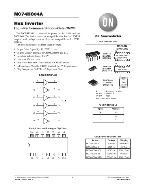
DevicePackage Shipping MC74HC04AN PDIP–142000 / Box MC74HC04AD SOIC–1455 / Rail MC74HC04ADR2SOIC–142500 / Reel MARKING DIAGRAMSA = Assembly Location WL or L = Wafer Lot YY or Y = YearWW or W = Work WeekMC74HC04ADT TSSOP–1496 / Rail MC74HC04ADTR2TSSOP–142500 / ReelTSSOP–14DT SUFFIX CASE 948GHC 04A ALYW114114PDIP–14N SUFFIX CASE 646MC74HC04AN AWLYYWW SOIC–14D SUFFIX CASE 751A114HC04A AWLYWW L HFUNCTION TABLEInputsOutputsA H LYON Semiconductor and are trademarks of Semiconductor Components Industries, LLC (SCILLC). SCILLC reserves the right to make changes without further notice to any products herein. SCILLC makes no warranty, representation or guarantee regarding the suitability of its products for any particular purpose, nor does SCILLC assume any liability arising out of the application or use of any product or circuit, and specifically disclaims any and all liability, including without limitation special, consequential or incidental damages. “Typical” parameters which may be provided in SCILLC data sheets and/or specifications can and do vary in different applications and actual performance may vary over time. All operating parameters, including “Typicals” must be validated for each customer application by customer’s technical experts. SCILLC does not convey any license under its patent rights nor the rights of others.SCILLC products are not designed, intended, or authorized for use as components in systems intended for surgical implant into the body, or other applications intended to support or sustain life, or for any other application in which the failure of the SCILLC product could create a situation where personal injury or death may occur. Should Buyer purchase or use SCILLC products for any such unintended or unauthorized application, Buyer shall indemnify and hold SCILLC and its officers, employees, subsidiaries, affiliates, and distributors harmless against all claims, costs, damages, and expenses, and reasonable attorney fees arising out of, directly or indirectly, any claim of personal injury or death associated with such unintended or unauthorized use, even if such claim alleges that SCILLC was negligent regarding the design or manufacture of the part. SCILLC is an Equal Opportunity/Affirmative Action Employer. PUBLICATION ORDERING INFORMATIONCENTRAL/SOUTH AMERICA:Spanish Phone:303–308–7143 (Mon–Fri 8:00am to 5:00pm MST)Email:ONlit–spanish@ASIA/PACIFIC: LDC for ON Semiconductor – Asia SupportPhone:303–675–2121 (Tue–Fri 9:00am to 1:00pm, Hong Kong Time)Toll Free from Hong Kong & Singapore:001–800–4422–3781Email: ONlit–asia@JAPAN: ON Semiconductor, Japan Customer Focus Center4–32–1 Nishi–Gotanda, Shinagawa–ku, Tokyo, Japan 141–8549Phone: 81–3–5740–2745Email: r14525@。
74HC04真值表及参数
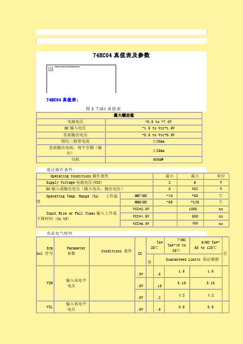
74HC04真值表及参数74HC04真值表:图3 7404真值表最大额定值电源电压-0.5 to +7.0VDC输入电压-1.5 to Vcc+1.5V直流输出电压-0.5 to Vcc+0.5V钳位二极管电流±20mA直流输出电流,每个引脚(输出)±25mA功耗600mW建议操作条件:Operating Conditions操作条件最小最大单位Supply Voltage电源电压(VCC) 2 6 V DC输入或输出电压(输入电压,输出电压)0 VCC VOperating Temp. Range (TA) 工作温度MM74HC-40 +85 ℃MM54HC -55 +125 ℃Input Rise or Fall Times输入上升或下降时间 (tr,tf)VCC=2.0V 1000 ns VCC=4.5V500ns VCC=6.0V 400 ns直流电气特性Sym bol 符号Parameter参数Conditions 条件VCCTA=25℃74HCTA=-40 to85℃54HC TA=-55 to 125℃单位典型Guaranteed Limits 保证极限VIH 输入高电平电压2.0V1.51.5 1.5V4.5V3.153.15 3.156.0V4.24.2 4.2VIL 输入低电平电压2.0V.50.5 0.5 V4 .5V1.351.35 1.356 .0V1.81.8 1.8VOH 输出高电平电压VIN=VIL 丨IOUT丨≤20 μA2.0V2.01.91.9 1.9V4.5V4.54.44.4 4.46.0V6.05.95.9 5.9VIN=VIL 丨IOUT丨≤4.0 mA 丨IOUT丨≤5.2 mA4.5V4.23.983.84 3.7V6.0V5.75.485.34 5.2VOL 输出低电平电压VIN=VIH 丨IOUT丨≤20 μA2.0V00.10.1 0.1V4.5V00.10.1 0.16.0V.10.10.1VIN=VIH 丨IOUT丨≤4.0 mA 丨IOUT丨≤5.2 mA4.5V.2.260.33 0.4V6.0V.2.260.330.4IIN 最大输入电流VIN=VCC or GND6.0V±0.1±1.0 ±1.0μAICC 电源电流VIN=VCC or GNDIOUT=0 μA6.0V2.020 40μA交流电气特性:Symbol 符号Parameter 参数条件典型Guaranteed Limit 保证极限单位tPHL,tPLH 最高传播延迟时间8 15 ns AC Electrical Characteristics VCCe2.0V to 6.0V, CLe50 pF, tretfe6 ns(unless otherwise specified)交流电气特性:Symbo l 符号Parameter参数Conditions条件VCCTA=25℃TA eb40 to85℃TA eb55 to125℃单位型保证界限tPHL, tPLH 最大传输延迟时间2.0V 595120 145ns4.5V11924296.0V1620 24tTLH, tTHLMaximumOutput Rise and2.0V 07595 110nsFall Time最大输出上升和下降时间4.5V1519 226.0V131619CPDPowerDissipationCapacitance(Note 5)功耗电容(pergate) 0pFCIN 最大输入电容110 10pF。
用非门74HC04与无源晶振产生时钟信号的两种电路
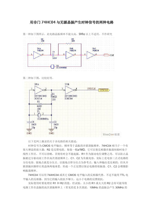
用非门74HC04与无源晶振产生时钟信号的两种电路第一种如下图所示,此电路晶振频率不能太高,5Mhz以上不适用。
不作研究第二种如下图,比较好用。
以下是网上摘录的关于该电路的相关描述:时钟信号为CMOS电平输出,频率等于晶振的并联谐振频率。
74HC04相当于一个有很大增益的放大器;R2是反馈电阻,取值一般≥1MΩ,它可以使反相器在振荡初始时处于线性工作区,不可以省略,否则有时会不能起振。
R1作为驱动电位调整之用,可以防止晶振被过分驱动而工作在高次谐波频率上。
C1、C2为负载电容,实际上是电容三点式电路的分压电容,接地点就是分压点。
以接地点即分压点为参考点,输入和输出是反相的,但从并联谐振回路即石英晶体两端来看,形成一个正反馈以保证电路持续振荡。
C1、C2会稍微影响振荡频率。
74HC04可以用74AHC04或其它CMOS电平输入的反相器代替,不过不能用TTL电平输入的反相器,因为它的输入阻抗不够大,远小于电路的反馈阻抗。
实际使用时要处理好R1和R2的值,经试验,太小的R1或太大的R2会有可能导致电路工作在晶振的高次谐振频率上(常见的是3次谐波,10MHz的晶振会产生30MHz的频率输出)。
对于10MHz的晶振,采用R1=220Ω、R2=1MΩ可以使电路稳定输出10MHz 的方波时钟信号。
晶振电路用反向器(74LS00)与晶振、两个小电容、一个大电阻。
用的是典型电路,可在示波器上就是不振?HC的或HCT的才行,如果电容小的话,应该用MOS输入的门。
LS芯片的最高截止频率没问题,原因是LS芯片需一个百欧级偏置电阻才能达到线性状态,此时增益又不够。
HC和LS速度上并无区别(最大40兆),问题出在振荡电路是将非门当成线性反向放大器来使用。
HC只要加个10兆电阻即可,此时仍有足够的放大倍数(约100)。
LS加个1兆电阻仍是非线性状态,不可能振荡,需要5千才能线性,但此时负反馈太深,放大倍数过小(小于10),仍不可能振荡。
高性能硅门CMOS74HC04芯片说明书
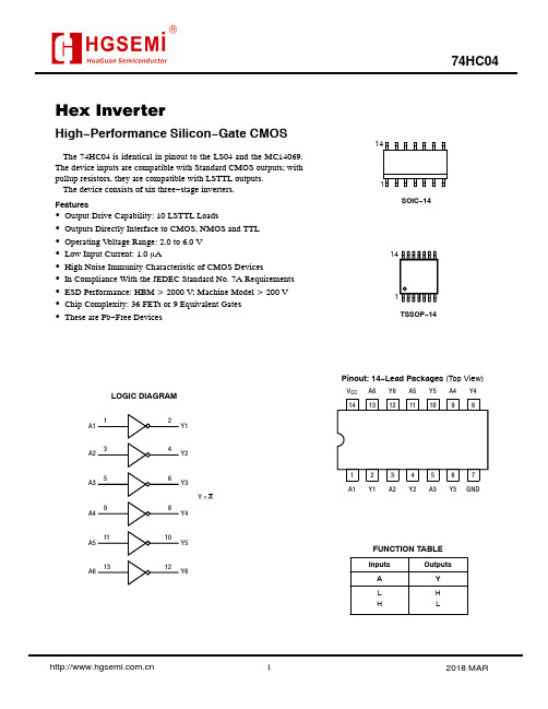
Hex InverterHigh −Performance Silicon −Gate CMOSThe 74HC04 is identical in pinout to the LS04 and the MC14069.The device inputs are compatible with Standard CMOS outputs; with pullup resistors, they are compatible with LSTTL outputs.The device consists of six three −stage inverters.Features•Output Drive Capability: 10 LSTTL Loads•Outputs Directly Interface to CMOS, NMOS and TTL •Operating V oltage Range: 2.0 to 6.0 V •Low Input Current: 1.0 m A•High Noise Immunity Characteristic of CMOS Devices•In Compliance With the JEDEC Standard No. 7A Requirements •ESD Performance: HBM > 2000 V; Machine Model > 200 V •Chip Complexity: 36 FETs or 9 Equivalent Gates •These are Pb −Free DevicesLOGIC DIAGRAMY1A1A2A3A4A5A6Y2Y3Y4Y5Y6Y = APinout: 14−Lead Packages (Top View)1314121110982134567V CC A6Y6A5Y5A4Y4A1Y1A2Y2A3Y3GNDTSSOP −14SOIC −14114114L HFUNCTION TABLEInputsOutputsA H LYMAXIMUM RATINGSSymbol Parameter Value Unit V CC DC Supply Voltage (Referenced to GND)– 0.5 to + 7.0V V in DC Input Voltage (Referenced to GND)– 0.5 to V CC + 0.5V V out DC Output Voltage (Referenced to GND)– 0.5 to V CC + 0.5VI in DC Input Current, per Pin±20mAI out DC Output Current, per Pin±25mAI CC DC Supply Current, V CC and GND Pins±50mAP D Power Dissipation in Still Air,SOIC Package†TSSOP Package†500450mWT stg Storage Temperature– 65 to + 150_C T L Lead Temperature, 1 mm from Case for 10 SecondsSOIC or TSSOP Package260_CStresses exceeding Maximum Ratings may damage the device. Maximum Ratings are stress ratings only. Functional operation above the Recommended Operating Conditions is not implied. Extended exposure to stresses above the Recommended Operating Conditions may affect device reliability.*This device contains protection circuitry to guard against damage due to high static voltages or electric fields. However, precautions must be taken to avoid applications of any voltage higher than maximum rated voltages to this high−impedance circuit. For proper operation, V in and V out should be constrained to the range GND v (V in or V out) v V CC. Unused inputs must always be tied to an appropriate logic voltage level (e.g., either GND or V CC). Unused outputs must be left open.†Derating−SOIC Package: – 7 mW/_C from 65_ to 125_CTSSOP Package: − 6.1 mW/_C from 65_ to 125_CFor high frequency or heavy load considerations, see Chapter 2 of the ON Semiconductor High−Speed CMOS Data Book (DL129/D).RECOMMENDED OPERATING CONDITIONSSymbol Parameter Min Max Unit V CC DC Supply Voltage (Referenced to GND) 2.0 6.0VV in, V out DC Input Voltage, Output Voltage (Referenced to GND)0V CC V T A Operating Temperature, All Package Types– 55+ 125_Ct r, t f Input Rise and Fall Time V CC = 2.0 V (Figure 1)V CC = 4.5 VV CC = 6.0 V 01000500400nsDC CHARACTERISTICS(Voltages Referenced to GND)V CC (V)Guaranteed LimitSymbol Parameter Condition−55 to 25°C≤85°C≤125°C UnitV IH Minimum High−Level InputVoltage V out = 0.1V or V CC−0.1V|I out| ≤ 20m A2.03.04.56.01.502.103.154.201.502.103.154.201.502.103.154.20VV IL Maximum Low−Level InputVoltage V out = 0.1V or V CC− 0.1V|I out| ≤ 20m A2.03.04.56.00.500.901.351.800.500.901.351.800.500.901.351.80VV OH Minimum High−Level OutputVoltage V in = V IH or V IL|I out| ≤ 20m A2.04.56.01.94.45.91.94.45.91.94.45.9V V in =V IH or V IL|I out| ≤ 2.4mA|I out| ≤ 4.0mA |I out| ≤ 5.2mA 3.04.56.02.483.985.482.343.845.342.203.705.20V OL Maximum Low−Level OutputVoltage V in = V IH or V IL|I out| ≤ 20m A2.04.56.00.10.10.10.10.10.10.10.10.1VV in = V IH or V IL|I out| ≤ 2.4mA|I out| ≤ 4.0mA|I out| ≤ 5.2mA3.04.56.00.260.260.260.330.330.330.400.400.40I in Maximum Input LeakageCurrentV in = V CC or GND 6.0±0.1±1.0±1.0m AI CC Maximum Quiescent SupplyCurrent (per Package)V in = V CC or GNDI out = 0m A6.0 2.02040m ANOTE:Information on typical parametric values can be found in Chapter 2 of the ON Semiconductor High−Speed CMOS Data Book (DL129/D). AC CHARACTERISTICS(C L = 50pF, Input t r = t f = 6ns)V CC (V)Guaranteed LimitSymbol Parameter−55 to 25°C≤85°C≤125°C Unitt PLH, t PHL Maximum Propagation Delay, Input A or B to Output Y(Figures 1 and 2)2.03.04.56.07530151395401916110552219nst TLH, t THL Maximum Output Transition Time, Any Output(Figures 1 and 2)2.03.04.56.07527151395321916110362219nsC in Maximum Input Capacitance101010pF NOTE:For propagation delays with loads other than 50 pF, and information on typical parametric values, see Chapter 2 of the ON Semiconductor High−Speed CMOS Data Book (DL129/D).C PD Power Dissipation Capacitance (Per Inverter)*Typical @ 25°C, V CC = 5.0 VpF20*Used to determine the no−load dynamic power consumption: P D = C PD V CC2f + I CC V CC. For load considerations, see Chapter 2 of the ON Semiconductor High−Speed CMOS Data Book (DL129/D).Figure 1. Switching WaveformsGNDV CCOUTPUT YINPUT AC L **Includes all probe and jig capacitanceTESTFigure 2. Test CircuitYA Figure 3. Expanded Logic Diagram(1/6 of the Device Shown)。
74HC04D中文资料_数据手册_参数
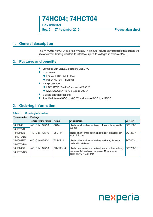
Output nY H L
Table 4. Limiting values In accordance with the Absolute Maximum Rating System (IEC 60134). Voltages are referenced to GND (ground = 0 V).
3 of 15
Nexperia
74HC04; 74HCT04
Hex inverter
8. Recommended operating conditions
Table 5. Recommended operating conditions Voltages are referenced to GND (ground = 0 V)
-
50
65
[2]
-
50 mA - mA +150 C 500 mW
[1] The input and output voltage ratings may be exceeded if the input and output current ratings are observed.
[2] For SO14 package: Ptot derates linearly with 8 mW/K above 70 C. For (T)SSOP14 packages: Ptot derates linearly with 5.5 mW/K above 60 C. For DHVQFN14 packages: Ptot derates linearly with 4.5 mW/K above 60 C.
-
3.15
-V
VCC = 6.0 V
74HC04DB-T中文资料

PINNING PIN 1 2 3 4 5 6 7 8 9 10 11 12 13 14 SYMBOL 1A 1Y 2A 2Y 3A 3Y GND 4Y 4A 5Y 5A 6Y 6A VCC DESCRIPTION data input data output data input data output data input data output ground (0 V) data output data input data output data input data output data input supply voltage Fig.1 Pin configuration DIP14, SO14 and (T)SSOP14.
2003 Jul 23
2
元器件交易网
Philips Semiconductors
Product specification
Hex inverter
ORDERING INFORMATION PACKAGE TYPE NUMBER TEMPERATURE RANGE 74HC04N 74HCT04N 74HC04D 74HCT04D 74HC04DB 74HCT04DB 74HC04PW 74HCT04PW 74HC04BQ 74HCT04BQ −40 to +125 °C −40 to +125 °C −40 to +125 °C −40 to +125 °C −40 to +125 °C −40 to +125 °C −40 to +125 °C −40 to +125 °C −40 to +125 °C −40 to +125 °C PINS 14 14 14 14 14 14 14 14 14 14 PACKAGE DIP14 DIP14 SO14 SO14 SSOP14 SSOP14 TSSOP14 TSSOP14 DHVQFN14 DHVQFN14
74HC1G04数据手册

per input; VCC = 4.5 V to 5.5 V;
Product data sheet
Rev. 04 — 16 July 2007
© NXP B.V. 2007. All rights reserved.
2 of 11
NXP Semiconductors
74HC1G04; 74HCT1G04
Inverter
8. Limiting values
Table 5. Limiting values In accordance with the Absolute Maximum Rating System (IEC 60134). Voltages are referenced to GND (ground = 0 V). [1]
2. Features
I Symmetrical output impedance I High noise immunity I Low power dissipation I Balanced propagation delays I SOT353-1 and SOT753 package options
Description plastic thin shrink small outline package; 5 leads; body width 1.25 mm
plastic surface-mounted package; 5 leads
4. Marking
Version SOT353-1
SOT753
1.5 1.2
-
3.15 2.4
-
4.2 3.2
-
-
0.8 0.5
-
2.1 1.35
AiP74HC04中文资料
VCC=2.0V IO=-20uA
VCC=4.5V IO =-20uA
Vi=VIH 或 VIL
VCC=4.5V IO=-4.0mA
VCC=6.0V IO=-20uA
VCC=6.0V IO=-5.2mA
VCC=2.0V IO=20uA
VCC=4.5V IO=20uA
Vi=VIH 或 VIL
VCC=4.5V IO=4.0mA
江苏省无锡市蠡园经济开发区滴翠路 100 号 9 栋 2 层
http://www.i-core. cn
邮编:214072
第6页共9页 版本:2012-02-A1
表 733-11-I
5、封装尺寸与外形图 5. 1、DIP14 图与封装尺寸
无锡中微爱芯电子有限公司
Wuxi I-CORE Electronics Co., Ltd.
编号:AiP74HC04-AX-BJ-160
6、声明及注意事项:
6.1、产品中有毒有害物质或元素的名称及含量
有毒有害物质或元素
部件名称
铅(Pb)
汞(Hg) 镉(Cd)
六阶铬 多溴联苯 多溴联苯 (C(r Ⅵ)) (PBBs) 醚(PBDEs)
引线框
○
○
○
○
○
○
i-core 塑封树脂 芯片 内引线 装片胶
VCC=6.0V IO=20uA
VCC=6.0V IO=5.2mA
VCC=6.0V Vi= VCC 或 GND
VCC=6.0V Vi=VIH 或 VIL Vo= VCC 或 GND
VCC=6.0V Vi =VCC 或 GND IO=0
最小
1.5 3.15 4.2 - - - 1.9
74系列功能大全(中文)
74HC32 QUAD 2-INPUT OR GATE 四个双端或门
74HC34 NON-INVERTER 非反向器
74HC354 8-CH 3-STATE MUX 8路3态多路器
74HC356 8-CH 3-STATE MUX 8路3态多路器
74HC4020 14-Stage Binary Counter 14输出计数器
74HC4017 Decade Counter/Divider with 10 Decoded Outputs
十进制计数器带10个译码输出端
74HC4040 12 Stage Binary Counter 12出计数器
74HC4046 PHASE LOCK LOOP 相位监测输出器
74HC4049 LEVEL DOWN CONVERTER 电平变低器
74HC4050 LEVEL DOWN CONVERTER 电平变低器
74HC4051 8-CH ANALOG MUX 8通道多路器
74HC4052 4-CH ANALOG MUX 4通道多路器
74HC365 HEX 3-STATE BUFFER 六个三态缓冲门
74HC366 3-STATE BUFFER INVERTER 缓冲反向器
74HC367 3-STATE BUFFER INVERTER 缓冲反向器
74HC368 3-STATE BUFFER INVERTER 缓冲反向器
74HC42 BCD TO DECIMAL BCD转十进制译码器
74HC423A RETRIGGERABLE MONOSTAB 可重触发单稳
74HC4511 BCD-7 SEG DRIVER/DECODER 7段译码器
FAIRCHILD 74VHC04 数据手册

74VHC04 — Hex InverterHex InverterFeatures■ High Speed: t PD = 3.8ns (typ.) at V CC = 5V ■ High noise immunity: V NIH = V NIL = 28% V CC (min.) ■ Power down protection is provided on all inputs ■ Low Noise: V OLP = 0.4V (typ.)■ Low power dissipation: I CC = 2µA (max.) @ T A = 25°C ■ Pin and function compatible with 74HC04General DescriptionThe VHC04 is an advanced high speed CMOS Inverter fabricated with silicon gate CMOS technology. It achieves the high speed operation similar to equivalent Bipolar Schottky TTL while maintaining the CMOS low power dissipation.The internal circuit is composed of 3 stages including buffer output, which provide high noise immunity and stable output. An input protection circuit ensures that 0V to 7V can be applied to the input pins without regard to the supply voltage. This device can be used to interface 5V to 3V systems and two supply systems such as bat-tery back up. This circuit prevents device destruction due to mismatched supply and input voltages.Ordering InformationDevice also available in Tape and Reel. Specify by appending suffix letter “X” to the ordering number.All packages are lead free per JEDEC: J-STD-020B standard.Order NumberPackage NumberPackage Description74VHC04M M14A 14-Lead Small Outline Integrated Circuit (SOIC), JEDEC MS-012, 0.150" Narrow74VHC04SJ M14D 14-Lead Small Outline Package (SOP), EIAJ TYPE II, 5.3mm Wide 74VHC04MTC MTC1414-Lead Thin Shrink Small Outline Package (TSSOP), JEDEC MO-153, 4.4mm Wide74VHC04NN14A14-Lead Plastic Dual-In-Line Package (PDIP), JEDEC MS-001, 0.300" WidePin DescriptionTruth TablePin Names Description A n InputsO n Outputs A OL HH L74VHC04 — Hex Inverter74VHC04 — Hex InverterRecommended Operating Conditions (1)The Recommended Operating Conditions table defines the conditions for actual device operation. Recommended operating conditions are specified to ensure optimal performance to the datasheet specifications. Fairchild does not recommend exceeding them or designing to absolute maximum ratings.Note:1.Unused inputs must be held HIGH or LOW. They may not float.V CC Supply Voltage –0.5V to +7.0V V IN DC Input Voltage –0.5V to +7.0V V OUT DC Output Voltage –0.5V to V CC + 0.5VI IK Input Diode Current –20mA I OK Output Diode Current ±20mA I OUT DC Output Current ±25mA I CC DC V CC /GND Current ±50mAT STG Storage Temperature–65°C to +150°CT LLead Temperature (Soldering, 10 seconds)260°CSymbol ParameterRatingV CC Supply Voltage 2.0V to +5.5V V IN Input Voltage 0V to +5.5V V OUT Output Voltage 0V to V CCT OPR Operating Temperature –40°C to +85°C t r , t fInput Rise and Fall Time, V CC = 3.3V ± 0.3V V CC = 5.0V ± 0.5V0ns/V ∼ 100ns/V 0ns/V ∼20ns/V74VHC04 — Hex InverterNoise CharacteristicsNote:2.Parameter guaranteed by design.Voltage3.0–5.50.7 x V CC0.7 x V CCV IL LOW Level Input Voltage 2.00.500.50V3.0–5.50.3 x V CC0.3 x V CCV OHHIGH Level Output Voltage2.0V IN = V IH or V ILI OH = –50µA 1.9 2.0 1.9V 3.0 2.9 3.0 2.94.5 4.4 4.54.43.0I OH = –4mA 2.58 2.484.5I OH = –8mA3.943.80V OLLOW Level Output Voltage2.0V IN = V IH or V ILI OL = 50µA 0.00.10.1V3.00.00.10.14.50.00.10.13.0I OL = 4mA 0.360.444.5I OL = 8mA0.360.44I IN Input Leakage Current 0–5.5V IN = 5.5V or GND ±0.1±1.0µA I CCQuiescent Supply Current5.5V IN = V CC or GND2.020.0µASymbolParameterV CC (V)ConditionsT A = 25°CUnitsTyp.LimitsV OLP (2) Quiet Output Maximum Dynamic V OL5.0C L = 50pF 0.40.8V V OLV (2) Quiet Output Minimum Dynamic V OL5.0C L = 50pF –0.4–0.8V V IHD (2) Minimum HIGH Level Dynamic Input Voltage 5.0C L = 50pF 3.5V V ILD (2)Maximum LOW Level Dynamic Input Voltage5.0C L =50pF1.5V74VHC04 — Hex InverterNote:3.C PD is defined as the value of the internal equivalent capacitance which is calculated from the operating current consumption without load. Average operating current can be obtained by the equation: I CC (opr.) = C PD • V CC • f IN + I CC / 6 (per gate).C L = 50 pF 7.510.6 1.012.05.0 ± 0.5C L = 15 pF 3.8 5.5 1.0 6.5ns C L = 50 pF 5.37.5 1.08.5C IN Input Capacitance V CC = OPEN41010pF C PDPower Dissipation Capacitance(3)18pFFigure 1. 14-Lead Small Outline Integrated Circuit (SOIC), JEDEC MS-012, 0.150" NarrowPackage drawings are provided as a service to customers considering Fairchild components. Drawings may change in any manner without notice. Please note the revision and/or date on the drawing and contact a Fairchild Semiconductor representative to verify or LAND PATTERN RECOMMENDATIONNOTES:UNLESS OTHERWISE SPECIFIEDA)THIS PACKAGE CONFORMS TO JEDECMS-012,VARIATION AB,ISSUE C,B)ALL DIMENSIONS ARE IN MILLIMETERS.C)DIMENSIONS DO NOT INCLUDE MOLDFLASH OR BURRS.D)LANDPATTERN STANDARD:SOIC127P600X145-14ME)DRAWING CONFORMS TO ASME Y14.5M-1994F)DRAWING FILE NAME:M14AREV13PIN ONE INDICATOR8°0°SEATING PLANEDETAIL ASCALE:20:1GAGE PLANE 0.25X 45°10.10C CB C A7MSEE DETAIL A1.70 1.276.004.003.80(0.33)1.270.510.351.75MAX1.501.250.250.100.250.19(1.04)0.900.500.36R0.10R0.100.500.25Figure 2. 14-Lead Small Outline Package (SOP), EIAJ TYPE II, 5.3mm WidePackage drawings are provided as a service to customers considering Fairchild components. Drawings may change in any manner without notice. Please note the revision and/or date on the drawing and contact a Fairchild Semiconductor representative to verify orFigure 3. 14-Lead Thin Shrink Small Outline Package (TSSOP), JEDEC MO-153, 4.4mm WidePackage drawings are provided as a service to customers considering Fairchild components. Drawings may change in any manner without notice. Please note the revision and/or date on the drawing and contact a Fairchild Semiconductor representative to verify or obtain the most recent revision. Package specifications do not expand the terms of Fairchild’s worldwide terms and conditions, specifically the warranty therein, which covers Fairchild products.C.DIMENSIONS ARE EXCLUSIVE OF BURRS,MOLD FLASH,AND TIE BAR EXTRUSIONSF.DRAWING FILE NAME:MTC14REV6R0.09min12.00°TOP&BOTTOM1.00D.DIMENSIONING AND TOLERANCES PER ANSI Y14.5M,1982R0.09minNDPATTERN STANDARD:SOP65P640X110-14M 6.101.650.45A.CONFORMS TO JEDEC REGISTRATION MO-153,VARIATION AB,REF NOTE 6B.DIMENSIONS ARE IN MILLIMETERSFigure 4. 14-Lead Plastic Dual-In-Line Package (PDIP), JEDEC MS-001, 0.300" WidePackage drawings are provided as a service to customers considering Fairchild components. Drawings may change in any manner without notice. Please note the revision and/or date on the drawing and contact a Fairchild Semiconductor representative to verify or obtain the most recent revision. Package specifications do not expand the terms of Fairchild’s worldwide terms and conditions, specifically the warranty therein, which covers Fairchild products.71NOTES:UNLESS OTHERWISE SPECIFIEDA)THIS PACKAGE CONFORMS TO JEDEC MS-001VARIATION BAB)ALL DIMENSIONS ARE IN MILLIMETERS.C)DIMENSIONS ARE EXCLUSIVE OF BURRS,MOLD FLASH,AND TIE BAR EXTRUSIONS.D)DIMENSIONS AND TOLERANCES PER ASME Y14.5-1994E)DRAWING FILE NAME:MKT-N14AREV78.127.620.350.203.563.305.33MAX 0.38MIN1.771.140.580.352.543.813.178.82(1.74)subsidiaries,and is not intended to be an exhaustive list of all such trademarks.ACEx ®Build it Now ™CorePLUS ™CROSSVOLT ™CTL™Current Transfer Logic™EcoSPARK ®EZSWITCH™*™®Fairchild®Fairchild Semiconductor ®FACT Quiet Series™FACT ®FAST ®FastvCore ™FlashWriter ®*FPS ™FRFET ®Global Power Resource SM Green FPS ™Green FPS ™e-Series ™GTO ™i-Lo ™IntelliMAX ™ISOPLANAR ™MegaBuck™MICROCOUPLER ™MicroFET ™MicroPak ™MillerDrive™Motion-SPM™OPTOLOGIC ®OPTOPLANAR ®®PDP-SPM™Power220®Power247®POWEREDGE ®Power-SPM ™PowerTrench ®Programmable Active Droop ™QFET ®QS ™QT Optoelectronics ™Quiet Series ™RapidConfigure ™SMART START ™SPM ®STEALTH™SuperFET ™SuperSOT ™-3SuperSOT ™-6SuperSOT ™-8SyncFET™®The Power Franchise ®TinyBoost ™TinyBuck ™TinyLogic ®TINYOPTO ™TinyPower ™TinyPWM ™TinyWire ™µSerDes ™UHC ®Ultra FRFET ™UniFET ™VCX ™*EZSWITCH™and FlashWriter ®are trademarks of System General Corporation,used under license by Fairchild Semiconductor.DISCLAIMERFAIRCHILD SEMICONDUCTOR RESERVES THE RIGHT TO MAKE CHANGES WITHOUT FURTHER NOTICE TO ANY PRODUCTS HEREIN TO IMPROVE RELIABILITY,FUNCTION,OR DESIGN.FAIRCHILD DOES NOT ASSUME ANY LIABILITY ARISING OUT OF THE APPLICATION OR USE OF ANY PRODUCT OR CIRCUIT DESCRIBED HEREIN;NEITHER DOES IT CONVEY ANY LICENSE UNDER ITS PATENT RIGHTS,NOR THE RIGHTS OF OTHERS.THESE SPECIFICATIONS DO NOT EXPAND THE TERMS OF FAIRCHILD’S WORLDWIDE TERMS AND CONDITIONS,SPECIFICALLY THE WARRANTY THEREIN,WHICH COVERS THESE PRODUCTS.LIFE SUPPORT POLICYFAIRCHILD’S PRODUCTS ARE NOT AUTHORIZED FOR USE AS CRITICAL COMPONENTS IN LIFE SUPPORT DEVICES OR SYSTEMS WITHOUT THE EXPRESS WRITTEN APPROVAL OF FAIRCHILD SEMICONDUCTOR CORPORATION.As used herein:1.Life support devices or systems are devices or systems which,(a)are intended for surgical implant into the body or (b)support or sustain life,and (c)whose failure to perform when properly used in accordance with instructions for use provided in the labeling,can be reasonably expected to result in a significant injury of the user.2.A critical component in any component of a life support,device,or system whose failure to perform can be reasonably expected to cause the failure of the life support device or system,or to affect its safety or effectiveness.PRODUCT STATUS DEFINITIONS Definition of Terms Datasheet Identification Product Status DefinitionAdvance InformationForm First Productionative or In DesignThis datasheet contains the design specifications for productdevelopment.Specifications may change in any manner without notice.PreliminaryThis datasheet contains preliminary data;supplementary data will be published at a later date.Fairchild Semiconductor reserves the right to make changes at any time without notice to improve design.74VHC04 — Hex Inverter。
74HC00中文资料(真值表-引脚图-电气参数及应用电路)

2.0
-
1.5
-
-
1.5
-
1.5
-
V
4.5
3.15
-
-
3.15
-
3.15
-
6.0
4.2
-
-
4.2
-
4.2
-
VIL
Low Level Input-
Voltage输入低电平电压
2.0
-
-
-
0.5
-
0.5
-
0.5
-
4.5
-
-
1.35
-
1.35
-
1.35
V
6.0
-
-
1.8
-
1.8
与非门74HC00中文资料(真值表,引脚图,电气参数及应用电路)
74HC00功能:2输入端四与非门
TRUTH TABLE真值表:
A
B
Y
L
L
H
L
H
H
H
L
H
H
H
L
74HC00引脚图及引脚功能表:
管脚位
SYMBOL符号
NAME AND FUNCTION名称及功能
1, 4, 9, 12
1A to 4A
பைடு நூலகம்Data Inputs数据输入
SYMBOL符号
Parameter参数
Value数值
Unit单位
VCC
Supply Voltage电源电压
-0.5 to +7
V
VI
DC Input Voltage直流输入电压
-0.5 to VCC + 0.5
CD74HC04MT资料

For VI < -0.5V or VI > VCC + 0.5V . . . . . . . . . . . . . . . . . . . . . .±20mA DC Output Diode Current, IOK
Low Level Input Voltage
High Level Output Voltage CMOS Loads
High Level Output Voltage TTL Loads
Low Level Output Voltage CMOS Loads
Low Level Output Voltage TTL Loads
The CD54HC04, CD54HCT04, CD74HC04 and CD74HCT04 logic gates utilize silicon-gate CMOS technology to achieve operating speeds similar to LSTTL gates, with the low power consumption of standard CMOS integrated circuits. All devices have the ability to drive 10 LSTTL loads. The 74HCT logic family functionally is pin compatible with the standard 74LS logic family.
HD74HC04RPEL中文资料
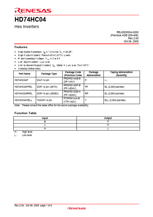
HD74HC04Hex InvertersREJ03D0534-0200(Previous ADE-205-406)Rev.2.00Oct 06, 2005 Features• High Speed Operation: t pd = 7.5 ns typ (C L = 50 pF)• High Output Current: Fanout of 10 LSTTL Loads• Wide Operating Voltage: V CC = 2 to 6 V• Low Input Current: 1 µA max• Low Quiescent Supply Current: I CC (static) = 1 µA max (Ta = 25°C)• Ordering InformationPart Name Package TypePackage Code(Previous Code)PackageAbbreviationTaping Abbreviation(Quantity)HD74HC04P DILP-14pin PRDP0014AB-B(DP-14AV)P —HD74HC04FPEL SOP-14 pin (JEITA) PRSP0014DF-B(FP-14DAV)FP EL (2,000 pcs/reel)HD74HC04RPEL SOP-14 pin (JEDEC) PRSP0014DE-A(FP-14DNV)RP EL (2,500 pcs/reel)HD74HC04TELL TSSOP-14pin PTSP0014JA-B(TTP-14DV)T ELL(2,000pcs/reel)Note: Please consult the sales office for the above package availability.Function TableInput OutputA YL HH L H : High levelL : Low levelPin ArrangementAbsolute Maximum RatingsItem Symbol Ratings UnitSupply voltage range V CC –0.5 to 7.0 V Input / Output voltage Vin, Vout –0.5 to V CC +0.5VInput / Output diode current I IK , I OK ±20 mAOutput current I O±25 mAV CC , GND current I CC or I GND ±50 mAPower dissipationP T 500 mWStorage temperature Tstg –65 to +150 °CNote: The absolute maximum ratings are values, which must not individually be exceeded, and furthermore, no two ofwhich may be realized at the same time.Recommended Operating ConditionsItem Symbol Ratings Unit ConditionsSupply voltage V CC 2 to 6 V Input / Output voltage V IN , V OUT 0 to V CC V Operating temperature Ta –40 to 85 °C 0 to 1000 V CC = 2.0 V 0 to 500V CC = 4.5 V Input rise / fall time *1t r , t f0 to 400nsV CC = 6.0 VNote: 1. This item guarantees maximum limit when one input switches. Waveform: Refer to test circuit of switching characteristics.Electrical CharacteristicsTa = 25°CTa = –40 to+85°CItem Symbol V CC (V) Min Typ Max Min Max UnitTest Conditions2.0 1.5 — — 1.5 — 4.53.15 — — 3.15 —V IH 6.0 4.2 — — 4.2 —V2.0 — — 0.5 — 0.5 4.5 — — 1.35 — 1.35Input voltage V IL6.0 — — 1.8 — 1.8 V 2.0 1.9 2.0 — 1.9 — 4.5 4.4 4.5 — 4.4 — 6.0 5.9 6.0 — 5.9 — I OH = –20 µA 4.5 4.18 — — 4.13 — I OH = –4 mA V OH6.0 5.68 — — 5.63 —V Vin = V IH or V IL I OH = –5.2 mA2.0 — 0.0 0.1 — 0.1 4.5 — 0.0 0.1 — 0.1 6.0 — 0.0 0.1 — 0.1 I OL = 20 µA 4.5 — — 0.26 — 0.33I OL = 4 mAOutput voltage V OL6.0 — — 0.26 — 0.33 V Vin = V IH or V IL I OL = 5.2 mA Input current Iin6.0 — — ±0.1 — ±1.0 µA Vin = V CC or GNDQuiescent supplycurrent I CC 6.0 — — 1.0 — 10 µA Vin = V CC or GND, Iout = 0 µASwitching Characteristics (C L = 50 pF, Input t r = t f = 6 ns)Ta = 25°CTa = –40 to +85°CItem Symbol V CC (V) Min Typ Max Min Max UnitTest Conditions2.0 — — 90 — 115 4.5 — 7 18 — 23t PLH 6.0 — — 15 — 20ns 2.0 — — 90 — 115 4.5 — 8 18 — 23 Propagation delay time t PHL6.0 — — 15 — 20ns 2.0 — — 75 — 95 4.5 — 5 15 — 19 Output rise time t TLH6.0 — — 13 — 16ns 2.0 — — 75 — 95 4.5 — 5 15 — 19 Output fall timet THL6.0 — — 13 — 16 ns Input capacitance Cin— — 5 10 — 10 pFTest CircuitWaveformsPackage Dimensions RENESAS SALES OFFICESRefer to "/en/network" for the latest and detailed information.Renesas Technology America, Inc.450 Holger Way, San Jose, CA 95134-1368, U.S.ATel: <1> (408) 382-7500, Fax: <1> (408) 382-7501Renesas Technology Europe LimitedDukes Meadow, Millboard Road, Bourne End, Buckinghamshire, SL8 5FH, U.K.Tel: <44> (1628) 585-100, Fax: <44> (1628) 585-900Renesas Technology Hong Kong Ltd.7th Floor, North Tower, World Finance Centre, Harbour City, 1 Canton Road, Tsimshatsui, Kowloon, Hong KongTel: <852> 2265-6688, Fax: <852> 2730-6071Renesas Technology Taiwan Co., Ltd.10th Floor, No.99, Fushing North Road, Taipei, TaiwanTel: <886> (2) 2715-2888, Fax: <886> (2) 2713-2999Renesas Technology (Shanghai) Co., Ltd.Unit2607 Ruijing Building, No.205 Maoming Road (S), Shanghai 200020, ChinaTel: <86> (21) 6472-1001, Fax: <86> (21) 6415-2952Renesas Technology Singapore Pte. Ltd.1 Harbour Front Avenue, #06-10, Keppel Bay Tower, Singapore 098632Tel: <65> 6213-0200, Fax: <65> 6278-8001Renesas Technology Korea Co., Ltd.Kukje Center Bldg. 18th Fl., 191, 2-ka, Hangang-ro, Yongsan-ku, Seoul 140-702, KoreaTel: <82> 2-796-3115, Fax: <82> 2-796-2145Renesas Technology Malaysia Sdn. Bhd.Unit 906, Block B, Menara Amcorp, Amcorp Trade Centre, No.18, Jalan Persiaran Barat, 46050 Petaling Jaya, Selangor Darul Ehsan, MalaysiaTel: <603> 7955-9390, Fax: <603> 7955-9510。
IN74HC04A中文资料

2.0 4.5 6.0 2.0 4.5 6.0 -
95 19 16 95 19 16 10
110 22 19 110 22 19 10
ns
tTLH, tTHL
ns
CIN
pF
Typical @25°C,VCC=5.0 V 20 pF
CPD
Used to determine the no-load dynamic power consumption: PD=CPDVCC2f+ICCVCC
RECOMMENDED OPERATING CONDITIONS
Symbol VCC VIN, VOUT TA tr, tf Parameter DC Supply Voltage (Referenced to GND) DC Input Voltage, Output Voltage (Referenced to GND) Operating Temperature, All Package Types Input Rise and Fall Time (Figure 1) VCC =2.0 V VCC =4.5 V VCC =6.0 V Min 2.0 0 -55 0 0 0 Max 6.0 VCC +125 1000 500 400 Unit V V °C ns
tPLH, tPHL
Maximum Propagation Delay, Input A to Output Y (Figures 1 and 2) Maximum Output Transition Time, Any Output (Figures 1 and 2) Maximum Input Capacitance Power Dissipation Capacitance (Per Inverter)
- 1、下载文档前请自行甄别文档内容的完整性,平台不提供额外的编辑、内容补充、找答案等附加服务。
- 2、"仅部分预览"的文档,不可在线预览部分如存在完整性等问题,可反馈申请退款(可完整预览的文档不适用该条件!)。
- 3、如文档侵犯您的权益,请联系客服反馈,我们会尽快为您处理(人工客服工作时间:9:00-18:30)。
Pb-Free 14-Lead Small Outline Integrated Circuit (SOIC), JEDEC MS-012, 0.150" Narrow
MM74HC04SJ
M14D Pb-Free 14-Lead Small Outline Package (SOP), EIAJ TYPE II, 5.3mm Wide
Units
ns ns ns ns ns ns pF
pF
3
MM74HC04
Physical Dimensions inches (millimeters) unless otherwise noted
14-Lead Small Outline Integrated Circuit (SOIC), JEDEC MS-012, 0.150" Narrow Package Number M14A
Output Voltage
|IOUT| ≤ 20 µA
2.0V
2.0
1.9
1.9
4.5V
4.5
4.4
4.4
1.9
V
4.4
V
6.0V
6.0
5.9
5.9
5.9
V
VIN = VIL
|IOUT| ≤ 4.0 mA
|IOUT| ≤ 5.2 mA
VOL
Maximum LOW Level VIN = VIH
Output Voltage
Input Voltage
2.0V 4.5V
1.5
1.5
3.15
3.ห้องสมุดไป่ตู้5
1.5
V
3.15
V
6.0V
4.2
4.2
4.2
V
VIL
Maximum LOW Level
Input Voltage
2.0V 4.5V
0.5
0.5
1.35
1.35
0.5
V
1.35
V
6.0V
1.8
1.8
1.8
V
VOH
Minimum HIGH Level VIN = VIL
10
10
Note 5: CPD determines the no load dynamic power consumption, PD = CPD VCC2 f + ICC VCC, and the no load dynamic current consumption, IS = CPD VCC f + ICC.
Features
s Typical propagation delay: 8 ns s Fan out of 10 LS-TTL loads s Quiescent power consumption: 10 µW maximum at
room temperature s Low input current: 1 µA maximum
MM74HC04
Absolute Maximum Ratings(Note 1)
(Note 2)
Supply Voltage (VCC) DC Input Voltage (VIN) DC Output Voltage (VOUT) Clamp Diode Current (IIK, IOK) DC Output Current, per pin (IOUT) DC VCC or GND Current, per pin (ICC) Storage Temperature Range (TSTG) Power Dissipation (PD)
Input Rise or Fall Times
(tr, tf) VCC = 2.0V
1000 ns
VCC = 4.5V
500 ns
VCC = 6.0V
400 ns
Note 1: Absolute Maximum Ratings are those values beyond which dam-
age to the device may occur.
4.5V
0.2
0.26
6.0V
0.2
0.26
6.0V
±0.1
0.33 0.33 ±1.0
0.4
V
0.4
V
±1.0
µA
ICC
Maximum Quiescent
VIN = VCC or GND
6.0V
2.0
20
40
µA
Supply Current
IOUT = 0 µA
Note 4: For a power supply of 5V ±10% the worst case output voltages (VOH, and VOL) occur for HC at 4.5V. Thus the 4.5V values should be used when designing with this supply. Worst case VIH and VIL occur at VCC=5.5V and 4.5V respectively. (The VIH value at 5.5V is 3.85V.) The worst case leakage current (IIN, ICC, and IOZ) occur for CMOS at the higher voltage and so the 6.0V values should be used.
4
MM74HC04
Physical Dimensions inches (millimeters) unless otherwise noted (Continued)
2
MM74HC04
AC Electrical Characteristics
VCC = 5V, TA = 25°C, CL = 15 pF, tr = tf = 6 ns
Symbol
Parameter
tPHL, tPLH
Maximum Propagation Delay
Ordering Code:
Order Number
Package Number
Package Description
MM74HC04M
M14A 14-Lead Small Outline Integrated Circuit (SOIC), JEDEC MS-012, 0.150" Narrow
MM74HC04M_NL
Devices also available in Tape and Reel. Specify by appending the suffix letter “X” to the ordering code. Pb-Free package per JEDEC J-STD-020B.
Connection Diagram
Logic Diagram
Pin Assignments for DIP, SOIC, SOP and TSSOP
1 of 6 Inverters
Top View © 2005 Fairchild Semiconductor Corporation DS005069
MM74HC04 Hex Inverter
September 1983 Revised January 2005
MM74HC04 Hex Inverter
General Description
The MM74HC04 inverters utilize advanced silicon-gate CMOS technology to achieve operating speeds similar to LS-TTL gates with the low power consumption of standard CMOS integrated circuits.
The MM74HC04 is a triple buffered inverter. It has high noise immunity and the ability to drive 10 LS-TTL loads. The 74HC logic family is functionally as well as pin-out compatible with the standard 74LS logic family. All inputs are protected from damage due to static discharge by internal diode clamps to VCC and ground.
600 mW 500 mW
260°C
Recommended Operating Conditions
Min Max Units
Supply Voltage (VCC)
2
6
V
DC Input or Output Voltage
0 VCC V
(VIN, VOUT)
Operating Temperature Range (TA) −40 +85 °C
MM74HC04N
N14A 14-Lead Plastic Dual-In-Line Package (PDIP), JEDEC MS-001, 0.300" Wide
MM74HC04N_NL
N14A Pb-Free 14-Lead Plastic Dual-In-Line Package (PDIP), JEDEC MS-001, 0.300" Wide
MM74HC04MTC
MTC14 14-Lead Thin Shrink Small Outline Package (TSSOP), JEDEC MO-153, 4.4mm Wide
