sn74lvc1g14-施密特触发器
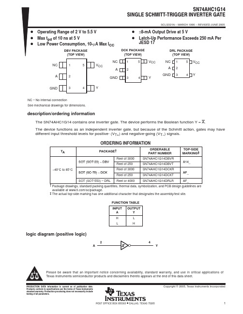
sn74ahc1g14单路施密特触发反向器
PACKAGING INFORMATIONOrderable Device Status (1)Package Type PackageDrawing Pins Package Qty Eco Plan (2)Lead/Ball FinishMSL Peak Temp (3)Samples(Requires Login)SN74AHC1G14DBVR ACTIVE SOT-23DBV53000Green (RoHS& no Sb/Br)CU NIPDAU Level-1-260C-UNLIMSN74AHC1G14DBVRE4ACTIVE SOT-23DBV53000Green (RoHS& no Sb/Br)CU NIPDAU Level-1-260C-UNLIMSN74AHC1G14DBVRG4ACTIVE SOT-23DBV53000Green (RoHS& no Sb/Br)CU NIPDAU Level-1-260C-UNLIMSN74AHC1G14DBVT ACTIVE SOT-23DBV5250Green (RoHS& no Sb/Br)CU NIPDAU Level-1-260C-UNLIMSN74AHC1G14DBVTE4ACTIVE SOT-23DBV5250Green (RoHS& no Sb/Br)CU NIPDAU Level-1-260C-UNLIMSN74AHC1G14DBVTG4ACTIVE SOT-23DBV5250Green (RoHS& no Sb/Br)CU NIPDAU Level-1-260C-UNLIMSN74AHC1G14DCKR ACTIVE SC70DCK53000Green (RoHS& no Sb/Br)CU NIPDAU Level-1-260C-UNLIMSN74AHC1G14DCKRE4ACTIVE SC70DCK53000Green (RoHS& no Sb/Br)CU NIPDAU Level-1-260C-UNLIMSN74AHC1G14DCKRG4ACTIVE SC70DCK53000Green (RoHS& no Sb/Br)CU NIPDAU Level-1-260C-UNLIMSN74AHC1G14DCKT ACTIVE SC70DCK5250Green (RoHS& no Sb/Br)CU NIPDAU Level-1-260C-UNLIMSN74AHC1G14DCKTE4ACTIVE SC70DCK5250Green (RoHS& no Sb/Br)CU NIPDAU Level-1-260C-UNLIMSN74AHC1G14DCKTG4ACTIVE SC70DCK5250Green (RoHS& no Sb/Br)CU NIPDAU Level-1-260C-UNLIMSN74AHC1G14DRLR ACTIVE SOT DRL54000Green (RoHS& no Sb/Br)CU NIPDAU Level-1-260C-UNLIMSN74AHC1G14DRLRG4ACTIVE SOT DRL54000Green (RoHS& no Sb/Br)CU NIPDAU Level-1-260C-UNLIM(1) The marketing status values are defined as follows:ACTIVE: Product device recommended for new designs.LIFEBUY: TI has announced that the device will be discontinued, and a lifetime-buy period is in effect.NRND: Not recommended for new designs. Device is in production to support existing customers, but TI does not recommend using this part in a new design. PREVIEW: Device has been announced but is not in production. Samples may or may not be available.OBSOLETE: TI has discontinued the production of the device.Addendum-Page 1(2) Eco Plan - The planned eco-friendly classification: Pb-Free (RoHS), Pb-Free (RoHS Exempt), or Green (RoHS & no Sb/Br) - please check /productcontent for the latest availability information and additional product content details.TBD: The Pb-Free/Green conversion plan has not been defined.Pb-Free (RoHS): TI's terms "Lead-Free" or "Pb-Free" mean semiconductor products that are compatible with the current RoHS requirements for all 6 substances, including the requirement that lead not exceed 0.1% by weight in homogeneous materials. Where designed to be soldered at high temperatures, TI Pb-Free products are suitable for use in specified lead-free processes.Pb-Free (RoHS Exempt): This component has a RoHS exemption for either 1) lead-based flip-chip solder bumps used between the die and package, or 2) lead-based die adhesive used between the die and leadframe. The component is otherwise considered Pb-Free (RoHS compatible) as defined above.Green (RoHS & no Sb/Br): TI defines "Green" to mean Pb-Free (RoHS compatible), and free of Bromine (Br) and Antimony (Sb) based flame retardants (Br or Sb do not exceed 0.1% by weight in homogeneous material)(3) MSL, Peak Temp. -- The Moisture Sensitivity Level rating according to the JEDEC industry standard classifications, and peak solder temperature.Important Information and Disclaimer:The information provided on this page represents TI's knowledge and belief as of the date that it is provided. TI bases its knowledge and belief on information provided by third parties, and makes no representation or warranty as to the accuracy of such information. Efforts are underway to better integrate information from third parties. TI has taken and continues to take reasonable steps to provide representative and accurate information but may not have conducted destructive testing or chemical analysis on incoming materials and chemicals. TI and TI suppliers consider certain information to be proprietary, and thus CAS numbers and other limited information may not be available for release.In no event shall TI's liability arising out of such information exceed the total purchase price of the TI part(s) at issue in this document sold by TI to Customer on an annual basis.Addendum-Page 2TAPE AND REEL INFORMATION*All dimensions are nominal Device Package Type Package DrawingPinsSPQ Reel Diameter (mm)Reel Width W1(mm)A0(mm)B0(mm)K0(mm)P1(mm)W (mm)Pin1Quadrant SN74AHC1G14DBVR SOT-23DBV 53000178.09.0 3.23 3.17 1.37 4.08.0Q3SN74AHC1G14DBVR SOT-23DBV 53000178.09.2 3.3 3.2 1.55 4.08.0Q3SN74AHC1G14DBVR SOT-23DBV 53000180.09.2 3.17 3.23 1.37 4.08.0Q3SN74AHC1G14DBVT SOT-23DBV 5250178.09.0 3.23 3.17 1.37 4.08.0Q3SN74AHC1G14DBVT SOT-23DBV 5250180.09.2 3.17 3.23 1.37 4.08.0Q3SN74AHC1G14DBVT SOT-23DBV 5250178.09.2 3.3 3.2 1.55 4.08.0Q3SN74AHC1G14DCKR SC70DCK 53000180.09.2 2.3 2.55 1.2 4.08.0Q3SN74AHC1G14DCKR SC70DCK 53000178.09.2 2.4 2.4 1.22 4.08.0Q3SN74AHC1G14DCKR SC70DCK 53000178.09.0 2.4 2.5 1.2 4.08.0Q3SN74AHC1G14DCKT SC70DCK 5250178.09.0 2.4 2.5 1.2 4.08.0Q3SN74AHC1G14DCKT SC70DCK 5250180.09.2 2.3 2.55 1.2 4.08.0Q3SN74AHC1G14DCKT SC70DCK 5250178.09.2 2.4 2.4 1.22 4.08.0Q3SN74AHC1G14DRLR SOT DRL 54000180.08.4 1.98 1.780.69 4.08.0Q3*All dimensions are nominalDevice Package Type Package Drawing Pins SPQ Length(mm)Width(mm)Height(mm) SN74AHC1G14DBVR SOT-23DBV53000180.0180.018.0 SN74AHC1G14DBVR SOT-23DBV53000180.0180.018.0 SN74AHC1G14DBVR SOT-23DBV53000205.0200.033.0 SN74AHC1G14DBVT SOT-23DBV5250180.0180.018.0 SN74AHC1G14DBVT SOT-23DBV5250205.0200.033.0 SN74AHC1G14DBVT SOT-23DBV5250180.0180.018.0 SN74AHC1G14DCKR SC70DCK53000205.0200.033.0 SN74AHC1G14DCKR SC70DCK53000180.0180.018.0 SN74AHC1G14DCKR SC70DCK53000180.0180.018.0 SN74AHC1G14DCKT SC70DCK5250180.0180.018.0 SN74AHC1G14DCKT SC70DCK5250205.0200.033.0 SN74AHC1G14DCKT SC70DCK5250180.0180.018.0SN74AHC1G14DRLR SOT DRL54000202.0201.028.0IMPORTANT NOTICETexas Instruments Incorporated and its subsidiaries(TI)reserve the right to make corrections,modifications,enhancements,improvements, and other changes to its products and services at any time and to discontinue any product or service without notice.Customers should obtain the latest relevant information before placing orders and should verify that such information is current and complete.All products are sold subject to TI’s terms and conditions of sale supplied at the time of order acknowledgment.TI warrants performance of its hardware products to the specifications applicable at the time of sale in accordance with TI’s standard warranty.Testing and other quality control techniques are used to the extent TI deems necessary to support this warranty.Except where mandated by government requirements,testing of all parameters of each product is not necessarily performed.TI assumes no liability for applications assistance or customer product design.Customers are responsible for their products and applications using TI components.To minimize the risks associated with customer products and applications,customers should provide adequate design and operating safeguards.TI does not warrant or represent that any license,either express or implied,is granted under any TI patent right,copyright,mask work right, or other TI intellectual property right relating to any combination,machine,or process in which TI products or services are rmation published by TI regarding third-party products or services does not constitute a license from TI to use such products or services or a warranty or endorsement e of such information may require a license from a third party under the patents or other intellectual property of the third party,or a license from TI under the patents or other intellectual property of TI.Reproduction of TI information in TI data books or data sheets is permissible only if reproduction is without alteration and is accompanied by all associated warranties,conditions,limitations,and notices.Reproduction of this information with alteration is an unfair and deceptive business practice.TI is not responsible or liable for such altered rmation of third parties may be subject to additional restrictions.Resale of TI products or services with statements different from or beyond the parameters stated by TI for that product or service voids all express and any implied warranties for the associated TI product or service and is an unfair and deceptive business practice.TI is not responsible or liable for any such statements.TI products are not authorized for use in safety-critical applications(such as life support)where a failure of the TI product would reasonably be expected to cause severe personal injury or death,unless officers of the parties have executed an agreement specifically governing such use.Buyers represent that they have all necessary expertise in the safety and regulatory ramifications of their applications,and acknowledge and agree that they are solely responsible for all legal,regulatory and safety-related requirements concerning their products and any use of TI products in such safety-critical applications,notwithstanding any applications-related information or support that may be provided by TI.Further,Buyers must fully indemnify TI and its representatives against any damages arising out of the use of TI products in such safety-critical applications.TI products are neither designed nor intended for use in military/aerospace applications or environments unless the TI products are specifically designated by TI as military-grade or"enhanced plastic."Only products designated by TI as military-grade meet military specifications.Buyers acknowledge and agree that any such use of TI products which TI has not designated as military-grade is solely at the Buyer's risk,and that they are solely responsible for compliance with all legal and regulatory requirements in connection with such use. TI products are neither designed nor intended for use in automotive applications or environments unless the specific TI products are designated by TI as compliant with ISO/TS16949requirements.Buyers acknowledge and agree that,if they use any non-designated products in automotive applications,TI will not be responsible for any failure to meet such requirements.Following are URLs where you can obtain information on other Texas Instruments products and application solutions:Products ApplicationsAudio /audio Automotive and Transportation /automotiveAmplifiers Communications and Telecom /communicationsData Converters Computers and Peripherals /computersDLP®Products Consumer Electronics /consumer-appsDSP Energy and Lighting /energyClocks and Timers /clocks Industrial /industrialInterface Medical /medicalLogic Security /securityPower Mgmt Space,Avionics and Defense /space-avionics-defense Microcontrollers Video and Imaging /videoRFID OMAP Mobile Processors /omapWireless Connectivity /wirelessconnectivityTI E2E Community Home Page Mailing Address:Texas Instruments,Post Office Box655303,Dallas,Texas75265Copyright©2012,Texas Instruments Incorporated。
74HC04和74HC14的区别(施密特触发的作用)[大全五篇]
![74HC04和74HC14的区别(施密特触发的作用)[大全五篇]](https://img.taocdn.com/s3/m/8e0c3d8bf021dd36a32d7375a417866fb84ac00c.png)
74HC04和74HC14的区别(施密特触发的作用)[大全五篇]第一篇:74HC04和74HC14的区别(施密特触发的作用)74HC04和74HC14的具体区别详解同样具有反相器功能,你知道74HC04和74HC14的具体区别吗?对于74HC04很好理解,输入低电平,输出高电平;输入高电平,输出低电平。
可是具体到几伏电压算高电平,几伏算低电平呢?答案是看手册。
下图是TI的74HC04的输入特性表,举个例子来看,当芯片供电电压Vcc=4.5V时,输入端最少输入3.15V电压才可以被74HC04识别为高电平;同理,输入端只有输入不大于1.35V的电压,才可以被识别为低电平。
下图是74HC04的输出特性表,在TEST CONDITIONS(测试条件)分别选IOH=-4mA和IOL=4mA,再举例子看,同上面的一样,当芯片供电电压Vcc=4.5V时,且输入端被识别为低电平,输出端VOH就是高电平,且最小值为3.84V;同理,当芯片供电电压Vcc=4.5V时,且输入端被识别为高电平,输出端VOL就是低电平,且最大值为0.33V。
从以上的分析可以看出,经74HC04的反相,到底输出几伏的高电平或低电平主要和该芯片的供电电压关系密切!以上对于74HC04的分析同样适用于74HC14!关于以上的数据,他们在手册中完全一样!也就是单纯作为反相器使用时,可以通用。
但是74HC14除了反相器这个基本功能外,他还是个施密特触发器。
关于什么是施密特触发器,现用一个图简单介绍:对于74HC14来说,当输入VI大于阀值电压VT+时,输出VO由高电平变低电平;当输入VI小于阀值电压VT-时,输出VO由低电平变高电平;通过上面分析,我们了解了施密特触发器是以反相器为基础的,以及阀值电压的基本概念。
下面来看一下74HC14这个施密特触发器的手册数据:VOH和VOL上文已经介绍过了,下面看一下VT+和VT-:当芯片供电电压Vcc=4.5V时,正向阀值的典型值VT+=2.5V,负向阀值的典型值VT-=1.6V。
SN74AHC1G14DBVR(单斯密特反相器SOT23-5)

IMPORTANT NOTICETexas Instruments (TI) reserves the right to make changes to its products or to discontinue any semiconductor product or service without notice, and advises its customers to obtain the latest version of relevant information to verify, before placing orders, that the information being relied on is current.TI warrants performance of its semiconductor products and related software to the specifications applicable at the time of sale in accordance with TI’s standard warranty. Testing and other quality control techniques are utilized to the extent TI deems necessary to support this warranty. Specific testing of all parameters of each device is not necessarily performed, except those mandated by government requirements.Certain applications using semiconductor products may involve potential risks of death, personal injury, or severe property or environmental damage (“Critical Applications”).TI SEMICONDUCTOR PRODUCTS ARE NOT DESIGNED, INTENDED, AUTHORIZED, OR WARRANTED TO BE SUITABLE FOR USE IN LIFE-SUPPORT APPLICATIONS, DEVICES OR SYSTEMS OR OTHER CRITICAL APPLICATIONS.Inclusion of TI products in such applications is understood to be fully at the risk of the customer. Use of TI products in such applications requires the written approval of an appropriate TI officer. Questions concerning potential risk applications should be directed to TI through a local SC sales office.In order to minimize risks associated with the customer’s applications, adequate design and operating safeguards should be provided by the customer to minimize inherent or procedural hazards.TI assumes no liability for applications assistance, customer product design, software performance, or infringement of patents or services described herein. Nor does TI warrant or represent that any license, either express or implied, is granted under any patent right, copyright, mask work right, or other intellectual property right of TI covering or relating to any combination, machine, or process in which such semiconductor products or services might be or are used.Copyright © 1996, Texas Instruments Incorporated。
施密特触发器原理及应用
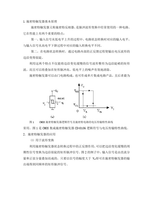
1.施密特触发器基本原理施密特触发器又称施密特反相器,是脉冲波形变换中经常使用的一种电路。
它在性能上有两个重要的特点:第一,输入信号从低电平上升的过程中,电路状态转换时对应的输入电平,与输入信号从高电平下降过程中对应的输入转换电平不同。
第二,在电路状态转换时,通过电路内部的正反馈过程使输出电压波形的边沿变得很陡。
利用这两个特点不仅能将边沿变化缓慢的信号波形整形为边沿陡峭的矩形波,而且可以将叠加在矩形脉冲高、低电平上的噪声有效地清除。
施密特触发器可以由门电路构成,也可作成单片集成电路产品,且后者最为图1 CMOS施密特触发器逻辑符号及施密特电路的电压传输特性曲线常用。
图1是CMOS集成施密特触发器CD40106逻辑符号与电压传输特性曲线。
2.施密特触发器的应用⑴用于波形变换利用施密特触发器状态转换过程中的正反馈作用,可以把边沿变化缓慢的周期性信号变换为边沿很陡的矩形脉冲信号。
图2的例子中,输入信号是由直流分量和正弦分量叠加而成的,只要以信号的幅度大于V即可在施密特触发器的输T+出端得到同频率的矩形脉冲信号。
图2 用施密特触发器实现波形变换⑵ 用于脉冲的整形在数字系统,常常需要将窄脉冲进行展宽,图3是用CD40106来展宽脉冲宽度的电路及输入、输出波形,它是利用R 、C 充电延时的作用来展宽输出脉冲的,改变R 、C 的大小,即可调节脉宽展宽的程度。
图图 3 施密特触发器实现窄脉冲展宽电路及其波形⑶ 用于单稳态触发器单稳态触发器的工作特性具有如下的显著特点:第一,它有稳态和暂稳态两个不同的工作状态;第二,在外界触发脉冲作用下,能从稳态翻转到暂稳态,在暂稳态维持一段时间以后,再自动返回稳态;V IV t (ms )t (ms )第三,暂稳态维持时间的长短取决于电路本身的参数,与触发脉冲的宽度和幅度无关。
由于具备这些特点,单稳态触发器被广泛应用于脉冲整形、延时(产生滞后于触发脉冲的输出脉冲)以及定时(产生固定时间宽度的脉冲信号)等。
SN74LVC1G14_08中文资料
FUNCTION TABLE
INPUT A
H
L
OUTPUT Y
L
H
LOGIC DIAGRAM (POSITIVE LOGIC) (DBV, DCK, DRL, DRY, and YZP Package)
A2
4Y
LOGIC DIAGRAM (POSITIVE LOGIC) (YZV Package)
A1
____ CF
CF_ C14_
CF_ CF_
(1) Package drawings, standard packing quantities, thermal data, symbolization, and PCB design guidelines are available at /sc/package.
NanoFree is a trademark of Texas Instruments.
PRODUCTION DATA information is current as of publication date. Products conform to specifications per the terms of the Texas Instruments standard warranty. Production processing does not necessarily include testing of all parameters.
– 1000-V Charged-Device Model (C101)
DCK PACKAGE (TOP VIEW)
DRL PACKAGE (TOP VIEW)
NC
1
5
VCC
NC
1
详细施密特触发器74HC14的中文资料

详细施密特触发器74HC14的中文资料74HC14为一个六反相施密特触发器真值表:Y=AInput输入output输出AYLHHL74HC14的引脚图如下,其中Vcc(14脚)是电源正电压引脚,GND(7脚)是电源地引脚,一片74HC14上共有6个反相器通道,第1、3、5、9、11、13脚分别是通道1、2、3、4、5、6的输入脚,2、4、6、8、10、12脚分别是通道1、2、3、4、5、6的输入出脚。
建议操作条件符号参数最小典型最大单位电源电压为 4.7555.25VVT,正向输入阈值电压为1.41.61.9VVT,反向输入阈值电压为0.50.81VHYS,输入滞后0.40.8-VIOHHIGH 高电平输出电流---0.4mAIOLLOW,低电平输出电流--8mATAFree ,工作温度0-70℃Note 2:VCC = 5V.电气特性超过推荐的工作自由空气温度范围(除非另有说明),符号参数条件最小典型最大单位输入钳位电压VCC 为最小,II = -18mA---1.5VVOHHIGH输出高电平电压VCC 为最小,IOH为最大VIL=最大2.73.4-VVOLLOW Level输出低电平电压VCC = 最小,IOL = 最大-0.350.5--Output V oltage输出电压VIH = 最小---VVCC = 最小,IOL = 4mA-0.250.4IT,正向阈值输入电流VCC = 5V,VI = VT+--0.14-mAIT,反向阈值输入电流VCC = 5V,VI = VT---0.18-mAII,输入电流@最大输入电压VCC = 最大,VI = 7V--0.1mAIIHHIGH ,输入高电平电流VCC = 最大,VI = 2.7V--20μAIILLOW ,输入低电平电流VCC = 最大,VI = 0.4V---0.4mAIOSShort ,短路输出电流VCC = 最大(Note 4)-20--100mAICCH,电平输出电源电流VCC = 最大-8.616mAICCL,低电平输出电源电流VCC = 最大-1221mANote 3:VCC = 5V,TA = 25℃.Note 4:一次不应超过一个输出,持续时间不应超过一秒。
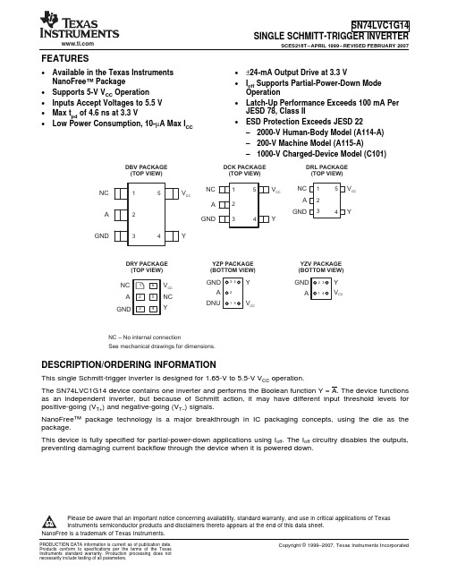
74LVC1G14单芯片阈值稳定器反转器数据表说明书

74LVC1G14Single Schmitt-trigger inverterRev. 15 — 8 June 2018Product data sheet1General descriptionThe 74LVC1G14 provides the inverting buffer function with Schmitt-trigger input. It iscapable of transforming slowly changing input signals into sharply defined, jitter-freeoutput signals.The input can be driven from either 3.3 V or 5 V devices. This feature allows the useof this device in a mixed 3.3 V and 5 V environment. Schmitt-trigger action at the inputmakes the circuit tolerant for slower input rise and fall time.This device is fully specified for partial power-down applications using I OFF. The I OFFcircuitry disables the output, preventing the damaging backflow current through thedevice when it is powered down.2Features and benefits•Wide supply voltage range from 1.65 V to 5.5 V•High noise immunity•Complies with JEDEC standard:–JESD8-7 (1.65 V to 1.95 V)–JESD8-5 (2.3 V to 2.7 V)–JESD8-B/JESD36 (2.7 V to 3.6 V).•±24 mA output drive (V CC = 3.0 V)•CMOS low power consumption•Latch-up performance exceeds 250 mA•Direct interface with TTL levels•Unlimited rise and fall times•Input accepts voltages up to 5 V•Multiple package options•ESD protection:–HBM: ANSI/ESDA/JEDEC JS-001 Class 2 exceeds 2000 V–MM: JESD22-A115-A exceeds 200 V.•Specified from -40 °C to +85 °C and -40 °C to +125 °C.3Applications•Wave and pulse shaper•Astable multivibrator•Monostable multivibratorSingle Schmitt-trigger inverter 4Ordering information5Marking[1]The pin 1 indicator is located on the lower left corner of the device, below the marking code.Single Schmitt-trigger inverter6Functional diagram7Pinning information7.1Pinning74LVC1G14n.c.V CCA GNDY001aab65512354Figure 4. Pin configuration SOT353-1 and SOT75374LVC1G14A 001aae976n.c.GNDn.c.V CC YT ransparent top view231546Figure 5. Pin configuration SOT886, SOT891, SOT1115and SOT1202n.c.V CCGND13254AY aaa-003024Transparent top view 74LVC1G14Figure 6. Pin configuration SOT1226 (X2SON5)aaa-028401Transparent top view74LVC1G14V CC4Y3A 1GND 2Figure 7. Pin configuration SOT1269-2 (X2SON4)7.2Pin descriptionSingle Schmitt-trigger inverter8Functional description[1][1]H = HIGH voltage level; L = LOW voltage level9Limiting valuesTable 5. Limiting valuesIn accordance with the Absolute Maximum Rating System (IEC 60134). Voltages are referenced to GND (ground = 0 V).[1]The input and output voltage ratings may be exceeded if the input and output current ratings are observed.[2]For TSSOP5 and SC-74A packages: above 87.5 °C the value of P tot derates linearly with 4.0 mW/K.For XSON6 and X2SON5 package: above 118 °C the value of P tot derates linearly with 7.8 mW/K.[3]For X2SON4 packages: above 57 °C the value of P tot derates linearly with 1.7 mW/K.Single Schmitt-trigger inverter 10Recommended operating conditions11Static characteristicsTable 7. Static characteristicsAt recommended operating conditions; voltages are referenced to GND (ground = 0 V).Single Schmitt-trigger inverter[1]All typical values are measured at maximum V CC and T amb = 25 °C.Table 8. Transfer characteristicsVoltages are referenced to GND (ground = 0 V); for test circuit see Figure 9.[1]Typical values are measured at T amb = 25 °C and V CC = 1.8 V, 2.5 V, 2.7 V, 3.3 V and 5.0 V respectively.Single Schmitt-trigger inverter 12Dynamic characteristicsTable 9. Dynamic characteristicsVoltages are referenced to GND (ground = 0 V); for test circuit see Figure 9.[1]Typical values are measured at T amb = 25 °C and V CC = 1.8 V, 2.5 V, 2.7 V, 3.3 V and 5.0 V respectively.[2]t pd is the same as t PLH and t PHL.[3]C PD is used to determine the dynamic power dissipation (P D in μW).P D = C PD x V CC2 x f i + (C L x V CC2 x f o) where:f i = input frequency in MHz;f o = output frequency in MHz;C L = output load capacitance in pF;V CC = supply voltage in V.12.1Waveform and test circuitSingle Schmitt-trigger inverterSingle Schmitt-trigger inverter12.2Waveforms transfer characteristics13Application informationThe slow input rise and fall times cause additional power dissipation, this can becalculated using the following formula:P add = f i x (t r x ΔI CC(AV) + t f x ΔI CC(AV)) x V CC where:•P add = additional power dissipation (μW);•f i = input frequency (MHz);•t r = input rise time (ns); 10 % to 90 %;•t f = input fall time (ns); 90 % to 10 %;•ΔI CC(AV) = average additional supply current (μA).Average ΔI CC(AV) differs with positive or negative input transitions, as shown in Figure 13.An example of a relaxation circuit using the 74LVC1G14 is shown in Figure 14.Single Schmitt-trigger inverteraaa-0219851234560.20.40.60.811.2V CC (V)KFigure 15. Typical K-factor for relaxation oscillatorSingle Schmitt-trigger inverter 14Package outlineSingle Schmitt-trigger inverterSingle Schmitt-trigger inverterSingle Schmitt-trigger inverterSingle Schmitt-trigger inverterSingle Schmitt-trigger inverterSingle Schmitt-trigger inverterSingle Schmitt-trigger inverterSingle Schmitt-trigger inverter 15Abbreviations16Revision historySingle Schmitt-trigger inverter 17Legal information17.1 Data sheet status[1]Please consult the most recently issued document before initiating or completing a design.[2]The term 'short data sheet' is explained in section "Definitions".[3]The product status of device(s) described in this document may have changed since this document was published and may differ in case of multipledevices. The latest product status information is available on the Internet at URL .17.2 DefinitionsDraft — The document is a draft version only. The content is still under internal review and subject to formal approval, which may result in modifications or additions. Nexperia does not give any representations or warranties as to the accuracy or completeness of information included herein and shall have no liability for the consequences of use of such information.Short data sheet — A short data sheet is an extract from a full data sheet with the same product type number(s) and title. A short data sheet is intended for quick reference only and should not be relied upon to contain detailed and full information. For detailed and full information see the relevant full data sheet, which is available on request via the local Nexperia sales office. In case of any inconsistency or conflict with the short data sheet, the full data sheet shall prevail.Product specification — The information and data provided in a Product data sheet shall define the specification of the product as agreed between Nexperia and its customer, unless Nexperia and customer have explicitly agreed otherwise in writing. In no event however, shall an agreement be valid in which the Nexperia product is deemed to offer functions and qualities beyond those described in the Product data sheet.17.3 DisclaimersLimited warranty and liability — Information in this document is believed to be accurate and reliable. However, Nexperia does not give any representations or warranties, expressed or implied, as to the accuracyor completeness of such information and shall have no liability for the consequences of use of such information. Nexperia takes no responsibility for the content in this document if provided by an information source outside of Nexperia. In no event shall Nexperia be liable for any indirect, incidental, punitive, special or consequential damages (including - without limitation -lost profits, lost savings, business interruption, costs related to the removal or replacement of any products or rework charges) whether or not such damages are based on tort (including negligence), warranty, breach of contract or any other legal theory. Notwithstanding any damages that customer might incur for any reason whatsoever, Nexperia's aggregate and cumulative liability towards customer for the products described herein shall be limited in accordance with the Terms and conditions of commercial sale of Nexperia.Right to make changes — Nexperia reserves the right to make changesto information published in this document, including without limitation specifications and product descriptions, at any time and without notice. This document supersedes and replaces all information supplied prior to the publication hereof.Suitability for use — Nexperia products are not designed, authorized or warranted to be suitable for use in life support, life-critical or safety-critical systems or equipment, nor in applications where failure or malfunctionof an Nexperia product can reasonably be expected to result in personal injury, death or severe property or environmental damage. Nexperia and its suppliers accept no liability for inclusion and/or use of Nexperia products in such equipment or applications and therefore such inclusion and/or use is at the customer’s own risk.Applications — Applications that are described herein for any of these products are for illustrative purposes only. Nexperia makes no representation or warranty that such applications will be suitable for the specified use without further testing or modification. Customers are responsible for the design and operation of their applications and products using Nexperia products, and Nexperia accepts no liability for any assistance with applications or customer product design. It is customer’s sole responsibility to determine whether the Nexperia product is suitable and fit for the customer’s applications and products planned, as well as for the planned application and use of customer’s third party customer(s). Customers should provide appropriate design and operating safeguards to minimize the risks associated with their applications and products. Nexperia does not accept any liability related to any default, damage, costs or problem which is based on any weakness or default in the customer’s applications or products, or the application or use by customer’s third party customer(s). Customer is responsible for doing all necessary testing for the customer’s applications and products using Nexperia products in order to avoid a default of the applications and the products or of the application or use by customer’s third party customer(s). Nexperia does not accept any liability in this respect.Limiting values — Stress above one or more limiting values (as defined in the Absolute Maximum Ratings System of IEC 60134) will cause permanent damage to the device. Limiting values are stress ratings only and (proper) operation of the device at these or any other conditions above thosegiven in the Recommended operating conditions section (if present) or the Characteristics sections of this document is not warranted. Constant or repeated exposure to limiting values will permanently and irreversibly affect the quality and reliability of the device.Terms and conditions of commercial sale — Nexperia products aresold subject to the general terms and conditions of commercial sale, as published at /profile/terms, unless otherwise agreed in a valid written individual agreement. In case an individual agreement is concluded only the terms and conditions of the respective agreement shall apply. Nexperia hereby expressly objects to applying the customer’s general terms and conditions with regard to the purchase of Nexperia products by customer.No offer to sell or license — Nothing in this document may be interpreted or construed as an offer to sell products that is open for acceptance orthe grant, conveyance or implication of any license under any copyrights, patents or other industrial or intellectual property rights.Export control — This document as well as the item(s) described herein may be subject to export control regulations. Export might require a prior authorization from competent authorities.Single Schmitt-trigger inverterNon-automotive qualified products — Unless this data sheet expressly states that this specific Nexperia product is automotive qualified, the product is not suitable for automotive use. It is neither qualified nor tested in accordance with automotive testing or application requirements. Nexperia accepts no liability for inclusion and/or use of non-automotive qualified products in automotive equipment or applications. In the event that customer uses the product for design-in and use in automotive applications to automotive specifications and standards, customer (a) shall use the product without Nexperia's warranty of the product for such automotive applications, use and specifications, and (b) whenever customer uses the product for automotive applications beyond Nexperia's specifications such use shall be solely at customer’s own risk, and (c) customer fully indemnifies Nexperia for any liability, damages or failed product claims resulting from customer design and use of the product for automotive applications beyond Nexperia's standard warranty and Nexperia's product specifications.Translations — A non-English (translated) version of a document is for reference only. The English version shall prevail in case of any discrepancy between the translated and English versions.17.4 TrademarksNotice: All referenced brands, product names, service names and trademarks are the property of their respective owners.74LVC1G14All information provided in this document is subject to legal disclaimers.© Nexperia B.V. 2018. All rights reserved. Product data sheet Rev. 15 — 8 June 201821 / 22Single Schmitt-trigger inverterContents1General description (1)2Features and benefits (1)3Applications (1)4Ordering information (2)5Marking (2)6Functional diagram (3)7Pinning information (3)7.1Pinning (3)7.2Pin description (3)8Functional description (4)9Limiting values (4)10Recommended operating conditions (5)11Static characteristics (5)12Dynamic characteristics (7)12.1Waveform and test circuit (7)12.2Waveforms transfer characteristics (9)13Application information (9)14Package outline (11)15Abbreviations (19)16Revision history (19)17Legal information (20)Please be aware that important notices concerning this document and the product(s)described herein, have been included in section 'Legal information'.© Nexperia B.V. 2018.All rights reserved.For more information, please visit: Forsalesofficeaddresses,pleasesendanemailto:***************************Date of release: 8 June 2018Document identifier: 74LVC1G14Mouser ElectronicsAuthorized DistributorClick to View Pricing, Inventory, Delivery & Lifecycle Information:N experia:74LVC1G14GS,13274LVC1G14GN,13274LVC1G14GF,13274LVC1G14GM,11574LVC1G14GM,132 74LVC1G14GV,12574LVC1G14GW,12574LVC1G14GX,12574LVC1G14GX4Z。
SN74LVC14A中文资料

• Inputs Accept Voltages to 5.5 V
• Max tpd of 6.4 ns at 3.3 V • Typical VOLP (Output Ground Bounce)
• ESD Protection Exceeds JESD 22 – 2000-V Human-Body Model (A114-A)
– 200-V Machine Model (A115-A)
– 1000-V Charged-Device Model (C101)
SN54LVC14A . . . J OR W PACKAGE SN74LVC14A . . . D, DB, DGV, NS,
Please be aware that an important notice concerning availability, standard warranty, and use in critical applications of Texas Instruments semiconductor products and disclaimers thereto appears at the end of this data sheet.
VCC
Supply voltage
VI
Input voltage
VO
Output voltage
IOH
High-level output current
IOL
Low-level output current
Operating Data retention only
施密特触发器
VOL
vI
输 VT+ VT− 入
0
VT−
VT+
vI
vO 输 vOH 出 v OL
0
t t
0
本页完 继续
施密特触发器
本内容结束页
1
vI
1
一、典型施密特触发器一 2、工作过程分析 R1 VT+= ( 1+ ) VTH R2 R VT-= ( 1− 1 ) VTH R2 3、施密特电路的传输特性
vO
vO vO
I
输 V TH 入
1.电路组成
0
t
vO vOH
输 出 v OL
0
t 本页完 继续
施密特触发器
2.工作过程分析 (1)开始时刻
二、典型施密特触发器二 1、电路组成 设输入为 电路特点:二极管和电阻R1 0V(“0”) 可使施密特触发器有一个回差 电压(或称滞后电压)VT。 2、工作过程分析 (1)开始刻vI=“0”(0V)
西藏· 阿里· 扎达土林
&
返回
封面
前言
施密特触发器不同于前述的各类触发器,
它具有下述特点:
(1)施密特触发器属于电平触发,对于缓
慢变化的信号仍然适用,当输入信号达到某
一额定值时,输出电平会发生突变。
(2)对于正向和负向增长的输入信号,电
路有不同的阈值电平,即具有滞后电压传输 特性。
返回 前言
施密特电路的作用示例1 施密特电路的作用
一、典型施密特触发器一 2、工作过程分析 R 3、此时的v1I值称为VT-。 VT+= ( 1+ ) VTH R2 此时电路引发正反馈。 1、当vI下降时,只要 vA↑→vO1↓→vO↑ vA 未下降至 VTH , 电 路 状态不变。 正反馈的结果很快令vO=1。
SN74LVC14中文资料

ORDERABLE PART NUMBER SN74LVC14ARGYR SN74LVC14AD SN74LVC14ADR SN74LVC14ADT SN74LVC14ANSR SN74LVC14ADBR SN74LVC14APW SN74LVC14APWR SN74LVC14APWT SN74LVC14ADGVR SNJ54LVC14AJ SNJ54LVC14AW SNJ54LVC14AFK
ORDERING INFORMATION
TA –40°C to 85°C
施密特触发器电路及工作原理详解
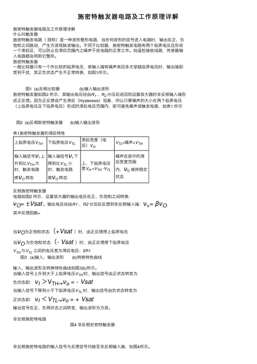
施密特触发器电路及⼯作原理详解施密特触发器电路及⼯作原理详解什么叫触发器施密特触发电路(简称)是⼀种波形整形电路,当任何波形的信号进⼊电路时,输出在正、负饱和之间跳动,产⽣⽅波或脉波输出。
不同于⽐较器,施密特触发电路有两个临界电压且形成⼀个滞后区,可以防⽌在滞后范围内之噪声⼲扰电路的正常⼯作。
如遥控接收线路,传感器输⼊电路都会⽤到它整形。
施密特触发器⼀般⽐较器只有⼀个作⽐较的临界电压,若输⼊端有噪声来回多次穿越临界电压时,输出端即受到⼲扰,其正负状态产⽣不正常转换,如图1所⽰。
图1 (a)反相⽐较器 (b)输⼊输出波形施密特触发器如图2 所⽰,其输出电压经由R1、R2分压后送回到运算放⼤器的⾮反相输⼊端形成正反馈。
因为正反馈会产⽣滞后(Hysteresis)现象,所以只要噪声的⼤⼩在两个临界电压(上临界电压及下临界电压)形成的滞后电压范围内,即可避免噪声误触发电路,如表1 所⽰图2 (a)反相斯密特触发器 (b)输⼊输出波形表1施密特触发器的滞后特性上临界电压V TH下临界电压V TL 滞后宽度(电压)V HV TL<噪声<V TH输⼊端信号νI上升到⽐V TH⼤时,触发电路使νO 转态输⼊端信号νI 下降到⽐V TL⼩时,触发电路使νO转态上、下临界电压差V H =V TH -V TL噪声在容许的滞后宽度范围内,νO维持稳定状态反相施密特触发器电路如图2 所⽰,运算放⼤器的输出电压在正、负饱和之间转换:νO= ±Vsat。
输出电压经由R1 、R2分压后反馈到⾮反相输⼊端:ν+= βνO,其中反馈因数=当νO为正饱和状态(+Vsat)时,由正反馈得上临界电压当νO为负饱和状态(- Vsat)时,由正反馈得下临界电压V TH与V TL之间的电压差为滞后电压:2R1图3 (a)输⼊、输出波形 (b)转换特性曲线输⼊、输出波形及转换特性曲线如图3(b)所⽰。
当输⼊信号上升到⼤于上临界电压V TH时,输出信号由正状态转变为负状态即:νI >V TH→νo = - Vsat当输⼊信号下降到⼩于下临界电压V TL时,输出信号由负状态转变为正状态即:νI <V TL→νo = + Vsat输出信号在正、负两状态之间转变,输出波形为⽅波。
74HC04和74HC14的区别(施密特触发的作用)

74HC04和74HC14的具体区别详解同样具有反相器功能,你知道74HC04和74HC14的具体区别吗?对于74HC04很好理解,输入低电平,输出高电平;输入高电平,输出低电平。
可是具体到几伏电压算高电平,几伏算低电平呢?答案是看手册。
下图是TI的74HC04的输入特性表,举个例子来看,当芯片供电电压Vcc=4.5V时,输入端最少输入3.15V 电压才可以被74HC04识别为高电平;同理,输入端只有输入不大于1.35V的电压,才可以被识别为低电平。
下图是74HC04的输出特性表,在TEST CONDITIONS(测试条件)分别选IOH=-4mA和IOL=4mA,再举例子看,同上面的一样,当芯片供电电压Vcc=4.5V时,且输入端被识别为低电平,输出端VOH就是高电平,且最小值为3.84V;同理,当芯片供电电压Vcc=4.5V时,且输入端被识别为高电平,输出端VOL就是低电平,且最大值为0.33V。
从以上的分析可以看出,经74HC04的反相,到底输出几伏的高电平或低电平主要和该芯片的供电电压关系密切!以上对于74HC04的分析同样适用于74HC14!关于以上的数据,他们在手册中完全一样!也就是单纯作为反相器使用时,可以通用。
但是74HC14除了反相器这个基本功能外,他还是个施密特触发器。
关于什么是施密特触发器,现用一个图简单介绍:对于74HC14来说,当输入VI大于阀值电压VT+时,输出VO由高电平变低电平;当输入VI小于阀值电压VT-时,输出VO由低电平变高电平;通过上面分析,我们了解了施密特触发器是以反相器为基础的,以及阀值电压的基本概念。
下面来看一下74HC14这个施密特触发器的手册数据:VOH和VOL上文已经介绍过了,下面看一下VT+和VT-:当芯片供电电压Vcc=4.5V时,正向阀值的典型值VT+=2.5V,负向阀值的典型值VT-=1.6V。
也就说,当输入大于2.5V时,输出为低电平;当输入小于1.6V时,输出为高电平。
施密特触发器
施密特触发器编辑词条施密特触发器也有两个稳定状态,但与一般触发器不同的是,施密特触发器采用电位触发方式,其状态由输入信号电位维持;对于负向递减和正向递增两种不同变化方向的输入信号,施密特触发器有不同的阀值电压简介折叠编辑本段门电路有一个阈值电压,当输入电压从低电平上升到阈值电压或从高电平下降到阈值电压时电路的状态将发生变化。
施密特触发器是一种特殊的门电路,与普通的门电路不同,施密特触发器有两个阈值电压,分别称为正向阈值电压和负向阈值电压。
在输入信号从低电平上升到高电平的过程中使电路状态发生变化的输入电压称为正向阈值电压,在输入信号从高电平下降到低电平的过程中使电路状态发生变化的输入电压称为负向阈值电压。
正向阈值电压与负向阈值电压之差称为回差电压。
它是一种阈值开关电路,具有突变输入——输出特性的门电路。
这种电路被设计成阻止输入电压出现微小变化(低于某一阈值)而引起的输出电压的改变。
利用施密特触发器状态转换过程中的正反馈作用,可以把边沿变化缓慢的周期性信号变换为边沿很陡的矩形脉冲信号。
输入的信号只要幅度大于vt+,即可在施密特触发器的输出端得到同等频率的矩形脉冲信号。
当输入电压由低向高增加,到达V+时,输出电压发生突变,而输入电压Vi由高变低,到达V-,输出电压发生突变,因而出现输出电压变化滞后的现象,可以看出对于要求一定延迟启动的电路,它是特别适用的.从传感器得到的矩形脉冲经传输后往往发生波形畸变。
当传输线上的电容较大时,波形的上升沿将明显变坏;当传输线较长,而且接受端的阻抗与传输线的阻抗不匹配时,在波形的上升沿和下降沿将产生振荡现象;当其他脉冲信号通过导线间的分布电容或公共电源线叠加到矩形脉冲信号时,信号上将出现附加的噪声。
无论出现上述的那一种情况,都可以通过用施密特反相触发器整形而得到比较理想的矩形脉冲波形。
只要施密特触发器的vt+和vt-设置得合适,均能收到满意的整形效果。
发明折叠编辑本段施密特触发器是由美国科学家奥托·赫伯特·施密特(Otto Herbert Schmitt)于1934年发明,当时他只是一个研究生,后于1937年他在其博士论文中将这一发明描述为“热电子触发器”(thermionic trigger)。
74LVC1G14
74LVC1G14
All information provided in this document is subject to legal disclaimers.
© NXP B.V. 2012. All rights reserved.
Product data sheet
Rev. 12 — 6 August 2012
Conditions
[1]
Min 0.5 0.5 0.5 0.5 50 100 65
Max +6.5 +6.5 VCC + 0.5 +6.5 50 50 +100 +150 250
Unit V V V V mA mA mA mA mA C mW
Active mode Power-down mode VI < 0 V VO > VCC or VO < 0 V VO = 0 V to VCC
74LVC1G14 74LVC1G14
n.c. 1 3 GND A 2 4
aaa-003024
5
VCC
n.c. A GND
1 2 3
6 5 4
VCC n.c. Y
Y
001aae976
Transparent top view
Transparent top view
Fig 6.
Pin configuration SOT891, SOT1115 and SOT1202
Table 1. Ordering information Package Temperature range 74LVC1G14GW 74LVC1G14GV 74LVC1G14GM 74LVC1G14GF 74LVC1G14GN 74LVC1G14GS 74LVC1G14GX 40 C to +125 C 40 C to +125 C 40 C to +125 C 40 C to +125 C 40 C to +125 C 40 C to +125 C 40 C to +125 C Name TSSOP5 SC-74A XSON6 XSON6 XSON6 XSON6 X2SON5 Description plastic thin shrink small outline package; 5 leads; body width 1.25 mm plastic surface-mounted package; 5 leads Version SOT353-1 SOT753 Type number
频率特性测试仪的设计

频率特性测试仪的设计国成哲;王中训;王文奇;张珉;娄阳【摘要】To measure the frequency characteristic of the linear time-invariant system,we proposed a design of a low cost FCI for university students.This instrument is based on FPGA and high-speed ADC/DAC system.It uses DDS to generate the sine wave sweep signal.Transformed by the DAC,it is output to the measured network.Then the response of the measured network is acquired by the ADC and sent to FPGA.The FPGA measures the changes of the amplitude and the phase of the signal and sends the results to PC to display.The instrument has a frequency range of 0~20 MHz,an input gain of ±40 dB,a phase resolution of 5°,and can display the amplitude-frequency curve and the phase-frequency curve in real-time.The results can be saved as files.The design is low cost,easy to implement and strongly scalable,and can meet the needs of the target population well.%为了对线性时不变系统进行频率特性进行测试,本设计提出了一种低成本、面向学生的频率特性测试仪的设计方案,本仪器为基于FPGA及高速ADC/DAC构建的数字频率特性测试仪系统.其通过DDS产生正弦扫频信号,经高速DAC转换输出,被测网络响应信号由ADC采集后输入FPGA,得出信号经被测网络后产生的幅度变化和相位变化.本仪器具有0~20 MHz的扫频范围、±40 dB输入增益范围、5°相位分辨率、可实时显示被测网络的幅频特性曲线和相频特性曲线,并可将测试结果保存为文件.本设计成本低、易实现、具有较强的可扩展性,可很好地满足目标人群的要求.【期刊名称】《电子设计工程》【年(卷),期】2017(025)011【总页数】6页(P102-106,110)【关键词】频率特性测试仪;现场可编程逻辑阵列;信号生成;信号采集【作者】国成哲;王中训;王文奇;张珉;娄阳【作者单位】烟台大学光电信息科学与技术学院,山东烟台264005;烟台大学光电信息科学与技术学院,山东烟台264005;烟台大学光电信息科学与技术学院,山东烟台264005;烟台大学光电信息科学与技术学院,山东烟台264005;烟台大学光电信息科学与技术学院,山东烟台264005【正文语种】中文【中图分类】TN911.22频率特性是以频率为变量描述系统特性的一种图示方法。
74ls14d能否用74ls14n代替
74ls14d能否用74ls14n代替74ls14d能否用74ls14n代替74ls14d和74ls14n都是六反相施密特触发器,引脚排列一样,封装不一样。
74ls14d时贴片式封装,74ls14n是双列直插塑封。
74ls14n的体积要比74ls14d大很多,是不能直接插上的,如果你用细线焊好然后连线上,也是可以的。
也有标准74ls14d的D封装是玻璃-金属双列直插封装,要是双列直插就可替换。
在实际应用以及DXP作图上,74LS14D能否用SN74HC14N代替74LS14是TTL的,74HC14是CMOS的,可以用TTL驱动CMOS的,但反过来就不能直接用了。
看你的使用场合了,TTL的低电平和高电平的门限值很宽。
一般自己DIY的都可以直接用的。
你看下晶片资料就行了datasheet5.将高电平变低电频用74ls14n,74ls14n要接电源吗这是非闸电路,晶片工作当然要接电源,一般为5V74ls151能代替74ls298吗74LS151是8选1资料选择器.74LS298是4位2选1资料选择器.电路功能不一样,不能代替使用。
74ls244能否代替74LS245?完全代替是不行的,看你想实现什么功能咯。
244和245的PDF 里说明了,245可以用enable和dir控制所有3态门,而244分别用2个非门控制3个3态门。
245需要enable和dir同时开启才能工作,而244只需一边的非门工作其他3个3态门就工作如何用SN74LS245N代替74LS245SN74LS245N 是美国TEXAS公司的产品,尾号为N,封装是双列直插塑封。
74LS245未标公司名和封装。
两种晶片功能相同,你的74LS245的封装要是双列直插的,你直接用SN74LS245N替换就行了。
74ls148N和74LS148D的n和d代表什么?逻辑上没有差别。
N和D的差别主要指晶片封装材料的差别,N指标准塑料封装,D指塑料小外形封装。
施密特触发器的作用(共10篇)

施密特触发器的作用(共10篇)施密特触发器的作用(一): 施密特触发器的作用施密特触发器有一个门限电压,一般用做脉冲边缘不陡的整形和正弦波脉冲波发生器.施密特触发器的作用(二): 施密特触发器有什么具体作用1.波形变换可将三角波、正弦波等变成矩形波.2.脉冲波的整形数字系统中,矩形脉冲在传输中经常发生波形畸变,出现上升沿和下降沿不理想的情况,可用施密特触发器整形后,获得较理想的矩形脉冲.3.脉冲鉴幅幅度不同、不规则的脉冲信号施加到施密特触发器的输入端时,能选择幅度大于欲设值的脉冲信号进行输出.【施密特触发器的作用】施密特触发器的作用(三): 什么是施密特触发器施密特触发器,与其说是“触发器”,不如说是具有滞后特性的数字传输门.其特点有二详细图解施密特触发器的作用(四): 施密特结构有哪些作用和优点施密特触发器的应用较广,有以下几个典型应用:1、波形变换:将非矩形如正弦波波变换为矩形波.2、波形的整形与抗干扰:在传输线上电容较大时或传输线较长时,波形产生畸变,可采用施密特触发器选择恰当的回差电压对波形...施密特触发器的作用(五): 施密特触发器是具有特殊功能的非门,当加在它的输入端A的电压逐渐上升到某个值时,输出端Y会突然从高电平跳到低电平,而当输入端A的电压下降到另一个值时,Y会从低电平跳到高电平.如图是温度报警器电路示意图,RT是半导体热敏电阻,温度升高时电阻减少,下列分析正确的是()A. 升高温度时,A端电势降低;升高到某一温度时,Y端电势升高,蜂鸣器会发出报警声B. 升高温度时,A端电势升高;升高到某一温度时,Y端电势降低,蜂鸣器会发出报警声C. 增大R1时,A端电势降低;增大到某一值时,Y端势升高,蜂鸣器会发出报警声D. 增大R1时,A端电势升高;增大到某一值时,Y端势降低,蜂鸣器不会发出报警声A、B、根据电路图知,当RT的温度升高时,RT 减小,A端电势升高,经非门后,Y端电势降低,蜂鸣器会发出报警,故A错误B正确;C、D、当增大R1时,A端电势升高,经非门后,Y端电势降低,蜂鸣器会发出报警声,故CD错误;故选:B.施密特触发器的作用(六): 施密特触发器是具有特殊功能的非门,当加在它的输入端A的电压逐渐上升到某个值时,输出端Y会突然从高电平跳到低电平,而当输入端A的电压下降到另一个值时,Y会从低电平跳到高电平.如图是温度报警器电路示意图,RT是半导体热敏电阻,温度升高时电阻减少,下列分析正确的是()A.升高温度时,A端电势降低;升高到某一温度时,Y端电势升高,蜂鸣器会发出报警声B.升高温度时,A端电势升高;升高到某一温度时,Y端电势降低,蜂鸣器会发出报警声C.增大R1时,A端电势降低;增大到某一值时,Y端势升高,蜂鸣器会发出报警声D.增大R1时,A端电势升高;增大到某一值时,Y端势降低,蜂鸣器不会发出报警声A、B、根据电路图知,当RT的温度升高时,RT 减小,A端电势升高,经非门后,Y端电势降低,蜂鸣器会发出报警,故A错误B正确;C、D、当增大R1时,A端电势升高,经非门后,Y端电势降低,蜂鸣器会发出报警声,故CD错误;故选:B.施密特触发器的作用(七): 施密特触发器属于与非门吗不属于施密特触发器的作用(八): 什么是斯密特触发器怎么应用在脉冲数字信号传递过程中,要求有较好的上升沿和下降沿.施密特触发器,其特点是有滞后效应,有阈值.即当输入信号超过上限鉴别阈值VT+时,电路翻转.当输入电平回到VT+时,电路并不重新翻回,而必须在输入电平继续下降到低于VT+的另一个阈值VT-时,电路才能翻回到原来初始状态.应用有现成的集成电路,如CD40106,7414,74HC14等你用就可以了.你也可以用比较器自己设计成施密特触发器.施密特触发器的作用(九): 555定时器接成单稳态触发器,多谐振荡器,施密特触发器的电路图及输入输出波形图,单稳态触发器脉宽的计算公式,多谐振荡器周期和占空比的计算555 的周期可以通过调节输入电流大小改变的通过对2,6;7针输入电流的微小调节可是实现输出频率的调节实验六 555定时器及其应用一.实验目的1.施密特触发器的作用(十): 1、对于JK触发器,输入J=0,K=1,CLK脉冲作用后,触发器的次态应为().A:0 B:1 C:Qn D:不确定2、图2所示器件是什么类型的集成计数器().A:同步二进制加法 B:异步二进制减法 C:同步十进制加法 D:异步十进制加法 3、可以明显改善输出波形边沿的电路是().A:多谐振荡器 B:施密特触发器 C:单稳态触发器 D:定时器4、下列说法不正确的是().A:时序电路与组合电路具有不同的特点,因此其分析方法和设计方法也不同B:时序电路任意时刻的状态和输出均可表示为输入变量和电路原来状态的逻辑函数 C:用包含输出与输入逻辑关系的函数式不可以完整地描述时序电路的逻辑功能 D:用包含输出与输入逻辑关系的函数式可以完整地描述时序电路的逻辑功能5、有一个或非门构成的RS触发器,欲使该触发器保持原态,则输入信号应为(). A:S=R=0 B:S=R=1 C:S=1,R=0 D:S=0,R=16、在555定时器组成的三种电路中,能自动产生周期为T=0.7(R1+2R2)C的脉冲信号的电路是().A、多谐振荡器;B、单稳态触发器;C、施密特触发器;D、双稳态触发器1、对于JK触发器,输入J=0,K=1,CLK脉冲作用后,触发器的次态应为( a). A:0 B:1 C: QnD:不确定2、图2所示器件是什么类型的集成计数器(无图).A:同步二进制加法 B:异步二进制减法 C:同步十进制加法 D:异步十进制加法3、可以明显改善输出波形边沿的电路是( B ).A:多谐振荡器 B:施密特触发器 C:单稳态触发器 D:定时器4、下列说法不正确的是( D ).A:时序电路与组合电路具有不同的特点,因此其分析方法和设计方法也不同B:时序电路任意时刻的状态和输出均可表示为输入变量和电路原来状态的逻辑函数 C:用包含输出与输入逻辑关系的函数式不可以完整地描述时序电路的逻辑功能D:用包含输出与输入逻辑关系的函数式可以完整地描述时序电路的逻辑功能 5、有一个或非门构成的RS触发器,欲使该触发器保持原态,则输入信号应为( a ). A:S=R=0 B:S=R=1C:S=1,R=0 D:S=0,R=16、在555定时器组成的三种电路中,能自动产生周期为T=0.7(R1+2R2)C的脉冲信号的电路是( a ).A、多谐振荡器;B、单稳态触发器;C、施密特触发器;D、双稳态触发器施密特触发器施密特触发器原理。
施密特触发器 门电路符号
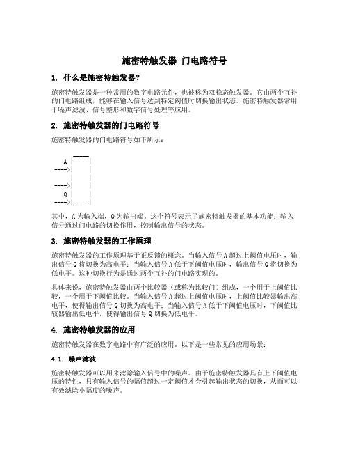
施密特触发器门电路符号1. 什么是施密特触发器?施密特触发器是一种常用的数字电路元件,也被称为双稳态触发器。
它由两个互补的门电路组成,能够在输入信号达到特定阈值时切换输出状态。
施密特触发器常用于噪声滤波、信号整形和数字信号处理等应用。
2. 施密特触发器的门电路符号施密特触发器的门电路符号如下所示:_____A | |---->| || |---->| |Q | |---->|_____|其中,A为输入端,Q为输出端。
这个符号表示了施密特触发器的基本功能:输入信号通过门电路的切换作用,控制输出信号的状态。
3. 施密特触发器的工作原理施密特触发器的工作原理基于正反馈的概念。
当输入信号A超过上阈值电压时,输出信号Q将切换为高电平;当输入信号A低于下阈值电压时,输出信号Q将切换为低电平。
这种切换行为是通过两个互补的门电路实现的。
具体来说,施密特触发器由两个比较器(或称为比较门)组成,一个用于上阈值比较,一个用于下阈值比较。
当输入信号A超过上阈值电压时,上阈值比较器输出高电平,使得输出信号Q切换为高电平;当输入信号A低于下阈值电压时,下阈值比较器输出低电平,使得输出信号Q切换为低电平。
4. 施密特触发器的应用施密特触发器在数字电路中有广泛的应用。
以下是一些常见的应用场景:4.1. 噪声滤波施密特触发器可以用来滤除输入信号中的噪声。
由于施密特触发器具有上下阈值电压的特性,只有输入信号的幅值超过一定阈值才会引起输出状态的切换,从而可以有效滤除小幅度的噪声。
4.2. 信号整形施密特触发器可以将输入信号整形为方波信号。
通过适当设置上下阈值电压,可以实现对输入信号的幅值和频率进行调整,使得输出信号更符合特定的需求。
4.3. 数字信号处理施密特触发器可以用于数字信号处理中的触发器设计。
在数字系统中,触发器常用于存储和传输数据。
施密特触发器的双稳态特性使得它非常适合用作触发器元件,能够稳定地存储和传输数字信号。
- 1、下载文档前请自行甄别文档内容的完整性,平台不提供额外的编辑、内容补充、找答案等附加服务。
- 2、"仅部分预览"的文档,不可在线预览部分如存在完整性等问题,可反馈申请退款(可完整预览的文档不适用该条件!)。
- 3、如文档侵犯您的权益,请联系客服反馈,我们会尽快为您处理(人工客服工作时间:9:00-18:30)。
1
Please be aware that an important notice concerning availability, standard warranty, and use in critical applications of Texas Instruments semiconductor products and disclaimers thereto appears at the end of this data sheet. NanoStar, NanoFree are trademarks of Texas Instruments.
over operating free-air temperature range (unless otherwise noted)
MIN
MAX UNIT
VCC Supply voltage range VI Input voltage range(2) VO Voltage range applied to any output in the high-impedance or power-off state(2) VO Voltage range applied to any output in the high or low state(2) (3)
IIK Input clamp current
VI < 0
IOK Output clamp current
VO < 0
IO Continuous output current
Continuous current through VCC or GND
DBV package
–0.5
6.5 V
–0.5
6.5 V
SN74LVC1G14
SCES647A – SEPTEMBER 2005 – REVISED JUNE 2011
SINGLE SCHMITT-TRIGGER INVERTER
Check for Samples: SN74LVC1G14
FEATURES
1
•2 Available in the Texas Instruments NanoStar™ and NanoFree™ Packages
FUNCTION TABLE
INPUT A
OUTPUT Y
H
L
L
H
LOGIC DIAGRAM (POSITIVE LOGIC) (DBV, DCK, DRL, DSF, DRY, and YZP Package)
A2
4Y
LOGIC DIAGRAM (POSITIVE LOGIC) (YZV Package)
–0.5
6.5 V
–0.5 VCC + 0.5
V
–50 mA
–50 mA
±50 mA
±100 mA
206
DCK package
252
θJA Package thermal impedance(4)
DRL package DRY package DSF package
142 234 °C/W 300
YZP package
NanoStar™ and NanoFree™ package technology is a major breakthrough in IC packaging concepts, using the die as the package.
This device is fully specified for partial-power-down applications using Ioff. The Ioff circuitry disables the outputs, preventing damaging current backflow through the device when it is powered down.
GND 3 4 Y
YZP PACKAGE (BOTTOM VIEW) GND 3 4 Y
A2 DNU 1 5 VCC
DNU − Do not use
YZV PACKAGE (BOTTOM VIEW)
GND 2 3 Y A 1 4 VCC
DSF PACKAGE (TOP VIEW)
NC 1 6 VCC A 2 5 NC
Reel of 3000
SN74LVC1G14YZVR
____ CF
SOT (SOT-23) – DBV
Reel of 3000 Reel of 250
SN74LVC1G14DBVR SN74LVC1G14DBVT
C14_
SOT (SC-70) – DCK
Reel of 3000 SN74LVC1G14DCKR
• Ioff Supports Live Insertion, Partial Power Down Mode, and Back Drive Protection
• Latch-Up Performance Exceeds 100 mA Per JESD 78, Class II
• ESD Protection Exceeds JESD 22 – 2000-V Human-Body Model (A114-A) – 200-V Machine Model (A115-A) – 1000-V Charged-Device Model (C101)
CF
(1) Package drawings, standard packing quantities, thermal data, symbolization, and PCB design guidelines are available at /sc/package.
(2) DBV/DCK/DRL/DRY: The actual top-side marking has one additional character that designates the assembly/test site. YZP: The actual top-side marking has three preceding characters to denote year, month, and sequence code, and one following character to designate the assembly/test site. Pin 1 identifier indicates solder-bump composition (1 = SnPb, • = Pb-free). YZV: The actual top-side marking is on two lines. Line 1 has four characters to denote year, month, day, and assembly/test site. Line 2 has two characters which show the family and function code. Pin 1 identifier indicates solder-bump composition (1 = SnPb, • = Pb-free).
DBV PACKAGE (TOP VIEW)
DCK PACKAGE (TOP VIEW)
DRL PACKAGE (TOP VIEW)
NC
1
A
2
5
VCC
NC
1
5
VCC
NC 1
5
GND 3 4 Y
GND
3
4
Y
DRY PACKAGE (TOP VIEW)
NC 1 6 VCC A 2 5 NC
2
PRODUCTION DATA information is current as of publication date. Products conform to specifications per the terms of the Texas Instruments standard warranty. Production processing does not necessarily include testing of all parameters.
GND 3 4 Y
NC − No internal connection
See mechanical drawings for dimensions.
DESCRIPTION/ORDERING INFORMATION
This single Schmitt-trigger inverter is designed for 1.65-V to 5.5-V VCC operation.
• Supports 5-V VCC Operation • Inputs Accept Voltages to 5.5 V
• Max tpd of 4.6 ns at 3.3 V • Low Power Consumption, 10-μA Max ICC • ±24-mA Output Drive at 3.3 V
PACKAGE (1)
ORDERABLE PART NUMBER TOP-SIDE MARKING(2)
NanoFree™ – WCSP (DSBGA) 0.23-mm Large Bump – YZP (Pb-free)
Reel of 3000
SN74LVC1G14YZPR
_ _ _CF_
NanoFree™ – WCSP (DSBGA) 0.23-mm Large Bump – YZV (Pb-free)
Copyright © 2005–2011, Texas Instruments Incorporated
SN74LVC1G14