电力电子与高频磁技术
电力电子技术在电力系统中发展重要性及应用

电力电子技术在电力系统中发展重要性及应用摘要:电力电子技术作为电工技术中的一门新技术,它融合了电力与电子技术,是新能源发电的关键性技术,它与新能源发电技术的开发利用及人们的生活水平息息相关。
近年来,随着科技水平的不断提高,出现了许多新的结构器件和材料,这些器件和材料被广泛应用于各行各业中,这为电力电子技术在电力系统中的应用拓展了空间,同时也促进了电力电子技术的发展。
就目前情况而言,电力电子技术在电力系统中的应用主要包括在发电环节中的应用、输电环节中的应用、配电环节中的应用和节能环节中的应用等,下面我们对此进行详细的探讨关键词:电力;电子技术;发展;重要性;具体应用1电力电子技术的发展电力电子技术兴起于上世纪五十年代末,从其发展历程的先后来看,可以分为整流器时代、逆变器时代和变频器时代。
而从其发展方向来看,传统的电力电子技术是以低频技术为主,而现代的电力电子技术则是以高频技术为主处理问题的。
发展方向的转变也使得电力电子技术被广泛地应用于新能源开发、电能控制等等领域。
上世纪八十年代,柔性交流输电技术的出现和电力设备多样化的开展进展极大地促进了电力系统的发展,但是相比欧美、日本等发达国家,由于起步较晚,我国的电力电子技术还是存在明显差距的。
因此,我国电力电子技术的开发依然任重而道远,要想真正地实现自主研发,除了踏实认真地学习发达国家的技术外,我们更应该注重创新,提高创新意识。
2电力电子技术在电力系统中的重要性电力电子技术不仅包含了传统技术的长处,还以实际情况为基础进行了合理的调整,对于电力系统来说它的重要性也越来越高。
首先,电力电子技术能够合理利用并优化配置电力系统的相关资源,做到对电能的优化使用。
其次,通过改造传统产业电力电子技术实现了新型机电一体化的目标,为电力系统的良好运行提供了保障。
除此之外,机电设备在电力电子技术的支持下走向了高频化与变频化。
最后,因为电力电子技术的发展,电力系统变得越发智能化。
电力电子技术
电力电子技术当今社会的发展离不开电力电子技术的支持。
电力电子技术是指将电力电子器件和电力电路拓扑应用到电力领域中的技术,主要应用于电力变换、电力传输、电力质量控制和电能利用等领域。
本文将介绍电力电子技术的基础原理、应用及发展趋势。
一、电力电子技术的基础原理电力电子技术的基础是电力电子器件。
电力电子器件指的是能够控制电能流动的器件,包括二极管、晶闸管、可控硅、绝缘栅双极性晶体管(IGBT)和金属氧化物半导体场效应晶体管(MOSFET)等。
这些器件的特点在于其能够实现对电源电压、电流、频率、相位等参数的控制,从而实现电力电子产品的精准控制和调节。
电力电子器件的基本工作原理是控制电压和电流的方向和大小。
比如,晶闸管通过改变电压斩波角的方式,控制电流通过电路的情况;可控硅则通过控制正半周的电压斩波角和反半周的通导角度来控制电流通过电路的情况;IGBT则通过控制集电极电流和栅电极电压的方式,控制集电极电压和电流的大小。
二、电力电子技术的应用电力电子技术的应用越来越广泛,其主要应用领域包括以下几个方面:1、电力传输和变换在电力传输和变换中,电力电子技术能够实现变压器的比例变换、功率因数控制,减小电路开关的能量损耗,从而达到提高效率、控制电流、保护系统的目的。
常见的应用包括变频调速、变压器、稳压电源等。
2、电力控制电力电子技术可以实现电力控制,如调节电压、电机控制、电池充放电控制等。
电力电子技术还可以实现提高功率计量的准确性和反映电力质量的指标,如电流谐波、功率因数等。
3、新能源应用随着新能源的广泛应用,电力电子技术在太阳能、风能等新能源领域也有了广泛应用。
例如,太阳能光电池的控制可以用到电力电子技术,能够实现太阳能光电池的效率和输出电压的调节。
4、电力质量控制电力电子技术可以帮助实现电力传输过程中的质量控制。
例如,电力电子技术可以帮助实现通过控制谐波电流降低电网电流的谐波污染;通过控制谐波电压稳定电网的电压。
电力电子设备电磁兼容性设计

电力电子设备电磁兼容性设计引言随着电力电子技术的发展,电力电子设备在能源转换、传输和分配中起着至关重要的作用。
然而,由于电力电子设备中的高频电磁干扰,导致电磁兼容性问题成为一个日益严重的挑战。
本文将探讨电力电子设备的电磁兼容性问题,并介绍一些设计原则和方法来提高电力电子设备的电磁兼容性。
电磁干扰的原因和影响电力电子设备产生的高频电磁干扰主要由以下几个方面造成:1.开关干扰:电力电子设备中的开关元件(如晶体管、二极管)会产生大量高频开关干扰信号,这些信号会传播到设备的其他部分和周围环境中。
2.电源干扰:电力电子设备中的电源回路会产生高频电磁干扰,主要是由于电源输入和输出之间的电容和电感。
3.高频回路干扰:电力电子设备中的高频电路(如滤波电路、谐振电路)会产生高频电磁干扰信号,这些信号会辐射到设备的其他部分和周围环境中。
这些高频电磁干扰信号会对电力电子设备自身产生以下影响:1.性能降低:高频电磁干扰信号会干扰设备正常的工作信号,导致设备性能下降,甚至出现故障。
2.其他设备的干扰:设备辐射的高频电磁干扰信号可能干扰周围的其他电子设备,引起干扰或故障。
3.对人体健康的影响:高频电磁辐射可能对人体健康产生不良影响,如头痛、失眠等。
为了解决这些问题,电力电子设备的电磁兼容性设计变得至关重要。
电磁兼容性设计原则和方法为了提高电力电子设备的电磁兼容性,可以采取以下原则和方法:1. 布局和屏蔽合理的设备布局和屏蔽设计可以降低电磁干扰的传播和辐射。
具体措施包括:•分层布局:将不同功能的电路板分层放置,减少彼此之间的干扰。
•高频信号屏蔽:使用金属屏蔽罩、屏蔽壳等,对高频信号进行屏蔽,阻止其辐射到其他部分。
•地面屏蔽:加强设备的地面屏蔽,减少地面回路干扰。
2. 滤波器设计合理设计滤波器可以减少电力电子设备辐射的高频电磁干扰信号。
滤波器可以包括输入滤波器和输出滤波器。
具体措施包括:•输入滤波器:通过合理设计输入滤波器,可以降低电源干扰信号的传导。
电力电子技术的未来发展趋势是什么?
电力电子技术的未来发展趋势是什么?在当今科技飞速发展的时代,电力电子技术作为一门关键的交叉学科,正以前所未有的速度改变着我们的生活和工业生产方式。
从智能手机的快速充电到电动汽车的高效驱动,从可再生能源的大规模并网到智能电网的优化运行,电力电子技术的身影无处不在。
那么,未来电力电子技术又将朝着哪些方向发展呢?首先,更高的功率密度和效率将是电力电子技术追求的重要目标。
随着电子设备的日益小型化和功能的不断强大,对电源模块的功率密度提出了越来越高的要求。
通过采用新型的半导体材料,如碳化硅(SiC)和氮化镓(GaN),以及优化电路拓扑结构和控制策略,可以显著提高电力电子装置的功率密度和效率。
这不仅能够减少设备的体积和重量,还能降低能源消耗,为实现可持续发展做出贡献。
在半导体技术方面,宽禁带半导体器件的发展将成为未来的主流趋势。
相较于传统的硅基半导体器件,SiC 和 GaN 具有更高的击穿电场强度、更高的热导率和更低的导通电阻。
这使得它们能够在更高的电压、温度和频率下工作,从而提高电力电子系统的性能。
例如,在电动汽车的充电器中,采用 SiC 器件可以大大缩短充电时间,提高充电效率;在光伏逆变器中,使用 GaN 器件能够降低能量损耗,增加发电量。
集成化也是电力电子技术未来发展的一个重要方向。
将多个功能模块集成在一个芯片上,可以减少寄生参数,提高系统的可靠性和稳定性。
此外,系统级封装(SiP)和三维封装技术的不断进步,将为电力电子集成化提供更多的可能性。
未来,我们可能会看到更多高度集成的电力电子模块,它们不仅具有功率变换功能,还集成了驱动、控制和保护等电路,从而简化系统设计,降低成本。
智能化控制技术将在电力电子领域发挥越来越重要的作用。
随着人工智能、大数据和机器学习的发展,电力电子系统可以实现更加精确和自适应的控制。
通过对系统运行数据的实时监测和分析,智能控制器能够根据负载变化和工作环境的动态调整控制策略,以达到最优的性能。
电力电子技术的发展趋势及应用
电力电子技术的发展趋势及应用半导体的出现成为20世纪现代物理学的一项最重大的突破,标志着电子技术的诞生。
而由于不同领域的实际需要,促使半导体器件自此分别向两个分支快速发展,其中一个分支即是以集成电路为代表的微电子器件,而另一类就是电力电子器件,特点是功率大、快速化。
自20世纪五十年代末第一只晶闸管问世以来,电力电子技术开始登上现代电气传动技术舞台,以此为基础开发的可控硅整流装置,是电气传动领域的一次革命,使电能的变换和控制从旋转变流机组和静止离子变流器进入由电力电子器件构成的变流器时代,这标志着电力电子的诞生。
电子电力技术包括电力电子器件、变流电路和控制电路3部分,是以电力为处理对象并集电力、电子、控制三大电气工程技术领域之间的综合性学科。
电力技术涉及发电、输电、配电及电力应用,电子技术涉及电子器件和由各种电子电路所组成的电子设备和系统,控制技术是指利用外加的设备或装置使机器设备或生产过程的某个工作状态或参数按照预定的规律运行。
电力电子器件是电力电子技术的基础,电力电子器件对电能进行控制和转换就是电子电力技术的利用。
在21世纪已经成为一种高新技术,影响着人们生活的各种领域,因此对对电子电力技术的研究具有时代意义。
传统电力电子技术是以低频技术处理的,现代电力电子的发展向着高频技术处理发展。
其发展先后经历了整流器时代、逆变器时代和变频器时代,在不断的发展中促进了现代电力电子技术的广泛应用。
电力电子技术在1947年晶体管诞生开始形成,接着1956的晶闸管的出现标志电力电子技术逐渐形成一门学科开始发展,以功率MOS-FET和IGBT为代表的、集高频、高压和大电流于一身的功率半导体复合器件的出现,表明已经进入现代电子电力技术发展时代。
1.整流器时代在60年代到70年代被称为电力电子技术的整流时代。
该期间主要是大功率硅整流管和晶闸管的开发与应用。
1948年的晶体管的出现引发了电子工业革命,半导体器件开始应用与通信领域,1957年,晶闸管的诞生扩展了半导体器件功率控制范围,属于第一代电力电子器件。
电力电子技术中的电磁兼容性设计

电力电子技术中的电磁兼容性设计电磁兼容性设计是电力电子技术中必须关注的一个重要方面。
电力电子设备需要在分布式电源、智能电网、清洁能源和高速列车等应用场景中发挥作用,因此在这些应用场景中需要高度注意电磁兼容性的问题。
在本文中,我们将讨论电力电子技术中的电磁兼容性设计。
1. 什么是电磁兼容性?在我们开始讨论电力电子技术中的电磁兼容性设计之前,让我们首先了解一下什么是电磁兼容性。
电磁兼容性通常是指电子设备在电磁环境中与其他设备、系统或环境进行协调、共存甚至共生存的能力。
简而言之,电磁兼容性是一种能够确保电子设备能正常运行且在电磁环境中不产生外部干扰或承受来自外部的干扰的能力。
2. 电力电子技术中的电磁兼容性电力电子技术中的电磁兼容性设计是确保电力电子设备能够在电磁环境中工作并保持高效性的重要一环。
因为电力电子设备通常在高功率状态下运行,为了确保其不受来自其他设备的干扰以及不会对其他设备或环境造成干扰,必须从设备选型、设计、制造和安装等方面考虑电磁兼容性。
3. 电磁干扰的来源电磁干扰的来源是多方面的,它可以来自电力电子设备自身,也可以来自其他设备或环境。
在电力电子技术中,电磁干扰主要来自以下几个方面:(1) 电源/信号线。
电源和信号线是交流电功率/信号输入和输出的主要途径。
这些线路可以作为天线,发射和接收电磁波信号。
(2) 开关元件。
开关元件的开关动作会产生大量噪声和高频随机变化,从而产生电磁干扰。
(3) 电磁辐射。
所有的电子设备都会产生电磁辐射。
尤其是在高压和高功率设备中,电磁辐射可能会对周围的设备和人产生影响。
4. 电磁兼容性设计的方法电磁兼容性设计是为了确保电力电子设备可以在电磁环境中正常工作而采用的一系列方法和手段。
这些方法和手段包括:(1) 策略性地选择设备。
在电力电子设备设计的起始阶段,选择高品质的设备是非常重要的。
例如,低噪声、低漏磁等特性的元器件可以降低设备的电磁辐射和电磁信噪比。
(2) 开展电磁兼容性分析。
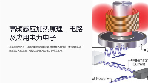
高频感应加热原理、电路及应用电力电子
电力电子的发展趋势
可再生能源
随着可再生能源的快速发展,电 力电子技术在太阳能、风能等领 域的应用日益广泛。
电动汽车
电力电子技术在电动汽车中发挥 关键作用,推动交通领域向清洁 能源转型。
智能电网
电力电子技术在智能电网中的应 用,可以实现能源的高效利用和 智能管理。
电力电子的应用领域ຫໍສະໝຸດ 1电力调节2
对电能进行调节和控制,保证电力系统
的稳定运行。
3
能源转换
将电能转换为其他形式的能量,如电机 驱动、光伏发电等。
电能存储
利用电力电子技术实现电能的高效储存 和释放,如电池、超级电容器等。
电力电子在高频感应加热中的 应用
电力电子技术在高频感应加热中扮演重要角色,通过控制电路参数和频率, 实现对加热过程的精确控制,提高加热效率和质量。
医疗领域
用于高频电磁热治疗,如消融肿瘤、止血等。
热处理
在金属材料的热处理过程中,实现对组织结构 的控制和性能的提升。
家用电器
如电磁炉、电热水器等家用电器中广泛应用高 频感应加热技术。
电力电子概述
电力电子是研究将电能与其他形式的能量进行互相转换的学科,涵盖了电力 变换、调节、控制等技术,广泛应用于能源领域。
高频感应加热电路
1
功率电子变流器
将交流电源输出的电能转换为高频交流电能,用于高频感应加热。
2
匹配电容电路
通过匹配电容使功率变流器与感应线圈的电感相互补偿,提高电路效率。
3
感应线圈
产生高频交变磁场,使被加热物体内部产生涡流。
高频感应加热的应用
工业加热
用于金属锻造、焊接、淬火等工业加热应用, 具有快速、高效的优势。
面向电力电子变压器应用的大容量高频变压器技术综述

4、大容量高频变压器的检测与 维护
4、大容量高频变压器的检测与维护
为了保证大容量高频变压器的可靠性和稳定性,需要进行严格的检测和维护。 检测主要包括电气性能测试、机械性能测试和环境适应性测试等。电气性能测试 主要包括电压比、阻抗、绝缘电阻等测试项目,以检验变压器的电气性能是否符 合设计要求。机械性能测试则主要包括振动测试、冲击测试和寿命测试等,以检 验变压器的机械强度和稳定性。环境适应性测试则主要包括高温、低温、湿度等 环境因素对变压器性能的影响。
参考内容
内容摘要
电力电子变压器是现代电力系统中不可或缺的重要组成部分,而高频变压器 在其中扮演着关键的角色。本次演示将深入探讨电力电子变压器中高频变压器磁 芯和绕组特性的相关问题,以期为相关领域的研究和实践提供有益的参考。
内容摘要
在过去的研究中,高频变压器得到了广泛的。它的基本原理是通过在变压器 铁芯上绕制线圈,利用电磁感应原理实现电能的传递。由于高频变压器的频率较 高,因此具有小型化、高效化和轻量化等优点。在电力电子变压器领域,高频变 压器的设计主要涉及到磁芯和绕组的特性,这些特性对变压器的性能和稳定性有 着至关重要的影响。
谢谢观看
1、可以实现交直流的自由转换,提高电网的灵活性和稳定性; 2、可以实现能量的双向传递,提高能源利用效率;
一、交直流配电网电力电子变压器的概念和应用背景
3、具有较宽的调节范围,可以满足不同负荷的需求;
4、具有较高的效率,可以减少 能源损耗。
4、具有较高的效率,可以减少能源损耗。
在实际应用中,交直流配电网电力电子变压器已经得到了广泛的应用,例如 风力发电、太阳能发电、直流微电网、智能楼宇等领域。
主体部分
1、大容量高频变压器的技术概 述
电气工程中电力电子技术的应用与挑战

电气工程中电力电子技术的应用与挑战在当今的电气工程领域,电力电子技术扮演着至关重要的角色。
它犹如一把神奇的钥匙,为解决能源转换、控制和优化等诸多难题提供了有效的途径。
从可再生能源的整合到电力系统的高效运行,从工业生产的驱动控制到交通运输的电动化变革,电力电子技术的应用无处不在,然而,伴随着广泛的应用,也带来了一系列的挑战。
电力电子技术在电气工程中的应用范围极为广泛。
在电力系统中,高压直流输电(HVDC)技术是其中的一个重要应用。
传统的交流输电方式在长距离、大容量输电时存在诸多限制,而 HVDC 则凭借其能够减少线路损耗、提高输电容量和稳定性的优势,成为了远距离输电的优选方案。
通过电力电子换流器,交流电能够被高效地转换为直流电进行传输,在接收端再转换回交流电,从而实现能源的远距离、高效输送。
可再生能源的大规模接入电网也离不开电力电子技术。
太阳能光伏发电和风力发电等具有间歇性和波动性的特点,需要通过电力电子设备进行电能的转换和控制,以确保其稳定、可靠地并入电网。
例如,光伏逆变器能够将太阳能电池板产生的直流电转换为交流电,并实现最大功率点跟踪(MPPT),以提高能源的利用效率。
在工业领域,电力电子技术在电机驱动系统中发挥着关键作用。
交流调速系统取代了传统的直流调速系统,通过变频器实现对电机转速和转矩的精确控制,提高了生产效率和产品质量。
此外,感应加热电源、电解电镀电源等特种电源也依赖电力电子技术实现了高效、高精度的能量输出。
在交通运输领域,电动汽车的快速发展更是离不开电力电子技术。
车载充电器、电机控制器和电池管理系统等核心部件都依赖于先进的电力电子技术,以实现电池的快速充电、电机的高效驱动和能量的合理管理。
同时,轨道交通中的牵引传动系统也采用了电力电子技术,提高了列车的运行性能和能效。
然而,电力电子技术的广泛应用也带来了一些挑战。
首先是电力电子器件的性能和可靠性问题。
随着功率等级的不断提高和工作环境的日益复杂,对电力电子器件的耐压、耐流、开关速度和散热能力等提出了更高的要求。
电气工程中的高频电磁场分析

电气工程中的高频电磁场分析在现代电气工程领域,高频电磁场的研究和分析具有至关重要的意义。
随着电子技术的飞速发展,高频电路和设备在通信、电力电子、雷达等众多领域得到了广泛应用,而对高频电磁场的深入理解和准确分析是确保这些系统高效、可靠运行的关键。
高频电磁场的产生源于电流和电荷的快速变化。
当电流在导体中以高频方式流动时,会在周围空间激发出电磁场。
这种电磁场具有独特的特性,如电磁波的传播、反射、折射和吸收等。
在分析高频电磁场时,需要考虑一系列的因素。
首先是电路中的元件特性。
电感、电容和电阻在高频下的表现与低频时有很大的不同。
电感在高频时可能会出现寄生电容效应,电容则可能存在寄生电感,这些都会影响电路的性能和电磁场的分布。
传输线也是高频电磁场分析中的重要部分。
常见的传输线如微带线、同轴线等,其特性阻抗和传播常数对于信号的传输有着关键影响。
在高频下,传输线上的信号会出现波的反射和驻波现象,如果处理不当,可能会导致信号失真、功率损耗增加等问题。
高频电磁场的分析方法多种多样。
一种常用的方法是基于麦克斯韦方程组的理论分析。
麦克斯韦方程组是描述电磁场基本规律的一组方程,通过求解这些方程,可以得到电磁场的分布和变化情况。
然而,对于复杂的结构和边界条件,直接求解麦克斯韦方程组往往非常困难,这时就需要采用数值方法。
有限元法是一种广泛应用的数值分析方法。
它将求解区域划分为许多小的单元,通过对每个单元的电磁场进行近似求解,最终得到整个区域的电磁场分布。
有限元法能够处理复杂的几何形状和边界条件,但计算量较大,对计算机性能要求较高。
另一种常用的方法是时域有限差分法。
它直接在时域中对麦克斯韦方程组进行离散化,通过逐步推进时间来计算电磁场的变化。
这种方法直观易懂,并且能够处理宽频带的问题,但在处理电大尺寸问题时可能会受到限制。
高频电磁场的应用十分广泛。
在通信领域,手机、卫星通信等都依赖于高频电磁场来传输信号。
为了提高通信质量和增加传输距离,需要对天线的辐射特性和电磁场传播环境进行精确分析和优化。
现代电力电子的磁技术(杨玉岗编著)PPT模板

附录3.6ETD形铁心的型
号、尺寸及有关参数
6
附录3PHILIPS公司的铁氧体铁 心型号
附录3.7U、I形铁心的型号、尺 寸及有关参数
附录3.8环形铁心的型号、尺寸 及有关参数
附录3.9棒形铁心的型号、尺寸 及有关参数
附 录 4 M I C R O M E TA L S 公
14 司铁粉芯型号、尺寸和参数
附录2国内外一些厂商生产
12 的铁氧体材料特性
附录2国内外一些厂商生产的铁 氧体材料特性
附录2.1PHILIPS公司的铁氧体磁性材料特性 附录2.2TDK公司的铁氧体磁性材料特性 附录2.3西门子公司的铁氧体磁性材料特性 附录2.4金宁无线电器材厂的铁氧体磁性材料 特性 附录2.5浙江海宁天通公司的铁氧体磁性材料 特性
第四章坡莫合金及非晶、超
04 微晶合金磁性材料
第四章坡莫合金及非晶、 超微晶合金磁性材料
4.1坡莫合金磁性材料
4.2超坡莫合金磁性材 料
4.3非晶合金磁性材料
4.4超微晶合金磁性材 料
4.5各种磁性材料的性 能比较
05 第五章磁性器件的线圈
第五章磁性器件的 线圈
5.1磁性器件的骨架 5.2磁性器件的导电体 5.3磁性器件的绝缘和绝缘材料 5.4小结
数司附 铁录 粉 芯 型 号 、 尺 寸 和 参公
4 M I C R O M E TA L S
0 1
附录4.1环形 铁心
0 4
附录4.4EF形 铁心
0 2
附录4.2复合 铁心
0 5
附录4.5EM形 铁心
0 3
附录4.3E形铁 心
0 6
附录4.6Eቤተ መጻሕፍቲ ባይዱ铁 心的骨架
电力电子转换器有哪些关键技术?

电力电子转换器有哪些关键技术?在当今的电气领域,电力电子转换器扮演着至关重要的角色。
它们广泛应用于工业、交通、能源等众多领域,实现了电能的高效转换和控制。
那么,电力电子转换器究竟有哪些关键技术呢?首先,功率半导体器件技术是电力电子转换器的核心之一。
常见的功率半导体器件包括二极管、晶闸管、晶体管(如MOSFET 和IGBT)等。
这些器件的性能直接影响着转换器的效率、功率密度和可靠性。
随着技术的不断发展,新型的宽禁带半导体器件,如碳化硅(SiC)和氮化镓(GaN)器件逐渐崭露头角。
相比传统的硅基器件,它们具有更高的工作温度、更高的开关速度和更低的导通电阻,从而能够显著提高电力电子转换器的性能。
在电力电子转换器中,控制策略也是一项关键技术。
通过精确的控制,可以实现对输出电压、电流、功率等参数的准确调节,满足不同的应用需求。
常见的控制策略包括脉冲宽度调制(PWM)、脉冲频率调制(PFM)以及它们的各种变种。
PWM 技术通过调节脉冲的宽度来控制输出,具有较高的精度和响应速度。
而 PFM 则通过改变脉冲的频率来调节输出,在一些轻载或效率要求较高的场合具有优势。
此外,还有一些先进的控制策略,如预测控制、滑模控制等,它们能够进一步提高系统的性能和稳定性。
磁性元件设计也是不容忽视的关键技术。
磁性元件,如电感和变压器,在电力电子转换器中用于储能、滤波和隔离等。
其设计的好坏直接影响到转换器的体积、重量和效率。
在设计磁性元件时,需要考虑磁芯材料的选择、绕组的布局和匝数的计算等因素。
为了减小磁性元件的体积和损耗,一些新型的磁芯材料和结构不断被研究和应用。
软开关技术在提高电力电子转换器的效率和降低电磁干扰方面发挥着重要作用。
传统的硬开关方式在开关过程中会产生较大的电压和电流变化率,从而导致开关损耗和电磁干扰。
而软开关技术通过在开关过程中创造零电压或零电流的条件,实现了开关的低损耗和低电磁干扰。
常见的软开关技术有零电压开关(ZVS)和零电流开关(ZCS),它们可以有效地提高电力电子转换器的效率和可靠性。
电力电子中的高频开关技术有何优势?
电力电子中的高频开关技术有何优势?在当今的电力电子领域,高频开关技术正逐渐成为一项关键的核心技术,其应用范围广泛,从消费电子产品到工业设备,从新能源发电到电力传输与分配,都能看到它的身影。
那么,究竟什么是高频开关技术?它又具有哪些显著的优势呢?首先,我们来了解一下高频开关技术的基本概念。
简单来说,高频开关技术是指在电力电子电路中,通过快速地开通和关断半导体器件(如 MOSFET、IGBT 等),实现电能的高效转换和控制。
与传统的低频开关技术相比,高频开关技术的开关频率通常在几十千赫兹甚至几百千赫兹以上。
高频开关技术的一个重要优势就是显著提高了电能转换效率。
在传统的低频开关电源中,由于开关频率较低,变压器和电感等磁性元件的体积往往较大,这不仅增加了电源的重量和成本,还会导致较大的能量损耗。
而在高频开关电源中,由于开关频率的提高,磁性元件的体积可以大大减小,从而降低了能量在磁性元件中的存储和释放过程中的损耗。
同时,高频开关技术还能够减少开关器件的导通损耗和开关损耗,进一步提高了电能转换的效率。
以常见的手机充电器为例,采用高频开关技术的充电器能够在更小的体积内实现更高的充电功率,同时还能有效地降低充电过程中的发热,提高充电效率和安全性。
高频开关技术还能够显著减小电源设备的体积和重量。
由于高频下磁性元件的体积减小,以及电容等无源元件的尺寸也可以相应减小,使得整个电源系统的结构更加紧凑。
这对于一些对空间和重量要求严格的应用场景,如航空航天、电动汽车等,具有重要的意义。
在电动汽车中,采用高频开关技术的车载充电器和 DCDC 转换器能够有效地节省车内空间,增加车辆的续航里程。
高频开关技术能够提高电源的动态响应性能。
在许多电子设备中,负载的变化是频繁而快速的。
高频开关技术能够迅速调整输出电压和电流,以满足负载的动态需求。
这意味着设备在面对负载突变时,能够保持稳定的输出,从而提高了设备的可靠性和稳定性。
例如,在服务器电源中,高频开关技术能够确保服务器在处理大量数据和任务时,电源能够及时提供稳定的电力支持,避免因电源波动而导致的系统故障。
电力电子技术中的电磁干扰如何抑制

电力电子技术中的电磁干扰如何抑制电力电子技术在现代电力系统中发挥着重要的作用,但同时也会带来电磁干扰的问题。
电磁干扰可以对电力设备的正常运行和周围环境造成负面影响。
因此,抑制电磁干扰成为电力电子技术发展中的一个重要课题。
本文将介绍电力电子技术中常见的电磁干扰形式以及抑制电磁干扰的方法和措施。
1. 电磁干扰的形式在电力电子技术中,常见的电磁干扰形式有辐射干扰和传导干扰两种。
辐射干扰是指电力电子设备产生的高频电磁辐射信号对周围电子设备的干扰,如无线电、电视等设备。
传导干扰则是指电力电子设备通过电力线路或者其他传导介质将电磁干扰传递给其他设备,引起故障或者干扰。
2. 抑制电磁干扰的方法为了有效抑制电磁干扰,在电力电子技术的设计和应用过程中,可以采取以下方法:2.1 电磁兼容设计电磁兼容设计是指在电力电子设备设计过程中,考虑到其电磁兼容性,并采取相应的措施来降低电磁辐射和传导干扰。
包括合理布局电路、减少电流回路的面积、选择合适的元器件和线缆等。
2.2 滤波器的应用滤波器是用来抑制电磁干扰的重要装置。
通过将滤波器连接到电力电子设备的输入和输出端口,可以有效地去除干扰信号。
常见的滤波器包括电源滤波器、线缆滤波器等。
2.3 接地和屏蔽措施良好的接地系统和屏蔽措施可以降低电力电子设备对外界和其他设备的干扰。
接地线的正确布置和接地电阻的控制是保证接地效果的关键。
屏蔽措施包括对设备进行金属屏蔽和电磁泄露的隔离。
2.4 控制策略的优化电力电子设备的控制策略也是影响电磁干扰的重要因素。
通过优化控制策略可以减少电磁干扰的产生。
例如,采用调制技术来降低开关频率,使用软开关技术等。
3. 电磁干扰抑制的工程实践在实际工程中,为了有效抑制电磁干扰,需要结合具体应用进行综合考虑。
例如,在电力变换器的设计和制造中,可以采用模块化设计,减少干扰源之间的相互影响;使用高频变压器和隔离层等。
同时,合理选择设计方案、加强测试验证也是关键。
4. 结论电力电子技术中电磁干扰的抑制是一个复杂的问题,但通过合理的设计和有效的措施,可以降低干扰对系统和周边设备的影响。
电力电子技术在高频开关电源中的应用
电力电子技术在高频开关电源中的应用摘要: 对电力电子技术的特点及开关电源的工作原理和发展趋势作了归纳总结,在此基础上针对开关电源设计的关键技术:功率器件、软开关技术、同步整流技术和控制技术,进行了分析,并论述了电力电子各项技术在开关电源中的作用及发展前景。
关键词: 电力电子技术; 高频开关电源; 功率半导体器件; 功率变换1 电力电子技术概述电力电子技术以功率处理为对象,以实现高效率用电和高品质用电为目标,通过采用电力半导体器件,并综合自动控制计算机(微处理器)技术和电磁技术,实现电能的获取、传输、变换和利用。
电力电子技术包括功率半导体器件与IC 技术、功率变换技术及控制技术等几个方面。
电力电子技术起始于20世纪50年代末60年代初的硅整流器件,其发展先后经历了整流器时代、逆变器时代和变频器时代,并促进了电力电子技术在许多新领域的应用。
70年代后期以门极可关断晶闸管(GTO),电力双极型晶体管(BJT),电力场效应管(P-MOSFET)为代表的全控型器件全速发展,使电力电子技术的面貌焕然一新进入了新的发展阶段。
80年代末期和90年代初期发展起来的、以绝缘栅极双极型晶体管(IGBT)为代表的复合型器件集驱动功率小,开关速度快,通泰压降小,载流能力大于一身,性能优越使之成为现代电力电子技术的主导器件。
2高频开关电源概述高频开关电源是交流输入直流整流,然后经过功率开关器件(功率晶体管、MOS管、IGBT等)构成放入逆变电路,将高压直流(单相整流约300V,三相整流约500V)变换成方波(频率为20kHz)。
高频方波经高频变压器降压得到低压的高频方波,再经整流滤波得到稳定电压的直流输出。
高频开关电源的特点[1]:1、重量轻,体积小由于采用高频技术,去掉了工频(50Hz)变压器,与相控整流器相比较,在输出同等功率的情况下,开关电源的体积只是相控整流器的1/10,重量也接近1/10。
2、功率因数高相控整流器的功率因数随可控硅导通角的变化而变化,一般在全导通时,可接近0.7,以上,而小负裁时,但为0.3左右。
- 1、下载文档前请自行甄别文档内容的完整性,平台不提供额外的编辑、内容补充、找答案等附加服务。
- 2、"仅部分预览"的文档,不可在线预览部分如存在完整性等问题,可反馈申请退款(可完整预览的文档不适用该条件!)。
- 3、如文档侵犯您的权益,请联系客服反馈,我们会尽快为您处理(人工客服工作时间:9:00-18:30)。
低速度
变压器是传递 磁能的元件
小车,小载重
高速度
体积小/速度快
小车, 大载重
低速度
体积小/载重大
磁性元件的高频化技术
更大的磁心损耗 (激励波形, 偏磁) 急剧增大的线圈损耗 (高频涡流) 杂散参数的影响增大 (漏感, 杂散电容) 磁件的模型更加复杂 (电气/损耗/EMI模型) 电磁干扰的问题严重 (传导, 耦合, 辐射) 磁件的设计技术更重要 (优化设计, 电磁场分析) 磁性元件测量技术 (高频, 大信号, 低损耗) 磁件与电路系统结合更密切 (仿真模型, 系统考虑)
6Ux2U 3Ux2U 3Ux2U 2Ux2U 3Ux1U
效率
93% 92% 91% Market is looking for 24W/in3 20W/in3 15W/in3 10W/in3
Efficiency (Estimate Average)
功率密度
30W/in3 25W/in3 Power Density (Estimate Average)
2006
150 120 100 60 40
(W) 1990 1992
FB HB QB EB SB 200 100 300 150
1994
300 150
1996 1998 2000 2002 2004
330 200 400 200 100 500 200 150 50 700 250 150 100 700 350 200 120 66
传统绕组导体设计的问题
频率 f 电流 I
线经 φ 导体面积 Aw
股数 n
局限: Winding loss by proximate effect not considered Winding loss by parallel effect not considered
线圈设计技术(全桥移相变压器为例)
V pk DI prms + Vspk ( 1 − D )I srms 2 f ⋅ Bac J ⋅ K u
局限: B and J are very difficult to determine, especial J Pc and Pw are not precisely considered, especial Pw
Based on transfer energy
Core size For Inductor
AP = Ae ⋅ Aw
For Transformer
ΔI ⎞ ⎛ L⎜ I dc + ⎟ 2 ⎠ NI rms = ⎝ ⋅ NBmax JKu
K ⎞ 2⎛ 2 LI rms ⎜ 1 + rp ⎟ ⎜ 2 ⎟ ⎝ ⎠ = Bmax J ⋅ K u
2004
2005
2006
2007
2008
隔离型D2D变换器性能指标的发展
(A) 1990 1992
FB HB QB EB SB 40 20 60 30
1994
60 30
1996 1998 2000 2002 2004
80 40 100 60 20 100 70 40 15 135 80 60 30 135 100 100 50 30
25
50
75
100
负载(%)
影响效率的因素
Effi.
Load
需求对开关电源技术的推动
高功率密度 高工作效率 高可靠性 低环境污染 低成本 1. 开关工作高频化 2. 高密度封装技术 3. 全负载优化设计 4. 集成电路(IC)化 5. 电路拓扑与架构 6. 数字控制技术 7. 电源系统优化
三“高”两“低”
主要內容
一、高频磁技术研究的意义 二、高频磁技术的发展趋势 三、高频磁技术的应用举例
分布式电源架构 (DPA)
AC Mains AC/DC Rectifier 48 VDC Isolated DC/DC Converter Single O/P HB;QB;EB POL 1.2V POL 5.0V 1.5V
f=85kHz
Optimized: P: φ0.1mm*100//2 S: 38*0.25mm Ptotal: 24W ΔT: 63oC Previous: P: φ0.12mm*180 S: 38*0.5mm Ptotal: 36W ΔT: 75oC
Winding loss
最小损耗
总损耗 AC Loss DC Loss
Top NiFe - 4um Insulator Copper windings - 43um Bottom NiFe - 4um Silicon
iCouple
三、高频磁技术的应用(部分内容)
高频磁性元件线圈设计技术 平面变压器绕组设计技术 滤波器杂散参数控制技术 磁性元件对传导EMI的影响 高频磁件近场耦合控制技术
传统铁芯尺寸设计AP法的问题
AP=Aw .Ae
AP = Ae ⋅ Aw = = = VΔt N p I prms + N s I srms ⋅ 2 Bac N JK u V pk D 2 Bac fN p ⋅ N p I prms JK u + Vspk ( 1 − D ) N s I srms ⋅ 2 Bac fN s JK u
2006
800 400 240 150 75
绿色电源要求
(IEEE519-1992) i(t)
谐波电流要求 电磁兼容要求 环境保护要求
环保节能
空载损耗要求 负载效率要求
效率 80%
Rated Power 0 to <10W >10W to <250W No-Load Power consumption Tier 1 Jan. 05 0.5W 0.75W Tier 2 Jul 06 0.3W 0.5W
Nominal 48V BUS Isolated DC/DC Converter Dual O/P QB Isolated DC/DC Converter Triple O/P HB
POL
1.0V
2.5V 1.8V
Energy eservation System
3.3V +15V -15V
A2D(前端PFC)电源性能指标的发展
ip
Nsa Np Nsb
isa isaDC isb isbAC
isaAC
3KW, 24V/125A Np:Nsa:Nsb=23:2:2
isbDC
t
P/2 Sa Sb P/2
Secondary Winding Loss ER59/3C96
Secondary current harmonics: DC: 0.5 1st: 0.6169, 3rd: 0.1550 5th: 0.0401, 7th: 0.0173
如: 高频损耗测量的问题
ΔP ΔU ΔI = + + tg (θ ) ⋅ f ⋅ Δ t P U I
200 200 160 tan⎜ θ ⋅
如: 磁件近场耦合问题
⎛ ⎝
⎞ ⎟ 180 ⎠
π 0
120 80 40 0 80 81 82 83 84 85 86 87 88 89 90
阻抗角θ
磁性元件的平面化技术
D2D application
A2D application
磁性元件的集成化技术
Vi Vo
0 2 0 3 0 0 4 1
IM with current doubler
Multi-channel VRM
L1 Tr Np Ns D1 D2 L2 Vo
DM CM
IM inductor of CDR
IM is good at size and performance, but difficult in design and manufacture
磁性元件的阵列化技术
Vicor V-I Chip: P density:1000W/in3 Efficiency: 97% Isolated 48V to 48V Power: 300 watt
Module size: 32x21x4 mm
磁电(M-C)集成化组件技术
以磁件工艺为主集成电容 以电容工艺为主集成磁件
认识功率变换器中的磁性元件
PFC choke
EMI filter
Spike killer
TX CMC DMC PFC
L
D2A
SR
L
磁性元件的重要性和所面临的挑战
INPUT OUTPUT
Power converter Magnetics are critical for: Magnetics are critical for: Size and weight Size and weight Form factor Form factor Power loss Power loss Manufacture cost Manufacture cost Temperature rise Temperature rise Performance Performance EMI, RFI, Cross-regulation, EMI, RFI, Cross-regulation, Acoustic noise, Control, etc Acoustic noise, Control, etc
高频磁性元件/磁技术已经成为功率变换器进一步发展的瓶颈 磁技术的应用/专利/设计已经成为当前开关电源主要竞争内容
二、高频磁技术的发展趋势
高频化 平面化 阵列化 模块化 磁磁(M-M)集成化 磁电(M-C)集成化 磁硅(M-S)合成化
开关电源高频磁技术的发展
High freq. High freq.
Planar Planar
Matrix Matrix