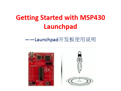
MSP430 LaunchPad 开发板【入门必看】
LaunchPad使用说明
CCS5.1的详细安装步骤参考CCS5.1User`s guide for MSP430.pdf,现在有破解版的CCS5.1。
Code Composer Studio (CCS5.1)
Workspace
Project 1
Project 2 Project 3 Settings and preferences
USI with I2C and SPI support USCI with I2C, SPI and UART support Inverting and non-inverting inputs Selectable RC output filter Output to Timer_A2 capture input Interrupt capability
GPIO Code Example
P1DIR |= BIT0; //设置 P1.0为输出 P1OUT |= BIT0; //P1.0 输出高电平
For GPIO 中断相关寄存器
详细的参考MSP430x2xxFamily user guide.pdf
主要内容
LaunchPad实验板介绍
开发环境介绍
LaunchPad的应用
演示LaunchPad的电容触摸板
详细参考:430BOOST-SENSE1.pdf
LaunchPad应用1
• 基于心电图的心率监测仪(EKG-Based Heart-Rate Monitor Implementation on the LaunchPad Using the MSP430G2452MCU)
Link
Project Project Project Source files
Link
launchpad说明
玩Launchpad必然少了编译环境,什么编译软件适合初学者呢?在我个人认为,也是众多友友的想法,CCS(Code Composer Studio)不及IAR(IAR Embedded Workbench IDE )使用方便,但CCS作为TI DSP的官方软件,其功能确实很强大!各取所长,下面就详细说下用IAR 为Launchpad开发C语言吧!操作系统:Windows 7开发环境:IAR FOR MSP430 V5.30.1第一步:驱动安装IAR FOR MSP430 V5.30.1软件已集成Launchpad驱动,安装好IAR再将Launchpad与电脑箱连接,等待驱动安装完毕就可以了,一般成功安装是没问题的!如果不成功,检查下电脑与板子连接是否完好。
IAR FOR MSP430 V5.30.1下载地址在下面附上。
下载网址:要先登录115网盘,没有的一下子就可以注册的,然后点存至网盘,在自己网盘就可以下载了!/file/anodidvs加个百度网盘下载地址:/share/link?shareid=32705&uk=503898939第二步:建立工程废话不多说,双击软件图标2012-8-22 23:29 上传下载附件(4.38 KB)打开工程,点击工具栏上方的File-New-Workspace,新建工作组,再点击工具栏Project-Creat New Project,转到如图,下载附件(44.98 KB)接着点击如图所示,2012-8-22 22:51 上传下载附件(28.69 KB)接着会提示你保存工程文件,存在事先建好的文件夹内.下载附件(59.97 KB)选择 C - main,这里也可以选择Empty project,但选择 C -main的话,它会自己帮你新建一个main.c文件,并且把它加入到工程中。
给指定一个文件,并且把它加入到工程中。
给指定的工程名称msp430中。
【LaunchPad】开发板介绍

LaunchPad开发板介绍前言大家都拿到了超级便宜的LaunchPad的开发板,这些开发板有的朋友是拿来学习的,有的只是看着便宜先入手一个。
无论大家是出于什么目的都无所谓,现在板子到手了,咱们就要把他利用起来。
咱们EE论坛这次展开LaunchPad的千人大学习,我算是抛砖引玉发出此贴,希望大家一起来编写LaunchPad的中文教材,打造中国最全面的LaunchPad中文教材。
闲话不说了,介绍我挑重点的说,尽量少说废话。
开始了!开发板介绍首先,LaunchPad是一个完整的开发板。
板上包括仿真器和目标芯片,通过仿真器我们可以在线控制CPU的运行以及查看硬件寄存器;目标芯片就是我们编写的代码要下载到的芯片。
在图1所示的开发板照片中,照片中用黄色方框框出来的是仿真器,蓝色方框框出来的是目标板,也就是我们编写的代码最终要运行的地方。
套件内容LaunchPad的开发板包括以下内容:1、LaunchPad开发板2、MinUSB电缆3、两块MSP430G系列芯片– MSP430G2231: 低功耗16位单片机,片上拥有10位8通道的ADC、2K容量的Flash和128bytes 的RAM– MSP430G2211: 低功耗16位单片机,包括一个片上比较器以及2K容量的Flash和128bytes的SRAM4、2排10针的排针和2排10针的插座5、一只32.768-kHz的晶体仿真器介绍大家拿到开发板的时候可以看到在仿真器中最大的那块芯片也是一款1xx系列的MSP430单片机,但我们的代码并不是在这块单片机上运行的,这块单片机其实是充当了仿真器的功能,代码真正还是在目标板上的目标芯片上运行。
在初学阶段的话不需要再仿真器上花时间,仅仅把它当做工具使用即可。
通过图片可以看到,仿真器和目标板之间是通过跳线连接的。
其实这暗示着LaunchPad 上的仿真器不止可以调试下载Gxxx系列的芯片,它还可以调试下载eZ430-RF2500T开发板、eZ430-F2012T/F2013T开发板以及eZ430-Chronos手表。
【Energia开发环境】MSP430 LAUNCHPAD学习笔记5--串口
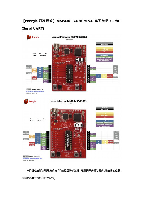
【Energia开发环境】MSP430LAUNCHPAD学习笔记5--串口(Serial UART)串口通信能够实现开发板与PC的相互传输数据,常用于开发板的调试,输出调试信息,直观的观察开发板运行的状况。
对于MSP430G2553的串口,需要注意的是由于LAUNCHPAD的版本不同,有1.4和1.5两个版本,如上图。
1.5版本的LAUNCHPAD可以在调试时直接使用硬件UART与电脑通信。
这次实验所使用的芯片型号为G2553,在包装和里也有G2452的芯片,所以要看清楚你所使用的是哪个芯片。
如果你手上正好有一块G25531.5版本的LAUNCHPAD,那就方便多了。
LAUNCHPAD板子上的仿真器串口最大通信速率为9600baud,我们在写程序的时候最好不要超过这个数值。
我们先来做个简单的串口实验:编写完程序后,连上板子,查看软件是否已正常连接开发板,然后下载程序。
常用函数:Serial.begin(speed):这个函数是对波特率的设定,常有的波特率有300,600,1200,2400, 4800,9600,14400,19200,28800,38400,57600,11520这些。
这里使用是9600baud。
print(val):在串口发送数据的时候,会将其转换为人类可阅读的ASCII字符。
∙Serial.print(78)输出"78"∙Serial.print(1.23456)输出"1.23"∙Serial.print('N')输出"N"∙Serial.print("Hello world.")输出"Hello world."也可以在print(val,format)中加入第二个参数,如:∙Serial.print(78,BIN)输出"1001110"∙Serial.print(78,OCT)输出"116"∙Serial.print(78,DEC)输出"78"∙Serial.print(78,HEX)输出"4E"∙Serial.println(1.23456,0)输出"1"∙Serial.println(1.23456,2)输出"1.23"∙Serial.println(1.23456,4)输出"1.2346"Serial.println(val,format)是print(val,)的加强版,只是在print生成的字符串后面加一个”\n”作为换行符。
MSP-EXP430G2开发板使用简单介绍

(4)、中断的嵌套:
当同时有多个中断来的时候才有优先级的考虑(优先级顺序可查看向量表)
实现中断嵌套需要注意以下几点: 1)430默认的是关闭中断嵌套的,一定要中断嵌套的话,就必须在中断服务程序中打开 总中断 msp430的指令中,_DINT()和_EINT()分别指关和开总中断。 2)当进入中断服务程序时,只要不在中断服务程序中再次开中断,则总中断是关闭的, 此时来中断不管是比当前中断的优先级高还是低都不执行; 3)若在中断服务程序A中开了总中断,则可以响应后来的中断B(不管B的优先级比A高 还是低),B执行完再继续执行A。注意:进入中断服务程序B后总中断同样也会关闭, 如 果B中断程序执行时需响应中断C,则此时也要开总中断,若不需响应中断,则不用 开中断,B执行完后跳出中断程序进入A程序时,总中断会自动打开; 4)若在中断服务程序中开了总中断,后来的中断同时有多个,则会按优先级来执行,即 中断优先级只有在多个中断同时到来时才起做用!中断服务不执行抢先原则。 5)对于单源中断,只要响应中断,系统硬件自动清中断标志位,对于TA/TB定时器的比较/捕 获中断,只要访问TAIV/TBIV,标志位倍被自动清除; 对于多源中断要手动清标志位,比如P1/P2口中断,要手工清除相应的标志,如果在这种中 断用"EINT();"开中断,而在打开中断前没有清标志,就会 有相同的中断不断嵌入,而导致 堆栈溢出引起复位,所以在这类中断中必须先清标志再打开中断开关.
Clock
FLASH
... JTAG/Debug
RAM
MAB 16
RISC CPU 16-bit
MDB 16
...
ACLK SMCLK
Digital Peripheral
Analog Peripheral
launchpad

单片机编程学习入门LaunchPad板实验报告一、LaunchPad实验板简介1概述名为LaunchPad的MSP-EXP430G2低成本试验板是一款适用于TI最新MSP430G2xx 系列产品的完整开发解决方案。
其基于USB的集成型仿真器可提供为全系列MSP430G2xx 器件开发应用所必需的所有软、硬件。
LaunchPad具有集成的DIP目标插座,可支持多达20个引脚,从而使MSP430ValueLine器件能够简便地插入LaunchPad电路板中。
此外,其还可提供板上Flash仿真工具,以直接连接至PC轻松进行编程、调试和评估。
LaunchPad试验板还能够对eZ430-RF2500T目标板、eZ430-Chronos手表模块或eZ430-F2012T/F2013T 目标板进行编程。
此外,它还提供了从MSP430G2xx器件到主机PC或相连目标板的9600波特UART串行连接。
详细可访以下了解更多/index.php/MSP430_LaunchPad_(MSP-EXP430G2) MSP-EXP430G2LaunchPad特性:•USB调试与编程接口无需驱动即可安装使用,且具备高达9600波特的UART串行通信速度•支持所有采用PDIP14或PDIP20封装的MSP430G2xx和MSP430F20xx器件•分别连接至绿光和红光LED的两个通用数字I/O引脚可提供视觉反馈•两个按钮可实现用户反馈和芯片复位•器件引脚可通过插座引出,既可以方便的用于调试,也可用来添加定制的扩展板•高质量的20引脚DIP插座,可轻松简便地插入目标器件或将其移除2安装安装MSP-EXP430G2LaunchPad时包含三个简单步骤:1.下载所需软件2.安装选定的IDE3.将LaunchPad连接至PC然后可使用LaunchPad开发应用或播放预先编好程的演示应用。
3.开始使用首次使用MSP-EXP430G2LaunchPad试验板时,演示应用将在该板从USB主机获得供电时立即自动启动。
MSP430入门

MSP430入门硬件初步这只是我在学习TI公司生产的16位超的功耗单片机MSP430的随笔,希望能对其他朋友有所借鉴,不对之处还请多指教。
下面,开始430之旅。
讲解430的书现在也有很多了,不过大多数都是详细说明底层硬件结构的,看了不免有些空洞和枯燥,我认为了解一个MCU的操作首先要对其基础特性有所了解,然后再仔细研究各模块的功能。
1.首先你要知道msp430的存储器结构。
典型微处理器的结构有两种:冯。
诺依曼结构——程序存储器和数据存储器统一编码;哈佛结构——程序存储器和数据存储器;msp430系列单片机属于前者,而常用的mcs51系列属于后者。
0-0xf特殊功能寄存器;0x10-0x1ff外围模块寄存器;0x200-?根据不同型号地址从低向高扩展;0x1000-0x107f seg_b0x1080_0x10ff seg_a 供flash信息存储剩下的从0xffff开始向下扩展,根据不同容量,例如149为60KB,0xffff-0x11002.复位信号是MCU工作的起点,430的复位信号有两种:上电复位信号POR和上电清除信号PUC。
POR 信号只在上电和RST/NMI复位管脚被设置为复位功能,且低电平时系统复位。
而PUC信号是POR信号产生,以及其他如看门狗定时溢出、安全键值出现错误是产生。
但是,无论那种信号触发的复位,都会使msp430在地址0xffff处读取复位中断向量,然后程序从中断向量所指的地址开始执行。
复位后的状态不写了,详见参考书,嘿嘿。
3.系统时钟是一个程序运行的指挥官,时序和中断也是整个程序的核心和中轴线。
430最多有三个振荡器,DCO内部振荡器;LFXT1外接低频振荡器,常见的32768HZ,不用外接负载电容;也可接高频450KHZ -8M,需接负载电容;XT2接高频450KHZ-8M,加外接电容。
(经验中发现,接XT2时,需要注意自己开启XT2,并延时50us等待XT2起振,然后手工清除IFG1中的OFIFG位,其操作顺序为:打开XT2->等待XT2稳定->切换系统时钟为XT2)430有三种时钟信号:MCLK系统主时钟,可分频1 2 4 8,供cpu使用,其他外围模块在有选择情况下也可使用;SMCLK系统子时钟,供外围模块使用,可选则不同振荡器产生的时钟信号;ACLK辅助时钟,只能由LFXT1产生,供外围模块。
LaunchPad入门指南

Introduction As applications continue to advance, 8-bit mi-crocontrollers are struggling to meet the growing demand for higher performance and ultra-low power to support evolving product designs. Texas Instruments introduced the affordable 16-bit MSP430™ MCU Value Line to meet the changing market dynamics and requirements faced by typical low-cost 8-bit MCU develop-ers. Taking the next step in providing a low-cost solution to the shortcomings of 8-bit MCUs, TI created the MSP430 MCU Value Line LaunchPad development kit to jump start application designs and provide a low-cost tool for developers of all experience levels. This overview will provide an introduction to the features and functionality of LaunchPad as well as everything included in the $4.30 kit. MSP430 Value Line LaunchPad Development KitAs the number of competitors grow and the time for taking products to market shrinks, the microcontroller (MCU) industry is being stretched by two opposing, but equally strong vectors. The growing demand for higher performance and ultra-low power functionality is matched only by an aggressive need for lower and lower price points. This is especially clear in low-cost applications that utilize 8-bit MCUs. To increase performance without breaking the bank, developers of low-cost 8-bit MCUs must migrate to higher performance 16-bit MCUs that are available at affordable price points.In high volume and quick turnover markets such as consumer and personal electronics, the need for a highly differentiated MCU, while maintaining aggressive price points, is a constant struggle. For instance, the market for 3D glasses has exploded in the recent months, both on the big and small screen. As this market trend moves up and to the right, developers are hard at work in creating technological solutions that provide a unique and immersive experience while remaining affordable. By providing more affordable solutions, developers hope to minimize the risks and barriers associated with new and fast moving markets.For many, this barrier to success is prohibited by a limited MCU core. Many developersof 8-bit MCUs have completely exhausted the full capabilities of their MCU due to limited data throughput and inefficient interfacing with higher resolution analog and digital peripherals. To enable increased functionality and improve feature sets of existing projects, developers must migrate to higher performance 16-bit MCUs.The MSP430 MCU Value Line series provides a migration path for many of these constrained 8-bit MCU developers. At no additional cost, the affordable MSP430 MCU Value Line devices offer a 16-bit architecture, higher precision timers and improved peripheral integration and interfacing, enabling improved performance and lower power consumption. The implementation of 16-bit MCUs enable up to 10 times improved performance and10 times lower power when compared to many low-cost 8-bit applications. Currently, the MSP430 MCU Value Line series offers 27 ultra-low power 16-bit devices that offer varying levels of analog integration, communication modules and package types. At 100K unit volumes, MSP430 MCU Value Line devices start at just $0.25 USD, ensuring thatAdrian FernandezMSP430 MicrocontrollersTexas Instruments W H I T E P A P E R2Texas Instrumentsdevelopers do not have to sacrifice price for improved performance. Additionally, the MSP430 MCUValue Line series will continue to grow to more than 100 devices through the second half of 2011.This roadmap will introduce higher memory sizes, more package options and additional integrated analogand digital peripherals.To make the transition from 8- to 16-bit MCUs more seamless, Texas Instruments (TI) listened to therequirements of developers and created the new MSP430 MCU Value Line LaunchPad development kit.Furthering the commitment to add performance and value to MCU designs with the MSP430 MCU ValueLine, TI introduced LaunchPad to lower the barrier of entry for developers new to 16-bit architectures, orthose new to MCU design, in general. The LaunchPad kit is TI’s simple, yet thorough, introduction to 16-bitMCU development, offering all of the hardware and software a developer needs to get started for just $4.30USD. Within minutes of opening the LaunchPad kit, users can begin interfacing with push buttons, LEDsand the on-chip peripherals of the MSP430 MCU Value Line devices. See Figure 1 below:For just $4.30, the LaunchPad kit includes a development board with an integrated USB-powered flashemulation tool for programming and debugging any of the existing MSP430 MCU Value Line devices. AnyMSP430G2xx MCU in a DIP package can be dropped into the DIP target socket of LaunchPad, which allowseasy evaluation of any MSP430 MCU Value Line device. The flexible target socket allows developers toremove their freshly programmed and debugged MSP430G2xx MCU to be plugged into a custombreadboard or PCB so that customers are not constrained to the form factor of the LaunchPad board.Alternatively, developers can use LaunchPad as a standalone system, by leaving the MSP430G2xx deviceplugged into the board to leverage on-board and programmable push buttons and LEDs. Additionally, everypin of the MSP430G2xx device is fully accessible, allowing easy interfacing of external components orcustom daughter cards. Figure 1.3Texas Instruments Figure 2. $4.30 LaunchPad kit offers the hardware and software needed to start developing applications, and is backed by an active online community to quicken time to market.Also provided in the kit are free, downloadable software compilers and debuggers including TI’s owneclipse-based Code Composer Studio™ version 4 and IAR Embedded Workbench Kickstart. Theseindependent development environments (IDEs) are full featured and are completely compatible withLaunchPad and the MSP430 MCU Value Line devices available today. This complements the hardwarefeatures of the LaunchPad board by providing a complete software component as well. Using either IDE,users can then leverage MSP430 MCU code examples, open source projects and other free onlineresources, which can be accessed on LaunchPad’s Wiki page, /launchpadwiki .The unlimited access to the LaunchPad Wiki promotes collaboration and simple sharing of solutions andideas, making LaunchPad a complete development environment. This active and growing online communitysupplements the hardware and software components of the LaunchPad package and provides instantsupport, projects and helpful hints that will be shared through the Wiki pages and E2E™ forums.To fully benefit from 16-bit architecture and ultra-low power performance, the MSP430 MCU Value Lineseries and LaunchPad development kit offers a complete and simple introduction to quicken developers’time to market. By providing 16-bit performance at 8-bit price points, and complete development tools forjust $4.30, TI would like to welcome both new and experienced users to the world of high performanceand affordable MCU development.A042210Important Notice: The products and services of Texas Instruments Incorporated and its subsidiaries described herein are sold subject to TI’s standard terms and conditions of sale. Customers are advised to obtain the most current and complete information about TI products and services before placing orders. TI assumes no liability for applications assistance, customer’s applications or product designs, software performance, or infringement of patents. The publication of information regarding any other company’s products or services does not constitute TI’s approval, warranty or endorsement thereof.The Platform Bar, MSP430, Code Composer Studio and E2E are trademarks of Texas Instruments.All other trademarks are the property of their respective owners.IMPORTANT NOTICETexas Instruments Incorporated and its subsidiaries(TI)reserve the right to make corrections,modifications,enhancements,improvements, and other changes to its products and services at any time and to discontinue any product or service without notice.Customers should obtain the latest relevant information before placing orders and should verify that such information is current and complete.All products are sold subject to TI’s terms and conditions of sale supplied at the time of order acknowledgment.TI warrants performance of its hardware products to the specifications applicable at the time of sale in accordance with TI’s standard warranty.Testing and other quality control techniques are used to the extent TI deems necessary to support this warranty.Except where mandated by government requirements,testing of all parameters of each product is not necessarily performed.TI assumes no liability for applications assistance or customer product design.Customers are responsible for their products and applications using TI components.To minimize the risks associated with customer products and applications,customers should provide adequate design and operating safeguards.TI does not warrant or represent that any license,either express or implied,is granted under any TI patent right,copyright,mask work right, or other TI intellectual property right relating to any combination,machine,or process in which TI products or services are rmation published by TI regarding third-party products or services does not constitute a license from TI to use such products or services or a warranty or endorsement e of such information may require a license from a third party under the patents or other intellectual property of the third party,or a license from TI under the patents or other intellectual property of TI.Reproduction of TI information in TI data books or data sheets is permissible only if reproduction is without alteration and is accompanied by all associated warranties,conditions,limitations,and notices.Reproduction of this information with alteration is an unfair and deceptive business practice.TI is not responsible or liable for such altered rmation of third parties may be subject to additional restrictions.Resale of TI products or services with statements different from or beyond the parameters stated by TI for that product or service voids all express and any implied warranties for the associated TI product or service and is an unfair and deceptive business practice.TI is not responsible or liable for any such statements.TI products are not authorized for use in safety-critical applications(such as life support)where a failure of the TI product would reasonably be expected to cause severe personal injury or death,unless officers of the parties have executed an agreement specifically governing such use.Buyers represent that they have all necessary expertise in the safety and regulatory ramifications of their applications,and acknowledge and agree that they are solely responsible for all legal,regulatory and safety-related requirements concerning their products and any use of TI products in such safety-critical applications,notwithstanding any applications-related information or support that may be provided by TI.Further,Buyers must fully indemnify TI and its representatives against any damages arising out of the use of TI products in such safety-critical applications.TI products are neither designed nor intended for use in military/aerospace applications or environments unless the TI products are specifically designated by TI as military-grade or"enhanced plastic."Only products designated by TI as military-grade meet military specifications.Buyers acknowledge and agree that any such use of TI products which TI has not designated as military-grade is solely at the Buyer's risk,and that they are solely responsible for compliance with all legal and regulatory requirements in connection with such use. TI products are neither designed nor intended for use in automotive applications or environments unless the specific TI products are designated by TI as compliant with ISO/TS16949requirements.Buyers acknowledge and agree that,if they use any non-designated products in automotive applications,TI will not be responsible for any failure to meet such requirements.Following are URLs where you can obtain information on other Texas Instruments products and application solutions:Products ApplicationsAmplifiers Audio /audioData Converters Automotive /automotiveDLP®Products Communications and /communicationsTelecomDSP Computers and /computersPeripheralsClocks and Timers /clocks Consumer Electronics /consumer-appsInterface Energy /energyLogic Industrial /industrialPower Mgmt Medical /medicalMicrocontrollers Security /securityRFID Space,Avionics&/space-avionics-defenseDefenseRF/IF and ZigBee®Solutions /lprf Video and Imaging /videoWireless /wireless-appsMailing Address:Texas Instruments,Post Office Box655303,Dallas,Texas75265Copyright©2010,Texas Instruments Incorporated。
MSP430 G2 LaunchPad使用入门

MSP430 G2 LaunchPad使用入门v1.0 2013.8.8xie_sx@目录目录 (1)1 G2 LaunchPad功能简介 (1)1.1 快速入门 (1)1.2 硬件电路 (3)1.3 片上资源 (4)1.4 自学资料 (5)1G2 LaunchPad功能简介1.1快速入门收到MSP430 LaunchPad G2板卡,完整包装盒如下所示:打开盒子,MSP-EXP430G2 套件盒包括下列物品:•MSP-EXP430G2板卡•USB线•两个10 脚单排孔(暂时用不上)•1个32.768kHz 时钟晶振(该晶振不焊接,单片机使用的是内部晶振,建议焊接上)•一张快速启动指南+两个LaunchPad 贴签•两个MSP430 单片机–MSP430G2553:具有8 通道10 位模数转换器(ADC)、片上比较器、触控式使能I/O、通用串行通信接口、16kB 闪存、和512 字节RAM 的低功耗16 位MSP430 微控制器(预加载有示例程序)–MSP430G2452:具有8 通道10 位ADC、片上比较器、触控式I/O、通用串行接口、8kB 闪存、和256 字节SRAM 的低功耗16 位MSP430 微控制器拆开包装,拿出G2板卡,电路板如下图所示:作为入门使用的电路板,在设计入门实验时,我们更多的是借助两个LED灯和一个按键,进行单片机功能模块的学习。
在电脑上安装CCS软件,接着用USB线连接电脑和G2板卡,简单两个步骤就可以开始单片机的实验了。
基本的实验环境搭建好之后,如下图所示。
在宿舍/教室/图书馆等地方,仅需外带一台电脑就可以做实验了。
1.2硬件电路在嵌入式的学习过程中,硬件知识是必不可少的。
对于初学者来说,仿真器部分的具体电路可以跳过,把精力放在单片机核心板卡上。
G2板卡硬件电路较为简单,将所有的IO口引出,并且配有两个LED知识灯+1个用户按键输入。
电源供电部分的电路如下所示,通过电脑的USB口获取5V的电源输入,经稳压芯片稳压后输出3.6V电压给单片机供电。
【LaunchPad】触摸板试用心得 (1)

MSP430 LaunchPad触摸板试用心得
1、硬件环境搭建
(1)、将开发板上的G2231芯片换成附赠的G2211,因为G2231不带比较器,只有G2211才带,2231带SPI和串口等
(2)、将开发板上的R34和C24焊下,焊接时小心,我就是焊接时把PCB焊坏了,这两个贴片是焊补上去了,到时只有飞线了,郁闷:(
(3)、改跳线,将开发板的J3的RXT、TXD断开,将J5的两个跳线断开
(4)、将LaunchPad TOUCH子板插入到开发板上
2、软件环境搭建
我是使用的IAR5.1,没有使用CCS,安装好后,新建一个WORKSPACE,再新建一个PROJECT,加入现有文件将TI的例程Cap_Sensing_Touch_Key_V1.0.c加入,修改项目的选项
选择芯片类型为2211
编译程序,主要修改仿真项如下,不然程序只是在电脑上仿真不能下载到板子上
好了,现在大家可以在线仿真测试触摸板的魅力了,感觉LED闪屏的频率分级不明显。
一共两个工程,另一个需要跳触摸屏子板上的跳线。
MSP-EXP430G2入门

提纲:一.MSP-EXP430G2套件介绍1.包装清单unchPad简介(430文件夹_用户指南)(一)LaunchPad片上资源(1)开发板硬件简介(2)主要功能模块(二)LaunchPad特性(三)LaunchPad电路图(主要参考【LaunchPad】开发板介绍.pdf)3.MSP430G2553数据资料(技术资料汇总_G2553中文资料.pdf)4.安装MSP-EXP430G2 LaunchPad二.编译部分1.编译工具的选择2.编译工具的安装(根据安装提示便可)3.程序编译、烧录流程4.编程规则(MSP430 编程规则.pdf)三.基础程序部分1.功能模块程序(MSP430G2xx3 Code Examples文件夹)2.基础应用程序(例程代码)四.应用举例——MSP430G2452内置温度传感器温度检测五.LaunchPad扩展部分1.eZ430连接、编程要点2.与卫星板的连接3.与LaunchPad兼容的MSP430器件一.MSP-EXP430G2套件介绍1.包装清单:⏹LaunchPad目标板(附一个烧好测温实验例程的MPS430G2553)⏹MPS4302452一个——具有8通道10位ADC、片上比较器、触控式I/O、通用串行接口、8Kb闪存、256字节SRAM的低功耗16位MSP430微控制器⏹32.768KHz时钟晶振⏹0.5m长的USB-B线缆⏹插座式10引脚印刷板连接线两个⏹LaunchPad贴签两个⏹快速启动指南unchPad简介(一)LaunchPad片上资源(1)开发板硬件介绍:板上材料清单开发板指示图(2)主要功能模块:⏹复位模块⏹时钟模块⏹I/O端口模块;⏹WDT看门狗模块;⏹Timer A定时器模块⏹比较器A模块⏹ADC10数模转换模块⏹USART串行异步通讯模块⏹CPU模块(二)LaunchPad特性⏹实验班成本低、低功耗⏹USB调试与编程接口无需驱动即可安装使用,且具备高达9600波特的UART串行通信速度⏹支持所有采用PDIP14或PDIP20封装的MSP430G2XX和MSP430F20XX器件⏹分别连接至绿光和红光LED的两个通用数字I/O口引脚可提供视觉反馈⏹两个按钮可实现用户反馈和芯片复位⏹器件引脚可通过插座引出,既可以方便的用于调试,也可用来添加定制的扩展板⏹高质量的20引脚DIP插座,可轻松简便地插入目标器件或将其移除(三)LaunchPad电路图LaunchPad原理图见“【LaunchPad】开发板介绍.pdf”。
MSP430学习笔记

图和下方CCR2的框图是一样的。此处省略不写。在CCR中, 左上角为一个捕获源选择寄存器。可以从CCI2A、CCI2B、 GND或者VCC选择捕获源,选择捕获源后有一个选择捕获模 式寄存器Capture Mode,然后过来有一个捕获溢出状态寄 存器COV,SCS同步/异步捕获模式选择位,然后连接到捕获 比较寄存器。下方为模式选择寄存器,具体设置可以查看相 应的寄存器设置。 这里仅是大概介绍一下Timer0的寄存器,具体的设置使用还 看参考相应的寄存器并结合例程慢慢学习理解。
//以下为参考处理程序,不使用的端口应当删除其对于中断源的判断。 if((P1IFG&BIT0) == BIT0) { P2OUT&=~BIT0; //处理P1IN.0中断 P1IFG &= ~BIT0; //清除中断标志 //以下填充用户代码 } else if((P1IFG&BIT1) ==BIT1) { P2OUT&=~BIT1; //处理P1IN.1中断 P1IFG &= ~BIT1; //清除中断标志 //以下填充用户代码 } else if((P1IFG&BIT2) ==BIT2) { P2OUT&=~BIT2; //处理P1IN.2中断 P1IFG &= ~BIT2; //清除中断标志 //以下填充用户代码 } else if((P1IFG&BIT3) ==BIT3) { //处理P1IN.3中断 P1IFG &= ~BIT3; //清除中断标志 //以下填充用户代码 } else if((P1IFG&BIT4) ==BIT4) { P2OUT&=~BIT4; //处理P1IN.4中断 P1IFG &= ~BIT4; //清除中断标志 //以下填充用户代码 } else if((P1IFG&BIT5) ==BIT5) { //处理P1IN.5中断 P1IFG &= ~BIT5; //清除中断标志 //以下填充用户代码 } else if((P1IFG&BIT6) ==BIT6) { //处理P1IN.6中断 P1IFG &= ~BIT6; //清除中断标志 //以下填充用户代码
【LaunchPad】学习第一记
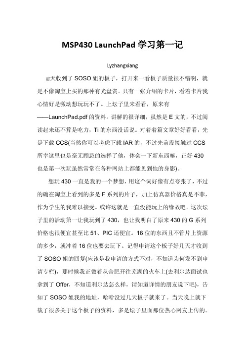
MSP430 LaunchPad学习第一记Lyzhangxiang前天收到了SOSO姐的板子,打开来一看板子质量很不错啊,就是不像淘宝上买的那种有光盘资。
只有一张介绍的卡片,看着卡片我心情好是激动想玩玩不了。
上坛子里来看看,原来有——LaunchPad.pdf的资料。
讲解的很详细,虽然是E文的,不过阅读起来还不算是吃力,Ti的东西没话说。
对着着篇文章好好看看,先是下载CCS(当然你可以考虑下载IAR的,不过先前没接触过CCS 所幸这里也是毫无顾忌的选择了他,体会一下新东西嘛,正好430也是第一次玩虽然常常在各种网站上都能见到他的身影)。
想玩430一直是我的一个梦想,用这个词好像有点夸张了,不过的确在淘宝上看到的多是F系列的片子,加上仿真器价格真是不菲,作为学生的我难以接受。
或许这就是一直没能玩上的缘故吧。
这次坛子里的活动第一让我玩到了430,也让我明白了原来430的G系列价格也很便宜甚至比51、PIC还便宜。
16位的东西且不管片上资源的多少,就冲着16位也要去玩下。
记得申请这个板子好几天才收到了SOSO姐的回复(应该是我申请的方式不对,不知道为何发不到申请专栏),那时候我正做着从合肥开往芜湖的火车上(去利尔达面试也拿到了Offer,不知道利尔达怎么样,请知道详情的朋友说下吧),告知了SOSO姐我的地址,哈哈没过几天板子就来了。
当天晚上就下载了很多关于这个板子的资料,多是坛子里面那位热心网友上传的。
首先就是阅读了那个LaunchPad的pdf,然后下载CCS安装完毕,其次看了一下G2211和G2231的数据手册。
大概有个了解之后开始玩了,打开CCS新建工程,关于CCS的操作可以下载那个视频看一下啦,基本对付了。
哦忘了说了还有那个很不错的触摸板子,也有一篇很好的pdf叫——LaunchPad实验板触摸感应子卡使用指南。
原理图以及代码示例里面都有讲解的。
详细的操作我也不说了直接进入主题了,第一次嘛还是跑通Demo 的好,毕竟我是第一次搞430,也不知道代码需要怎样去写。
MSP430初学者教程(最详细)

如何学习MSP430单片机学习就是迎接挑战、解决困难的过程,没有挑战,就没有人生的乐趣。
下面以MSP430系列单片机为例,解释一下学习单片机的过程。
(1)获取资料购买有关书籍,并到杭州利尔达公司网站和TI网站获取资料,例如,在网上可以找到FET 使用指导、MSP430 F1xx系列、F4xx系列的使用说明和具体单片机芯片的数据说明,可以找到仿真器FET的电路图、实验板电路图、芯片封装知识等大量的实际应用参考电路,当然有些资料是英文的,看懂英文资料是个挑战,学会4、6级英语就是为看资料的。
英语难学,但是看资料容易,只要下决心,看完一本资料,就可以看懂所有的相关资料。
(2)购买仿真器FET和实验电路板如果经济条件不错,可以直接购买。
(3)自制仿真器FET和实验电路板自制仿真器FET,首先要到网上找到FET电路图,然后就可以使用画电路板软件画电路图和电路板图,这又是个挑战。
FET电路非常简单,但要把它制作出来还是需要下一番工夫的,找一本有关书,然后练习画原理图,画完原理图后,就学习认识元件封装,再购买元件,这时就可以画电路板图了,一旦画好,将形成的PCB文件交给电路板制作公司,10天后,就可以得到电路板,焊上元件和电缆,等实验电路板做好后,就可以与实验电路板一起调试了。
自制实验电路板,需要单片机芯片内部工作原理的知识、封装知识,清楚的知道每一个引脚的功能,还需要数码管、按钮、排电阻、三端稳压器、二极管、散热器、电解电容、普通电容、电阻、钮子开关等元件的知识,对于初学者,可以做一个只有3个数码管、8个按钮、8个发光二极管的简单实验板,这样的实验板,虽然简单,但足可以帮助初学者入门单片机。
自制实验电路板与自制FET一样,首先画电路图,然后买元件,再画电路板。
由于MSP430系列芯片是扁平封装,焊接起来有一定难度,这好象是个挑战,但实际上很简单,方法如下:首先在焊盘上涂上松香水,在松香水未干的情况下,将芯片放在焊盘上,注意芯片第一引脚的位置,并使引脚与焊盘对齐,将擦干净的电烙铁(不能有任何焊锡)接触引脚,引脚只要一热,焊盘上的焊锡就自动将引脚焊住了,千万注意电烙铁上不能有焊锡,焊接时最好配备一个放大镜。
MSP430开发板

DAC实验
(1) DAC手动测试
本例进行8位数字到模拟转换的实验,数模转换由TLV5620完成,它是有四个输出通道,试验使用通道A。输 出的模拟值再输入到430的模拟输入通道5(其他通道CPU不能使用,但可以使用数字表来检测,或者直接跳线到 有关输入),同样ADC12采用单通道重复采样模式。
(2) DAC正弦波发生
软件组成
1.基本时钟模块 2.端口模块 3.串口模块 4.定时器A模块 5. ADC12模块 6. I2C仿真模块 7. SPI仿真模块 8.外部DAC模块 9.外部I2C存储器扩展模块(选件) 10.外部液晶模块(仅EDB430B型)
硬件配置
EDB430开发实验系统采用: 1、MSP430F149CPU模块, 2、20字符x2行串行通信液晶模块,SPI接口 3、8MHz+32768晶振 4、外部模拟到数字转换器DAC,SPI接口 5、1个复位键、3×3可重配置扫描键 6、1个蜂鸣器 7、2个自动低功耗串口串口带连路指示 8、在板仿真工具(FET),无须再购买 9、2个LED指示 10、4个模拟缓冲器
本次试验分为两个部分,一是I2C协议的仿真软件,其二是键盘和LED控制实验,输入输出接口功能由 PCF8574完成。本例中,3×3键盘作为用户输入口,输入键值用超级终端作为观察窗口,配合相应的LED作为响应 指示,因此,在软件项目中需添加相应的串口模块。
ADC实验
本例对电源电压进行测量的实验,使用了430的模拟输入通道7,采用单通道重复采样模式,使用外部参考电 源(为了得到好的精度和稳定性)它的输入信号直接来自整流电源输出。
产品介绍
MSP430开发板推荐一个学习MSP430单片机的开发板,全一体,直接使用并口下载,MSP430F2272的开发板, 利挺好用的,适合学习,不贵。MSP430开发板采用MSP430F149 CPU芯片。是特别针对149中的新功能而开发的。 除了430的一般通用功能外,还可实现双12位D/A转换,DMA通道,IIC的硬件通讯。此学习板上可轻松实现测量系 统、数字处理系统(A/D,D/A)等工业控制中的实验。还可用于如数字马达控制、手持式仪表、光网络中的TEC 等等。
实验一CCS的入门操作

实验一CCS的入门操作实验准备:- 一台运行Windows操作系统的电脑- MSP430 LaunchPad开发板(或其他支持CCS的开发板)实验步骤:第一步:安装CCS2.安装完成后,启动CCS。
首次启动时,会有一个启动向导引导你设置CCS的工作环境。
按照提示进行设置。
第二步:创建一个新项目1. 在CCS的主界面上,点击“File” -> “New” -> “CCS Project”。
2.在弹出的对话框中,选择目标微控制器型号,例如MSP430G25533. 输入项目的名称和存储位置,并点击“Finish”按钮,CCS将创建一个新的项目。
第三步:编写代码1. 在项目导航器窗口中,展开“Source Files”文件夹,右键点击“main.c”,选择“Open With” -> “Text Editor”。
```c#include <msp430g2553.h>int main(void)WDTCTL=WDTPW+WDTHOLD;//停止看门狗定时器P1DIR,=BIT0;//将P1.0引脚设置为输出P1OUT&=~BIT0;//确保P1.0引脚是低电平while(1)P1OUT^=BIT0;//切换P1.0引脚的状态}```第四步:构建和调试1. 在项目导航器窗口中,右键点击项目名称,选择“Build”以构建项目。
CCS将编译项目并生成可执行文件。
2. 将MSP430 LaunchPad开发板与电脑连接,并通过USB线缆进行供电。
3. 点击CCS界面上的“Debug”按钮,CCS将自动连接到开发板并启动调试器。
4. 在调试器界面上,点击“Resume”按钮,CCS将开始执行你的代码。
第五步:观察结果1.如果一切顺利,开发板上的LED应该开始闪烁。
你可以在CCS的调试器界面上观察程序的执行过程,并通过设置断点来调试代码。
总结:本实验介绍了CCS的基本操作流程,包括安装CCS、创建新项目、编写代码、构建和调试。
S.D.Lu的MSP430入门学习笔记(2):GPIO

本实验所用的硬件是TI的MSP-EXP430G2 LaunchPad 试验板。
原理图如下。
软件在一篇的基础上进行修改。
将main函数改为如下内容:编译完成后,点击下载调试按钮,将代码下载到实验板上。
P1.0和P1.6上的LED轮流点亮和熄灭。
代码解释:9~11行,对IO端口进行设置时,用到了BITx。
这是头文件中定义的,用于位操作的宏定义,比较方便的操作各个IO端口。
因为MSP430的IO是双向的,所以在使用之前需设置其方向。
15行,定义了一个变量i,在IAR环境下允许用户在程序段中间定义变量。
17行,将P1.0和P1.6的输出和(BIT0 + BIT6)进行异或,其结果相当于将P1.0和P1.6输出进行取反。
GPIO的一般操作如果不涉及片内外设,对GPIO的操作只涉及4个寄存器:PxDIR、PxOUT、PxIN、PxREN。
PxDIR用于设置GPIO的方向,PxOUT用于设置输出值,PxIN用于读取输入值。
PxREN用于GPIO内置的上拉/下拉电阻。
当PxREN.bit=1,上拉/下拉电阻被使能,PxOUT.bit=0为下拉,=1为上拉。
具体如何操作,可参考TI官方例程“msp430g2xx2_P1_01.c”、“msp430g2xx2_P1_03.c”两个程序运行的结果都是:P1.0的输出跟随P1.4的输入电平变化。
对于不使用的IO应避免设置成悬空输入。
P1、P2口的中断MSP430的P1、P2口每一个引脚都有中断的功能,P1的所有引脚的中断共用一个中断向量,P2口与P1口类似。
P1、P2口中断功能相关的寄存器有3个,PxIFG、PxIE和PxIES。
PxIFG是中断标志寄存器,用于指示哪一个IO上产生了中断。
PxIE是中断使能寄存器,PxIES 是中断边沿选择寄存器。
各个寄存器取值所对应的功能请参考《用户指南》。
P1、P2口中断功能的使用可参考TI官方例程“msp430g2xx2_P1_02.c”、“msp430g2xx2_P1_04.c”,这两个例程分别是在TI官方例程“msp430g2xx2_P1_01.c”、“msp430g2xx2_P1_03.c”基础上修改的,将IO输入识别功能用中断功能来实现。
MSP430单片机,7讲

任务分析:
1、系统时钟配置
2、看门狗配置
3、端口配置
4、低功耗(中断)配置
程序代码:
#include <msp430G2553.h> void main(void) { BCSCTL1=CALBC1_1MHZ;//BCSCTL1=RSEL0+RESL1+RSE2 DCOCTL=CALDCO_1MHZ;//DCOCTL=DCO1+DCO2; BCSCTL2|=SELM_1+DIVS_3;//选择SMCLK为8分频 WDTCTL=WDT_MDLY_32;//看门狗延时32*8=256ms IE1|=WDTIE; P1DIR|=BIT0; _EINT(); for(;;) { LPM0;_NOP();} } #pragma vector=WDT_VECTOR __interrupt void watchdog_timer(void) { P1OUT^=BIT0;}
MSP430低功耗单片机
第7讲 MSP430 lauchpad的应用
开发板(launchpad)的优势
1、轻巧便利,是口袋实验室计划的 实施平台 2、方便的电源设置 3、方便的驱动方案 4、简洁、有效的调试步骤
开发板平面图
任务:设置一个看门狗定时程序, 让P1.0(LED1)在看门狗定时 到后取反,即LED1闪烁
任务:设置P1.3为按键,P1.0控 制LED1。按下P1.3让P1.0取反。 即LED1闪烁
任务分析:
1、看门狗停序代码:
#include <msp430G2553.h> void main(void) { WDTCTL=WDTPW+WDTHOLD; P1DIR|=BIT0; P1IFG&=~BIT3;//清除标志位 P1IE|=BIT3;//开中断使能 P1IES|=BIT3;//设置触发方式 _EINT();//开总中断允许 for(;;) { LPM4;_NOP();}//无需CPU,无需振荡器,无需辅助时钟 } #pragma vector=PORT1_VECTOR __interrupt void port1(void) { unsigned int i; P1IFG&=~BIT3;//清除标志位 for(i=0;i<10000;i++);//延时消抖 do{ P1IFG&=~BIT3; } while(P1IFG&BIT3);//反复清除标志位直到标志位为0 P1OUT^=BIT0;//P1.0取反 }
- 1、下载文档前请自行甄别文档内容的完整性,平台不提供额外的编辑、内容补充、找答案等附加服务。
- 2、"仅部分预览"的文档,不可在线预览部分如存在完整性等问题,可反馈申请退款(可完整预览的文档不适用该条件!)。
- 3、如文档侵犯您的权益,请联系客服反馈,我们会尽快为您处理(人工客服工作时间:9:00-18:30)。
LaunchPad 开发板介绍
前言
大家都拿到了超级便宜的LaunchPad 的开发板,这些开发板有的朋友是拿来学习的,有
的只是看着便宜先入手一个。
无论大家是出于什么目的都无所谓,现在板子到手了,咱们就要把他利用起来。
咱们EE 论坛这次展开LaunchPad 的千人大学习,我算是抛砖引玉发出此
贴,希望大家一起来编写LaunchPad 的中文教材,打造中国最全面的LaunchPad 中文教材。
闲话不说了,介绍我挑重点的说,尽量少说废话。
开始了!
开发板介绍
首先,LaunchPad 是一个完整的开发板。
板上包括仿真器和目标芯片,通过仿真器我们
可以在线控制CPU 的运行以及查看硬件寄存器;目标芯片就是我们编写的代码要下载到的芯片。
在图1 所示的开发板照片中,照片中用黄色方框框出来的是仿真器,蓝色方框框出来
的是目标板,也就是我们编写的代码最终要运行的地方。
套件内容
LaunchPad 的开发板包括以下内容:
1 、LaunchPad 开发板
2 、MinUSB 电缆
3 、两块MSP430G 系列芯片
–MSP430G2231: 低功耗16位单片机,片上拥有10位8 通道的ADC、2K容量的Flash 和128bytes
的RAM
–MSP430G2211: 低功耗16位单片机,包括一个片上比较器以及2K容量的Flash和128bytes的
SRAM
4 、2 排10针的排针和2 排10针的插座
5 、一只32.768- kHz 的晶体
仿真器介绍
大家拿到开发板的时候可以看到在仿真器中最大的那块芯片也是一款1xx 系列的
MSP430单片机,但我们的代码并不是在这块单片机上运行的,这块单片机其实是充当了仿真器的功能,代码真正还是在目标板上的目标芯片上运行。
在初学阶段的话不需要再仿真器上花时间,仅仅把它当做工具使用即可。
通过图片可以看到,仿真器和目标板之间是通过跳线连接的。
其实这暗示着LaunchPad
上的仿真器不止可以调试下载Gxxx 系列的芯片,它还可以调试下载eZ430 - RF2500T开发板、
eZ430 - F2012T/F2013T开发板以及eZ430 - Chronos 手表。
它还有一个重要的功能是提供了目标
板串口到PC的链接,串口速率为9600。
仿真器使用的是minUSB接口,USB电缆在开发套件中
包含。
可以利用IA R(For MSP430 )集成开发环境或者TI 自己推出的CCS(Code Composer Studio)
对应用进行仿真、调试以及下载。
仿真器对全速硬件断点以及单步执行是完全支持的。
图1 开发板实物
目标板介绍
目标板上有一个20针的DIP 插座可以用于更换MSP430单片机,芯片所有管脚全部通
仿
目标板介绍
目标板上有一个20针的DIP 插座可以用于更换MSP430单片机,芯片所有管脚全部通
仿真器
目标板
2 LED 按键
过开发板两侧的排插引出,可以比较方便的进行拓展实验,比如焊上排针插座后就可以使用触摸板(LaunchPad 套件本身不包含)。
板上还有2 个LED 和一个通用按键,还有一个按键
旁边标有reset是复位按键。
板上有很多的跳线J1 和J2 是将IO 引出的比较容易理解。
J3 是用于和eZ430 开发板连接的跳线。
J4是仿真器和目标板间连接跳线其功能如下表所示:
J5 选择MSP430的IO 接口P1.0 和P1.6 和LED 的连接,J6 是用于外部供电。
具体的连
接可以参考附
录中的电路图(MSP-EXP430G2 LaunchPad Experimenter Board User's Guide的电路图部分)。
本文大量参考了MSP-EXP430G2 LaunchPad Experimenter Board User's Guide 内容,文档号SLAU318。
海盗郭兆广
2012- 06-14。