在复合金属纳米结构中的等离子体
基于表面等离子体共振效应的Ag(Au)

2016年第35卷第1期CHEMICAL INDUSTRY AND ENGINEERING PROGRESS ·131·化工进展基于表面等离子体共振效应的Ag(Au)/半导体纳米复合光催化剂的研究进展邵先坤,郝勇敢,刘同宣,胡路阳,王媛媛,李本侠(安徽理工大学材料科学与工程学院,安徽淮南 232001)摘要:由具有表面等离子体共振(surface plasmon resonance,SPR)效应的贵金属(Ag、Au等)纳米粒子和半导体纳米结构组成的纳米复合光催化剂具有优异的可见光光催化活性,成为新型光催化材料的研究热点之一。
本文综述了Ag(Au)/半导体纳米复合光催化剂的制备方法、基本性质以及光催化应用方面的一些重要研究进展;重点介绍了Ag(Au)等纳米粒子的表面等离子共振增强可见光催化活性的机理,以及Ag(Au)纳米粒子与不同类型半导体复合的光催化剂的光催化性能,其中所涉及的半导体包括金属氧化物、硫化物和其他一些半导体;本领域未来几年的研究热点将集中于新型高效的Ag(Au)/半导体纳米复合光催化剂的微结构调控及其用于可见光驱动有机反应的机理研究。
本文为基于SPR效应构建Ag(Au)/半导体纳米复合光催化剂的研究提供了有力的参考依据,并且指出Ag(Au)/半导体纳米复合光催化剂的研究是发展可见光高效光催化剂的重要方向。
关键词:贵金属;表面等离子体共振;可见光响应;催化剂;降解;制氢中图分类号:O 649.2 文献标志码:A 文章编号:1000–6613(2016)01–0131–07DOI:10.16085/j.issn.1000-6613.2016.01.017Research progress of Ag(Au)/semiconductor nanohybrid photocatalystsbased on surface plasmon resonanceSHAO Xiankun,HAO Yonggan,LIU Tongxuan,HU Luyang,WANG Yuanyuan,LI Benxia (School of Materials Science and Engineering,Anhui University of Science and Technology,Huainan 232001,Anhui,China)Abstract:Nanohybrid photocatalysts composed of noble metal nanoparticles (Ag,Au,etc.) with surface plasmon resonance (SPR) effect and semiconductor nanostructures have become one of the research hotspots in the field of advanced photocatalysis because of their excellent photocatalytic activity under visible light irradiation. This review summarized some significant research progress about the basic properties,preparation methods and the photocatalytic applications of the plasmonic Ag(Au)/semiconductor nanohybrid photocatalysts. We emphatically introduced the mechanism for the enhanced effect of Ag(Au) nanoparticles with SPR on visible light response photocatalytic activity,as well as the photocatalytic performance of the nanohybrid photocatalysts composed of Ag(Au) nanoparticles and different types of semiconductors,including metal oxides,metal chalcogenides and other semiconductors. The research in this field will focus during the next few years on the microstructure modulation of the novel high-efficiency Ag(Au)/semiconductor nanohybrid photocatalysts and their photocatalytic mechanisms in visible-light-driven organic reactions. This收稿日期:2015-04-21;修改稿日期:2015-06-18。
金属表面处理的新技术与新进展
金属表面处理的新技术与新进展金属表面处理技术是一门综合性学科,涉及到材料科学、化学、物理学等多个领域。
随着科技的进步和工业的发展,对金属表面处理技术的要求也越来越高。
本文将重点介绍近年来金属表面处理领域的新技术和进展。
1. 等离子体技术等离子体技术是在高温、高能量的条件下,通过电离气体产生等离子体,利用等离子体中的高能电子、离子和自由基等活性粒子对金属表面进行改性和处理的一种技术。
等离子体技术具有处理速度快、效果好、可控性强等优点,可以实现金属表面的清洁、刻蚀、氧化、涂层等处理。
2. 激光技术激光技术是利用高能量的激光束对金属表面进行处理的一种技术。
激光技术具有能量密度高、聚焦性好、加工精度高等优点,可以实现金属表面的精密加工和微结构制造。
近年来,激光技术的应用范围不断扩大,包括激光切割、激光焊接、激光打标、激光雕刻等。
3. 电化学技术电化学技术是利用电解质溶液中的电场作用,使金属表面发生化学反应,实现金属表面的处理和改性。
电化学技术具有处理效果稳定、可控性强、环保等优点,广泛应用于金属的腐蚀防护、表面涂层、表面硬化等领域。
4. 纳米技术纳米技术是利用纳米材料的特殊性质,对金属表面进行处理和改性的一种技术。
纳米技术可以实现金属表面的纳米结构制造,具有提高金属表面的硬度、耐磨性、耐腐蚀性等优点。
近年来,纳米技术在金属表面处理领域的应用得到了广泛的关注和研究。
5. 生物表面处理技术生物表面处理技术是利用生物体的特殊性质,对金属表面进行处理和改性的一种技术。
生物表面处理技术可以实现金属表面的生物功能化,具有提高金属表面的生物相容性、抗菌性等优点。
生物表面处理技术在医疗、生物制造等领域具有广泛的应用前景。
以上介绍了金属表面处理领域的一些新技术和新进展。
这些技术和进展为金属表面的处理提供了更多的选择和方法,也推动了金属表面处理技术的发展和创新。
后续内容将详细介绍每种技术的原理、应用实例和发展趋势等。
6. 紫外光固化技术紫外光固化技术是利用紫外光的能量,使金属表面的涂层材料在短时间内快速固化的一种技术。
表面等离子体共振原理及其化学应用

表面等离子体共振原理及其应用李智豪1.表面等离子体共振的物理学原理人们对金属介质中等离子体激元的研究, 已经有50多年的历史。
1957年Ritchie发现, 高能电子束穿透金属介质时, 能够激发出金属自由电子在正离子背景中的量子化振荡运动, 这就是等离子体激元。
后来,人们发现金属薄膜在入射光波照射下, 当满足特定的条件时, 能够激发出表面等离子体激元, 这是一种光和自由电子紧密结合的局域化表面态电磁运动模式。
由于金属材料的吸收性质,光波沿金属表面传播时将不断被吸收而逐渐衰减, 入射光波的能量大部分都损耗掉了, 造成反射光的能量为最小值, 这样就把反射光谱的极小值与金属薄膜的表面等离子体共振联系了起来。
1.1 基本原理[1]光与金属物质的相互作用主要是来自于光波随时间与空间作周期性变化的电场与磁场对金属物质中的电荷所产生的影响,导致电荷密度在空间分布中的变化以及能级跃迁与极化等效应,这些效应所产生的电磁场与外来光波的电磁场耦合在一起后,表达出各种不同光学现象。
等离子体是描述由熔融状态的带电离子所构成的系统,由于金属的自由电子可当作高密度的电子流体被限制于金属块材的体积范围之内,因此亦可类似地将金属视为一种等离子体系统。
当电磁波在金属中传播时,自由电子会随着电场的驱动而振荡,在适当条件下,金属中传播之电磁波其电场振荡可分成两种彼此独立的模态,其中包含电场或电子振荡方向凡垂直于电磁波相速度方向的横波模态,以及电场或电子振荡方向凡平行波的传播方向纵波模态。
对于纵波模态,自由电子将会沿着电场方向产生纵向振荡的集体运动,造成自由电子密度的空间分布会随时间之变化形成一种纵波形式之振荡,这种集体运动即为金属中自由电子之体积等离子体振荡。
金属复介电常数的实部相对其虚部来说,往往是一个较大的负数,金属的这种光学性质,使金属和介质的界面处可传输表面等离子波,使夹于两介质中间的金属薄膜可传输长程表面等离子波。
这两类表面波具有不同于光导波的独特性质,例如,有效折射率的存在范围大、具有场的增强效应等。
等离子体烧结
等离子体烧结摘要:1.等离子体烧结的概述2.等离子体烧结的原理3.等离子体烧结的应用领域4.等离子体烧结的优势与局限性5.我国在等离子体烧结方面的发展正文:一、等离子体烧结的概述等离子体烧结是一种先进的材料制备技术,它通过等离子体的高温高能作用,使材料表面熔融、蒸发、离子化,并在凝聚相之间形成强有力的化学键,从而使材料实现烧结。
这种技术广泛应用于金属、陶瓷、复合材料等众多领域的制备与研究。
二、等离子体烧结的原理等离子体烧结的基本原理是利用等离子体产生的高温高能作用,使材料表面熔融、蒸发、离子化。
在材料表面熔融过程中,材料内部的晶格结构会发生改变,从而使材料表面产生塑性变形。
随着温度的升高,材料表面开始蒸发,离子化程度加大,材料内部的晶格结构得到进一步优化。
在等离子体作用下,材料表面会与等离子体中的离子发生化学反应,形成新的化合物。
这些化合物在材料表面凝聚,形成新的固相,从而实现了材料的烧结。
三、等离子体烧结的应用领域等离子体烧结技术在众多领域具有广泛的应用前景,如金属、陶瓷、复合材料等。
1.金属材料:等离子体烧结技术可以用于制备高性能的金属材料,如高温合金、钛合金、不锈钢等。
2.陶瓷材料:等离子体烧结技术在陶瓷材料领域的应用也非常广泛,如氧化锆、氧化铝、氮化硅等。
3.复合材料:等离子体烧结技术还可以用于制备复合材料,如金属基复合材料、陶瓷基复合材料等。
四、等离子体烧结的优势与局限性等离子体烧结技术具有许多优势,如烧结温度低、能耗小、生产效率高、材料性能好等。
然而,等离子体烧结技术也存在一些局限性,如设备成本高、等离子体稳定性难以控制、烧结过程的可控性较低等。
五、我国在等离子体烧结方面的发展我国在等离子体烧结方面的研究与应用已经取得了显著的成果。
近年来,我国加大了对等离子体烧结技术的投入,通过引进、消化、吸收、创新,不断提高了等离子体烧结技术的整体水平。
等离激元纳米材料
等离激元纳米材料等离激元纳米材料是一种新型的纳米材料,具有许多独特的性质和应用。
本文将介绍等离激元纳米材料的基本概念、制备方法、性质及应用等方面的内容。
一、等离激元纳米材料的基本概念等离激元纳米材料是指由纳米金属颗粒和介质组成的复合材料,其表面等离子体共振(Surface Plasmon Resonance,SPR)现象被激发,从而产生了一些新的物理和化学性质。
这些性质主要包括:增强的电磁场、强化的Raman散射、增强的荧光信号等。
等离激元纳米材料可用于生物医学、化学分析、光学器件等领域。
等离激元纳米材料的制备方法有许多种,例如:化学还原法、光化学还原法、电化学还原法、溶胶凝胶法等。
其中,化学还原法是最常用的方法之一。
其基本原理是通过将金盐还原为金纳米颗粒,然后将其与介质混合形成等离激元纳米材料。
三、等离激元纳米材料的性质等离激元纳米材料具有许多独特的性质,如:1.增强的电磁场:等离激元纳米材料表面的电磁场可以被大大增强,从而使其在电化学传感、表面增强拉曼光谱等领域具有广泛的应用。
2.强化的Raman散射:由于等离激元纳米材料表面的电磁场被大大增强,因此可以使Raman散射信号增强数倍,提高了Raman散射的检测灵敏度。
3.增强的荧光信号:等离激元纳米材料可以增强荧光信号,从而可用于荧光检测、荧光成像等领域。
4.调控的表面等离子体共振:等离激元纳米材料可以通过改变其粒径、形状、材料等因素来调控其表面等离子体共振现象,从而实现对其光学性质的调控。
四、等离激元纳米材料的应用等离激元纳米材料具有广泛的应用前景,主要包括以下几个方面:1.生物医学:等离激元纳米材料可以用于生物医学成像、药物传递、癌症治疗等方面。
2.化学分析:等离激元纳米材料可以用于电化学传感、表面增强拉曼光谱、荧光检测等领域。
3.光学器件:等离激元纳米材料可以用于太阳能电池、光电转换器、表面增强拉曼光谱仪等器件的制备。
等离激元纳米材料具有许多独特的性质和应用,在各个领域都有广泛的应用前景。
等离子体技术在纳米制造中的应用
等离子体技术在纳米制造中的应用近年来,等离子体技术以其独特的物理性质和多样的应用领域,成为科技领域的新宠。
其中,等离子体技术在纳米制造中的应用,尤其是纳米制造材料和器件方面的应用,引起了人们的广泛关注和研究。
一、等离子体技术与纳米制造等离子体技术是一种现代物理技术,是利用物理场激发气态物质中的电子和离子产生的等离子体,进而进行物质表面的改性、材料加工、纳米结构制造等领域的一种技术手段。
在纳米制造领域,等离子体技术不仅能通过离子束刻蚀、物理气相沉积等方式制备出各种纳米结构,还能通过等离子体化学气相沉积、等离子体聚合物化学等方式制备出各种复杂纳米结构。
二、等离子体技术在纳米制造中的应用1、等离子体制备纳米结构通过等离子体化学气相沉积,可以在高温条件下在材料表面或基板表面沉积出各种纳米结构,如纳米线、纳米阵列、纳米颗粒等。
此外,通过光刻技术,在制作晶体硅太阳能电池时,等离子体刻蚀也可以制备出纳米结构,提高电池的能量转换效率。
2、等离子体制备催化剂催化剂在众多产业中起着重要作用,而等离子体制备的催化剂比传统制备方式更加高效、精确和环保。
等离子体制备的催化剂具有高表面积、高催化活性和良好的催化性能,被广泛应用于化学反应和生物反应中。
3、等离子体纳米加工等离子体纳米加工是等离子体技术在纳米制造领域中的一种主要应用,它是指利用等离子体在材料表面上加工出亚微米级别的结构,从而实现对材料表面形貌和结构改性和加工的一种方法。
等离子体纳米加工能够制备出各种精密的结构,在器件制造、化学传感器、微流控芯片等领域中具有重要应用,同时在半导体和存储器等产业中也得到了广泛的应用。
4、等离子体制备纳米复合材料等离子体技术可以将不同种类的纳米颗粒制备成复合材料,如金属-半导体复合纳米颗粒、单元非晶态合金-金属复合材料等。
这些材料不仅具有纳米颗粒的独有性质,还具有丰富的结构属性和优秀的性能,并被应用于传感器、光电器件等领域。
三、等离子体技术在纳米制造中的前景等离子体技术在纳米制造中的应用前景广阔。
国内外氮化碳改性的研究进展
国内外氮化碳改性的研究进展代宏哲;高续春;陈锦中【摘要】石墨氮化碳因具有较好的化学稳定性、热稳定性以及催化性能,引起国内外学者极大的兴趣和关注.本文综述了近年来国内外氮化碳改性的研究进展,重点介绍了离子掺杂、半导体复合、贵金属负载以及金属表面等离子体复合等技术在氮化碳改性中的应用和特点.最后,展望了氮化碳改性的未来发展方向.【期刊名称】《榆林学院学报》【年(卷),期】2018(028)002【总页数】4页(P44-47)【关键词】氮化碳;改性;掺杂;等离子体【作者】代宏哲;高续春;陈锦中【作者单位】榆林学院化学与化工学院,陕西榆林719000;榆林学院化学与化工学院,陕西榆林719000;榆林学院化学与化工学院,陕西榆林719000【正文语种】中文【中图分类】O643.36氮化碳材料因其优异的性能而广泛地应用于污染物降解、光解水制氢、氧化反应、加氢反应等领域,成为近些年无机材料领域的研究热点。
然而其性能仍有很大的提升空间,如:进一步拓展可见光的响应范围;提高对光的利用度;提高g-C3N4材料光解水制氢的转化率等。
部分课题组在优化和改良g-C3N4材料性能上取得了很多成绩,如:通过利用SiO2、SBA-15、Triton X-100及Ionic liquids等作为模版,通过模版法来合成g-C3N4材料,再去除模版之后便形成结构可调的g-C3N4纳米材料,改善了其催化活性。
本文介绍了近些年国内外对氮化碳进行改性的研究进展,主要改性方法有:离子掺杂、半导体复合、贵金属负载以及金属表面等离子体复合。
1金属离子掺杂金属离子掺杂是利用物理或化学方法,将金属离子引入到半导体催化剂晶格结构内部。
晶格中引入的新电荷会使晶格类型发生改变,或者在晶格中形成缺陷,这样就会影响光生电子和空穴的运动状况(复合或者分离等),调整其分布状态或者改变其能带结构,最终改变催化剂的光催化活性.一般认为掺杂金属离子能提高光催化剂催化活性的原因有以下几个方面:(1)掺杂可以形成捕获中心,价态高于q+的金属离子捕获电子,低于q+的金属离子捕获空穴,从而抑制e-与h+复合;(2)掺杂可以形成掺杂能级,使能量较小的光子可激发掺杂能级上捕获的e-和h+,提高光子的利用率;(3)可以导致载流子的扩散长度增大,从而延长电子和空穴的寿命,抑制其复合;(4)掺杂可以造成晶格缺陷,有利于形成更多的氧化中心。
等离子体烧结
等离子体烧结1. 介绍等离子体烧结是一种先进的材料加工技术,通过将粉末材料暴露在高温等离子体中,以实现材料的烧结和形状成型。
这种技术在多个领域中得到广泛应用,特别是在金属和陶瓷材料的制备中。
2. 等离子体烧结的原理等离子体烧结的原理是利用高温等离子体中的离子和电子的能量传递,使粉末颗粒之间结合,从而实现烧结。
具体来说,等离子体烧结包括以下几个步骤:2.1 等离子体的产生通过加热或电离等方法,将气体或气体混合物转化为等离子体。
等离子体是由离子和电子组成的高度电离的气体状态。
2.2 等离子体的加热将等离子体加热到高温,以提供足够的能量使粉末颗粒烧结。
这一步通常需要使用高功率的电弧或电子束加热。
2.3 粉末颗粒的烧结将待烧结的粉末颗粒置于等离子体中,使其表面受到等离子体的加热。
在高温下,粉末颗粒表面的材料开始熔化和扩散,从而实现颗粒之间的结合。
2.4 形状成型通过控制等离子体的形状和流动性,可以实现对材料的形状成型。
可以使用模具或其他形状限制器来控制材料的最终形状。
3. 等离子体烧结的优势等离子体烧结相比传统的烧结方法具有许多优势,包括:3.1 高温和高能量密度等离子体烧结可以提供高温和高能量密度,从而加快烧结速度和提高材料的致密性。
这对于制备高性能材料非常重要。
3.2 无需外加压力传统的烧结方法通常需要外加压力来实现颗粒之间的结合,而等离子体烧结可以在无需外加压力的情况下实现颗粒的结合,从而避免了额外的机械工艺。
3.3 可控性好等离子体烧结可以通过调节等离子体的参数,如温度、流动性等,来实现对材料的形状和性能的精确控制。
这使得等离子体烧结成为一种高度可控的加工技术。
3.4 适用于多种材料等离子体烧结适用于多种材料,包括金属、陶瓷、复合材料等。
无论是均匀材料还是复杂结构的材料,都可以通过等离子体烧结来实现高质量的制备。
4. 等离子体烧结的应用等离子体烧结在多个领域中得到了广泛的应用,包括:4.1 金属材料制备等离子体烧结可以用于制备高强度、高硬度的金属材料。
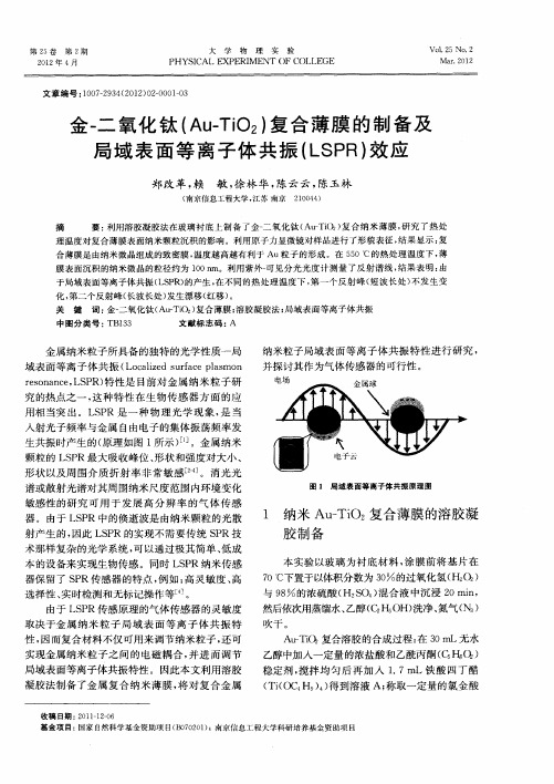
复合阴极Ag/LiF/Al对P3HT:PCBM太阳能电池性能的影响

子 体 共 振 能 随 LF层 厚 度 增 加 , 耗 散 到 铝 膜 上 的共 振 能 量 i 其
同厚度 IF层后 的复合薄 膜的消 光光谱 。IF厚 度增加 ,银 | 』
复合 阴极 Ag L F A 对 P HT: C M 太 阳能 电池 性 能 的影 响 / i/ I 3 PB
周建 萍 ,陈晓红 , 徐
1 .上海电力学院电力 与 自动化工程学院 , 海 上 20 9 000
征。
2 华东师范大学物理系和纳光 电集成与先进装备教育部工程研究 中心 , 。 上海 3 北京交通大学发 光与光信息技术教育部重点实验室, . 北京 1 0 4 004
50 0 6 0 0 W a ee g h n v ln t/ m 70 0
浓度为 2 g・ 的溶液 。P HT : C M 混合 溶液被旋 0r mL n 3 PB
涂到 P D T: S E O P S层上形成 10n/厚的 薄膜 , 后在 10 3 F l 然 2 ℃下退 火 1 i。最后 , 真空镀膜机 中蒸镀 上银 、LF和 5r n a 在 i A, l 真空腔体基体气压为 5 0 or P C电池 面积 为 0 1 ×1 ~ T r。 S . c2 3 r 。P HT: C M 混合 薄膜 的制 备过 程 以及 电池测 试 过 n PB 程都在空气 中进行 。在大气气氛和 AM1 5 0 . G 10mW ・ m c 模 拟太 阳光 下测试 聚合物太 阳能 电池的 电流 电压特性 曲线 。
LF / 8 1 a dAg / i4 A1 ( ) eete u es e oea e— i1A1 ( ) n 4 LF / 8 2 wh r h mb r n t vr n d
等离子体材料及其应用研究

等离子体材料及其应用研究一、引言等离子体材料是指通过激光、光子、电子、离子、等粒子作用下形成的在电子、离子、原子和分子等粒子组成的高度激发态物质。
作为新型材料领域的新星,等离子体材料已经在多个领域得到了应用。
二、等离子体材料的种类1. 等离子体材料的分类根据材料组成,等离子体材料主要可分为单元素等离子体材料、合金等离子体材料和复合等离子体材料等三类。
2. 单元素等离子体材料单元素等离子体材料是由单一元素形成的等离子体材料。
常见的单元素等离子体材料有石墨、碳纳米管、氧化铝、钨等。
3. 合金等离子体材料合金等离子体材料指的是由两种或两种以上的元素组成的等离子体材料。
根据合金成分的不同,合金等离子体材料可分为两类:混合合金等离子体材料和化合物合金等离子体材料。
4. 复合等离子体材料复合等离子体材料是指由两种及以上材料组成的等离子体材料。
常见的复合等离子体材料有金属基复合材料、陶瓷基复合材料和高分子基复合材料等。
三、等离子体材料的应用1. 等离子体材料在半导体领域的应用等离子体技术是半导体制造中必不可少的工艺之一。
等离子体在半导体器件的制造过程中被广泛应用,比如在硅晶片刻蚀过程中使用CF4等气体等离子体和SF6等气体等离子体。
2. 等离子体材料在航天领域的应用等离子体技术在航天领域中也得到了广泛应用,比如利用等离子体喷流推进技术,可以让航天器在较短的时间内达到更高的速度。
3. 等离子体材料在医学领域的应用等离子体材料也在医学领域中得到了广泛的应用,如等离子体手术刀可以用于微创手术,等离子体消毒机可以有效消除医院内的各种细菌和病毒。
4. 等离子体材料在能源领域的应用等离子体材料也在能源领域中得到了应用,利用等离子体技术可以改善燃烧效果、提高燃烧效率和减少污染等。
四、等离子体材料的展望未来,等离子体材料有望在新型存储材料领域、太阳能电池领域、柔性电子领域、纳米材料领域、生物医学材料领域等领域中得到更广泛的应用。
金-二氧化钛(Au-TiO_2)复合薄膜的制备及局域表面等离子体共振(LSPR)效应
器保 留 了 S R传 感 器 的特点 , 如 : 灵敏 度 、 P 例 高 高
选 择性 、 时 检测 和无 标记操 作 等 。 实 4 ]
由于 L P S R传 感原 理 的气体 传感 器 的灵 敏度 取 决 于金 属 纳 米 粒 子 局 域 表 面 等 离 子 体 共 振 特 性, 因而 复合 材料 不仅 可用来 调 节纳 米粒 子 , 还可
文献标志码 : A 中 图分 类 号 : B 3 T 13
金属 纳米 粒子 所具 备 的独特 的光 学性 质一 局
纳米粒 子局 域表 面等 离 子 体 共 振特 性 进 行 研 究 , 并 探讨 其作 为气 体传 感器 的可行 性 。
域 表 面等离 子 体共 振 ( oaie ufc ls n L cl dsraepamo z
rsn n e L P 特性是 目前 对 金 属纳 米 粒 子 研 eo a c , S R)
究 的热点 之一 , 种 特 性 在 生 物传 感 器 方 面 的应 这
用 相 当突 出 。L P 是 一 种 物 理 光 学 现象 , 当 SR 是
入射 光子频 率 与金 属 自由电子 的集体 振荡 频率 发
生 共 振时产 生 的 ( 理 如 图 1 原 所示 )1。金 属纳 米 [ ] 颗粒的 I P R最 大吸 收峰位 、 状 和强度 对 大小 、 S 形
形 状 以及 周 围 介 质折 射 率 非 常 敏感 [ ] 2 。消 光 光
谱 或 散射 光谱 对其 周 围纳米 尺度 范 围 内环 境 变化
局域表面等离子体共振特性 。因此本文利用溶胶
凝 胶 法制 备 了金 属 复合 纳米 薄膜 , 对 复合 金 属 将
金属纳米结构表面等离子体共振及其应用

科技与创新┃Science and Technology&Innovation ·140·2019年第21期文章编号:2095-6835(2019)21-0140-02金属纳米结构表面等离子体共振及其应用*邓英(湖南城市学院,湖南益阳413000)摘要:介绍了纳米光子器件以及金属纳米结构表面等离子体共振,分析了金属纳米结构表面等离子体共振的运用领域,包括在生物医学领域的运用、在局域场增强和拉曼信号检测的运用、在金属纳米颗粒等离子体共振模式检测以及电磁特异介质运用,为金属纳米研究以及运用提供了一定的参考意见。
关键词:纳米光子器件;金属纳米结构;等离子体共振;应用领域中图分类号:TB383.1文献标识码:A DOI:10.15913/ki.kjycx.2019.21.060纳米光子学是材料科学、纳米科学、光物理学、光学工程等多门科学融合之下的一门新科学,目前国际上相关机构正在积极加强对其的有效研究,探究光的产生、传播、转换、调制以及探测等多个领域,电磁特异介质与表面等离子体光学是其中的重要研究分支之一。
1金属纳米结构表面等离子体共振1.1纳米光子器件与传统电子学器件相比,电子学器件具有显而易见的优势,包括传感、成像、光辐射、探测等层面,体积较小,具有较高的集成度以及较快的速度,同时其能耗也较低。
在实际运用过程中,要求光学/光电子器件具有更为强大的功能,探索其与微电子学器件集成之路,在这一基础上研究具有宽频带、大容量、极高速的终端消费产品,以及超小型光电子器件/系统,这是目前信息技术的重要研究方向,为微电子芯片以及光纤通讯之间的研究提供了方向。
1.2金属纳米结构表面等离子体共振目前纳米科学、光物理学等学科研究过程中正在积极加强对表面等离子体光学(plasmonics)结构以及器件的研究,以此实现对纳米尺度的有效操控与控制,为纳米光子学器件的研究提供了新的方向。
在金属的表面以及内部具有大量的自由电子,构成了自由电子气团,即等离子体(plasmon)。
等离子体技术在材料表面改性中的应用研究
等离子体技术在材料表面改性中的应用研究随着人们对材料特性的要求越来越高,材料表面改性技术也越来越受到关注。
而等离子体技术作为一种高效、可控、环保的表面改性方法,近年来受到了广泛关注,并在材料表面改性中得到了广泛应用。
一、等离子体技术概述等离子体(plasma)是一种带电粒子和自由电子的气体状态,具有高能量和高反应活性。
等离子体技术是指利用等离子体对材料表面进行离子轰击、表面化学反应、离子注入等处理,从而改变材料表面特性的方法。
二、等离子体技术在材料表面改性中的应用2.1 表面清洗材料表面清洗是材料表面改性前必要的一步。
等离子体技术可用于表面清洗,其离子轰击能够有效地去除表面杂质和氧化物,提高表面纯度和清洁度。
2.2 表面硬化利用等离子体处理能够使材料表面硬度增加几倍甚至几十倍,提高材料的耐磨性和耐蚀性。
这是因为等离子体处理过程中产生的活性粒子高速撞击材料表面,使其表面发生塑性变形和冷变形,形成了高密度的晶界,进而提高了材料表面的硬度和强度。
2.3 表面涂层等离子体技术还可以应用于表面涂层。
利用等离子体处理可以改善物质的表面亲和力和等离子体处理过程中产生的活性粒子可用于表面化学反应,使得表面涂层更加牢固耐用。
2.4 表面改性等离子体技术还可用于材料表面的化学修饰,例如通过等离子体轰击和离子注入等方式,使得表面分子结构或化学结构发生变化,从而改变表面的性质和功能。
三、等离子体技术的优点和不足3.1 优点(1) 高效:等离子体技术处理速度快,一个相对较小的样品可以在几秒钟内得到处理;(2) 可控性强:可以调节等离子体的电场、功率、成分等参数,控制等离子体处理的深度、速度和质量;(3) 环保:等离子体技术不需要使用有机溶剂和腐蚀性酸碱等物质,对环境的污染小,有助于环保。
3.2 不足(1) 昂贵:等离子体处理设备的购买和维护成本较高;(2) 设备复杂性高:等离子体处理设备需要高压电源和气体供应等支持,对处理条件有较高的要求,操作难度较大。
基于表面等离子体的金属-非线性介质复合结构的全光调制
Jn 02 u .2 1
基 于表 面等 离子 体 的金属 一非 线性 介 质 复 合 结 构 的 全 光 调 制
邓 燕 , 刘 果 红
( 安徽建筑2 业学院 数理 系, 1 2 合肥 200) 3 6 1
摘
要: 针对传统的全光调制器件 , 出了一种在金属 一非线性 介质复合 结构 中基 于表 面等离子体 的高灵敏 提
Ab ta t I o a io t h r d t n l alo t a d l t r a n w i h s n ii e l w u p sr c :n c mp rs n wih t e t a ii a l p i lmo u a o , e h g e stv , o p m o — c
l h n e st r h wn t h n et en n ie rr fa t eid x o o l e rd ee ti ,wh c a i tit n iywe es o o c a g h o l a e rc i e fn n i a ilcrc g n v n n ih m y b u fce ty lr et n l e tt er s n n ec n iin o u fc ls o o e .Th s h l o t— es fiin l a g oi f n h e o a c o dt fs ra ep a m nm d s u o u ,t eal p i - c lmo ua in wa b an d a d lto so tie .
传 统 的光调 制器 大部分 利用 光致变 色材 料来 实现 光 控光 的全 光调 制 , 为 光致 变 色 材 料 的偶 氮 聚 作
制的效果 , 制约 了调制速度等 因素 的提高。随着 近年来微 纳 加工 技 术 和集 成 光 学 的发 展 , 究 者 研 们发现利用纳米光子学 中表面等离子体激元 的特
金属纳米结构表面等离子共振及应用

金属纳米结构表面等离子共振及应用刘海露;陈旭东【摘要】金属纳米结构表面等离子共振具有特殊的光学性质并且可以以一些非常独特的方式来操纵光波,在物理、化学、医药、生物、环境等领域有着广泛的应用.本文简单介绍了等离子共振的概念,分别从基础理论研究、仿真计算及应用研究三方面来概述表面等离子共振,并就其在现代光子学和光信息技术的发展方向作了展望.【期刊名称】《合成材料老化与应用》【年(卷),期】2018(047)005【总页数】7页(P100-105,121)【关键词】金属纳米结构;制备;表面等离激元;应用【作者】刘海露;陈旭东【作者单位】中山大学化学学院,广东广州510275;中山大学化学学院,广东广州510275【正文语种】中文【中图分类】O6-1当光波入射到金属材料表面时,光和金属纳米颗粒中电子的相互作用能够增强电子的集体振动,如果电子振动频率与入射波的频率一致,外界光场就会被集体振动的电子俘获,使得金属材料表面自由电子与外界光电子耦合形成一种特殊的电磁模式。
共振电磁波作为在微纳尺度下进行光子操纵和集成的优良载体,可利用其过程中纳米金属表面能量转移、等离子体共振能量转移、金属增强发光等特性来研究表面等离激元现象,近年来该领域在实验和理论方面都取得了很大的进展,相关学术研究成果陆续在国际顶尖刊物上发表[1-5]。
本文将分别从基础理论研究、仿真计算及应用研究三方面来概述表面等离子共振,并就其发展方向作了展望。
1 基础理论研究金属纳米粒子组成、形态、尺寸及分布、表面形貌和表面电子结构,纳米阵列结构等对聚合物表面等离激元共振效应有着重要的影响,且不同厚度、不同形状的隔离层微结构对表面等离激元的调制效果也不同。
目前研究主要集中在如下五个方面。
1.1 金属纳米结构构建方法金属纳米结构的构建方法大致分为两类,即化学法(氧化还原法、模板法、电化学法等)和物理法(真空蒸镀法、等离子体溅射法等)。
金、银纳米材料由于合成方法简单、化学性能稳定、独特的光学性质成为最受欢迎的基材。
半导体 -金属杂化纳米

半导体 -金属杂化纳米
半导体-金属杂化纳米结构是指将半导体材料与金属材料结合在一起,形成纳米尺度的复合材料。
这种杂化结构通常具有以下特点和应用:
1. 协同效应:半导体和金属的结合可以产生协同效应,如电荷转移、界面等离子体共振等,从而增强材料的电子、光学和催化性能。
2. 电荷分离:在半导体-金属杂化纳米结构中,电荷可以从半导体转移到金属,或者相反,这种电荷分离可以用于提高光电转换效率。
3. 表面等离子体共振(SPR):金属纳米颗粒在特定波长的光照射下会产生SPR现象,这可以用于增强光电探测器和生物传感器的灵敏度。
4. 催化性能:半导体-金属杂化纳米结构通常具有优异的催化性能,可以用于催化反应,如光催化、电催化等。
5. 光学性能:这种杂化结构可以调节光的吸收、发射和散射,因此可以用于光电子器件、光开关和光调制器等。
6. 电子性能:半导体的引入可以调节金属的电子性能,如改变其功函数、电导率等。
7. 热电性能:半导体-金属杂化纳米结构可以用于热电发电和制冷,因为它们具有良好的热电性能。
8. 能源存储与转换:这种杂化结构可以用作超级电容器、电池和太阳能电池等能源存储与转换设备的电极材料。
9. 环境监测与治理:半导体-金属杂化纳米结构可以用于水处理、
气体传感和污染物降解等环境监测与治理应用。
10. 生物医药:在生物医药领域,这种杂化结构可以用作药物递送系统、生物成像和生物传感器等。
半导体-金属杂化纳米结构的研究和开发是纳米科技领域的前沿方向,它们在许多高科技领域都有着广泛的应用前景。
金纳米颗粒在等离子体共振光催化剂中的作用机理研究

金纳米颗粒在等离子体共振光催化剂中的作用机理研究曹寅虎;曹溢涛;吴骊珠;佟振合;张铁锐【摘要】金纳米颗粒在等离子体共振光催化剂中具有多种不同的作用机理.本文采用溶胶-凝胶法合成了氮/碳共掺杂超薄二氧化钛(D-TiO2)包覆的SiO2/Au/D-TiO2三明治型及SiO2/D-TiO2核壳纳米结构材料,对金纳米颗粒在含有可见光响应型半导体的等离子体共振光催化剂光催化分解水制氢反应中的作用机理进行了探索.研究结果表明,在该等离子体共振光催化剂的光催化反应过程中,金纳米颗粒同时体现出肖特基效应和等离子体共振效应作用机理,且作用机理与光生载流子的多少以及金纳米颗粒的负载量有关.负载量较低时,金纳米颗粒的作用机理与光生载流子的多少有关.而在高负载量条件下,金纳米颗粒在可见光照射下主要表现出肖特基效应对光催化活性的影响.【期刊名称】《影像科学与光化学》【年(卷),期】2015(033)005【总页数】9页(P394-402)【关键词】金纳米颗粒;等离子体共振光催化剂;光催化制氢;作用机理【作者】曹寅虎;曹溢涛;吴骊珠;佟振合;张铁锐【作者单位】中国科学院理化技术研究所,北京100190;中国科学院大学,北京100049;中国科学院理化技术研究所,北京100190;中国科学院大学,北京100049;中国科学院理化技术研究所,北京100190;中国科学院理化技术研究所,北京100190;中国科学院理化技术研究所,北京100190【正文语种】中文21世纪以来,能源短缺和环境污染逐渐成为阻碍人类发展的两个亟需解决的问题[1-5]。
利用太阳能光催化制氢被认为是解决能源和环境问题的理想途径之一,因此,高效光催化剂的研发受到了国内外科学家的高度关注[6-13]。
尽管光催化剂的研究已经取得了显著进展,但光催化剂在能源和环境方面的大规模应用仍受到很大限制。
其中一个主要的原因就是半导体材料中光生电子和空穴较高的复合几率使得半导体光催化剂的催化效率普遍较低[14-17]。
等离子体技术在新型材料加工中的应用

等离子体技术在新型材料加工中的应用随着现代科技的发展和创新,新型材料加工技术也在不断提高和改进。
其中一种重要的技术就是等离子体技术。
利用等离子体技术,可以对材料进行高密度、高空间分辨率的精细加工,这为新型材料的制备和研究开辟了新的道路。
一、等离子体技术的基本原理等离子体是一种高度激发态的物质,是由多种带电粒子组成的气体。
在等离子体技术中,利用电场或者电子束激发气体,使其电离,产生的带电粒子受电磁场共同作用,变成一个大量自由电子和离子体系统。
这种离子体体系具有高度的热力学稳定性,在等离子体的物理特性中,包括电子温度、离子温度、电子密度、离子密度、等离子体密度和等离子体成分等方面都有特殊的物理规律。
二、等离子体技术在新型材料加工中的应用(一)等离子体刻蚀技术等离子体刻蚀技术是利用等离子体反应动力学原理,使材料表面受到氟离子的作用,使其分子间键断裂,从而达到对材料进行精细加工的目的。
这种加工方式具有高精度、低损伤和高速度等特点,特别适用于硅、氮化硅、氮代硅等新型材料的制备和加工。
(二)等离子体沉积技术等离子体沉积技术是将气体通过等离子体激发后,产生的反应产物沉积到材料表面上,从而改善材料的性能。
这种技术可用于制备金属、氧化物、二硫化钼和氮化硅等材料。
在新型材料的制备中,等离子体沉积技术被广泛应用,可以制备出高质量、低损伤的薄膜。
(三)等离子体烧结技术等离子体烧结技术是利用等离子体所产生的高温高能离子束,将材料表面与气相物质快速反应,从而将材料表面熔化或达到高度结晶状态,进而实现材料烧结和合成等目的。
这种技术可用于制备尖晶石、氮化硅等复合材料,也可以用于制备晶体管、发光器件等电子元器件。
三、等离子体技术在材料工业领域的发展前景等离子体技术已经成为了新型材料加工中的重要手段,它具有高效、环保、低成本的特点。
未来,等离子体技术将会更广泛应用,在纳米材料、生物医学材料、新能源材料等领域都将发挥独特的优势。
等离子体技术的发展也将带动新型材料的制备和应用,推动科技创新和产业革命。
金属纳米材料表面等离子共振吸收的表征及其应用

627
657
410
618
407
405
541
539
557
H2O, n=1.333 EtOH, n=1.361
DMF, n=1.426
80(蓝色)和60nm(红色)的Ag纳米棱柱在不同介质中的UV-vis光谱
插图是Ag纳米球相应的光谱
Pastoriza-Santos, I., Nano Lett., 2002, 2, 903 Pastoriza-Santos, I., Langmuir, 2002, 18, 2888
金椭圆体
aspect ratio 1.94 2.35 2.48 3.08
金球
金纳米棒
顶部: 计算的紫外可见吸收光谱 底部: 实验的光谱
Au vol% 10 30 50 60 70
金薄膜
separation/nm
∞
15 7.5 1.5 1 0
多层金薄膜
Luis M., Langmuir, 2006, 22, 32
N+ C
N+ C
97nm 57nm 40nm 23nm 14nm 6nm
97nm
57nm 40nm 23nm 14nm 6nm
10-4M的PDI在不同直径的Au纳米粒子上的SERS谱图
Chung-ro Lee, J. Colloid Interface Sci., 2004, 271, 41
SPR检测原理
50000 0 0
5000 4000 3000 2000 1000
0 012345
100 80 60 40
20
5
10
15
Na的研究进展-纳米化学, 300
a. r. : 2.61 a. r. : 2.94 a. r. : 3.31
微纳传感器复合结构的综述
微纳传感器复合结构的综述摘要:传感技术一直是当今科学界研究的热点问题。
传统的传感器体型大,操作流程复杂,而且价格高昂,不易携带,耗时耗力。
为了有效地改善这一问题,科学家们提出了金属-介质复合纳米结构并且把这种结构应用于传感器中。
随着人们对该结构的研究的深入,金属-介质复合纳米结构传感器将会广泛的应用在越来越多的领域。
本文主要从金属-介质复合纳米结构的分类和应用两个方面对该结构的研究和发展进行综述。
关键词:微纳传感器、金属复合纳米结构一、金属-介质复合纳米结构的分类1.1 贵金属复合纳米结构最早研究的单一金属材料不具备足够的稳定性,所以引进了多种不同的金属材料组成复合结构。
经过研究表明多种金属材料复合结构可以同时拥有两种或多种组成金属的化学性质,甚至可能会由于协同作用而具有更优的性质。
因为贵金属纳米颗粒具有LSPR效应,可以对光有很强的吸收作用,所以贵金属纳米颗粒可以灵敏的捕捉到其周围环境的折射率[1]。
这种性质可以被应用于局域表面等离子体传感技术中[2]。
1.2 金属-电介质材料复合纳米结构随着科学家们的进一步研究,发现贵金属复合材料的化学稳定性较差以及成本较高,为了避免这些缺点,考虑在复合结构中加入非金属材料起辅助功能,实验表明金属材料和电介质材料合理的复合结构可以表现出比单一纯金属结构更好的光学性质。
1.3 金属-导体复合纳米结构导体材料因为具有优良的导电性和相容性,所以被广泛的应用到传感器的研究中。
科学家们想到了把石墨烯这种导体材料和金属材料结合形成新的复合结构。
这是因为石墨烯具有极大的比表面积、柔韧性和极强的吸附能力,可以作为与金属纳米材料结合形成复合结构的支撑材料,很好的避免了金属纳米结构本身的团聚,从而保持较大的表面积和良好的化学性质[3]。
这一特性可以完美的应用于SPR检测传感器中,提高SPR传感器的稳定性和灵敏度[4]。
1.4 金属-半导体复合纳米结构金属-半导体组成的复合纳米结构与其对应的单体相比具有灵敏度高、响应速度快、便于智能化等独特的性能,所以金属-半导体复合纳米材料可以应用于非线性光电子器件的设计领域[5]。
- 1、下载文档前请自行甄别文档内容的完整性,平台不提供额外的编辑、内容补充、找答案等附加服务。
- 2、"仅部分预览"的文档,不可在线预览部分如存在完整性等问题,可反馈申请退款(可完整预览的文档不适用该条件!)。
- 3、如文档侵犯您的权益,请联系客服反馈,我们会尽快为您处理(人工客服工作时间:9:00-18:30)。
LSPR——dielectric environment——sensing techniques
The electrons are free to move in one or two dimensions, thus SPPs
can be excited and propagate along the metal/dielectric interface.
NWs/NWs
2、Coupled medal NPs
NPs dimers and “hot spots”
The influencing factors of the near field coupling
1、Angle——the incident electric field∥the axis (Max) 2、 Gap——gap↓——energy↓——resonance peak
Heterodimer——novel optical properties ———Fano resonance.
EM coupling( non-spherical )—— relative orientation.
The nanogaps which strongly confine induced EM fields are supreme systems for SERS applications
等离子体(成分的
物质形态,广泛存在于宇宙中,常被视为是物质的第四态,被称为等离 子态,或者“超气态”,也称“电浆体”。
等离子体的特性
1、具有很高的电导率,和电磁场的耦合作用也极强 2、和一般气体不同,包含两到三种不同的组成粒子,且组成粒子间的相互 作用较大 3、速率分布可能偏离麦克斯韦分布 4、具有表面等离效应
Based on the SPs interference principle, a complete set of plamonic logic gates and other functional devices can be realized by designing different NW networks
LSPR is altered
the interaction —— the distance
The EM coupling between the NP and the image particle produce large field enhancement in the gap between the NP and the film
nanohole NPs arrays
single molecule SERS
plasmonic antennas
nanohole/NP pairs plasmonic tweezers nanocube dimers quantum plasmonics nanorod dimers nonlinear plasmonics
SPP characteristics in metal NWs
Applications
4、NWs network structures
4.1 SPP routing in branched NWs
4.2 SPP interference in complex NWs network
1、The thickness of the film is much larger than the diameter of the NP 2、The film can then be treated as a mirror
3.2 Coupled NPs/NWs
Characteristic of NWs
6 Conclusion
In complex metal nanostructures, the SPs in each single component interact with that in the others, for example, LSPs in a single NP can couple to that in another one or to SPPs in a NW or metal film,resulting in extra EM enhancement at the nanogaps. SPPs in different NWs can interfere with each other, making possible selective routing of propagating SPPs to desired output terminals. The complex EM interactions give rise to more flexibility in tailoring the SPs for advanced applications, such as remote SERS sensing and plasmonic logic gates. The dielectric substrate or surface coating is another critical parameter that affects the SPs properties, including the LSPR and the SPPs wavelength and propagation length. In fact, this effect provides an alternative method to tailor the SPs characteristics for particular applications.
the plasmonic properties of several typical types of complex metal nanostructures
electromagnetically coupled nanoparticles NPs/metal films NPs/nanowires (NWs)
报告人:
Content
1、introduction of plasma
2、coupled metal NPs 3、coupled NPs/metal film and NPs/NWs 4、NWs network structures 5、Conclusion
1、 introduction of plasma
等离子体的应用:工业、农业、环保、军事、宇航、能源、天体等方面
In metal nanoparticles , the collective oscillations of free electrons
are confined in all three-dimensions, resulting in the reputed localized surface plasmons (LSPs).
3、Coupled NPs/metal film and NPs/NWs
3.1 NP over metal film (NPOF)
A dipole ——an image dipole ( incident electric field
⊥surface)
The system: the NP →the image