RS485抗干扰电路设计
RS485串行通信电路设计

RS485串行通信电路设计RS485是一种常见的串行通信协议,广泛应用于工业自动化、仪器仪表、电力系统等领域。
RS485通信具有高可靠性、抗干扰能力强、通信距离远等特点,因此在一些需要长距离、高可靠性的通信场景中得到广泛应用。
本文将针对RS485串行通信电路的设计进行详细介绍。
首先,我们需要了解RS485通信的基本原理。
RS485采用差分信号传输,即发送端将逻辑0和逻辑1分别表示为低电平和高电平,接收端通过比较接收到的两个信号的电平差值来判断传输的是0还是1、差分信号传输具有较强的抗干扰能力,可以有效地抵抗电磁干扰和串扰。
除了收发芯片,RS485通信电路还需要考虑其他一些因素。
首先是电源电压的选择,一般RS485通信电路的电源电压为5V,但也可以根据实际需求选择其他电压。
其次是控制信号的设计,通常需要使用一个使能信号来控制发送和接收的开关。
此外,还要考虑阻抗匹配和信号线的布线,通常使用120欧姆电阻进行阻抗匹配,并尽量避免信号线与电源线、高电压线等干扰源的靠近。
在实际设计中,我们可以参考以下步骤进行RS485串行通信电路的设计:1.确定通信距离和通信速率:根据实际需求确定通信的最远距离和传输速率,这将影响到电路设计的一些参数。
2.选择收发芯片:根据通信距离和速率的要求,选择合适的收发芯片,并根据其规格书进行电路连接和布线。
3.设计电源电路:确定电源电压和电流,并设计相应的电源电路,通常需要增加滤波电容来提高电源的稳定性。
4.控制信号设计:根据收发芯片的要求设计使能信号和其他控制信号的接口电路。
5.阻抗匹配和信号线布线:根据通信距离和速率要求,选择合适的阻抗匹配电阻,并良好地布线,以减少干扰和串扰。
6.电路测试和优化:完成电路设计后,进行测试和优化,检查通信稳定性和可靠性,并根据需要进行一些调整和改进。
总之,RS485串行通信电路设计是一个相对复杂的过程,需要考虑多个因素的综合。
通过仔细设计和优化,可以实现稳定、可靠的串行通信。
光电隔离RS485典型电路
光电隔离RS485典型电路一、RS485总线介绍RS485总线是一种常见的串行总线标准,采用平衡发送与差分接收的方式,因此具有抑制共模干扰的能力。
在一些要求通信距离为几十米到上千米的时候,RS485总线是一种应用最为广泛的总线。
而且在多节点的工作系统中也有着广泛的应用。
二、RS485总线典型电路介绍RS485电路总体上可以分为隔离型与非隔离型。
隔离型比非隔离型在抗干扰、系统稳定性等方面都有更出色的表现,但有一些场合也可以用非隔离型。
我们就先讲一下非隔离型的典型电路,非隔离型的电路非常简单,只需一个RS485芯片直接与MCU的串行通讯口和一个I/O控制口连接就可以。
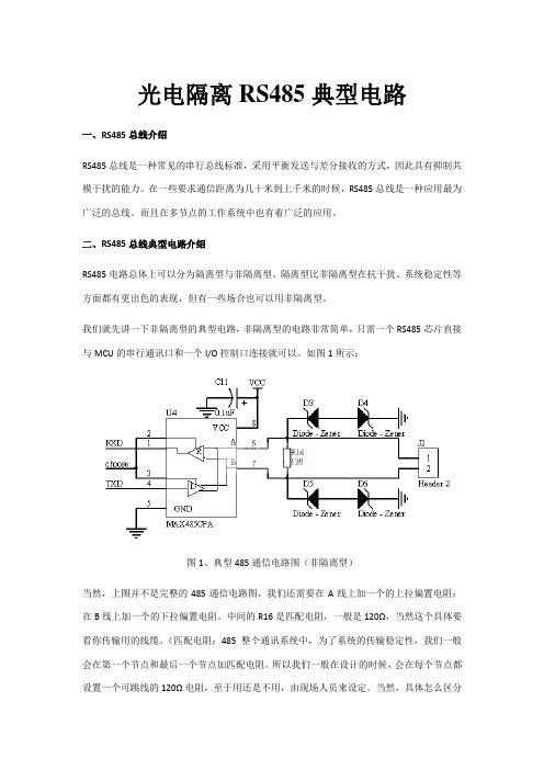
如图1所示:图1、典型485通信电路图(非隔离型)当然,上图并不是完整的485通信电路图,我们还需要在A线上加一个的上拉偏置电阻;在B线上加一个的下拉偏置电阻。
中间的R16是匹配电阻,一般是120Ω,当然这个具体要看你传输用的线缆。
(匹配电阻:485整个通讯系统中,为了系统的传输稳定性,我们一般会在第一个节点和最后一个节点加匹配电阻。
所以我们一般在设计的时候,会在每个节点都设置一个可跳线的120Ω电阻,至于用还是不用,由现场人员来设定。
当然,具体怎么区分第一个节点还是最后一个节点,还得有待现场的专家们来解答呵。
)TVS我们一般选用的,这个我们会在后面进一步的讲解。
RS-485标准定义信号阈值的上下限为±200mV。
即当A-B>200mV时,总线状态应表示为“1”;当A-B<-200mV时,总线状态应表示为“0”。
但当A-B在±200mV之间时,则总线状态为不确定,所以我们会在A、B线上面设上、下拉电阻,以尽量避免这种不确定状态。
三、隔离型RS485总线典型电路介绍在某些工业控制领域,由于现场情况十分复杂,各个节点之间存在很高的共模电压。
虽然RS-485接口采用的是差分传输方式,具有一定的抗共模干扰的能力,但当共模电压超过RS-485接收器的极限接收电压,即大于+12V或小于-7V时,接收器就再也无**常工作了,严重时甚至会烧毁芯片和仪器设备。
RS-485总线故障保护偏置技术提高抗干扰的应用研究
RS-485总线故障保护偏置技术提高抗干扰的应用研究发布时间:2023-02-01T08:18:39.079Z 来源:《中国科技信息》2022年9月第18期作者:赵震[导读] 通信技术近年来快速发展。
RS-485作为一种成熟的通信技术由于成本低赵震广东美控智慧建筑有限公司摘要:通信技术近年来快速发展。
RS-485作为一种成熟的通信技术由于成本低,接线方便等优点广泛应用于工业控制、楼宇自控等领域。
但由于485通信电路简单,使用环境干扰大,再加上外围抗干扰电路设计不当,会造成485电路无法正常通信。
通过485总线故障保护偏置技术,可以较好的提485的高抗干扰能力。
引言:随着电子技术的快速发展以及自动化控制的在各行各业的广泛应用,通信技术在控制设备间数据交互,网络组建,远程控制等起着不可替代的作用。
RS-485通信作为较早出现,且应用成熟的一种通信技术,因其成本低,接线方便,易维护等优点,仍广泛应用于工业控制、楼宇自控等各个领域。
但由于485通信出现时间较早,外围电路设计简单,再加上通信距离长,且使用环境存在各大功率电机、变频器等强干扰设备,对485通信产生较大的干扰,若485通信电路抗干扰电路设计不当,会造成485电路通信丢包率加大,甚至无法正常通信,从而影响自动化设备的正常工作。
一、常见RS-485抗干扰方法介绍RS-485通信在多年的应用中,工程师们积累了大量的提高485抗干扰的方法和手段,为RS-485通信的稳定性做出了巨大的贡献。
总结有如下几类:1.总线故障保护偏置技术,是一种常用的一种提高485抗干扰的重要方法。
通常在RS-458总线增加偏置电阻。
来提高抗干扰能力。
2.终端匹配电阻:通信线过长时,通过在485总线上增加120Ω的终端匹配电阻,来吸收电压反射信号。
3.总线串联电阻、电感或磁珠滤除高频干扰,提高通信质量。
4.采用更新型的RS-485芯片:优化后的RS-485接收器的门限电平VIT+降低,例如MAX13085芯片的收门限电平VIT+为-50mV的门限电平,可以避免总线空闲时总线为0V处于不确定状态。
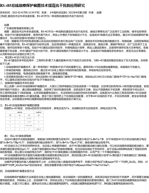
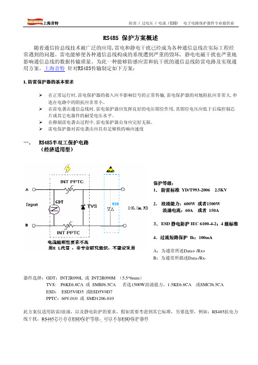
485保护电路
PTC起限流隔离退耦作用,根据大量浪涌测试验证选取10欧姆左右的JK250-120u,表贴式为mSMD010-1812. TVS二极管的选取为SMBJ6.5CA-TP
防护设计原理:RS485总线的分级防护电路图,当雷击发生时,感应过电压由两端引入,GDT 气体放电管做一级防护,此时过电压被大大削弱到数百伏左右,再经过PPTC限流,TVS二极管做二次限压,使到后端电路的电压被箝制在8V左右,从而实现对后端电路的保护。
TVS2/3做共模保护,TVS1做差模保护。
保护等级:可通过IEC61000-4-5,4级标准:1.2/50us 4KV 、10/700us 6KV
现在我们的方案是2个TED485, 2个250-120的PTC, 一个SM712, adum2483, bs0505隔离电源, 这个方案倒是2年多一直都没发生过烧芯片的事情.
1)PTC元件和被保护电路串联连接,当电路中的电流迅速增加时,PTC的电阻迅速增加,从而限制电路过电流,实现对被保护对象的保护。
mSMD010-1812的最大工作电压是60V。
2)信号接口的浪涌防护需要做共模、差模的防护。
气体放电管如是玻璃气体放电管,则需要使用3只,如三端陶瓷气体放电管,则使用一只。
3)TVS具有的另一个优点是可灵活选用单向或双向保护器件,在单极性的信号电路和直流电源电路中,选用单向TVS管。
反之则选择双向。
4)电子系统来说, “地”可以分为两种: 一种是“大地”, 另一种是“工作基准地”, 实践证明, 良好地接地可以在很大程度上抑制系统内部噪声耦合, 防止外部干扰地侵入, 提高系统地抗干扰能力。
防雷保护接地是接大地。
机械自动化控制系统中RS485接口电路设计
机械自动化控制系统中RS485接口电路设计摘要:机械自动化控制系统的控制端采用RS485总线方式。
RS485作为一种传统工业总线,在工业控制上有广泛的应用。
RS485的接口信号与TTL电平兼容,可方便与TTL电路连接。
RS485采用平衡驱动器和差分接收器的组合,抗共模干扰能力增强,具有良好的抗噪声干扰性。
RS485最大的通信距离约为1219m,最大传输速率为10Mb/S,传输速率与传输距离成反比,RS485总线允许连接多达128个收发器,上述优点就使其成为首选的串行接口。
因此,本文对机械自动化控制系统中RS485接口电路设计做出研究。
关键词:机械自动化控制系统RS485接口电路设计在机械自动化控制系统的研究与开发中,控制机采用RS485总线方式进行通信,其设计与开发主要完成将控制端的RS485通信方式转换成光通信方式,将光通信方式转换成执行端的CAN总线方式即完成RS485总线转光和光转CAN 移线模块的设计与开发。
因此,本文对RS485接口电路设计做出分析。
RS485是在RS422基础上发展来的。
在RS422中定义了一种平衡通信接口,将传输速率提高到10Mbps,传输距离延长到400英尺(速度低于100kbps时),并允许在一条平衡线上连接最多10个接收器。
RS422是一种单机发送,多机接收的单向、平衡传输规范标准。
为了扩展应用范围,在RS422标准的基础上,1983年EIA研究出了一种支持多节点、远=距离和接收高灵敏度的RS485总线标准,该标准增加了多点、双向通信能力,即允许多个发送器连接到同一总线上。
同时,增加了发送器的驱动能力冲突保护特性,扩展了总线的共模范围。
RS485支持半双工或全双工模式,网络拓扑结构一般采用终端匹配的总线型结构,不支持环形或星形网络,最好采用一条总线将各个节点串接起来,从总线到各个节点的引出线长度尽量短,以便使引出线中的反射信号对总线信号影响尽量最低。
一,RS485收发电路设计RS485收发器,采用高速的RS485/RS422收发器MAX3080,MAX3080中内部集成了一个接收器,一个发送器。
RS485电路参考设计
Application ReportSLLA272B–February2008–Revised May2008The RS-485Design Guide Thomas Kugelstadt HPL-InterfaceABSTRACTAs a short compendium for successful data transmission design,this application reportdiscusses the important aspects of the RS-485standard.IntroductionIn1983,the Electronics Industries Association(EIA)approved a new balanced transmission standardcalled RS-485.Finding widespread acceptance and usage in industrial,medical,and consumerapplications,RS-485has become the industry’s interface workhorse.This application report presents design guidelines for engineers new to the RS-485standard that can help them accomplish a robust and reliable data transmission design in the shortest time possible.In a comprehensive way,this document discusses the important aspects of the RS-485standard byfocusing on the following subjects:bus topology,signal levels,cable type,bus termination,failsafe,bus loading,data rate versus bus length,minimum node spacing,and grounding and isolation.Standard and FeaturesRS-485is an electrical-only standard.In contrast to complete interface standards,which define thefunctional,mechanical,and electrical specifications,RS-485only defines the electrical characteristics of drivers and receivers that could be used to implement a balanced multipoint transmission line.This standard,however,is intended to be referenced by higher level standards,such as DL/T645,forexample,which defines the communication protocol for electronic energy-meters in China,specifyingRS-485as the physical layer standard.Key features of RS-485are:•Balanced interface•Multipoint operation from a single5-V supply•–7-V to+12-V bus common-mode range•Up to32unit loads•10-Mbps maximum data rate(at40feet)•4000-foot maximum cable length(at100kbps)Network TopologyThe RS-485standards suggests that its nodes be networked in a daisy-chain,also known as party line or bus topology(see Figure1).In this topology,the participating drivers,receivers,and transceivers connect to a main cable trunk via short network stubs.The interface bus can be designed for full-duplex orhalf-duplex transmission(see Figure2)Figure1.RS-485Bus StructureSLLA272B–February2008–Revised May2008The RS-485Design Guide1 Submit Documentation FeedbackR RT T TR R++VConductorInsulationSheath Cable :Type :Impedance :Capacitance :Velocity :Belden 3109A4-pair,22AWG PLCT /CM 12011pF/ft78% (1.3ns/ft)W Signal Levels The full-duplex implementation requires two signal pairs,(four wires),and full-duplex transceivers withseparate bus access lines for transmitter and receiver.Full-duplex allows a node to simultaneouslytransmit data on one pair while receiving data on the other pair.Figure 2.Full-Duplex and Half-Duplex Bus Structures in RS-485In half-duplex,only one signal pair is used,requiring the driving and receiving of data to occur at different times.Both implementations necessitate the controlled operation of all nodes via direction control signals,such as Driver/Receiver Enable signals,to ensure that only one driver is active on the bus at any time.Having more than one driver accessing the bus at the same time leads to bus contention,which,at alltimes,must be avoided through software control.Signal LevelsRS-485standard conform drivers provide a differential output of a minimum 1.5V across a 54-Ωload,whereas standard conform receivers detect a differential input down to 200mV.The two values provide sufficient margin for a reliable data transmission even under severe signal degradation across the cable and connectors.This robustness is the main reason why RS-485is well suited for long-distancenetworking in noisy environment.Figure 3.RS-485Specified Minimum Bus Signal LevelsCable TypeRS-485applications benefit from differential signaling over twisted-pair cable,because noise from external sources couple equally into both signal lines as common-mode noise,which is rejected by the differential receiver input.Industrial RS-485cables are of the sheathed,unshielded,twisted-pair type,(UTP),with a characteristicimpedance of 120Ωand 22–24AWG.Figure 4shows the cross-section of a four-pair,UTP cable typically used for two full-duplex networks.in two-pair and single-pair versions,are available toaccommodate the low-cost design of half-duplex systems.Figure 4.Example of RS-485Communication Cable2The RS-485Design Guide SLLA272B–February 2008–Revised May 2008Submit Documentation FeedbackR TL Stub v t r10v c(1) Bus Termination and Stub Length Beyond the network cabling,it is mandatory that the layout of printed-circuit boards and the connector pin assignments of RS-485equipment maintain the electrical characteristics of the network by keeping both signal lines close and equidistant to another.Bus Termination and Stub LengthData transmission lines should always be terminated and stubs should be as short as possible to avoid signal reflections on the line.Proper termination requires the matching of the terminating resistors,R T,to the characteristic impedance,Z0,of the transmission cable.Because the RS-485standard recommends cables with Z0=120Ω,the cable trunk is commonly terminated with120-Ωresistors,one at each cable end(see Figure5,left).Figure5.Proper RS-485TerminationsApplications in noisy environments often have the120-Ωresistors replaced by two60-Ω,low-pass filters to provide additional common-mode noise filtering,(see Figure5,right).It is important to match the resistor values,(preferably with1%precision resistors),to ensure equal rolloff frequencies of both rger resistor tolerances,(i.e.,20%),cause the filter corner frequencies to differ and common-mode noise to be converted into differential noise,thus compromising the receiver’s noise immunity.The electrical length of a stub,(the distance between a transceiver and cable trunk),should be shorter than1/10of the driver’s output rise time,and is given through:WhereL Stub=maximum stub length(ft)t r=driver(10/90)rise time(ns)v=signal velocity of the cable as factor of cc=speed of light(9.8×108ft/s).Table1lists the maximum stub lengths of the cable in Figure4,(78%velocity),for various driver risetimes.Table1.Stub Length Versus Rise TimeDEVICE SIGNAL RATE RISE TIME MAXIMUM STUB LENGTH[kbps]tr[ns][ft]SN65HVD1210001007SN65LBC184********SN65HVD3082E20050038 Note:drivers with long rise times are well suited for applications requiring long stub lengths and reduced, device-generated EMI.FailsafeFailsafe operation is a receiver’s ability to assume a determined output state in the absence of an input signal.Three possible causes can lead to the loss of signal(LOS):SLLA272B–February2008–Revised May2008The RS-485Design Guide3 Submit Documentation FeedbackR B+V Bus*minV ABǒ1ń375)4ńZ0Ǔ(2)R T120R B523R BR T523W120WN+32UL STANDARD*20UL FAILSAFEUL per transceiver(3)Bus Loading 1.Open-circuit,caused by a wire break or by the disconnection of a transceiver from the bus2.Short-circuit,caused by an insulation fault connecting the wires of a differential pair to another3.Idle-bus,occurring when none of the bus drivers is active.Because these conditions can cause conventional receivers to assume random output states when the input signal is zero,modern transceiver designs include biasing circuits for open-circuit,short-circuit,and idle-bus failsafe,that force the receiver output to a determined state,under an LOS condition.A drawback of these failsafe designs is their worst-case noise margin of10mV only,thus requiringexternal failsafe circuitry to increase noise margin for applications in noisy environments.An external failsafe circuit consists of a resistive voltage divider that generates sufficient differential bus voltage,to drive the receiver output into a determined state.To ensure sufficient noise margin,V AB must include the maximum differential noise measured in addition to the200-mV receiver input threshold,V AB= 200mV+V Noise.The values for the failsafe bias resistors,R B,are calculated for worst-case conditions,that is,maximum noise at minimum supply:For a minimum bus voltage of4.75V,(5V–5%),V AB=0.25V,and Z0=120Ω,R B yields528Ω.Inserting two523-Ωresistors in series to R T establishes the failsafe circuit shown in Figure6.Figure6.External Idle-Bus Failsafe BiasingBus LoadingBecause a driver's output depends on the current it must supply into a load,adding transceivers andfailsafe circuits to the bus increases the total load current required.To estimate the maximum number of bus loads possible,RS-485specifies a hypothetical term of a unit load(UL),which represents a loadimpedance of approximately12kΩ.Standard-compliant drivers must be able to drive32of these unitloads.Today’s transceivers often provide reduced unit loading,such as1/8UL,thus allowing theconnection of up to256transceivers on the bus.Because failsafe biasing contributes up to20unit loads of bus loading,the maximum number oftransceivers,N,is reduced to:Thus,when using1/8-UL transceivers,it is possible to connect up to a maximum of96devices to the bus. Data Rate Versus Bus LengthThe maximum bus length is limited by the transmission line losses and the signal jitter at a given datarate.Because data reliability sharply decreases for a jitter of10%or more of the baud period,Figure7 shows the cable length versus data rate characteristic of a conventional RS-485cable for a10%signal jitter.4The RS-485Design Guide SLLA272B–February2008–Revised May2008Submit Documentation Feedback100001000100100.1110100Data Rate [bps]C a b l e L e n g t h [m ]d §C L 5.25 C ,(4) Minimum Node Spacing(1)Section 1of the graph presents the area of high data rates over short cable length.Here,the losses of thetransmission line can be neglected and the data rate is mainly determined by the driver’s rise time.Althoughthe standard recommends 10Mbps,today’s fast interface circuits can operate at data rates of up to 40Mbps.(2)Section 2shows the transition from short to long data lines.The losses of the transmission lines have to betaken into account.Thus,with increasing cable length,the data rate must be reduced.A rule of thumb statesthat the product of the line length [m]times the data rate [bps]should be <107.This rule is far moreconservative than today's cable performance and will therefore show less length at a given data rate than thegraph presents.(3)Section 3presents the lower frequency range where the line resistance,and not the switching,limits thecable length.Here,the cable resistance approaches the value fo the termination resistor.This voltage dividerdiminishes the signal by -6dB.For a 22AWG cable,120Ω,UTP,this occurs at approximately 1200m.Figure 7.Cable Length Versus Data RateMinimum Node SpacingThe RS-485bus is a distributed parameter circuit whose electrical characteristics are primarily defined by the distributed inductance and capacitance along the physical media,which includes the interconnectingcables and printed-circuit board traces.Adding capacitance to the bus in the form of devices and their interconnections lowers the bus impedance and causes impedance mismatches between the media and the loaded section of the bus.Input signalsarriving at these mismatches are partially reflected back to the signal source distorting the driver outputsignal.Ensuring a valid receiver input voltage level during the first signal transition from an output driveranywhere on the bus requires a minimum loaded bus impedance of Z ′>0.4×Z 0,which can be achieved by keeping the minimum distance,d,between bus nodes:where C L is the lumped load capacitance and C,the media capacitance (cable or PCB trace )per unitlength.SLLA272B–February 2008–Revised May 2008The RS-485Design Guide 5Submit Documentation Feedback40506070800.50.40.30.20.1D i s t a n c e (m )Media -Distributed Capacitance -(pF /m)a)b)Grounding and Isolation Figure 8.Minimum Node Spacing With Device and Media Capacitance Equation 4presents the relationship for the minimum device spacing as a function of the distributed media and lumped-load capacitance;Figure 8shows this relationship graphically.Load capacitance includes contributions from the line circuit bus pins,connector contacts,printed-circuit board traces,protection devices,and any other physical connections to the trunk line as long as thedistance from the bus to the transceiver (the stub)is electrically short.Putting some values to the individual capacitance contributions:5-V transceivers typically possess a capacitance of 7pF,whereas 3-V transceivers haveapproximately twice that capacitance at 16pF.Board traces add approximately 0.5to 0.8pF/cmdepending on their construction.Connector and suppression device capacitance can vary widely.Media distributed capacitance ranges from 40pF/m for low capacitance,unshielded,twisted-pair cableto 70pF/m for backplanes.Grounding and IsolationWhen designing a remote data link,the designer must assume that large ground potential differences(GPD)exist.These voltages add as common-mode noise,Vn,to the transmitter output.Even if the total superimposed signal is within the receiver’s input common-mode range,relying on the local earth ground as a reliable path for the return current is dangerous (see Figure 9a).Figure 9.Design Pitfalls to be Aware off:a)High GPD,b)High Loop Current,c)Reduced Loop Current,Yet Highly Sensitive to Induced Noise Due to Large Ground Loop6The RS-485Design Guide SLLA272B–February 2008–Revised May 2008Submit Documentation FeedbackL 1N 1PE 1L 2N 2PE 2SupplyVcc4R D GND 4Vcc1RDGND1Vcc2R D GND2Vcc3RD ConclusionBecause remote nodes are likely to draw their power from different sections of the electrical installation,modification to the installation,(i.e.,during maintenance work),can increase the GPD to the extent thatthe receiver’s input common-mode range is exceeded.Thus,a data link working today might ceaseoperation sometime in the future.The direct connection of remote grounds through ground wire also is not recommended (see Figure 9b),as this causes large ground loop currents to couple into the data lines as common-mode To allow for a direct connection of remote grounds,the RS485standard recommends the separation ofdevice ground and local system ground via the insertion of resistors (Figure 9c).Although this approachreduces loop current,the existence of a large ground loop keeps the data link sensitive to noise generated somewhere else along the loop.Thus,a robust data link has not been established yet.The approach to tolerate GPDs up to several kilovolts across a robust RS-485data link and over longdistance is the galvanic isolation of the signal and supply lines of a bus transceiver from its local signaland supply sources (see Figure 10).Figure 10.Isolation of Two Remote Transceiver Stations With Single-Ground ReferenceIn this case,supply isolators,such as isolated DC/DC converters,and signal isolators,such as digital,capacitive isolators,prevent current flow between remote system grounds and avoid the creation ofcurrent loops.Whereas Figure 10shows the detailed connection of only two transceiver nodes,Figure 11gives anexample for multiple,isolated transceivers.All transceivers but one connect to the bus via isolation.Thenon-isolated transceiver on the left provides the single-ground reference for the entire bus.Figure 11.Isolation of Multiple Fieldbus Transceiver Stations ConclusionThe objective of this application report is to cover the main aspects of an RS-485system design.Despite the enormous amount of technical literature on the subject,this document’s intent is to provide systemdesigners new to RS-485with design guidelines in a very comprehensive way.Following the discussions presented in this document and consulting the detailed application reports in the reference section can help accomplishing a robust,RS-485-compliant system design in the shortest time possible.SLLA272B–February 2008–Revised May 2008The RS-485Design Guide 7Submit Documentation FeedbackReferences Supporting the design effort,Texas Instruments provides an extensive product range of RS-485transceivers.Device features include low EMI,low-power(1/8UL),high ESD protection(from16kV up to 30kV),and integrated failsafe functions for open-,short-and idle-bus conditions.For long-distanceapplications requiring isolation,the product range extends to unidirectional and bidirectional,digitalisolators in dual,triple and quad versions(from DC to150Mbps),and isolated DC/DC converters(with 3-V and5-V regulated outputs),to provide the power supply across the isolation barrier.ReferencesFurther information is available at by entering the blue literature numbers that follow into theKeyword Search field.1.Removing Ground Noise in Data Transmission Systems application report(SLLA268)2.Interface Circuits for TIA/EIA-485(RS-485)design notes3.Detection of RS-485Signal Loss,TI Analog Application Journal,4Q20064.Overtemperature Protection in RS-485Line Circuits application report5.Device Spacing on RS-485Buses,TI Analog Application Journal,2Q20066.PROFIBUS Electrical-Layer Solutions application report7.A Statistical Survey of Common-Mode Noise,TI Analog Application Journal,Nov20008.Failsafe in RS-485Data Buses,TI Analog Application Journal,3Q20049.The Load and Maximum Number of Bus Connections,TI Analog Application Journal,1Q2004ing Signaling Rate and Transfer Rate application report11.Operating RS-485Transceivers at Fast Signaling Rates application report12.RS-485for E-Meter Applications application report(SLLA112)13.Failsafe in RS-485Data Buses,TI Analog Application Journal,3Q2004e Receiver Equalization to Extend RS-485Data Communications application report(SLLA169)15.The RS-485Unit Load and Maximum Number of Bus Connections application reportparing Bus Solutions application report17.RS-485for Digital Motor Control Applications application report18.422and485Standards Overview and System Configurations application report19.TIA/EIA-485and M-LVDS,Power and Speed Comparison application report20.Live Insertion with Differential Interface Products application report21.The ISO72x Family of High-Speed Digital Isolators application report8The RS-485Design Guide SLLA272B–February2008–Revised May2008Submit Documentation FeedbackIMPORTANT NOTICETexas Instruments Incorporated and its subsidiaries(TI)reserve the right to make corrections,modifications,enhancements,improvements, and other changes to its products and services at any time and to discontinue any product or service without notice.Customers should obtain the latest relevant information before placing orders and should verify that such information is current and complete.All products are sold subject to TI’s terms and conditions of sale supplied at the time of order acknowledgment.TI warrants performance of its hardware products to the specifications applicable at the time of sale in accordance with TI’s standard warranty.Testing and other quality control techniques are used to the extent TI deems necessary to support this warranty.Except where mandated by government requirements,testing of all parameters of each product is not necessarily performed.TI assumes no liability for applications assistance or customer product design.Customers are responsible for their products and applications using TI components.To minimize the risks associated with customer products and applications,customers should provide adequate design and operating safeguards.TI does not warrant or represent that any license,either express or implied,is granted under any TI patent right,copyright,mask work right, or other TI intellectual property right relating to any combination,machine,or process in which TI products or services are rmation published by TI regarding third-party products or services does not constitute a license from TI to use such products or services or a warranty or endorsement e of such information may require a license from a third party under the patents or other intellectual property of the third party,or a license from TI under the patents or other intellectual property of TI.Reproduction of TI information in TI data books or data sheets is permissible only if reproduction is without alteration and is accompanied by all associated warranties,conditions,limitations,and notices.Reproduction of this information with alteration is an unfair and deceptive business practice.TI is not responsible or liable for such altered rmation of third parties may be subject to additional restrictions.Resale of TI products or services with statements different from or beyond the parameters stated by TI for that product or service voids all express and any implied warranties for the associated TI product or service and is an unfair and deceptive business practice.TI is not responsible or liable for any such statements.TI products are not authorized for use in safety-critical applications(such as life support)where a failure of the TI product would reasonably be expected to cause severe personal injury or death,unless officers of the parties have executed an agreement specifically governing such use.Buyers represent that they have all necessary expertise in the safety and regulatory ramifications of their applications,and acknowledge and agree that they are solely responsible for all legal,regulatory and safety-related requirements concerning their products and any use of TI products in such safety-critical applications,notwithstanding any applications-related information or support that may be provided by TI.Further,Buyers must fully indemnify TI and its representatives against any damages arising out of the use of TI products in such safety-critical applications.TI products are neither designed nor intended for use in military/aerospace applications or environments unless the TI products are specifically designated by TI as military-grade or"enhanced plastic."Only products designated by TI as military-grade meet military specifications.Buyers acknowledge and agree that any such use of TI products which TI has not designated as military-grade is solely at the Buyer's risk,and that they are solely responsible for compliance with all legal and regulatory requirements in connection with such use. TI products are neither designed nor intended for use in automotive applications or environments unless the specific TI products are designated by TI as compliant with ISO/TS16949requirements.Buyers acknowledge and agree that,if they use any non-designated products in automotive applications,TI will not be responsible for any failure to meet such requirements.Following are URLs where you can obtain information on other Texas Instruments products and application solutions:Products ApplicationsAmplifiers AudioData Converters AutomotiveDSP BroadbandClocks and Timers Digital ControlInterface MedicalLogic MilitaryPower Mgmt Optical NetworkingMicrocontrollers SecurityRFID TelephonyRF/IF and ZigBee®Solutions Video&ImagingWirelessMailing Address:Texas Instruments,Post Office Box655303,Dallas,Texas75265Copyright©2008,Texas Instruments Incorporated。
rs485接口设计要点和调试方法
rs485接口设计要点和调试方法一、RS485接口设计要点:1.基本电气参数:RS485接口是一种基于差分传输的串行通信接口,能够实现远距离和高速传输。
在设计RS485接口时,需要考虑以下基本电气参数:a.差分电平:RS485采用差分信号传输,所以需要在接口电路中设置一个电平变换器,将逻辑电平转换为差分电平。
通常差分电平为正负两个电平,例如:+5V和-5V。
b.带宽:RS485接口的带宽决定了其传输速率和信号质量。
在设计时需要根据实际需求选择合适的带宽。
c.驱动能力:RS485接口通常需要驱动一定数量的设备,因此需要考虑驱动电流和输出功率等参数,以确保信号传输稳定和可靠。
2.线路特性:a.线路长度:RS485接口支持较长的通信距离,但实际可靠距离受到多种因素的影响,如传输速率、电缆类型和环境干扰等。
因此,在设计RS485接口时需要考虑通信距离的限制,并根据需求选择合适的电缆类型和衰减补偿方法。
b.终端电阻:RS485通信线路需要在两端分别加上120欧姆的终端电阻,以确保信号有效的传输和防止信号反射。
c.屏蔽和抗干扰措施:RS485接口在电气环境中可能会受到较强的干扰,如电磁辐射和电磁感应等。
为了提高信号质量和抗干扰能力,可以采用屏蔽电缆、引入滤波电路和设置适当的接地措施。
3.通信协议:a.数据格式:RS485接口支持多种数据格式,包括:ASCII码、二进制码和Modbus等。
在设计接口时需要根据实际应用场景选择合适的数据格式。
b.通信速率:RS485接口支持多种通信速率,通常为几百kbps至几Mbps。
在设计接口时,需要根据实际需求选择合适的通信速率,并确保接口电路的传输带宽足够以支持所选择的速率。
c.错误检测和纠正:RS485接口在数据传输过程中可能会出现错误,例如位错误、校验错误和帧错误等。
为了提高通信的可靠性,可以采用差错检测和纠正机制,如CRC校验等。
二、RS485接口调试方法:1.硬件调试:a.接线检查:首先需要检查接线是否正确连接,包括数据传输线、终端电阻和供电电路等。
rs485内部电路工作原理

RS485是一种常用的串行通信协议,广泛应用于工业自动化、安防监控和数据采集等领域。
其内部电路设计精妙,能够实现远距离高速数据传输,并具备抗干扰能力强的特点。
RS485采用差分信号传输方式,通过发送方将逻辑高电平与逻辑低电平分别映射为正负电平,接收方则通过检测电平差值来恢复数据。
这种差分信号传输方式使得RS485在长距离传输时能够有效抵抗电磁干扰和传输线路上的噪声干扰,提高了通信可靠性。
RS485的内部电路主要包括发送器和接收器。
发送器通过一个驱动电路将逻辑电平转换为差分电平输出,驱动能力强,能够推动较长的传输线路。
而接收器则通过一个差分输入电路来检测接收到的差分电平,并将其恢复为逻辑电平。
在RS485的发送器中,常用的电路结构是差分驱动电路。
这种电路采用了双晶体管结构,通过控制两个晶体管的导通与截止状态,实现了逻辑电平到差分电平的转换。
同时,发送器还包括了一个电流限制电路,用于控制发送电流的大小,保护线路不受损坏。
接收器部分,一般采用差分比较器电路和电平转换电路。
差分比较器用于检测接收到的差分信号,并输出对应的逻辑电平。
电平转换电路则负责将差分信号转换为标准的逻辑电平,以供后续处理。
除了发送器和接收器,RS485的内部电路还包括了电源电路、时钟电路和控制电路等。
电源电路提供工作电压给发送器和接收器,时钟电路提供时序控制信号,控制电路用于控制发送器和接收器的工作状态,以保证数据传输的正常进行。
总之,RS485的内部电路设计精妙,通过差分信号传输方式实现了远距离高速数据传输,并具备抗干扰能力强的特点。
发送器和接收器的设计使得RS485能够在工业自动化等领域中稳定可靠地工作。
了解其内部电路工作原理,有助于我们更好地理解和应用RS485通信技术。
强电485方案
以我给的标题写文档,最低1503字,要求以Markdown 文本格式输出,不要带图片,标题为:强电485方案# 强电485方案## 引言强电485通信是一种基于RS485电平标准的通信协议,用于在强电环境中进行稳定可靠的数据传输。
本文档将介绍强电485方案的原理和实现方法,包括硬件设计和软件开发。
## 硬件设计### 1. RS485转换器RS485转换器是强电485通信的关键硬件设备,它实现了电平转换和差分信号传输。
典型的RS485转换器包含一个收发器芯片和一对差分传输线,如MAX485芯片和A/B 线。
### 2. 电源和保护电路在强电环境中,电源稳定和保护非常重要。
设计强电485方案时,需要考虑到电源的稳定性和过压、过流保护等功能,以确保系统的可靠性和安全性。
### 3. 通信接口电路强电485方案通常需要与其他设备进行数据交互,因此需要设计适合的通信接口电路。
常见的接口电路包括UART、SPI和I2C等,根据具体应用场景选择合适的接口。
### 4. 增强抗干扰能力在强电环境中,存在各种电磁干扰和放射干扰。
为了提高系统的抗干扰能力,设计中需要采取一系列措施,如使用屏蔽线缆、地线隔离、滤波器等。
## 软件开发### 1. 通信协议强电485方案中的通信协议一般是自定义的,根据具体需求进行设计。
通信协议包括数据帧结构、帧头和帧尾的定义,以及错误检测和纠错机制等。
### 2. 驱动程序开发在软件开发中,需要开发针对硬件设备的驱动程序,使其能够与上层应用进行数据交互。
驱动程序一般包括初始化配置、发送和接收数据等功能。
### 3. 上层应用开发根据具体的应用需求开发上层应用。
上层应用可以是监控系统、控制系统或其他数据采集和处理系统,通过强电485通信与下层设备进行数据通信和控制。
### 4. 鲁棒性和安全性在软件开发过程中,需要考虑系统的鲁棒性和安全性。
鲁棒性包括错误处理和异常情况处理等,安全性包括数据加密和权限管理等。
rs485保护电路共模电感
rs485保护电路共模电感RS485是一种常用的串行通信接口标准,广泛应用于工业自动化、仪器仪表、安防监控等领域。
在RS485通信中,共模电感是一种常见的保护电路,用于抑制共模噪声,提高通信的可靠性和抗干扰能力。
共模电感是一种电感元件,它由一对线圈组成,其中一个线圈与信号线相连,另一个线圈则与地线相连。
在正常情况下,两个线圈之间没有电流流过,共模电感起到隔离信号线和地线的作用。
然而,在通信过程中,由于接地点的差异以及外部干扰等因素的影响,信号线上可能会产生共模噪声。
共模噪声是指同时存在于信号线和地线上的噪声信号,它会干扰通信信号的传输,降低通信的可靠性。
共模电感通过对共模噪声的抑制,保护通信信号不受干扰。
当共模噪声进入共模电感时,它会诱发在线圈中产生电流,这个电流会在共模电感上产生一个反向的磁场。
这个反向的磁场会对共模噪声产生一个抵消的作用,从而减小共模噪声对信号线的干扰。
同时,由于共模电感与信号线相连,它还可以阻止共模噪声通过信号线传播到接收端,保证接收端接收到的信号质量。
在设计RS485通信系统时,合理选择和布置共模电感是非常重要的。
首先,共模电感的参数要与通信系统的要求相匹配。
通常,共模电感的电感值越大,对共模噪声的抑制效果越好。
但是电感值过大也会增加通信线路的传输损耗,因此需要根据实际情况选择适当的电感值。
此外,共模电感的频率响应也是需要考虑的因素,通常要求共模电感能够在通信频率范围内具有良好的抑制效果。
共模电感的布置也需要注意。
共模电感应尽量靠近通信接口处,以便尽早地抑制共模噪声。
同时,在布置共模电感时,要注意与其他电子元器件和电源线的隔离,避免共模噪声的互相干扰。
此外,共模电感还可以与其他抑制干扰的元器件如滤波电容、抑制电阻等组合使用,以提高整个保护电路的效果。
共模电感是RS485通信中常用的保护电路,它通过抑制共模噪声,提高通信的可靠性和抗干扰能力。
在设计RS485通信系统时,合理选择和布置共模电感是非常重要的。
RS485接口EMC电路设计方案

一、原理图1. RS485接口6KV防雷电路设计方案图1 RS485接口防雷电路接口电路设计概述:RS485用于设备与计算机或其它设备之间通讯,在产品应用中其走线多与电源、功率信号等混合在一起,存在EMC隐患。
本方案从EMC原理上,进行了相关的抑制干扰和抗敏感度的设计,从设计层次解决EMC问题。
2.电路EMC设计说明:(1)电路滤波设计要点:L1为共模电感,共模电感能够对衰减共模干扰,对单板内部的干扰以及外部的干扰都能抑制,能提高产品的抗干扰能力,同时也能减小通过429信号线对外的辐射,共模电感阻抗选择范围为120Ω/100MHz~2200Ω/100MHz,典型值选取1000Ω/100MHz;C1、C2为滤波电容,给干扰提供低阻抗的回流路径,能有效减小对外的共模电流以同时对外界干扰能够滤波;电容容值选取范围为22PF~1000pF,典型值选取100pF;若信号线对金属外壳有绝缘耐压要求,那么差分线对地的两个滤波电容需要考虑耐压;当电路上有多个节点时要考虑降低或去掉滤波电容的值。
C3为接口地和数字地之间的跨接电容,典型取值为1000pF,C3容值可根据测试情况进行调整;(2)电路防雷设计要点:为了达到IEC61000-4-5或GB17626.5标准,共模6KV,差模2KV的防雷测试要求,D4为三端气体放电管组成第一级防护电路,用于抑制线路上的共模以及差模浪涌干扰,防止干扰通过信号线影响下一级电路;气体放电管标称电压VBRW要求大于13V,峰值电流IPP要求大于等于143A;峰值功率WPP要求大于等于1859W;PTC1、PTC2为热敏电阻组成第二级防护电路,典型取值为10Ω/2W;为保证气体放电管能顺利的导通,泄放大能量必须增加此电阻进行分压,确保大部分能量通过气体放电管走掉;D1~D3为TSS管(半导体放电管)组成第三级防护电路,TSS管标称电压VBRW要求大于8V,峰值电流IPP要求大于等于143A;峰值功率WPP要求大于等于1144W;3.接口电路设计备注:如果设备为金属外壳,同时单板可以独立的划分出接口地,那么金属外壳与接口地直接电气连接,且单板地与接口地通过1000pF电容相连;如果设备为非金属外壳,那么接口地PGND与单板数字地GND直接电气连接。
RS485 保护方案概述
RS485 RS485 保护保护保护方案概述方案概述方案概述随着通信持总线技术被广泛的应用,雷电和静电干扰已经成为各种通信总线在实际工程经常遇到的问题。
雷电能够使各种通信总线构成的系统遭到严重的毁坏, 静电电磁干扰也严重地影响通信总线的数据传输质量。
为此一种能够防感应雷和抗干扰的通信总线防雷电路及实现通用方案。
上海音特 针对RS485传输制定如下方案:1.1.防雷保护器的基本要求防雷保护器的基本要求防雷保护器的基本要求在正常运行时,雷电保护器的接入应不影响信号的正常传输,雷电保护器的对地阻抗应非常大,串连在电路中的阻抗应非常小。
在雷电袭击通信总线时,雷电保护器应发挥良好的电压钳位作用,其钳位电压应低于后端控制芯片或其它电器件的耐受电压水平。
在抑制雷电袭击过程中,雷电保护器自身应完好无损。
雷电保护器对雷电袭击应具有足够快的响应速度一. RS485RS485半双工保护电路半双工保护电路半双工保护电路(经济适用型经济适用型))保护等级保护等级::1. 防雷标准 YD/T993-2006 2.5KV2. 浪涌能力浪涌能力::600W 或者1500W浪涌电流浪涌电流::60A 或者 150A3. ESD 静电防护IEC 6100-4-2:4级标准4.过流短路保护 Ih :100mAA :为通常所述Data+ /Rx+B :为通常所描述Data-/Rx-器件选择:GDT :INT2R090L 或 INT2R090M (5.5*6mm )TVS: P6KE6.8CA 或 SMBJ6.5CA 若选1500W 浪涌能力,1.5KE6.8CA 或SMCJ6.5CA ESD : ESD5V0D5 或ESD5V0D7 PPTC :60V-010 或 SMD1206-010此方案仅适用防雷/浪涌,以及静电防护的要求,假如需要考虑到其它标准,另要选型,例如:RS485抗电力线干扰,RS485.....芯片存在....ESD ...保护等级,可以不........加.ESD ...保护器件....二. RS485RS485半双工保护电路半双工保护电路半双工保护电路((等级加强型等级加强型,,初次级为共模保护初次级为共模保护))保护等级保护等级::1. 防雷标准 YD/T993-2006 4.0KV2. 浪涌能力浪涌能力::600W 或者1500W浪涌电流浪涌电流::60A 或者 150A3. ESD 静电防护IEC 6100-4-2:4级标准4. 过流短路保护 Ih :100mA器件选择器件选择:GDT :INT3R090L 或 INT3R090M TVS: P6KE6.8CA 或 SMBJ6.5CA 若选1500W 浪涌能力,1.5KE6.8CA 或SMCJ6.5CA ESD : ESD5V0D5 或ESD5V0D7 PPTC :60V-010 或 SMD1206-010此方案仅适用防雷/浪涌,以及静电防护的要求,假如需要考虑到其它标准,另要选型,例如:RS485抗电力线干扰,RS485.....芯片存在....ES ..D .保护等级,可以不........加.ESD ...保护器件....2.2.器件选型器件选型器件选型说明说明说明①.瞬态抑制二极管瞬态抑制二极管TVS TVS TVS或半导体放电管或半导体放电管或半导体放电管Thyristor Thyristor Thyristor通用信号传输线TVS或半导体放电管TVS 二级管的击穿电压VBR应高于信号线上传输的信号电压,在此前提下, VBR应尽可能选得低一些,较低的VBR 可使后端通信芯片得到可靠保护,并且具有较大的通流容量, TVS或Thyrisor 的VBR 应选择一致, 其值一般可按以下公式选择U BR BR = (1. 25 = (1. 25 = (1. 25~~1. 4) Um 1. 4) Um上式中的Um 为正常信号电压幅值。
485信号抗干扰问题

485信号抗⼲扰问题485信号抗⼲扰问题在各种现场中,485总线应⽤的⾮常的⼴泛,但是485总线⽐较容易出现故障,现在将485总线容易出现故障的情况并且可以排除这些故障的⽅法罗列如下:1.由于485信号使⽤的是⼀对⾮平衡差分信号,意味485⽹络中的每⼀个设备都必须通过⼀个信号回路连接到地,以减少数据线上的噪⾳,所以数据线最好由双绞线组成,并且在外⾯加上屏蔽层作为地线,将485⽹络中485设备连接起来,并且在⼀个点可靠接地。
2.在⼯业现场当中,现场情况⾮常复杂,各个节点之间存在很⾼的共模电压,485接⼝使⽤的是差分传输⽅式,有抗共模⼲扰能⼒,但是当共模电压⼤于+12V或者⼩于-9V时,超过485接收器的极限接收电压。
接收器就⽆法⼯作,甚⾄可能会烧毁芯⽚和⼀起设备。
可以在485总线中使⽤485光隔离中继器,将485信号及电源完全隔离,从⽽消除共模电压的影响。
3.485总线随着传输距离的延长,会产⽣回波反射信号,如果485总线的传输距离如果超过100⽶,建议施⼯时在485通讯的开始端和结束端120欧姆的终端电阻。
4.485总线中485节点要尽量减少与主⼲之间的距离,⼀般建议485总线采⽤⼿牵⼿的总线拓扑结构。
星型结构会产⽣反射信号,影响485通信质量。
如果在施⼯过程中必须要求485节点离485总线主⼲的距离超过⼀定距离,使⽤485中继器可以作出⼀个485总线的分叉。
如果施⼯过程中要求使⽤星型拓扑结构,可以使⽤485集线器可以解决这个问题。
5.影响485总线的负载能⼒的因素:通讯距离,线材的品质,波特率,转换器供电能⼒,485设备的防雷保护,485芯⽚的选择。
如果485总线上的485设备⽐较多的话,建议使⽤带有电源的485转换器,⽆源型的485转换器由于时从串⼝窃电,供电能⼒不是很⾜,负载能⼒不够。
选⽤好的线材,如有可能使⽤尽可能低的波特率,选择⾼负载能⼒的485芯⽚,都可以提⾼485总线的负载能⼒。
485设备的防雷保护中的防雷管会吸收电压,导致485总线负载能⼒降低,去掉防雷保护可以提⾼485总线负载能⼒。
采用ADM2483的隔离RS-485中继器设计

采用ADM2483的隔离RS485中继器设计一、ADM2483芯片特点1. 高性能电气隔离:ADM2483采用先进的隔离技术,实现了高达5000Vrms的隔离电压,有效防止地环路干扰,保障通信系统的稳定运行。
2. 符合RS485标准:ADM2483完全符合RS485通信协议,支持最高10Mbps的数据传输速率,满足各种应用场景的需求。
3. 低功耗设计:ADM2483具有低功耗特性,静态功耗仅为 2.5mA,有助于延长设备的使用寿命。
4. 独立电源:ADM2483具备独立的电源输入,可适应多种电源电压,方便在不同环境下使用。
5. 抗干扰能力强:ADM2483内置瞬态电压抑制器,有效抵御静电、雷击等干扰,保障通信的可靠性。
二、隔离RS485中继器设计方案1. 硬件设计(1)电源部分:为ADM2483提供独立的电源输入,确保隔离效果。
可采用线性电源或开关电源方案,根据实际需求选择合适的电源电压。
(2)RS485接口设计:采用ADM2483的差分信号输入输出,分别连接至RS485网络的A、B两线。
为提高抗干扰能力,可在接口处添加TVS 二极管进行防护。
(3)外围电路:根据实际需求,添加必要的滤波、保护电路,提高整体设计的可靠性。
2. 软件设计(1)初始化配置:在系统上电后,对ADM2483进行初始化配置,包括波特率、数据位、停止位等参数设置。
(2)数据接收与发送:编写中断服务程序,实现RS485数据的接收与发送。
在接收到数据时,先进行CRC校验,确保数据正确无误后,再进行转发。
(3)故障检测与处理:实时监测ADM2483的工作状态,一旦发现异常,立即进行故障报警,并采取相应措施保障通信的稳定性。
三、系统测试与优化1. 系统稳定性测试2. 抗干扰性能测试针对不同的干扰源,如电源波动、电磁辐射等,我们对中继器进行了抗干扰性能测试。
测试结果显示,ADM2483的内置保护措施有效抵御了各类干扰,保障了通信的可靠性。
RS485电路设计
DesigningRS-485 CircuitsJan AxelsonRS-485 is often the interface of choice.The network nodes can be PCs,microcontrollers, or any devices capable of asynchronous serial pared to Ethernet and other net-work interfaces, RS-485’s hardware and protocol requirements are simpler and cheaper.The RS-485 standard is flexible enough to provide a choice of drivers,receivers, and other components de-pending on the cable length, data rate,number of nodes, and the need to conserve power.Several vendors offer RS-485 trans-ceivers with various combinations of features. Also, there are options for methods of terminating and biasing the line and controlling the driver-enable inputs.In this article, I show you several circuits for RS-485 networks. Even ifyou use prebuilt cards or converters,understanding the options will help you choose the right product andconfigure it to get the best results for your application.RS-485 IN BRIEFBut first, a quick look at RS-485.The interface popularly known as RS-485 is an electrical specification for multipoint systems that use balanced lines. RS-485 is similar to RS-422, but RS-422 allows just one driver with multiple receivers whereas RS-485supports multiple drivers and receivers.The specification document (TIA/EIA-485-A) defines the electrical char-acteristics of the line and its drivers and receivers. There are brief sugges-tions relating to terminations and wiring, but there’s no discussion of connector pinouts or software proto-cols (as there is for RS-232).An RS-485 network can have up to 32 unit loads, with one unit load equiva-lent to an input impedance of 12k. By using high-impedance receivers, you can have as many as 256 nodes.An RS-485 link can extend as far as 4000′ and can transfer data at up to 10 Mbps, but not both at the same time. At 90 kbps, the maximum cable length is 4000′, at 1 Mbps it drops to 400′, and at 10 Mbps it drops to 50′.For more nodes or long distances, you can use repeaters that regenerate the signals and begin a new RS-485 line.Although the RS-485 standard says nothing about protocols, most RS-485links use the familiar asynchronous protocols supported by the UARTs in PCs and other computers. A transmitted word consists of a start bit followed by data bits, an optional parity bit, and a stop bit.Two ways to add RS-485 to a PC are on an expansion card and by at-taching an RS-485 converter to an existing port. Converters for RS-232are widely available and Inside Out Networks has developed a USB–to–RS-485 converter, also available from B&B Electronics. On microcontrollers,you can connect an RS-485 transceiverto any asynchronous serial port.Many network circuits also require a port bit to control each transceiver’s driver-enable input.Ports designed for RS-232 com-munications can use the RTS output. If that’s not available, any spare output bit will do.Most serial-communications tools, including Visual Basic’s MSComm, support RS-485 com-munications with RTS controlled in software. The COMM-DRV serial-port drivers from WCSC have auto-matic RTS control built-in.The main reason why RS-485 links can extend so far is their use of bal-anced, or differential, signals. Two wires (usually a twisted pair) carry the signal voltage and its inverse. The receiver detects the difference be-tween the two. Because most noise that couples into the wires is com-mon to both wires, it cancels out.In contrast, interfaces like RS-232use unbalanced, or single-ended, signals.The receiver detects the voltage differ-ence between a signal voltage and a common ground.The ground wire tends to be noisy because it carries the return currents for all of the signals in the interface,along with whatever other noise has entered the wire from other sources.And noise on the ground wire can cause the receiver to misread transmitted logic levels.The datasheets for interface chips label the noninverted RS-485 line as line A and the inverted line as line B.An RS-485 receiver must see a voltage difference of just 200 mV between A and B. If A is at least 200 mV greater than B, the receiver’s output is a logic high. If B is at least 200 mV greater than A, the output is a logic low. For differ-ences less than 200 mV, the output isundefined.At the driver, the voltage difference must be at least 1.5 V, so the interface tolerates a fair amount of non-common-mode noise and attenuation.Vendors for RS-485 transceivers include Linear Technology, Maxim,National Semiconductor, and Texas Instruments. These companies are also excellent sources for application notes containing circuit examples and explanations of the theory behind them.RS-485 is designed to be wired in a daisy-chain or bus topology. Any stubs that connect a node to the line should be as short as possible. Most links use twisted pairs because of their ability to cancel magnetically and electro-magnetically coupled noise.GENERAL-PURPOSE LINKFigure 1 shows a general-purpose RS-485 network. Each node has a Texas Instruments SN75176B transceiver that interfaces between RS-485 and TTL logic levels.The chip has a two-wire RS-485interface, a TTL driver input and re-ceiver output, and TTL enable inputs for the driver and receiver. Similar chips include Linear Technology’s LTC485, Maxim’s MAX485, and Na-tional Semiconductor’s DS3695.The circuit has two 120-Ω termi-nating resistors connected in parallel,at or just beyond the final node at eachend of the link. One end of the link also has two 560-Ω biasing resistors.The terminations reduce voltage reflections that can cause the receiver to misread logic levels. The receiver sees reflected voltages as output switches,and the line settles from its initial current to its final current. The termi-nation eliminates reflections by making the initial and final currents equal.The initial current is a function of the line’s characteristic impedance,which is the input impedance of an infinite open line. The value varies with the wires’ diameters, the spacing between them, and the insulation type.For digital signals (which consist mainly of frequencies greater than 100 kHz), the characteristic impedance is mostly resistive; the inductive and capacitive components are small. A typical value for 24-AWG twisted pair is 120 Ω.The final current is a function of the line termination, the receivers’input impedance, and the line’s series impedance. In a typical RS-485 line without a termination, the initial cur-rent is greater than the final current because the characteristic impedance is less than the receivers’ combined input impedance.On a line without a termination,the first reflection occurs when the initial current reaches the receiver.The receiver’s input can absorb only a fraction of the current. The rest re-flects back to the driver. As the cur-rent reverses direction, its magnetic field collapses and induces a voltage on the line. As a result, the receiver initially sees a greater voltage than what was transmitted.When the reflected voltage reaches the driver, which has a lower imped-ance than the line, the driver absorbs some of the reflection and bounces the rest back to the receiver. Thisreflection is of opposite polarity to the first reflection and causes the receiver to see a reduced voltage. The reflections bounce back and forth like this for a few rounds before they die out and the line settles to its final current.If the line terminates with a resistor equal to the line’s characteristic im-pedance, there are no reflections. Whenthe initial current reaches the termi-Figure 1—This general-purpose RS-485network can have up to 32 nodes. Biasingresistors ensure that there are no false start bits when no drivers are enabled.be isolated from earth ground.The ground wire provides apath for the current that resultsfrom small imbalances in thebalanced line. If the A and Boutputs balance exactly withequal, opposite currents, the twocurrents in the ground wire can-cel each other out and the wirecarries no current at all. In reallife, components don’t balanceperfectly; one driver will be a little stronger and one receiverwill have a slightly larger inputimpedance.Without a common ground, the circuit may work, but the energy from the imbalance has to go somewhere and may dissipate as electromagnetic radiation.The RS-485 specification recom-mends connecting a 100-Ω resistor of at least 0.5 W in series between each node’s signal ground and the network’s ground wire, as Figure 1 shows. This way, if the ground potentials of two nodes vary, the resistors limit the current in the ground wire.SIMPLIFIED LOW-POWER LINK Adding terminations increases a link’s power consumption. With two parallel 120-Ω terminations and a dif-ferential output of 1.5 V, the current through the combined terminations is 25 mA (disregarding the effects of bias-ing, attenuation, etc.).Without terminations, the load is the parallel combination of the receiv-ers’ input impedances and varies with the number of receivers. The maximum 32-unit loads have a combined parallel impedance of 375 Ω to ground or V+.For some shorter and slower links,you can save power and components by not using terminating and biasing components. This option is feasible if the line is electrically short, which means it behaves as a lumped,rather than distributed,system. On a short line,the reflections die out long before the receiver is ready to read the signal.A general guideline is that a line is short if the rise time of its signals is greater than four times the signals’ one-way delay. The one-way delay is the amount of time needed for a signal to travel from the driver to the receiver.It’s a function of the line’s physical length and the speed of signals in the line. In copper wire, a typical speed is two-thirds the speed of light, which works out to 8 in./ns. Cable manufac-turers often specify a value for prod-ucts likely to be used in network wiring.The rise time is specified in the driver’s datasheet. The slowest chip I’ve found is Maxim’s MAX3080, with a minimum rise time of 667 ns. With cables of up to 100″, the rise time is greater than four times the one-way delay (4 × 150 ns), so the line behaves as a short line and doesn’t need termi-nating or biasing. Another advantage is that the internal biasing pulls idle lines to nearly V+ and ground, so you get greater noise immunity.The downside to using this chip is that the slow rise time means that it’s rated for use only at 115,200 bps or less.SHORT-CIRCUIT PROTECTION The previous circuits ensured that the line was in a predictable state when idle or open. The circuit in Figure 2also protects the network as much as possible if the signal lines are shorted.Instead of a single pair of biasing re-sistors for the entire line, the circuit has four biasing resistors at each node.The circuit uses Texas Instruments 75ALS180B transceivers, which have full-duplex RS-485 inputs and outputs.The separate transmit and receive pairs enable the receiver to have its own series biasing resistors. The two RS-485lines connect just beyond the biasing circuits.If the signal lines short together,the 1.8-k Ωseries resistors in combina-Figure 3—A galvanically isolated link has no ohmic connection to earthground or to the other circuits the network connects to.Figure 2—The biasing resistors in this network hold thereceiver’s inputs in an idle state when no drivers are enabled, or if the node disconnects from the network, or if the signal linesare shorted.nation, it sees exactly what it wasexpecting—a load equal to the line’scharacteristic impedance. The entiretransmitted voltage drops across theload. In a network with two parallelterminations, the drivers drive twolines with each ending at a termination.The biasing resistors hold the linein a known state when no drivers areenabled. Most RS-485 transceivershave internal biasing circuits, but add-ing a termination defeats their abilityto bias the line. A typical internal cir-cuit is a 100-k Ω pullup from line A toV+, and a 100-k Ω pulldown from line B to ground.With no termination and when no drivers are enabled, the biasing resistors hold line A more positive than line B.When you add two 120-Ω terminations,the difference between A and B shrinks to a few millivolts, much less than the required 200 mV. The solution is to add smaller resistors in parallel with the internal biasing so that a greater proportion of the series voltage drops across the termination.The size of the biasing resistors is a tradeoff. For a greater voltage difference and higher noise immunity on an idle line, use smaller values. For lower power consumption and a greater differential voltage on a driven line,use larger values.When the receiver is disabled, the receiver’s output is high impedance. If the output doesn’t connect to a input with an internal pullup, adding a pull-up here ensures that the node doesn’t see false start bits when its receiver is disabled.To comply with the specification,all of the nodes must share a common ground connection. This ground maytion with the 36-kΩ biasing resistors hold input A more positive than B. Of course, the node can’t communicate with the network if the line is open or shorted, but at least it remains in an idle state (with no false start bits) until the problem is fixed.Another way to accomplish the same thing is to use transceivers with built-in fail-safe protection for openand short circuits. Chips that have this feature take varying approaches.Linear Technologies’ LTC1482 has a carrier-detect function that brings the receiver’s output high when the differ-ential input voltage is too small to be a valid logic level. The chip has a carrier-detect output that indicates when the line is in an invalid state. National Semiconductor’s DS36276 has internal circuits that bring the receiver’s out-put high if the line is shorted or open.Maxim’s MAX3080–89 series provide short-circuit biasing by redefining the threshold for logic 0. Instead of specify-ing all differential inputs of less than 200 mV as undefined, these chips define a differential voltage of –50 mV or greater as a logic 0.Voltages equal to or more negative than –200 mV remain defined as logic 1s. The only undefined region is from –50 to –200 mV. With these definitions, a shorted line (which results in a differ-ential input of 0 V) is a logic 0, which results in a high output at the receiver. ISOLATED LINKThe entire RS-485 network has to share a ground, but the network can be galvanically isolated from other circuits the network connects to as well as from earth ground.All RS-485 components must be able to operate with common-mode voltages between –7 V and +12 V. Some compo-nents have higher ratings. The common-mode voltage at the receiver equals half the sum of the two signal voltages, refer-enced to the receiver’s signal ground. The voltage varies with the differen-tial signal voltages, the difference in ground potentials between the driver and receiver, and noise on the line.Where the ground connection is long, isolating the ground can ensure that the components don’t exceed their ratings. Isolation also protects the cir-cuits the network connects to ifthe network circuits are damagedby high voltage.Complete isolation requiresisolating the power supplies and thenetwork’s signals. The power suppliestypically use transformer isolation,whereas the signals use optoisolators(see Figure 3).A one-chip way to achieve isolationis to use Maxim’s MAX1480, whichcontains its own transformer-isolatedsupply and optoisolated signal path.AUTO-SWITCHING LINKOne of challenges in designing anRS-485 link is controlling the driver-enable lines. Because all of the nodesshare a data path, only one driver canbe enabled at a time. Before transmit-ting, a driver must be sure that theprevious driver has been disabled.Many RS-485 networks use a com-mand/response protocol; one nodesends commands and the node beingaddressed returns a response. The UARTin the node being addressed detectsthe final stop bit in the middle of thebit width, or slightly sooner or later ifthe sender’s clock doesn’t match exactly.A very fast node may be ready tosend a reply within a few microsecondsafter detecting the stop bit. To preventthe need for a delay before responding,the sending node’s driver should bedisabled as soon as possible after theleading edge of its final stop bit.In most systems, the transmittingdriver is enabled on the leading edgeof the start bit and remains enabled forthe entire transmission. It is disabled assoon as possible after the final stop bit.In the delays between transmissions,biasing holds the line in an idle state.There are various ways that thetransmitting node can determine whena transmission has finished and it issafe to disable the driver. The nodemay read back what it sent, or it mayuse a hardware or software timer toestimate the time needed to transmit.Figure 4 shows a completely auto-matic way to control the enable line sothe driver is disabled as quickly aspossible, soon after the leading edge ofthe stop bit. With this circuit, theprogram code doesn’t have to toggle asignal to enable and disable the driver,and a transmitting driver doesn’t needto allow extra time to be sure that theprevious driver has been disabled.Unlike other methods of automaticcontrol, there are no jumpers to set fora particular bit rate. I learned of thismethod when I saw it in R.E. Smith’sIRSFC24 Isolated RS-485 board.Instead of keeping the transmitterenabled for the entire transmission,the circuit in Figure 4 enables the driveron the leading edge of the start bit orany logic low at the driver’s input. Italso disables the driver ~40 µs after theleading edge of the stop bit or any logichigh at the driver’s input. When thedriver is disabled, biasing resistors en-sure the receiver’s output is a logic high.The delay is generated by a 555 timerconfigured as a monostable (one shot).The enable inputs of the driver andreceiver are tied together so the receiveris disabled when the driver transmits.The timer’s output controls thetransceiver’s enable inputs. A fallingedge at Data Out indicates a start bitand triggers the timer. The timer’soutput goes high, enabling the driverand bringing line B more positive thanline A. Diode feedback to the Triginput holds the timer’s output highfor as long as Trig remains low.When Data Out goes high, the RS-485 line switches, bringing line A morepositive than line B. The same logic Figure 4—This circuit’s automatic driver-enableensures that the previous driver is disabled by thetime the next node begins to transmit. The driver-enable line follows the data with a short delaybefore disabling the driver. Biasing circuits holdthe line in the correct state when the driver isdisabled.high also causes the timer to begin timing out. About 40 µs after the rising edge, the timer’s output goes low, dis-abling the driver.The delay ensures that the driver’s RS-485 output switches without delay,while the driver is enabled. When the driver is disabled, the biasing compo-nents continue to hold A more posi-tive than B.Similarly, any falling edges in the transmitted data enable the driver and any rising edges disable the driver after the delay. On the final stop bit, the driver is disabled no later than 40 µs after the stop bit’s leading edge.At rates of 9600 bps or less, the bit width is greater than 100 µs, which means the driver is disabled at around the middle of the bit width. At faster bit rates, the driver will still be disabled no more than 40 µs after the stop bit’s leading edge. For networks needing very fast response time at faster bit rates,decrease R4 for a shorter delay.A downside is that the final voltage for logic zeros is the biasing voltage,which is usually less than the differen-tial voltage when the driver is enabled.But because the biasing voltage needs to be great enough to prevent errors from noise on an idle line, it should do the job for active logic states as well.I RS-485 transceivers Linear Technology (408) 432-1900Fax: (408) Maxim Integrated Products(408) 737-7600J. Axelson, Serial Port Complete:Programming and Circuits for RS-232 and RS-485 Links and Networks , Lakeview Research,Madison, WI, 1998.Jan Axelson has been involved with computers and electronics for over 20years. Her books include Serial Port Complete , Parallel Port Complete ,and The Microcontroller Idea Book .You may reach her at jan@ or on the web at .Fax: (408) National Semiconductor (800) 272-9959(408) 721-5000Fax: (408) Texas Instruments, Inc.(800) 477-8924, x4500(972) 995-2011Fax: (972) TIA/EIA-485-AGlobal Engineering Documents (800) 854-7179(303) 397-7956Fax: (303) 397-2740/sitemap.html USB–to–RS-485 converter Inside Out Networks (512) 301-7080Fax: (512) B&B Electronics Manufacturing Co.(815) 433-5100Fax: (815) COMM-DRV serial-port drivers (with RS-485 support)WCSC(800) 966-4832(281) 360-4232Fax: (281) RS-485 interface with automatic enable control R.E. Smith (513) 874-4796Fax: (513) ©Circuit Cellar INK, the Computer Applications Journal.Reprinted by permission. For subscription information,call (860) 875-2199 or subscribe ©。
RS485应用电路图

RS485应用电路图图1. RS-485系统示意图由于实际应用系统中,往往分散控制单元数量较多,分布较远,现场存在各种干扰,所以通信的可靠性不高,再加上软硬件设计的不完善,使得实际工程应用中如何保障RS-485总线的通信的可靠性成为各研发机构的一块心病。
在使用RS-485总线时,如果简单地按常规方式设计电路,在实际工程中可能有以下两个问题出现。
一是通信数据收发的可靠性问题;二是在多机通信方式下,一个节点的故障(如死机),往往会使得整个系统的通信框架崩溃,而且给故障的排查带来困难。
针对上述问题,我们对485总线的软硬件采取了具体的改进措施2 硬件电路的设计现以8031单片机自带的异步通信口,外接75176芯片转换成485总线为例。
其中为了实现总线与单片机系统的隔离,在8031的异步通信口与75176之间采用光耦隔离。
电路原理图如图2所示。
图 2 改进后的485通信口原理图充分考虑现场的复杂环境,在电路设计中注意了以下三个问题。
2.1 SN75176 485芯片DE控制端的设计由于应用系统中,主机与分机相隔较远,通信线路的总长度往往超过400米,而分机系统上电或复位又常常不在同一个时刻完成。
如果在此时某个75176的DE端电位为“1”,那么它的485总线输出将会处于发送状态,也就是占用了通信总线,这样其它的分机就无法与主机进行通信。
这种情况尤其表现在某个分机出现异常情况下(死机),会使整个系统通信崩溃。
因此在电路设计时,应保证系统上电复位时75176的DE端电位为“0”。
由于8031在复位期间,I/O口输出高电平,故图2电路的接法有效地解决复位期间分机“咬”总线的问题。
2.2 隔离光耦电路的参数选取在应用系统中,由于要对现场情况进行实时监控及响应,通信数据的波特率往往做得较高(通常都在4800波特以上)。
限制通信波特率提高的“瓶颈”,并不是现场的导线(现场施工一般使用5类非屏蔽的双绞线),而是在与单片机系统进行信号隔离的光耦电路上。
光电隔离rs485典型电路

光电隔离rs485典型电路概述
光电隔离的RS485典型电路通常包括以下几个部分:
1. 光电隔离器:光电隔离器是实现电信号隔离的主要元件,通过光电效应原理,将电信号转换为光信号,再通过光导纤维或反射镜等传输介质传输到接收端,然后再将光信号转换回电信号。
这样可以有效地隔离电路中的干扰和噪声,提高信号的传输质量和稳定性。
2. RS485收发器:RS485收发器是实现串行通信的关键元件,它可以实现TTL电平与RS485协议之间的转换,从而使得微控制器等TTL设备能够与RS485总线进行通信。
3. 终端电阻:终端电阻是为了消除信号反射、保证信号质量而设置的。
在总线的两端加上终端电阻,可以吸收信号的反射能量,保证信号的完整性。
4. 电缆:电缆是用来传输信号的,通常采用双绞线或同轴电缆等线缆。
在选择电缆时,需要根据实际需求选择合适的线径和材质,以减小信号的衰减和干扰。
在光电隔离的RS485典型电路中,发送数据时,微控制器通过串行口将数据发送给RS485收发器,然后经过光电隔离器将电信号转换为光信号,再通过光导纤维等传输介质传输到接收端。
在接收数据时,光信号被光电隔离器转换为电信号,然后经过RS485收发器将信号处理
后传输给微控制器。
这样就可以实现长距离、高可靠的通信传输。
RS485芯片介绍及典型应用电路
RS485芯片介绍及典型应用电路一、RS485基本知识RS-485接口芯片已广泛应用于工业控制、仪器、仪表、多媒体网络、机电一体化产品等诸多领域。
可用于RS-485接口的芯片种类也越来越多。
如何在种类繁多的接口芯片中找到最合适的芯片,是摆在每一个使用者面前的一个问题。
RS-485接口在不同的使用场合,对芯片的要求和使用方法也有所不同。
使用者在芯片的选型和电路的设计上应考虑哪些因素,由于某些芯片的固有特性,通信中有些故障甚至还需要在软件上作相应调整,如此等等。
希望本文对解决RS-485接口的某些常见问题有所帮助。
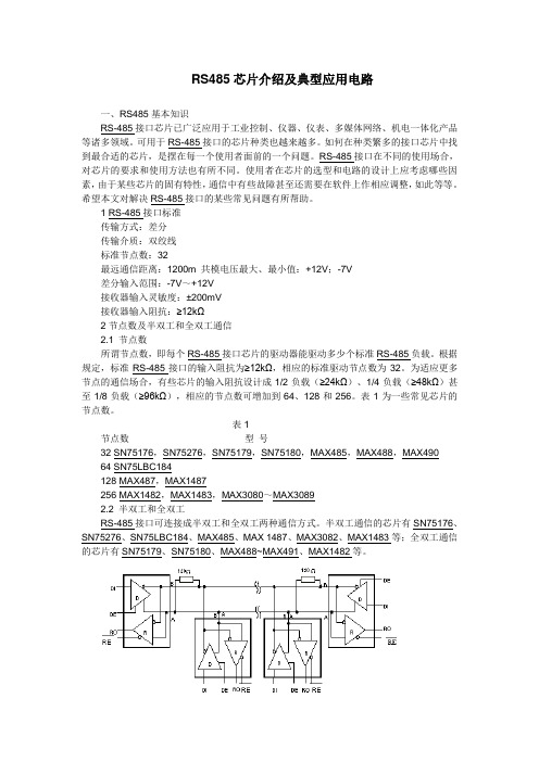
1 RS-485接口标准传输方式:差分传输介质:双绞线标准节点数:32最远通信距离:1200m 共模电压最大、最小值:+12V;-7V差分输入范围:-7V~+12V接收器输入灵敏度:±200mV接收器输入阻抗:≥12kΩ2 节点数及半双工和全双工通信2.1 节点数所谓节点数,即每个RS-485接口芯片的驱动器能驱动多少个标准RS-485负载。
根据规定,标准RS-485接口的输入阻抗为≥12kΩ,相应的标准驱动节点数为32。
为适应更多节点的通信场合,有些芯片的输入阻抗设计成1/2负载(≥24kΩ)、1/4负载(≥48kΩ)甚至1/8负载(≥96kΩ),相应的节点数可增加到64、128和256。
表1为一些常见芯片的节点数。
表1节点数型号32 SN75176,SN75276,SN75179,SN75180,MAX485,MAX488,MAX49064 SN75LBC184128 MAX487,MAX1487256 MAX1482,MAX1483,MAX3080~MAX30892.2 半双工和全双工RS-485接口可连接成半双工和全双工两种通信方式。
半双工通信的芯片有SN75176、SN75276、SN75LBC184、MAX485、MAX 1487、MAX3082、MAX1483等;全双工通信的芯片有SN75179、SN75180、MAX488~MAX491、MAX1482等。
RS485典型电路经典

RS485典型电路经典1 概述RS-485建议性标准作为⼀种多点差分数据传输的电⽓规范,现已成为业界应⽤最为⼴泛的标准通信接⼝之⼀,这种通信接⼝允许在简单的⼀对双绞线上进⾏多点双向通信,它所具有的噪声抑制能⼒、数据传输速率、电缆长度及可靠性是其他标准⽆法⽐拟的,因此许多不同领域都采⽤RS-485作为数据传输链路,它是⼀种极为经济并具有相当⾼的噪声抑制、传输速率、传输距离和宽共模范围的通信平台。
RS-485是⼀种在⼯业上作为数据交换的⼿段⽽⼴泛使⽤的串⾏通信⽅式,数据信号采⽤差分传输⽅式,也称作平衡传输,因此具有较强的抗⼲扰能⼒。
它使⽤⼀对双绞线,将其中⼀线定义为A ,另⼀线定义为B 。
通常情况下, RS-485的信号在传送出去之前会先分解成正负对称的两条线路(即我们常说的A 、B 信号线),当到达接收端后,再将信号相减还原成原来的信号。
发送驱动器A 、B 之间的正电平在+2~+6V ,是⼀个逻辑状态;负电平在-2~-6V ,是另⼀个逻辑状态;另有⼀个信号地C ,在RS-485中还有⼀“使能”端。
“使能”端是⽤于控制发送驱动器与传输线的切断与连接。
当“使能”端起作⽤时,发送驱动器处于⾼阻状态,称作“第三态”,即它是有别于逻辑“1”与“0”的第三态。
接收器也与发送端相对的电平逻辑规定,收、发端通过平衡双绞线将AA 与BB 对应相连,当在接收端AB 之间(DT)=(D+) - (D-)有⼤于+200mV 的电平时,输出正逻辑电平,⼩于-200mV 时,输出负逻辑电平。
接收器接收平衡线上的电平范围通常在200mV ⾄6V 之间。
该应⽤现已经被⼴泛⽤于公司批控仪,R7系列产品的485通讯。
Z LF2 主要性能指标DS75176B 芯⽚技术性能指标:供电电压范围:4.75V to 5.25V ;接收输⼊阻抗:12K ;最⼤接收器数量:32个;共模输⼊电压范围:-7V to 12V ;滞回电压:70mV ;关键芯⽚管脚说明:RE 管脚:接收器输出使能(低电平有效)。
- 1、下载文档前请自行甄别文档内容的完整性,平台不提供额外的编辑、内容补充、找答案等附加服务。
- 2、"仅部分预览"的文档,不可在线预览部分如存在完整性等问题,可反馈申请退款(可完整预览的文档不适用该条件!)。
- 3、如文档侵犯您的权益,请联系客服反馈,我们会尽快为您处理(人工客服工作时间:9:00-18:30)。
号传输时,正端A+的电平大约为3.2V,负端B一的电平大约为
1.6V,即使有千扰信号,却很难产生串行通信的起始信号0,从而
增加了总线抗干扰的能力
在 总 线 末端接一个匹配电阻,吸收总线上的反射信号,保证
正常传输信号干净、无毛刺。匹配电阻的取值应该与总线的特性
阻抗相当。当总线上没有信号传输ห้องสมุดไป่ตู้,总线处于悬浮状态,容易受
干扰信号的影响。将总线上差分信号的正端A十和+5电源间接一
个10K的电阻;正端A十和负端B-间接一个IOK的电阻;负端B-