STMC109 高端电流检测芯片
RK109DT RK109DTX 微波 红外双鉴入侵探测器 安装说明书

RK109DT/RK109DTX 微波/红外双鉴入侵探测器安装说明书1.RK109DTX (微波/被动红外/防下潜型)及RK109DT (微波/被动红外型)是微处理器控制的双技术入侵探测器。
红外与微波技术相结合,互相补充以确保最可靠的探测效果并防止误报。
实际运动识别运算法则的出现,使得RK109DT(X)系列产品优于其它的双鉴探测器。
这种先进的运动分析法使得RK109DT(X)能够将人体的实际运动因素与其它经常导致误报的干扰因素区分开来。
RK109DT(X)的另一独特优点在于其微波运动模拟电路,它可以模拟人体在微波区域移动产生的效果。
这种模拟程序定期运行以供自检,监督并确保微波探测的正常工作。
此外,还运用短时间热脉冲定期对热电传感器及其电路进行检测。
如果它们不能正常工作,会触发出错报警。
为了弥补前透镜的探测范围,RK109DT(X)还在正面机盖的底部安装了一个向下的透镜。
此透镜用于防止从探测器的下面非法接触探测器。
2. 一般参数输入电压:9-16 VDC 工作电流:12 VDC 时大约为26 mA 屏蔽继电器(RK109DT(X)):约60 秒红外部分 透镜数据:34光束,900视角最大覆盖面积:9 x 9 m (30 x 30 ft)垂直调整:+2至-12,具有垂直调整标尺 传感器:双源低噪音热电传感器触发指示:绿色LED 灯闪烁长达5秒 灵敏度调节:可选择,1或2个动作微波部分发 射 器:DRO-稳定型微波传送带 频 率:2.45 GHz探测范围:可在25%至100%(3 m - 9 m )之间调整 触发指示:绿色LED 灯亮,时间长达5秒 报警器,防拆及出错数据报警指示:如果2种探测都被触发,红色LED 灯亮2-3秒 继电器触点:常闭,额定值:0.1 A/30 VDC ;18Ω电阻与触点串联报警持续时间:2-3 秒(红色LED 灯亮且输出继电器触点断开)防拆开关触点:常闭,50 mA/30 VDC 出错输出:常开集电极,最大100 mA 出错/屏蔽指示:红绿灯交替闪烁,且出错输出被拉向低档位物理性能尺寸: 104 x 60 x 35 mm 重量: 86 g安装直接安装:装于平面或墙角(无需支架),最高2.4 m环境条件工作温度:-100C 至500C 贮存温度:-200C 至600CRFI 保护:大于30 V/m (20 MHz 至1000 MHz)3. 3.1 总体原则在选择安装位置时必须注意以下几个重要原则:微波辐射可以穿透玻璃和非金属的墙壁。
高精度电压电流检测模块产品说明书

高精度电压电流检测模块产品说明书CAN PMU连接示意图软件设置ArduPilot 固件(飞行控制器的固件)PX4固件(飞行控制器的固件)在Mission planner 的全部参数表设置以下参数并在写入后重启:在QGroundControl 参数列表中设置以下参数并在写入后重启:CAN_P1_DRIVER=1CAN_P2_DRIVER=1BATT_MONITOR=8(如果使用监视器1)Uavcan_enble 设置为sensors Automatic config(自动配置)注意:请使用AC3.6/AP3.9(含)以上版本的固件注意:PX4固件在1.10或更高版本中支持UAVCAN电源检测模块规格参数基本参数处理器输入电压最大电流电压准确度*电流准确度分辨率STM32F412 100Mhz 512K Flash 256K RAM 6-62V(2-15S)110A±0.05V±0.1A0.01A/V6000W/90S 5000W 5.4V/5A UAVCAN -20℃ ~ +100℃支持工厂校准,用户无需校准最大输出功率最大稳定输出功率稳压输出(Power)通信协议工作温度固件升级校准设置IN/OUTPowerXT90(线材端)/Amass 8.0(模块端)5025850670接口类型尺寸重量CAN PMU 电调连接线X7系列飞控电源线v5系列飞控电源线Pixhawk 飞控连接线X1X1X1X1产品外观46.5mm×38.5mm×22.5mm 76g 配件清单- 请仔细阅读产品的使用说明书- 连接电池前,请仔细检查连线- 请在额定的电压、电流、功率下使用- 请阅读文档中心进行配置和使用- 严禁自行拆装固件升级教程请访问CUAV 文档中心: 注意事项固件升级关于产品的更多信息,请访问CUAV 官方文档中心: 及官方网站:更多资料Thank you for choosing CAN PMU ! CAN PMU interface definition Please read this guide before using!Battery + Battery -ESC + ESC -Status lightCAN PMU connection schematic diagram 5V +5V +C A N _H C A N _L G N D G N D 5T R D I C GCAN PMU connection schematic diagramSoftware settingsArduPilot firmware (flight controller firmware)Set the following parameters in the Mission planner's full parameter list and restart after writing:CAN_P1_DRIVER=1CAN_P2_DRIVER=1BATT_MONITOR=8 (If using monitor 1)Note: Please use the firmware of AC3.6/AP3.9 (included) or higher.PX4 firmware (flight controller firmware)Set the following parameters in the QGroundControl parameter list and restart after writing:Uavcan_enble set to sensors Automatic configNote: PX4 firmware supports UAVCAN power detection module in 1.10 or higher.Specifications Basic parametersProcessor Voltage input Max current Voltage accuracy Current accuracy Resolution STM32F412 100Mhz 512K Flash 256K RAM 6-62V(2-15S)110A±0.05V±0.1A0.01A/V6000W/90S 5000W 5.4V/5A UAVCAN -20℃ ~ +100℃Support No need Max output powerMax stable powerPower port outputprotocolOperating tempFirmware upgradeCalibrationIN/OUTPowerXT90(Cable end)/Amass 8.0(Module end)5025850670Interface TypeSizeWeightCAN PMUX7 series power cableV5 Series Power Cable X1X1X1Appearance46.5mm×38.5mm×22.5mm 76g Packing ListNotes- Please read the product manual carefully.- Please check the connection carefully before connecting the battery- Please use at rated voltage, current and power- Please read the documentation center for configuration and use- Do not disassembleFirmware upgradePlease visit the CUAV Documentation Center for a firmware upgrade tutorial: More infoFor more information on the product, please visit the CUAV Official Documentation Center:And official website:。
LC10A 超低功耗,I2C 接口 高精度心率检测传感器 使用说明书
焊接注意事项:由于 LC10A 为透明封装,高温状态持续请勿超过 10S,以免损坏外 观或直接导致芯片失效;
成都维客昕微电子有限公司
[3]
7 结构设计推荐
LC10A 说明书
为了更好地发挥出芯片性能,我们推荐了芯片硬件结构方案,包括 LED 的布局、玻璃丝 印尺寸、挡板尺寸以及 IC 与玻璃间隙,具体结构如下所示。
发生壳料内部窜光。 *注:以上结构、硬件、光路若不使用推荐方案,维客不保证性能;不支持使用双色模和 IML 工艺。
成都维客昕微电子有限公司
[6]
LC10A 说明书
8 LED 性能参数及辅料说明
LC10A 心率芯片对 Green、IR 的光效及压降要求如下表所示,可根据下表 LED 参数 自行选择 LED 供应商;
VDDIO 2
3
4
5
PD
LC10A
10
9
8
C1 C2
7 VCP 10u 10u
6 VDD C3100n
INT SCL SDA VDD VDDIO
主板
图 2 LC10A 推荐应用电路
推荐应用电路设计注意事项: a、建议心率模块使用单独 LDO 供电; b、如 MCU 通信、中断、复位 IO 采用 1.8V 电压,则 VDDIO 需要单独接 1.8V 电源;如
恒流源芯片9910
控制电压为低电平时,MOSFET关断,储能电感通过整流肖特基二极管释放能量,从而点这LED灯串。
由于高压供电,MOSFET应选用耐高压产品,RCS为电流检测电阻,MOSFET的电流流过RCS时,全产生一个电压降UCS,当VSC达到约250mV 阀值电压时,MOSFET关断,从而控制MOSFET管的开通/关断,使储能电感周期性的充电放电,完成对LED的恒流驱动,LED灯驱动的占空比为D=Vout/Vin。
通过储能电感的最大电流为I LM A X=250/R C S(mA),通过LED的平均电流ILED约为3R×I L M AX。
RCS阻值不同,就可设置通过LED的驱动电流,R C S越小,输出电流越大。
R C S的选择公式如下:Rcs=250mV(I LED+0.5×I L)IL E D 为通过LED灯的电流;IL为通过电感L的峰值电流例如:IL =150mA IL E D=500mA 则RC S=0.43Ω(1)电感的选择电感的电感量的选用原则是确保流过电感的电流变化值,远小于通过电感的最大电流值。
在正常工作中,电感处于一个充电放电的状态,当输入电压和输出电压的压差较大时,应相应加大电感的值,当压差小时可以用较小的电感。
一般取值在几百微享到十几毫享,视实际应用而定。
(2)MOS 管的选择在220V交流供电情况下,首先要考虑MOSFET的耐压,一般要求MOSFET的耐压高于600V。
其次,根据驱动LED灯电流的大小,选择MOSFET的ID S最大电流。
一般情况下,应选用MOSFET的ID S最大电流是LED灯驱动电流的5倍以上。
另外MOSFET的内阻要小;RD S 应小于0.5欧以下,RD S越小,在MOS管上面的功率损耗越小,电路的变换效率就越高。
在12V/24V直流供电情况下,首先考虑的是ID S 最大电流值和RD S值,RD S越小越好,选择小于0.2欧以下的MOSFET管。
CSL109A
CSL109A数字式线路保护装置技术说明书( V 1.00 版)2000年10月1 概述 (1)2 主要技术数据 (1)3 结构 (4)4 硬件说明 (4)4.1 交流插件 (4)4.2 模数变换插件 (5)4.3 故障录波插件 (5)4.4 CPU插件 (6)4.5 继电器插件 (7)4.6 电源插件 (8)4.7 人机对话板 (8)4.8 选供的打印机接口和工程师站 (9)4.9 装置端子说明 (10)5 人机对话 (10)5.1 正常运行显示 (10)5.2 各种功能键 (12)6装置功能说明 (15)6.1启动元件 (15)6.2距离保护 (15)6.3和流保护 (17)6.4过流保护 (17)6.5手合加速回路 (17)6.6 PT断线 (17)6.7 CT断线 (17)6.8 故障处理软件流程 (17)6.9 与变电站综合自动化系统配合 (22)6.10 故障录波插件功能 (23)7 定值管理 (24)7.1 概述 (24)7.2 定值清单 (24)7.3 故障录波插件定值 (26)8 用户安装调试说明 (29)8.1 通电前检查 (29)8.2 装置通电检查 (30)8.2.1 直流稳压电源通电检查 (30)8.2.2 整机通电检查 (30)8.2.3 开入量检查 (30)8.2.4 零漂检查 (30)8.2.5 电流电压刻度检查 (30)8.2.6 定值输入 (31)8.2.7 开出传动试验 (31)8.3 模拟短路试验 (31)8.3.1 试验目的及项目 (31)8.3.2 试验注意事项 (31)8.4 耐压试验 (31)9 维护运行 (31)9.1 装置的投运 (31)9.2 装置的运行 (31)9.3 保护的动作信号及报告 (32)9.4 报告信息 (32)9.4.1正常显示信息 (32)9.4.2CSL109A保护动作及告警信息 (32)9.5 其它注意事项 (33)10 维修指南 (34)11 贮存 (34)* 订货须知 (34)** 附图 (35)附图1 面板布置图 (36)附图2 CSL109A装置插件位置图 (37)附图3 各插件联系简图 (38)附图4 交流插件原理图 (39)附图5 VFC芯片电压频率特性 (40)附图6 模数变换插件原理图 (41)附图7 继电器插件原理图 (42)附图8 电源插件原理图 (43)附图9 CSL109A背板端子图(非综自) (44)附图10CSL109A背板端子图(综自硬压板) (45)附图11 CSL109A背板端子图(综自软压板) (46)附图12CSL109A背板连线图 (47)附图13CPU插件原理图 (48)附图14 -1MMI插件原理图 (49)附图14-2 MMI插件原理图 (50)附图15-1 录波插件原理图 (51)附图15-2 录波插件原理图 (52)1.概述本装置系由微型计算机构成的以相间距离保护和和流保护为核心的成套线路保护装置,主要适用于220KV两相供电的电铁线路。
TB67S109AFNAG(CPEL 大功率驱动芯片之王

TOSHIBA BiCD Integrated Circuit Silicon MonolithicTB67S109AFNAG CLOCK-in controlled Bipolar Stepping Motor Driver・・・・・・・・・・・・Pin assignment (TB67S109AFNAG)Please mount the exposed pad of the HSSOP package to heatsink .TB67S109A Block diagramFunctional blocks/circuits/constants in the block chart etc. may be omitted or simplified for explanatory purposes.Application NotesAll the grounding wires of the TB67S109A must run on the solder mask on the PCB and be externally terminated at only one point. Also, a grounding method should be considered for efficient heat dissipation.Careful attention should be paid to the layout of the output, VDD(VM) and GND traces, to avoid short circuits across output pins or to the power supply or ground. If such a short circuit occurs, the device may be permanently damaged.Also, the utmost care should be taken for pattern designing and implementation of the device since it has power supply pins (VM, RS, OUT, GND) through which a particularly large current may run. If these pins are wired incorrectly, an operation error may occur or the device may be destroyed.The logic input pins must also be wired correctly. Otherwise, the device may be damaged owing to a current running through the IC that is larger than the specified current.Pin explanations TB67S109AFNAGINPUT/OUTPUT equivalent circuit (TB67S109A)The equivalent circuit diagrams may be simplified or some parts of them may be omitted for explanatory purposes.Function explanation (Stepping motor)CLK FunctionEach up-edge of the CLK signal will shift the motor’s electrical angle per step.ENABLE functionis recommended.Step resolution setting and initial angle [Full step resolution][Half step resolution (Type B)]MO output shown in the timing chart is when the MO pin is pulled up. Timing charts may be simplified for explanatory purpose.MO output shown in the timing chart is when the MO pin is pulled up. Timing charts may be simplified for explanatory purpose. CWCCWStep setting and current percentageLO(Error detect signal) output functionWhen Thermal shutdown(TSD) or Over-current shutdown(ISD) is applied, the LO voltage will be switched to Low(GND) level.Decay functionADMD(Advanced Dynamic Mixed Decay) constant current controlThe Advanced Dynamic Mixed Decay threshold, which determines the current ripple level during current feedback control, is a unique value.fchopADMDth (Advanced Dynamic Mixed Decay threshold) Timing charts may be simplified for explanatory purpose.ADMD current waveform・When the next current step is higher :・mode.・When the next current step is lower :・OSCOutput transistor function modeVM VM VMCalculation of the Predefined Output CurrentFor PWM constant-current control, this IC uses a clock generated by the OSCM oscillator.The peak output current (Setting current value) can be set via the current-sensing resistor (RS) and the referencevoltage (Vref), as follows:Iout(max) = Vref(gain) ×Vref(gain) : the Vref decay rate is 1/ 5.0 (typ.)For example : In the case of a 100% setupwhen Vref = 3.0 V, Torque=100%,RS=0.51Ω, the motor constant current (Setting current value) will becalculated as:I out = 3.0V / 5.0 / 0.51Ω= 1.18 ACalculation of the OSCM oscillation frequency (chopper reference frequency)An approximation of the OSCM oscillation frequency (fOSCM) and chopper frequency (fchop)can be calculated by the following expressions.fOSCM=1/[0.56x{Cx(R1+500)}]………C,R1: External components for OSCM (C=270pF , R1=5.1kΩ => About fOSCM= 1.12MHz(Typ.)) fchop = fOSCM / 16………fOSCM=1.12MHz => fchop =About 70kHzIf chopping frequency is raised, Rippl of current will become small and wave-like reproducibility will improve.However, the gate loss inside IC goes up and generation of heat becomes large.By lowering chopping frequency, reduction in generation of heat is expectable.However, Rippl of current may become large.It is a standard about about 70 kHz. A setup in the range of 50 to 100 kHz is recommended.byanyis (exciting mode, operating time, and so on), ambient temperature, and heat conditions (board condition and so on).isavoidAC Electrical Specification (Ta = 25°C, VM = 24 V, 6.8 mH/5.7 Ω)Timing charts may be simplified for explanatory purpose.Package DimensionsWeight TBDg (typ.) P-HSSOP36-1116-0.65-001 (unit :mm)Notes on ContentsBlock DiagramsSome of the functional blocks, circuits, or constants in the block diagram may be omitted or simplified for explanatory purposes.Equivalent CircuitsThe equivalent circuit diagrams may be simplified or some parts of them may be omitted for explanatory purposes.Timing ChartsTiming charts may be simplified for explanatory purposes.Application CircuitsThe application circuits shown in this document are provided for reference purposes only. Thorough evaluation is required, especially at the mass-production design stage.Toshiba does not grant any license to any industrial property rights by providing these examples of application circuits.Test CircuitsComponents in the test circuits are used only to obtain and confirm the device characteristics. These components and circuits are not guaranteed to prevent malfunction or failure from occurring in the application equipment.IC Usage ConsiderationsNotes on handling of ICs(1) The absolute maximum ratings of a semiconductor device are a set of ratings that must not be exceeded,even for a moment. Do not exceed any of these ratings.Exceeding the rating(s) may cause devicebreakdown, damage or deterioration, and may result in injury by explosion or combustion.(2)Use an appropriate power supply fuse to ensure that a large current does not continuously flow in thecase of overcurrent and/or IC failure. The IC will fully break down when used under conditions thatexceed its absolute maximum ratings, when the wiring is routed improperly or when an abnormalpulse noise occurs from the wiring or load, causing a large current to continuously flow and thebreakdown can lead to smoke or ignition. To minimize the effects of the flow of a large current in thecase of breakdown, appropriate settings, such as fuse capacity, fusing time and insertion circuitlocation, are required.(3) If your design includes an inductive load such as a motor coil, incorporate a protection circuit into thedesign to prevent device malfunction or breakdown caused by the current resulting from the inrushcurrent at power ON or the negative current resulting from the back electromotive force at power OFF.IC breakdown may cause injury, smoke or ignition. Use a stable power supply with ICs with built-inprotection functions. If the power supply is unstable, the protection function may not operate, causingIC breakdown. IC breakdown may cause injury, smoke or ignition.(4) Do not insert devices in the wrong orientation or incorrectly. Make sure that the positive and negativeterminals of power supplies are connected properly.Otherwise, the current or power consumption may exceed the absolute maximum rating, andexceeding the rating(s) may cause device breakdown, damage or deterioration, and may result ininjury by explosion or combustion.In addition, do not use any device inserted in the wrong orientation or incorrectly to which current isapplied even just once.(5)Carefully select external components (such as inputs and negative feedback capacitors) and loadcomponents (such as speakers), for example, power amp and regulator.If there is a large amount of leakage current such as from input or negative feedback capacitor, the ICoutput DC voltage will increase. If this output voltage is connected to a speaker with low inputwithstand voltage, overcurrent or IC failure may cause smoke or ignition. (The overcurrent may causesmoke or ignition from the IC itself.) In particular, please pay attention when using a Bridge Tied Load(BTL) connection-type IC that inputs output DC voltage to a speaker directly.Points to remember on handling of ICsOvercurrent detection CircuitOvercurrent detection circuits (referred to as current limiter circuits) do not necessarily protect ICs under all circumstances. If the overcurrent detection circuits operate against the overcurrent, clear the overcurrent status immediately.Depending on the method of use and usage conditions, exceeding absolute maximum ratings may cause the overcurrent detection circuit to operate improperly or IC breakdown may occur before operation. In addition, depending on the method of use and usage conditions, if overcurrent continues to flow for a long time after operation, the IC may generate heat resulting in breakdown.Thermal Shutdown CircuitThermal shutdown circuits do not necessarily protect ICs under all circumstances. If the thermal shutdown circuits operate against the over-temperature, clear the heat generation status immediately.Depending on the method of use and usage conditions, exceeding absolute maximum ratings may cause the thermal shutdown circuit to operate improperly or IC breakdown to occur before operation.Heat Radiation DesignWhen using an IC with large current flow such as power amp, regulator or driver, design the device so that heat is appropriately radiated, in order not to exceed the specified junction temperature (TJ) at any time or under any condition. These ICs generate heat even during normal use. An inadequate IC heat radiation design can lead to decrease in IC life, deterioration of IC characteristics or IC breakdown. In addition, when designing the device, take into consideration the effect of IC heat radiation with peripheral components.Back-EMFWhen a motor rotates in the reverse direction, stops or slows abruptly, current flows back to the motor’s power supply owing to the effect of back-EMF. If the current sink capability of the power supply is small, the device’s motor power supply and output pins might be exposed to conditions beyond the absolute maximum ratings. To avoid this problem, take the effect of back-EMF into consideration in system design.RESTRICTIONS ON PRODUCT USE∙Toshiba Corporation, and its subsidiaries and affiliates (collectively "TOSHIBA"), reserve the right to make changes to the information in this document, and related hardware, software and systems (collectively "Product") without notice.∙This document and any information herein may not be reproduced without prior written permission from TOSHIBA. Even with TOSHIBA's written permission, reproduction is permissible only if reproduction is without alteration/omission.∙Though TOSHIBA works continually to improve Product's quality and reliability, Product can malfunction or fail. Customers are responsible for complying with safety standards and for providing adequate designs and safeguards for their hardware, software and systems which minimize risk and avoid situations in which a malfunction or failure of Product could cause loss of human life, bodily injury or damage to property, including data loss or corruption. Before customers use the Product, create designs including the Product, or incorporate the Product into their own applications, customers must also refer to and comply with (a) the latest versions of all relevant TOSHIBA information, including without limitation, this document, the specifications, the data sheets and application notes for Product and the precautions and conditions set forth in the "TOSHIBA Semiconductor Reliability Handbook" and (b) the instructions for the application with which the Product will be used with or for. Customers are solely responsible for all aspects of their own product design or applications, including but not limited to (a) determining the appropriateness of the use of this Product in such design or applications; (b) evaluating and determining the applicability of any information contained in this document, or in charts, diagrams, programs, algorithms, sample application circuits, or any other referenced documents; and (c) validating all operating parameters for such designs and applications. TOSHIBA ASSUMES NO LIABILITY FOR CUSTOMERS' PRODUCT DESIGN OR APPLICATIONS.∙PRODUCT IS NEITHER INTENDED NOR WARRANTED FOR USE IN EQUIPMENTS OR SYSTEMS THAT REQUIRE EXTRAORDINARILY HIGH LEVELS OF QUALITY AND/OR RELIABILITY, AND/OR A MALFUNCTION OR FAILURE OF WHICH MA Y CAUSE LOSS OF HUMAN LIFE, BODILY INJURY, SERIOUS PROPERTY DAMAGE AND/OR SERIOUS PUBLIC IMPACT ("UNINTENDED USE"). Except for specific applications as expressly stated in this document, Unintended Use includes, without limitation, equipment used in nuclear facilities, equipment used in the aerospace industry, medical equipment, equipment used for automobiles, trains, ships and other transportation, traffic signaling equipment, equipment used to control combustions or explosions, safety devices, elevators and escalators, devices related to electric power, and equipment used in finance-related fields. IF YOU USE PRODUCT FOR UNINTENDED USE, TOSHIBA ASSUMES NO LIABILITY FOR PRODUCT. For details, please contact your TOSHIBA sales representative.∙Do not disassemble, analyze, reverse-engineer, alter, modify, translate or copy Product, whether in whole or in part.∙Product shall not be used for or incorporated into any products or systems whose manufacture, use, or sale is prohibited under any applicable laws or regulations.∙The information contained herein is presented only as guidance for Product use. No responsibility is assumed by TOSHIBA for any infringement of patents or any other intellectual property rights of third parties that may result from the use of Product. No license to any intellectual property right is granted by this document, whether express or implied, by estoppel or otherwise.∙ABSENT A WRITTEN SIGNED AGREEMENT, EXCEPT AS PROVIDED IN THE RELEVANT TERMS AND CONDITIONS OF SALE FOR PRODUCT, AND TO THE MAXIMUM EXTENT ALLOWABLE BY LAW, TOSHIBA (1) ASSUMES NO LIABILITYWHATSOEVER, INCLUDING WITHOUT LIMITATION, INDIRECT, CONSEQUENTIAL, SPECIAL, OR INCIDENTAL DAMAGES OR LOSS, INCLUDING WITHOUT LIMITATION, LOSS OF PROFITS, LOSS OF OPPORTUNITIES, BUSINESS INTERRUPTION AND LOSS OF DATA, AND (2) DISCLAIMS ANY AND ALL EXPRESS OR IMPLIED WARRANTIES AND CONDITIONS RELATED TO SALE, USE OF PRODUCT, OR INFORMATION, INCLUDING WARRANTIES OR CONDITIONS OF MERCHANTABILITY, FITNESS FOR A PARTICULAR PURPOSE, ACCURACY OF INFORMATION, OR NONINFRINGEMENT.∙Do not use or otherwise make available Product or related software or technology for any military purposes, including without limitation, for the design, development, use, stockpiling or manufacturing of nuclear, chemical, or biological weapons or missile technology products (mass destruction weapons). Product and related software and technology may be controlled under the applicable export laws and regulations including, without limitation, the Japanese Foreign Exchange and Foreign Trade Law and the U.S. Export Administration Regulations. Export and re-export of Product or related software or technology are strictly prohibited except in compliance with all applicable export laws and regulations.∙Please contact your TOSHIBA sales representative for details as to environmental matters such as the RoHS compatibility of Product.Please use Product in compliance with all applicable laws and regulations that regulate the inclusion or use of controlled substances, including without limitation, the EU RoHS Directive. TOSHIBA ASSUMES NO LIABILITY FOR DAMAGES OR LOSSESOCCURRING AS A RESULT OF NONCOMPLIANCE WITH APPLICABLE LAWS AND REGULATIONS.。
新型电压检测芯片PT8A610x及其应用
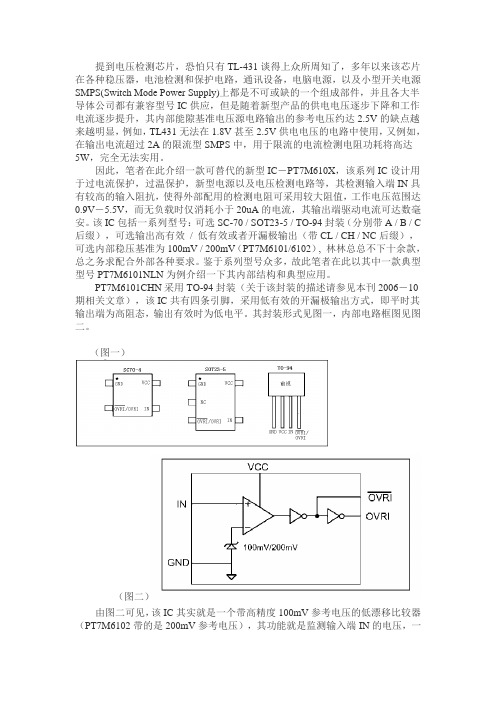
提到电压检测芯片,恐怕只有TL-431谈得上众所周知了,多年以来该芯片在各种稳压器,电池检测和保护电路,通讯设备,电脑电源,以及小型开关电源SMPS(Switch Mode Power Supply)上都是不可或缺的一个组成部件,并且各大半导体公司都有兼容型号IC供应,但是随着新型产品的供电电压逐步下降和工作电流逐步提升,其内部能隙基准电压源电路输出的参考电压约达2.5V的缺点越来越明显,例如,TL431无法在1.8V甚至2.5V供电电压的电路中使用,又例如,在输出电流超过2A的限流型SMPS中,用于限流的电流检测电阻功耗将高达5W,完全无法实用。
因此,笔者在此介绍一款可替代的新型IC-PT7M610X,该系列IC设计用于过电流保护,过温保护,新型电源以及电压检测电路等,其检测输入端IN具有较高的输入阻抗,使得外部配用的检测电阻可采用较大阻值,工作电压范围达0.9V-5.5V,而无负载时仅消耗小于20uA的电流,其输出端驱动电流可达数毫安。
该IC包括一系列型号:可选SC-70 / SOT23-5 / TO-94封装(分别带A / B / C 后缀),可选输出高有效/ 低有效或者开漏极输出(带CL / CH / NC后缀),可选内部稳压基准为100mV / 200mV(PT7M6101/6102), 林林总总不下十余款,总之务求配合外部各种要求。
鉴于系列型号众多,故此笔者在此以其中一款典型型号PT7M6101NLN为例介绍一下其内部结构和典型应用。
PT7M6101CHN采用TO-94封装(关于该封装的描述请参见本刊2006-10期相关文章),该IC共有四条引脚,采用低有效的开漏极输出方式,即平时其输出端为高阻态,输出有效时为低电平。
其封装形式见图一,内部电路框图见图二。
(图一)(图二)由图二可见,该IC其实就是一个带高精度100mV参考电压的低漂移比较器(PT7M6102带的是200mV参考电压),其功能就是监测输入端IN的电压,一旦达到或超过参考电压,输出端立即翻转。
高端电流检测芯片

高端电流检测芯片高端电流检测芯片电流检测芯片是一种用于监测和测量电流的电子元件,广泛应用于各种电子设备和系统中。
随着电子技术的不断发展,人们对电流检测芯片的要求也越来越高。
高端电流检测芯片是指具有更高性能和更多功能的电流检测芯片,下面将介绍一种高端电流检测芯片的特点和应用。
高端电流检测芯片具有以下特点:1. 高精度:高端电流检测芯片的核心功能是精确测量电流,因此高精度是其最重要的特点之一。
一般情况下,高端电流检测芯片的测量精度可以达到几个百分点以下,能够满足各种精密测量的需求。
2. 宽测量范围:高端电流检测芯片具有较宽的测量范围,可以适用于不同电流大小的应用场景。
同时,高端电流检测芯片还可以根据需要进行范围调节,使其更加灵活多变。
3. 快速响应:高端电流检测芯片能够实时响应电流变化,并能够快速采集和处理电流信号。
这样可以提高系统的响应速度和实时性,保证系统的稳定性和可靠性。
4. 低功耗:高端电流检测芯片采用先进的低功耗技术,能够在高性能的同时保证较低的功耗。
这对于需要长时间运行的电子设备和系统来说非常重要,可以提高能源利用效率和延长电池寿命。
5. 多功能:高端电流检测芯片可以集成多种功能和特性,如电流保护、短路保护、过流保护等,可以实现更为完善的电流监测和保护功能。
同时,高端电流检测芯片还可以与其他芯片和模块进行集成,实现更多应用场景的需求。
高端电流检测芯片在各种电子设备和系统中有广泛的应用,主要包括以下几个方面:1. 电动汽车:高端电流检测芯片可以用于电动汽车充电桩和电池管理系统中,实时监测并控制电流的输入和输出,保证电池的正常运行和延长电池寿命。
2. 工业自动化:在工业自动化系统中,高端电流检测芯片可以用于电机驱动和控制模块中,监测电机的工作状态和电流的变化,保证电机的稳定运行和故障检测。
3. 可穿戴设备:高端电流检测芯片可以用于可穿戴设备中的电池管理和电流监测,可以实时检测设备的电流消耗和充电状态,为用户提供更加便捷和可靠的使用体验。
大学生电子设计竞赛中电流检测方案的设计
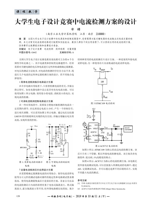
—科教导刊(电子版)·2019年第33期/11月(下)—120大学生电子设计竞赛中电流检测方案的设计牟峰(南京工业大学计算机学院江苏·南京210000)摘要全国大学生电子设计竞赛中的电源类和控制类题型中,经常需要对某关键电路的电流做出定性或定量的检测。
本文对常见电流检测电路进行梳理和实验验证。
提供几种在不同应用场景下,可以很好应用的电流检测方案。
供参赛学生做赛前训练和竞赛技术准备。
关键词电子设计竞赛电流检测简单检测定量测量中图分类号:G642文献标识码:A 全国大学生电子设计竞赛是教育部高教司主办的6个全国性学科竞赛之一。
其中电源类和控制类竞赛题型中,经常需要对关键电路的电压和电流进行定性控制或精确定量测量。
对电压的测试方法较多,对电流的检测同学往往方法不多。
现进行几个电流的定性和定量检测方案的设计,供不同场合选择使用。
1简单电流检测指示电路设计方案在许多电路应用场景下,只需要检测电流的有无,并做出指示即可。
如充电器电路中显示是否有充电电流功能。
可以使用如图1所示电路,使用很小的电阻,消耗很小的电压,实现电流的检测。
2可调电流检测控制电路设计方案在一些应用场景中,需要很方便地对被检测的电流在一定范围内调节,在达到设定电流大小时,产生一个控制信号,进行相关调整。
可以采用如图2所示电路,通过电压比较器LM339的同相端和反向端的电压比较,在输出端输出电压的高低,实现所需的控制。
图1:简单电流检测指示图2:可调电流检测控制电路电路3定量电流检测芯片应用设计方案在需要精确定量测量电流的应用场合,使用电流采样电阻等分立元件的测试电路对器件的稳定性和电路调试要求都很高。
使用电流测量集成芯片是很好的方案。
各家公司出品的电流检测芯片内部的原理有基于电容式隔离放大、塔式隔离放大、霍尔隔离放大等不同,但外围电路都比较类似。
现介绍两种常用的电流检测芯片设计方案。
一种是使用外接电流采样电阻,另一种使用芯片内部集成的电流采样电阻。
电流检测芯片资料

电源电压
模拟输 入,V+IN,V-IN (2)
差分电压 ef2,输出
到任一引脚的输入电流
存储温度
结温
人体模型 (HBM)
额定 ESD:
充电器件模型 (CDM)
机器模型 (MM)
INA282,INA283, INA284,INA285,INA286
+18 -5 至 +5 -14 至 +80 GND-0.3 至 (V+)+0.3
引脚说明
说明 连接到分流电阻器的负输入一侧。 接地 基准电压连接-连接选项请见应用部分。 这个引脚不是内部连接。 NC 引脚应该保持悬空或者连接到 GND。 输出电压 电源 基准电压连接-连接选项请见应用部分。 连接到分流电阻器的正输入一侧。
Copyright © 2009–2012, Texas Instruments Incorporated
这些装置包含有限的内置 ESD 保护。
存储或装卸时,应将导线一起截短或将装置放置于导电泡棉中,以防止 MOS 门极遭受静电损伤。
产品 INA282 INA283 INA284 INA285 INA286
封装/订购信息 (1)
增益 50V/V 200V/V 500V/V 1000V/V 100V/V
封装 SOIC-8 SOIC-8 SOIC-8 SOIC-8 SOIC-8
50 200 500 1000 100
±0.4 ±0.4 0.0008
±0.01 1.5 1
±1.4 ±1.6 0.005
V/V V/V V/V V/V V/V
% % %/°C
% Ω nF
(1) RTI=以输入为基准。 (2) 请见典型特征图Figure 20。 (3) 引脚 REF1 和 REF2 上的电压平均值必须介于 VGND和 (VGND+9V) 的较小值以及 V+ 之间。 (4) 基准分频器精度指定了使用Figure 37中配置的基准分频电阻器间的匹配。 (5) 请见典型特征图Figure 25。
thc63lvd103c原理

thc63lvd103c原理一、概述THC63LVD103C是一种高性能的电流检测芯片,广泛应用于电源、电子设备、马达控制等领域。
该芯片通过检测电流信号,可以实现对电路中电流的精确测量和控制,从而提高系统的稳定性和效率。
二、工作原理1. 电流检测:THC63LVD103C通过精密电阻采样电流信号,将其转换为电压信号,然后通过芯片内部的放大器和滤波器进行处理。
2. 信号处理:芯片内部集成有高性能的放大器和滤波器,可以对采样到的电流信号进行放大和滤波,消除干扰信号的影响,提高测量精度。
3. 输出信号:处理后的电流信号通过芯片的数字输出接口,以数字信号的形式输出,方便与微处理器或控制器进行通信和控制。
三、应用电路1. 电源电路:在电源电路中,THC63LVD103C可以用于检测输出电流,从而实现对输出电压的稳定控制。
2. 电子设备:在电子设备中,THC63LVD103C可以用于马达驱动、电源管理等电路中,实现对电路中电流的精确控制和保护。
3. 马达控制:在马达控制中,THC63LVD103C可以用于检测马达的电流信号,从而实现对马达转速和转向的控制。
四、注意事项1. 采样电阻的选择:根据实际应用场合的需求,选择合适的精密采样电阻,以确保采样信号的准确性和稳定性。
2. 电源干扰:在应用电路中,应采取适当的屏蔽和滤波措施,以防止电源干扰对芯片的影响。
3. 温度特性:THC63LVD103C具有较好的温度特性,但在高温环境下使用时,应采取适当的散热措施,以保证芯片的正常工作。
五、总结THC63LVD103C是一种高性能的电流检测芯片,通过精确检测电流信号,实现对电路中电流的精确控制和保护。
该芯片广泛应用于电源、电子设备、马达控制等领域,具有较高的实用价值。
在实际应用中,应选择合适的采样电阻,采取适当的屏蔽和滤波措施,以保证芯片的正常工作。
N109x 高精度光波形和电波形分析解决方案
是德科技N1090A、N1092A/B/C/D/E 和 N1094A/B DCA-M 光电信号采样示波器技术资料高精度、低成本的光波形和电波形分析解决方案–支持 1 Gb/s 至 28 Gb/s 数据速率–非常低的噪声和抖动–快速采样率,可实现高吞吐量专为制造业而设计的测试解决方案,精度堪比86100 DCA Keysight 86100 数字通信分析仪(DCA)是业界公认的,用以验证光收发信机是否符合通信标准的标准仪器,并且多年以来广受工程师们的青睐。
工程师可以轻松地用它精确测量数字通信波形。
Keysight N109X DCA-M 系列成功传承了 86100 的精华,其中许多高性能元件来自于 86100 示波器主机采集系统,并且借鉴于 861XX 插入式模块中的光通道和电通道硬件。
N1090A 支持1 Gb/s 至 10 Gb/s 测量,而 N1092 和 N1094 适用于 20 至 28 Gb/s 测量(N1092 配以选件 PLK 和 IRC,其数据速率还可进一步得到扩展)。
DCA-M 专为大规模制造测试应用而设计,拥有堪比 86100 示波器的测量精度,并且避免了研发测试解决方案的额外成本。
对于收发信机和元器件的最终用户而言,他们通常都是使用相似精度的高质量测试系统来验证元器件的性能,因此使用 N109X 执行测试,可让您对测试结果高枕无忧。
86100 系列是使用模块来创建波形分析系统,而 N109X 系列的最大区别就在于,它们是外形小巧的、完全集成的仪器。
N109X 系列配有低噪声、高灵敏度,且经过校准的参考接收机(符合行业容差标准),可对 750 nm 到 1630 nm 波长的多模和单模信号进行测试。
N1090A 的噪声可低至 1 μW,而 N1092 的噪声低至 4 μW,确保了此系列的测试系统能够支持极高的动态测量范围。
N1092 的灵敏度显著优于 86100 系统,因此在 PAM-4 波形分析方面是更为出色的解决方案。
【CN109669067A】多通道高精度电流动态实时检测设备【专利】

(19)中华人民共和国国家知识产权局(12)发明专利申请(10)申请公布号 (43)申请公布日 (21)申请号 201910159496.X(22)申请日 2019.03.04(71)申请人 苏州道捷电子科技有限公司地址 215000 江苏省苏州市苏州工业园区苏虹东路188号方正科技园综合办公楼三楼321-13室(72)发明人 吉海军 (74)专利代理机构 苏州谨和知识产权代理事务所(特殊普通合伙) 32295代理人 叶栋(51)Int.Cl.G01R 19/00(2006.01)(54)发明名称多通道高精度电流动态实时检测设备(57)摘要本发明涉及一种多通道高精度电流动态实时检测设备,包括电流采样模块、第一判断模块、电流电压转换模块、第二判断模块、阻断模块、处理模块及计算机模块;电流采样模块获取第一采样电流值,第一判断模块对第一采样电流值进行判断后获得第二采样电流值发送至对等级别的电流电压转换模块,电流电压转换模块将第二采样电流值转换为第一采样电压值后发送至第二判断模块,第二判断模块将第一采样电压值与预存的电压值域范围进行比对后得到第二采样电压值并发送至阻断模块及处理模块,阻断模块接收第二采样电压值后使得部分模块短路,处理模块对第二采样电压值进行处理以获得测试电压值并发送至计算机模块后获得测试电流值,简单且操作方便。
权利要求书1页 说明书5页 附图1页CN 109669067 A 2019.04.23C N 109669067A权 利 要 求 书1/1页CN 109669067 A1.一种多通道高精度电流动态实时检测设备,其特征在于,所述设备包括电流采样模块、第一判断模块、若干个电流电压转换模块、第二判断模块、若干个阻断模块、处理模块、及计算机模块;其中,所述电流采样模块对工作电流进行采样获取第一采样电流值,并将所述第一采样电流值发送至所述第一判断模块,所述第一判断模块接收所述第一采样电流值并将所述第一采样电流值与预存的不同级别的电流值域范围进行比对后获得第二采样电流值,将所述第二采样电流值发送至相对应级别的电流电压转换模块,所述电流电压转换模块接收所述第二采样电流值并将所述第二采样电流值转换为第一采样电压值后发送至所述第二判断模块,所述第二判断模块接收所述第一采样电压值并将所述第一采样电压值与预存的不同级别的电压值域范围进行比对以确定所述第一采样电压值的级别后得到第二采样电压值,将所述第二采样电压值发送至满足级别的阻断模块及处理模块,所述阻断模块接收所述第二采样电压值后使得部分模块短路,所述处理模块接收所述第二采样电压值并对所述第二采样电压值进行线性处理以获得测试电压值,将所述测试电压值发送至所述计算机模块,所述计算机模块接收所述测试电压值并根据换算公式将所述测试电压值转换为测试电流值。
基于ATT7053BU的便携式剩余电流检测电路设计

基于ATT7053BU的便携式剩余电流检测电路设计便携式剩余电流检测电路设计基于ATT7053BU芯片。
ATT7053BU是一款集成的电子断路器,具有非常低的功耗和高精度的测量能力。
它适用于便携式剩余电流检测设备,可以广泛应用于家庭用电安全、工业设备等领域。
便携式剩余电流检测电路设计需要满足以下几个基本要求:1.必须具有剩余电流检测的功能,能够精确测量剩余电流的大小,并及时报警。
2.电路设计要简单、紧凑,并具有较低的功耗。
3.可靠的保护措施,如短路、过流等。
4.便于使用和携带,具有电池供电的能力。
基于以上要求,可以设计以下便携式剩余电流检测电路:1.电源电路:使用电池供电,以确保电路的便携性。
选用高容量的锂电池或镍氢电池,以提供足够的工作时间。
电源电路应包括电池充电电路和电池管理电路。
2.测量电路:芯片ATT7053BU集成了用于剩余电流测量的电路,包括电流采样电路和ADC转换电路。
根据所需的测量范围,选择合适的电流传感器,并进行电流采样和变换。
根据ATT7053BU的数据手册,可以使用外部模拟连接轨,并进行输入增益和偏移量的设置。
同时,利用芯片提供的接口与主控芯片进行通信,以便实现数据传输和报警功能。
3.报警电路:在电路中添加报警功能,一旦检测到剩余电流超过安全阈值,报警电路会发出声音或发光等警示信号。
为此,可以使用蜂鸣器、发光二极管等设备。
4.保护电路:在电路中添加保护措施,如短路和过流保护。
可以使用保险丝或保护电路进行相应的保护,以防止设备在异常情况下损坏。
5.控制电路:添加控制电路,以实现对剩余电流检测设备的控制和设置。
此外,可以添加显示屏等人机界面设备,使用户可以直观地了解设备的状态和参数。
总结:便携式剩余电流检测电路设计基于ATT7053BU芯片,可以实现剩余电流的准确测量和及时报警。
该电路设计简单紧凑,功耗低,并且具有可靠的保护措施。
它适用于各种剩余电流检测应用,如家庭用电安全和工业设备。
Maxim推出高精度、微型电流检测放大器MAX9610

Maxim推出高精度、微型电流检测放大器MAX9610
佚名
【期刊名称】《电子制作》
【年(卷),期】2009(000)004
【摘要】MAX9610专为电池供电设备而设计。
采用精密的输入级实现1.6—5.5V的输入共模电压范围(电池电压)。
该输入范围非常适合检测单节锂离子(Li+)电池的电流,这种电池充满时电压为4.2V,正常使用时为3.6V,电压低于2.9V时将再次进行充电。
此外,MAX9610的1μA超低电源电流.延长了电池使用时间;500μV(最大值)的VOS和±0.5%(最大值)的增益误差大大提高了检测精度。
该高精度器件提供微型μDFN和SC70封装,
【总页数】1页(P4)
【正文语种】中文
【中图分类】TN722
【相关文献】
1.一种用于高端电流检测的高精度放大器的设计 [J], 杨旸;吴晓波
2.Maxim推出小尺寸高精度电流检测放大器 [J],
3.安森美半导体推出新型多媒体模拟音频开关和高精度电流检测放大器 [J],
4.Maxim推出微型汽车检流放大器 [J],
5.Maxim推出1mm^2高精度电流检测放大器 [J],
因版权原因,仅展示原文概要,查看原文内容请购买。