PCB全制作流程中的激光直接成像技术应用
2024年激光直接成像(LDI)设备市场前景分析

2024年激光直接成像(LDI)设备市场前景分析引言激光直接成像(Laser Direct Imaging,LDI)是一种通过使用激光光源直接将图像转移到PCB(Printed Circuit Board,印刷电路板)上的技术。
随着电子产品的不断发展和更新,LDI技术在PCB制造行业中的应用越来越广泛。
本文将对激光直接成像(LDI)设备市场的前景进行分析。
1. LDI设备市场现状目前,全球LDI设备市场正在快速增长。
随着电子行业对更高性能和更复杂电路板的需求不断增长,传统的光刻技术已经无法满足这些需求。
LDI作为一种非常有效的替代技术,成为了电子制造商的首选。
2. LDI设备市场的驱动因素LDI设备市场的增长受到多个驱动因素的影响。
首先,随着电子设备的微型化和多功能化,印刷电路板上的线路和元器件变得越来越紧凑,要求更高的精度和分辨率。
LDI技术可以提供比传统光刻技术更高的分辨率和精度,满足现代电子产品的要求。
其次,传统的光刻技术需要使用光罩,而LDI技术不需要光罩制造,因此可以节省制造成本和时间。
这使得LDI技术对制造商更加吸引,提高了LDI设备市场的需求。
另外,LDI技术具有更好的灵活性和适应性。
它可以在几乎任何类型的基板上进行图像转移,包括薄膜和曲面基板。
这使得LDI设备市场的应用范围更广,满足了不同制造需求的需求。
3. LDI设备市场的发展趋势未来几年,LDI设备市场有望保持强劲增长。
首先,随着新一代电子产品的不断涌现,对高性能和高精度PCB的需求将继续增长,这将推动LDI设备市场的发展。
其次,随着人们对可持续发展和环保的关注,传统光刻技术所产生的废液和废气问题成为了制造商关注的焦点。
LDI技术可以减少或消除这些废物的产生,因此更环保。
这将使得LDI设备市场在环保产业中的地位提升。
另外,LDI技术的研发和创新也将推动市场的发展。
目前,研究人员正在努力改进LDI设备的分辨率、速度和精度,以满足不断提高的要求。
PCB线路板光绘机的操作流程简介

光绘机的概念光绘机又叫做激光光绘机,是一种集激光光学技术、微电子技术和超精密机械于一体的的照排产品,用于在感光菲林胶片上绘制各种图形,图像,文字或符号。
PCB光绘机图激光光绘机原理激光光绘机的原理其实是很简单的,因为激光光绘机是用是用激光对菲林进行扫描产生图形的,其原理正如电视机显像管中电子枪扫描屏幕上的荧光物质一样。
首先,将印制电路板的图面映像到一个大存储阵列中,然后使激光束按照存储阵列中相应单元的值被打开或关闭(调制),从而得到所需要的工艺菲林。
激光光绘机采用激光做光源,有容易聚焦、能量集中等优点,对瞬间快速的底片曝光非常有利,绘制的底片边缘整齐、反差大、不虚光。
曝光采用扫描式,无论密度多大,均能在最短时间内完成曝光,绘制一张底片只需几分钟。
因此成为当今光绘行业的主流。
激光光绘机的光源多采用气体激光器,如氩、氦和氖等。
气体激光器的光源强度大但寿命却有限,约6000~10000h,因此使用一年多就需要更换光源。
现在一些光绘机生产厂家采用了半导体激光器作为光源,但较大功率的半导体激光器的生产还不很成熟。
现在激光光绘机因为原理简单,操作方便,被应用在了各行各业上,其中当然也包括PCB行业,在印刷线路板行业使用的光绘机我们把他叫做PCB光绘机。
PCB光绘操作的介绍PCB光绘操作的步骤不能说简单,也谈不上复杂,下面我们就一起来谈论一下关于PCB光绘的操作流程。
激光光绘系统由主控计算机、图形处理卡、激光光绘机和软件组成。
它是对计算机图像、文字和数据等信息进行处理,最终由激光光绘机输出制版菲林,属于计算机辅助制版系统。
根据系统配置的软件不同,它可以制作PCB光绘菲林、标牌面板菲林、丝网印刷菲林和彩色胶印分色菲林等多种菲林底版。
流程如下图所示:(PCB/LCD设计图)-->(CAM系统)-->(Gerber 文件) -->(光绘软件)-->(光栅图像处理器(RIP))-->(激光光绘机) -->(菲林冲片机)-->(菲林)在PCB光绘的时候,我们要做好很多的准备,其中包括软件的使用,软件使用时注意以下几点:光绘软件使用过程中,注意光绘文件的有序保存,最好不要将Gerber文件、光栅文件、临时文件等非程序文件置于软件安装目录中,以免删除时误删掉程序文件,破坏软件的运行。
PCB制作过程中激光直接成像的三种方式
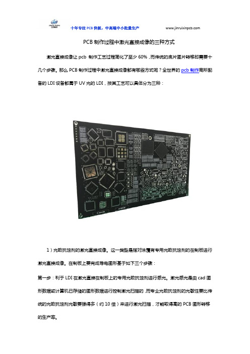
PCB制作过程中激光直接成像的三种方式激光直接成像让pcb制作工艺过程简化了至少60%,而传统的底片图片转移却需要十几个步骤。
那么PCB制作过程中激光直接成像都有哪些方式呢?全世界的pcb制作商所配备的LDI设备都属于UV光的LDI,按其工艺可以具体分为三种:1)光致抗蚀剂的激光直接成像。
这一类型是指对涂覆有专用光致抗蚀剂的在制板进行激光直接成像。
在制板上要完成导电图形基于如下三个步骤:第一步:利于LDI在激光直接在制板上的专用光致抗蚀剂进行感光。
激光感光是由cad图形数据或计算机已存储的图形数据进行控制激光扫描的,而专业光致抗蚀剂的光敏性要比传统的光致抗蚀剂光敏要强得多(约10倍)来进行激光扫描,才能取得高的PCB图形转移的生产率。
第二步:化学显影。
专用光致抗蚀剂仍采用传统的弱碱性碳酸钠溶液进行显影。
第三步:化学蚀刻。
由于专用的光致抗蚀剂是属于耐酸性(或则耐酸性强于耐碱性)的,因此要采用酸性氯化铜蚀刻溶液等来进行蚀刻。
2)pcb制作采用化学镀锡的激光直接成像。
在制板上化学镀锡的激光直接成像(LDI),某些文献又称为激光直接刻板。
这一类型是指在制板上利用化学方法镀上一层很薄的抗蚀层锡,然后利用激光蚀刻去不需抗蚀刻、保护的锡层及底下的部分厚度(3μm~5μm)的铜箔,然后进行化学蚀刻。
由于锡层在0.5μm~1.0μm厚度)是抗碱不耐酸的。
3)以覆铜箔的在制板上的激光直接成像,这一类型是指仅在覆铜箔在制板上的激光直接成像。
他不需要对在制板进行任何涂覆抗蚀保护层,而是直接利用激光蚀刻去不需要的铜箔,但是为了损伤介质厚度,往往还留下3μm~5μm厚度的铜箔,然后进行严格控制的快速化学蚀刻而出去留下的铜箔厚度。
因此在制板上的铜导体图形的铜厚度将会变薄些。
这具体问题具体分析。
综上所述我们了解到了PCB生产制作过程中使用的激光直接成像的类型方式,工艺在于精益求精,不断实践和优化提升。
深圳金瑞欣特种电路是专业的电路板打样和中小批量生产厂家,主营2-30层高多层板,、高频板、厚铜板、Hdi板等。
丝网印刷直接制版(CTS)激光成像技术及设备

丝网印刷直接制版(CTS)激光成像技术及设备激光技术介绍激光技术(见图1)的输出方式是由激光头产生光柱并进行曝光,曝光过程中把网版直接当作胶片。
激光曝光与喷墨制版的区别是激光成像使用激光而非油墨,从材料而言,即便宜又环保。
但激光曝光系统有一问题是需要专用感光胶,因为激光曝光的波段只有较窄的几个毫微米,曝光范围小,与感光范围在360nm~420mm内的传统感光胶的不匹配,所以只能使用专用感光胶。
这种系统在间接制网印版的工艺方面用的较多。
图2是激光曝光成像的主要技术环节。
图1 激光成像系统文 杨芳图2 Screen Setter成像系统(注:Reflector:反射镜;UV-lamp:UV灯;optical lens:光学镜头;DMD:数字微镜设备;Lens:镜头;stencil:网版。
)在激光成像制版中,也有人提出在非图文部分直接喷射感光胶再固化的方法,理由是这样就不需显影处理。
但是考虑到感光胶粘度、流动性、丝网网孔大小不同等因素,这种方法在实际操作中实用性不高,所以较少人去研究这种方法。
激光曝光系统除了CTS系统有的优点外,它的缺点就是对感光胶的使用要求比较严格。
这种技术最适用于每天重复使用同一种油墨在同一种介质上印刷的工作者。
Stencil Writer系统Stencil Writer系统由Berg Engneering公司生产,在1997年投入使用,它的应用主要集中于工业精细印刷和商业印刷。
此系统采用氩激光直接曝光成像,用于间接的丝印制版工艺(即先在感光片上形成镂空的图像,然后进行贴网的制版工艺)。
该系统配备了一款名为“Custom dot”的软件,能影印高质量、连续调的图像。
系统允许接受PC格式、MAC格式和Postscript level格式文件。
系统可达分辨率和速度分别为1270dpi和50%网点覆盖率10min 制1m2。
瑞士Safer公司提供的Safer LDS由于使用材料的恒定性,这种系统最受DVD 以及CD制造商的欢迎。
印刷制版中的激光技术应用的原理

印刷制版中的激光技术应用的原理激光技术在印刷制版中的应用原理主要包括激光光束的形成、激光光束的调制和激光光束的投射。
激光光束的形成是通过激光器产生的。
激光器通常由激光介质、泵浦源和光学谐振腔组成。
激光介质的种类有很多,如气体、液体或固体等。
当激光介质处于激发态时,外界的泵浦源(如电流、光、化学反应等)可以使其处于受激辐射的状态,进而激发介质分子向较低能级跃迁。
这种辐射过程是自发辐射和受激辐射的综合效果,它产生了具有高能量、高亮度和高方向性的激光光束。
光学谐振腔是一个能够反射激光光线的结构,它可以反射光线,并将它们反复通过激光介质,从而提高激光光束的放大程度。
最终,通过一系列的过程,激光器可以产生高功率的激光光束。
激光光束的调制是为了满足印刷制版的要求。
调制一般包括功率调制和空间调制。
功率调制是通过改变输入光束的功率来实现的,可以通过控制激光的泵浦源或激发介质的参数来调节,以获得所需的功率输出。
空间调制是指通过空间光调制器(如光栅、液晶等)改变激光光束的相位和振幅来实现,以进一步调试光束的特性。
这样可以将光束聚焦到一个确定的位置,以便在制版过程中更好地控制激光的能量分布。
激光光束的投射是通过合适的光学系统来实现的,以便将光束准确地投射到印刷制版的目标上。
投射一般需要满足激光光束的均匀性、稳定性和焦距等要求,以确保最终的印刷质量。
激光光束的均匀性通过调节光束形状(如圆形、方形等)和能量分布来实现。
光束的稳定性通过合理设计和调节光学系统的参数来实现。
焦距的调节是基于制版材料的类型和厚度来实现的,以实现所需的刻印或曝光效果。
除了激光技术在印刷制版中的基本原理外,还有一些与激光技术相关的辅助技术也在印刷制版中得到了应用。
例如,激光束的散斑技术可以通过调整激光光源和光学系统来消除激光光束的散斑效应,从而获得更好的印刷效果。
激光束的光谱分析和调控技术可以用于实时监测激光光束的性能,并根据需求进行调节,以获得更好的印刷质量。
直接成像技术在PCB中的应用
ad d vcsh as nf m t f c nterq l n eie a i ie et g i e o h umme t o teF B .d e ns fh C m 唧
. tec ̄ e f l o lc ma — As h c v n c cnati g i* ml
优 缺 点及 其在 P B制作 中的应 用。 C 关键 词 : 直接 成像技 术 ; 印制板 ; 成像原 理
中圈分 类号 :N 1 T 4
文 献标识 码 : A
文章编号 :01 4420 】2 6 —0 i0 —37(020 —03 3
Die tI 昏n c n lg o CB r c ma g Te h oo y frP
i i u tt dt tedm ns f i 4 ̄i t rste1 e r t H g( I t h o r s mas e o h e ad h出 esyp t , a r i c . 曲】 u)) e n l igo o g il o t ae n h s de m c  ̄ s odf r
CHEN n H UANG i d n Bi g, Zh — O g
( . hn i ut eh ooy( h no )C roain S atu 55 4 , ia 1 C iaCr i T cn lg S a tu op rt ,h no 10 1 Ch ) c o n
Ab tat sr c : ice s g d n rai d m柑 sh mil ̄r a o n 豇 r naxi 6 n ad z fn t nly d lc i c ̄ u c o ai i t e t er xn ns 3e t
激 光直接 成像 技 术( )用 于 P B业始 于 2 世 uI ) C 0
激光在印制电路板制造中应用的新进展

单 孔 逐 次 加 工 ,在 加 工 效 率 方 面 大 大 落 后 于 C O 激
光 钻 孔 ,一 般 CO, 光 钻 孔 的速 率 是 uV激 光 的4 5 激  ̄ 倍 [ 】 。同 时uV激 光 钻 孔 由于 可 以实 现 对 铜 和 介 质 基 材 的一 次 性 去 除 而不 需要 对 铜 面进 行 特 殊 处 理 , 因 此 在盲 孑 制 作 时 需要 钻 孔 参 数 的 精 确控 制 ,否 则 L 容 易 出现 盲 孔被 打 穿现 象 。 1 9 年 欧 文 等 人 发 现 94 在uv 激 光烧 蚀铜 时 , 由于铜 材对uV AG激光 的高 Y
余 介质层 并清 除孔 内残渣 ,第 三步利 用频 率非 常低 且 不伤害 底层 铜 的激光执 行L S 程 ,实现 了 非传统 工 A过
序 厚径 比11 :的盲T N作 ( 图2 。采 用L 机 制 进 L 如 ) AS
1. 4.
以波 大 于7 0n 6 m的 红外 光 将 有机 板 材 予 以 强热 熔 化
随着 新 型 高 敏 感干 膜材 料 等 研 发 的 不 断 成 熟 ,必 将 成 为 以后 微 影 制 程 技 术 的主 流 。 当前 和 今 后 的 一段 时 间里 ,要解 决P B中 “ 高密 度 ”导线 的精细 度 、 C 甚 位 置度和 层 间对位 问题 ,必 离不 开L I 术[。 D 技 4 】
一
[] 2 林金 堵 . 光 直接成 像 技术 ( I J. 激 V )[ 印制 电路信 1
息 , 0 23 2 0 ,.
[] 困龙 , 迪. 内激光 直接 成像 ( D )技术 发展 3张 马 国 LI
第六讲激光直接成像技术
(2)图形质量
LDI具有两个最突出的特点 1)能量高 高能量的光束对细导线形成起关键作用
在高能光照射下,这种激活的分子浓 度较低照度激活分子浓度高,当较多分 子处于激发态、抗蚀剂对光的吸收特性 就发生改变,光子可以轻易穿越到抗蚀 剂更深部位。使之整体更易聚合
(2)图形质量
2)光线直射板面 任何散射或非垂直光的照射都可能 引起成像区域外的抗蚀剂聚合反应 ,影响线条质量
4、直接成像的设备
2)较高的生产效率 对18英寸×24 英寸印制电路 板,达到每小时120面以上的 产能
4、直接成像的设备
3)好的可操作性 把 LDI设备设计得如同激光打印机 一样,数据处理部分设计合理
4、直接成像的设备
4)高可靠性 要求激光输出稳定、可靠,光源本 身具有较长的正常工作寿命,整套 光路的组成部分坚固,在高速移动 下保证定位准确
(1)紫外LDI专用抗蚀剂
2)工艺范围与质量 常规抗蚀剂用于LDI,难以确定它是否聚 合完全、极易出现影不足或过显影 常规干膜都有—层聚酯保护膜,若其中 含有少量不完全透明的微粒,在LDI中易 造成线条表面凹坑和侧壁效应
3)分类
LDI专用抗蚀剂分为干膜与液态两种 液态抗蚀剂除了运行成本低,适于 不平整的印制电路板表面等原有的 长处外,在 LDI 中表现最突出的特 点是其成膜很薄,可达8微米
提高细导线制造的合格率,避免重复缺 陷
3、直接成像的优点
尺寸稳定,定位精度提高
3、直接成像的优点
精确细导线的制造
3、直接成像的优点
缩短印制电路板制造流程,减少周 转时间
3、直接成像的优点
提高快速反应能力 ,降低生产成本, 减少不必要的损失
3、直接成像的优点
提升PCB性能的激光直接成像技术
Th s rDie tI a i g eLa e r c m g n
‘
T c n l g o I p o ePCB r o m a c e h o o yt m r v Pe f r n e
H U Zhiy n ・o g
Ab tac sr t
M a y‘ t n a d e in r lsf rr g sr to a ec n e o i c e s o r u c o aiy a n ‘ a d r ”d sg u e o e itai n c n b ha g d t n r a eb a d f n t n lt . nd s i
制 造 出各 种 类 型 的 P CB 组 件 。但 是 , 随 着 工 艺 技 术 的 不 断 改 进 , 设 计 师 应 该 知 道 他 们 提 供 的新 技
组 件 的 成 本 可 能 会 降 低 。LDI不 仅 是 一 种 制 造 微
细引线和很 多小尺寸产 品的工具 。在 P CB 的 制 造
生 产 中 ,它 是 唯 一 有 能 力 对 P CB 制 造 生 产 中 的 每
一
幅 图 片 进 行 单 独 登 记 记 录 和 按 比例 排 列 的 。 现
今 ,越 来 越 多 的 P B 公 司 在 生 产 过 程 中采 用 L C DI
技 术 。
PitdCi u fr t n 印制 电路 信 息 2 0 o … … . r e r iI omai n c tn o 08N . .
c s f ih e d C s o l cesdt og sr i ci g g(D )L ojsao lo k n e oto g -n B ud e erae ru hl e r tmai L I DIs t t o e ei s s h P c bd h a de n . in t t ma f l u i n
PCB全制作流程中的激光直接成像技术应用
PCB全制作流程中的激光直接成像技术应用Graph 1: trend of line & space at DYCONEX over the last 10 years The consequent use of LDI capability over the complete PCB manufacturing flowDaniel Schulze, Uwe KramerDYCONEX AGGrindelstrasse 408303 Bassersdorf, SwitzerlandT3.4 PCB QualityOral PresentationAbstractThe systematic implementation of optimized LDI (Laser Direct Imaging) photo resist types, LDI exposure units and fine line AOI (Automated Optical Inspection) equipment enhances the production technology and provides optimized PCB solutions for customers. This standardization results in a significantly faster and easier process flow with very precise registration. For high-reliability medical implants, full traceability can be obtained by adding individual serial numbers, date stamps and 2D barcodes for recording various process parameters.Design requirementsDriven by the assembly technology and analyzing the design requirements of the customers over the last 10 years a clear trend to smaller feature sizes is seen. A typical medical implantable product has afeature size of 50 μm line /space. Typical via diametersbetween 50 and 75 μm andpad sizes between 150 μm and 250 μm are standard tofind on these markets. Toassemble resistors of 0201packagingsizes will increase the requirements to the solder maskalignment as well down to25 μm alignment precision.During the quotation phase a detailed design rule check (DRC) has to be done to analyze customers design requirements. Dependent on these requirements like annular ring, layer to layer accuracy or solder mask to artwork accuracy the right registration systems have to be chosen to define the most cost effective and precise manufacturing flow.The graph below shows that the corresponding alignment accuracies are dependant on the customer design and finally used registration concept within the PCB manufacturing.Graph 3: registration concept dependant on customer design class using the annular ring as exampleGraph 2: typical misalignment failure modes Registration SystemsLaser via LDI Artwork Solder maskMechanical via LDI Artwork Solder maskPlasma via LDI Artwork Solder maskaverage compensationstep & repeat compensationaverage compensationindividual compensationindividual compensationindividual compensationindividual compensationaverage compensationaverage compensationaverage compensationaverage compensationEquipment requirementsThe challenge for PCB manufacturers is to constantly implement new manufacturing technologies to satisfy the customers growing demand in PCB complexity, cost efficiency and shorter delivery cycle times. In addition these requirements from the customers have to be linked to profitability of the supplier. Oneof the trends which has been observedduring the last years is the direct imagingtechnology. The growing market for directimaging tools reflects the increasingvariety of DI (Direct Imaging)technologies and vendors. Specializedsystems for different requirements are available. There are entry level systems,tools with double stage loading for faster throughput, high resolution systems and systems which cope with imaging of solder mask. All these systems offer a great variety of advantages over conventional film exposure which will be described in detail in the next chapters. Before starting with DI technology in production one needs to think about the specifications for the equipment. What should the tools be used for? What is the conversion strategy from film imaging to DI? Are there restrictions from customers which need to be addressed? Should and can the equipment operate in automated mode withoutoperator support? What advantages in detail are of interest for the production environment?Due to the demands of customers the requirements on DI systems are well defined. A film plotter has a resolution of 2.5 μm pixel size in comparison to a modern LDI with coherent light and 1 μm pixel size. Therefore LD I systems can offer resolutions higher than 20 μm line and space. Further requirements of the LDI equipment are registration performance better than 10 μm and programmable compensation schemes to include individual compensation together with step & repeat compensation. Furthermore, the systems need to be able to expose solder masks within a competitive process time. Customers are asking for full traceability during PCB manufacturing. Therefore, implementation of individual serial numbers, bar codes or date stamps during imaging is an important feature.After having defined all these prerequisites the process environment needs to be evaluated for matching the DI properties. Contrary to standard film foil exposure units most LDI systems use only one wavelength. Whenstarting with LDI processing inproduction photo resists are typicallynot optimized for direct imaging. Thismeans they either require longerexposure times compared to filmfoil Graph 4: film exposure and LDI exposure equipmentGraph 5: conventional exposure vs. LDI exposureexposure or they are not suitable at all for DI. Even if the standard photo resist can be exposed with DI the change to LDI optimized resists should be taken into account. Today there is a very big variety of optimized DI resists available on the market.After implementing these resists the cycle time for artwork imaging in comparison to film imaging is significantly reduced.Compared to photo resists conventional solder mask exposure requires much higher exposure energy; up to 800mJ/cm2. When establishing direct imaging processes in manufacturing this fact needs to be taken into account. Depending on other requirements the DI capacity needs to be calculated to be sufficient for conventional solder mask exposure. Optimized direct imaging tools are available on the market which combines both the advantages of direct imaging and the high exposure energy. The other option is to qualify new solder mask materials which are optimized for DI. As mentioned above the need for direct imaging of solder masks is usually given on very thin flex products. However, only a limited number of flexible solder masks are available. These solder masks can be exposed with less than 100mJ/cm2. Since medical customers can not change solder mask during the life cycle of a certified product a qualification of a solder mask for direct imaging is a long-term and strategic decision. Therefore at DYCONEX we have qualified two types of flex solder mask for direct imaging. When applying the solder mask optimized for direct imaging an exposure cycle time of less than 90 seconds per panel is achieved. In comparison to LDI solder mask, conventional solder mask exposure takes 6 times longer.Registration ConceptsSubstrate materials are changing in size during the various manufacturing steps. For example plating, desmearing or any process steps where heat is applied. Therefore a start compensation value is given to the substrates to accommodate for the shrinkage or expansion. Changing the single step artworkexposure to LDI has an influence on the rest of the manufacturing process steps. Conventional film foil exposure with just one single compensation value for the entire manufacturing lot as opposed to single panel compensation value to each individual panel using LDI. Thus the complete registration chain from the beginning of the first drilling step through to the artwork and solder mask exposure and ending up with the final routing has to be reviewed.One of the conventional registration concepts is to build sequential products and align layer to layer referring directly to the inner layer structure. A newer registration system uses x-ray drilling to reference to one or more inner layers at simultaneously. Changing from conventional multilayer registration concept to LDI offers several advantages: less process steps, faster through put time and higher alignment precision.The lower number of process steps in the work flow for LDI registration system is seen in Graph 6. For the conventional registration the reference system needs to be protected with 4stickers prior to plating. The punching of the reference system needs to be done. After that the compensation needs to be measured and the films need to be plotted. During exposure the film needs to be aligned to the panel and for good imaging performance vacuum needs to be applied. If required additional sets of films need to be plotted where compensation deviations within the work order occur. The exposure process itself is typically performed simultaneously on front and back of the panel. The overall process time including the supporting processes is 5 - 10 minutes per panel.For the LDI registration process the reference system can bedrilled and does not need to be protected. No film needs to be plotted and the individual compensation does not need to be measured in advance. The exposure of front and back is done sequentially. The overall process time including application of resist is less than 2 minutes per panel.Graph 6: comparison between conventional registration and LDI registration systemCompensation conceptsBasically within the film exposure process only an average compensation for the entire lot of multiple panels is possible. Depending on the LDI equipment used a variety of different compensation schemes can be applied:average compensationindividual panel compensationstep & repeat compensation (sub panel scaling)Step & repeat scaling can help when highcompensation offsets are present within a workorder. Individual compensation is not feasibledue to the following processes where onlyaverage compensation, like final mechanicalrouting or screen printing has been applied.The most accurate and at the same time mostcomplex scaling concept is the step and repeatregistration and compensation.Comparisons between different compensationschemes show the performance improvements.Very thin flex material tends to non linear distortions which occur through the entire manufacturing process. These distortions can not be compensated completely. All remaining distortions which can not be corrected are reflected in loss ofannular ring and misregistration. Together with the increasing complexity as mentioned in the beginning of this paper the annular ring requirements are also increasing. Today standard alignment requir ements are 25 μm for both artwork and solder mask. Typically thin flex material distortions within a workorder can be higher than 300 ppm. This can result, depending on panel size in more than 50 μm loss in annular ring.When film foil exposure is applied no kind of deviation can be corrected. When using individual panel scaling the panel to panel variation can be compensated. This reduces the amount of annular ring failures by a factor of two. The impact of the non linear distortions can Graph 8: material distortion within one single panelGraph 7: material distortion within a work order of multiple production panelsbe reduced when step & repeat registration is applied. Measurements on 25 μm flex material show that the registration within one workorder is improved again by a factor of two. The conclusion of this is that only DI systems can guarantee the high yields to satisfy increasing demands on high density PCB’s.When individual or step & repeat compensation is applied the same compensation methods should be applied to the following process steps. As an example the artwork and solder mask on a 25 μm thin flex panel is imaged using step & repeat compensation. This results in 25 μm registration accuracy. Nevertheless the distortions within a panel are higher than this. Therefore the final mechanical routing also has to be done with step & repeat compensation. Otherwise positioning failure of the PCB structures relative to the routing contour will occur. In other words, the full potential of individual or step & repeatcompensation needs to be considered for the entire process chain.Individual and step & repeat compensations in artwork imaging are well established in the PCB industry already. Same holds true for laser processing. Last but not least the solder mask imaging is the process which also needs to be converted to direct imaging.average compensation = x panel individual compensation = 1 panelS&R compensation = 1/x panelaverage compensation individual compensationS&R compensation Graph 10: registration performance depend on used registration conceptTraceability InformationAs mentioned above most customers ask for traceability of their products through the entire manufacturing process. Traceability means a unique numbering of the manufacturing lot, panel, delivery panel and print at least. This can mean bar codes and date stamp of customer specific counters. Since for DI process no film needs to be plotted, these features can be implemented directly during exposure. The individual features are etched in copper. The same can be done when solder mask is exposed with direct imaging. On some products a legend print is included. Even here the individual serial number can be exposed. At DYCONEX all artwork exposures enable individual serial numbers for full traceability.Graph 11: Traceability information with LDI exposure and copper etchedConclusionTo achieve higher yields and faster trough-put times achange from conventional manufacturing technologies like film exposure to advanced manufacturing processes like laser direct imaging is necessary for high-end, high-reliability flexible PCB’s in the medical, avionics or semiconductor market. T o use LDI exposure in PCB manufacturing requires several equipment updates. Changing the photo chemistry lines and implementing new photo resists or reference systems are just some examples. Following this path results in a new spectrum of smaller and more miniaturized PCB’s with the advantage of better alignment registration, higher accuracy, faster through put time and a better traceability.Manufacturer IDLot NumberPanel NumberPrin t Position NumberDate CodeCustomer Article Number 2D Barcodecopper etchedBiographyMr. Daniel Schulze studied at the Technical University of Dresden and has a diploma degree in Electrical Engineering. During his diploma thesis and an internship at the Georgia Tech Packaging Research Center he got involved with the work on optical waveguides embedded in PCB’s. In 2005 he started to work as Product Engineer at DYCONEX. Since 2008 he is Engineering Manager at DYCONEX and responsible for the product development of medical imaging PCB’s, hearing aids and cochlear implants, industrial and HF products.Mr. Uwe Kramer studied at the University of Halle/Wittenberg and the Technical University Dresden. He holdsa diploma degree in physics. He is specialized in semiconductor and metal physics. The diploma thesis was done in collaboration with Advanced Micro Devises and Fraunhofer Institute for Mechanics of Materials. Thesis of diploma was three dimensional reconstruction and analysis of grain structure by using fine beam techniques. Mr. Kramer joined DYCONEX in 2008 as process engineer. Since 2013 he is manager of the process module artwork and senior process engineer.。
pcb曝光ldi原理
pcb曝光ldi原理
PCB曝光LDI原理是指PCB(Printed Circuit Board,印刷电
路板)曝光时使用的LDI(Laser Direct Imaging,激光直接成像)技术。
LDI技术利用激光光源直接将PCB板上的图形信息转移到光
敏感材料上,从而形成所需的图案。
其原理包括以下几个步骤:
1. 准备光敏感材料,在PCB板上涂覆一层光敏感材料,通常是
光敏感的胶片或者光敏感的涂料。
2. 激光直接成像,LDI设备使用激光光源,通过光学系统将设
计好的图形信息直接投射到PCB板上覆盖的光敏感材料上。
激光照
射的位置会使光敏感材料发生化学或物理变化,形成所需的图案。
3. 图案显影,经过激光直接成像后,PCB板上的光敏感材料会
形成图案,接下来需要进行显影处理,将未曝光的部分去除,留下
所需的图案。
通过LDI技术,可以实现高精度、高效率的PCB曝光,避免了
传统曝光中使用光罩和化学显影的步骤,提高了生产效率和图形精度。
激光刻板技术——激光直接成像的新发展
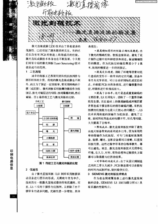
・
质 量信 誉 :S ⅢME NS作 为高质 量 的 电
子设 备制造商 ,已经成功地在全球范围推 出 70 多台 s 00 【 C MD贴片设 备, A ES 建立 了良
好 的 信 誉 。 激 光 直 接 制 板 设 备 在 德 国 ER IHS I同一生 产厂 制造 。 日1C A
有的检流计控制技术 , 以保护激光刻板的高 可 速进 行。加 之设 备 的光路设 计 简洁 , 保证 了激
光光 路的最 优途 径 和能量 的最小 损耗 。 光在 激 浸 锡层 上 的切 除 速度 可 以达 到每 秒钟 10 00毫
米。
・
先进 的激 光技 术 :S 伍 Ns的高频 钕 皿n
・
降低成 本 : 激光 直接 刻 板技 术除 了避免
由底 片制备带来 的 系列成 本 以外 ,因为采用简 单 的爱锡 作 为抗 蚀层 .对 专 门 的基材 表 面准 备、 贴膜 、 曝光 、 显影 设备都 可 以省略 , 以直接 刻板代 替 ,这些 过程 中带来 的合 格率损 失 ,都
可以避免。而且. 激光直接刻板技术无须净化
由f : 激光直接刻板 (s 同样采用数据驱 I) J 动设备进行图形的形成 ,无需底片作为中介 , 故而具有一般激光直接成像的所有优越性 。 而
且 , S 采用干 膜作 为抗蚀 剂 , 消除 了由干 L 不 又
有卓越的性能特点:
膜带来的诸多问题 , 优越性进一步增加 , 具体
维普资讯
激 光具有非 常 高的能 量密度 ,可以对锡层 进行 高速直接蚀 刻 。光学 回路 的设 计 非常简单 , 提 高激光传 输能量 效率 , 使得 光束定 位精确 。
・
直接成像技术在PCB中的应用
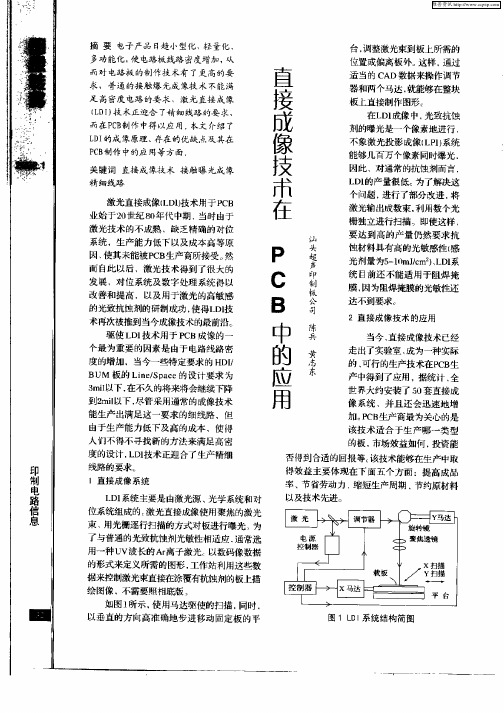
苎 竺 要 此 要 差 警 量 些萼 苎, 查 系 三粤 望 得
的光致抗蚀剂的研制成功 , 使得L I D技
I , 昂 、
一
不 适 磊 能用 磊 晶 菇 荏
~ “
司
…
…
’一
t f . 箭
由
路 信 息
_
以 … 方 准 步 u 定 _平 垂 的 高 确 进L Ⅲ H 直 … ‘ J 1K 固 板J 向… 移 地 动 , , 的
● 每年共节省照相底版费用为:20x 0
3H ¥ 0 ¥ ,0 , 1 ; Ilx 2 = 1 0( I 2 )
● 每年净节省费崩为 ¥2 H¨ l01 l【 x 8、 { I
¥l f“0 8 0 0 )=¥ 7 0 0 5
块板所需的时间大约为 l m n ,如果制作的 O is 是8 层板 , 这样就能节省3 m n , 6 is 除了节 省时
● 每天制作的菲林数为: 0 11=0 ; 20)( 2 0 / ̄ ● 每年 直 接 成 像 系 统 的操 作 成 本 :
¥ 5 0 0 100 ;
● 每年 lmJ O 的光致抗 蚀 剂成本 为 :sf ?qt ,
× ) 0s . 1 /qf 2 0 × 3 N= 1 00 0; t× 0 0 () ¥ 8 . 0
生产能 力较接触 印制有较大的提高 .运 用浚
技术使生产商有了更 多的选择 ,能获得更大
的经济效益。 该技术能 大大地减小盘 的尺寸 , 有效地利用基板面 , 从而缩小了板的尺寸 , 减
少 了板 的 层数
t nc G以及台湾的一些高技术P B r iA o C 生产商 均应用这一成像技术 , 以提 高高密度板 、 高层 板 、柔性板等的成 品率 ,从中获得较 大的利
第六讲激光直接成像技术
激光直接成像设备
4、直接成像的设备
(1)分类—按照光源 1)紫外激光直接成像 成熟的产品 ,设备多为平面台面, 单面曝光,采用紫外光敏感抗蚀剂 ,可在黄光下工作
(1)分类—按照光源
2)可见激光直接成像 只能在暗室或低照度红光下使用。 其波长位于488纳米,能源利用更加 有效,必须采用专用可见光抗蚀剂 3)YAG激光直接成像 可以在金属抗蚀涂层上进行选择性 蚀刻,不采用光致抗蚀剂
激光直接成像技术
金鸿
微电子工程系
印制电路板
印制电路板
印制电路板
多层印制板的制造工序有100多道,其 中图像转移是印制电路板生产过程中的 关键步骤
一、接触成像技术
接触成像技术在现代印制电路板制造 中有着多年的历史,接触成像技术需要照 相原版,并且曝光时生产底版与印制板必 须充分接触
1、接触成像工艺
4、直接成像的设备
2)较高的生产效率 对18英寸×24 英寸印制电路 板,达到每小时120面以上的 产能
4、直接成像的设备
3)好的可操作性 把 LDI设备设计得如同激光打印机 一样,数据处理部分设计合理
4、直接成像的设备
4)高可靠性 要求激光输出稳定、可靠,光源本 身具有较长的正常工作寿命,整套 光路的组成部分坚固,在高速移动 下保证定位准确
(2)图形质量
LDI具有两个最突出的特点 1)能量高 高能量的光束对细导线形成起关键作用
在高能光照射下,这种激活的分子浓 度较低照度激活分子浓度高,当较多分 子处于激发态、抗蚀剂对光的吸收特性 就发生改变,光子可以轻易穿越到抗蚀 剂更深部位。使之整体更易聚合Fra bibliotek (2)图形质量
2)光线直射板面 任何散射或非垂直光的照射都可能 引起成像区域外的抗蚀剂聚合反应 ,影响线条质量
激光技术在印制电路板行业的应用
激光技术在印制电路板行业的应用作者:宋金月来源:《科学与技术》2019年第21期摘要:激光直接成型(LDS)技术,指利用激光将数字化的图形照射到高分子材料表面,通过对照射过的区域进行直接金属化,最终在高分子材料表面形成图案的技术。
它可以在高分子壳体上直接形成金属化的图案。
本文详细探讨了LDS技术的原理、加工方法、应用方向、在印制电路板中的应用前景以及目前存在的应用缺陷。
关键词:激光技术;印制电路;应用引言:激光(Laser)是20世纪科技领域中与原子能、半导体及计算机齐名的4项重大发明之一。
50年来,激光技术发展异常迅猛。
以激光器为基础的激光技术在我国得到了迅速的发展,现已广泛用于工业生产、通信、信息处理、医疗卫生、军事、文化教育以及科学研究等各个领域。
随着电子产品朝着多功能、便携式、小型化的方向发展,对印制电路板高密度化和小型化提出了越来越高的需求。
提高印制板高密度化水平的关键在于越来越窄的线宽、线距和越来越小的层间互连孔直径、连接盘,以及严格的尺寸精度,于是激光技术被引入印制板加工中。
一、概述关于激光的起源,最早还要追溯到科学家爱因斯坦,爱因斯坦在上世纪初就提出了受激辐射的理念。
随后,上世纪中期,美国微波领域的著名科学家肖洛和汤斯发表了关于“红外与光学激射器”的论文,全文明确阐述了受激辐射发光的可能性,同时也阐述了受激辐射发光的条件――“粒子数反转”。
1960年,美国科学家梅曼成功发明了一台世界上最早的红宝石激光器。
至此,激光和激光技术开始了迅猛的发展。
而我国的第一台激光器是在王志江院士的主持之下于1961年成功制造出来的。
而关于我国的激光和激光技术起源,主要还是受到国外的影响。
但是激光技术自从在我国起源就得到了良好的发展,无论是发展成果的质量还是数量都与世界水平差异不大。
二、激光技术组成和特性(一)激光器的主要组成结构经过多年的发展和完善,激光器的主要结构已基本定型,主要由三个部分共同组成。
pcb内光成像流程
pcb内光成像流程下载温馨提示:该文档是我店铺精心编制而成,希望大家下载以后,能够帮助大家解决实际的问题。
文档下载后可定制随意修改,请根据实际需要进行相应的调整和使用,谢谢!并且,本店铺为大家提供各种各样类型的实用资料,如教育随笔、日记赏析、句子摘抄、古诗大全、经典美文、话题作文、工作总结、词语解析、文案摘录、其他资料等等,如想了解不同资料格式和写法,敬请关注!Download tips: This document is carefully compiled by theeditor. I hope that after you download them,they can help yousolve practical problems. The document can be customized andmodified after downloading,please adjust and use it according toactual needs, thank you!In addition, our shop provides you with various types ofpractical materials,such as educational essays, diaryappreciation,sentence excerpts,ancient poems,classic articles,topic composition,work summary,word parsing,copy excerpts,other materials and so on,want to know different data formats andwriting methods,please pay attention!PCB 内光成像流程是 PCB 制造过程中的一个重要环节,它主要包括以下几个步骤:1. 底片制作设计 PCB 版图,确定电路布局和走线。
PCB制作中成像和电路制作的方式
PCB制作中成像和电路制作的方式王起;杨亚敏;王力文【摘要】对多个图像进行转移是PCB制作中图像成像的重最工作,也是PCB制作的重要内容。
一般的,在进行图形转移制作中使用CAD技术,或者使用钻通孔,钻微孔图像,或者通过构建内层电路图像和外层电路图像,或者构建抗蚀层等步骤来完成。
PCB电路的制作也是PCB制作中的重点内容,电路一般通过光刻或者是通过丝网印刷,为了做好电路的制程,要对材料进行不同程度的蚀刻,电镀和抗蚀层剥离等操作。
本文对半加成工艺和加成工艺,激光成像的选择,喷墨,投影进行分析探究,这对完善PCB制作具有积极的作用。
【期刊名称】《电子制作》【年(卷),期】2015(0)8Z【总页数】1页(P1-1)【关键词】图形转移;喷墨;激光;PCB【作者】王起;杨亚敏;王力文【作者单位】天水生产力促进中心【正文语种】中文【中图分类】TN41PCB技术已经得到了较好的发展,也已经取得了较好成效,目前在PCB制作领域出现了很对的新的制程,本文针对一些有代表性的制程进行了分析。
在PCB创新领域上已经应用了很多的技术,本文针对某些未成功的技术进行了适当的分析研究,本文还介绍了PCB制造中常见的喷墨和激光应用。
1.1 半加成工艺首先对半加成工艺进行简单的介绍,首先要制造种子层并将电解铜渡到平坦的表面上,然后为了增加表面的美观性,接下来要在抗蚀层上绘制图案,在这一步还要做好一下三个方面的工作,第一,溅镀铜到平坦表面上,第二,积层薄铜箔到平坦表面,第三,积层厚铜箔到平坦表面然后整体蚀刻减薄。
做好上面的工作之后进行图形电镀,之后进行抗蚀层剥离,最后进行差分蚀刻去除基铜。
上面制程是FC也就是先进倒装封装常用的电路形成过程。
一般的在较为平坦的介质层上进行无电镀铜渡,微通孔孔壁上一般也进行该操作。
制作抗蚀图像之后,根据这个图像的图案进行铜渡,紧接着将抗蚀层去除,然后将没用进行电镀的基层铜去除,在进行该操作的过程中使用差分蚀刻的方法,因为去掉了金属抗蚀层,所以电路虽然经过了电镀,但是仍然没有保护。
激光成像技术在制造业中的应用
激光成像技术在制造业中的应用激光技术是现代制造业中应用最广泛的一种先进制造技术,其应用领域广泛,尤其在激光成像技术方面,不仅解决了工业生产的一系列问题,同时也在材料加工、检测等领域中获得了极大的成功。
本文将探讨激光成像技术在制造业中的应用。
一、什么是激光成像技术激光成像技术是一种将激光作为光源进行成像的技术,该技术主要通过控制激光的位置、强度、时间等参数,对物体进行非接触式成像。
激光成像技术可应用于工业生产中的精密检测、零部件加工、信息存储等方面。
同时,该技术由于其非接触式成像的特点,还可以应用于卫星观测、医学成像等领域。
二、激光成像技术在制造业中的应用1、激光切割技术激光切割技术是利用激光束对金属材料进行切割,是目前制造业中最常用的加工过程之一。
激光能够对材料进行精确切割,适用于各种形状和大小的工件,并可以实现高速无损切割,提高了制造的效率和精度。
2、激光打标技术激光打标技术是通过激光束对材料进行标记、刻画的一种技术。
这种技术利用激光束在材料表面加工出有意义的标记,可以用于制品品牌标签、二维码、标识代码等方面。
这种技术具有速度快、精度高、效率高、可读性好等优点,因此被广泛应用于生产和质量控制领域。
3、激光焊接技术激光焊接技术是指通过控制激光的强度、聚焦距离等参数,在熔化双方材料的情况下进行物质的结合,从而达到焊接的目的。
这种技术适用于各种金属和塑料材料的连接和组装,并且可以实现高精度、高质量的焊接效果,被广泛应用于汽车制造、机械制造等领域。
4、激光表面处理技术激光表面处理技术是一种通过激光束对金属表面进行加工、改变其表面特性、改良其性能的技术。
该技术可以改变材料的表面形态、耐磨性、抗腐蚀性、抗氧化性等性能,可以使材料表面具有更好的物理和化学性能。
因此,这种技术在航空航天、电子制造、汽车制造等领域中都得到了广泛的应用。
三、结语激光成像技术在制造业中的应用越来越广泛,不仅提高了生产效率,同时也大大提升了制造品质和精度。
基于激光直写电路技术的PCB板快速制造系统
基于激光直写电路技术的PCB板快速制造系统徐璞【摘要】生产样品PCB板通常需要几天到1周的时间,这种较长时间的生产周期,不利于新产品研发时的快速验证.为了解决样品PCB板生产周期较长的问题,现有一种PCB板快速制造系统,可以实现在1天之内完成样品PCB板的制造.该系统的工艺步骤如下:钻孔及金属化孔→线路图形制作→阻焊图形制作→字符图形制作→助焊防氧化处理.该套系统能实现的加工能力为:最小孔径0.2 mm,最小线宽2 mil,线间最小间距0.8 mil,加工精度±0.08 mil.利用激光直写电路技术,该系统进一步解决了物理雕刻方式制作线路图形精度不够的问题,且在加工线路图形时对材料的热冲击效应较小,所以对加工精细间距的电路和射频微波电路有更好的效果,可有效解决高精度PCB样品板的快速制造问题.【期刊名称】《新技术新工艺》【年(卷),期】2019(000)003【总页数】5页(P58-62)【关键词】PCB;新产品研发;生产周期;快速制造;激光直写电路;线路图形【作者】徐璞【作者单位】重庆会凌电子新技术有限公司,重庆 401336【正文语种】中文【中图分类】TN41研发新的电子产品,需要经过产品设计、生产加工和调试等工序,其中,PCB板的设计、制造是最关键的环节之一。
大多数的元器件都可以在市场上采购到成品,而PCB板必须根据不同的产品进行相应的设计、制造;因此,PCB板设计、制造的周期长短对新产品的研发周期有着较大影响。
目前,按照PCB板生产厂的生产工艺,即使只生产1块样品PCB板,也和生产大批量PCB板的工艺流程一样,需要进行数据准备、光绘、下料、钻孔、金属化孔、贴膜或网印、曝光、图形电镀、蚀刻、阻焊涂覆、喷锡、丝印字符、外型加工和清洗等数十道工序[1]。
在这种生产模式下,从设计方和PCB板生产厂家确认PCB板设计文件开始,到最终完成PCB板的制造,通常至少需要几天到1周的时间。
这种工艺能满足批量产品的生产周期需要,但并不适合生产样品PCB板。
- 1、下载文档前请自行甄别文档内容的完整性,平台不提供额外的编辑、内容补充、找答案等附加服务。
- 2、"仅部分预览"的文档,不可在线预览部分如存在完整性等问题,可反馈申请退款(可完整预览的文档不适用该条件!)。
- 3、如文档侵犯您的权益,请联系客服反馈,我们会尽快为您处理(人工客服工作时间:9:00-18:30)。
Graph 1: trend of line & space at DYCONEX over the last 10 years The consequent use of LDI capability over the completePCB manufacturing flowDaniel Schulze, Uwe KramerDYCONEX AGGrindelstrasse 408303 Bassersdorf, SwitzerlandT3.4 PCB QualityOral PresentationAbstractThe systematic implementation of optimized LDI (Laser Direct Imaging) photo resist types, LDI exposure units and fine line AOI (Automated Optical Inspection) equipment enhances the production technology and provides optimized PCB solutions for customers. This standardization results in a significantly faster and easier process flow with very precise registration. For high-reliability medical implants, full traceability can be obtained by adding individual serial numbers, date stamps and 2D barcodes for recording various process parameters.Design requirementsDriven by the assembly technology and analyzing the design requirements of the customers over the last 10 years a clear trend to smaller feature sizes is seen. A typical medical implantable product has afeature size of 50 µm line /space. Typical via diametersbetween 50 and 75 µm andpad sizes between 150 µm and 250 µm are standard tofind on these markets. Toassemble resistors of 0201packagingsizes will increase the requirements to the solder maskalignment as well down to25 µm alignment precision.During the quotation phase a detailed design rule check (DRC) has to be done to analyze customers design requirements. Dependent on these requirements like annular ring, layer to layer accuracy or solder mask to artwork accuracy the right registration systems have to be chosen to define the most cost effective and precise manufacturing flow.The graph below shows that the corresponding alignment accuracies are dependant on the customer design and finally used registration concept within the PCB manufacturing.Graph 3: registration concept dependant on customer design class using the annular ring as exampleGraph 2: typical misalignment failure modes Registration SystemsLaser via LDI Artwork Solder maskMechanical via LDI Artwork Solder maskPlasma via LDI Artwork Solder maskaverage compensationstep & repeat compensationaverage compensationindividual compensationindividual compensationindividual compensationindividual compensationaverage compensationaverage compensationaverage compensationaverage compensationEquipment requirementsThe challenge for PCB manufacturers is to constantly implement new manufacturing technologies to satisfy the customers growing demand in PCB complexity, cost efficiency and shorter delivery cycle times. In addition these requirements from the customers have to be linked to profitability of the supplier. Oneof the trends which has been observedduring the last years is the direct imagingtechnology. The growing market for directimaging tools reflects the increasingvariety of DI (Direct Imaging)technologies and vendors. Specializedsystems for different requirements are available. There are entry level systems,tools with double stage loading for faster throughput, high resolution systems and systems which cope with imaging of solder mask. All these systems offer a great variety of advantages over conventional film exposure which will be described in detail in the next chapters. Before starting with DI technology in production one needs to think about the specifications for the equipment. What should the tools be used for? What is the conversion strategy from film imaging to DI? Are there restrictions from customers which need to be addressed? Should and can the equipment operate in automated mode without operator support? What advantages in detail are of interest for the production environment?Due to the demands of customers the requirements on DI systems are well defined. A film plotter has a resolution of 2.5 µm pixel size in comparison to a modern LDI with coherent light and 1 µm pixel size. Therefore LDI systems can offer resolutions higher than 20 µm line and space. Further requirements of the LDI equipment are registration performance better than 10 µm and programmable compensation schemes to include individual compensation together with step & repeat compensation. Furthermore, the systems need to be able to expose solder masks within a competitive process time. Customers are asking for full traceability during PCB manufacturing. Therefore, implementation of individual serial numbers, bar codes or date stamps during imaging is an important feature.After having defined all these prerequisites the process environment needs to be evaluated for matching the DI properties. Contrary to standard film foil exposure units most LDI systems use only one wavelength. Whenstarting with LDI processing inproduction photo resists are typicallynot optimized for direct imaging. Thismeans they either require longerexposure times compared to filmfoil Graph 4: film exposure and LDI exposure equipmentGraph 5: conventional exposure vs. LDI exposureexposure or they are not suitable at all for DI. Even if the standard photo resist can be exposed with DI the change to LDI optimized resists should be taken into account. Today there is a very big variety of optimized DI resists available on the market. After implementing these resists the cycle time for artwork imaging in comparison to film imaging is significantly reduced.Compared to photo resists conventional solder mask exposure requires much higher exposure energy; up to 800mJ/cm2. When establishing direct imaging processes in manufacturing this fact needs to be taken into account. Depending on other requirements the DI capacity needs to be calculated to be sufficient for conventional solder mask exposure. Optimized direct imaging tools are available on the market which combines both the advantages of direct imaging and the high exposure energy. The other option is to qualify new solder mask materials which are optimized for DI. As mentioned above the need for direct imaging of solder masks is usually given on very thin flex products. However, only a limited number of flexible solder masks are available. These solder masks can be exposed with less than 100mJ/cm2. Since medical customers can not change solder mask during the life cycle of a certified product a qualification of a solder mask for direct imaging is a long-term and strategic decision. Therefore at DYCONEX we have qualified two types of flex solder mask for direct imaging. When applying the solder mask optimized for direct imaging an exposure cycle time of less than 90 seconds per panel is achieved. In comparison to LDI solder mask, conventional solder mask exposure takes 6 times longer.Registration ConceptsSubstrate materials are changing in size during the various manufacturing steps. For example plating, desmearing or any process steps where heat is applied. Therefore a start compensation value is given to the substrates to accommodate for the shrinkage or expansion. Changing the single step artwork exposure to LDI has an influence on the rest of the manufacturing process steps. Conventional film foil exposure with just one single compensation value for the entire manufacturing lot as opposed to single panel compensation value to each individual panel using LDI. Thus the complete registration chain from the beginning of the first drilling step through to the artwork and solder mask exposure and ending up with the final routing has to be reviewed.One of the conventional registration concepts is to build sequential products and align layer to layer referring directly to the inner layer structure. A newer registration system uses x-ray drilling to reference to one or more inner layers at simultaneously. Changing from conventional multilayer registration concept to LDI offers several advantages: less process steps, faster through put time and higher alignment precision.The lower number of process steps in the work flow for LDI registration system is seen in Graph 6. For the conventional registration the reference system needs to be protected with4stickers prior to plating. The punching of the reference system needs to be done. After that the compensation needs to be measured and the films need to be plotted. During exposure the film needs to be aligned to the panel and for good imaging performance vacuum needs to be applied. If required additional sets of films need to be plotted where compensation deviations within the work order occur. The exposure process itself is typically performed simultaneously on front and back of the panel. The overall process time including the supporting processes is 5 - 10 minutes per panel.For the LDI registration process the reference system can be drilled and does not need to be protected. No film needs to be plotted and the individual compensation does not need to be measured in advance. The exposure of front and back is done sequentially. The overall process time including application of resist is less than 2 minutes per panel.Graph 6: comparison between conventional registration and LDI registration systemCompensation conceptsBasically within the film exposure process only an average compensation for the entire lot of multiple panels is possible. Depending on the LDI equipment used a variety of different compensation schemes can be applied:• average compensation• individual panel compensation• step & repeat compensation (sub panel scaling)Step & repeat scaling can help when highcompensation offsets are present within a workorder. Individual compensation is not feasibledue to the following processes where onlyaverage compensation, like final mechanicalrouting or screen printing has been applied.The most accurate and at the same time mostcomplex scaling concept is the step and repeatregistration and compensation.Comparisons between different compensationschemes show the performance improvements.Very thin flex material tends to non linear distortions which occur through the entire manufacturing process. These distortions can not be compensated completely. All remaining distortions which can not be corrected are reflected in loss of annular ring and misregistration. Together with the increasing complexity as mentioned in the beginning of this paper the annular ring requirements are also increasing. Today standard alignment requirements are 25 µm for both artwork and solder mask. Typically thin flex material distortions within a workorder can be higher than 300 ppm. This can result, depending on panel size in more than 50 µm loss in annular ring.When film foil exposure is applied no kind of deviation can be corrected. When using individual panel scaling the panel to panel variation can be compensated. This reduces theamount of annular ring failures by a factor of two. The impact of the non linear distortions can Graph 8: material distortion within one single panelGraph 7: material distortion within a work order of multiple production panelsbe reduced when step & repeat registration is applied. Measurements on 25 µm flex material show that the registration within one workorder is improved again by a factor of two. The conclusion of this is that only DI systems can guarantee the high yields to satisfy increasing demands on high density PCB’s.When individual or step & repeat compensation is applied the same compensation methods should be applied to the following process steps. As an example the artwork and solder mask on a 25 µm thin flex panel is imaged using step & repeat compensation. This results in 25 µm registration accuracy. Nevertheless the distortions within a panel are higher than this. Therefore the final mechanical routing also has to be done with step & repeat compensation. Otherwise positioning failure of the PCB structures relative to the routing contour will occur. In other words, the full potential of individual or step & repeat compensation needs to be considered for the entire process chain.Individual and step & repeat compensations in artwork imaging are well established in the PCB industry already. Same holds true for laser processing. Last but not least the solder mask imaging is the process which also needs to be converted to direct imaging.average compensation = x panel individual compensation = 1 panelS&R compensation = 1/x panelaverage compensation individual compensationS&R compensation Graph 10: registration performance depend on used registration conceptTraceability InformationAs mentioned above most customers ask for traceability of their products through the entire manufacturing process. Traceability means a unique numbering of the manufacturing lot, panel, delivery panel and print at least. This can mean bar codes and date stamp of customer specific counters. Since for DI process no film needs to be plotted, these features can be implemented directly during exposure. The individual features are etched in copper. The same can be done when solder mask is exposed with direct imaging. On some products a legend print is included. Even here the individual serial number can be exposed. At DYCONEX all artwork exposures enable individual serial numbers for full traceability.Graph 11: Traceability information with LDI exposure and copper etchedConclusionTo achieve higher yields and faster trough-put times a change from conventional manufacturing technologies like film exposure to advanced manufacturing processes like laser direct imaging is necessary for high-end, high-reliability flexible PCB’s in the medical, avionics or semiconductor market. To use LDI exposure in PCB manufacturing requires several equipment updates. Changing the photo chemistry lines and implementing new photo resists or reference systems are just some examples. Following this path results in a new spectrum of smaller and more miniaturized PCB’s with the advantage of better alignment registration, higher accuracy, faster through put time and a better traceability.Manufacturer IDLot NumberPanel NumberPrin t Position NumberDate CodeCustomer Article Number 2D Barcodecopper etchedBiographyMr. Daniel Schulze studied at the Technical University of Dresden and has a diploma degree in Electrical Engineering. During his diploma thesis and an internship at the Georgia Tech Packaging Research Center he got involved with the work on optical waveguides embedded in PCB’s. In 2005 he started to work as Product Engineer at DYCONEX. Since 2008 he is Engineering Manager at DYCONEX and responsible for the product development of medical imaging PCB’s, hearing aids and cochlear implants, industrial and HF products.Mr. Uwe Kramer studied at the University of Halle/Wittenberg and the Technical University Dresden. He holds a diploma degree in physics. He is specialized in semiconductor and metal physics. The diploma thesis was done in collaboration with Advanced Micro Devises and Fraunhofer Institute for Mechanics of Materials. Thesis of diploma was three dimensional reconstruction and analysis of grain structure by using fine beam techniques. Mr. Kramer joined DYCONEX in 2008 as process engineer. Since 2013 he is manager of the process module artwork and senior process engineer.。