TFTLCD驱动模块说明SPI
驱动IC介绍(TFT-LCD).
補償電壓:補償gate driver輸出電壓關閉時因為 feed through的關係顯示電極的電壓受到影響
9
雙脈波三階驅動
OUT 1
OUT 2
提供愈來愈高的解析度需求
預將電壓充到一定準位 減少真正充電時所需的時間
10
Gate driver framework
Output Ckts Level shifter
以便各個輸出的取樣暫存器能從Data bus上抓到 相對應的資料 Data input種類: CMOS, RSDS, LVDS 為了降低驅動晶片的工作頻率,常見的S Driver都採用雙畫素輸入,單畫素輸出的Driver 一次送出的顯示資料是三筆分別送到3個不同的 channel ,同理雙畫素輸入的Driver,為6個輸出 為一組。
32
Gamma電壓
Gamma 1 Gamma 2 Gamma 3 Gamma 4 Gamma 5
Common Gamma 6
Gamma 7 Gamma 8 Gamma 9 Gamma 10
00
40
80
FF
33
N TO 1 Selector
N TO 1 Selector的主要功能?
以6 bit source driver來說,一般外部的參 考電壓只有5到9組,經由N TO 1 Selector 內部的電阻分壓成64灰階用的參考電壓, 且由hold register送來的data控制所有的開 關電路。
28
Dual
Clock SPI Data R 1
………… …………
Data G 1
Data B 1
Data R 2
………… …………
…………
Data G 2
TFTLCD显示原理及驱动介绍
TFTLCD显示原理及驱动介绍TFTLCD是一种液晶显示技术,全称为Thin Film Transistor Liquid Crystal Display,即薄膜晶体管液晶显示器。
它是目前应用最广泛的显示器件之一,被广泛应用在电子产品中,如手机、平板电脑、电视等。
TFTLCD显示屏是由数百万个像素点组成的,每个像素点又包含红、绿、蓝三个亚像素。
这些像素点由一层薄膜晶体管(TFT)驱动。
薄膜晶体管是一种微型晶体管,位于每个像素点的背后,用来控制液晶材料的偏振状态。
当电流通过薄膜晶体管时,液晶分子会受到电场的影响,从而改变偏振方向,使光线在通过液晶层时发生偏转,从而改变像素点的亮度和颜色。
TFTLCD显示屏需要配备驱动电路,用来控制TFT晶体管的电流,以控制液晶分子的偏振状态。
驱动电路通常由一个控制器和一组电荷泵组成。
控制器负责接收来自外部的指令,通过电荷泵为晶体管提供适当的电流。
电荷泵可以产生高电压和低电压,从而控制液晶分子的偏振状态。
控制器通过一组驱动信号,将指令传递给TFT晶体管,控制像素点的亮度和颜色。
TFTLCD驱动器是用来控制TFTLCD显示屏的硬件设备,通常与控制器紧密连接。
驱动器主要负责将控制器发送的信号转换为液晶的电流输出,实现对像素点的亮度和颜色的控制。
驱动器还负责控制像素点之间的互动,以实现高质量的图像显示。
1.扫描电路:负责控制像素点的扫描和刷新。
扫描电路会按照指定的频率扫描整个屏幕,并刷新像素点的亮度和颜色。
2.数据存储器:用于存储显示数据。
数据存储器可以暂时保存控制器发送的图像数据,以便在适当的时候进行处理和显示。
3.灰度调节电路:用于调节像素点的亮度。
通过调节像素点的电流输出,可以实现不同的亮度效果。
4.像素点驱动电路:负责控制像素点的偏振状态。
像素点驱动电路会根据控制器发送的指令,改变液晶分子的偏振方向,从而改变像素点的亮度和颜色。
5.控制线路:用于传输控制信号。
控制线路通常由一组电线组成,将控制器发送的信号传输到驱动器中,以控制整个显示过程。
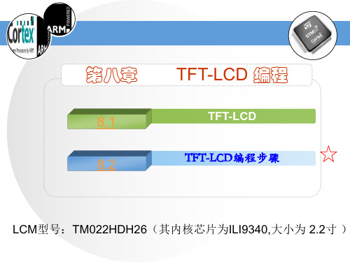
第八章 TFT-LCD编程2.2寸天马原装串口 TFT SPI 液晶屏模块 高清240X320 兼容5110
在 3.1版本固件库中:font.h 在目录 \STM32F10x_StdPeriph_Lib_V3.10\Utilities\STM32_EVAL中。 在 3.4.5版本固件库中:font.h 在目录 \STM32F10x_StdPeriph_Lib_V3.5.0\Utilities\STM32_EVAL \Common中。
TFT-LCD 编程步骤
显示字符
8.2
TFT-LCD 编程步骤
显示字符
1、字符的字模 2、加入头文件 3、延时初始化 4、LCD初始化 5、LCD清屏 6、点亮液晶屏(若用GPIO管脚 接 LCD背光正极)
(若用3.3V电压 直接接 LCD背光正极:无需要此步)
7、设置光标位置,显示字符
1、字符的字模
}
STM32F10x
②初始化LCD模块(即设置LCD工作模式)
①设置与LCD相连的 STM32管脚
void SPI1_Init(void) { SPI_InitTypeDef SPI_InitStructure; GPIO_InitTypeDef GPIO_InitStructure; //配置SPI1管脚 RCC_APB2PeriphClockCmd(RCC_APB2Periph_AFIO|RCC_APB2Peri ph_GPIOA, ENABLE); GPIO_InitStructure.GPIO_Pin = LCD_SCL | LCD_SDA; GPIO_InitStructure.GPIO_Speed = GPIO_Speed_50MHz; GPIO_InitStructure.GPIO_Mode = GPIO_Mode_AF_PP; GPIO_Init(LCD_CTRL, &GPIO_InitStructure); GPIO_InitStructure.GPIO_Pin = LCD_SDO ; GPIO_InitStructure.GPIO_Mode = GPIO_Mode_IPU; GPIO_InitStructure.GPIO_Speed = GPIO_Speed_50MHz; GPIO_Init(LCD_CTRL, &GPIO_InitStructure); GPIO_InitStructure.GPIO_Pin = LCD_LED |LCD_RS | LCD_CS| LCD_RST ; GPIO_InitStructure.GPIO_Speed = GPIO_Speed_50MHz; STM32F10x GPIO_InitStructure.GPIO_Mode = GPIO_Mode_Out_PP;
1.8寸LCD模块用户手册说明书
1.8inch LCD ModuleUSER MANUALOVERVIEWThis product is 1.8inch resistive screen module with resolution 128x160. It has internal controller and uses SPI interface for communication. It has already basic functions: setting the point size, the line thickness, drawing circle, rectangle, and displaying English characters.We provide Raspberry Pi, STM32 and Arduino routines for this product.FEATURESDisplay type: TFTInterface: SPIDriver: ST7735SColors: 256KResolution: 128 x 160 (Pixel)Product size: 56.5 x 34(mm)Display size: 35.4(W) x 28.03(H)(mm)Pixel size: 0.219(W) x 0.219(H)(MM)Operating temperature: -30°C ~ 85°CINTERFACE DESCRIPTIONMarking Description3V3 3.3V powerGND groundDIN SPI data inputCLK SPI clockCS chip selectDC data/commandRST resetBL back lightPROGRAM ANALYSIS1.Working principles:ST7735S is 132 x 162 pixels LCD panel, but the product is 128 x 160 pixels LCD display.In the display there are two processes: the horizontal direction scanning – from the 2nd pixel, the vertical direction scanning – from the 1st pixel. So, you can see that positions of pixels in RAM correspond to their actual positions while displaying.The LCD supports 12-bit, 16-bit and 18-bit per pixel input formats. They correspond to RGB444, RGB565 and RGB666 color formats. This routine uses the RGB565 color format, which is commonly used.LCD uses 4-wired SPI communication interface, which can save a lot of GPIO ports and provides fast data transfer to LCD as well.munication protocolNote: there is a difference from traditional SPI. Here we only need display, so sine wires come from slave to host are hidden. The detailed information please refer to datasheet at page 58RESX: Reset. Pull-down while powering on the module. Generally set as 1IM2: data communication mode pin, which define usage of SPICSX: chip selection control pin. If CS=0 – the chip is selectedD/CX: data/command control pin, if DC=0 – command is written, otherwise – data are writtenSDA: transmitted RGB dataSCL: SPI clockThe SPI communication protocol of the data transmission uses control bits: clock phase (CPHA) and clock polarity (CPOL):The value of CPOL determines the level when the serial synchronous clock is in idle state. CPOL=0, that its idle level is 0.The value of CPHA determines the timing of the data bits relative to the clock pulses. CPHA=0, data is sampled at the first clock pulse edge.The combination of these two parameters provides 4 modes of SPI data transmission. The commonly used is SPI0 mode, it is that GPOL=0 and CPHA=0.From the figure above, SCLK begins to transfer data at the first falling edge. 8 bits data are transferred at one clock period. Use SPI0 mode, High bits transfer first, and LOW bits following. DEMO CODERaspberry Pi, STM32 and Arduino programs are provided, wherein Raspberry Pi provides BCM2835, WiringPi and python programs. It implements common graphical functions as drawing dot, line, rectangle, circle, setting their sizes and line with; filling arias, and displaying English characters of 5 common fonts and other display’s functions.Following instructions are offered for you convenienceRASPBERRY1.Hardware connection1.8inch LCD module Raspberry Pi3.3V 3.3VGND GNDDIN MOSI (PIN 19)CLK SCLK (PIN23)CS CE0 (PIN 8)DC GPIO.6 (PIN 22)RST GPIO.2 (PIN13)BL GPIO.5 (PIN18)2.Enable SPI function of the Raspberry Pisudo raspi-configSelect: Advanced Options -> SPI -> yesActivate SPI hardware driver.3.Installation of librariesFore detailed information about libraries installation, please refer to this page:https:///wiki/Libraries_Installation_for_RPiIt is description of WiringPi, bcm2835 and python libraries installation.ageBCM2835 and WiringPi program should be only copied into directory of Raspberry Pi ()by samba or directly copy to the SD card). The following code are compied directly to the user directory of Pi.4.1Usage of BCM2835Run ls command as you can see below:bin: contains “.o” files.We don’t need to change it generallyFonts: contains 5 commonly used fontsPic: contains pictures used for displaying. The resolution of pictures must be 128x128,otherwise they cannot be displayed properly. And the format of pictures must be BMP.Obj: contains object files, like main.c, LCD_Driver.c, DEV_Config.c, LCD_GUI.c and theirheader files.main.c: The mian function. What need to note is that even though there are LCD_ScanDir used to control the direction of scanning, you need not to change it. Because this module is designed for Raspberry Pi, and for compatibility, we don’t recommend you to change it.DEV_Config.c:Definations of Raspberry Pi’s pins and the communication mode.LCD_Driver.c: Drive code of LCD. Need not change generally.LCD_BMP.c: Reading and analyzing BMP files and display themMakefile: This file contains compilation rules. If there are some changes in code, please run make clean to clean all the dependency file and executable files. Then execute make to compile the whole project and generate new executable files.tftlcd_1in8: executable file, generated by command makeTo run the program, you just need to run this command on terminal: sudo ./tftlcd_1in8 4.2WiringPiInput ls command, now you can see following:T he folders is similar to BCM2835’s. The only differences are that:1.WiringPi oprates by read/write the device files of Linux OS. and the bcm2835 is libraryfunction of Raspberry Pi’s CPU, it operates registers directly. Thus, if you have usedbcm2835 libraries firstly, the usage of WiringPi code will be failed. In this case, you just need to reboot the system and try again.2.Due to the first difference, they underlying configuration are different. In DEV_Config.c,use wiringpiPi and the corresponding wiringPiSPI to provide underlay interfaces.The program executed by command sudo ./tftlcd_1in8 as well4.3PythonInput ls command, you can see that:LCD_1in8.py: Driver code of LCDLCD_Config.py: configuration of hardware underlaying interface.Executing program: sudo python LCD_1in8.pyNote: Some of the OS don’t have image libraries. In this case, you can run: sudo apt-get install python-imaging to install the image library.Image is an image processing library of python, represents any image by an image object.Thus, we can create a blank image by new, its size must be same as the display size of LCD.Then draw picture by Draw library, finally, transfer the image to the LCD. Here usingImage.load() too read RGB888 data of pixel, and convert to RGB565. Scanning every pixel then we could get the whole image for displaying. Its most important code is as below:5.Auto-runInitialize autorun in Raspberry Pi by configuring code of /etc/rc.local file:sudo vim /etc/rc.localBefore exit0 add:sudo python /home/pi/python/demo.py &Important: to place the program /home/pi/python/demo.py at the same director, you can input command pwd to get the path. And & character is necessary at the end of command line, otherwise probable need to reinstall the system (impossible terminate the process by pressing ctrl+c, impossible to login with pi user permission).STM32This demo uses XNUCLEO-F103RB developing board and is based on HAT library.1.Hardware connection1.8inch LCD XNUCLEO-F103RBVCC 3V3GND GNDDIN PA7CLK PA5CS PB6DC PA8RST PA9BL PC72.Expected resultProgram the demo into the development Board. Firstly the screen is refreshed completely, then a solid line, dashed line, open circle, solid circle, rectangle, solid torque are drawn and English characters are shown.ARDUINOUNO PLUS Arduino development board is used here.1.Hardware connection1.8inch LCD Arduino3.3V 3V3GND GNDDIN D11CLK D13CS D10DC D7RST D8BL D92.Due to small global memory 2Kb of UNO PLUS, the display can’t work in graphical mode,but the calling method is the same. Just because there is no enough memory, this demo is not provided.COMPATIBLE CODE PORTINGOffered demo is the commonly used programs, which are able to be ported. They can be used with two screens and the difference is only in initialization of them and their sizes.The usage method is defined by macros. In LCD_Driver.h or in LCD.h:#define LCD_1IN44#define LCD_1in8.As the name of the macros, they are used for 1.44inch and 1.8inch LCD separately. To use for one LCD, just need to comment other one.For example://#define LCD_1IN44#define LCD_1IN8Here we use it for 1.8inch LCD, so we comment the 1.44 macro. After saving, Run make clean to remove dependency files, and then run make to generate new executable files.。
ZLG8513S(SPI) TFT-LCD驱动器数据手册

4.3
区域更新 ................................................................................................................. 14
地址:北京市海淀区知春路 113 号银网中心 A 座 1207-1208 室 (中发电子市场斜对面) 电话:(010)62536178 62536179 82628073 传真:(010)82614433
重庆周立功
地址:重庆市石桥铺科园一路二号大西洋国际大厦 (赛格电子市场)1611 室 电话:(023)68796438 68796439 传真:(023)68796439
电话:(020) 22644383 22644384 邮箱:NXPARM@
iCAN 及数据采集:
电话:(020)28872344 22644373 邮箱:ican@
以太网:
电话:(020)22644380 22644385 邮箱:ethernet.support@
————————————产品应用
● 广告机; ● 电梯外呼板; ● 医疗器件; ● 汽车仪表。
—————————————订购信息
型号 ZLG8513S
温度范围 -40°C ~ +85°C
封装 TQ128
————————————————————————————————典型应用
广州周立功单片机科技有限公司
3.5
区域拷贝 ................................................................................................................... 9
TFT-LCD显示原理及驱动介绍

Emulated 8 bit color
bf1 Gray 0 Gray 1 Gray 2 Gray 3 … Gray 251 g0 g1 g1 g1 … g63 bf2 g0 g0 g0 g1 … g63 bf3 g0 g0 g1 g1 … g63 bf4 g0 g0 g0 g0 … g62
液晶層
1.液晶可以被光穿透,並影響光的偏振性; 2.在液晶分子兩端所加電壓的不同,液晶分子的翻轉程 度不同,根據液晶角度的不同透過光的偏振性也不同;
液晶
開 関 打 開
開 関 閉 合 加電壓后轉向改變
液晶互相牽引 做個轉向的動作 通過它改變光的強弱
液晶亮度的控制原理
光源
垂直偏光板
玻璃電極
液晶
玻璃電極
Frame Inversion
row Inversion
+ பைடு நூலகம் + +
-
-
-
-
+ + + +
+ + + +
-
-
-
-
+ + + +
+ + + + + + + +
+ + + + + + + + - + - +
column Inversion
dot Inversion
+ - + + - + + - + + - + + - + + - + - + - + - + - +
3.2英寸TFT触摸屏控制板用户手册说明书
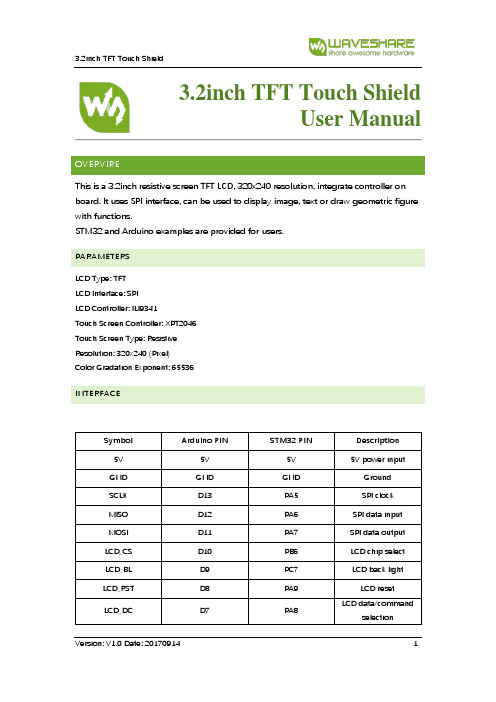
3.2inch TFT Touch ShieldUser ManualOVERVIREThis is a 3.2inch resistive screen TFT LCD, 320x240 resolution, integrate controller on board. It uses SPI interface, can be used to display image, text or draw geometric figure with functions.STM32 and Arduino examples are provided for users.PARAMETERSLCD Type: TFTLCD Interface: SPILCD Controller: ILI9341Touch Screen Controller: XPT2046Touch Screen Type: ResistiveResolution: 320x240 (Pixel)Color Gradation Exponent: 65536INTERFACESymbol Arduino PIN STM32 PIN Description 5V 5V 5V 5V power inputGND GND GND GroundSCLK D13 PA5 SPI clockMISO D12 PA6 SPI data inputMOSI D11 PA7 SPI data outputLCD_CS D10 PB6 LCD chip selectLCD_BL D9 PC7 LCD back lightLCD_RST D8 PA9 LCD resetLCD_DC D7 PA8 LCD data/commandselectionHOW TO USEHARDWARE CONFIGURATION•If there is ICSP interface on Arduino board, set the SPI Config switch to ICSP position.(default)•If Arduino board has no ICSP interface, set the SPI Config switch to the position that SCLK\D13, MISO\D12, MOSI\D11EXAMPLESWe provide Arduino UNO examples and XNUCLEO-F103RB examples for this screen.ARDUINO EXAMPLES1.Download the examples: 3.2inch TFT Touch Shield code.7z, and copy the libraries which arein Arduino\lib folder of examples to the libraries folder which is under the installationdirectory of Arduino.2.Before running the LCD_ShowBMP code, copy the pictures which is in the PIC folder to SDcard.3.Open the LCD_ShowBMP project with Arduino IDE, download to Arduino board.4.The Touch code use four sets of calibration values, could support painting operation in fourdirections. There are five colors which could be chosen on the right. The size of paintbrush is9 by default. Users can also click the AD on screen to calibrate:Please use the stylus click the cross on the screen. The cross will always move until thescreen adjustment is completed.5.According to the prompt, click the red “+” one by one to finish the calibration.STM32 EXAMPLES1.Before running the code that display image. copy the pictures which is in the PIC folder toSD card. Then insert the LCD to NUCLEO or XNUCLEO board.2.Open the project with MDK, download to the NUCLEO or XNUCLEO development board.3.The LCD will first show some general functions: Draw dots, draw dotted line and full line,rectangle, filled rectangle, circle and filled circle. Every figure keeps for 3s. You can change the size of dot, the width of lines and the size of the circles.4.The Touch code use four sets of calibration values, could support painting operation in fourdirections. There are five colors which could be chosen on the right. The size of paintbrush is9 by default. Users can also click the AD on screen to calibrate:Please use the stylus click the cross on the screen. The cross will always move until thescreen adjustment is completed.5.According to the prompt, click the red “+” one by one to finish the calibration.Note:Image: 320x240, 24bit, bmp.SD card: FAT。
TFT彩屏使用说明书
G V N R W R D D D D D D D D R L C N
N C C S R D B B B B B B B B S E S C
D C 0 1 2 3 4 5 6 7 T D
IA
N
| | | | | | | | | | | | | | | | | | | |
CLR_Screen(BLUE);//清屏蓝色
函数名:Put_pixel
功能:在屏幕上画点
函数原型:void Put_pixel(uchar x,uchar y,unsigned int color);
入口参数:x,y 需要画点的坐标,color为点的颜色
出口参数:无
说明:在屏幕上指定的坐标画指定颜色的点
unsigned int forecolor,
unsigned intbkcolor);
入口参数:x 横坐标,y 纵坐标
bColor 字符背景颜色
出口参数:无
说明:需包含"8X16.h",显示数字、大小写英文字符和一些符号等
示例代码:
LCD_PutChar8x16(0,0,'Z',RED,BLUE);//显示英文字符Z
函数名:PutGB1616
功能:显示16*16汉字
函数原型:void PutGB1616
(uR_Screen
功能:清屏
函数原型:void CLR_Screen(unsigned intbColor);
入口参数:bColor清除屏幕的的颜色
出口参数:无
说明:使用背景色清除屏上所有内容
示例代码:
CLR_Screen(0xf800);//清屏红色
TFT彩屏使用说明书..

2.4寸TFT彩屏使用说明书彩屏驱动IC:ILI9325实验板:LY-51S实验板编写:侯瑞阳2013年01月一、彩屏模块简介屏幕尺寸:2.4寸TFT彩屏分辨率:320x240 262K色接口类型:8位数据接口,接口兼容12864液晶接口,①脚对齐电源类型:5V电源接口,板上有3.3V稳压芯片,不需要电平转换SD卡模式:SPI模式触摸IC:XPT2046图1-1 2.4寸TFT彩屏模块二、彩屏结构组成及原理TFT屏(Thin Film Transistor)是薄膜晶体管型液晶显示屏,它的每一个象素点都是由集成在其后的薄膜晶体管来驱动的,这样不仅提高了显示屏的响应速度,同时可以精确控制显示色阶,所以TFT液晶的色彩更逼真。
TFT屏主要的构成包括:背光源、导光板、偏光板、滤光板、玻璃基板、配向膜、液晶材料、薄膜晶体管等。
图2-1 彩屏的基本结构图2-2 TFT彩屏内部结构TFT液晶模块可以显示数字、中英文字符和图案。
彩色,图案分辨率较高。
由于TFT显示器成本日渐降低,并且人们越来越渴望拥有用户友好程度更高的图形界面,因此有越来越多的工程师把TFT显示器设计到他们的产品中去。
TFT模块尺寸指屏幕的对角线长度。
常用有:1.6、1.8、2.0、2.2、2.4 、2.6、2.8、3.0、3.2、3.4、3.6、4、4.3、5.7 、8.4 、10.4 、15 、17 、19 、21 英寸等。
屏幕高宽比小尺寸TFT模块一般是3:4,大尺寸的也有16:9的。
分辨率指水平像素和垂直像素的数量。
三、学习彩屏的准备知识1、什么是图形和图像图形:如一段直线,在单片机内存储时只需要存储起点X、Y坐标和终点X、Y 坐标,存储量极小,但在显示器上显示时,和图像的显示是一致的,也是通过像素点的组合来显示的。
图3-1 像素点组成图形图像:如一张人物照片,在单片机内存储时需要存储所有像素点的信息,存储量极大,在显示器上显示时,通过像素点的点阵组合来完成显示的图3-2 像素点组成图像2、什么是像素像素:图像的最小组成单位。
TFT的基本驱动原理和ASIC的功能介绍

一、主旨:今天主要学习的是TFT的基本驱动原理和ASIC的功能介绍。
二、內容:TFT-LCD的面板构造主要分为背光板、下偏光板、液晶、滤光片、上偏光板组成。
每个液晶面板由一个个液晶单元构成,每个单元由TFT、SOURCE线、GATE线、液晶电容、存储电容构成。
TFT有5道光罩制程, 每道的具体制程为GE(Gate层电极)、SE(Gate层绝缘极、Channel、通道与电极之接触界面)、SD(Source/Drain电极)、CH(Contact hole)、PE(画素电极)。
TFT的基本物理特性⏹温度上升-载子飘移率(ufe)亦上升⏹温度上升-临限电压(Vth)下降⏹照光越強-光漏电流(Iph)越大⏹电压频率越高-闸源与电极电容(Cgd, Cgs)越小⏹a-Si:H的能隙为1.7eV(~800nm)⏹a-Si:H的介电常数为11.7⏹SiNx的介电常数为6.9-7.5(根据N的不同比例)TFT的基本驱动原理TFT元件的动作类似一个开关,液晶元件的作用类似一个电容,借开关的ON/OFF对电容存储的电压值进行更新/保持。
SW ON时信号写入(加入、记录)在液晶电容上,在以外时间SW OFF,可防止信号从液晶电容泄漏。
在必要時可将保持电容与液晶电容并联,以改善其保持特性。
信号传输格式主要有四种●Analog interface(类比讯号)—传统的界面,如CRT。
●Digital interface(数字讯号)—TTL/CMOS,最基本的数字信号,优点:最直接的信号,可直接测量;缺点:易受外界干扰,易向外界干扰,消耗功率大。
●LVDS : Low Voltage Differential Signaling(低压差分信号)— 6bits为4对,8bits为5对,摆幅为250、350、450mV,数据传输速度是7倍的CLK速度,使用这种方式可以减少功率消耗及减低EMI。
●RSDS : Reduced Swing Differential Signaling(低摆幅差分信号)—基于LVDS上,一对Data,RSDS的电压摆幅只有200mV,比LVDS更低,减小电源消耗和辐射,减小计算成分和基板的尺寸。
TFT LCD 指南说明书
Instruction ManualOverviewAn IPS, full colour TFT module, offering 80 degree viewing angles allround, with a 500nit backlight. It is a transmissive type display operating in the normally black mode.This TFT LCD has a 0.96-inch diagonally measured active display area with 80 x 160 dot (80 horizontal by 160 vertical pixel) resolution. Each pixel is divided into Red, Green, Blue dots which are arranged in vertical stripes.Technical Specificationsz Size: 0.96 inchz Dot Matrix: 80 x RGB x 160(TFT) dotsz Module dimension: 30.00(W) x 28.00(H) x 3.00(D) mmz Active area: 10.8 x 21.696 mmz Dot pitch: 0.135 x 0.1356 mmz LCD type: TFT, Normally black, Transmissivez Viewing Angle: 80/80/80/80z Aspect Ratio: 1:2z IC: ST7735Sz Backlight Type: LED,Normally Whitez With /Without TP: Without TPz Surface: Glare*Colour tone slight changed by temperature and driving voltage.InterfaceTechnical DrawingAbsolute Maximum Ratings1. Temp. ≤60˚C, 90% RH MAX. Temp.>60˚C, Absolute humidity shall be less than 90% RH at 60˚C.Electrical CharacteristicsOperating conditions:Note 1 : There are 1 Groups LEDNote 2 : Ta = 25 ˚CNote 3 : Brightness to be decreased to 50% of the initial valueNote 4 : The single LED lamp caseData Colour Coding3-Wire SPI Mode: RGB 5-6-5-bit Input, 65K-Colours, 3AH=“05h”Look-up table for 65k colour mapping (16 bits to 18 bits) Note 1: Pixel data with the 16-bit colour depth informationNote 2: The most significant bits are: Rx4, Gx5 and Bx4Note 3: The least significant bits are: Rx0, Gx0 and Bx04-Wire SPI Mode: RGB 5-6-5-bit Input, 65K-Colours, 3AH=“05h”Look-up table for 65k colour mapping (16 bits to 18 bits) Note 1. Pixel data with the 16-bit colour depth informationNote 2. The most significant bits are: Rx4, Gx5 and Bx4Note 3. The least significant bits are: Rx0, Gx0 and Bx0Display Options availableDisplay on pcb no mountingTFT display as a stand-alone itemOptical CharacteristicsTa=25±2˚CNote 1: Definition of viewing angle rangeNote 2: Test equipment setup:After stabilizing and leaving the panel alone at a driven temperature for 10 minutes, the measurement should be executed. Measurement should be executed in a stable, windless, and dark room. Optical specifications are measured by Topcon BM-7orBM-5 luminance meter 1.0° field of view at a distance of 50cm and normal direction.Note 3: Definition of Response time:The response time is defined as the LCD optical switching time interval between “White” state and “Black” state. Rise time, Tr, is the time between photo detector output intensity changed from 90%to 10%.Black(TFT ON)White(TFT OFF)White(TFT OFF)100%90%10%0%DisplayNote 4: Definition of contrast ratio:The contrast ratio is defined as the following expression.Luminance measured when LCD on the “White” state Contrast ratio (CR) = Luminance measured when LCD on the “Black” stateNote 5: White Vi = Vi50 ± 1.5V Black Vi = Vi50 ± 2.0V“±” means that the analog input signal swings in phase with VCOM signal.“±” means that the analog input signal swings out of phase with VCOM signal.The 100% transmission is defined as the transmission of LCD panel when all the input terminals of module are electrically opened.Note 6: Definition of colour chromaticity (CIE 1931)Colour coordinates measured at the center point of LCDNote 7: Measured at the center area of the panel when all the input terminals of LCD panel are electrically opened.ReliabilityContent of Reliability Test (Wide temperature, -20˚C~70˚C)Environmental TestNote1: No dew condensation to be observed.Note2: The function test shall be conducted after 4 hours storage at the normal Temperature and humidity after remove from the test chamber.Note3: The packing have to including into the vibration testing.。
TFT LCD液晶显示器的驱动原理详解

TFT LCD液晶显示器的驱动原理TFT LCD液晶显示器的驱动原理(一)我们针对TFT LCD的整体系统面来做介绍, 也就是对其驱动原理来做介绍, 而其驱动原理仍然因为一些架构上差异的关系, 而有所不同. 首先我们来介绍由于Cs(storage capacitor)储存电容架构不同, 所形成不同驱动系统架构的原理.Cs(storage capacitor)储存电容的架构一般最常见的储存电容架构有两种, 分别是Cs on gate与Cs on common这两种. 这两种顾名思义就可以知道, 它的主要差别就在于储存电容是利用gate走线或是common走线来完成的. 在上一篇文章中, 我曾提到, 储存电容主要是为了让充好电的电压,能保持到下一次更新画面的时候之用. 所以我们就必须像在CMOS的制程之中, 利用不同层的走线, 来形成平行板电容. 而在TFT LCD的制程之中, 则是利用显示电极与gate走线或是common走线,所形成的平行板电容,来制作出储存电容Cs.图1就是这两种储存电容架构, 从图中我们可以很明显的知道, Cs on gate由于不必像Cs on common一样, 需要增加一条额外的common走线, 所以它的开口率(Aperture ratio)会比较大. 而开口率的大小, 是影响面板的亮度与设计的重要因素. 所以现今面板的设计大多使用Cs on gate的方式. 但是由于Cs on gate的方式, 它的储存电容是由下一条的gate走线与显示电极之间形成的.(请见图2的Cs on gate与Cs on common的等效电路) 而gate走线, 顾名思义就是接到每一个TFT的gate端的走线, 主要就是作为gate driver送出信号, 来打开TFT, 好让TFT对显示电极作充放电的动作. 所以当下一条gate走线, 送出电压要打开下一个TFT时 ,便会影响到储存电容上储存电压的大小. 不过由于下一条gate走线打开到关闭的时间很短,(以1024*768分辨率, 60Hz更新频率的面板来说. 一条gate走线打开的时间约为20us, 而显示画面更新的时间约为16ms, 所以相对而言, 影响有限.) 所以当下一条gate走线关闭, 回复到原先的电压, 则Cs储存电容的电压, 也会随之恢复到正常. 这也是为什么, 大多数的储存电容设计都是采用Cs on gate 的方式的原因.至于common走线, 我们在这边也需要顺便介绍一下. 从图2中我们可以发现, 不管您采用怎样的储存电容架构, Clc的两端都是分别接到显示电极与common. 既然液晶是充满在上下两片玻璃之间, 而显示电极与TFT都是位在同一片玻璃上, 则common电极很明显的就是位在另一片玻璃之上. 如此一来, 由液晶所形成的平行板电容Clc, 便是由上下两片玻璃的显示电极与common电极所形成. 而位于Cs储存电容上的common电极, 则是另外利用位于与显示电极同一片玻璃上的走线, 这跟Clc上的common电极是不一样的, 只不过它们最后都是接到相同的电压就是了.整块面板的电路架构从图3中我们可以看到整片面板的等效电路, 其中每一个TFT与Clc跟Cs所并联的电容, 代表一个显示的点. 而一个基本的显示单元pixel,则需要三个这样显示的点,分别来代表RGB三原色. 以一个1024*768分辨率的TFT LCD来说, 共需要1024*768*3个这样的点组合而成. 整片面板的大致结构就是这样, 然后再藉由如图3中 gate driver所送出的波形, 依序将每一行的TFT打开, 好让整排的source driver同时将一整行的显示点, 充电到各自所需的电压, 显示不同的灰阶. 当这一行充好电时, gate driver便将电压关闭, 然后下一行的gate driver便将电压打开, 再由相同的一排source driver对下一行的显示点进行充放电. 如此依序下去, 当充好了最后一行的显示点, 便又回过来从头从第一行再开始充电. 以一个1024*768 SVGA分辨率的液晶显示器来说, 总共会有768行的g ate走线, 而source走线则共需要1024*3=3072条. 以一般的液晶显示器多为60Hz的更新频率来说, 每一个画面的显示时间约为1/6 0=16.67ms. 由于画面的组成为768行的gate走线, 所以分配给每一条gate走线的开关时间约为16.67ms/768=21.7us. 所以在图3 g ate driver送出的波形中, 我们就可以看到, 这些波形为一个接着一个宽度为21.7us的脉波, 依序打开每一行的TFT. 而sourcedriver则在这21.7us的时间内, 经由source走线, 将显示电极充放电到所需的电压, 好显示出相对应的灰阶.面板的各种极性变换方式由于液晶分子还有一种特性,就是不能够一直固定在某一个电压不变, 不然时间久了, 你即使将电压取消掉, 液晶分子会因为特性的破坏, 而无法再因应电场的变化来转动, 以形成不同的灰阶. 所以每隔一段时间, 就必须将电压恢复原状, 以避免液晶分子的特性遭到破坏. 但是如果画面一直不动, 也就是说画面一直显示同一个灰阶的时候怎么办? 所以液晶显示器内的显示电压就分成了两种极性, 一个是正极性, 而另一个是负极性. 当显示电极的电压高于common电极电压时, 就称之为正极性. 而当显示电极的电压低于c ommon电极的电压时, 就称之为负极性. 不管是正极性或是负极性, 都会有一组相同亮度的灰阶. 所以当上下两层玻璃的压差绝对值是固定时, 不管是显示电极的电压高, 或是common电极的电压高, 所表现出来的灰阶是一模一样的. 不过这两种情况下, 液晶分子的转向却是完全相反, 也就可以避免掉上述当液晶分子转向一直固定在一个方向时, 所造成的特性破坏. 也就是说, 当显示画面一直不动时, 我们仍然可以藉由正负极性不停的交替, 达到显示画面不动, 同时液晶分子不被破坏掉特性的结果. 所以当您所看到的液晶显示器画面虽然静止不动, 其实里面的电压正在不停的作更换, 而其中的液晶分子正不停的一次往这边转, 另一次往反方向转呢!图4就是面板各种不同极性的变换方式, 虽然有这么多种的转换方式, 它们有一个共通点, 都是在下一次更换画面数据的时候来改变极性. 以60Hz的更新频率来说, 也就是每16ms, 更改一次画面的极性. 也就是说, 对于同一点而言, 它的极性是不停的变换的. 而相邻的点是否拥有相同的极性, 那可就依照不同的极性转换方式来决定了. 首先是frame inversion, 它整个画面所有相邻的点, 都是拥有相同的极性. 而row inversion与column inversion则各自在相邻的行与列上拥有相同的极性. 另外在dot inversion上, 则是每个点与自己相邻的上下左右四个点, 是不一样的极性. 最后是delta inversion, 由于它的排列比较不一样, 所以它是以RGB 三个点所形成的pixel作为一个基本单位, 当以pixel为单位时, 它就与dot inversion很相似了, 也就是每个pixel与自己上下左右相邻的pixel,是使用不同的极性来显示的.Common电极的驱动方式图5及图6为两种不同的Common电极的电压驱动方式, 图5中Common电极的电压是一直固定不动的, 而显示电极的电压却是依照其灰阶的不同, 不停的上下变动. 图5中是256灰阶的显示电极波形变化, 以V0这个灰阶而言, 如果您要在面板上一直显示V0这个灰阶的话, 则显示电极的电压就必须一次很高, 但是另一次却很低的这种方式来变化. 为什么要这么复杂呢? 就如同我们前面所提到的原因一样, 就是为了让液晶分子不会一直保持在同一个转向, 而导致物理特性的永久破坏. 因此在不同的frame中, 以V0这个灰阶来说, 它的显示电极与common电极的压差绝对值是固定的, 所以它的灰阶也一直不曾更动. 只不过位在Clc两端的电压, 一次是正的, 称之为正极性, 而另一次是负的, 称之为负极性. 而为了达到极性不停变换这个目的, 我们也可以让common电压不停的变动, 同样也可以达到让Clc两端的压差绝对值固定不变, 而灰阶也不会变化的效果, 而这种方法, 就是图6所显示的波形变化. 这个方法只是将common电压 一次很大, 一次很小的变化. 当然啦, 它一定要比灰阶中最大的电压还大, 而电压小的时候则要比灰阶中最小的电压还要小才行. 而各灰阶的电压与图5中的一样, 仍然要一次大一次小的变化.这两种不同的Common驱动方式影响最大的就是source driver的使用. 以图7中的不同Common电压驱动方式的穿透率来说, 我们可以看到, 当common电极的电压是固定不变的时候, 显示电极的最高电压, 需要到达common电极电压的两倍以上. 而显示电极电压的提供, 则是来自于source driver. 以图七中common电极电压若是固定于5伏特的话, 则source driver所能提供的工作电压范围就要到10伏特以上. 但是如果common电极的电压是变动的话, 假使common电极电压最大为5伏特, 则source driver的最大工作电压也只要为5伏特就可以了. 就source driver的设计制造来说, 需要越高电压的工作范围, 制程与电路的复杂度相对会提高, 成本也会因此而加高.面板极性变换与common电极驱动方式的选用并不是所有的面板极性转换方式都可以搭配上述两种common电极的驱动方式. 当common电极电压固定不变时, 可以使用所有的面板极性转换. 但是如果common电压是变动的话, 则面板极性转换就只能选用frame inversion与row inversion.(请见表1) 也就是说, 如果你想使用column inversion或是dot inversion的话, 你就只能选用 common电极电压固定不动的驱动方式. 为什么呢? 之前我们曾经提到 common电极是位于跟显示电极不同的玻璃上, 在实际的制作上时, 其实这一整片玻璃都是common电极. 也就是说, 在面板上所有的显示点, 它们的common电压是全部接在一起的. 其次由于gate driver的操作方式是将同一行的所有TFT打开,好让source driver去充电, 而这一行的所有显示点, 它的common电极都是接在一起的, 所以如果你是选用common电极电压是可变动的方式的话, 是无法在一行TFT上, 来同时做到显示正极性与负极性的. 而column inversion与dot inversion的极性变换方式, 在一行的显示点上, 是要求每个相邻的点拥有不同的正负极性的. 这也就是为什么 common电极电压变动的方式仅能适用于frame inv ersion与row inversion的缘故. 而common电极电压固定的方式, 就没有这些限制. 因为其common电压一直固定, 只要source dri ver能将电压充到比common大就可以得到正极性, 比common电压小就可以得到负极性, 所以common电极电压固定的方式, 可以适用于各种面板极性的变换方式.表1面板极性变换方式 可使用的common电极驱动方式Frame inversion固定与变动Row inversion固定与变动Column inversion只能使用固定的common电极电压Dot inversion只能使用固定的common电极电压各种面板极性变换的比较现在常见使用在个人计算机上的液晶显示器, 所使用的面板极性变换方式, 大部分都是dot inversion. 为什么呢? 原因无它, 只因为dot inversion的显示品质相对于其它的面板极性变换方式, 要来的好太多了. 表2是各种面板极性变换方式的比较表. 所谓F licker的现象, 就是当你看液晶显示器的画面上时, 你会感觉到画面会有闪烁的感觉. 它并不是故意让显示画面一亮一灭来做出闪烁的视觉效果, 而是因为显示的画面灰阶在每次更新画面时, 会有些微的变动, 让人眼感受到画面在闪烁. 这种情况最容易发生在使用frame inversion的极性变换方式, 因为frame inversion整个画面都是同一极性, 当这次画面是正极性时, 下次整个画面就都变成了是负极性. 假若你是使用common电压固定的方式来驱动, 而common电压又有了一点误差(请见图8),这时候正负极性的同一灰阶电压便会有差别, 当然灰阶的感觉也就不一样. 在不停切换画面的情况下, 由于正负极性画面交替出现,你就会感觉到Flicker的存在. 而其它面板的极性变换方式, 虽然也会有此flicker的现象, 但由于它不像frame inversion 是同时整个画面一齐变换极性, 只有一行或是一列, 甚至于是一个点变化极性而已. 以人眼的感觉来说, 就会比较不明显. 至于crosstalk 的现象, 它指的就是相邻的点之间, 要显示的资料会影响到对方, 以致于显示的画面会有不正确的状况. 虽然crosstalk的现象成因有很多种, 只要相邻点的极性不一样, 便可以减低此一现象的发生. 综合这些特性, 我们就可以知道, 为何大多数人都使用dot inve rsion了. 表2面板极性变换方式 Flicker的现象 Crosstalk的现象Frame inversion明显 垂直与水平方向都易发生Row inversion不明显 水平方向容易发生Column inversion不明显 垂直方向容易发生Dot inversion几乎没有 不易发生面板极性变换方式, 对于耗电也有不同的影响. 不过它在耗电上需要考量其搭配的common电极驱动方式. 一般来说 common电极电压若是固定, 其驱动common电极的耗电会比较小. 但是由于搭配common电压固定方式的source driver其所需的电压比较高, 反而在source driver的耗电会比较大. 但是如果使用相同的common电极驱动方式, 在source driver的耗电来说,就要考量其输出电压的变动频率与变动电压大小. 一般来说, 在此种情形下, source driver的耗电,会有 dot inversion > row inversion > column inversion > frame inversion的状况. 不过现今由于dot inversion的source driver多是使用PN型的OP, 而不是像row inversi on是使用rail to rail OP, 在source driver中OP的耗电就会比较小. 也就是说由于source driver在结构及电路上的改进, 虽然先天上它的输出电压变动频率最高也最大(变动电压最大接近10伏特,而row inversion面板由于多是使用common电极电压变动的方式,其source driver的变动电压最大只有5伏特,耗电上会比较小), 但dot inversion面板的整体耗电已经减低很多了. 这也就是为什么大多数的液晶显示器都是使用dot inversion的方式.TFT LCD液晶显示器的驱动原理(二)上次跟大家介绍液晶显示器的驱动原理中有关储存电容架构,面板极性变换方式,以及common电压的驱动方式.这次我们延续上次的内容,继续针对feed through电压,以及二阶驱动的原理来做介绍.简单来说Feed through电压主要是由于面板上的寄生电容而产生的,而所谓三阶驱动的原理就是为了解决此一问题而发展出来的解决方式,不过我们这次只介绍二阶驱动,至于三阶驱动甚至是四阶驱动则留到下一次再介绍.在介绍feed through电压之前,我们先解释驱动系统中gate driver 所送出波形的timing图.SVGA分辨率的二阶驱动波形我们常见的1024*768分辨率的屏幕,就是我们通常称之为SVGA分辨率的屏幕.它的组成顾名思义就是以1024*768=7864 32个pixel来组成一个画面的数据.以液晶显示器来说,共需要1024*768*3个点(乘3是因为一个pixel需要蓝色,绿色,红色三个点来组成.)来显示一个画面.通常在面板的规划,把一个平面分成X-Y轴来说,在X轴上会有1024*3=3072列.这3072列就由8颗384输出channel的source driver来负责推动.而在Y轴上,会有768行.这768行,就由3颗256输出channel 的gate driver来负责驱动.图1就是SVGA分辨率的gate driver输出波形的timing图.图中gate 1 ~ 768分别代表着76 8个gate driver的输出.以SVGA的分辨率,60Hz的画面更新频率来计算,一个frame的周期约为16.67 ms.对gate 1来说,它的启动时间周期一样为16.67ms.而在这16.67 ms之间,分别需要让gate 1 ~ 768共768条输出线,依序打开再关闭.所以分配到每条线打开的时间仅有16.67ms/768=21.7us而已.所以每一条gate driver打开的时间相对于整个frame是很短的,而在这短短的打开时间之内,source driver再将相对应的显示电极充电到所需的电压.而所谓的二阶驱动就是指gate driver的输出电压仅有两种数值,一为打开电压,一为关闭电压.而对于common电压不变的驱动方式,不管何时何地,电压都是固定不动的.但是对于common电压变动的驱动方式,在每一个frame开始的第一条gate 1打开之前,就必须把电压改变一次.为什么要将这些输出电压的timing介绍过一次呢?因为我们接下来要讨论的feed thr ough电压,它的成因主要是因为面板上其它电压的变化,经由寄生电容或是储存电容,影响到显示电极电压的正确性.在LCD 面板上主要的电压变化来源有3个,分别是gate driver电压变化,source driver电压变化,以及common电压变化.而这其中影响最大的就是gate driver电压变化(经由Cgd或是Cs),以及common电压变化(经由Clc或是Cs+Clc).Cs on common架构且common电压固定不动的feed through电压我们刚才提到,造成有feed through电压的主因有两个.而在common电压固定不动的架构下,造成feed through电压的主因就只有gate driver的电压变化了.在图2中,就是显示电极电压因为feed through电压影响,而造成电压变化的波形图.在图中,请注意到gate driver打开的时间,相对于每个frame的时间比例是不正确的.在此我们是为了能仔细解释每个f rame的动作,所以将gate driver打开的时间画的比较大.请记住,正确的gate driver打开时间是如同图1所示,需要在一个frame的时间内,依序将768个gate driver走线打开的.所以每个gate走线打开的时间,相对于一个frame的时间,是很短的.当gate走线打开或关闭的那一瞬间,电压的变化是最激烈的,大约会有30~40伏特,再经由Cgd的寄生电容,影响到显示电极的电压.在图3中,我们可以看到Cgd寄生电容的存在位置.其实Cgd的发生,跟一般的CMOS电路一样,是位于MOS的gate 与drain端的寄生电容.但是由于在TFT LCD面板上gate端是接到gate driver输出的走线,因此一但在gate driver输出走在线的电压有了激烈变化,便会影响到显示电极上的电压.在图2之中,当Frame N的gate走线打开时,会产生一个向上的feed through电压到显示电极之上.不过此时由于gate走线打开的缘故,source driver会对显示电极开始充电,因此即便一开始的电压不对(因为feed through电压的影响),source driver仍会将显示电极充电到正确的电压,影响便不会太大.但是如果当gate走线关闭的时候,由于source driver已经不再对显示电极充电,所以gate driver关闭时的电压压降(30~40伏特),便会经由Cgd寄生电容feed through到显示电极之上,造成显示电极电压有一个feed through的电压压降,而影响到灰阶显示的正确性.而且这个feed through电压不像gate走线打开时的feed through电压一样,只影响一下子,由于此时source driver已经不再对显示电极充放电,feed through电压压降会一值影响显示电极的电压,直到下一次gate driver走在线的电压再打开的时后.所以这个feed through电压对于显示画面的灰阶的影响,人眼是可以明确的感觉到它的存在的.而在Frame N+1的时候,刚开始当gate driver走线打开的那一瞬间,也会对显示电极产生一个向上的feed through电压,不过这时候由于gate已经打开的缘故,source driver会开始对显示电极充电,因此这个向上的feed through电压影响的时间便不会太长.但是当gate走线再度关闭的时候,向下的feed through电压便会让处在负极性的显示电极电压再往下降,而且受到影响的负极性显示电压会一直维持到下一次gate走线再打开的时候.所以整体来说,显示电极上的有效电压,会比source driver的输出电压要低.而减少的电压大小刚好为gate走线电压变化经由Cgd的feed through电压.这个电压有多大呢?在图4中,我们以电荷不灭定律,可以推导出feed through电压为 (Vg2 – Vg1) * Cgd / (Cgd + Clc + Cs) .假设Cg d=0.05pF,而Clc=0.1pF, Cs=0.5pF且gate走线从打开到关闭的电压为 –35伏特的话. 则feed through电压为 –35*0.0 5 / (0.05+0.1+0.5) = 2.69伏特. 一般一个灰阶与另一个灰阶的电压差约仅有30到50 mV而已(这是以6 bit的分辨率而言,若是8 bit分辨率则仅有3到5 mV而已).因此feed through电压影响灰阶是很严重的.以normal white的偏光板配置来说,会造成正极性的灰阶会比原先预期的来得更亮,而负极型的灰阶会比原先预期的来得更暗.不过恰好feed through电压的方向有一致性,所以我们只要将common电压向下调整即可.从图2中我们可以看到,修正后的common电压与原先的comm on电压的压差恰好等于feed through电压.Cs on common架构且common电压变动的feed through电压图5为Cs on common且common电压变动的电压波形,由于其common电压是随着每一个frame而变动的,因此跟common 电压固定的波形比较起来.其产生的feed through电压来源会再多增加一个,那就是common电压的变化.这个common电压的变化,经由Clc+Cs的电容,便会影响到显示电极的电压.且由于整个LCD面板上所有显示点的Clc与Cs都是接到common电压,所以一但common电压有了变化,受影响的就是整个面板的所有点.跟前面gate电压变化不一样的是,gate电压变化影响到的只是一整行的显示点而已.不过Common电压变化虽然对显示电极的电压有影响,但是对于灰阶的影响却没有像gate电压变化来的大.怎么说呢?如果我们使用跟前面一样的电容参数值,再套用图6所推导出来的公式,再假设Common电压由0伏特变到5伏特,则common电压变化所产生的feed through电压为(5 -0)*(0.1pF+ 0.5pF) / (0.05pF + 0.1pF +0.5pF) = 5 * 0.6 /0.65=4.62伏特.虽然显示电极增加这么多电压,但是common电极也增加了5伏特.因此在Clc两端,也就是液晶的两端,所看到的压差变化,就只有4.62-5=0.38伏特而已.跟之前gate走线电压变化所产生的feed through电压2.69伏特比较起来要小的多了,所以对灰阶的影响也小多了.且由于它所产生的feed through电压有对称性,不像Gate走线所产生的feedthrough电压是一律往下,所以就同一个显示点来说,在视觉对灰阶的表现影响会比较小.当然啦,虽然比较小,但是由于对整个LCD面板的横向的768行来说, common电压变化所发生的时间点,跟gate走线打开的时间间隔并不一致,所以对整个画面的灰阶影响是不一样的.这样一来,就很难做调整以便改进画面品质,这也是为什么common电压变动的驱动方式,越来越少人使用的缘故.Cs on gate架构且common电压固定不动的feed through电压图7是Cs on gate且common电压固定不动的电压波形图.它并没有common电压变化所造成的feed through电压,它只有由于gate电压变化所造成的feed through电压.不过它跟Cs on common不一样的是,由gate电压变化所造成的feed th rough电压来源有两个地方,一个是自己这一条gate走线打开经由Cgd产生的feed through电压,另一个则是上一条gate 走线打开时,经由Cs所产生的feed through电压.经由Cgd的feed through电压跟前面所讨论过的状况是一样的,在这边就不再提了.但是经由Cs的feed through电压,是因为Cs on gate的关系,如图3所示.Cs on gate的架构,它的储存电容另一端并不是接到common电压,而是接到前一条gate走线,因此在我们这一条gate走线打开之前,也就是前一条gate走线打开时,在前一条gate走线的电压变化,便会经由Cs对我们的显示电极造成feed through电压.依照图8的公式,同时套用前面的电容参数与gate电压变化值,我们可得到此一feed through电压约为 35*0.5pF/(0.5pF+0.1pF+0.05pF)=26.92伏特.这样的feed through电压是很大的,不过当前一条gate走线关闭时,这个feed through电压也会随之消失.而且前一条gat e走线从打开到关闭,以SVGA分辨率的屏幕来说,约只有21.7us的时间而已.相对于一个frame的时间16.67ms是很短的.再者当前一条gate走线的feed through电压影响显示电极后,我们这一条的gate走线也随之打开,source driver立刻将显示电极的电压充放电到所要的目标值.从这种种的结果看来,前一条gate走线的电压变化,对于我们的显示电极所表现的灰阶,几乎是没有影响的.因此对于Cs on gate且common电压固定不动的驱动方式来说,影响最大的仍然是gate走在线电压变化经由Cgd产生的feed through电压,而其解决方式跟前面几个一样,只需将common电压往下调整即可.Cs on gate架构且common电压变动的feed through电压图9是Cs on gate架构且common电压变动的feed through电压波形图.这样子的架构,刚好有了前面3种架构的所有缺点,那就是 gate走线经由Cgd的feed through电压,和前一条gate走线经由Cs的feed through电压,以及Common电压变化经由Clc的feed through电压.可想而知,在实际的面板设计上几乎是没有人使用这种架构的.而这4种架构中最常用的就是 Cs on gate架构且common电压固定不动的架构.因为它只需要考虑经由Cgd的feed through电压,而Cs on gate的架构可得到较大的开口率的缘故.。
新荷 Haven 显示 7.0 英寸 TFT 模块 (SPI) - 支持显示、触摸、音频说明书
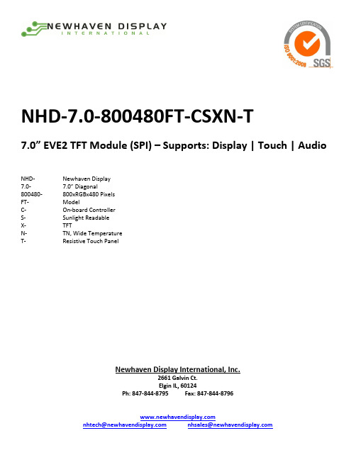
NHD-7.0-800480FT-CSXN-T7.0” EVE2 TFT Module (SPI) – Supports: Display | Touch | Audio NHD- Newhaven Display7.0- 7.0” Diagonal800480- 800xRGBx480 PixelsFT- ModelC- On-board ControllerS- Sunlight ReadableX- TFTN- TN, Wide TemperatureT- Resistive Touch PanelNewhaven Display International, Inc.2661 Galvin Ct.Elgin IL, 60124Ph: 847-844-8795 Fax: 847-844-8796Functions and Features∙7.0” Sunl ight Readable EVE2 TFT Module w/ Resistive Touch∙On-board FTDI/Bridgetek FT812 Embedded Video Engine (EVE2)∙Supports Display, Touch, Audio∙SPI Interface (D-SPI/Q-SPI modes available)∙1MB of Internal Graphics RAM∙Built-in Scalable Fonts∙24-bit True Color, 800x480 Resolution (WVGA)∙Supports Portrait and Landscape modes∙Sunlight Readable (780 cd/m²)∙On-board ON Semiconductor FAN5333BSX High Efficiency LED Driver w/ PWM ∙4x Mounting Holes, enabling standard M3 or #6-32 screws∙Open-Source Hardware, Engineered in Elgin, IL (USA)[read caution below]CN2: FFC Connector - 20-Pin, 1.0mm pitch, Top-contact.NOTICE: It is not recommended to apply power to the board without a display connected. Doing so may result in a damaged LED driver circuit. Newhaven Display does not assume responsibility for failures due to this damage. Controller InformationThis EVE2 TFT Module is powered by the FTDI/Bridgetek FT812 Embedded Video Engine (EVE2).To view the full FT81x specification, please download it by accessing the link below:/Support/Documents/DataSheets/ICs/DS_FT81x.pdfThis product consists of the above TFT display assembled with a PCB which supports all the features of this module. For more details on the TFT display itself, please download the specification at:/specs/NHD-7.0-800480EF-ASXN-T.pdfArduino ApplicationIf using or prototyping this EVE2 TFT Module with the low-cost, widely popular Arduino platform we highly recommend using our Arduino shield, the NHD-FT81x-SHIELD. Not only does the NHD-FT81x-SHIELD provide seamless connectivity and direct software compatibility for the user, but it also comes with the following useful features on-board: ∙logic level shifters to allow the 5V Arduino to communicate with the 3.3V FT81x∙regulators to allow the Arduino to output more current to the EVE2 TFT Module∙audio filter/amplifier circuit to utilize the EVE2 TFT Module’s audio output signal∙microSD card slot, which allows expandable storage for data such as images, video, and audio to be stored. Please visit the NHD-FT81x-SHIELD product webpage for more info.Backlight Driver ConfigurationThe Backlight Driver Enable signal is connected to the FT81x backlight control pin. This signal is controlled by two registers: REG_PWM_HZ and REG_PWM_DUTY. REG_PWM_HZ specifies the PWM output frequency – the range available on the FT81x is 250 to 10000Hz, however the on-board backlight driver’s ma x PWM frequency is 1000Hz. Therefore, for proper use of the PWM function available on this module, the PWM frequency should not exceed 1000Hz. REG_PWM_DUTY specifies the duty cycle – the range is 0 to 128. A value of 0 turns the backlight completely off, while a value of 128 provides maximum backlight brightness.For the above register definitions, please refer to pages 80-81 of the official FT81x Series Programmers Guide:/Support/Documents/ProgramGuides/FT81X_Series_Programmer_Guide.pdfFT81x Block DiagramFT81x with EVE (Embedded Video Engine) technology simplifies the system architecture for advanced Human Machine Interfaces (HMIs) by providing support for display, touch, and audio as well as an object oriented architecture approach that extends from display creation to the rendering of the graphics.Serial Host InterfaceBy default the SPI slave operates in the SINGLE channel mode with MOSI as input from the master and MISO as output to the master. DUAL and QUAD channel modes can be configured through the SPI slave itself. To change the channel modes, write to register REG_SPI_WIDTH. Please refer to the table below:For more details on the FT81x SPI interface, please refer to pages 13-15 of the official FT81x Datasheet:/Support/Documents/DataSheets/ICs/DS_FT81x.pdfFor the REG_SPI_WIDTH register definition, please refer to page 87 of the official FT81x Series Programmers Guide: /Support/Documents/ProgramGuides/FT81X_Series_Programmer_Guide.pdfTFT Timing CharacteristicsShown below are the FT81x registers that control the TFT’s timing (clock and sync signals), along with the values recommended to use for this EVE2 TFT Module:Graphics EngineThe graphics engine executes the display list once for every horizontal line. It executes the primitive objects in the display list and constructs the display line buffer. The horizontal pixel content in the line buffer is updated if the object is visible at the horizontal line.Main features of the graphics engine are:∙The primitive objects supported by the graphics processor are: lines, points, rectangles, bitmaps (comprehensive set of formats), text display, plotting bar graph, edge strips, and line strips, etc.∙Operations such as stencil test, alpha blending and masking are useful for creating a rich set of effects such as shadows, transitions, reveals, fades and wipes.∙Anti-aliasing of the primitive objects (except bitmaps) gives a smoothing effect to the viewer.∙Bitmap transformations enable operations such as translate, scale and rotate.∙Display pixels are plotted with 1/16th pixel precision.∙Four levels of graphics states∙Tag buffer detectionThe graphics engine also supports customized built-in widgets and functionalities such as jpeg decode, screen saver, calibration etc. The graphics engine interprets commands from the MPU host via a 4 Kbyte FIFO in the FT81x memory at RAM_CMD. The MPU/MCU writes commands into the FIFO, and the graphics engine reads and executes the commands. The MPU/MCU updates the register REG_CMD_WRITE to indicate that there are new commands in the FIFO, and the graphics engine updates REG_CMD_READ after commands have been executed.Main features supported are:∙Drawing of widgets such as buttons, clock, keys, gauges, text displays, progress bars, sliders, toggle switches, dials, gradients, etc.∙JPEG and motion-JPEG decode∙Inflate functionality (zlib inflate is supported)∙Timed interrupt (generate an interrupt to the host processor after a specified number of milliseconds)∙In-built animated functionalities such as displaying logo, calibration, spinner, screen saver and sketch∙Snapshot feature to capture the current graphics displayFor a complete list of graphics engine display commands and widgets, please refer to Chapter 4 of the officialFT81x Series Programmers Guide:/Support/Documents/ProgramGuides/FT81X_Series_Programmer_Guide.pdfTouch-Screen EngineThe resistive touch-screen consists of a Touch-Screen Engine, ADC, Axis-switches, and ADC input multiplexer.The Touch-Screen Engine reads commands from the memory map register and generates the required control signals to the axis-switches and inputs mux and ADC. The ADC data are acquired, processed and updated in the respective register for the MPU/MCU to read.For more details on the FT812 Touch-Screen Engine, please refer to pages 32-33 of the official FT81x Datasheet:/Support/Documents/DataSheets/ICs/DS_FT81x.pdfAudio EngineThe FT81x provides mono audio output through a PWM output pin, AUDIO_L. It outputs two audio sources, the sound synthesizer and audio file playback.This pin is designed to be passed into a simple filter circuit and then passed to an amplifier for best results. Please refer to the example schematic in the Audio Filter and Amplifier Reference Circuit section on the next page.Sound SynthesizerA sound processor, AUDIO ENGINE, generates the sound effects from a small ROM library of waves table. To play a sound effect listed in Table 4.3, load the REG_SOUND register with a code value and write 1 to the REG_PLAY register. The REG_PLAY register reads 1 while the effect is playing and returns a ‘0’ when the effect ends. Some sound effects play continuously until interrupted or instructed to play the next sound effect. To interrupt an effect, write a new value to REG_SOUND and REG_PLAY registers; e.g. write 0 (Silence) to REG_SOUND and 1 to PEG_PLAY to stop the sound effect.The sound volume is controlled by register REG_VOL_SOUND. The 16-bit REG_SOUND register takes an 8-bit sound in the low byte. For some sounds, marked "pitch adjust" in the table below, the high 8 bits contain a MIDI note value. For these sounds, a note value of zero indicates middle C. For other sounds the high byte of REG_SOUND is ignored. Audio PlaybackThe FT81x can play back recorded sound through its audio output. To do this, load the original sound data into theFT81x’s RAM, and set r egisters to start the playback. The registers controlling audio playback are:REG_PLAYBACK_START: The start address of the audio data.REG_PLAYBACK_LENGTH: The length of the audio data, in bytes.REG_PLAYBACK_FREQ: The playback sampling frequency, in Hz.REG_PLAYBACK_FORMAT: The playback format, one of LINEAR SAMPLES, uLAW SAMPLES, orADPCM SAMPLES.REG_PLAYBACK_LOOP: If ‘0’, the sample is played once. If ‘1’, the sample is repeated indefinitely.REG_PLAYBACK_PLAY: A write to this location triggers the start of audio playback, regardless ofwriting ‘0’ or ‘1’. Read back ‘1’ when playback is ongoing, and ‘0’ wh enplayback finishes.REG_VOL_PB: Playback volume, 0-255.The mono audio formats supported are 8-bits PCM, 8-bits uLAW and 4-bits IMA-ADPCM. For ADPCM_SAMPLES, each sample is 4 bits, so two samples are packed per byte, the first sample is in bits 0-3 and the second is in bits 4-7.The current audio playback read pointer can be queried by reading the REG_PLAYBACK_READPTR. Using a large sample buffer, looping, and this read pointer, the host MPU/MCU can supply a continuous stream of audio.For more details on the FT81x Audio Engine, please refer to pages 30-32 of the official FT81x Datasheet:/Support/Documents/DataSheets/ICs/DS_FT81x.pdfAdditional Information/ResourcesFT81x Datasheet:FTDI/Bridgetek FT81x Embedded Video Engine (EVE2)/Support/Documents/DataSheets/ICs/DS_FT81x.pdfProgrammers Guide:FT81x Series Programmers Guide/Support/Documents/ProgramGuides/FT81X_Series_Programmer_Guide.pdfNHD GitHub Page:NHD EVE2 TFT Module Example Projectshttps:///NewhavenDisplay/EVE2-TFT-ModulesEVE2 Software Examples:FT81x Example Projects/Support/SoftwareExamples/FT800_Projects.htmFTDI/Bridgetek Utilities:Screen Designer/Support/Utilities.htm#ESD3Image Converters/Support/Utilities.htm#EVEImageConvertersAudio Converter/Support/Utilities.htm#EVEAudioConverterFont Converter/Support/Utilities.htm#EVEFontConverterFT80x to FT81x Migration Guide:FT80x to FT81x Migration Guide/Support/Documents/AppNotes/AN_390%20FT80x%20To%20FT81x%20Migration%20Guide.pdfNote 2: Conducted after 4 hours of storage at 25⁰C, 0%RH.Note 3:Test performed on product itself, not inside a container.Precautions for using LCDs/LCMsSee Precautions at /specs/precautions.pdfWarranty InformationSee Terms & Conditions at /index.php?main_page=terms。
p-Si TFT-LCD的显示驱动原理及驱动技术

二 、PS F .C 的驱动技 术 -i TL D T
T T L D 驱 动 方 案 有 两 种 : a S T T 动 技 术 和 p S F—C 的 —i F驱 —i T T 动技术 。较 之a S T T 术 ,p S T T F驱 — i F技 — i F 驱动技术 的优 势 所在为:
、
PS F - C 的显示驱 动原理 i T L D T
LD C 的基本 结构 包括 上下 玻璃 基板 、液 晶 、I O 、取 T膜 向膜 、偏 光片 、背 光源 等 。每 一像 素单 元加 入 一个有 源器 件 T T 关 之 后 就 成 为 T T L D F ~ C 玻 璃 基 板 上 配 制 的 F开 F — C 。T T L D 行 扫描 线和列数 据线组 合成 一个个矩 阵 ,T T F 有源器 件和像 素 电极 就 制 作 在 矩 阵 的 交 点 上 。 T T 通 、截 止 接 近 理 想 开 F导 关,此开关控制 了液 晶 电压 的加入 情况 。因此 各个 像素之 间 的寻址完全独立 ,从而消 除了液晶像素之 间的交叉 串扰 ,大 大改善 了图像的对 比度 和清晰度 。图 1 — i F — C 单元 为P s T T L D 像 素 驱 动 电 路 ,V c n 行 扫 描 线 ,V a a 列 数 据 线 ,C C sa 为 dt 为 L 为 液 晶 等 效 电容 ,c 为 存 储 电 容 ,C C S 联 之 后 再 与 开 S L 与C 并 关T T T 1(F )串联 。T 有三 个 电极 :源极 s l 、栅 极G 和漏 极D 。 V cn l s a 与T 的栅极G 连,接入行扫 描信 号;V a a 相 d t 与源极s 相 连 ,接 入列数据信号 ;漏 极D l 出端 。当栅极G 为T 输 为有效 电 平 ( 一般为低 电平 )时,T 导通 ,将列数据信 号电压加到液 1 晶像素上 ,进行显 示。T 截止 时,C C s 存储 的列 数据 1 L 与c 上 信号 电压 能够继续维 持显示,直到下一扫描有效 电平到来 。
晶联讯TFT模块 JLX350-019-BN 使用说明书
JLX350-019-BN使用说明书(焊接式FPC)目 录序号 内 容 标 题 页码1 概述 22 特点 23 外形及接口引脚功能 3~44 基本原理 45 技术参数 4~56 时序特性 5~77 指令功能及硬件接口与编程案例 8~末页1.概述晶联讯电子专注于液晶屏及液晶模块的研发、制造。
所生产JLX350-019型TFT模块由于使用方便、显示清晰,广泛应用于各种人机交流面板。
JLX350-019可以显示320列*480行点阵彩色图片,或显示20个/行*30行16*16点阵的汉字,或显示40个/行*60行8*8点阵的英文、数字、符号。
2.JLX350-019图像型点阵TFT模块的特性2.1结构轻、薄、带背光。
2.2 IC采用ST7796S,功能强大,稳定性好2.3 显示内容:●320*480点阵彩色图片;●可选用32*32点阵或其他点阵的图片来自编汉字,按照32*32点阵汉字来计算可显示10个字/行*15行。
●可选用16*16点阵或其他点阵的图片来自编汉字,按照16*16点阵汉字来计算可显示20个字/行*30行。
2.4指令功能强:例如可以用指令控制显示内容顺时针旋转90、逆时针旋转90°或倒立竖放。
2.5接口方式:并口 或串行接口方式。
2.6工作温度宽:-20℃ - +70℃;2.7工作温度宽:-30℃ - +80℃;3.外形尺寸及接口引脚功能模块的接口引脚功能引 线 号 符 号 名 称 功 能1 GND 接地 0V2 VDD 供电电源正极 供电电源正极3.3V3 CS 片选 低电平片选4 RS 寄存器选择信号 H:数据寄存器 0:指令寄存器5 WR/SCL 写/串行时钟并口:写功能; 串口:串行时钟6 RD 读 并口:读功能,串口:建议接VDD或VSS7 SDA 串行数据 并口:空串口:做串行数据8 NC NC 空脚9 DB0 I/O 并口:数据总线DB0,串口:建议接VDD或VSS10 DB1 I/O 并口:数据总线DB1,串口:建议接VDD或VSS11 DB2 I/O 并口:数据总线DB2,串口:建议接VDD或VSS12 DB3 I/O 并口:数据总线DB3,串口:建议接VDD或VSS13 DB4 I/O 并口:数据总线DB4,串口:建议接VDD或VSS14 DB5 I/O 并口:数据总线DB5,串口:建议接VDD或VSS15 DB6 I/O 并口:数据总线DB6,串口:建议接VDD或VSS16 DB7 I/O 并口:数据总线DB7,串口:建议接VDD或VSS17 RST 复位 低电平复位,复位完成后,回到高电平,TFT模块开始工作18 IM2/PS 接口方式选择 并口:VSS 串口:VDD19 LEDA 背光电源正极 接3.0V(接3.3V串10欧电阻,接5.0V串39欧电阻)20 LEDK 背光电源负极 接GND表1:模块的接口引脚功能4.基本原理4.1TFT屏(LCD)在LCD上排列着320×480点阵,320个列信号与驱动IC相连,480个行信号也与驱动IC相连,IC邦定在LCD玻璃上(这种加工工艺叫COG).4.2背光参数该型号TFT模块带LED 背光源。
1.44寸tftlcd驱动程序详解

1.44寸tftlcd驱动程序详解1.44寸TFT LCD(TFT液晶显示屏)是一种小型彩色液晶屏,通常应用于嵌入式系统和消费电子产品中。
为了使其正常显示图像,需要编写相应的驱动程序。
下面是对1.44寸TFT LCD驱动程序的详细解析:1. 建立通信:首先,需要确定与TFT LCD之间的通信接口,例如SPI (串行外设接口),I2C(串行总线接口)或并行接口等。
根据选定的接口,配置相应的引脚和通信参数,以确保正确的数据传输。
2. 初始化LCD控制器:接下来,需要初始化LCD控制器。
这包括设置控制器的工作模式、像素格式、扫描方向等。
此外,还需设置LCD的分辨率和颜色模式,以确定显示的像素数和色彩深度。
3. 像素数据传输:在驱动程序中,需要实现像素数据的传输和写入。
根据TFT LCD的工作原理,像素数据一般以行为单位进行传输。
通过逐行扫描,将图像数据按照指定的颜色格式和像素排列方式写入LCD的显示缓冲区。
4. 刷新显示:驱动程序需要定期刷新LCD的显示,以确保图像持续显示并且没有残留。
可以使用定时器中断或其他方式来触发刷新操作。
在刷新过程中,将显示缓冲区的数据传输到实际的LCD面板上,使其显示出正确的图像。
5. 特殊功能:根据不同的TFT LCD型号和应用需求,可能还需要实现一些特殊功能。
例如,调节LCD的亮度、对比度和背光等。
这些功能可以通过操作LCD控制器的寄存器来实现。
6. 错误处理:在驱动程序中,还需要添加适当的错误处理机制。
这可以包括检测和处理通信错误、数据传输错误以及其他异常情况。
通过合理的错误处理,可以提高驱动程序的健壮性和可靠性。
综上所述,编写1.44寸TFT LCD驱动程序需要建立通信接口、初始化LCD控制器、像素数据传输、刷新显示、实现特殊功能以及添加错误处理。
这样的驱动程序可以确保TFT LCD正常工作并显示出准确的图像。
驱动程序的编写需要根据具体的硬件规格和驱动芯片的特性进行调整和优化,以实现最佳的性能和用户体验。
SPI480272彩色TFT液晶显示屏面向高性价比的单片机系统、工业控制系统
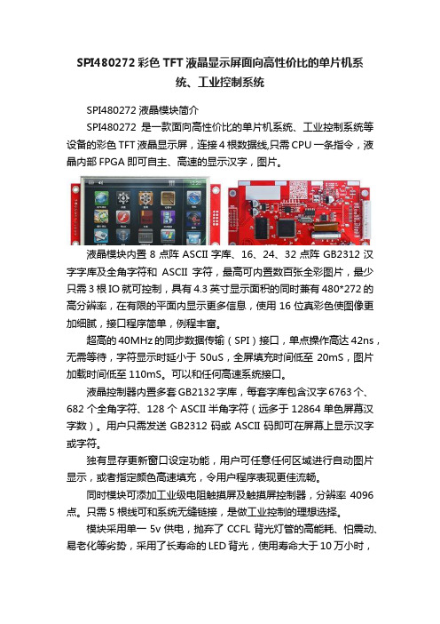
SPI480272彩色TFT液晶显示屏面向高性价比的单片机系统、工业控制系统SPI480272液晶模块简介SPI480272是一款面向高性价比的单片机系统、工业控制系统等设备的彩色TFT液晶显示屏,连接4根数据线,只需CPU一条指令,液晶内部FPGA即可自主、高速的显示汉字,图片。
液晶模块内置8点阵ASCII字库、16、24、32点阵GB2312汉字字库及全角字符和ASCII字符,最高可内置数百张全彩图片,最少只需3根IO就可控制,具有4.3英寸显示面积的同时兼有480*272的高分辨率,在有限的平面内显示更多信息,使用16位真彩色使图像更加细腻,接口程序简单,例程丰富。
超高的40MHz的同步数据传输(SPI)接口,单点操作高达42ns,无需等待,字符显示时延小于50uS,全屏填充时间低至20mS,图片加载时间低至110mS。
可以和任何高速系统接口。
液晶控制器内置多套GB2132字库,每套字库包含汉字6763个、682个全角字符、128个ASCII半角字符(远多于12864单色屏幕汉字数)。
用户只需发送GB2312码或ASCII码即可在屏幕上显示汉字或字符。
独有显存更新窗口设定功能,用户可任意任何区域进行自动图片显示,或者指定颜色高速填充,令用户程序表现更佳流畅。
同时模块可添加工业级电阻触摸屏及触摸屏控制器,分辨率4096点。
只需5根线可和系统无缝链接,是做工业控制的理想选择。
模块采用单一5v供电,抛弃了CCFL背光灯管的高能耗、怕震动、易老化等劣势,采用了长寿命的LED背光,使用寿命大于10万小时,用户不需外加背光条。
颜色纯正,且64级背光亮度软件可调,可降低系统功耗。
一、适用范围:适配CPU:AVR、PIC、STM32系列、LPC2XXX、MSP430、51、DSP、FPGA 96、X86、8088及其他ARM全系列CPU等二、模块特性:三、液晶应用接口1、接口定义:1)LCD接口JP1(XH2.54MM-6P插座,注意此排针位于液晶电路板侧,朝向液晶背侧)2) TOUCH接口JP2(XH2.54MM-5P插座,注意:触摸控制器时钟速率要低于125KHz)3) 综合接口JP3(FPC1.0mm-14P卧贴下接触插座)。
- 1、下载文档前请自行甄别文档内容的完整性,平台不提供额外的编辑、内容补充、找答案等附加服务。
- 2、"仅部分预览"的文档,不可在线预览部分如存在完整性等问题,可反馈申请退款(可完整预览的文档不适用该条件!)。
- 3、如文档侵犯您的权益,请联系客服反馈,我们会尽快为您处理(人工客服工作时间:9:00-18:30)。
北京恒诚昊威科技有限公司
电话:010-62655776 13811689587
TFT LCD 控制模块由 CPLD 产生稳定的 TFT 时序驱动 LCD 面板,以及 SDRAM(显 存)时序读取显存的数据。并能接受 MCU 写入的数据,保存到 SDRAM 的指定位置。
TFT LCD 控制模块 使用说明
一、概述 TFT LCD 控制模块特点: 1、支持 8 位并行 MCU 接口和 SPI 接口。适合一般 51 单片机和 ARM 单片机使用。 2、输入具有双缓冲功能,可获得较高的写入速率和正确的显示效果。 3、16 位并行 RGB 输出接口,可支持 8 位(256 色)显示或 16 位(65K 色)显示。 4、输出时序具有高稳定性,抗干扰能力强。 5、具备 2 页显示页面,切换不闪烁,编程简单。 6、支持 320×240、640×480、800×600 等多种分辨率。 以上不同的特性组合分属不同的具体模块型号。
5)对于 16 位色版本,需要再写入象素颜色数据的高字节,之后控制板才进行保存
动作。
读数据过程和以上类似,但是设置坐标之后,控制板需要时间将显存的数据转移到数据
寄存器,所以根据效果调节写行列号寄存器到读数据寄存器之间的时间间隔,在此 BUSY
信号不起作用。
四、程序样例
以 STC89C516RD+单片机为例,控制板的 A1 接 MCU 的 P2.1,A0 接 MCU 的 P2.0,
void LcdPixel(int x,y,unsigned char color) //640*480 {
LcdOperatPort = (x/256)|((y/64)&0x04); LcdColLowPort = x; LcdRowLowPort = y; LcdDataPort = color; }
指令访问控制板的 4 个寄存器(端口)。具体时序见 8051 手册。 其他处理器,比如带有并行总线但没有 LCD 控制器的 ARM 微控制器,外部总线往往
是 16 位甚至更高,可以只使用其低 8 位,或直接配置为 8 位总线使用。同时,ARM 微控制 器的总线时间参数可以设置,在后面的程序样例中给以说明。
CS 接 MCU 的 P2.7。如此定义以下访问地址的宏:
#define LcdDataPort
*((unsigned char xdata *)0x4000)
#define LcdRowLowPort *((unsigned char xdata *)0x4100)
#define LcdColLowPort *((unsigned char xdata *)0x4200)
北京恒诚昊威科技有限公司
电话:010-62655776 13811689587
BIT15
对应 LCD 信号的 RD5
BIT14
对应 LCD 信号的 RD4
BIT13
对应 LCD 信号的 RD3
BIT12
对应 LCD 信号的 RD2
BIT11
对应 LCD 信号的 RD1
#define LcdOperatPort *((unsigned char xdata *)0x4300)
北京恒诚昊威科技有限公司
电话:010-62655776 13811689587
这里为了避开 STC89C516RD+的内部扩展 RAM 空间,令 P2.6 为 1。 然后编写下面的写入象素的函数,基于此可完成其他画面操作。
对于 8 位色版本的控制模块实际只输出 8 位色,RGB 3-3-2 格式,有效信号是 RD3 到 RD5,RG3 到 RG5 和 RB4、RB5。其余信号均输出低电平。
控制模块上的 R6 和 R5 可以设置 LCD 屏的画面方向,可以水平或垂直翻转画面,具体 参考 LCD 屏的手册。
三、并行接口软件操作说明 1. MCU 接口时序:TFT LCD 控制模块支持标准 8051 系列 MCU 的读写时序,即用 MOVX @DPTR,A MOVX A, @DPTR
4. 对于 8 位色(共 256 种颜色)的控制模块,每操作一个象素读写一个字节的数据即 可。数据字节位定义:
BIT7 红色高 对应 LCD 信号的 RD5 BIT6 红色中 对应 LCD 信号的 RD4 BIT5 红色低 对应 LCD 信号的 RD3 BIT4 绿色高 对应 LCD 信号的 GD5 BIT3 绿色中 对应 LCD 信号的 GD4 BIT2 绿色低 对应 LCD 信号的 GD3 BIT1 蓝色高 对应 LCD 信号的 BD5 BIT0 蓝色低 对应 LCD 信号的 BD4 对于 16 位色(共 65536 种颜色)的控制模块,每操作一个象素需要读写两个字节的 数据,8 位接口则需要分两次传输。先写入低字节,再写入高字节,只有在写入高字节后, 控制板才会认为是一个象素写入,所以软件务必保证写入数据的完整性。 16 位数据高字节位定义:
B0 B1
GND GND
B2
B3
B4
B5
L_BD1 L_BD2 L_BD3 L_BD4 L_BD5
19 20 21 22 23 24 25
GND
L_DEN
26 27
VDD33
28
R5
29
GND
30
0
31
R6
GND
32
GND
LCD
图中 L_CLK、L_HS、L_VS、L_DEN 分别是 LCD 屏的位时钟、水平同步、垂直同步、 数据使能等信号。L_RD1 到 L_RD5 是红色信号,L_GD0 到 L_GD5 是绿色信号,L_BD1 到 L_BD5 是蓝色信号,按 RGB 5-6-5 格式构成 16 位色信号。
BIT2
对应 LCD 信号的 BD3
BIT1
对应 LCD 信号的 BD2
BIT0
对应 LCD 信号的 BD1
5. 由于每次处理器写入数据后,CPLD 都需要时间将显示数据保存到 SDRAM 中的指
定位置,所以控制板有象素写入速度的限制,约 3.75M 次每秒,超过此极限,会出现写入
数据丢失的现象。对于 51 单片机而言,晶体频率 20M,X2 模式,汇编指令连续写入时不
控制模块有一个重要的功能就是,每次写数据寄存器之后,列号(象素的 x 坐标)会自 动加 1,如果软件需要连续写一行内的若干象素,可以连续写数据寄存器,而不用反复设置 列号寄存器。但读数据寄存器时没有 x 坐标自动加 1 功能,一般情况读数据只限于局部,数 据量不大,可以软件反复设置坐标。
控制模块支持双页显示,就是在显存中可保持两个显示页面的数据,软件可以设置其中 一个页面显示在 LCD 屏上,而 MCU 将数据写入另一个页面。显示页面和写入页面相同时 可能会看到数据写入(画面刷新)的过程,而显示页面和写入页面不同时则可避免这个现象, 但一般只适合全屏刷新,比如清屏。
TFT LCD 控制模块在系统中的应用如下图所示:
MCU 用户板
TFT LCD 控制模块
TFT 液晶屏
TFT LCD 控制模块可以通过用户板的薄膜电缆供电。支持 3.3V 的 MCU;驱动 3.3V 的 LCD 屏。
二、TFT LCD 控制模块接口说明。
第1脚 MCU 接口
第1脚 LCD 接口
R6、R5
控制模块引脚位置图
TFT LCD 控制模块和 MCU 系统板的连接插座是 J2 MCUPORT,为 1.0mm 间距 18 脚 的薄膜线插座。引脚定义见下表。
1
GND
2
Data0
3
Data1
4
Data2
5
Data3
6
Data4
7
Data5
8
Data6
9
Data7
10 nRD(SPI_MISO) 11 nWE(SPI_MOSI) 12 A0(SPI_CLK) 13 A1(SPI_C/D) 14 nCS(SPI_CS) 15 GND
2)将 X 坐标的低 8 位写入列号寄存器(A1=1 A0=0)。
3)将 Y 坐标的低 8 位写入行号寄存器(A1=0 A0=1)。
4)将象素颜色数据写入数据寄存器(A1=0 A0=0)。列号寄存器(控制板内部的 x
坐标)会自动加 1。当写入数据寄存器后,控制板才开始进行保存动作,所以必须先行写入
行列地址再写入数据。
2. MCU 信号电平组合:
nCS nWR nRD A1
A0
D0-D7
H
任意 任意 任意 任意 操作无效
L
L
H
0
0
写数据到显存
L
H
L
0
0
从显存读数据
L
L
H
0
1
设置 LCD 行号(垂直 y 坐标)低字节
L
L
H
1
0
设置 LCD 列号(水平 x 坐标)低字节
L
L
H
1
1
设置操作字节(包含行列地址高位)
北京恒诚昊威科技有限公司
16 GND 17 VDD 3.3V 18 VDD 3.3V
当使用 8 位并行接口的模块时,信号线为数据线 Data0-Data7、读控制 nRD、写控制 nWE、地址 A0、A1 和片选 nCS。当使用 SPI 总线接口的模块时,信号线为 SPI_MISO、 SPI_MOSI、SPI_CLK、SPI_C/D(命令/数据)、SPI_CS,此时 Data0-Data1 可接地。
电话:010-62655776 13811689587
3. CPLD 内部含有 4 个寄存器,对 MCU 而言就是 4 个地址端口: 数据寄存器 地址 A1=0 A0=0 MCU 读写显存数据的缓冲寄存器。 行号寄存器 地址 A1=0 A0=1 LCD 行号就是象素的垂直 y 坐标(低 8 位) 列号寄存器 地址 A1=1 A0=0 LCD 列号就是象素的水平 x 坐标(低 8 位) 设置寄存器 地址 A1=1 A0=1 包含行号的高 1 位和列号的高 2 位及其他控制信号