TLC2543采集程序
TLC2543串行AD转换器内部原理

TLC2543串行A/D转换器模块采用TI公司的TLC2543 12位串行A/D转换器,使用开关电容逐次逼近技术完成A/D转换过程。
由于是串行输入结构,能够节省51系列单片机I/O资源,且价格适中。
其特点有:(1)12位分辨率A/D转换器;(2)在工作温度范围内10μs转换时间;(3)11个模拟输入通道;(4)3路内置自测试方式;(5)采样率为66kbps;(6)线性误差+1LSB(max)(7)有转换结束(EOC)输出;(8)具有单、双极性输出;(9)可编程的MSB或LSB前导;(10)可编程的输出数据长度。
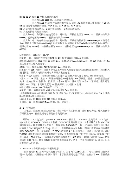
TLC2543的引脚排列如图1所示。
图1中AIN0~AIN10为模拟输入端;为片选端;DIN 为串行数据输入端;DOUT为A/D转换结果的三态串行输出端;EOC为转换结束端;CLK为I/O时钟;REF+为正基准电压端;REF-为负基准电压端;V CC为电源;GND为地TLC2543的使用方法2.1 控制字的格式控制字为从DATAINPUT端串行输入的8位数据,它规定了TLC2543要转换的模拟量通道、转换后的输出数据长度、输出数据的格式。
其中高4位(D7~D4)决定通道号,对于0通道至10通道,该4位分别为0000~1010H,当为1011~1101时,用于对TLC2543的自检,分别测试(V REF++V REF-)/2、V REF-、V REF+的值,当为1110时,TLC2543进入休眠状态。
低4位决定输出数据长度及格式,其中D3、D2决定输出数据长度,01表示输出数据长度为8位,11表示输出数据长度为16位,其他为12位。
D1决定输出数据是高位先送出,还是低位先送出,为0表示高位先送出。
D0决定输出数据是单极性(二进制)还是双极性(2的补码),若为单极性,该位为0,反之为1。
2.2 转换过程上电后,片选CS必须从高到低,才能开始一次工作周期,此时EOC为高,输入数据寄存器被置为0,输出数据寄存器的内容是随机的。
TLC2543程序

//========================================================== ===========// tlc2543驱动程序//tlc2543.c//writer:谷雨2008年3月12日于EDA实验室整理//========================================================== ===========#include#define uint unsigned int#define uchar unsigned char//**************************修改硬件时要修改的部分********************************sbit clock = P0^0; //输入、输出时钟端sbit input = P0^1; //数据输入端sbit output = P0^2; //数据输出端sbit CS = P0^3; //片选端,负电平有效void delay(uchar N){while(N--);}uint read2543(uchar CON_WORD) //CON_WORD为选择的通道,为0--10 {uint ad=0;uchar i;CON_WORD<<=4;clock=0;CS=0;for(i=0;i<12;i++){if(output==1) //读取DATAOUTad=ad|0x01;if(CON_WORD&0x80) //读取控制字到INPUTinput=1;elseinput=0;clock=1;delay(10);clock=0;delay(10);CON_WORD<<=1;ad<<=1;}CS=1;ad>>=1;return(ad);}void init_serial() //初始化串口{TMOD=0x20; //定时器T1使用工作方式2TH1=250; //设置初值TH0=250;TR1=1; //开始计时PCON=0x80; //SMOD=1;SCON=0x50; //工作方式1,波特率9600bit/s,允许接收TI=1;}void main(){uint ad=0;float fVoltage1;uchar buf[5],i;init_serial();IE=0; //屏蔽中断while(1){ad=read2543(0);fVoltage1=(float)ad/0x0fff*5;buf[0]=(uchar)fVoltage1;buf[0]=buf[0]+0x30;buf[1]=''.'buf[2]=(uchar)(fVoltage1*10)%10;buf[2]=buf[2]+0x30;buf[3]=(uchar)(fVoltage1*100-buf[0]*100)%10;buf[3]=buf[3]+0x30;buf[4]=(uchar)((fVoltage1*1000)-buf[0]*1000-buf[1]*100)%10; buf[4]=buf[4]+0x30;i=0;while(i<5){if(TI==1){SBUF=buf[i];TI=0;i++;}}} }。
TLC2543中文资料
D7 D6 D5 D4代表11个模拟通道的地址当其为1100-1110时,选择片内检测电压当其为1111时,为软件选择的断电模式,此时,AD转换器的工作电流只有25uA. D3 D2决定输出数据的长度,01 = 8位;11 = 16位;X1 = 12位D1 决定输出数据的格式,0表示先送高位,1表示先送低位。
D0 决定转换结果输出的格式。
当其为0时,为无极性输出(无符号二进制数),即模拟电压为Vnef+,时,转换的结果为0FFFH;模拟电压为Vnef-时,转换的结果为0000H。
当其为1时,为有极性输出(有符号二进制数),即模拟电压高于(Vnef+-Vnef-)/2时符号位为0;模拟电压低于(Vnef+-Vnef-)/2时符号位为1;模拟电压为Vnef+时,转换的结果为03FFH;模拟电压为Vnef-时,转换的结果为0800H。
模拟电压为(Vnef+-Vnef-)/2时,转换的结果为0000H。
1.初始化时,EOC=“1”,CS=“1”2.使CS下降,前次转换结果的MSB即A11位数据输出到Dout供读数。
3.将输入控制字的MSB位即C7送到Din,在CS之后tsu>=1.425us后,使CLK上升,将Din 上的数据移入输入寄存器。
4.CLK下降,转换结果的A10位输出到Dout供读数。
5.在第4个CLK下降时,由前4个CLK上升沿移入寄存器的四位通道地址被译码,相应模入通道接通,其模入电压开始时对内部开关电容充电。
6.第8个CLK上升时,将Din脚的输入控制字C0位移入输入寄存器后,Din脚即无效。
7.第11个CLK下降,上次AD结果的最低位A0输出到Dout供读数。
至此,I/O数据已全部完成,但为实现12位同步,仍用第12个CLK脉冲,且在其第12个CLK下降时,模入通道断开,EOC下降,本周期设置的AD转换开始,此时使CS上升。
8.经过时间tconv<=10us,转换完毕,EOC上升。
TLC2543

摘要:TLC2543是德州仪器公司生产的12位开关电容型逐次逼近模数转换器,它具有三个控制输入端,采用简单的3线SPI串行接口可方便地与微机进行连接,是12位数据采集系统的最佳选择器件之一。
本文介绍了该芯片的功能、时序,并给出了8051单片机的接口电路。
关键词:模数转换器; SPI串行接口; TLC25431. 概述A/D、D/A转换器是过程及仪器仪表、设备等检测与控制装置中应用比较广泛的器件。
随着大规模集成电路技术的发展,各种高精度、低功耗、可编程、低成本的A/D转换器不断推出,使得微机控制系统的电路更加简洁,可靠性更高。
TLC2543与外围电路的连线简单,三个控制输入端为CS(片选)、输入/输出时钟(I/O CLOCK)以及串行数据输入端(DATA INPUT)。
片内的14通道多路器可以选择11个输入中的任何一个或3个内部自测试电压中的一个,采样-保持是自动的,转换结束,EOC输出变高。
TLC2543的主要特性如下:●11个模拟输入通道;●66ksps的采样速率;●最大转换时间为10μs;●SPI串行接口;●线性度误差最大为±1LSB;●低供电电流(1mA典型值);●掉电模式电流为4μA。
2. TLC2543引脚功能与接口时序2.1 TLC2543引脚排列TLC2543的引脚排列如图1所示。
引脚功能说明如下:AIN0~AIN10:模拟输入端,由内部多路器选择。
对4.1MHz的I/O CLOCK,驱动源阻抗必须小于或等于50Ω;CS:片选端,CS由高到低变化将复位内部计数器,并控制和使能DATA OUT、DATA INPUT 和I/O CLOCK。
CS由低到高的变化将在一个设置时间内禁止DATA INPUT和I/O CLOCK;DATA INPUT:串行数据输入端,串行数据以MSB为前导并在I/O CLOCK的前4个上升沿移入4位地址,用来选择下一个要转换的模拟输入信号或测试电压,之后I/O CLOCK将余下的几位依次输入;DATA OUT:A/D转换结果三态输出端,在CS为高时,该引脚处于高阻状态;当CS为低时,该引脚由前一次转换结果的MSB值置成相应的逻辑电平;EOC:转换结束端。
TLC2543芯片手册_时序_转换原理

A I N 2A I N 1 A I N 0 V C C E O CA I N 8 G N D A I N 9 A I N 10 R E F –Programmable MSB or LSB First Programmable Power DownProgrammable Output Data Length CMOS TechnologyApplication Report Available †FN PACKAGE (TOP VIEW)descriptionThe TLC2543C and TLC2543I are 12-bit, switched- capacitor, successive-approximation, analog-to- digital converters. Each device, with three control inputs [chip select (CS), the input-output clock, and AIN3 AIN4 AIN5 AIN6 AIN74 5 6 7 83 2 1 20 19 1817 16 15 149 10 11 12 13I/O CLOCK DATA INPUT DATA OUT CS REF +the address input (DATA INPUT)], is designed for communication with the serial port of a host processor or peripheral through a serial 3-state output. The device allows high-speed data transfers from the host.In addition to the high-speed converter and versatile control capability, the device has an on-chip 14-channelmultiplexer that can select any one of 11 inputs or any one of three internal self-test voltages. The sample-and-hold function is automatic. At the end of conversion, the end-of-conversion (EOC) output goes high to indicate that conversion is complete. The converter incorporated in the device features differential high-impedance reference inputs that facilitate ratiometric conversion, scaling, and isolation of analog circuitry from logic and supply noise. A switched-capacitor design allows low-error conversion over the full operating temperature range.The TLC2543C is characterized for operation from T A = 0︒C to 70︒C. The TLC2543I is characterized for operation from T A = – 40︒C to 85︒C. The TLC2543M is characterized for operation from T A = – 55︒C to 125︒C.Please be aware that an important notice concerning availability, standard warranty, and use in critical applications of Texas Instruments semiconductor products and disclaimers thereto appears at the end of this data sheet.Based Data Acquisition Using the TLC2543 12-bit Serial-Out ADC (SLAA012)PRODUCTION DATA information is current as of publication date. Products conform to specifications per the terms of Texas Instrumentsstandard warranty. Production processing does not necessarily includetesting of all parameters.Copyright ⎡ 2001, Texas Instruments IncorporatedOn products compliant to MIL-PRF-38535, all parameters are tested unless otherwise noted. On all other products, productionprocessing does not necessarily include testing of all parameters.POST OFFICE BOX 655303∙DALLAS, TEXAS 752651TLC2543C, TLC2543I, TLC2543M12-BIT ANALOG-TO-DIGITAL CONVERTERSWITH SERIAL CONTROL AND 11 ANALOG INPUTSSLAS079F – DECEMBER 1993 – REVISED NOVEMBER 2001AVAILABLE OPTIONSTLC2543IFNR.functional block diagramREF + REF – 1413AIN0 AIN1 AIN2 AIN3 AIN4 AIN5 AIN6 AIN7 AIN8 AIN9 AIN101 2 3 4 5 6 7 8 9 11 1214-Channel Analog Multiplexer4Sample-and- Hold FunctionInput Address Register12-Bit Analog-to-Digital Converter (Switched Capacitors)12Output 12 Data Register12-to-1 Data Selector and Driver 16DATA OUT43Control Logic Self-Test Referenceand I/O CountersDATA17 19 EOCINPUTI/O CLOCKCS18 152POST OFFICE BOX 655303∙DALLAS, TEXAS 75265TAPACKAGE SMALL OUTLINE †† (DB) (DW)PLASTIC CHIPCARRIER † (FN) CERAMIC DIP(J) PLASTIC DIP(N) 0︒C to 70︒C TLC2543CDB TLC2543CDW TLC2543CFN — TLC2543CN –40︒C to 85︒C TLC2543IDB TLC2543IDWTLC2543IFN— TLC2543IN–55︒C to 125︒C— ——TLC2543MJ—TLC2543C,TLC2543I,TLC2543M12-BIT ANALOG-TO-DIGITAL CONVERTERS WITH SERIAL CONTROL AND11ANALOG INPUTSSLAS079F–DECEMBER1993–REVISED NOVEMBER2001 Terminal FunctionsPOST OFFICE BOX655303∙DALLAS,TEXAS752653TLC2543C,TLC2543I,TLC2543M12-BIT ANALOG-TO-DIGITAL CONVERTERSWITH SERIAL CONTROL AND11ANALOG INPUTSSLAS079F–DECEMBER1993–REVISED NOVEMBER2001absolute maximum ratings over operating free-air temperature range(unless otherwise noted)†Supply voltage range,V CC(see Note1).............................................–0.5V to6.5V Input voltage range,V I(any input)............................................–0.3V to V CC+0.3V Output voltage range,V O...................................................–0.3V to V CC+0.3V Positive reference voltage,V ref+......................................................V CC+0.1V Negative reference voltage,V ref–..........................................................–0.1V Peak input current,I I(any input)..........................................................±20mA Peak total input current,I I(all inputs)......................................................±30mA Operating free-air temperature range,T A:TLC2543C...................................0︒C to70︒CTLC2543I.................................–40︒C to85︒CTLC2543M...............................–55︒C to125︒C Storage temperature range,T stg...................................................–65︒C to150︒C Lead temperature1,6mm(1/16inch)from the case for10seconds............................260︒C †Stresses beyond those listed under“absolute maximum ratings”may cause permanent damage to the device.These are stress ratings only,and functional operation of the device at these or any other conditions beyond those indicated under“recommended operating conditions”is not implied.Exposure to absolute-maximum-rated conditions for extended periods may affect device reliability.NOTE1:All voltage values are with respect to the GND terminal with REF–and GND wired together(unless otherwise noted). recommended operating conditionsto REF–convert as all zeros(000000000000).3.To minimize errors caused by noise at the CS input,the internal circuitry waits for a setup time after CS before responding to controlinput signals.No attempt should be made to clock in an address until the minimum CS setup time has elapsed.4.This is the time required for the clock input signal to fall from VIHmin to VILmax or to rise from VILmax to VIHmin.In the vicinity ofnormal room temperature,the devices function with input clock transition time as slow as1∝s for remote data acquisition applicationswhere the sensor and the A/D converter are placed several feet away from the controlling microprocessor.4POST OFFICE BOX655303∙DALLAS,TEXAS75265TLC2543C, TLC2543I, TLC2543M12-BIT ANALOG-TO-DIGITAL CONVERTERSWITH SERIAL CONTROL AND 11 ANALOG INPUTSSLAS079F – DECEMBER 1993 – REVISED NOVEMBER 2001electrical characteristics over recommended operating free-air temperature range, V CC = V ref+ = 4.5 V to 5.5 V, f (I/O CLOCK) = 4.1 MHz (unless otherwise noted)All typical values are at VCC = 5 V, TA = 25︒C.electrical characteristics over recommended operating free-air temperature range, V CC = V ref+ = 4.5 V to 5.5 V, f (I/O CLOCK) = 4.1 MHz (unless otherwise noted) All typical values are at VCC = 5 V, TA = 25︒C.POST OFFICE BOX 655303 ∙ DALLAS, TEXAS 752655TLC2543C,TLC2543I,TLC2543M12-BIT ANALOG-TO-DIGITAL CONVERTERSWITH SERIAL CONTROL AND11ANALOG INPUTSSLAS079F–DECEMBER1993–REVISED NOVEMBER2001operating characteristics over recommended operating free-air temperature range,V CC=V ref+=4.5V to5.5V,f(I/O CLOCK)=4.1MHzNOTES: 2.Analog input voltages greater than that applied to REF+convert as all ones(111111111111),while input voltages less than that applied to REF–convert as all zeros(000000000000).5.Linearity error is the maximum deviation from the best straight line through the A/D transfer characteristics.6.Gain error is the difference between the actual midstep value and the nominal midstep value in the transfer diagram at the specifiedgain point after the offset error has been adjusted to zero.Offset error is the difference between the actual midstep value and thenominal midstep value at the offset point.7.Total unadjusted error comprises linearity,zero-scale,and full-scale errors.8.Both the input address and the output codes are expressed in positive logic.9.I/O CLOCK period=1/(I/O CLOCK frequency)(see Figure7).10.Any transitions of CS are recognized as valid only when the level is maintained for a setup time.CS must be taken low atδ5∝sof the tenth I/O CLOCK falling edge to ensure a conversion is aborted.Between5∝s and10∝s,the result is uncertain as to whetherthe conversion is aborted or the conversion results are valid.6POST OFFICE BOX655303∙DALLAS,TEXAS75265TLC2543C,TLC2543I,TLC2543M12-BIT ANALOG-TO-DIGITAL CONVERTERSWITH SERIAL CONTROL AND11ANALOG INPUTSSLAS079F–DECEMBER1993–REVISED NOVEMBER2001PARAMETER MEASUREMENT INFORMATION15VC1C110∝F–15VFigure1.Analog Input Buffer to Analog Inputs AIN0–AIN10RL=2.18k&EOCCL=RL=2.18k&DATA OUTCL=Figure2.Load CircuitsCStPZH,tPZL0.8V2VtPHZ,tPLZDATA INPUTDATAOUT2.4V0.4V90%10%I/O CLOCKFigure3.DATA OUT to Hi-Z Voltage Waveforms Figure4.DATA INPUT and I/O CLOCKVoltage WaveformsPOST OFFICE BOX655303∙DALLAS,TEXAS752657TLC2543C,TLC2543I,TLC2543M12-BIT ANALOG-TO-DIGITAL CONVERTERSWITH SERIAL CONTROLAND11ANALOG INPUTSSLAS079F–DECEMBER1993–REVISED NOVEMBER2001PARAMETER MEASUREMENT INFORMATIONCSI/O CLOCKNOTE A:To ensure full conversion accuracy,it is recommended that no input signal changeoccurs while a conversion is ongoing.Figure5.CS and I/O CLOCK Voltage Waveformstt(I/O)tt(I/O)I/O CLOCK2V0.8V2V0.8V0.8VI/O CLOCK Periodtd(I/O-DATA)tvDATA OUT2.4V0.4V2.4V0.4Vtr(bus),tf(bus)Figure6.I/O CLOCK and DATA OUT Voltage WaveformsI/O CLOCKEOCFigure7.I/O CLOCK and EOC Voltage WaveformsEOCDATA OUTFigure8.EOC and DATA OUT Voltage Waveforms8POST OFFICE BOX655303 DALLAS,TEXAS75265TLC2543C,TLC2543I,TLC2543M12-BIT ANALOG-TO-DIGITAL CONVERTERSWITH SERIAL CONTROL AND11ANALOG INPUTSSLAS079F–DECEMBER1993–REVISED NOVEMBER2001PARAMETER MEASUREMENT INFORMATIONCS(see Note A)I/OCLOCK1234567811121Access Cycle B Sample Cycle BDATAOUTA11A10A9A8A7A6A5A4A1A0Previous Conversion DataMSBLSB Hi-Z StateB11DATA INPUTEOCB7B6B5B4MSBLSBB3B2B1B0C7Shift in New Multiplexer Address,Simultaneously Shift Out PreviousConversion Valuet(conv)A/D ConversionInitialize Interval InitializeNOTE A:To minimize errors caused by noise at CS,the internal circuitry waits for a setup time after CS before responding to control input signals.Therefore,no attempt should be made to clock in an address until the minimum CS setup time has elapsed.Figure9.Timing for12-Clock Transfer Using CS With MSB FirstCS(see Note A)I/OCLOCK1234567811121Access Cycle B Sample Cycle BDATAOUTA11A10A9A8A7A6A5A4A1A0Low Level B11DATA INPUT MSBPrevious Conversion DataLSBEOCB7B6B5B4MSBLSBB3B2B1B0C7Shift in New Multiplexer Address,Simultaneously Shift Out PreviousConversion Valuet(conv)A/D ConversionInitialize Interval InitializeNOTE A:To minimize errors caused by noise at CS,the internal circuitry waits for a setup time after CS before responding to control input signals.Therefore,no attempt should be made to clock in an address until the minimum CS setup time has elapsed.Figure10.Timing for12-Clock Transfer Not Using CS With MSB FirstPOST OFFICE BOX655303∙DALLAS,TEXAS752659TLC2543C,TLC2543I,TLC2543M12-BIT ANALOG-TO-DIGITAL CONVERTERSWITH SERIAL CONTROL AND11ANALOG INPUTSSLAS079F–DECEMBER1993–REVISED NOVEMBER2001PARAMETER MEASUREMENT INFORMATIONCS(see Note A)I/O CLOCK123456781Access Cycle B Sample Cycle BDATA OUT A7A6A5A4A3A2A1A0Previous Conversion DataMSBLSB Hi-ZB7DATA INPUTEOCB7B6B5B4MSBLSBB3B2B1B0C7Shift in New Multiplexer Address,Simultaneously Shift Out PreviousConversion Valuet(conv)A/D ConversionInitialize Interval InitializeNOTE A:To minimize errors caused by noise at CS,the internal circuitry waits for a setup time after CS before responding to control input signals.Therefore,no attempt should be made to clock in an address until the minimum CS setup time has elapsed.Figure11.Timing for8-Clock Transfer Using CS With MSB FirstCS(see Note A)I/O CLOCK123456781Access Cycle B Sample Cycle BDATA OUT A7A6A5A4A3A2A1A0Low Level B7DATA INPUT MSBPrevious Conversion DataLSBEOCB7B6B5B4MSBLSBB3B2B1B0C7 Shift in New Multiplexer Address,t(conv)InitializeSimultaneously Shift Out PreviousConversion Value A/D ConversionIntervalInitializeNOTE A:To minimize errors caused by noise at CS,the internal circuitry waits for a setup time after CS before responding to control input signals.Therefore,no attempt should be made to clock in an address until the minimum CS setup time has elapsed.Figure12.Timing for8-Clock Transfer Not Using CS With MSB First10POST OFFICE BOX655303∙DALLAS,TEXAS75265TLC2543C,TLC2543I,TLC2543M12-BIT ANALOG-TO-DIGITAL CONVERTERSWITH SERIAL CONTROL AND11ANALOG INPUTSSLAS079F–DECEMBER1993–REVISED NOVEMBER2001PARAMETER MEASUREMENT INFORMATIONCS(see Note A)I/OCLOCK1234567815161Access Cycle B Sample Cycle BDATAOUTA15A14A13A12A11A10A9A8A1A0Previous Conversion DataMSBLSB Hi-Z StateB15DATA INPUTEOCB7B6B5B4MSBLSBB3B2B1B0C7Shift in New Multiplexer Address,Simultaneously Shift Out PreviousConversion Valuet(conv)A/D ConversionInitializeIntervalInitializeNOTE A:To minimize errors caused by noise at CS,the internal circuitry waits for a setup time after CS before responding to control input signals.Therefore,no attempt should be made to clock in an address until the minimum CS setup time has elapsed.Figure13.Timing for16-Clock Transfer Using CS With MSB FirstCS(see Note A)I/OCLOCK1234567815161Access Cycle B Sample Cycle BDATAOUTA15A14A13A12A11A10A9A8A1A0Previous Conversion DataMSBLSBLow Level B15DATAINPUTEOCB7B6B5B4MSBLSBB3B2B1B0C7InitializeShift in New Multiplexer Address,Simultaneously Shift Out PreviousConversion Valuet(conv)A/D ConversionIntervalNOTE A:To minimize errors caused by noise at CS,the internal circuitry waits for a setup time after CS before responding to control input signals.Therefore,no attempt should be made to clock in an address until the minimum CS setup time has elapsed.Figure14.Timing for16-Clock Transfer Not Using CS With MSB FirstPOST OFFICE BOX655303∙DALLAS,TEXA S7526511TLC2543C,TLC2543I,TLC2543M12-BIT ANALOG-TO-DIGITAL CONVERTERSWITH SERIAL CONTROL AND11ANALOG INPUTSSLAS079F–DECEMBER1993–REVISED NOVEMBER2001PRINCIPLES OF OPERATIONInitially,with chip select(CS)high,I/O CLOCK and DATA INPUT are disabled and DATA OUT is in the high-impedance state.CS going low begins the conversion sequence by enabling I/O CLOCK and DATA INPUT and removes DATA OUT from the high-impedance state.The input data is an8-bit data stream consisting of a4-bit analog channel address(D7–D4),a2-bit data length select(D3–D2),an output MSB or LSB first bit(D1),and a unipolar or bipolar output select bit(D0)that are applied to DATA INPUT.The I/O CLOCK sequence applied to the I/O CLOCK terminal transfers this data to the input data register.During this transfer,the I/O CLOCK sequence also shifts the previous conversion result from the output data register to DATA OUT.I/O CLOCK receives the input sequence of8,12,or16clock cycles long depending on the data-length selection in the input data register.Sampling of the analog input begins on the fourth falling edge of the input I/O CLOCK sequence and is held after the last falling edge of the I/O CLOCK sequence.The last falling edge of the I/O CLOCK sequence also takes EOC low and begins the conversion.converter operationThe operation of the converter is organized as a succession of two distinct cycles:1)the I/O cycle and2)the actual conversion cycle.I/O cycleThe I/O cycle is defined by the externally provided I/O CLOCK and lasts8,12,or16clock periods,depending on the selected output data length.During the I/O cycle,the following two operations take place simultaneously.An8-bit data stream consisting of address and control information is provided to DATA INPUT.This data is shifted into the device on the rising edge of the first eight I/O CLOCKs.DATA INPUT is ignored after the first eight clocks during12-or16-clock I/O transfers.The data output,with a length of8,12,or16bits,is provided serially on DATA OUT.When CS is held low,the first output data bit occurs on the rising edge of EOC.When CS is negated between conversions,the first output data bit occurs on the falling edge of CS.This data is the result of the previous conversion period,and after the first output data bit,each succeeding bit is clocked out on the falling edge of each succeeding I/O CLOCK. conversion cycleThe conversion cycle is transparent to the user,and it is controlled by an internal clock synchronized to I/O CLOCK.During the conversion period,the device performs a successive-approximation conversion on the analog input voltage.The EOC output goes low at the start of the conversion cycle and goes high when conversion is complete and the output data register is latched.A conversion cycle is started only after the I/O cycle is completed,which minimizes the influence of external digital noise on the accuracy of the conversion.12POST OFFICE BOX655303 DALLAS,TEXAS75265TLC2543C,TLC2543I,TLC2543M12-BIT ANALOG-TO-DIGITAL CONVERTERSWITH SERIAL CONTROL AND11ANALOG INPUTSSLAS079F–DECEMBER1993–REVISED NOVEMBER2001PRINCIPLES OF OPERATIONpower up and initializationAfter power up,CS must be taken from high to low to begin an I/O cycle.EOC is initially high,and the input dataregister is set to all zeroes.The contents of the output data register are random,and the first conversion resultshould be ignored.T o initialize during operation,CS is high and is then returned low to begin the next I/Ocycle.The first conversion after the device has returned from the power-down state may not read accuratelydue to internal device settling.Table1.Operational TerminologyExample:In the12-bit mode,the result of the current conversion cycle is a12-bit serial-data stream clocked out duringthe next I/O cycle.The current I/O cycle must be exactly12bits long to maintain synchronization,evenwhen this corrupts the output data from the previous conversion.The current conversion is begunimmediately after the twelfth falling edge of the current I/O cycle.POST OFFICE BOX655303 DALLAS,TEXAS7526513TLC2543C,TLC2543I,TLC2543M12-BIT ANALOG-TO-DIGITAL CONVERTERSWITH SERIAL CONTROL AND11ANALOG INPUTSSLAS079F–DECEMBER1993–REVISED NOVEMBER2001PRINCIPLES OF OPERATIONdata inputThe data input is internally connected to an8-bit serial-input address and control register.The register defines the operation of the converter and the output data length.The host provides the data word with the MSB first.Each data bit is clocked in on the rising edge of the I/O CLOCK sequence(see T able2for the data input-register format).Table2.Input-Register FormatINPUT DATA BYTEFUNCTION SELECT Select input channelD7(MSB)ADDRESS BITS L1L0LSBF BIPD6D5D4D3D2D1D0(LSB)AIN0 AIN1 AIN2 AIN3 AIN4 AIN5 AIN6 AIN7 AIN8 AIN9 AIN10011111111111111111Select test voltage(Vref+–Vref–)/2 Vref–Vref+11111111Software power down1110 Output data length8bits12bits16bitsOutput data formatMSB firstLSB first(LSBF)X†1111Unipolar(binary)0Bipolar(BIP)2s complement1†X represents a do not care condition.data input address bitsThe four MSBs(D7–D4)of the data register address one of the11input channels,a reference-test voltage, or the power-down mode.The address bits affect the current conversion,which is the conversion that immediately follows the current I/O cycle.The reference voltage is nominally equal to V ref+–V ref–.14POST OFFICE BOX655303 DALLAS,TEXAS75265找电子元器件商城上万联芯城,万联芯城专为国内中小生产研发企业提供电子元器件一站式配单服务,广受生产商及工程师客户青睐,万联芯城多年来秉承“以良心做好良芯”的服务理念,为客户带来原装优质价格优势的电子元器件产品,满足客户物料需求,解决客户采购烦恼。
TLC2543 中文资料

TLC2543 中文资料TLC2543是TI公司的12位串行模数转换器,使用开关电容逐次逼近技术完成A/D转换过程。
由于是串行输入结构,能够节省51系列单片机I/O资源;且价格适中,分辨率较高,因此在仪器仪表中有较为广泛的应用。
2 TLC254 ...TLC2543是TI公司的12位串行模数转换器,使用开关电容逐次逼近技术完成A/D 转换过程。
由于是串行输入结构,能够节省51系列单片机I/O资源;且价格适中,分辨率较高,因此在仪器仪表中有较为广泛的应用。
2 TLC2543的特点(1)12位分辩率A/D转换器;(2)在工作温度范围内10μs转换时间;(3)11个模拟输入通道;(4)3路内置自测试方式;(5)采样率为66kbps;(6)线性误差±1LSBmax;(7)有转换结束输出EOC;(8)具有单、双极性输出;(9)可编程的MSB或LSB前导;(10)可编程输出数据长度。
3TLC2543的引脚图(管脚图)及说明TLC2543有两种封装形式:DB、DW或N封装以及FN封装,这两种封装的引脚排列如图1,引脚说明见表1。
表1 TLC2543引脚说明引脚号名称I/O 说明1~9,11,12 AIN0~AIN10 I 模拟量输入端。
11路输入信号由内部多路器选通。
对于4.1MHz的I/OCLOCK,驱动源阻抗必须小于或等于50Ω,而且用60pF电容来限制模拟输入电压的斜率15 I 片选端。
在端由高变低时,内部计数器复位。
由低变高时,在设定时间内禁止DATAINPUT和I/O CLOCK17 DATAINPUT I 串行数据输入端。
由4位的串行地址输入来选择模拟量输入通道16 DATA OUT O A/D转换结果的三态串行输出端。
为高时处于高阻抗状态,为低时处于激活状态19 EOC O 转换结束端。
在最后的I/OCLOCK下降沿之后,EOC从高电平变为低电平并保持到转换完成和数据准备传输为止10 GND 地。
TLC2543采集程序

TLC2543采集程序//从TLC2543读取采样值,形参port是采样unsigned int read2543(unsigned char td_num) //对应某通道的A/D转换函数,td_num为通道号{ // 范围为:0~10,对应于0#~10#//unsigned char addr; // addr为对应某通道号的可编程输入数据//unsigned char in_8; // in_8为高位或低位的8位A/D转换值// unsigned char loop; // loop为输出的位数//unsigned int zz; // zz为A/D转换的中间值和最终值//bit cc; //89C51的进位位//cs=1; //令cs=1,即TLC2543处于A/D转换周期//ad_lp:if(!eoc)goto ad_lp; //在cs=1期间,进行某通道的A/D转换,EOC=1转换结束// addr=td_num*0x10+AD0_D; // td_num为通道号输入参数,addr为对应某通道号的可编程输入数据// cs=0; //选通TLC2543。
开始I/O周期//loop=8; //MSB的位数共8位//in_8=0; //初始化清存贮A/D值的存贮单元//do{clk=0; //输出一个CLK的低电平到TLC2543//cc=out; //把TLC2543的DATA OUT输出至89C51的进位位// if(cc)in_8=(in_8*2)+0x01; //对A/D值的处理,若本次DA TA OUT的电平为1,则in_8值左移一位后再加1//else in_8=in_8*2; //若本次DATA OUT的电平为0,则in_8值左移一位////以下做可编程数据从89C51向TLC2543的输入寄存器同步输出//if(addr&0x80)in=1; //若addr的最高位为1,则向TLC2543输出值AD_ADDR=1// else in=0; //若addr的最高位为0,则向TLC2543输出值AD_ADDR=0//addr<<=1; // addr为可编程数据,左移一位,准备下一位的输出//clk=1; //输出一个CLK电平1给TLC2543//}while(--loop); //共做位//zz= in_8*0x10; // in_8左移4位,in_8为A/D数据的高8位// //以下做低8位数据从TLC2543向89C51输出//loop=8;in_8=0;do{clk=0;cc=out;if(cc)in_8=(in_8*2)+0x01;else in_8=in_8*2;if(addr&0x80)in=1;else in=0;addr<<=1;clk=1;}while(--loop);//以下是对高8位和低8位数据合并处理为16位数据//zz+=in_8/0x10;clk=0;cs=1; //重新禁止TLC2543,I/O口线处于高阻状态// return(zz);}。
基于atmega16的SPI驱动TLC2543的ad采集以及ds18b20温度采集及通信程序

//基于ATMEGA16的SPI驱动TLC2543的AD采集、DS18B20温度采集、及通信程序,proteus仿真通过,编译环境,winavr09#include<avr/io.h>#include<util/delay.h>//#include<stdio.h>//#include<utils/iomacros.h>//#include <eeprom.h>//#include<sig-avr.h>//#include<util/twi.h>#include<avr/interrupt.h>//#include<math.h>#define sbi(sfr,bit) (_SFR_BYTE(sfr)|=_BV(bit))#define cbi(sfr,bit) (_SFR_BYTE(sfr)&=~_BV(bit))#define uchar unsigned char#define uint unsigned intunsigned int temple;//得到的温度值unsigned char temp[2]={0,0}; //存放DS18B20的温度寄存器值unsigned char f;uchar weihao[11]={0x0c,0x1c,0x2c,0x3c,0x4c,0x5c,0x6c,0x7c,0x8c,0x9c,0xac};uint shuju[11]={0};uchar jsu;/*****************************SPI初始化*******************************************/unsigned char SPI_MasterTransmit(char cData) //主机数据发送{SPDR = cData; // 启动数据传输while(!(SPSR & (1<<SPIF))); //等待传输结束return SPDR;}/**************************18B20复位**********************************************/void ow_reset(void){uchar presence;sbi(DDRD,PD4);cbi(PORTD,PD4);_delay_us(490);//至少480微秒, leave it low for 501ussbi(PORTD,PD4); // 拉高_delay_us(35);cbi(DDRD,PD4);// 等待36uspresence = PIND; // 读总线信号_delay_us(150); // 0X00= DS18B20 ready, 0X10= busy}/************************读取一个字节*********************************************/uint read_byte(void){uint8_t temp,k,n;temp=0;for(n=0;n<8;n++){//sbi(DDRD,PD4);cbi(PORTD,PD4);//拉低_delay_us(4);sbi(PORTD,PD4);//拉高cbi(DDRD,PD4);k=(PIND&(1<<4)); //读数据,从低位开始if(k)temp|=(1<<n);elsetemp&=~(1<<n);_delay_us(90); //60~120us,实际约90usDDRD|=(1<<4);_delay_us(4);//位之间间隔}return (temp);}/******************向18B20写一个字节**********************************************/void write_byte(char val){uchar i;for (i=8; i>0; i--) //写一个字节{sbi(DDRD,PD4); // 拉低,开始写时间间隙cbi(PORTD,PD4);_delay_us(4);PORTD =(val&0x01)<<4;_delay_us(96); //保持sbi(PORTD,PD4);_delay_us(4);val>>=1;}}/********************读取温度*****************************************************/void Read_Temperature(void){int i;ow_reset();_delay_us(4);//延时4uswrite_byte(0xCC); //Sk_nop_();ip ROM,跳过序列号_delay_us(4);write_byte(0xBE); // read register_delay_us(8);//延时8ustemp[0]=read_byte(); //读取低字节temp[1]=read_byte(); //读取高字节i=temp[1];i<<=8; //把b放到高八位上去i|=temp[0]; //将a放到底八位上去// i&=0x07ff;if( (temp[1]&0x08)){temple=~i+1; //如果为负温则去除其补码f = 0; //表示温度为负数}else{temple=i;f = 1; //表示温度为正数}}/**********************************18B20初始化************************************/void tmstart (void) //初始化{ow_reset(); //复位_delay_us(12); //延时write_byte(0xCC); //跳过序列号命令write_byte(0x44); //发转换命令 44H,}/*********************************************************************************/void temp_init (void){tmstart();//1820初始化_delay_us(600);Read_Temperature();_delay_us(12);tmstart();_delay_us(600);Read_Temperature();_delay_us(12);}void SPI_MasterInit(void)// 初始化为主机{//DDRB = (1<<DDB5)|(1<<DDB7); //设置 MOSI和 SCK为输出,其他为输入//SPCR = (1<<SPE)|(1<<MSTR)|(1<<SPR0)|(1<<SPR1);// 使能 SPI主机模式,设置时钟速率为fck/16SPCR = (1<<SPE)|(1<<MSTR)|(1<<SPR0);}/***************************串口初始化***********************************************/void uart_init(void){UCSRA = 0X00; //不倍速,异步模式基于atmega16的SPI驱动TLC2543的ad采集以及ds18b20温度采集及通信程序.txt UCSRC=(1<<URSEL)|(1<<USBS)|(3<<UCSZ0);//8bit + 2stopUBRRH = 0X00;//band 9600,8M UBRRL = 0X33;UCSRB = (1<< RXEN)|(1<<TXEN);//使能}void sendchar(unsigned char data)//串口以查询方式发送数据{while(!(UCSRA & (1<<UDRE)));UDR=data;}void getschar(void)//接收一个字节{while(!(UCSRA &(1<<RXC)));jsu = UDR;}/**************************dian ya cai ji*******************************/void adc_init(void){uchar i,j,adch,adcl;uint k;DDRB = 0xb8;_delay_ms(10);for(i=0;i<11;i++){for(j=0;j<3;j++){SPI_MasterInit();sbi(PORTB,PB3);_delay_ms(10);cbi(PORTB,PB3);_delay_ms(10);adcl=SPI_MasterTransmit(weihao[i]);adch=SPI_MasterTransmit(weihao[i]);_delay_ms(10);sbi(PORTB,PB3);k=adch<<8;k|=adcl;}shuju[i]=k;}}/********************************duan kou chu shi hua ***************************/void port_init(void){DDRC = 0X00;PORTC = 0X1F;sbi(DDRD,PD3);cbi(PORTD,PD3);}/******************************** main *******************************/int main (void){uchar a,s[2];port_init();uart_init();while(1){adc_init();temp_init();getschar();s[0]=jsu;getschar();s[1]=jsu;if((s[0]==0x30)&(s[1]==0x31)){sbi(PORTD,PD3);sendchar(PINC);for(a=0;a<11;a++){基于atmega16的SPI驱动TLC2543的ad采集以及ds18b20温度采集及通信程序.txtsendchar(shuju[a]);sendchar(shuju[a]>>8);}sendchar(temple);sendchar(temple>>8);cbi(PORTD,PD3);}}}。
TLC2543中文数据手册

TLC2543使用手册一、简要说明:TLC2543是一款8位、10位、12位为一体的可选输出位数的11通道串行转换芯片。
每一路转换时间为10us。
外部输入信号为:DATA input ;_CS;AD_IO_CLK;Analog input;四种信号;输出为:EOC转换结束信号,DATA output信号。
工作原理为:_CS由高变为低时候,允许DATA input;AD_IO_CLK;Analog input信号输入,DATA out 信号输出;由低到高禁止DATA input;AD_IO_CLK;信号输入。
当忽略ADC转换启动的CS时候,数据的输出是在CS的下降沿,既是将片选的时候,而考虑到CS时候,第一个输出数据发生在EOC变为高的时候的上升沿。
注意:初始化时候,必须将CS由高拉低才能进行数据输出或者是数据输入。
也就是说,当一次转换完成后,进行下一次或者是下一个通道的转换,需要将CS由低拉高,为下一次转换做好准备,当进行下一个转换时候,进行CS 拉低,DATA input输入或者DATA out输出(忽略CS转换作用时候)。
信号解释:DATA input:4位串行地址输入,用来选择模拟输入通道功能或者测试引脚;高位在前,在每一个AD_IO_CLK的上升沿输入ADC的寄存器。
由八位组成:前四位:D7:D4用作选择模拟输入通道,D3:D2用作选择数据长度,D1是选择输出高低位顺序的,D0选择是选择输出极性(单双极性)。
DA TA INPUT的表含义DATA OUT:当_CS为高时DATA out输出为高阻抗,当CS有效时,驱动转换结果,并在AD_IO_CLK的下降沿按位顺序输出。
EOC:ADC的EOC在DATA input输入的最后一个AD_IO_CLK时,由高变为低,并保持到转换结束和数据准备输出结束时候变为高。
AD_IO_CLK:输入和输出时钟,主要完成以下功能:A、在IO_CLK的前八个时钟的上升沿将DATA input的八位数据输入数据寄存器中。
TLC2543资料c语言

2.2TLC2543的内部寄存器
从编程角度看,TLC2543内部寄存器有输入数据寄存器与输出数据寄存器。输入数据寄存器存放从DATA INPUT端移入的控制字。输出数据寄存器存放转换好的数据,以供从DATA OUT端移出。
(4)控制字输入引脚
DATA TNPUT,17脚:控制字输入端,选择通道及输出数据格式的控制字由此输入。
(5)转换数据输出引脚
DATA OUT,16脚:A/D转换结果输出的3态串行输出端。
2TLC2543的编程要点
2.1控制字的格式
控制字为从DATA INPUT端串行输入TLC2543芯片内部的8位数据,它告诉TLC2543要转换的模拟量通道、转换后的输出数据长度、输出数据的格式。其中高4位(D7~D4)决定通道号,对于0通道至10通道,该4位分别为0000、0001、…、1010,该4位为其它数字时的功能,用于检测校正,本文不作具体介绍。低4位决定输出数据长度及格式,其中D3、D2决定输出数据长度,TLC2543的输出数据长度有8位、12位、16位,但由于TLC2543为12位A/D转换芯片,经过分析可以看出,8位、16位输出对TLC2543的应用意义不大,宜定在12位输出,D3、D2两位为00即可。D1决定输出数据是高位先送出,还是低位先送出,若为高位先送出,该位为0,反之为1。D0决定输出数据是单极性(二进制)还是双极性(2的补码),若为单极性,该位为0,反之为1。
关键词:A/D转换;TLC2543芯片;51系列单片机;接口技术
中图法分类号:TP334.7文献识别码:B
TLC2543AD采集
主函数#include<reg52.h>#include<lcd1602.h>#define uchar unsigned char#define uint unsigned intsbit clk=P1^4;sbit cs=P1^5;sbit din=P1^6;sbit dout=P1^7;sbit bit7=B^7; // 数据的最高位uchar conword;//控制字的高四位决定通道口bit cy;void write_sfm(uchar add,uint date){uint qian,bai,shi,ge;ge=date%10;shi=date%100/10;bai=date%1000/100;qian=date/1000;write_com(0x80+add);write_data(0x30+qian);write_com(0x80+0x08);write_data(0x2e);write_data(0x30+bai);write_data(0x30+shi);write_data(0x30+ge);}uint readad(uchar conword){char i;uint advalue=0;uchar value=0;conword=conword<<4; // 控制字高四位与低四位互换变成了高四位就是选择的通道口clk=0;cs=1; //cs为高,clk din 被禁止dout成高阻态cs=0; //cs为低clk din使能dout脱离高阻状态B=conword; //控制字for(i=8;i>0;i--){cy=dout; //dout 的高位传给cydin=bit7;//控制字高位先送入clk=1; //控制字在时钟信号的上升沿送入B=B<<1; //控制字的次高位移入高位clk=0;value=value<<1;if(cy==1) value++;//value是dout的高八位}advalue=value;advalue=advalue<<4; //高四位与低四位互换得出输出值value=0x00;for(i=4;i>0;i--) //dout 高四位的值赋给value{cy=dout;value=value<<1;if(cy==1){value++;}clk=1;clk=0;}advalue=advalue+value;cs=1;return advalue; // TLC 转换出的advalue=U(显示的电压值)*4096/5 ;}main(){uint ad;init();while(1){ad=readad(0x00);ad=ad*0.00122*1000;// 将ad转换为与输入的电压值相等ad*5/4096 在扩大1000write_sfm(7,ad);}}显示函数#include<lcd1602.h>#include<reg52.h>sbit lcdrs=P3^4;sbit lcden=P3^5;sbit rd=P3^7;void delay(uint z){uint x,y;for(x=z;x>0;x--)for(y=110;y>0;y--); }void write_com(uchar com) {lcdrs=0;lcden=0;P0=com;delay(5);lcden=1;delay(5);lcden=0;}void write_data(uchar date) {lcdrs=1;lcden=0;P0=date;delay(5);lcden=1;delay(5);lcden=0;}void init(){rd=0;lcden=0;write_com(0x38);write_com(0x0c);write_com(0x06);write_com(0x01);write_com(0x80);}仿真。
基于TLC2543的恒电位仪数据采集系统
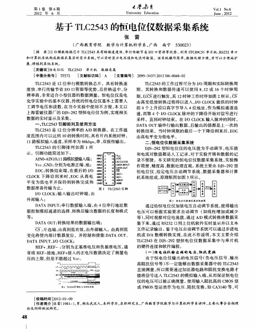
一
T C 5 3的工作过程可分 为 I L 24 / O周期 和实 际转换 周 期 ,其 转换 和数据传 递 可 以使 用 8 1 、2或 1 时钟 周 6个 期, S 以C 进行触 发 , 1 其 2时钟工作时序如图 2所示 。 S C 由高变低 使转换过 程得 以进人 ,O C O K提供 的时钟 I L C / 前 4个上升沿 以高 字节导人 4位地址 , 为模拟 通道选 作 通, 而第 4个 I L C / C O K脉冲的下降沿开始对信 号进行 O 采样 ,直到时钟结束 。在 I L C / C O K输入 脉冲的 同时 , O D T U A A O T端 串行输 出数 据 , 且输 出的值都是上 一次 的 嚣 转换结果 ,当时钟周期 的最后一个 下降沿 到来 后 , O EC 由高 电平变为低 电平 。 二、 电位仪数据采集 系统 恒 D S 2 2型恒 电位仪 的 电压值 为手 动调节 , J一 9 电压值 和电流对数 值都是人工记 录 , 于实验开展 和数 据 的记 对 录不便捷 。本文研究 的恒 电位仪 数据采集 系统 , 实验操
:片选端 , 由高到低有效 , 由外部输入 。由高 到低 变化将使 内部计 数器复位 ,并 控制和使能 D T U A A O T、
作简便 、 高 、 精度 数据处理直观 。 系统主要 由 D S22型 J一9 恒 电位仪 、 给定 电压 自动 调节 系统 、 据采 集器 和计算 数
机 系统组成 , 原理框 图如 图 3 所示 。
展 、 植 到 其 他 系统 。 移
[ 关键词 ] 电位仪 恒
T C 5 3 单片机 L 24
TLC2543在89C51单片机数据采集系统中的应用[1]
![TLC2543在89C51单片机数据采集系统中的应用[1]](https://img.taocdn.com/s3/m/0c732fef102de2bd9605884c.png)
T LC2543在89C51单片机数据采集系统中的应用ΞApplication of T LC2543in MCU Data Acquisition System姚 远1,王 赛2,凌毓涛1(1.华中师范大学信息技术系 湖北武汉430079;2.华中师范大学计算机科学系 湖北武汉430079)【摘 要】 介绍了单片机数据采集系统的硬件原理和软件设计。
该系统以89C51单片机为核心,以12位TLC2543为串行模数转换器,由MC14489构成采集数据实时显示系统,带有RS2232通信接口,系统具有易实现、易编程、可移植、体积小、功耗低等优点,具有良好的推广与应用价值。
关键词:TLC2543,单片机,数据采集【Abstract】 The paper introduces the hardware principle and the software design of the MCU data acquisition system based on89C51,in which the12bit TLC2543acts as the serial A/D converter and the RS2232as the communication interface,and the real2time displaying system is constructed by MC14489. The system has the advantages of easily realize,program and transplant,and it has the small volume and low power,etc..It is therefore very promising and valuable.K eyw ords:TLC2543,MCU,data acquisition1 T LC2543芯片介绍TLC2543是TI公司的具有11个通道的12位开关电容逐次逼近串行A/D转换器,采样率为66kbit/ s,采样和保持由片内采样保持电路自动完成。
基于51单片机TLC2543的AD电压采集双通道12864显示程序

uchar ch,i,j; uint ad; ch=port; for(j=0;j<3;j++) {
ad=0; ch=port; eoc=1; cs=1; cs=0; clk=0; for(i=0;i<12;i++) {
if(sdo) ad|=0x01; sdi=(bit)(ch&0x80); clk=1; clk=0; ch<<=1; ad<<=1;
sbit key1=P3^1; sbit key2=P3^2; sbit key3=P3^3; sbit key4=P3^4; sbit LED=P2^0;
void delay_ms(uchar t) {
uint j,k; for(k=t;k>0;k--)
for(j=110;j>0;j--); }
void write_com(uchar com) {
uchar table[5]; uint sda=8000;
sbit eoc=P1^3; sbit clk=P1^4; sbit sdi=P1^5; sbit sdo=P1^6; sbit cs=P1^7; sbit lcd_rs=P2^4; sbit lcd_rw=P2^5; sbit lcd_en=P2^6; sbit lcd_psb=P2^1; sbit lcd_rst=P2^3;
{
LED=0;
display1(3,0,"电流超出设定值!");
delay_ms(2000);
}
}
else
{
LED=1;
display1(3,0,"
- 1、下载文档前请自行甄别文档内容的完整性,平台不提供额外的编辑、内容补充、找答案等附加服务。
- 2、"仅部分预览"的文档,不可在线预览部分如存在完整性等问题,可反馈申请退款(可完整预览的文档不适用该条件!)。
- 3、如文档侵犯您的权益,请联系客服反馈,我们会尽快为您处理(人工客服工作时间:9:00-18:30)。
//从TLC2543读取采样值,形参port是采样
unsigned int read2543(unsigned char td_num) //对应某通道的A/D转换函数,td_num为通道号{ // 范围为:0~10,对应于0#~10#//
unsigned char addr; // addr为对应某通道号的可编程输入数据//
unsigned char in_8; // in_8为高位或低位的8位A/D转换值//
unsigned char loop; // loop为输出的位数//
unsigned int zz; // zz为A/D转换的中间值和最终值//
bit cc; //89C51的进位位//
cs=1; //令cs=1,即TLC2543处于A/D转换周期//
ad_lp:if(!eoc)goto ad_lp; //在cs=1期间,进行某通道的A/D转换,EOC=1转换结束// addr=td_num*0x10+AD0_D; // td_num为通道号输入参数,addr为对应某通道号的可编程输入数据//
cs=0; //选通TLC2543。
开始I/O周期//
loop=8; //MSB的位数共8位//
in_8=0; //初始化清存贮A/D值的存贮单元//
do{
clk=0; //输出一个CLK的低电平到TLC2543//
cc=out; //把TLC2543的DATA OUT输出至89C51的进位位//
if(cc)in_8=(in_8*2)+0x01; //对A/D值的处理,若本次DA TA OUT的电平为1,则in_8值左移一位后再加1//
else in_8=in_8*2; //若本次DATA OUT的电平为0,则in_8值左移一位//
//以下做可编程数据从89C51向TLC2543的输入寄存器同步输出//
if(addr&0x80)in=1; //若addr的最高位为1,则向TLC2543输出值AD_ADDR=1// else in=0; //若addr的最高位为0,则向TLC2543输出值AD_ADDR=0//
addr<<=1; // addr为可编程数据,左移一位,准备下一位的输出//
clk=1; //输出一个CLK电平1给TLC2543//
}while(--loop); //共做位//
zz= in_8*0x10; // in_8左移4位,in_8为A/D数据的高8位//
//以下做低8位数据从TLC2543向89C51输出//
loop=8;
in_8=0;
do{
clk=0;
cc=out;
if(cc)in_8=(in_8*2)+0x01;
else in_8=in_8*2;
if(addr&0x80)in=1;
else in=0;
addr<<=1;
clk=1;
}while(--loop);
//以下是对高8位和低8位数据合并处理为16位数据//
zz+=in_8/0x10;
clk=0;
cs=1; //重新禁止TLC2543,I/O口线处于高阻状态// return(zz);
}。