TLC2543程序介绍资料
TLC2543 芯片资料
IMPORTANT NOTICETexas Instruments and its subsidiaries (TI) reserve the right to make changes to their products or to discontinue any product or service without notice, and advise customers to obtain the latest version of relevant information to verify, before placing orders, that information being relied on is current and complete. All products are sold subject to the terms and conditions of sale supplied at the time of order acknowledgement, including those pertaining to warranty, patent infringement, and limitation of liability.TI warrants performance of its semiconductor products to the specifications applicable at the time of sale in accordance with TI’s standard warranty. Testing and other quality control techniques are utilized to the extent TI deems necessary to support this warranty. Specific testing of all parameters of each device is not necessarily performed, except those mandated by government requirements.CERTAIN APPLICATIONS USING SEMICONDUCTOR PRODUCTS MAY INVOLVE POTENTIAL RISKS OF DEATH, PERSONAL INJURY, OR SEVERE PROPERTY OR ENVIRONMENTAL DAMAGE (“CRITICAL APPLICATIONS”). TI SEMICONDUCTOR PRODUCTS ARE NOT DESIGNED, AUTHORIZED, OR WARRANTED TO BE SUITABLE FOR USE IN LIFE-SUPPORT DEVICES OR SYSTEMS OR OTHER CRITICAL APPLICATIONS. INCLUSION OF TI PRODUCTS IN SUCH APPLICATIONS IS UNDERSTOOD TO BE FULLY AT THE CUSTOMER’S RISK.In order to minimize risks associated with the customer’s applications, adequate design and operating safeguards must be provided by the customer to minimize inherent or procedural hazards.TI assumes no liability for applications assistance or customer product design. TI does not warrant or represent that any license, either express or implied, is granted under any patent right, copyright, mask work right, or other intellectual property right of TI covering or relating to any combination, machine, or process in which such semiconductor products or services might be or are used. TI’s publication of information regarding any third party’s products or services does not constitute TI’s approval, warranty or endorsement thereof.Copyright © 1998, Texas Instruments Incorporated。
AD转换芯片TLC2543驱动程序

//功能选择关闭
delay1(5);
//AD 转换时间延时
AD_2543_CS=0;;
//功能选择打开
delay1(5);
//建立时间延时
for(circle_temp=0;circle_temp<4;circle_temp++)//读出 12 位数据的 高 4 位数据,存于 temp_h 的低 4 位
test_vl<<=1; if(AD_2543_D_OUT) {
test_vl++; } AD_2543_CLK=1; //时钟上半周期 delay1(2);
AD_2543_CLK=0; } AD_2543_CS=1; ad_value = test_vh; ad_value ห้องสมุดไป่ตู้<= 8; ad_value |= test_vl; return ad_value; }
出的数据是 12 位,D1 为输出的数据是 MSB 为前导,D0 为输出的数
据是无符号二进制数据
AD_2543_CS=1;
//功能选择关闭
delay1(5);
//AD 转换时间延时
AD_2543_CS=0;
//功能选择打开
delay1(5);
//建立时间延时
for(circle_temp=0;circle_temp<12;circle_temp++)//写入十二个数
//下降沿作用,时钟下半周期 //功能选择关闭
#include <reg52.h>
///////////////////////////////////////// //2543 控制引脚宏定义 ////////////////////////////////////////// sbit AD_2543_CLK=P1^0; //2543 时钟/ sbit AD_2543_D_IN=P1^2 ; //2543 输入 sbit AD_2543_D_OUT=P1^1; //2543 输出 sbit AD_2543_CS=P1^3 ; //2543 片选
TLC2543时序图以及程序
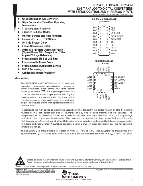
TLC2543引脚说明引脚号名称I/O说明1~9,11,12 AIN0~AIN1I 模拟量输入端。
11路输入信号由内部多路器选通。
对于4.1MHz的I/OCLOCK,驱动源阻抗必须小于或等于50Ω,而且用60pF电容来限制模拟输入电压的斜率15 I 片选端。
在端由高变低时,内部计数器复位。
由低变高时,在设定时间内禁止DATAINPUT和I/O CLOCK17 DATAINPUT I 串行数据输入端。
由4位的串行地址输入来选择模拟量输入通道16 DATA OUT O A/D转换结果的三态串行输出端。
为高时处于高阻抗状态,为低时处于激活状态19 EOC O 转换结束端。
在最后的I/OCLOCK下降沿之后,EOC从高电平变为低电平并保持到转换完成和数据准备传输为止10 GND 地。
GND是内部电路的地回路端。
除另有说明外,所有电压测量都相对GND而言18 I/O CLOCK I 输入/输出时钟端。
I/OCLOCK接收串行输入信号并完成以下四个功能:(1)在I/O CLOCK的前8个上升沿,8位输入数据存入输入数据寄存器。
(2)在I/OCLOCK的第4个下降沿,被选通的模拟输入电压开始向电容器充电,直到I/OCLOCK的最后一个下降沿为止。
(3)将前一次转换数据的其余11位输出到DATAOUT端,在I/OCLOCK的下降沿时数据开始变化。
(4)I/OCLOCK的最后一个下降沿,将转换的控制信号传送到内部状态控制位14 REF+ I 正基准电压端。
基准电压的正端(通常为Vcc)被加到REF+,最大的输入电压范围由加于本端与REF-端的电压差决定13 REF- I 负基准电压端。
基准电压的低端(通常为地)被加到REF-20 Vcc 电源TLC2543接口时序可以用四种传输方法使TLC2543得到全12位分辩率,每次转换和数据传递可以使用12或16个时钟周期。
一个片选()脉冲要插到每次转换的开始处,或是在转换时序的开始处变化一次后保持为低,直到时序结束。
tlc2543中文资料
PACKAGING INFORMATIONOrderable Device Status(1)PackageType PackageDrawingPins PackageQtyEco Plan(2)Lead/Ball Finish MSL Peak Temp(3)5962-9688601QRA ACTIVE CDIP J201TBD A42N/A for Pkg Type TLC2543CDB ACTIVE SSOP DB2070Green(RoHS&no Sb/Br)CU NIPDAU Level-1-260C-UNLIMTLC2543CDBG4ACTIVE SSOP DB2070Green(RoHS&no Sb/Br)CU NIPDAU Level-1-260C-UNLIM TLC2543CDBLE OBSOLETE SSOP DB20TBD Call TI Call TITLC2543CDBR ACTIVE SSOP DB202000Green(RoHS&no Sb/Br)CU NIPDAU Level-1-260C-UNLIMTLC2543CDBRG4ACTIVE SSOP DB202000Green(RoHS&no Sb/Br)CU NIPDAU Level-1-260C-UNLIMTLC2543CDW ACTIVE SOIC DW2025Green(RoHS&no Sb/Br)CU NIPDAU Level-1-260C-UNLIMTLC2543CDWG4ACTIVE SOIC DW2025Green(RoHS&no Sb/Br)CU NIPDAU Level-1-260C-UNLIMTLC2543CDWR ACTIVE SOIC DW202000Green(RoHS&no Sb/Br)CU NIPDAU Level-1-260C-UNLIMTLC2543CDWRG4ACTIVE SOIC DW202000Green(RoHS&no Sb/Br)CU NIPDAU Level-1-260C-UNLIMTLC2543CFN ACTIVE PLCC FN2046Green(RoHS&no Sb/Br)CU SN Level-1-260C-UNLIMTLC2543CFNG3ACTIVE PLCC FN2046Green(RoHS&no Sb/Br)CU SN Level-1-260C-UNLIMTLC2543CFNR ACTIVE PLCC FN201000Green(RoHS&no Sb/Br)CU SN Level-1-260C-UNLIMTLC2543CFNRG3ACTIVE PLCC FN201000Green(RoHS&no Sb/Br)CU SN Level-1-260C-UNLIMTLC2543CN ACTIVE PDIP N2020Pb-Free(RoHS)CU NIPDAU N/A for Pkg TypeTLC2543CNE4ACTIVE PDIP N2020Pb-Free(RoHS)CU NIPDAU N/A for Pkg TypeTLC2543IDB ACTIVE SSOP DB2070Green(RoHS&no Sb/Br)CU NIPDAU Level-1-260C-UNLIMTLC2543IDBG4ACTIVE SSOP DB2070Green(RoHS&no Sb/Br)CU NIPDAU Level-1-260C-UNLIMTLC2543IDBR ACTIVE SSOP DB202000Green(RoHS&no Sb/Br)CU NIPDAU Level-1-260C-UNLIMTLC2543IDBRG4ACTIVE SSOP DB202000Green(RoHS&no Sb/Br)CU NIPDAU Level-1-260C-UNLIMTLC2543IDW ACTIVE SOIC DW2025Green(RoHS&no Sb/Br)CU NIPDAU Level-1-260C-UNLIMTLC2543IDWG4ACTIVE SOIC DW2025Green(RoHS&no Sb/Br)CU NIPDAU Level-1-260C-UNLIMTLC2543IDWR ACTIVE SOIC DW202000Green(RoHS&no Sb/Br)CU NIPDAU Level-1-260C-UNLIMTLC2543IDWRG4ACTIVE SOIC DW202000Green(RoHS&no Sb/Br)CU NIPDAU Level-1-260C-UNLIMTLC2543IFN ACTIVE PLCC FN2046Green(RoHS&no Sb/Br)CU SN Level-1-260C-UNLIMTLC2543IFNG3ACTIVE PLCC FN2046Green(RoHS&CU SN Level-1-260C-UNLIMOrderable Device Status(1)PackageType PackageDrawingPins PackageQtyEco Plan(2)Lead/Ball Finish MSL Peak Temp(3)no Sb/Br)TLC2543IFNR OBSOLETE PLCC FN20TBD Call TI Call TITLC2543IN ACTIVE PDIP N2020Pb-Free(RoHS)CU NIPDAU N/A for Pkg TypeTLC2543INE4ACTIVE PDIP N2020Pb-Free(RoHS)CU NIPDAU N/A for Pkg Type TLC2543MJ ACTIVE CDIP J201TBD A42N/A for Pkg Type TLC2543MJB ACTIVE CDIP J201TBD A42N/A for Pkg Type (1)The marketing status values are defined as follows:ACTIVE:Product device recommended for new designs.LIFEBUY:TI has announced that the device will be discontinued,and a lifetime-buy period is in effect.NRND:Not recommended for new designs.Device is in production to support existing customers,but TI does not recommend using this part in a new design.PREVIEW:Device has been announced but is not in production.Samples may or may not be available.OBSOLETE:TI has discontinued the production of the device.(2)Eco Plan-The planned eco-friendly classification:Pb-Free(RoHS),Pb-Free(RoHS Exempt),or Green(RoHS&no Sb/Br)-please check /productcontent for the latest availability information and additional product content details.TBD:The Pb-Free/Green conversion plan has not been defined.Pb-Free(RoHS):TI's terms"Lead-Free"or"Pb-Free"mean semiconductor products that are compatible with the current RoHS requirements for all6substances,including the requirement that lead not exceed0.1%by weight in homogeneous materials.Where designed to be soldered at high temperatures,TI Pb-Free products are suitable for use in specified lead-free processes.Pb-Free(RoHS Exempt):This component has a RoHS exemption for either1)lead-based flip-chip solder bumps used between the die and package,or2)lead-based die adhesive used between the die and leadframe.The component is otherwise considered Pb-Free(RoHS compatible)as defined above.Green(RoHS&no Sb/Br):TI defines"Green"to mean Pb-Free(RoHS compatible),and free of Bromine(Br)and Antimony(Sb)based flame retardants(Br or Sb do not exceed0.1%by weight in homogeneous material)(3)MSL,Peak Temp.--The Moisture Sensitivity Level rating according to the JEDEC industry standard classifications,and peak solder temperature.Important Information and Disclaimer:The information provided on this page represents TI's knowledge and belief as of the date that it is provided.TI bases its knowledge and belief on information provided by third parties,and makes no representation or warranty as to the accuracy of such information.Efforts are underway to better integrate information from third parties.TI has taken and continues to take reasonable steps to provide representative and accurate information but may not have conducted destructive testing or chemical analysis on incoming materials and chemicals.TI and TI suppliers consider certain information to be proprietary,and thus CAS numbers and other limited information may not be available for release.In no event shall TI's liability arising out of such information exceed the total purchase price of the TI part(s)at issue in this document sold by TI to Customer on an annual basis.OTHER QUALIFIED VERSIONS OF TLC2543,TLC2543M:•Automotive:TLC2543-Q1•Enhanced Product:TLC2543-EPNOTE:Qualified Version Definitions:•Automotive-Q100devices qualified for high-reliability automotive applications targeting zero defects•Enhanced Product-Supports Defense,Aerospace and Medical ApplicationsTAPE AND REEL INFORMATION*All dimensions are nominalDevicePackage Type Package Drawing Pins SPQReel Diameter (mm)Reel Width W1(mm)A0(mm)B0(mm)K0(mm)P1(mm)W (mm)Pin1Quadrant TLC2543CDBR SSOP DB 202000330.016.48.27.5 2.512.016.0Q1TLC2543IDBRSSOPDB202000330.016.48.27.52.512.016.0Q1*All dimensions are nominalDevice Package Type Package Drawing Pins SPQ Length(mm)Width(mm)Height(mm) TLC2543CDBR SSOP DB202000346.0346.033.0TLC2543IDBR SSOP DB202000346.0346.033.0IMPORTANT NOTICETexas Instruments Incorporated and its subsidiaries(TI)reserve the right to make corrections,modifications,enhancements,improvements, and other changes to its products and services at any time and to discontinue any product or service without notice.Customers should obtain the latest relevant information before placing orders and should verify that such information is current and complete.All products are sold subject to TI’s terms and conditions of sale supplied at the time of order acknowledgment.TI warrants performance of its hardware products to the specifications applicable at the time of sale in accordance with TI’s standard warranty.Testing and other quality control techniques are used to the extent TI deems necessary to support this warranty.Except where mandated by government requirements,testing of all parameters of each product is not necessarily performed.TI assumes no liability for applications assistance or customer product design.Customers are responsible for their products and applications using TI components.To minimize the risks associated with customer products and applications,customers should provide adequate design and operating safeguards.TI does not warrant or represent that any license,either express or implied,is granted under any TI patent right,copyright,mask work right, or other TI intellectual property right relating to any combination,machine,or process in which TI products or services are rmation published by TI regarding third-party products or services does not constitute a license from TI to use such products or services or a warranty or endorsement e of such information may require a license from a third party under the patents or other intellectual property of the third party,or a license from TI under the patents or other intellectual property of TI.Reproduction of TI information in TI data books or data sheets is permissible only if reproduction is without alteration and is accompanied by all associated warranties,conditions,limitations,and notices.Reproduction of this information with alteration is an unfair and deceptive business practice.TI is not responsible or liable for such altered rmation of third parties may be subject to additional restrictions.Resale of TI products or services with statements different from or beyond the parameters stated by TI for that product or service voids all express and any implied warranties for the associated TI product or service and is an unfair and deceptive business practice.TI is not responsible or liable for any such statements.TI products are not authorized for use in safety-critical applications(such as life support)where a failure of the TI product would reasonably be expected to cause severe personal injury or death,unless officers of the parties have executed an agreement specifically governing such use.Buyers represent that they have all necessary expertise in the safety and regulatory ramifications of their applications,and acknowledge and agree that they are solely responsible for all legal,regulatory and safety-related requirements concerning their products and any use of TI products in such safety-critical applications,notwithstanding any applications-related information or support that may be provided by TI.Further,Buyers must fully indemnify TI and its representatives against any damages arising out of the use of TI products in such safety-critical applications.TI products are neither designed nor intended for use in military/aerospace applications or environments unless the TI products are specifically designated by TI as military-grade or"enhanced plastic."Only products designated by TI as military-grade meet military specifications.Buyers acknowledge and agree that any such use of TI products which TI has not designated as military-grade is solely at the Buyer's risk,and that they are solely responsible for compliance with all legal and regulatory requirements in connection with such use. TI products are neither designed nor intended for use in automotive applications or environments unless the specific TI products are designated by TI as compliant with ISO/TS16949requirements.Buyers acknowledge and agree that,if they use any non-designated products in automotive applications,TI will not be responsible for any failure to meet such requirements.Following are URLs where you can obtain information on other Texas Instruments products and application solutions:Products ApplicationsAmplifiers AudioData Converters AutomotiveDLP®Products BroadbandDSP Digital ControlClocks and Timers MedicalInterface MilitaryLogic Optical NetworkingPower Mgmt SecurityMicrocontrollers TelephonyRFID Video&ImagingRF/IF and ZigBee®Solutions WirelessMailing Address:Texas Instruments,Post Office Box655303,Dallas,Texas75265Copyright©2009,Texas Instruments Incorporated。
TLC2543应用
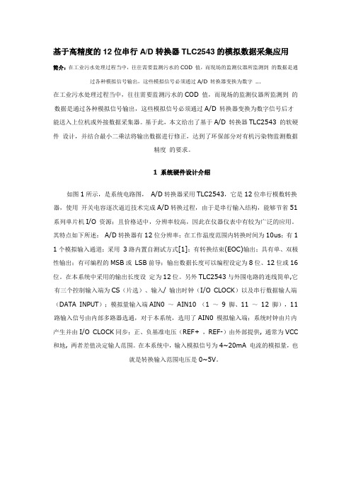
基于高精度的12位串行A/D转换器TLC2543的模拟数据采集应用简介:在工业污水处理过程当中,往往需要监测污水的COD 值,而现场的监测仪器所监测到的数据是通过各种模拟信号输出,这些模拟信号必须通过A/D 转换器变换为数字 ...在工业污水处理过程当中,往往需要监测污水的COD 值,而现场的监测仪器所监测到的数据是通过各种模拟信号输出,这些模拟信号必须通过A/D 转换器变换为数字信号后才能送入上位机或外接数据采集器。
基于此,本文给出了基于A/D 转换器TLC2543 的软硬件设计,并结合最小二乘法将输出数据进行修正,达到了环保部分对有机污染物监测数据精度的要求。
1 系统硬件设计介绍如图1所示,是系统电路图,A/D转换器采用TLC2543,它是12位串行模数转换器,使用开关电容逐次逼近技术完成A/D转换过程,由于是串行输入结构,能够节省51系列单片机I/O 资源;且价格适中,分辨率较高,因此在仪器仪表中有较为广泛的应用。
其特点如下所述:A/D转换器有12位分辨率;在工作温度范围内转换时间为10us;有1 1个模拟输入通道;采用3路内置自测试方式[1];有转换结束(EOC)输出;具有单、双极性输出;有可编程的MSB或LSB前导;输出数据长度可以编程设定为8位、12位或16位。
在本系统中采用的输出长度设定为12位。
另外TLC2543与外围电路的连线简单,它有三个控制输入端为CS(片选)、输入/ 输出时钟(I/O CLOCK)以及串行数据输人端(DATA INPUT);模拟量输入端AIN0 ~AIN10 (1 ~9 脚、11 ~12 脚),11路输入信号由内部多路器选通,对于本系统,选用了AIN0 模拟输入端;系统时钟由片内产生并由I/O CLOCK同步;正、负基准电压(REF+ ,REF-)由外部提供, 通常为VCC 和地, 两者差值决定输人范围。
在本系统中,输入模拟信号为4~20mA 电流的模拟量,也就是转换输入范围电压是0~5V。
TLC2543程序

//========================================================== ===========// tlc2543驱动程序//tlc2543.c//writer:谷雨2008年3月12日于EDA实验室整理//========================================================== ===========#include#define uint unsigned int#define uchar unsigned char//**************************修改硬件时要修改的部分********************************sbit clock = P0^0; //输入、输出时钟端sbit input = P0^1; //数据输入端sbit output = P0^2; //数据输出端sbit CS = P0^3; //片选端,负电平有效void delay(uchar N){while(N--);}uint read2543(uchar CON_WORD) //CON_WORD为选择的通道,为0--10 {uint ad=0;uchar i;CON_WORD<<=4;clock=0;CS=0;for(i=0;i<12;i++){if(output==1) //读取DATAOUTad=ad|0x01;if(CON_WORD&0x80) //读取控制字到INPUTinput=1;elseinput=0;clock=1;delay(10);clock=0;delay(10);CON_WORD<<=1;ad<<=1;}CS=1;ad>>=1;return(ad);}void init_serial() //初始化串口{TMOD=0x20; //定时器T1使用工作方式2TH1=250; //设置初值TH0=250;TR1=1; //开始计时PCON=0x80; //SMOD=1;SCON=0x50; //工作方式1,波特率9600bit/s,允许接收TI=1;}void main(){uint ad=0;float fVoltage1;uchar buf[5],i;init_serial();IE=0; //屏蔽中断while(1){ad=read2543(0);fVoltage1=(float)ad/0x0fff*5;buf[0]=(uchar)fVoltage1;buf[0]=buf[0]+0x30;buf[1]=''.'buf[2]=(uchar)(fVoltage1*10)%10;buf[2]=buf[2]+0x30;buf[3]=(uchar)(fVoltage1*100-buf[0]*100)%10;buf[3]=buf[3]+0x30;buf[4]=(uchar)((fVoltage1*1000)-buf[0]*1000-buf[1]*100)%10; buf[4]=buf[4]+0x30;i=0;while(i<5){if(TI==1){SBUF=buf[i];TI=0;i++;}}} }。
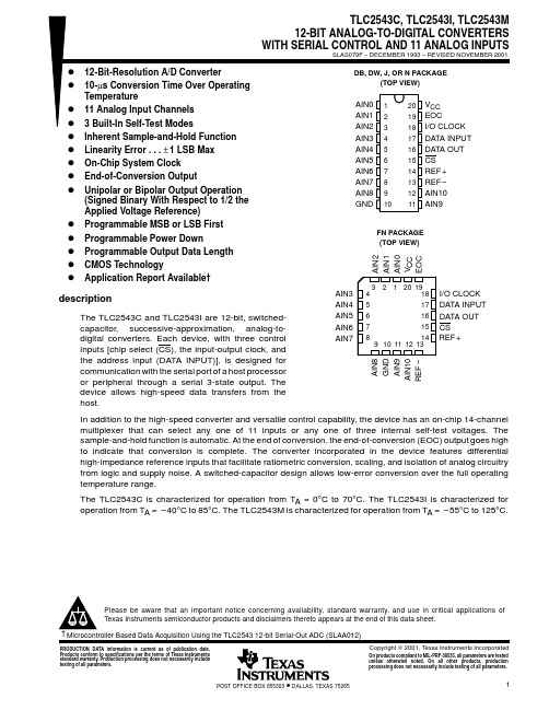
TLC2543引脚、功能及时序

TLC2543引脚、功能及时序一、模块采用TI公司的TLC2543 12位串行A/D转换器,使用开关电容逐次逼近技术完成A/D 转换过程。
由于是串行输入结构,能够节省51 系列单片机I/O 资源,且价格适中。
其特点有:(1)12位分辨率A/D转换器;(2)在工作温度范围内10 ys转换时间;( 3) 11 个模拟输入通道;( 4) 3 路内置自测试方式;( 5)采样率为66kbps ;( 6)线性误差+1LSB (max)(7)有转换结束(EOC)输出;( 8)具有单、双极性输出;( 9)可编程的MSB 或LSB 前导;( 10)可编程的输出数据长度。
二、TLC2543 的引脚排列如图所示。
1~9、11、12 —— AIN0〜AIN10为模拟输入端;15 ——CS 为片选端;17——DIN 为串行数据输入端;(控制字输入端,用于选择转换及输出数据格式) 16——DOUT 为A/D 转换结果的三态串行输出端;( A/D 转换结果的输出端。
)19 ——EOC 为转换结束端;18——CLK 为I/O 时钟;(控制输入输出的时钟,由外部输入。
)14 —— REF+为正基准电压端;13 ―― REF-为负基准电压端;20——VCC 为电源;10 ―― GND 为地。
三、TLC2543的使用方法3. 1控制字的格式控制字为从DATAINPUT 端串行输入的8位数据,它规定了 TLC2543要转换的 模拟量通道、转换后的输出数据长度、输出数据的格式。
高4位(D7〜D4)决定通道号,对于0通道至10通道,该4位分别为0000〜1010H ,当为1011〜1101时,用于对TLC2543的自检,分别测试(VREF + + VREF— )/2、VREF ―、VREF + 的值,当为 1110 时,TLC2543 进入休眠状态。
低4位决定输出数据长度及格式,D3、D2决定输出数据长度,01表示输出数据长度为8位,11表示输出数 据长度为16位,其他为12位。
TLC2543

摘要:TLC2543是德州仪器公司生产的12位开关电容型逐次逼近模数转换器,它具有三个控制输入端,采用简单的3线SPI串行接口可方便地与微机进行连接,是12位数据采集系统的最佳选择器件之一。
本文介绍了该芯片的功能、时序,并给出了8051单片机的接口电路。
关键词:模数转换器; SPI串行接口; TLC25431. 概述A/D、D/A转换器是过程及仪器仪表、设备等检测与控制装置中应用比较广泛的器件。
随着大规模集成电路技术的发展,各种高精度、低功耗、可编程、低成本的A/D转换器不断推出,使得微机控制系统的电路更加简洁,可靠性更高。
TLC2543与外围电路的连线简单,三个控制输入端为CS(片选)、输入/输出时钟(I/O CLOCK)以及串行数据输入端(DATA INPUT)。
片内的14通道多路器可以选择11个输入中的任何一个或3个内部自测试电压中的一个,采样-保持是自动的,转换结束,EOC输出变高。
TLC2543的主要特性如下:●11个模拟输入通道;●66ksps的采样速率;●最大转换时间为10μs;●SPI串行接口;●线性度误差最大为±1LSB;●低供电电流(1mA典型值);●掉电模式电流为4μA。
2. TLC2543引脚功能与接口时序2.1 TLC2543引脚排列TLC2543的引脚排列如图1所示。
引脚功能说明如下:AIN0~AIN10:模拟输入端,由内部多路器选择。
对4.1MHz的I/O CLOCK,驱动源阻抗必须小于或等于50Ω;CS:片选端,CS由高到低变化将复位内部计数器,并控制和使能DATA OUT、DATA INPUT 和I/O CLOCK。
CS由低到高的变化将在一个设置时间内禁止DATA INPUT和I/O CLOCK;DATA INPUT:串行数据输入端,串行数据以MSB为前导并在I/O CLOCK的前4个上升沿移入4位地址,用来选择下一个要转换的模拟输入信号或测试电压,之后I/O CLOCK将余下的几位依次输入;DATA OUT:A/D转换结果三态输出端,在CS为高时,该引脚处于高阻状态;当CS为低时,该引脚由前一次转换结果的MSB值置成相应的逻辑电平;EOC:转换结束端。
TLC2543 中文资料

TLC2543 中文资料TLC2543是TI公司的12位串行模数转换器,使用开关电容逐次逼近技术完成A/D转换过程。
由于是串行输入结构,能够节省51系列单片机I/O资源;且价格适中,分辨率较高,因此在仪器仪表中有较为广泛的应用。
2 TLC254 ...TLC2543是TI公司的12位串行模数转换器,使用开关电容逐次逼近技术完成A/D 转换过程。
由于是串行输入结构,能够节省51系列单片机I/O资源;且价格适中,分辨率较高,因此在仪器仪表中有较为广泛的应用。
2 TLC2543的特点(1)12位分辩率A/D转换器;(2)在工作温度范围内10μs转换时间;(3)11个模拟输入通道;(4)3路内置自测试方式;(5)采样率为66kbps;(6)线性误差±1LSBmax;(7)有转换结束输出EOC;(8)具有单、双极性输出;(9)可编程的MSB或LSB前导;(10)可编程输出数据长度。
3TLC2543的引脚图(管脚图)及说明TLC2543有两种封装形式:DB、DW或N封装以及FN封装,这两种封装的引脚排列如图1,引脚说明见表1。
表1 TLC2543引脚说明引脚号名称I/O 说明1~9,11,12 AIN0~AIN10 I 模拟量输入端。
11路输入信号由内部多路器选通。
对于4.1MHz的I/OCLOCK,驱动源阻抗必须小于或等于50Ω,而且用60pF电容来限制模拟输入电压的斜率15 I 片选端。
在端由高变低时,内部计数器复位。
由低变高时,在设定时间内禁止DATAINPUT和I/O CLOCK17 DATAINPUT I 串行数据输入端。
由4位的串行地址输入来选择模拟量输入通道16 DATA OUT O A/D转换结果的三态串行输出端。
为高时处于高阻抗状态,为低时处于激活状态19 EOC O 转换结束端。
在最后的I/OCLOCK下降沿之后,EOC从高电平变为低电平并保持到转换完成和数据准备传输为止10 GND 地。
TLC2543采集程序

TLC2543采集程序//从TLC2543读取采样值,形参port是采样unsigned int read2543(unsigned char td_num) //对应某通道的A/D转换函数,td_num为通道号{ // 范围为:0~10,对应于0#~10#//unsigned char addr; // addr为对应某通道号的可编程输入数据//unsigned char in_8; // in_8为高位或低位的8位A/D转换值// unsigned char loop; // loop为输出的位数//unsigned int zz; // zz为A/D转换的中间值和最终值//bit cc; //89C51的进位位//cs=1; //令cs=1,即TLC2543处于A/D转换周期//ad_lp:if(!eoc)goto ad_lp; //在cs=1期间,进行某通道的A/D转换,EOC=1转换结束// addr=td_num*0x10+AD0_D; // td_num为通道号输入参数,addr为对应某通道号的可编程输入数据// cs=0; //选通TLC2543。
开始I/O周期//loop=8; //MSB的位数共8位//in_8=0; //初始化清存贮A/D值的存贮单元//do{clk=0; //输出一个CLK的低电平到TLC2543//cc=out; //把TLC2543的DATA OUT输出至89C51的进位位// if(cc)in_8=(in_8*2)+0x01; //对A/D值的处理,若本次DA TA OUT的电平为1,则in_8值左移一位后再加1//else in_8=in_8*2; //若本次DATA OUT的电平为0,则in_8值左移一位////以下做可编程数据从89C51向TLC2543的输入寄存器同步输出//if(addr&0x80)in=1; //若addr的最高位为1,则向TLC2543输出值AD_ADDR=1// else in=0; //若addr的最高位为0,则向TLC2543输出值AD_ADDR=0//addr<<=1; // addr为可编程数据,左移一位,准备下一位的输出//clk=1; //输出一个CLK电平1给TLC2543//}while(--loop); //共做位//zz= in_8*0x10; // in_8左移4位,in_8为A/D数据的高8位// //以下做低8位数据从TLC2543向89C51输出//loop=8;in_8=0;do{clk=0;cc=out;if(cc)in_8=(in_8*2)+0x01;else in_8=in_8*2;if(addr&0x80)in=1;else in=0;addr<<=1;clk=1;}while(--loop);//以下是对高8位和低8位数据合并处理为16位数据//zz+=in_8/0x10;clk=0;cs=1; //重新禁止TLC2543,I/O口线处于高阻状态// return(zz);}。
TLC2543中文资料_数据手册_参数

万联芯城专注电子元器件配单服务,只售原装现货库存,万联芯城 电子元器件全国供应,专为终端生产,研发企业提供现货物料, 价格优势明显,BOM配单整单采购可享优惠价,提交BOM表报价 ,最快可当天发货,万联芯城电子元器件配单服务可以为客户节 省采购成本,满足客户物料需求,丰富的电子元器件供应链体系 已为全国多家终端企业服务,点击进入万联芯城。
合格的汽车ApplicationsD 12位分辨率A / D ConverterD 10-µs转换时间在OperatingTemperatureD 11模拟输入ChannelsD三内建自测ModesD固 有取样保持的FunctionD线性误差。±1 LSB MaxD片上TLC2543系统ClockD转换末尾OutputD单极或双极输出操作(签署二进制对1/2 theApplied参考电压)D可编程MSB和LSB FirstD可编程电源DownD可编程输出数据LengthD CMOS TechnologyD申请报告可用‡ descriptionThe TLC2543 12位,开关电容,逐次逼近,数模转换器。每台设备有三个控制输入(芯片选择(CS)、输入-输出时钟和地址输入(数据 输入)),通过串行三态输出与主机处理器或外围设备的串口通信。该设备允许从主机高速传输数据。除了高速转换器和多用途控制能 力,该设备还有一个芯片上的14通道多路复用器,可以选择11个输入中的任意一个或3个内部自检电压中的任意一个。这个功能是自动 的。在转换结束时,转换结束(EOC)输出变高,表示转换已经完成。TLC2543集成在器件中的转换器具有不同的高阻抗参考输入,便于 比值转换、缩放和模拟电路与逻辑和电源噪声隔离。开关电容设计允许在整个工作温度范围内的低误差转换。订货信息工作原理首先, 芯片选择(CS)高,I/O时钟和数据输入被禁用,TLC2543数据输出处于高阻抗状态。CS低电平通过启用I/O时钟和数据输入开始转换序 列,并从高阻抗状态中删除数据。输入数据为8位数据流,包括4位模拟信道地址(D7−D4)、2位数据纵向选择(D3−D2)、输出MSB或LSB 第一个位(D1)和应用于数据输入的单极或双极输出选择位(D0)。TLC2543应用于I/O时钟终端的I/O时钟序列将此数据传输到输入数据寄 存器。在这个传输过程中,I/O时钟序列还将之前的转换结果从输出数据寄存器转移到数据输出。I/O时钟接收8、12或16个时钟周期长 的输入序列,这取决于输入数据寄存器中的数据长度选择。TLC2543模拟输入的采样从输入I/O时钟序列的第四个下降沿开始,并在I/O 时钟序列的最后一个下降沿之后进行。I/O时钟序列的最后一个下降沿也将EOC降低并开始转换。转换器的操作转换器的操作被组织成 两个不同的周期的序列:1)I/O周期和2)实际的转换周期。I/O周期I/O周期由外部提供的I/O时钟定义,持续8、12或16个时钟周期,取决于 所选输出数据的长度。在I/O周期中,同时执行以下两个操作。一个由地址和控制信息组成的8位数据流被提供给数据输入。这些数据被 转移到前八个I/O时钟上升边缘的设备中。在12或16个时钟的I/O传输过程中,第一个时钟后的数据输入将被忽略。数据输出(长度为 8、12或16位)是在数据输出时串行提供的。当CS值较低时,第一个输出数据位出现在EOC上升沿。当CS在两次转换之间被否定时,第 一个outputdata位出现在CS的下降边缘。该数据是前一个转换周期的结果,在第一个输出数据位之后,每个后续的位都被锁定在每个后 续I/O时钟的下降边缘。转换周期转换周期对用户是透明的,它由一个内部时钟同步toI/O时钟控制。在转换期间,该装置对模拟输入电 压进行逐次近似转换。EOC输出在转换周期开始时较低,在转换完成并锁定输出数据寄存器时较高。转换周期只有在I/Ocycle完成后才 开始,这样可以将外部数字噪声对转换精度的影响降到最低。
TLC2543中文数据手册

TLC2543使用手册一、简要说明:TLC2543是一款8位、10位、12位为一体的可选输出位数的11通道串行转换芯片。
每一路转换时间为10us。
外部输入信号为:DATA input ;_CS;AD_IO_CLK;Analog input;四种信号;输出为:EOC转换结束信号,DATA output信号。
工作原理为:_CS由高变为低时候,允许DATA input;AD_IO_CLK;Analog input信号输入,DATA out 信号输出;由低到高禁止DATA input;AD_IO_CLK;信号输入。
当忽略ADC转换启动的CS时候,数据的输出是在CS的下降沿,既是将片选的时候,而考虑到CS时候,第一个输出数据发生在EOC变为高的时候的上升沿。
注意:初始化时候,必须将CS由高拉低才能进行数据输出或者是数据输入。
也就是说,当一次转换完成后,进行下一次或者是下一个通道的转换,需要将CS由低拉高,为下一次转换做好准备,当进行下一个转换时候,进行CS 拉低,DATA input输入或者DATA out输出(忽略CS转换作用时候)。
信号解释:DATA input:4位串行地址输入,用来选择模拟输入通道功能或者测试引脚;高位在前,在每一个AD_IO_CLK的上升沿输入ADC的寄存器。
由八位组成:前四位:D7:D4用作选择模拟输入通道,D3:D2用作选择数据长度,D1是选择输出高低位顺序的,D0选择是选择输出极性(单双极性)。
DA TA INPUT的表含义DATA OUT:当_CS为高时DATA out输出为高阻抗,当CS有效时,驱动转换结果,并在AD_IO_CLK的下降沿按位顺序输出。
EOC:ADC的EOC在DATA input输入的最后一个AD_IO_CLK时,由高变为低,并保持到转换结束和数据准备输出结束时候变为高。
AD_IO_CLK:输入和输出时钟,主要完成以下功能:A、在IO_CLK的前八个时钟的上升沿将DATA input的八位数据输入数据寄存器中。
TLC2543资料c语言

2.2TLC2543的内部寄存器
从编程角度看,TLC2543内部寄存器有输入数据寄存器与输出数据寄存器。输入数据寄存器存放从DATA INPUT端移入的控制字。输出数据寄存器存放转换好的数据,以供从DATA OUT端移出。
(4)控制字输入引脚
DATA TNPUT,17脚:控制字输入端,选择通道及输出数据格式的控制字由此输入。
(5)转换数据输出引脚
DATA OUT,16脚:A/D转换结果输出的3态串行输出端。
2TLC2543的编程要点
2.1控制字的格式
控制字为从DATA INPUT端串行输入TLC2543芯片内部的8位数据,它告诉TLC2543要转换的模拟量通道、转换后的输出数据长度、输出数据的格式。其中高4位(D7~D4)决定通道号,对于0通道至10通道,该4位分别为0000、0001、…、1010,该4位为其它数字时的功能,用于检测校正,本文不作具体介绍。低4位决定输出数据长度及格式,其中D3、D2决定输出数据长度,TLC2543的输出数据长度有8位、12位、16位,但由于TLC2543为12位A/D转换芯片,经过分析可以看出,8位、16位输出对TLC2543的应用意义不大,宜定在12位输出,D3、D2两位为00即可。D1决定输出数据是高位先送出,还是低位先送出,若为高位先送出,该位为0,反之为1。D0决定输出数据是单极性(二进制)还是双极性(2的补码),若为单极性,该位为0,反之为1。
关键词:A/D转换;TLC2543芯片;51系列单片机;接口技术
中图法分类号:TP334.7文献识别码:B
TLC2543中文资料

串行A D转换器T L C2543中文资料T L C2543是T I公司的12位串行模数转换器,使用开关电容逐次逼近技术完成A/D转换过程。
由于是串行输入结构,能够节省51系列单片机I/O资源;且价格适中,分辨率较高,因此在仪器仪表中有较为广泛的应用。
2T L C2543的特点(1)12位分辩率A/D转换器;(2)在工作温度范围内10μs转换时间;(3)11个模拟输入通道;(4)3路内置自测试方式;(5)采样率为66k b p s;(6)线性误差±1L S B m a x;(7)有转换结束输出E O C;(8)具有单、双极性输出;(9)可编程的M S B或L S B前导;(10)可编程输出数据长度。
3T L C2543的引脚排列及说明T L C2543有两种封装形式:D B、D W或N封装以及F N封装,这两种封装的引脚排列如图1,引脚说明见表1。
图1T L C2543的封装4接口时序可以用四种传输方法使T L C2543得到全12位分辩率,每次转换和数据传递可以使用12或16个时钟周期。
一个片选()脉冲要插到每次转换的开始处,或是在转换时序的开始处变化一次后保持为低,直到时序结束。
图2显示每次转换和数据传递使用16个时钟周期和在每次传递周期之间插入的时序,图3显示每次转换和数据传递使用16个时钟周期,仅在每次转换序列开始处插入一次时序。
引脚号名称I/O说明1~9,11,12AIN0~AIN10I模拟量输入端。
11路输入信号由内部多路器选通。
对于4.1MHz的I/OCLOCK,驱动源阻抗必须小于或等于50Ω,而且用60pF电容来限制模拟输入电压的斜率15I片选端。
在端由高变低时,内部计数器复位。
由低变高时,在设定时间内禁止DATAINPUT和I/O CLOCK17DATAINPUT I串行数据输入端。
由4位的串行地址输入来选择模拟量输入通道16DATA OUT O A/D转换结果的三态串行输出端。
TLC2543在89C51单片机数据采集系统中的应用[1]
![TLC2543在89C51单片机数据采集系统中的应用[1]](https://img.taocdn.com/s3/m/0c732fef102de2bd9605884c.png)
T LC2543在89C51单片机数据采集系统中的应用ΞApplication of T LC2543in MCU Data Acquisition System姚 远1,王 赛2,凌毓涛1(1.华中师范大学信息技术系 湖北武汉430079;2.华中师范大学计算机科学系 湖北武汉430079)【摘 要】 介绍了单片机数据采集系统的硬件原理和软件设计。
该系统以89C51单片机为核心,以12位TLC2543为串行模数转换器,由MC14489构成采集数据实时显示系统,带有RS2232通信接口,系统具有易实现、易编程、可移植、体积小、功耗低等优点,具有良好的推广与应用价值。
关键词:TLC2543,单片机,数据采集【Abstract】 The paper introduces the hardware principle and the software design of the MCU data acquisition system based on89C51,in which the12bit TLC2543acts as the serial A/D converter and the RS2232as the communication interface,and the real2time displaying system is constructed by MC14489. The system has the advantages of easily realize,program and transplant,and it has the small volume and low power,etc..It is therefore very promising and valuable.K eyw ords:TLC2543,MCU,data acquisition1 T LC2543芯片介绍TLC2543是TI公司的具有11个通道的12位开关电容逐次逼近串行A/D转换器,采样率为66kbit/ s,采样和保持由片内采样保持电路自动完成。
基于51单片机TLC2543的AD电压采集双通道12864显示程序

uchar ch,i,j; uint ad; ch=port; for(j=0;j<3;j++) {
ad=0; ch=port; eoc=1; cs=1; cs=0; clk=0; for(i=0;i<12;i++) {
if(sdo) ad|=0x01; sdi=(bit)(ch&0x80); clk=1; clk=0; ch<<=1; ad<<=1;
sbit key1=P3^1; sbit key2=P3^2; sbit key3=P3^3; sbit key4=P3^4; sbit LED=P2^0;
void delay_ms(uchar t) {
uint j,k; for(k=t;k>0;k--)
for(j=110;j>0;j--); }
void write_com(uchar com) {
uchar table[5]; uint sda=8000;
sbit eoc=P1^3; sbit clk=P1^4; sbit sdi=P1^5; sbit sdo=P1^6; sbit cs=P1^7; sbit lcd_rs=P2^4; sbit lcd_rw=P2^5; sbit lcd_en=P2^6; sbit lcd_psb=P2^1; sbit lcd_rst=P2^3;
{
LED=0;
display1(3,0,"电流超出设定值!");
delay_ms(2000);
}
}
else
{
LED=1;
display1(3,0,"
- 1、下载文档前请自行甄别文档内容的完整性,平台不提供额外的编辑、内容补充、找答案等附加服务。
- 2、"仅部分预览"的文档,不可在线预览部分如存在完整性等问题,可反馈申请退款(可完整预览的文档不适用该条件!)。
- 3、如文档侵犯您的权益,请联系客服反馈,我们会尽快为您处理(人工客服工作时间:9:00-18:30)。
//========================================================== ===========
// tlc2543驱动程序
//tlc2543.c
//writer:谷雨2008年3月12日于EDA实验室整理
//========================================================== ===========
#include
#define uint unsigned int
#define uchar unsigned char
//**************************修改硬件时要修改的部分********************************
sbit clock = P0^0; //输入、输出时钟端
sbit input = P0^1; //数据输入端
sbit output = P0^2; //数据输出端
sbit CS = P0^3; //片选端,负电平有效
void delay(uchar N)
{
while(N--);
}
uint read2543(uchar CON_WORD) //CON_WORD为选择的通道,为0--10 {
uint ad=0;
uchar i;
CON_WORD<<=4;
clock=0;
CS=0;
for(i=0;i<12;i++)
{
if(output==1) //读取DATAOUT
ad=ad|0x01;
if(CON_WORD&0x80) //读取控制字到INPUT
input=1;
else
input=0;
clock=1;
delay(10);
clock=0;
delay(10);
CON_WORD<<=1;
ad<<=1;
}
CS=1;
ad>>=1;
return(ad);
}
void init_serial() //初始化串口
{
TMOD=0x20; //定时器T1使用工作方式2
TH1=250; //设置初值
TH0=250;
TR1=1; //开始计时
PCON=0x80; //SMOD=1;
SCON=0x50; //工作方式1,波特率9600bit/s,允许接收TI=1;
}
void main()
{
uint ad=0;
float fVoltage1;
uchar buf[5],i;
init_serial();
IE=0; //屏蔽中断
while(1)
{
ad=read2543(0);
fVoltage1=(float)ad/0x0fff*5;
buf[0]=(uchar)fVoltage1;
buf[0]=buf[0]+0x30;
buf[1]=''.'
buf[2]=(uchar)(fVoltage1*10)%10;
buf[2]=buf[2]+0x30;
buf[3]=(uchar)(fVoltage1*100-buf[0]*100)%10;
buf[3]=buf[3]+0x30;
buf[4]=(uchar)((fVoltage1*1000)-buf[0]*1000-buf[1]*100)%10; buf[4]=buf[4]+0x30;
i=0;
while(i<5)
{
if(TI==1)
{
SBUF=buf[i];
TI=0;
i++;
}
}
} }。