SBL-902C拼接板规格书V1.2
SMARC 2.0 载板用户指南说明书
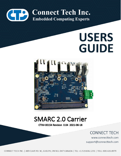
SMARC 2.0 Carrier CTIM-00154 Revision 0.04 2021-06-18TABLE OF CONTENTSTable of Contents (2)Preface (3)Disclaimer (3)Customer Support Overview (3)Contact Information (3)Limited Product Warranty (4)Copyright Notice (4)Trademark Acknowledgment (4)ESD Warning (5)Revision History (5)Introduction (6)Product Features and Specifications (6)Part Numbers / Ordering Information (6)Product Overview (7)Block Diagram (7)Connector Summary & Locations (8)Figure 1 Top view (8)Figure 2 Bottom view (8)Jumper/Switch Summary & Locations (9)Detailed Feature Description (10)SMARC 2.0 Connector (10)Fan Connector (11)Video Output (11)MIPI CSI Video Input (12)MIPI CSI x4/x2 Connector (12)MIPI CSI x2 Connector (13)Network (14)USB (14)Mini-PCIe/mSATA Slots (15)Carrier Control DIP Switch (17)HDMI0 DDC Level Translation Select Jumper (17)I2C Connector (18)RS-232 Serial Connector (18)microSD Card Slot (19)GPIO Connector (19)Power Input (20)External RTC Input (20)System Control Connector (21)Typical Installation (22)Cables (22)PREFACEDisclaimerThe information contained within this user’s guide, including but not limited to any product specification, is subject to change without notice.Connect Tech assumes no liability for any damages incurred directly or indirectly from any technical or typographical errors or omissions contained herein or for discrepancies between the product and the user’s guide.Customer Support OverviewIf you experience difficulties after reading the manual and/or using the product, contact the Connect Tech reseller from which you purchased the product. In most cases the reseller can help you with product installation and difficulties.In the event that the reseller is unable to resolve your problem, our highly qualified support staff can assist you. Our support section is available 24 hours a day, 7 days a week on our website at:/support/resource-center/. See the contact information section below for more information on how to contact us directly. Our technical support is always free.Contact InformationLimited Product WarrantyConnect Tech Inc. provides a two-year Warranty for this product. Should this product, in Connect Tech Inc.'s opinion, fail to be in good working order during the warranty period, Connect Tech Inc. will, at its option, repair or replace this product at no charge, provided that the product has not been subjected to abuse, misuse, accident, disaster or non-Connect Tech Inc. authorized modification or repair.You may obtain warranty service by delivering this product to an authorized Connect Tech Inc. business partner or to Connect Tech Inc. along with proof of purchase. Product returned to Connect Tech Inc. must be pre-authorized by Connect Tech Inc. with an RMA (Return Material Authorization) number marked on the outside of the package and sent prepaid, insured and packaged for safe shipment. Connect Tech Inc. will return this product by prepaid ground shipment service.The Connect Tech Inc. Limited Warranty is only valid over the serviceable life of the product. This is defined as the period during which all components are available. Should the product prove to be irreparable, Connect Tech Inc. reserves the right to substitute an equivalent product if available or to retract the Warranty if no replacement is available.The above warranty is the only warranty authorized by Connect Tech Inc. Under no circumstances will Connect Tech Inc. be liable in any way for any damages, including any lost profits, lost savings or other incidental or consequential damages arising out of the use of, or inability to use, such product.Copyright NoticeThe information contained in this document is subject to change without notice. Connect Tech Inc. shall not be liable for errors contained herein or for incidental consequential damages in connection with the furnishing, performance, or use of this material. This document contains proprietary information that is protected by copyright. All rights are reserved. No part of this document may be photocopied, reproduced, or translated to another language without the prior written consent of Connect Tech, Inc. Copyright © 2021 by Connect Tech, Inc.Trademark AcknowledgmentConnect Tech, Inc. acknowledges all trademarks, registered trademarks and/or copyrights referred to in this document as the property of their respective owners. Not listing all possible trademarks or copyright acknowledgments does not constitute a lack of acknowledgment to the rightful owners of the trademarks and copyrights mentioned in this document.ESD WarningElectroStatic Discharge (ESD). When handling anycircuit board assemblies including Connect TechCOM Express carrier assemblies, it is recommendedthat ESD safety precautions be observed. ESD safebest practices include, but are not limited to:•Leaving circuit boards in their antistaticpackaging until they are ready to be installed.•Using a grounded wrist strap when handlingcircuit boards, at a minimum you should touch agrounded metal object to dissipate any staticcharge that may be present on you.•Only handling circuit boards in ESD safe areas,which may include ESD floor and table mats,wrist strap stations and ESD safe lab coats.•Avoiding handling circuit boards in carpetedareas.•Try to handle the board by the edges, avoidingcontact with components.REVISION HISTORYINTRODUCTIONConnect Tech’s SMARC 2.0 carrier is an extremely small SMARC carrier board ideal for low power IoT applications as users can take advantage of the integrated on-board wireless capabilities found on the SMARC 2.0 modules. The carrier has USB 3.0, USB 2.0, 2x MIPI CSI-2 camera interfaces, HDMI outputs, microSD, and expansion via two mini PCIe Full size slots.Connect Tech’s SMARC 2.0 carrier board supports the latest generation Apollo Lake x86 low-powered processors and exposes next-generation interconnect (USB 3.0, DDI, MIPI-CSI-2).SMARC 2.0 supports an extended temperature range of -40°C to +85°C and offers a very small footprint; ideal for mobile or stationary applications.Product Features and SpecificationsPart Numbers / Ordering InformationPRODUCT OVERVIEW Block DiagramConnector Summary & LocationsFigure 1 Top viewFigure 2 Bottom viewJumper/Switch Summary & LocationsDETAILED FEATURE DESCRIPTIONSMARC 2.0 ConnectorThe processor and chipset are implemented on the SMARC 2.0 Module, which connects to the SMARC 2.0 Carrier via an MXM 3.0 fine pitch connector.Fan ConnectorThe SMARC 2.0 Carrier implements a 4 pin header for the connection of a +5V fan. No PWM control is available from this header.Video OutputThe SMARC 2.0 Carrier implements two HDMI outputs. Both ports are from the SMARC 2.0 module. All connectors are industry standard HDMI Type A upright right angle.MIPI CSI Video InputThe SMARC 2.0 Carrier implements two MIPI CSI camera inputs through 28 pin Hirose ZIF connectors compatible with Basler BCON cables. The pinout of this connector is compatible with Basler MIPI BCON *********************************************************************************. MIPI CSI x4/x2 ConnectorMIPI CSI x2 ConnectorNetworkThe SMARC 2.0 Carrier implements two 10/100/1000 Ethernet interfaces.USBThe SMARC 2.0 Carrier implements a Dual USB3.0 connector and a Dual USB2.0 connector. All ports are direct from the SMARC 2.0 module. All connectors are industry standard USB3.0/USB2.0 Type A right angle.Mini-PCIe/mSATA SlotsThe SMARC 2.0 Carrier implements two expansion slots. One is Mini PCIe only and the other is a dual function Mini PCIe/mSATA socket.The dual purpose functional Mini-PCIe/mSATA socket located at P8 can accept either a Mini PCIe module or an mSATA module. The slot has circuitry that allows for the selection between connecting PCIe lanes or SATA lanes to the connector. This slot also contains a USB 2.0 link as per the Mini PCIe specification.Carrier Control DIP SwitchHDMI0 DDC Level Translation Select JumperSome SMARC module manufacturers do not use 1.8V signal levels for the HDMI DDC interface, for the best and most reliable performance it is required the correct voltage level is used.Note that prolonged use at the incorrect voltage level may cause damage. If you are unsure what logic *****************************************************************************. Customers using the Congatec conga-SA5 will need to set this jumper to 3.3V (position 1-2).I2C ConnectorThe SMARC 2.0 Carrier implements a 3 pin header that connects to the I2C interface from the SMARC 2.0 module.RS-232 Serial ConnectorThe SMARC 2.0 Carrier implements a 9 pin header that connects to the UART0 interface via an RS232 transceiver from the SMARC 2.0 module.microSD Card SlotThe SMARC 2.0 Carrier implements a microSD card connector.GPIO ConnectorThe SMARC 2.0 Carrier implements a 10 pin header that connects to a MaxLinear XRA1200 I2C GPIO expander at address 0x40.Power InputThe SMARC 2.0 Carrier accepts a single power input to power all onboard devices.A single +5V DC (± 5%) input is required for operation.External RTC InputThe SMARC 2.0 Carrier has an optional external RTC input header.System Control ConnectorThe SMARC 2.0 Carrier implements a 10 pin header that connects to several system control signals from the SMARC module.TYPICAL INSTALLATION1.Ensure all external system power supplies are off.2.Install the SMARC module into the MXM connector. Be sure to follow the manufacturer’s directionfor proper heatsink/heat spreader installation and any other cooling instructions from themanufacturer.3.Install the necessary cables for the application. For the relevant cables, see the Cables andAccessories section of this manual.4.Connect the power cable to the SMARC 2.0 Carrier then to the power supply.5.Switch on the power supply. DO NOT power up your SMARC system by plugging in live power. CABLES*******************************************************************************.。
FITEL S179手持核对融接设备说明书

Features and Benefits • Fast and consistent fiber splicing for exceptional performance • NEW design features enhanced ease of use, maintenance, speed and shock resistance (see page 2)• Large capacity, internal battery charging system allows 200 splicing cycles (splicing/heating) in one charge 1Overview The powerful FITEL S179 Hand-Held, Core Alignment Fusion Splicer delivers fast and reliable optical fiber splicing even under harsh environmental conditions. Offering a wide range of capabilities, this fusion splicing machine opens the door to an entirely new range of applications. Product Description Designed with end users and rugged field use in mind, the FITEL S179 Fusion Splicer delivers rapid splicing and heating for consistent results, splice after splice. Suitable for use with ultra-bend insensitive and large area effective fibers, this fusion splicing machine is an excellent choice for a variety of deployments including data centers, Metro and FTTx.A broad range of new features that enhance communication, ease of use, portability and field durability combine to make the S179 Fusion Splicer one of the most powerful and user-friendly fusion splicing machines available today.1 In semi-auto splicing mode and regular heating mode • Wide splicing chamber for easy fiber loading • Lower profile, lighter weight design enhances portability • Powerful, high-propulsion motor (8N) for stable splicing • Compatible with Splice-On-Connectors (SOC)Applications• Fiber sensors• Manufacture of opticalcomponents• FTTx• LAN• Backbone• Enterprise• Long-haul• Data CentersAuthorized Distributor of FITEL Productsin the Americas ®2 | NEW FeaturesUnder Tough Environments2 IK07 rating Mechanical Impact means that the machine protects against 2 jour impact, it is equivalent to 500g force from 40cm. This rating does not guarantee that the machine will always be undamaged under these conditions.3 Standard operations could be carried out after conducting the above tests. These tests were performed at the Furukawa Electric Co., Ltd. laboratories with no significant damage resulting. This result does not guarantee that the machine will always be undamaged under these conditions.4 IPX2 rating drip proof means that the machine can be exposed to 3 mm/min drips for 10 minutes with 15 degree tilt and still function.5 IP5X rating dust proof means that the machine can be exposed to dust particles with a diameter of 0.1 µm to 25 µm and still function.• Shock Resistant: Equivalent to IK07 rating Mechanical impact2• Drop Resistant: 76 cm drop tests from 5 different angles3120 cm drop tests with hard carrying case3• Water Resistant: Equivalent to IPX2 rating drip proof4• Dust Resistant: Equivalent to IP5X rating dust proof5• Touch Screen: 4.3-inch wide LCD screen with touch panel for easy, intuitive operation• Illumination Lamp: 3 upper + 1 lower LED lights illuminate the entire splicing chamber• Detachable V-Groove: Easy maintenance and lens cleaning• Near Field Communication (NFC): Lock and unlock splicer via smartphone (only for Android phones, ver. 4.1 or later)• Wi-Fi Networking: Communication between splicer and smartphone• High Speed:6 seconds of splicing time and 9 seconds of heating timeDUST RESISTANT SHOCK RESISTANT WATER RESISTANTDROP RESISTANTNFC:LOCK AND UNLOCK ILLUMINATION LAMP:3+ 1 LED LIGHTSDETACHABLE V-GROOVEFOR EASY CLEANINGFITEL® S179 Fusion SplicerApplicable Fibers SM (ITU-T G.652, G.657A1 and G.657A2), MM (ITU-T G.651), DSF (ITU-T G.653), Cut-off Shifted Fiber (ITU-T G.654, Large Area type), NZD (ITU-T G.655), BIF/UBIF (Bend Insensitive Fiber ITU-T G.657B3)Cladding Diameter80 - 150 μmCoating Diameter100 - 3000 μmFiber Cleave Length 5 - 16 mmAverage Splice Loss SM:0.02 dB, MM:0.01 dB, DSF:0.04 dB, NZD:0.04 dB Splice Time 6 seconds (Semi-auto mode) 9 seconds (Regular mode)Heat Time6 9 (60 mm, Tyco SMOUV1120-01, coating diameter 250-900 µm, Power mode) 13 (60 mm, FITEL S921, coating diameter 250 µm, Power mode)15 (60 mm, FITEL S921, coating diameter 900 µm, Power mode)Splice Programs Max. 300Automatic Splicing Selection AvailableHeat Programs Max. 100Automatic Heating Start AvailableApplicable Sleeves20/40/60 mmFiber Holder Tight Holder (loose tube applicable) or Removable Fiber Holder SystemTension Test 1.96 NSplice Return Loss70 dB or moreAttenuation Splice Function Intentional high splice loss of 0.1 dB to 15 dB (0.1 dB step) can be made for an inline fixed attenuator Fiber Image Magnification104X, 278X, 556XSplice Result Storage20,000Image Capture Capacity Last 100 images to be automatically captured + up to 100 images to be stored permanentlyDimension 139 W x 209 D x 114 H mm (not including shock absorber) 179 W x 246 D x 131 H mm (including shock absorber)Weight 1.7 kg (without battery), 2.0 kg (with battery)Monitor 4.3-inch wide color LCD monitor with touch screenPropulsion (motor)8 N (designed value)Data Output USB ver. 2.0 mini B x 1 port, Standard A x 1 portBattery Capacity7Typical 200 splice/heat cycles, 90 second/cycleAltitude5000 mWind Protection15 m/sOperating Temperature-10 to + 50 °C (without excessive humidity)Storage Temperature-40 to +60 °C (without excessive humidity)Humidity0% to + 95% RH (non-condensing)Power Source AC Input 100 to 240 V (50/60Hz), DC Input 11 to 24 V6 The heating time may vary depending on the type of sleeve. In addition, the first heating time after turning the power on can be longer than the standard heating time.7 The number of splicing and heating cycles the machine can perform with a fully charged battery at 20 ̊C in semi-auto splicing mode and regular heating mode. The number of cycles may vary depending on the battery status and operating conditionsS179 Fusion Splicer | 3For additional information please contact your sales representative.You can also visit our website at or call 1-888-fiberhelp (1-888-342-3743) USA or 1-770-798-5555 outside the USA.Fusion Splicer Customer Service,Training and Service Center Toll Free: 866-452-9516Phone: 678-783-1090Fax: 678-783-1093Email:**********************OFS Corporate Headquarters 2000 Northeast ExpresswayNorcross, Georgia 30071, USAOrdering Information Code Description S179A-21S179A splicer with 10mm Fiber Holder S712T-010S179A-31S179A splicer without any Fiber Holders S179A-EX-10S179A splicer with S712T-010 holder, S211B stripper, cleaver, wipes and fluid S179A-EX-900S179A splicer with S712S-250 and S712S-900 holder, S211B stripper, cleaver, wipes and fluid Standard Package Item P/N Quantity FITEL S179 Fusion Splicer S179A 1Built-in Battery Pack S947A 1Hard Carrying Case HCC-051Spare Electrodes ELR-011AC Adapter S979A 1AC Power Cord -1Cooling Tray CTX-031Cleaning Brush VGC-011Electrode Sharpener D51111Tool Case TCC-011LCD anti-reflective sheet ARS-011Instruction Manual UMC-021Quick Reference Guide FTS-B5261Optional Components Item P/N Quantity USB Cable USB-011Battery Charger S980A 1Soft Carrying Case SCC-011Angled Stand AGS-021Working Belt WBT-011Car Cigarette Cable CDC-041Heater Clamp Base for SOC HBS-011Tight Holder 16 mm Cleave Length 10 mm Cleave Length Universal S712-T-016 S712T-010 S712T-UN 1 pair 1 pair 1 pair Fiber Holder 160 µm coated fiber S712S-160 1 pair 250 µm coated fiber S712S-250 1 pair 500 µm coated fiber S712S-500 1 pair 900 µm coated fiber S712S-900 1 pair Fiber Holder Loose Tube Fiber (Left side)S712S-LT-L 1 pair Loose Tube Fiber (Right side)S712S-LT-R 1 pair SOC Holder S712C-SGS9-L 1 Seiko Giken FC/SC ferrule (9 mm)S712C-SGS5-L 1 Seiko Giken FC/SC ferrule (5 mm)S712C-SGL9-L 1 Seiko Giken LC ferrule (9 mm)S712C-SGL5-L 1 Seiko Giken LC ferrule (5 mm)S712C-DM25-L 1 Seiko Giken TOUCH Plus SC (9 mm)S712C-SGC5-R 1 Diamond E2000TM /E3000TM ferrule S712C-SGC9-R 1 Seiko Giken Cordage (5 mm)S712C-DMC5-R 1 Seiko Giken Cordage (9 mm)S712C-SGC9-R 1 Diamond Cordage (5 mm)S712C-DMC5-R 1 Wi-Fi dongle WFD-011AccessoriesStandard Package。
SBL-902C拼接板规格书V1.2
48.363 56.476 58.200 60.023 47.776 60.289 60.680 79.976 47.720 55.469 64.674 76.600
60.004 70.069 72.000 75.029 59.870 74.893 57.030 75.025 59.799 59.901 59.883 59.883
2
版本号 1.1 1.2
版本变更记录
日期
页码
2014-12-20
2014-02-04
内容 第一版发行 第二版发行
3
1、 产品概述
SBL-902C 是我司最新设计的拼接液晶驱动板,该液晶图像处理板采 用了运动侦测与补偿运算、内插运算、边缘平滑处理及杂波信号抑制等尖端 处理技术,其 3D 视频亮色分离电路单元, 3D 的逐行处理及帧频归一转化电 路单元, 3D 数字信号降噪单元,可将普通 PAL/NTSC 隔行扫描视频信号采集 变为逐行扫描的,还原高画质、高分辨率的高清信号和计算机图像信号。
------LVDS ODD 0 - Signal LVDS ODD 0 + Signal LVDS ODD 1 - Signal LVDS ODD 1 + Signal LVDS ODD 2 - Signal LVDS ODD 2 + Signal ----LVDS ODD Clock - Signal
键 LEFT RIGHT 备用
CN14 和 CN20 (10pin/2.54) 背光供电电源插座
1
+24V
Power
2
+24V
Power
3
+24V
Power
4
+24V
阿尔普山盾 SKHC 系列 - 基本信息说明书
|Dimensions |Mounting Hole Dimensions |Circuit Diagram |Packing Specifications |Soldering Conditions Snap-in Type TACT Switch™ > SKHC Series > SKHCBKA01012mm Square Type (Snap-in) SKHC Series||TypeSnap-in Operating force0.74N Operating directionTop push Travel0.3mm Operating life(5mA 5V DC)500,000 cyclesInitial contact resistance 100mΩ max.Stem colorBlue StemFlat stem Series type Sharp feeling typePart number Series Common InfoSKHCBKA010Operating temperaturerange-40℃ to +85℃Rating (max.)50mA 12V DC Rating (min.)10µA 1V DCElectrical performance Insulationresistance100MΩ min. 100V DC for 1min. Voltageproof250V AC for 1 min.Durability Vibration 10 to 55 to 10Hz/min., the amplitude is 1.5mm for all the frequencies, in the 3 direction of X, Y and Z for 2 hours respectivelyEnvironmental performance Cold-40±2℃ for 96hDry heat90±2℃ for 96hDampheat60±2℃, 90 to 95%RH for 96hMinimum order unit (pcs.)Japan1,000 Export1,000DimensionsMounting Hole DimensionsViewed from mounting face.Circuit DiagramPacking Specifications BulkNumber of packages (pcs.)1 case / Japan5,0001 case / export packing15,000Export package measurements (mm)309×476×347Soldering ConditionsConditions for Auto-dipItems ConditionFlux built-up Mounting surface should not be exposed to fluxPreheating temperature Ambient temperature of the soldered surface of PC board. 100℃ max.Preheating time60s max. Soldering temperature260℃ max. Duration of immersion5s max. Number of soldering 2 times max.Manual SolderingItems Condition Soldering temperature350℃ max.Duration of soldering3s max.Capacity of soldering iron60W max.1. Do not washing the TACT Switch™.2. Prevent flux penetration from the top side of the TACT switch™.3. Switch terminals and a PC board should not be coated with flux prior to soldering.4. The second soldering should be done after the switch returns to normal temperature.5. Use the flux with a specific gravity of at least 0.81.(EC-19s-8 by TAMURA Corporation, or their equivalents.)Notes are common to this series/models.1. This site catalog shows only outline specifications. When using the products, pleaseobtain formal specifications for supply.2. Please use 1.6mm thick PC boards.3. Please place purchase orders per minimum order unit (integer).4. Please contact us for automotive use products.Inquiries about ProductsInquiryCOPYRIGHT© 2020 ALPS ALPINE CO., LTD。
PTX-LCD系列激励器说明书

3
音频输入 音频母板 立体声/ 单声道板 PLL/VCO
CPU 板板
功放
图 4-2 激励器俯视图
1.4 激励器原理框图
激励器连线框图如图 4-3 所示:
音频接口板
编码板或 单声/MPX板
音频输入板 音频母板
电源板板 变压器 开关电源
散热器 显示面板卡
VCO板 PLL板
(3) 选件清单如表 4-3 所示。(机器的标准配置不包括选件,如用户需要请
另行购置。)
/03 /08 /AUDIOINP-DIG
表 4-3 24V外电源SP 技术的数/模音频接口,集成数字 立体声编码器及 RDS 编码器
(4) 数字音频输入接口(AUDIOINP-DIG)指标如表 4-4 所示。
PTX-LCD激励器严格按照模块化方法设计:不同功能由不同模块完成,各模 块直接相接(某一模块的凸性接口与另一模块的凹性接口接插)或由连接器终端 电缆相连。这种设计理念使得单一模块的维修和替换变得非常简单。
1.2 激励器外观图
激励器外观图如图 4-1 所示。
图 4-1 激励器外观图
1.3 激励器内部布局
(5) 基于 DSP 技术的数/模音频接口(TRDSP)指标如表 4-5 所示。
模拟音频输入 A/D 转换 连接器 阻抗 输入电平 最大输入电平 数字音频输入 连接器 数据格式 采样率 数字音频输出 连接器 数据格式 采样率 MPX 输出 D/A 转换 导频频率 导频电平 导频相位 38kHz 副载波抑制度 MPX 输出电平 立体声分离度 MPX 输出噪声 预加重 预加重线性度 15kHz 低通滤波器频响 19kHz 处衰减 限幅斩波 AGC
>82dB(RMS,50us 预加重,75kHz 频偏) ±0.05dB (20kHz ~ 53kHz) ±0.2dB (53kHz ~ 100kHz) <0.02% <0.02% (1K+1.3K,1:1,75kHz 频偏) >50dB(典型值 60dB)
霍尼韦尔+MLX90109+评估板+说明书
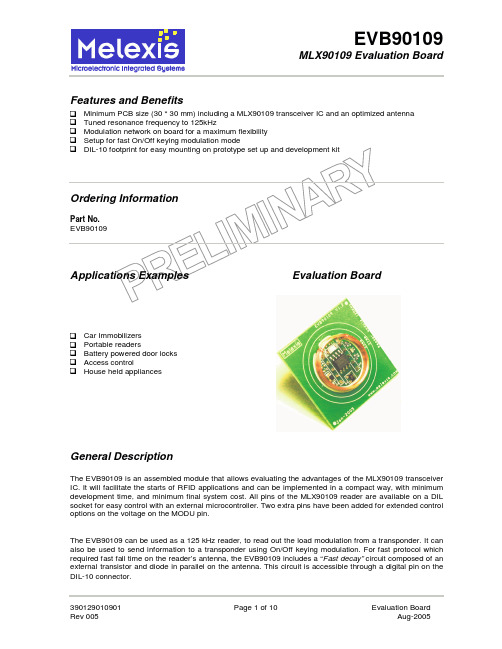
Features and BenefitsMinimum PCB size (30 * 30 mm) including a MLX90109 transceiver IC and an optimized antennaTuned resonance frequency to 125kHzModulation network on board for a maximum flexibilitySetup for fast On/Off keying modulation modeCar ImmobilizersPortable readersBattery powered door locksAccess controlHouse held appliancesGeneral DescriptionThe EVB90109 is an assembled module that allows evaluating the advantages of the MLX90109 transceiver IC. It will facilitate the starts of RFID applications and can be implemented in a compact way, with minimum development time, and minimum final system cost. All pins of the MLX90109 reader are available on a DIL socket for easy control with an external microcontroller. Two extra pins have been added for extended control options on the voltage on the MODU pin.The EVB90109 can be used as a 125 kHz reader, to read out the load modulation from a transponder. It can also be used to send information to a transponder using On/Off keying modulation. For fast protocol which required fast fall time on the reader’s antenna, the EVB90109 includes a “Fast decay” circuit composed of an external transistor and diode in parallel on the antenna. This circuit is accessible through a digital pin on the DIL-10 connector.Table of Contents1 EVB90109 ELECTRICAL SPECIFICATIONS (3)2 DESCRIPTION (3)2.1G ENERAL EXPLANATION (3)2.2P ARALLEL ANTENNA (4)2.3M ODULATION NETWORK (4)2.4A NTENNA VOLTAGE IN READ OPERATION (4)2.5N OISE CANCELLATION IN READ OPERATION (5)2.6A NTENNA VOLTAGE IN 100% MODULATION OPERATION (5)2.7F AST DECAY CIRCUIT (6)3 SCHEMATIC (7)4 PHYSICAL OUTLINE (8)5 PINNING OF THE EVB90109 (9)6 COMPONENTS (9)7 DISCLAIMER (10)1 EVB90109 Electrical Specificationsreduce the fall time of the antenna. For more information, please refer to the application note “100% Modulation (On/Off keying)”. An additional footprint of “Modulation network” is available on the board and is accessible through the MODUR3 digital connection. All others digital connections as SPEED, MODE, MODU, CLOCK and DATA, are available on the DIL-10 connector.Figure 1: EVB90109Note: The EVB90109 does not include any pull-up resistors on the digital connections DATA and CLOCK. This must be done externally, by configuring the IO ports of a microcontroller in pull-up mode, or by adding two external resistors connected between the digital pins and Vdd.Parallel resonant antenna (L, C4, C5) Fast decay circuit (Q1, MLX90109Modulation Network (R1, R2)Connector DIL-102.2 Parallel antennaThe parallel antenna of the EVB90109 consists of the inductance (L) based on the MLX90125 reader coil and the tune capacitor (C4), which form a resonant system at 125 kHz with a total (inductance and capacitance) antenna impedance of about 1.3kOhms. The MLX90109 is specified to drive a minimal antennabe smaller margin in theof the antenna to work with a high quality factor and then to get the maximum of operating distance.2.3 Modulation networkThe modulation network is used to set the voltage on the MODU pin of the MLX90109. As shown in the following formula, the voltage on the antenna can be adjusted according to this voltage. This features can be used to reduce the power consumption of the chip by setting a lower voltage on the antenna. Under no circumstances it can be used to make proportionnal modulaiton, due to internal feedback loop which doesn’t allow this use.overshoot MODU DD ant V V V V −−=The EVB90109 is provided with two resistors R1 and R2 as the modulation netwok controlled through the pin MODUR2 to set the voltage on the antenna respectively On (Vmodu to 0.8 Volts) and Off (Vmodu to 5 Volts). Others footprint C1, C3 and R3 and an extra pin MODUR3 are available on the board and can be used for specific applications.2.4 Antenna voltage in read operationThe resistors R1 and R2 set VMODU to 0.8V (1V for full temperature range [–40, 85] C) which is the lowest possible voltage to guarantee that the antenna driver of the MLX90109 stays out of its linear operating zone. The field is set On (VMODU to 0.8V) and Off (VMODU to VDD) when applying 0V and VDD on pin MODUR2.2.5 Noise cancellation in read operationThe resonant antenna is a natural band-pass filter, which becomes more effective as Q ant increases.The MLX90109 has an internal first order filtering of the envelope that changes according to the setting of the SPEED pin to fit to the biphase and Manchester data spectrum:Note:mode.The modulation network R1 and R2 can be used to set the voltage amplitude on the antenna On and Off by applying 0 Volts and Vdd on the pin MODUR2.Switching ON the magnetic field depends on the internal driver of MLX90109 and takes less than 5 carrier periods. Switching OFF the magnetic field depend on the quality factor (Qant) of the parallel antenna connected to the reader (about 24 periods with the EVB90109). To reduce this fall time, the “fast decay” circuit can be used.2.7 Fast decay circuitVery small fall time may be required in fast protocol, to be understood by the transponder in the field. This is why, the EVB90109 include a “fast decay” circuit controlled through the pin FAST_DECAY and composed of the transitstor Q1 and the diode D1. The following picture shows how to implement the “fast decay” system.Picture 1: Fast Decay module control, (1) Antenna, (2) MODUR2, (3) FAST_DECAY3 SchematicThe following diagram shows the schematic of the EVB90109. All components in grey are not mounted but the footprints are present if the user wants to use it for dedicated applications.Figure 2: Schematic of the EVB901094 Physical outlineThe following figure shows the outline of the MLX90109 evaluation board.Figure 3: EVB90109 outline: top sideR2C1R1R3C3D1C4Q1MLX90109CoilDIL-10DIL-101 2 34 51098 7 65 Pinning of the EVB90109Table 3: Components7 DisclaimerDevices sold by Melexis are covered by the warranty and patent indemnification provisions appearing in its Term of Sale. Melexis makes no warranty, express, statutory, implied, or by description regarding the information set forth herein or regarding the freedom of the described devices from patent infringement. Melexis reserves the right to change specifications and prices at any time and without notice. Therefore, prior to designing this product into a system, it is necessary to check with Melexis for current information. This product is intended for use in normal commercial applications. Applications requiring extended temperature range, unusual environmental requirements, or high reliability applications, such as military, medical life-support or life-sustaining equipment are specifically not recommended without additional processing by Melexis for each application.The information furnished by Melexis is believed to be correct and accurate. However, Melexis shall not be liable to recipient or any third party for any damages, including but not limited to personal injury, property damage, loss of profits, loss of use, interrupt of business or indirect, special incidental or consequential damages, of any kind, in connection with or arising out of the furnishing, performance or use of the technical data herein. No obligation or liability to recipient or any third party shall arise or flow out of Melexis’ rendering of technical or other services.© 2005 Melexis NV. All rights reserved.For the latest version of this document, go to our website atOr for additional information contact Melexis Direct:Europe and Japan: All other locations:Phone: +32 1367 0495 Phone: +1 603 223 2362E-mail:************************E-mail:*********************ISO/TS 16949 and ISO14001 Certified。
xl9021 演示板手册说明书

页数:第1 页,共4 页描述XL9021提供的演示板,用于DC5V~36V输入,输出电流2.5A的降压恒压应用演示,最高转换效率可以达到95%。
XL9021是同步整流降压型DC-DC转换芯片,固定开关频率150KHz,可减小外部元器件尺寸,方便EMC设计。
芯片具有出色的线性调整率与负载调整率,输出电压支持1.25V~25V间任意调节。
芯片内部集成短路保护、过流保护、过温保护等可靠性模块。
XL9021为标准SOP8封装,集成度高,外围器件少,应用灵活。
DEMO原理图引脚介绍物料清单页数:第2 页,共4 页DEMO实物图实物图正面实物图反面PCB布局PCB顶层截图PCB底层截图页 数:第 3 页, 共 4 页典型性能参数E f f i c i e n c y (%)Output current(A)O u t p u t v o l t a g e (V )Output current(A)5.0V 输出效率曲线 5.0V 输出线性调整率与负载调整率曲线瞬态负载响应波形瞬态负载响应波形(VIN=12V ,VOUT=5.0V ,IOUT=0.1至1A ) (VIN=24V ,VOUT=5.0V ,IOUT=0.1至1A )EN 引脚开关机波形 EN 引脚开关机波形(VIN=12V ,VOUT=5.0V ,IOUT=0.5A ) (VIN=24V ,VOUT=5.0V ,IOUT=0.5A )页数:第4 页,共4 页应用信息输入电容选择在连续模式中,转换器的输入电流是一组占空比约为VOUT/VIN的方波。
为了防止大的瞬态电压,必须采用针对最大RMS电流要求而选择低ESR(等效串联电阻)输入电容器。
对于大多数的应用,1个100uF的输入电容器就足够了,它的放置位置尽可能靠近XL9021的位置上。
最大RMS电容器电流由下式给出:IRMS≈IMAX*√VOUT(VIN-VOUT)VIN其中,最大平均输出电流IMAX等于峰值电流与1/2 峰值纹波电流之差,即IMAX=ILIM-△IL/2。
GCE-2001全国产化说明书

说明除列明随产品配置的配件外,本手册包含的内容并不代表本公司的承诺,本公司保留对此手册更改的权利,且不另行通知。
对于任何因安装、使用不当而导致的直接、间接、有意或无意的损坏及隐患概不负责。
订购产品前,请向经销商详细了解产品性能是否符合您的需求。
本手册所涉及到的其他商标,其所有权为相应的产品厂家所拥有。
本手册内容受版权保护,版权所有。
未经许可,不得以机械的、电子的或其它任何方式进行复制。
温馨提示1、产品使用前,务必请仔细阅读产品说明书。
2、对未准备安装的主板,应将其保存在防静电保护袋中。
3、在从包装袋中拿主板前,应将手先置于接地金属物体上一会儿,以释放身体及手中的静电4、在使用前,宜将主板置于稳固的平面上。
5、请保持主板的干燥,散热片的开口缝槽是用于通风,避免机箱内的部件过热。
请勿将此类开口掩盖或堵塞。
6、在将主板与电源连接前,请确认电源电压值。
7、请将电源线置于不会被践踏的地方,且不要在电源线上堆置任何物件。
8、当您需连接或拔除任何设备前,须确定所有的电源线事先已被拔掉。
9、为避免人体被电击或产品被损坏,在每次对整机、板卡进行拔插或重新配置时,须先关闭交流电源或将交流电源线从电源插座中拔掉。
10、请留意手册上提到的所有注意和警告事项。
11、为避免频繁开关机对产品造成不必要的损伤,关机后,应至少等待30秒后再开机。
12、设备在使用过程中出现异常情况,请找专业人员处理。
13、请不要将本设备置于或保存在环境温度高于70℃上,否则会对设备造成伤害。
目录1.产品简介 (1)1.1概述 (1)1.2产品特点 (2)1.3产品优势 (2)1.4技术指标 (3)2.细参数说明 (4)2.1产品图片 (4)2.2 测试套板接口图片 (5)2.3 COMe外形尺寸 (6)2.4 COMe连接器接口定义 (7)1.产品简介1.1概述随着具备高性能计算能力的智能装备在诸如:工业、农业、能源、国防、医疗、交通、民生等多个领域的推广和应用,越来越多的企业将大量资源,投入到高性能计算能力的智能装备的研发和生产中。
icmef052p120nfr规格书
ICMEF052P120NFR是一款符合工业标准的高性能的SMT表面组装模块,其规格书如下:型号:ICMEF052P120NFR尺寸:长x宽x高=12.5mm x 12.5mm x 0.6mm材料:陶瓷工作温度范围:标准规格为-40℃至+85℃,但根据应用和设计,温度范围可能有所不同电气性能:* 引脚间距:0.65mm,符合QFN封装标准* 工作电压:1.8V至3.6V,具体取决于应用需求* 逻辑状态:高电平=0V,低电平=VCC-1.5V* 功耗:低于30mA功能特性:* 具有开关和放大功能,可用于多种传感器和执行器应用* 内置补偿电路,提高线性度和抗干扰能力* 具有反向极性保护功能,适用于不同方向连接的组件* 工作频率:在特定的电压范围内,工作频率是稳定的* 工作环境要求:芯片工作温度范围、供电电压和电流等参数会影响性能和稳定性封装:塑料底部连接器(QFN)封装,这种封装形式具有低成本、高可靠性和易于组装的特点,适合于SMT表面组装技术包装:常规包装为每卷500个元件,也可根据客户需求提供其他包装方式注意事项:* 在使用前,请务必检查元件温度范围、工作电压和其他规格是否符合您的应用需求* 在组装过程中,请确保正确的安装方式和适当的固定方式,以避免不必要的损坏* 请遵循正确的操作步骤和工艺要求,以确保元件的稳定性和可靠性* 如需进一步了解该元件的详细信息,请参考相关技术资料和手册总的来说,ICMEF052P120NFR是一款功能强大、性能稳定的SMT表面组装模块,适用于各种传感器和执行器应用。
其低成本、高可靠性和易于组装的特性使其成为一种极具竞争力的解决方案。
在选择和使用此元件时,请务必遵守相关的操作指南和规范,以确保其稳定的工作和长期的可靠性。
YJX-C58A-微型热敏打印机芯规格书v1.3

V V 驱动输出部
分,参考值
3.7 、时序特性(25±10℃)
参数
代号
表7
速度
单位
最小 典型 最大
时钟频率
-- -fCLK
-- --
时钟宽度
twCLK 30 --
数据建立时间 testup DI 30 --
数据保持时间 thold DI 30 --
8 MHz
5 MHz -- ns -- ns -- ns
组成,使传动噪声极低。
-3-
2、 规格参数
项目 打印方法 有效打印宽度(毫米) 点密度(点/毫米) 打印点数 纸张宽度(毫米) 点间距(毫米) 点大小 最大打印速度 走纸精度 打印头温度侦测 缺纸侦测 打印头工作电压(DCV) 逻辑工作电压(DCV) 电机工作电压(DCV) 工作温度 工作湿度 储藏温度 储藏湿度 机械噪音 胶辊开合次数 对热敏纸牵引力 对热敏纸抓握制动力
步距角
9º(1-2 相激励)
步进距离
0.0625 毫米
相电阻
10 Ω±7%
20℃
相电流
0.357 A
驱动方式
双极,双相驱动(或 1~2 相)
4.2、步进电机相位
CA58 的步进电机采用 1-2 相驱动方 式,有 4 个位置。如下表所示:
表 10
位置
A B
A
STEP1
+ -
-
STEP2
-
-
STEP3
-
25℃
热敏电阻的温度曲线图
图1
表 5 热敏电阻温度表:
温度 (℃) -20
阻值 KΩ) 269
温度 (℃)
10
阻值 (KΩ)
60
高科设备说明书
使用说明书
广 州 市 高 科 通 信 技 术 股 份 有 限 公 司
Guangzhou Gaoke Communications Technology Co.,LTD.
V2060-SE IP-PBX 使用说明书
版本: V2060SE-11-05-200
广州市高科通信技术股份有限公司热情为客户提供全方位的技术支持, 用户可与就近的高科办 事处联系,也可直接与公司客服部联系。
各类标志
本手册还采用各种醒目标志来表示在操作中应该特别注意的地方,这些标志意义如下:
注意: 提醒操作中应该注意的事项。
说明: 对操作内容的描述进行必要的补充和说明。
Байду номын сангаас
目录
前言.......................................................................................................................................................................4 1 2 概述...............................................................................................................................................................6 设备主要特性.............................................................................................................
WM013922R0102_WinControl_1800安装与指导手册

ABB PLC 介绍
AC500 可升级的可编程控制器 : 全新系列!当选择任何一种现场总线时,您的系统都将 是结构简单、可扩展性强、应用灵活的自动化系统。
S500 系列 I/O 模块
: 用于 AC500 系统的集中式和分布式扩展 I/O。
小型系统 AC31 40..50 系列 : 外观小巧但功能强大。有集中式和分布式扩展能力。
订货资料 .................................................................................................................. 2/22-26
外形尺寸图 .............................................................................................................. 2/27
2
技术数据 .................................................................................................................. 2/5-13
通讯功能 .................................................................................................................. 2/14-21
配方管理和监视列表
可显示所选变量的值,预置分配立即给要下载到控制系统的所有变量(“写配方”),系统 中运行的值可以通过读到监视列表和配方管理器中并保存在内存里(“读配方”),可在调 试时调用。这个功能在控制参数的整定时很有用。
电气连接器 SBLL-250 产品说明书
POWER-UTILITIESCATALOG NUMBERSBLL-250CERTIFICATIONSFEATURES镀锡铜模块可连接铜或铝导体可触及螺柱便于进行 nVent ERIFLEX Flexibar 或其他导体连接设计允许进行导体目视检查和连接确认可调整透明罩模块化插接结构用于组建多级分线盒可直接夹到 DIN 轨上或使用螺钉安装至面板直接面板安装需要 SBLEC 接线端子固定附件符合《电气、电子设备中限制使用某些有害物质指令》(RoHS) 标准无卤素产品属性Article Number: 561132Material: Copper;ThermoplasticFinish: 镀锡Max Current Rating, IEC: 290 AMax Current Rating, UL/CSA: 255 AShort Term Withstand Current (Icw) 1s: 14.4 kAPeak Short Circuit Current (Ipk): 42 kAShort Circuit Current Rating (SCCR): 100 kAMax Working Voltage, IEC (Ui): 1,000 VAC;1,500 VDCMax Working Voltage, UL (Vin): 1,000 VNumber of Stud Connections: 2Stud Connection Conductor Width: 20 – 24 mmStud Connection Compact Stranded Wire Size: 10 – 120 mm²Stud Connection Wire Size: #8 - 250 kcmilDepth: 65 mmHeight: 205.70 mmWidth: 52.300 mmA:108 mmUnit Weight: 0.160 kgCertification Details: UL® 1059Flammability Rating: UL® 94V-1Complies With: IEC® 60947-7-1ADDITIONAL PRODUCT DETAILS接线端子连接可互换,可用作线路端或负载端连接。
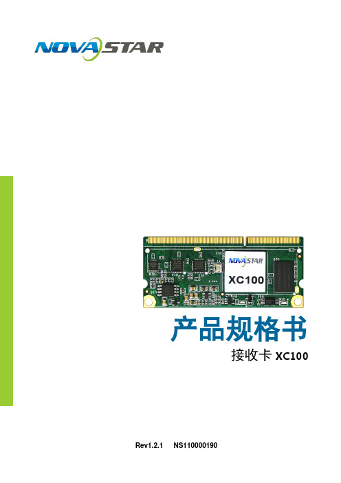
诺瓦科技LED显示屏接收卡XC100规格书
R1
33
34
R13
G1
35
36
G13
GND
37
38
GND
B1
39
40
B13
R2
41
42
R14
G2
43
44
G14
B2
45
46
B14
R3
47
48
R15
GND G3
49
50
GND
51
52
G15
司
B3 R4
53
54
B15
55
56
R16
公
G4
B4 GND R5 G5 B5 R6
57
58
G16
限 59
60
B16
能
A
17
18
HUB_CODE2
模
B
19
20
HUB_CODE3
组
C
21
22
HUB_CODE4
接
D
23
24
HUB_UART_RX
口
GND
25
26
GND
第4页
E
27
28
HUB_UART_TX
OE_RED
29
30
RFU3(OE_GREEN)
CTRL
31
32
RFU4(OE_BLUE)
91
92
B20
R9
93
94
R21
G9
95
96
G21
GND
97
98
GND
B9
99
100
TW9022规格书
推荐工作条件
符号 POUT1 POUT2 FOP 参数 输出功率(输入电压230V±15%) 输出功率(输入电压85V~265V) 系统工作频率 参数范围 <7 <5 <120 单位 W W KHz
电气参数(注4,
符号 VCC-CLAMP VCC-ON VCC-UVLO IST IOP VCS-TH VCS_SH ORT TLEB
5) (无特别说明情况下,VCC =15 V, TA =25℃) 描述 条件 最小值 典型值 电源电压 1mA VCC 上升 Vcc 下降 VCC=VCC-OM-1 FOP=70KHz 电流采样 385 输出短路 17 14 9 50 100 400 200 500
最大值
单位 V V V
VCC 钳位电压 VCC 启动电压 VCC 欠压保护阈值 VCC 启动电流 VCC 工作电流 电流检测阈值 短路时电流检测阈值 前沿消隐时间
400 (mA) Rcs
其中,RCS 为电流采样电阻阻值。CS比较器的输出还包括一个500ns前沿消隐时间。LED输出电流计算公式为: ILED=
Ip _ pk Np 4 Ns
其中,NP 是变压器主级绕组的匝数,NS是变压器次级绕组的匝数,IP_PK是主级侧的峰值电流。
工作频率
系统 工作在电 感电流断 续模式 , 无需环 路补偿 ,最 大 占 空 比 为 42% 。 推 荐 芯 片 最 大 工 作 频 率 为 100KHZ 。芯片限制了系统的极限最小工作频率,以保证系统的稳定性。 工作频率的计算公式为:
7
C
启动
系统上电后,母线电压通过启动电阻对VCC 电容充电,当VCC 电压达到芯片开启阈值时,芯片内部控 芯片正常工作时, 需要的VCC 电流极低, 制电路开始工作。TW9022 内置 17V 稳压管,用于钳位VCC 电压。 所以无需辅助绕组供电。
CommScope 1.2 GHz Flex Max FM902 Bridger 放大器说明书
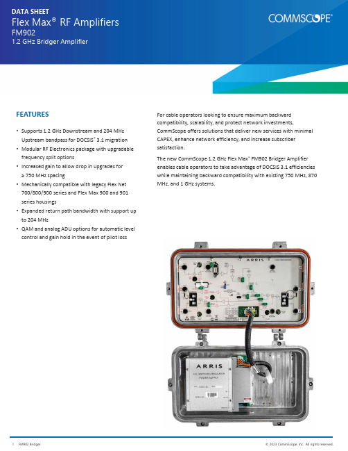
DATA SHEET Flex Max ®RF Amplifiers FM9021.2 GHz Bridger AmplifierFor cable operators looking to ensure maximum backward compatibility, scalability, and protect network investments, CommScope offers solutions that deliver new services with minimal CAPEX, enhance network efficiency, and increase subscriber satisfaction.The new CommScope 1.2 GHz Flex Max ®FM902 Bridger Amplifier enables cable operators to take advantage of DOCSIS 3.1 efficiencies while maintaining backward compatibility with existing 750 MHz, 870 MHz, and 1 GHz systems.•Supports 1.2 GHz Downstream and 204 MHzUpstream bandpass for DOCSIS ®3.1 migration•Modular RF Electronics package with upgradablefrequency split options•Increased gain to allow drop in upgrades for≥ 750 MHz spacing•Mechanically compatible with legacy Flex Net700/800/900 series and Flex Max 900 and 901series housings•Expanded return path bandwidth with support upto 204 MHz•QAM and analog ADU options for automatic levelcontrol and gain hold in the event of pilot loss FEATURESDownstreamThe new FM902 Bridger amplifier is equipped with Gallium Nitride (GaN) technology and two high level driven RF outputs. Each output port can be split with optional plug‐in Distribution accessories to enable a total of four ports.New 1.2 GHz Forward Cable Equalizers (CE‐120‐*) and Cable Simulators (CS‐120‐*) are available to optimize system designs. These new plug‐ins are in the JXP‐style form factor and plug into a carrier board with a backward compatible footprint so that operators who want to use the new amplifiers in older 870 MHz or 1 GHz systems can re‐use their SEQ‐* equalizers. The FM902 utilizes pluggable diplex filters, which provides operators with the flexibility to change band splits in the future.The following frequency splits are available:•5 to 42 MHz/54 to 1218 MHz (042 split)•5 to 85 MHz/102 to 1218 MHz (085 split)•5 to 204 MHz/258 to 1218 MHz (204 split)The FM902 is available pre‐configured with multiple Automatic Level Control (ALC) options that include 499.25 MHz for analog pilots or 609 MHz and 711 MHz for QAM pilot frequencies. These new pluggable Drive units are not backward compatible with previous FlexMax amplifiers. All amplifiers feature an Automatic/Manual mode jumper that can be set to enable the amplifier to operate in a Manual Level Control (MLC) or Thermal Gain Control (TGC) mode. The amplifier utilizes a gain hold feature in the event of pilot loss for added system reliability. There is an LED indicator to provide visual confirmation of the selected mode and pilot presence.UpstreamThe FM902 features 27 dB of gain in the upstream to accommodate a variety of network designs including high split. The upstream circuitry includes an attenuator location prior to the input test points that allows operators to achieve the recommended input levels. The return equalizer maintains the legacy MEQ‐**‐* form factor from the Flex Max series amplifiers and operators can select from a range of values based on their network design. Previous generation MEQT return path equalizers are no longer required because of the FM902’s on‐board thermal compensation feature, which helps maintain levels over temperature. There is also a new plug‐in Low Pass filter to provide additional high frequency signal isolation from the downstream signal path.Backward CompatibilityThe FM902 is available as a complete amplifier station or as a drop‐in RF module for economical upgrades of legacy C‐COR 750 MHz and 870 MHz FlexNet bridger amplifiers or FM901 1 GHz amplifiers. The FM902 features internal ‐20 dB test points only; there is no option for external test points. The RF module, however, can be installed into an earlier housing that does support external test points without invoking mechanical interference.COMPATIBILITY700900900901 Upgrade to Flex Max FM902Yes Yes Yes Yes Yes204 Split258–1218 Flatness, dB2±1.0 Operational Gain, dB347 minInternal Slope, dB4042 Split085 Split204 Split 21.0 19.4 15.5Noise Figure, dB8Test Points, dB‐20 ±1.0 Return Loss, dB516Hum Modulation @ 15A, dBc6 F minfwd to 870 MHz871 to 1003 MHz1004 to 1218 MHz ‐60‐55‐50Distortion: 1.2 GHz Analog/Digital, 30 Analog/124 Digital Channels7Reference Frequency, MHz1218/258/54Reference Input Level, dBmV10/8.2/10 (virtual)Reference Output Level (21 dB Slope), dBmV57/39.7/36 (virtual)Composite Triple Beat (CTB), dBc‐70Composite Second Order (CSO), dBc‐76Carrier to Composite Noise (CCN), dB856Distortion: 1.2 GHz All Digital, 190 Digital ChannelsReference Frequency, MHz1218/258/54Reference Input Level, dBmV4/2.2/4 (actual)Reference Output Level (21 dB Slope), dBmV51/33.7/30 (actual)Carrier to Composite Noise (CCN), dB849Modulation Error Rate (MER), dB948 minNOTES:1.Downstream bandwidth is determined by the diplex filters, forward flatness correction board, and high pass filter installed in the amplifier.2.Flatness is measured with respect to slope. Slope is calculated using least squares.3.Includes forward equalizer loss and gain reserve for proper AGC operation.4.Specified from 54 to 1218 MHz,5.0 dB Linear Slope plus 16.0 dB Cable Slope.5.Measured with jumpers in the Distribution accessory location.6.Hum modulation is measured at 15 Amps AC current passing through the port under test (13 Amps AC for ports 2 and 5).7.30 analog channels from 55.25 MHz to 253.25 MHz, 124 digital QAM channels from 261 MHz to 999 MHz, and a 192 MHz wide OFDM channel centered at 1122 MHz. The digitalchannels are at a level 6 dB below the analog. The output level is 57 dBmV (virtual) at 1218 MHz, with 21 dB tilt from 54 MHz to1218 MHz.N is measured by turning off the QAM/OFDM channel under test and inserting a CW test signal at the corresponding QAM/OFDM RF level in its place.9.The MER is calculated from the measured CCN.SPECIFICATIONSAC Input Current (Typical) 1.0 A/36 W @ 45 V0.8 A/36 W @ 60 V0.7 A/37 W @ 90 VAC Input Voltage Range, VAC 40–90AC Bypass Current, A1513 (Port 2 and Port 5)Operating Temperature Range‐40°to +60°C ‐40°to +140°F Housing Dimensions, L x W x D16.0 L x 10.7 W x 5.35 D inches 406 L x 272 W x 136 D mm Weight 16 lbs7.3 kg204 Split 5–204Flatness, dB 2±0.5Operational Gain, dB 327Reference Operating Slope, dB 0 ±0.75Noise Figure, dB 48Test Points, dB ‐20 ±1.0Return Loss, dB 5,616Hum Modulation @ 15A, dBc 75 to 10 MHz11 to F maxreturn MHz ‐50‐60Distortion: All Digital, 6 Digital Channels 8Reference Frequency, MHz42/5Reference Input Level, dBmV13/13Reference Output Level, dBmV40/40NPR Dynamic Range, dB 929BER Dynamic Range, dB 1035Distortion: All Digital, 13Digital Channels 8Reference Frequency, MHz85/5Reference Input Level, dBmV9/9Reference Output Level, dBmV36/36NPR Dynamic Range, dB 926BER Dynamic Range, dB 1032Distortion: All Digital, 33 Digital Channels 8Reference Frequency, MHz204/5Reference Input Level, dBmV6/6Reference Output Level, dBmV33/33NPR Dynamic Range, dB 922BER Dynamic Range, dB 1028NOTES:1.Upstream bandwidth is determined by the diplex filters, low pass filter (RPLPF), and upstream equalizer (MEQ) installed in the amplifier.2.Flatness is measured with respect to slope. Slope is calculated using Least Squares.3.Includes return equalizer loss and gain reserve for proper AGC operation.4.Noise figure is at T a = 25 ±5°C. The noise figure may degrade by up to 1 dB over the operating temperature range and will degrade by 3 dB typical when a Splitter is installed in the Distribution accessory location.5.The return loss from 5–15 MHz may degrade by up to 1 dB over the operating temperature range.6.Measured with jumpers in the Distribution accessory location.7.Hum modulation is measured with 15 Amps AC current passing through the port under test (13 Amps AC current for ports 2 and 5). Hum mode can degrade by up to 5 dB from 5–10 MHz at ‐40°C.8.The QAM load is 256 QAM, J.83 Annex B, 5.360537 MS/s; 6 MHz/channel.9.The NPR dynamic range is specified for an NPR greater than or equal to 40 dB.10.The BER dynamic range is specified for an uncorrected (Pre ‐FEC) BER less than or equal to 1.0 x 10‐6.Note: Specifications are subject to change without notice.Copyright Statement:©2022CommScope,Inc.All rights reserved.ARRIS,the ARRIS logo,and Flex Max are trademarks of CommScope,Inc.and/or its affiliates.All other trademarks are the property of their respective owners.No part of this content may be reproduced in any form or by any means or used to make any derivative work (such as translation,transformation,or adaptation)without written permission from CommScope,Inc and/or its affiliates (“CommScope”).CommScope reserves the right to revise or change this content from time to time without obligation on the part of CommScope to provide notification of such revision or change.Contact Technical Services for product support:•United States: +1‐888‐944‐4357•International: +1‐215‐323‐2345RELATED PRODUCTSADU/QADUSS ‐1218‐2 Splitters FM332 1.2 GHz Line ExtenderInstallation Services SDC ‐1218‐* DirectionalCouplers Forward Signal Correction Plug ‐in Accessories1.2 GHz FM902 BRIDGER AMPLIFIER ORDERING GUIDEIn the example below, part number FMB12X085‐SHG6C1N corresponds to the shaded rows in the Key Guide.F M B 12X 085—S HG 6C 1N REQUIRED ACCESSORIESModel NameDescription CE ‐120‐*CS ‐120‐*Forward 1.2GHzCableEqualizer 2 to 20 dB in 1 dB steps ‐or ‐Forward 1.2 GHz Cable Simulator 1 to 10 dB in 1 dB steps MEQ ‐**‐*Return Equalizer, 5–42 MHz (042 Split), 5–85 MHz (085 Split), 5–204 MHz (204 Split)NPB ‐*NPB ‐750Plug ‐in attenuator/pad (values 0 to 26 dB in 1 dB steps)Plug ‐in terminator (75 ohm)。
MP902技术规格书

MP902产品技术规范版本V ersion:V1.00发布日期Date:18/4/2008文件编号Document Number:xxxx深圳梦网科技发展有限公司本文档适用的产品是MP902彩信监控器。
本文档以MP902产品为例,主要介绍MP902产品的外观、硬件结构、功能、技术规格和模块有关指标的测试标准,用于帮助市场技术支持工程师提供技术支持及测试人员测试提供参考。
阅读对象本文档主要适用于以下工程师:产品工程师市场技术支持工程师测试工程师修改记录修订记录累积了每次文档更新的说明。
最新版本的文档包含以前所有文档版本的更新内容。
文档版本V1.0 (2008-04-18)第一次正式发布。
目录1 产品简介 (1)2 缩略语 (1)3外观和结构 (2)4功能 (3)4.1主要功能定义 (3)5主要技术规格 (4)5.1通讯协议及技术指标 (4)5.2射频接收 (4)5.3遥控接收 (4)5.4天线 (4)5.5主要性能指标 (5)5.6待机时间 (5)5.7工作条件 (5)6可靠性测试标准 (6)6.1跌落实验 (6)6.2振动实验 (6)6.3低温运行实验 (6)6.4低温存储实验 (7)6.5高温运行实验 (7)6.6高温存储实验 (7)6.7高温高湿实验 (8)6.8高低温冲击实验 (8)7 EMC/EMI测试标准 (8)7.1静电放电试验(ESD) (8)7.2射频电磁场辐射抗扰性试验 (9)7.3电快速瞬变脉冲群抗扰性试验 (9)7.4雷击浪涌抗扰性试验 (10)7.5射频电磁场传导抗扰性试验 (10)7.6电压瞬时跌落和短时中断的抗扰性试验 (11)7.7辐射发射试验 (11)8引用标准 (11)9产品齐套 (12)1产品简介深圳梦网科技发展有限公司是一家生产GSM/CDMA无线终端产品的国内知名企业,是国内最早开发和批量生产GSM、CDMA无线终端产品的厂商,拥有多年的研发与生产经验。
V90-B1.1彩信监控器是利用图像移动侦测和被动红外人体感应技术,将监控现场的异常用摄像头拍摄下来,经图像压缩,再经GSM模块通过移动通信网的彩信服务、GPRS功能,将现场拍摄到的画面传输到指定用户手机、邮箱或互联网管理平台的无线监控设备。
MEMORY存储芯片S9012中文规格书
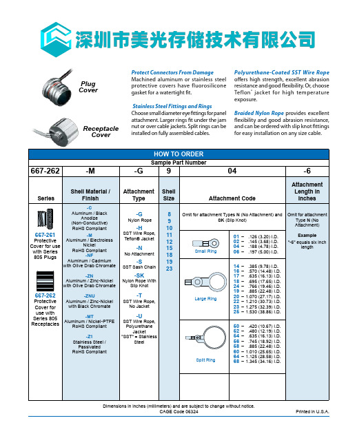
01-JANUARY-2010Dimensions in inches (millimeters) and are subject to change without notice.CAGE Code 06324Printed in U.S.A.Protect Connectors From DamageMachined aluminum or stainless steel protective covers have fluorosilicone gasket for a watertight fit.Stainless Steel Fittings and RingsChoose small diameter eye fittings for panel attachment. Larger rings fit under the jam nut or over cable jackets. Split rings can be installed on fully assembled cables.Polyurethane-Coated SST Wire Rope offers high strength, excellent abrasion resistance and good flexibility. Or, choose Teflon ® jacket for high temperature exposure.Braided Nylon Rope provides excellent flexibility and good abrasion resistance, and can be ordered with slip knot fittings for easy installation on any size cable.Plug CoverReceptacle CoverDimensions in inches (millimeters) and are subject to change without notice.CAGE Code 06324Printed in U.S.A.-SEPTEMBER -2011Dimensions in inches (millimeters) and are subject to change without notice.CAGE Code 06324Printed in U.S.A.polyurethane Coated Wire Rope Black polyurethane over stainless steel rope, -55° to +125°C., very flexible, excellent abrasion resistance, excellent resistance tofuels, .080" (2mm) diameterteflon ® Jacketed Wire RopeTranslucent FEP jacket over stainless steel, -55° to +200°C., fair flexibility, good abrasion resistance, .100" diameterSash ChainSlip Knot (SK)Dimensions in inches (millimeters) and are subject to change without notice.CAGE Code 06324 Printed in U.S.A.。
- 1、下载文档前请自行甄别文档内容的完整性,平台不提供额外的编辑、内容补充、找答案等附加服务。
- 2、"仅部分预览"的文档,不可在线预览部分如存在完整性等问题,可反馈申请退款(可完整预览的文档不适用该条件!)。
- 3、如文档侵犯您的权益,请联系客服反馈,我们会尽快为您处理(人工客服工作时间:9:00-18:30)。
CN16 (14PIN/2.0) 按键板接口定义(预留)
脚序号 1 2 3 4
定义 VDD IR GND K7
13
描述 5V 电源 遥控接收 地 Power 键
5 6 7 LED-G GND K6 K5 K4 K3 K2 K1 K0
16 17 18 19 20
SCL HDMI-5V GND GND HPD
0 0 Ground Ground 0
CLOCK 5V 地 地 HPD
CN10(34PIN/2.0)液晶屏接口(LVDS 信号格式)
脚序号 1 2 3 4 5 6 7 8 9 10 11 12 13 14 15
定义 VCC VCC VCC GND GND GND RXO0RXO0+ RXO1RXO1+ RXO2RXO2+ GND GND RXOC-
类型 Power Power Power Ground Ground Ground 0 0 0 0 0 0 Ground Ground 0
11
描述 Power for Panel Power for Panel Power for Panel ------LVDS ODD 0 - Signal LVDS ODD 0 + Signal LVDS ODD 1 - Signal LVDS ODD 1 + Signal LVDS ODD 2 - Signal LVDS ODD 2 + Signal ----LVDS ODD Clock - Signal
深圳市双宝莱电子科技有限公司
Shen Zhen Shuang Bao Lai Technology co.,Ltd.
DID 液晶拼接墙 驱动板规格书
(板卡型号:SBL-902C V1.2)
文件编号:
201500801002
版本信息: 编 审 复 批
V1.2
制: 詹春龙 核: 赵明明 审: 准:
李秀潮
CN8(10PIN/2.5 4) 电源接口
7 8 9 10
GND GND +12V +12V
地 地 12V 电源输入 12V 电源输入
CNH1(20PIN) HDMI 信号接口
脚序号 1 4 3 4 5 6 7 8 9 10 11 12 13 14 15
定义 D2+ GND D2D1+ GND D1D0+ GND D0CLK+ GND CLKNC CEC SDA
CN6/CN7
CN8
*CN11
CN15
CN21 CN14 CN20 *CNH1
8
注: 上图带*为预留接口
*CN17
*CN12
*CN16
CN19
CN2(2PIN/2.0) 温度传感器信号输入
1 2 GND ADC GND 传感
CN3(6PIN/2.0) INVERTER 接口
脚序号 1 2 3 4 5 6 定义 12V 12V ONOFF ADJ GND GND 描述 直流电源 直流电源 INVERTER 开关控制(高电平有效) 亮度调节 地 地
红色指示灯 绿色指示灯 地 Up Down 输入切换键 Menu 键 LEFT RIGHT 备用
接
口
输入
DVI VGA AV USB
输出
PANEL 接口 AV OUT
LVDS34Pin/2.0 直式金针插座 视频输出 DC 12V+5V 5V/12V 正常工作模式 待机功耗<1W 无
输入电源 电 源 驱屏电压 电源操作 电源管理 功放 其 他 按键控制 OSD 语言
MENU,POWER, SOURCE,LEFT,RIGHT,UP,DOWN
640×350/70 720×400/70 640×480/60 640×480/72 800×600/60 800×600/70 800×600/72 800×600/75
31.469 31.469 31.469 37.861 37.879 44.490 48.077 46.875
9 10 11 12 13 14 15 16 17 18 19 20
-/-/-/+/ +/ +/ +/ +/ +/
4、产品 PCB 尺寸及结构图说明
见后面附图 PCB 尺寸说明: * PCB 厚度加最高零件高:16mm * PCB 长度:222.50mm * PCB 宽度:108.00mm * PCB 螺丝孔径:直径 3.5mm
7
5、主要接口定义说明
USB
HDMI
CN6、CN7(3PIN/2.5 4) 风扇电源控制
1 2 3 脚序号 1 2 3 4 5 6
+12V +12V GND 定义 STB GND GND +5V/S +5V +5V
9
FAN VCC FAN VCC GND 描述 STANDBY 地 地 5V(0.5A) 5V 电源输入 5V 电源输入
60.004 70.069 72.000 75.029 59.870 74.893 57.030 75.025 59.799 59.901 59.883 59.883
65.000 75.000 77.000 78.750 79.500 102.250 100.000 135.000 84.750 88.750 119.000 189.750
中文、英文
3、 显示模式
◆ 以下的显示模式表,涵盖了本产品所能支持的所有的显示模式;如果 不 在该表之内的显示模式,产品不能确保正常工作。
5
◆ 该表已经覆盖我们大部分常用的显示模式,尤其是 VESA 标准定义的 显 示模式都在支持之列。如果用户有要求显示一些特殊的显示模式,也可 以根据 用户提供的数据将其设置在支持之列。 ◆ 并非每一个具体的应用都能处理显示模式表中的所有模式,需要根 据 PANEL 的尺寸、分辨率以及一些关键参数进行选择。 ◆ 大部分的 PANEL 都不支持垂直刷新率在 75Hz 以上的应用,这些模式 A/D 板大多都能处理, 但是应用高过 PANEL 限制的显示模式可能会导致 PANEL 损坏。 ◆ 针对 LCD 显示器的特殊性,只有输入显示模式的分别率和 PANE 显示 分辨率相对应时,才会有最佳的显示性能。例如大部分 55 寸 PANEL 的分辨 率 是 1920×1080, 那么只有输入的显示模式分辨率是 1920×1080 才会有最 佳的显示 效果。 序号 显示模式 水平同步频率 kHz 1 2 3 4 5 6 7 8
DVI
VGA
AV IN
AV OUT
RS232/IR IN(Debug)
RS232/IR OUT
可选双 AV 配置(预留) AV2 IN USB HDMI DVI VGA AV1 IN AV2 OUT AV1 OUT RS232/IR IN(Debug) RS232/IR OUT
CN10
CN2 CN3
类型 0 Ground 0 0 Ground 0 0 Ground 0 时钟 Ground 时钟 0 0 0
10
描述 D2+Signal 地 D2-Signal D1+Signal 地 D1-Signal D0+Signal 地 D0-Signal Clock+Signal 地 Clock-Signal 空 CEC DATA
0 0 0 0 0 0 0 0 0 Ground Ground 0 0 0 0 0 0 0 0
LVDS ODD Clock + Signal LVDS ODD 3 - Signal LVDS ODD 3 + Signal LVDS EVEN 0 - Signal LVDS EVEN 0+ Signal LVDS EVEN 1 - Signal LVDS EVEN 1 + Signal LVDS EVEN 2 - Signal LVDS EVEN 2 + Signal ----LVDS EVEN Clock - Signal LVDS EVEN Clock + Signal LVDS EVEN 3 - Signal LVDS EVEN 3 + Signal LVDS EVEN 4 - Signal LVDS EVEN 4 + Signal LVDS ODD 4 - Signal LVDS ODD 4 + Signal
16 17 18 19 20 21 22 23 24 25 26 27 28 29 30 31 32 33 34
RXOC+ RXO3RXO3+ RXE0RXE0+ RXE1RXE1+ RXE2RXE2+ GND GND RXECRXEC+ RXE3RXE3+ RXE4RXE4+ RXO4RXO4+
垂直同步频率 Hz 70.087 70.087 59.941 72.809 60.317 70.000 72.188 75.000
6
像素时钟 MHz 25.175 28.322 25.175 31.500 40.000 44.850 50.000 49.500
同步信号 极性 +/ -/-/+/ +/ +/ +/
12
CN11(10PIN/2.0)
脚序号 1 2 3 4 5 6 7 8 9 10 12V 12V
IIC 接口(预留)
描述 12V 电源 12V 电源 地 地 5V 电源 5V 电源 地 时钟 数据 IO 口
定义
GND GND 5V 5V GND SCL SDA GPIO
CN12(3PIN/2.0)声音输出口(预留)