MAX682中文资料
MAX471MAX472的中文资料大全

M A X471M A X472的中文资料大全(总4页)-本页仅作为预览文档封面,使用时请删除本页-MAX471/MAX472的特点、功能美国美信公司生产的精密高端电流检测放大器是一个系列化产品,有MAX471/MA X472、 MAX4172/MAX4173等。
它们均有一个电流输出端,可以用一个电阻来简单地实现以地为参考点的电流/电压的转换,并可工作在较宽电压内。
MAX471/MAX472具有如下特点:●具有完美的高端电流检测功能;●内含精密的内部检测电阻(MAX471);●在工作温度范围内,其精度为2%;●具有双向检测指示,可监控充电和放电状态;●内部检测电阻和检测能力为3A,并联使用时还可扩大检测电流范围;●使用外部检测电阻可任意扩展检测电流范围(MAX472);●最大电源电流为100μA;●关闭方式时的电流仅为5μA;●电压范围为3~36V;●采用8脚DIP/SO/STO三种封装形式。
MAX471/MAX472的引脚排列如图1所示,图2所示为其内部功能框图。
表1为MAX471/MAX472的引脚功能说明。
MAX471的电流增益比已预设为500μA/A,由于2kΩ的输出电阻(ROUT)可产生1V/A的转换,因此±3A时的满度值为3V.用不同的ROUT电阻可设置不同的满度电压。
但对于MAX471,其输出电压不应大于VRS+。
对于MAX472,则不能大于。
MAX471引脚图如图1所示,MAX472引脚图如图2所示。
MAX471/MAX472的引脚功能说明引脚名称功能MAX471MAX47211SHDN关闭端。
正常运用时连接到地。
当此端接高电平时,电源电流小于5μA2,3-RS+内部电流检测电阻电池(或电源端)。
“+”仅指示与SIGN输出有关的流动方向。
封装时已将2和3连在了一起-2空脚-3RG1增益电阻端。
通过增益设置电阻连接到电流检测电阻的电池端44GND地或电池负端55SIGN集电极开路逻辑输出端。
MAX232中文资料,MAX232CPE,MAX232EPE,MAX232ECPE,规格书,MAXIM代理商,datasheet,PDF
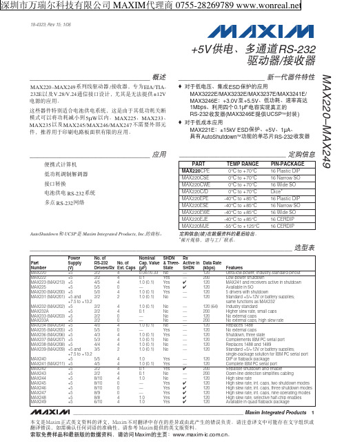
19-4323; Rev 15; 13;5V ޥ٫Ăۂ لRS-232 ഝڑಹ/ेฏಹ
________________________________ ݣะ
MAX220–MAX249࿅઼ഝڑಹ /ेฏಹLjከཛྷEIA/TIA232EჾࣆV.28/V.24ဳेਊහࣜLjᅐದกྐۨ໗ ޥ±12V ٫ᆚوᄮᅋă
ሦဗಹऔ໎Ӽคࠩ٫֠ޥ٫࿅༇Ljሦกᅑᅢದّڱߔࠞޢ ன৹ჾटࠞޢऋဏ ف5μW ჾăMAX225ĂMAX233Ă MAX235 ჾࣆ MAX245/MAX246/MAX247 ԥၖე༶ԩᆐ औLj༚ऌᅋᅢᄩฺ٫ଁғஎࢵᅘوᄮᅋă
1.0 (0.1) 0.1 — — 1.0 (0.1) — 1.0 (0.1) 1.0 (0.1) 1.0 (0.1) 1.0 (0.1)
1.0 1.0 (0.1) 0.1 0.1 1.0 — — — 1.0 1.0
SHDN & ThreeState No Yes Yes Yes Yes No
No No No No No Yes Yes No No No
_____________________________________________________________________ ၭျӹ
Part Number MAX220 MAX222 MAX223 (MAX213) MAX225 MAX230 (MAX200) MAX231 (MAX201)
MAX232 (MAX202) MAX232A MAX233 (MAX203) MAX233A MAX234 (MAX204) MAX235 (MAX205) MAX236 (MAX206) MAX237 (MAX207) MAX238 (MAX208) MAX239 (MAX209)
MAX882中文资料
19-0275; Rev 0; 12/94
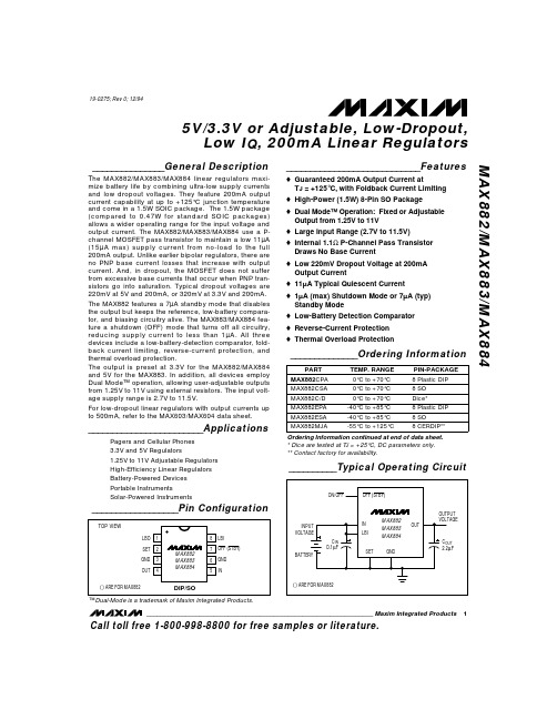
5V/3.3V or Adjustable, Low-Dropout, Low IQ, 200mA Linear Regulators
_______________General Description
The MAX882/MAX883/MAX884 linear regulators maximize battery life by combining ultra-low supply currents and low dropout voltages. They feature 200mA output current capability at up to +125°C junction temperature and come in a 1.5W SOIC package. The 1.5W package (compared to 0.47W for standard SOIC packages) allows a wider operating range for the input voltage and output current. The MAX882/MAX883/MAX884 use a Pchannel MOSFET pass transistor to maintain a low 11µA (15µA max) supply current from no-load to the full 200mA output. Unlike earlier bipolar regulators, there are no PNP base current losses that increase with output current. And, in dropout, the MOSFET does not suffer from excessive base currents that occur when PNP transistors go into saturation. Typical dropout voltages are 220mV at 5V and 200mA, or 320mV at 3.3V and 200mA. The MAX882 features a 7µA standby mode that disables the output but keeps the reference, low-battery comparator, and biasing circuitry alive. The MAX883/MAX884 feature a shutdown (OFF) mode that turns off all circuitry, reducing supply current to less than 1µA. All three devices include a low-battery-detection comparator, foldback current limiting, reverse-current protection, and thermal overload protection. The output is preset at 3.3V for the MAX882/MAX884 and 5V for the MAX883. In addition, all devices employ Dual Mode™ operation, allowing user-adjustable outputs from 1.25V to 11V using external resistors. The input voltage supply range is 2.7V to 11.5V. For low-dropout linear regulators with output currents up to 500mA, refer to the MAX603/MAX604 data sheet.
MAX320-MAX322中文资料
ELECTRICAL CHARACTERISTICS
(V+ = +5V ±10%, V- = -5V ±10%, VINH = 3.5V, VINL = 2.5V, TA = TMIN to TMAX, unless otherwise noted.)
PARAMETER ANALOG SWITCH Analog Signal Range
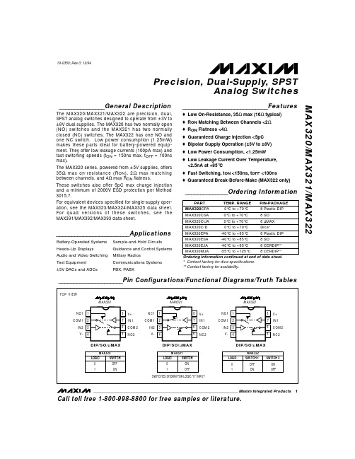
For equivalent devices specified for single-supply operation, see the MAX323/MAX324/MAX325 data sheet. For quad versions of these switches, see the MAX391/MAX392/MAX393 data sheet.
Plastic DIP (derate 9.09mW/°C above +70°C) .............727mW Narrow SO (derate 5.88mW/°C above +70°C) .............471mW
µMAX (derate 4.10mW/°C above +70°C) .....................330mW CERDIP (derate 8.00mW/°C above +70°C) ..................640mW Operating Temperature Ranges MAX32_C_ _ ........................................................0°C to +70°C MAX32_E_ _......................................................-40°C to +85°C MAX32_MJA ...................................................-55°C to +125°C Storage Temperature Range .............................-65°C to +150°C Lead Temperature (soldering, 10sec) .............................+300°C
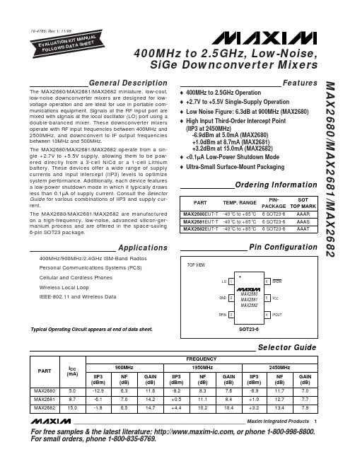
MAX2680-MAX2682中文资料
ICC
ICC VIH VIL ISHDN
MAX2680 MAX2681 MAX2682 SHDN = 0.5V
0 < SHDN < VCC
5.0
7.7
8.7
12.7
mA
15.0 21.8
0.05
5
µA
2.0
V
0.5
V
0.2
µA
AC ELECTRICAL CHARACTERISTICS
(MAX2680/1/2 EV Kit, VCC = SHDN = +3.0V, TA = +25°C, unless otherwise noted. RFIN and IFOUT matched to 50Ω. PLO = -5dBm, PRFIN = -25dBm.)
DC ELECTRICAL CHARACTERISTICS
(VCC = +2.7V to +5.5V, SHDN = +2V, TA = TMIN to TMAX unless otherwise noted. Typical values are at VCC = +3V and TA = +25°C. Minimum and maximum values are guaranteed over temperature by design and characterization.)
10
500 MHz
Conversion Power Gain
fRF = 400MHz, fLO = 445MHz, fIF = 45MHz fRF = 900MHz, fLO = 970MHz, fIF = 70MHz fRF = 1950MHz, fLO = 1880MHz, fIF = 70MHz (Note 1) fRF = 2450MHz, fLO = 2210MHz, fIF = 240MHz
max2器件中文手册

MAX1968-MAX1969中文资料
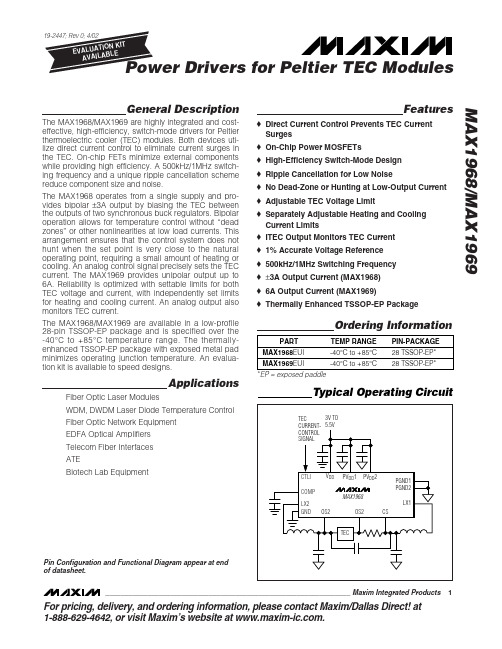
19-2447; Rev 0; 4/02
KIT ATION EVALU E L B A AVAIL
Power Drivers for Peltier TEC Modules
General Description Features
o Direct Current Control Prevents TEC Current Surges o On-Chip Power MOSFETs o High-Efficiency Switch-Mode Design o Ripple Cancellation for Low Noise o No Dead-Zone or Hunting at Low-Output Current o Adjustable TEC Voltage Limit o Separately Adjustable Heating and Cooling Current Limits o ITEC Output Monitors TEC Current o 1% Accurate Voltage Reference o 500kHz/1MHz Switching Frequency o ±3A Output Current (MAX1968) o 6A Output Current (MAX1969) o Thermally Enhanced TSSOP-EP Package
Fiber Optic Laser Modules WDM, DWDM Laser Diode Temperature Control Fiber Optic Network Equipment EDFA Optical Amplifiers Telecom Fiber Interfaces ATE Biotech Lab Equipment
amc6821中文资料

AMC6821智能温度控制器、PWM控制器特征远程温度传感器:精度±2°C、分辨率0.125°C局部温度传感器:精度±2°C、分辨率0.125°CPWM控制器PWM频率:10Hz到40kHz、占空比:0%到10%、8位自动风扇速度控制回路SMBus接口供电:2.7V到5.5V封装(绿色):QSOP-16(4mmx5mm)符合RoHS应用笔记本和台式机网络服务器电讯设备PC-Based设备DLPTM和LCD投影仪描述AMC6821是一款智能温度控制和PWM控制器。
其设计用于需要启动系统降温噪声敏感和功率敏感应用。
使用一个低频或高频PWM信号,这个器件可以同时驱动一个风扇监控远程传感器温度,测量和控制风扇速度以便运行在最小噪音和最小速度下。
AMC6821 有三种风扇控制模式:自动温度风扇控制模式,软控RPM模式,软控DCY模式。
每种模式通过改变PWM输出占空比控制电机速度。
自动温度风扇控制模式是一种智能、闭环控制,根据用户定义参数优化风扇速度。
这种模式允许AMC6821作为独立运行器件,不需要中断CPU;风扇可以连续控制(基于温度测量)即使CPU或系统锁定。
软控RPM模式是一个二阶闭环控制。
在这种模式下,AMC6821调整PWM输出以维持用户精确设定的一致的电机速度;换而言之,这个器件作为风扇速度校准。
第三种模式,软控DCY模式,是开环回路。
在软控DCY模式下,PWM占空周期直接通过写入器件数值来设定。
AMS6821有一个可编程SMBALERT输出来指示错误条件和专用FAN-FAULT输出来指示电机错误。
THERM管脚是一个过温条件容错输出,可以用于压制CPU时钟。
此外,OVR管脚同样指示过温限制。
所有报警门限通过器件寄存器设定。
内部框图绝对最大额定值器件封装节点功能SMBUS接口AMC6821通过SMBus通信。
AMC6821作为从机接入总线,通过一个总线监控控制。
MAX31865中文资料_数据手册_参数

VIL
CS, SDI, SCLK
Input Logic 1
Analog Voltages (FORCE+,FORCE2, FORCE-, RTDIN+, RTDIN-) Reference Resistor Cable Resistance
VIH
CS, SDI, SCLK
Normal conversion results
MAX31865 RTD-to-Digital Converter
ABSOLUTE MAXIMUM RATINGS
Voltage Range on VDD Relative to GND1.............-0.3V to +4.0V Voltage Range on BIAS, REFIN+,
Applications
Industrial Equipment Medical Equipment Instrumentation
Ordering Information appears at end of data sheet.
For related parts and recommended products to use with this part, refer to /MAX31865.related.
PACKAGE THERMAL CHARACTERISTICS (Note 1)
TQFN Junction-to-Ambient Thermal Resistance (qJA)...........29°C/W Junction-to-Case Thermal Resistance (qJC)..................2°C/W
EVALUATION KIT AVAILABLE
MAX232中文资料(官方版)
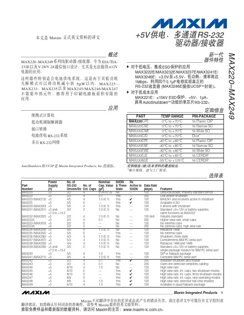
新一代 器件特性 ____________________________
♦ 对于低电压、集成 ESD 保护的应用 MAX3222E/MAX3232E/MAX3237E/MAX3241E/ MAX3246E:+3.0V 至 +5.5V、低功耗、速率高达 1Mbps、利用四个 0.1µF 电容实现真正的 RS-232 收发器 (MAX3246E 提供 UCSPTM 封装 )。 ♦ 对于低成本应用 MAX221E:±15kV ESD 保护、+5V、1µA、 具有 AutoShutdownTM 功能的单芯片 RS-232。
________________________________ 应用
便携式计算机 低功耗调制解调器 接口转换 电池供电 RS-232 系统 多点 RS-232 网络
_____________________________ 定购信息
PART MAX220CPE MAX220CSE MAX220CWE MAX220C/D MAX220EPE MAX220ESE MAX220EWE MAX220EJE MAX220MJE TEMP RANGE 0°C to +70°C 0°C to +70°C 0°C to +70°C 0°C to +70°C -40°C to +85°C -40°C to +85°C -40°C to +85°C -40°C to +85°C -55°C to +125°C PIN-PACKAGE 16 Plastic DIP 16 Narrow SO 16 Wide SO Dice* 16 Plastic DIP 16 Narrow SO 16 Wide SO 16 CERDIP 16 CERDIP
MAX706中文简介

功能监控器MAX705/706/813中文资料。
概述MAX705/706/813L是一组CMOS监控电路,能够监控电源电压、电池故障和微处理器(MPU或mP)或微控制器(MCU或mC)的工作状态。
将常用的多项功能集成到一片8脚封装的小芯片内,与采用分立元件或单一功能芯片组合的电路相比,大大减小了系统电路的复杂性和元器件的数量,显著提高了系统可靠性和精确度。
该系列产品采用3种不同的8脚封装形式:DIP、SO和mMAX。
主要应用于:微处理器和微控制器系统;嵌入式控制器系统;电池供电系统;智能仪器仪表;通信系统;寻呼机;蜂窝移动电话机;手持设备;个人数字助理(PDA);电脑电话机和无绳电话机等等。
功能说明RESET/RESET操作复位信号用于启动或者重新启动MPU/MCU,令其进入或者返回到预知的循环程序并顺序执行。
一旦MPU/MCU处于未知状态,比如程序“跑飞”或进入死循环,就需要将系统复位。
对于MAX705和MAX706而言,在上电期间只要Vcc大于,就能保证输出电压不高于的低电平。
在Vcc上升期间RESET维持低电平直到电源电压升至复位门限或以上。
在超过此门限后,内部定时器大约再维持200ms后释放RESET,使其返回高电平。
无论何时只要电源电压降低到复位门限以下(即电源跌落),RESET引脚就会变低。
如果在已经开始的复位脉冲期间出现电源跌落,复位脉冲至少再维持140ms。
在掉电期间,一旦电源电压Vcc降到复位门限以下,只要Vcc不比还低,就能使RESET维持电压不高于的低电平。
MAX705和MAX706提供的复位信号为低电平RESET,而MAX813L提供的复位信号为高电平RESET,三者其它功能完全相同。
有些单片机,如INTEL的80C51系列,需要高电平有效的复位信号。
看门狗定时器MAX705/706/813L片内看门狗定时器用于监控MPU/MCU的活动。
如果在内WDI端没有收到来自MPU/MCU 的触发信号,并且WDI处于非高阻态,则WDO输出变低。
MAX2560中文资料
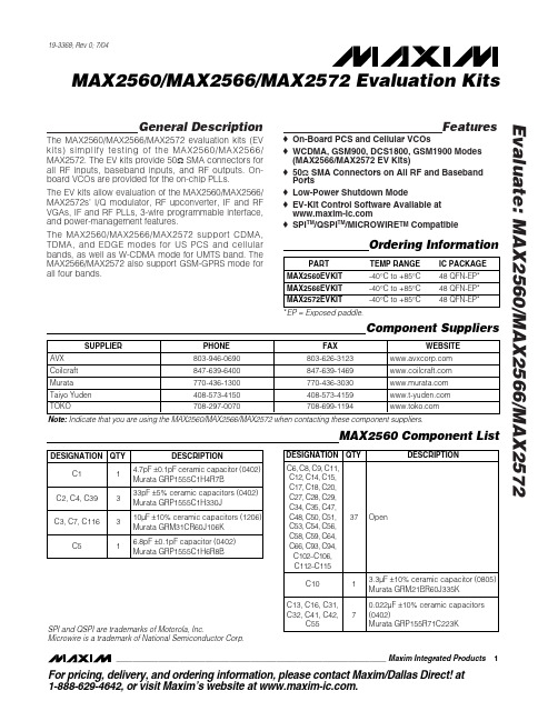
General DescriptionThe MAX2560/MAX2566/MAX2572 evaluation kits (EV kits) simplify testing of the MAX2560/MAX2566/MAX2572. The EV kits provide 50ΩSMA connectors for all RF inputs, baseband inputs, and RF outputs. On-board VCOs are provided for the on-chip PLLs.The EV kits allow evaluation of the MAX2560/MAX2566/MAX2572s’ I/Q modulator, RF upconverter, IF and RF VGAs, IF and RF PLLs, 3-wire programmable interface,and power-management features.The MAX2560/MAX2566/MAX2572 support CDMA,TDMA, and EDGE modes for US PCS and cellular bands, as well as W-CDMA mode for UMTS band. The MAX2566/MAX2572 also support GSM-GPRS mode for all four bands.Features♦On-Board PCS and Cellular VCOs♦WCDMA, GSM900, DCS1800, GSM1900 Modes (MAX2566/MAX2572 EV Kits)♦50ΩSMA Connectors on All RF and Baseband Ports♦Low-Power Shutdown Mode♦EV-Kit Control Software Available at ♦SPI TM /QSPI TM /MICROWIRE TM CompatibleEvaluate: MAX2560/MAX2566/MAX2572MAX2560/MAX2566/MAX2572 Evaluation Kits________________________________________________________________Maxim Integrated Products 1MAX2560 Component ListOrdering Information19-3368; Rev 0; 7/04For pricing, delivery, and ordering information,please contact Maxim/Dallas Direct!at 1-888-629-4642, or visit Maxim’s website at .Component SuppliersSPI and QSPI are trademarks of Motorola, Inc.Microwire is a trademark of National Semiconductor Corp.E v a l u a t e : M A X 2560/M A X 2566/M A X 2572MAX2560/MAX2566/MAX2572 Evaluation Kits 2_______________________________________________________________________________________MAX2560 Component List (continued)Evaluate: MAX2560/MAX2566/MAX2572MAX2560/MAX2566/MAX2572 Evaluation Kits_______________________________________________________________________________________3MAX2560 Component List (continued)E v a l u a t e : M A X 2560/M A X 2566/M A X 2572MAX2560/MAX2566/MAX2572 Evaluation Kits 4_______________________________________________________________________________________Evaluate: MAX2560/MAX2566/MAX2572MAX2560/MAX2566/MAX2572 Evaluation Kits_______________________________________________________________________________________5MAX2566 Component List (continued)E v a l u a t e : M A X 2560/M A X 2566/M A X 2572MAX2560/MAX2566/MAX2572 Evaluation Kits 6_______________________________________________________________________________________MAX2566 Component List (continued)Evaluate: MAX2560/MAX2566/MAX2572MAX2560/MAX2566/MAX2572 Evaluation Kits_______________________________________________________________________________________7E v a l u a t e : M A X 2560/M A X 2566/M A X 2572MAX2560/MAX2566/MAX2572 Evaluation Kits 8_______________________________________________________________________________________Quick Start The MAX2560/MAX2566/MAX2572 EV kits are fully assembled and factory tested. Follow the instructions in the Connections and Setup section.Test Equipment Required This section lists the recommended test equipment to verify the operation of the MAX2560/MAX2566/ MAX2572. It is intended as a guide only, and substitu-tions may be possible.•One RF signal generator capable of delivering -5dBm of output power in the 1GHz to 3GHz frequency range (HP8648 or equivalent) for the external RF LO •An RF spectrum analyzer with optional digital modu-lation personality (Rohde & Schwarz FSEA30 or equivalent)• A power supply capable of providing 200mA at +5V • A power supply capable of providing 50mA at 6.8V • A power supply capable of providing -50mA at -3.2V •I/Q arbitrary waveform generator (Agilent E4433B or equivalent)•PC (486DX33 or better) with Windows TM95/98, 2000, NT 4.0 or later operating system and an available parallel port•INTF2300 interface board (supplied with EV kit)Connections and Setup This section provides step-by-step instructions for get-ting the EV kit up and running in CDMA, WCDMA, and GSM modes.1)Verify shunts JU6–JU22 and JU28–JU31 are in place.2)Connect the INTF2300 interface cable to the EV kit.Note:Pin 1 of the interface cable corresponds to the red wire. Pin 1 is designated in silkscreen on each of the PC boards.3)With the power supply turned off, connect a +5.0Vpower supply to the header labeled V5.0 (J31).Connect the power-supply ground to the header labeled GND (J5). (The MAX2560 requires two additional power supplies. Connect the +6.8V power supply to JU28, and connect the -3.2V to TP2. Connect the grounds to GND (J5) or GND (J20), or both.)4)Install and run the MAX2560/MAX2572 control soft-ware. The MAX2566 has its own control software.Software is available for download on the Maxim website at .5)With MAX2560/MAX2566/MAX2572 control softwareactive in the REG screen, set the SHDN box to 0 toplace the IC in shutdown mode.6)Turn on the power supplies.Cellular CDMA Mode Perform the following steps to evaluate the MAX2560 inthe cellular CDMA mode:1)Verify shunt JU24 is in the LOTDMA position.2)With MAX2560/MAX2566/MAX2572 control softwareactive in the REG screen, use Table 1 to set the oper-ating mode to cellular CDMA. Also, change the refer-ence frequency to 19.2MHz in the control software.3)Connect the I and Q outputs of the arbitrary wave-form generator to the I (J15) and Q (J16) ports. Setthe generator to reverse-channel CDMA settings.Set the output voltage level to 400mV PK.4)Connect RFL (J9) to the spectrum analyzer.Configure the spectrum analyzer to measure ACPRfor the reverse-channel CDMA. Set the center fre-quency to 836MHz with 50MHz span and a+10dBm reference level.5)Adjust the R6 (VGCIF) to obtain an output power of+8dBm after accounting for cable and connectorloss. The ACPR in 30kHz bandwidth at ±885kHzoffset should be -54dBc, and the ACPR in 30kHzbandwidth at ±1.98MHz offset should be -65dBc.PCS CDMA Mode Perform the following steps to evaluate the MAX2560 inthe PCS CDMA mode:1)Verify shunt JU24 is in the LOTDMA position.2)With MAX2560/MAX2566/MAX2572 control softwareactive in the REG screen, use Table 1 to set theoperating mode to PCS CDMA. Also, change the ref-erence frequency to 19.2MHz in the control software.3)Connect the I and Q outputs of the arbitrary wave-form generator to the I (J15) and Q (J16) ports. Setthe generator to reverse-channel CDMA settings.Set the output voltage level to 400mV PK.4)Connect RFH0 (J1) to the spectrum analyzer.Configure the spectrum analyzer to measure ACPRfor the reverse-channel CDMA. Set the center fre-quency to 1880MHz with 50MHz span and a+10dBm reference level.5)Adjust the R6 (VGCIF) to obtain an output power of+8dBm after accounting for cable and connectorloss. The ACPR in 30kHz bandwidth at ±1.25MHzoffset should be -54dBc, and the ACPR in 30kHzbandwidth at ±1.98MHz offset should be -65dBc. Evaluate: MAX2560/MAX2566/MAX2572MAX2560/MAX2566/MAX2572 Evaluation Kits _______________________________________________________________________________________9 Windows is a trademark of Microsoft.E v a l u a t e : M A X 2560/M A X 2566/M A X 2572WCDMA ModePerform the following steps to evaluate the MAX2566/MAX2572 in the WCDMA mode:1)Verify shunt JU24 is in the LOUMTS position.2)With MAX2560/MAX2566/MAX2572 control softwareactive in the REG screen, use Tables 2 and 3 to set the operating mode to WCDMA.3)Connect the I and Q outputs of the arbitrary wave-form generator to the I (J15) and Q (J16) ports. Set the generator to WCDMA settings. Verify 300mV peak baseband signal on Q+/Q- (JU2) and I+/I-(JU1), or 600mV peak-to-peak differential.4)The MAX2566 EV kit requires an external LO input.Apply an external LO 1565MHz at -10dBm to the LOH port.5)Connect RFH0 (J1) to the spectrum analyzer.Configure the spectrum analyzer to measure ACPR for the uplink WCDMA. Set the center frequency to 1950MHz with 50MHz span and a +10dBm refer-ence level.6)Adjust the R1 (VGCRF) and R6 (VGCIF) (only adjustVGCIF if VGS = 1) to obtain an output power of +8dBm after accounting for cable and connector loss.The ACPR in 3.84MHz bandwidth at ±5MHz offset should be -49dBc, and the ACPR in 3.84MHz band-width at ±10MHz offset should be -62dBc. Note that C112–C115 are disconnected for this measurement.GSM 900 ModePerform the following steps to evaluate the MAX2566/MAX2572 in the GSM 900 mode:1)Verify shunts JU23–JU26 and JU33 positions withTable 4.2)With MAX2560/MAX2566/MAX2572 control softwareactive in the REG screen, use Tables 2 and 3 to set the operating mode to GSM 900 mode.3)Connect the I and Q outputs of the arbitrary wave-form generator to the I (J15) and Q (J16) ports. Set the generator to GSM settings. Verify 300mV peak baseband signal on Q+/Q- (JU2) and I+/I- (JU1), or 600mV peak-to-peak differential.4)The MAX2566 EV kit requires an external LO input.Apply an external LO 1190MHz at -10dBm to the LOH port.5)Connect GSM (J3) to the spectrum analyzer.Configure the spectrum analyzer to measure spec-tral mask for the GSM signal. Set the center fre-quency to 900MHz with 50MHz span and a +10dBm reference level.MAX2560/MAX2566/MAX2572 Evaluation KitsDCS 1800 Mode Perform the following steps to evaluate the MAX2566/MAX2572 in the DCS 1800 mode:1)Verify shunts JU23–JU26 and JU33 positions withTable 4.2)With MAX2560/MAX2566/MAX2572 control softwareactive in the REG screen, use Tables 2 and 3 to set the operating mode to DCS 1800 mode.3)Connect the I and Q outputs of the arbitrary wave-form generator to the I (J15) and Q (J16) ports. Set the generator to GSM settings. Verify 300mV peak baseband signal on Q+/Q- (JU2) and I+/I- (JU1), or 600mV peak-to-peak differential.4)The MAX2566 EV kit requires an external LO input.Apply an external LO 1510MHz at -10dBm to the LOH port.5)Connect GSM (J33) to the spectrum analyzer.Configure the spectrum analyzer to measure spec-tral mask for the GSM signal. Set the center fre-quency to 1800MHz with 50MHz span and a +10dBm reference level.GSM 1900 Mode Perform the following steps to evaluate the MAX2566/MAX2572 in the GSM 1900 mode:1)Verify shunts JU23–JU26 and JU33 positions withTable 4.2)With MAX2560/MAX2566/MAX2572 control softwareactive in the REG screen, use Tables 2 and 3 to set the operating mode to GSM 1900 mode.3)Connect the I and Q outputs of the arbitrary wave-form generator to the I (J15) and Q (J16) ports. Setthe generator to GSM settings. Verify 300mV peakbaseband signal on Q+/Q- (JU2) and I+/I- (JU1), or600mV peak-to-peak differential.4)The MAX2566 EV kit requires an external LO input.Apply an external LO 1610MHz at -10dBm to theLOH port.5)Connect GSM (J33) to the spectrum analyzer.Configure the spectrum analyzer to measure spec-tral mask for the GSM signal. Set the center fre-quency to 1900MHz with a +10dBm reference level.Layout ConsiderationsThe MAX2560/MAX2566/MAX2572 EV kits can serve as guides for board layout. Keep PC board trace lengthsas short as possible to minimize parasitics. Also, keep decoupling capacitors as close to the IC as possiblewith a direct connection to the ground plane.INTF2300 SPI Interface BoardThe INTF2300 interface board is used to interface 3-wire SPI protocol from a PC’s parallel port to the EV kit.This board level translates 5V logic from the PC to VCCof the EV kit (typically, this is 2.85V logic). The INTF2300also provides buffering and EMI filtering. Its absolute maximum supply voltage is 4.6V, limited by the break-down of the buffer IC. The recommended operating supply voltage range is +2.7V to +3.6V.Evaluate: MAX2560/MAX2566/MAX2572MAX2560/MAX2566/MAX2572 Evaluation KitsE v a l u a t e : M A X 2560/M A X 2566/M A X 2572MAX2560/MAX2566/MAX2572 Evaluation KitsFigure 1. MAX2560 EV Kit Schematic (Sheet 1 of 3)MAX2560/MAX2566/MAX2572 Evaluation KitsEvaluate: MAX2560/MAX2566/MAX2572Figure 1. MAX2560 EV Kit Schematic (Sheet 2 of 3)E v a l u a t e : M A X 2560/M A X 2566/M A X 2572MAX2560/MAX2566/MAX2572 Evaluation KitsFigure 1. MAX2560 EV Kit Schematic (Sheet 3 of 3)MAX2560/MAX2566/MAX2572 Evaluation KitsEvaluate: MAX2560/MAX2566/MAX2572Figure 2. MAX2566 EV Kit Schematic (Sheet 1 of 3)E v a l u a t e : M A X 2560/M A X 2566/M A X 2572MAX2560/MAX2566/MAX2572 Evaluation KitsFigure 2. MAX2566 EV Kit Schematic (Sheet 2 of 3)MAX2560/MAX2566/MAX2572 Evaluation KitsEvaluate: MAX2560/MAX2566/MAX2572Figure 2. MAX2566 EV Kit Schematic (Sheet 3 of 3)E v a l u a t e : M A X 2560/M A X 2566/M A X 2572MAX2560/MAX2566/MAX2572 Evaluation KitsFigure 3. MAX2572 EV Kit Schematic (Sheet 1 of 3)MAX2560/MAX2566/MAX2572 Evaluation KitsEvaluate: MAX2560/MAX2566/MAX2572Figure 3. MAX2572 EV Kit Schematic (Sheet 2 of 3)E v a l u a t e : M A X 2560/M A X 2566/M A X 2572MAX2560/MAX2566/MAX2572 Evaluation KitsFigure 3. MAX2572 EV Kit Schematic (Sheet 3 of 3)Evaluate: MAX2560/MAX2566/MAX2572MAX2560/MAX2566/MAX2572 Evaluation Kits ______________________________________________________________________________________21Figure 5. MAX256_/MAX257_ EV Kit Component Placement Guide—Solder SideFigure 4. MAX256_/MAX257_ EV Kit Component PlacementGuide—Component SideFigure 7. MAX256_/MAX257_ EV Kit PC Board Layout—Ground PlaneFigure 6. MAX256_/MAX257_ EV Kit PC Board Layout—Component SideE v a l u a t e : M A X 2560/M A X 2566/M A X 2572MAX2560/MAX2566/MAX2572 Evaluation Kits Maxim cannot assume responsibility for use of any circuitry other than circuitry entirely embodied in a Maxim product. No circuit patent licenses are implied. Maxim reserves the right to change the circuitry and specifications without notice at any time.22____________________Maxim Integrated Products, 120 San Gabriel Drive, Sunnyvale, CA 94086 408-737-7600©2004 Maxim Integrated Products Printed USA is a registered trademark of Maxim Integrated Products.Figure 8. MAX256_/MAX257_ EV Kit PC Board Layout—Inner Layer Figure 9. MAX256_/MAX257_ EV Kit PC Board Layout—SolderSide。
MAX6822LUK-T中文资料

General DescriptionThe MAX6821–MAX6825 are low-voltage microprocessor (µP) supervisory circuits that combine voltage monitor-ing, watchdog timer, and manual reset input functions in a 5-pin SOT23 package. Microprocessor supervisory cir-cuits significantly improve system reliability and accura-cy compared to separate I Cs or discrete components.These devices assert a reset signal whenever the moni-tored voltage drops below its preset threshold, keeping it asserted for a minimum timeout period after V CC rises above the threshold. In addition, a watchdog timer moni-tors against code execution errors. A debounced manual reset is also available. The MAX6821–MAX6825 monitor voltages from +1.8V to +5.0V. These outputs are guaran-teed to be in the correct state for V CC down to +1.0V.Nine preprogrammed reset threshold voltages are available (see T hreshold Suffix Guide ). The MAX6821,MAX6822, and MAX6823 all have a manual reset input and a watchdog timer. The MAX6821 has push-pull RESET, the MAX6822 has open-drain RESET , and the MAX6823 has push-pull RESET . The MAX6824 has a watchdog timer and both push-pull RESET and push-pull RESET. The MAX6825 has a manual reset input and both push-pull RESET and push-pull RESET. The Selector Guide explains the functions offered in this series of parts.________________________ApplicationsFeatureso Monitors +1.8V, +2.5V, +3.0V, +3.3V, +5.0V Supplieso 140ms (min) Reset Timeout Delay o 1.6s Watchdog Timeout Period(MAX6821/MAX6822/MAX6823/MAX6824)o Manual Reset Input(MAX6821/MAX6822/MAX6823/MAX6825)o Three Reset Output OptionsPush-Pull RESET Push-Pull RESET Open-Drain RESETo Guaranteed Reset Valid to V CC = +1.0V o Immune to Short Negative V CC Transients o No External Components o Small 5-Pin SOT23 PackagesMAX6821–MAX6825Low-Voltage SOT23 µP Supervisors withManual Reset and Watchdog Timer________________________________________________________________Maxim Integrated Products1Pin Configurations19-1868; Rev 1; 1/01Ordering InformationThreshold Suffix Guideto complete the part number.minimum order increment. Contact factory for availability.Typical Operating Circuit appears at end of data sheet.Selector Guide appears at end of data sheet.Set-Top BoxesComputers and ControllersEmbedded Controllers Intelligent InstrumentsAutomotive Systems Critical µP Monitoring Portable/Battery-Powered EquipmentFor price, delivery, and to place orders,please contact Maxim Distribution at 1-888-629-4642,or visit Maxim’s website at .M A X 6821–M A X 6825Low-Voltage SOT23 µP Supervisors with Manual Reset and Watchdog TimerABSOLUTE MAXIMUM RATINGSELECTRICAL CHARACTERISTICS(V CC = +4.5V to +5.5V for MAX682_L/M, V CC = +2.7V to +3.6V for MAX682_T/S/R, V CC = +2.1V to +2.75V for MAX682_Z/Y, V CC =+1.53V to +2.0V for MAX682_W/V, T A = -40°C to +125°C, unless otherwise specified. Typical values are at T A = +25°C.) (Note 1)Stresses beyond those listed under “Absolute Maximum Ratings” may cause permanent damage to the device. These are stress ratings only, and functional operation of the device at these or any other conditions beyond those indicated in the operational sections of the specifications is not implied. Exposure to absolute maximum rating conditions for extended periods may affect device reliability.V CC to GND...........................................................-0.3V to +6.0V Open-Drain RESET ................................................-0.3V to +6.0V Push-Pull RESET , RESET, MR , WDI...........-0.3V to (V CC + 0.3V)Input Current (V CC ).............................................................20mA Output Current (RESET , RESET).........................................20mA Continuous Power Dissipation (T A = +70°C)5-Pin SOT23 (derate 7.1mW/°C above +70°C)............571mWOperating Temperature Range .........................-40°C to +125°C Junction Temperature......................................................+150°C Storage Temperature Range.............................-65°C to +150°C Lead Temperature (soldering, 10s).................................+300°CMAX6821–MAX6825Low-Voltage SOT23 µP Supervisors withManual Reset and Watchdog Timer_______________________________________________________________________________________3ELECTRICAL CHARACTERISTICS (continued)(V CC = +4.5V to +5.5V for MAX682_L/M, V CC = +2.7V to +3.6V for MAX682_T/S/R, V CC = +2.1V to +2.75V for MAX682_Z/Y, V CC =Note 2:Guaranteed by design and not production tested.M A X 6821–M A X 6825Low-Voltage SOT23 µP Supervisors with Manual Reset and Watchdog Timer 4_______________________________________________________________________________________Typical Operating Characteristics(T A = +25°C, unless otherwise noted.)354769*********-4002040-206080100120SUPPLY CURRENT vs.TEMPERATURETEMPERATURE (°C)S U P P L Y C U R R E N T (µA )150170160190180210200220240230250-4002040-206080100120RESET TIMEOUT PERIOD vs.TEMPERATUREM A X 6821 t o c 02TEMPERATURE (°C)R E S E T T I M E O U T P E R I O D (m s )1052015302535-40020-20406080100120V CC TO RESET OUTPUT DELAY vs.TEMPERATURETEMPERATURE (°C)P R O P A G A T I O N D E L A Y (µs )1.01.21.11.41.31.61.51.71.91.82.0-4002040-206080100120WATCHDOG TIMEOUT PERIOD vs.TEMPERATUREM A X 6821 t o c 04TEMPERATURE (°C)W A T C H D O G T I M E O U T P E R I O D (s )0.940.961.000.981.041.021.06-40020-20406080100120NORMALIZED RESET THRESHOLD DELAY vs. TEMPERATUREM A X 6821 t o c 05TEMPERATURE (°C)R E S E T T H R E S H O L D (V )060402080100120080602040100120140160180200MAXIMUM V CC TRANSIENT DURATION vs. RESET THRESHOLD OVERDRIVERESET THRESHOLD OVERDRIVE (mV), V TH - V CCT R A N S I E N T D U R A T I O N (µs)00.100.050.200.150.300.250.3502314567VOLTAGE OUTPUT LOW vs. I SINKI SINK (mA)V O U T (V )2.742.782.762.822.802.842.862.902.882.9200.10.20.30.40.50.60.70.80.9 1.0VOLTAGE OUTPUT HIGH vs. I SOURCEI SOURCE (mA)V O U T (V )MAX6821–MAX6825Low-Voltage SOT23 µP Supervisors withManual Reset and Watchdog Timer_______________________________________________________________________________________5RESET /RESET OutputA µP ’s reset input starts the µP in a known state. TheMAX6821–MAX6825 µP supervisory circuits assert a reset to prevent code-execution errors during power-up, power-down, and brownout conditions. Whenever V CC falls below the reset threshold, the reset output asserts low for RESET and high for RESET. Once V CC exceeds the reset threshold, an internal timer keeps the reset output asserted for the specified reset timeout period (t RP ); after this interval, reset output returns to its original state (see Figure 2).Manual Reset InputMany µP-based products require manual reset capabil-ity, allowing the operator, a test technician, or external logic circuitry to initiate a reset. On the MAX6821/MAX6822/MAX6823/MAX6825, a logic low on MR asserts a reset. Reset remains asserted while MR is low, and for the timeout period (140ms min) after itven with CMOS logic levels or with open-drain/collector outputs. Connect a normally open momentary switch from MR to GND to create a manual reset function;external debounce circuitry is not required. If MR is dri-ven from long cables or the device is used in a noisy environment, connect a 0.1µF capacitor from MR to GND to provide additional noise immunity.Watchdog InputIn the MAX6821–MAX6824, the watchdog circuit moni-tors the µP ’s activity. I f the µP does not toggle (low to high or high to low) the watchdog input (WDI) within the watchdog timeout period (1.6s nominal), reset asserts for the reset timoeout period. The internal 1.6s timer can be cleared by either a reset pulse or by toggling WDI. The WDI can detect pulses as short as 50ns.While reset is asserted, the timer remains cleared and does not count. As soon as reset is released, the timer starts counting (see Figure 3).Disable the watchdog function by leaving WDI uncon-nected or by three-stating the driver connected to WDI.The watchdog input is internally driven low during the first 7/8 of the watchdog timeout period and high for the last 1/8 of the watchdog timeout period. When WDI is left unconnected, this internal driver clears the 1.6s timer every 1.4s. When WDI is three-stated or unconnected,the maximum allowable leakage current is 10µA and the maximum allowable load capacitance is 200pF.Applications InformationWatchdog Input CurrentThe MAX6821/MAX6822/MAX6823/MAX6824 WDI inputs are internally driven through a buffer and series resistor from the watchdog timer (Figure 1). When WDI is left unconnected, the watchdog timer is serviced within the watchdog timeout period by a low-high-low pulse from the counter chain. For minimum watchdog input current (minimum overall power consumption), leave WDI low for the majority of the watchdog timeout period, pulsing it low-high-low once within the first 7/8 of the watchdog timeout period to reset the watchdog timer. I f WDI is externally driven high for the majority of the timeout peri-od, up to 160µA can flow into WDI.Interfacing to µPs with Bidirectional Reset PinsSince the RESET output on the MAX6822 is open drain,it interfaces easily with µPs that have bidirectional reset pins, such as the Motorola 68HC11. Connecting the µP supervisor ’s RESET output directly to the microcon-troller ’s RESET pin with a single pullup resistor allows either device to assert reset (see Figure 4).Negative-Going V CC TransientsThese supervisors are relatively immune to short-dura-tion, negative-going V CC transients (glitches), which usually do not require the entire system to shut down.M A X 6821–M A X 6825Low-Voltage SOT23 µP Supervisors with Manual Reset and Watchdog Timer 6_______________________________________________________________________________________Figure 1. Functional DiagramResets are issued to the µP during power-up, power-down, and brownout conditions. The Typical Operating Characteristics show a graph of the MAX6821–MAX6825’s Maximum V CC Transient Duration vs. Reset Threshold Overdrive, for which reset pulses are not generated. The graph was produced using negative-going V CC pulses, starting at the standard monitored voltage and ending below the reset threshold by the magnitude indicated (reset threshold overdrive). The graph shows the maximum pulse width that a negative-going V CC transient can typically have without trigger-ing a reset pulse. As the amplitude of the transient increases (i.e., goes farther below the reset threshold),the maximum allowable pulse width decreases.Typically, a V CC transient that goes 100mV below the reset threshold and lasts for 20µs or less will not trigger a reset pulse.Watchdog Software ConsiderationsOne way to help the watchdog timer monitor software execution more closely is to set and reset the watch-dog input at different points in the program, rather than pulsing the watchdog input high-low-high or low-high-low. This technique avoids a stuck loop, in which the watchdog timer would continue to be reset inside the loop, keeping the watchdog from timing out.Figure 5shows an example of a flow diagram where the I /O driving the watchdog input is set high at the beginning of the program, set low at the beginning of every subroutine or loop, then set high again when the program returns to the beginning. I f the program should hang in any subroutine, the problem would quickly be corrected, since the I /O is continually set low and the watchdog timer is allowed to time out,causing a reset or interrupt to be issued. As described in the Watchdog Input Current section, this scheme results in higher time average WDI input current than does leaving WDI low for the majority of the timeout period and periodically pulsing it low-high-low.MAX6821–MAX6825Low-Voltage SOT23 µP Supervisors withManual Reset and Watchdog Timer_______________________________________________________________________________________7Figure 4. Interfacing Open-Drain RESET to µPs with Bidirectional Reset I/OFigure 5. Watchdog Flow DiagramTypical Operating CircuitChip InformationTRANSISTOR COUNT: 750PROCESS: BiCMOSSelector GuidePin Configurations (continued)M A X 6821–M A X 6825Low-Voltage SOT23 µP Supervisors with Manual Reset and Watchdog Timer 8_______________________________________________________________________________________Low-Voltage SOT23 µP Supervisors withManual Reset and Watchdog TimerMaxim cannot assume responsibility for use of any circuitry other than circuitry entirely embodied in a Maxim product. No circuit patent licenses are implied. Maxim reserves the right to change the circuitry and specifications without notice at any time.Maxim Integrated Products, 120 San Gabriel Drive, Sunnyvale, CA 94086 408-737-7600 _____________________9©2001 Maxim Integrated Products Printed USAis a registered trademark of Maxim Integrated Products.MAX6821–MAX6825Package Information。
Baumer MSIA 68 螺栓齿轮传输轴廓位驱动器说明书

Reverse polarity protection Bus electronics
Overheat protection
112 °C (final power output circuit)
Interference immunity
DIN EN 61000-6-2
Emitted interference
28/6/2019 Subject to modification in technic and design. Errors and omissions excepted.
2
/motion
Positioning drives
DC motor, brushless
Absolute multiturn position detection, Profibus-DP
≤100 mA
Positioning resolution motor
0.02 °
Positioning accuracy motor ±1 °
Repeatability motor
0.3 °
Number of revolutions 262144 / 18 bit
Commutation
Sine
Undervoltage shutdown ≤11.5 V
Gearing variant K0 Without gear
transmission W3 Bevel gear
transmission with hollow shaft ø12 mm
Protection C IP 54
Connecting direction A Axial R Connection on 3:00 o’clock position,
MAX266中文数据手册

MAX266中文数据手册MAX266/265中文数据手册By Hi_Cracker @whu引脚电阻可编程通用高效滤波器-----MAX266/265General Description和MAX265是高效的容滤波器,专门设计用于需要高精度滤波的应用MAX266场合。
内置了两个独立的滤波模块,可以配置成低通,高通,带通,带阻,全通滤波器。
中心频率或者截止频率的控制需要外接电阻以及6 Pin-Strapped 的输入特性来编程实现,然而,Q值仅用电阻连接实现。
各种各样类型的滤波器都可以实现(巴特沃斯,切比雪夫,椭圆滤波器等等)。
内部集成了两个运算放大器。
MAX265可以将中心/截止频率可以最高调到40Khz,然而,MAX266,通过使用一个低范围的fclk/fo比例系数,可以将fos 调到140Khz。
4MHZ系统时钟,可以通过一个晶振或是额外的源获得。
滤波器的操作电压为从±2.37v到±6.3v或者+5V的单电源供电。
Application:声纳电子设备Anti-Aliasing 滤波器数字信号处理震动音频分析远程通信测试仪器Features滤波器参数设置软件化256bit的频率控制字电阻调整Q值和fo140Khz频率调节范围±5V或者单电源﹢5V操作电压Introduction每个MAX266/265都包含的两个可配置滤波器模块已经显示在数据手册前面的功能框图上。
fclk/fo编程输入(F0-F5)被两个滤波模块共用,然而,每个部分的fo仍然受到各自外接电阻的独立调节。
各个模块的的Q值也是受到各自的外接电阻的独立调节的。
MAX266使用比MAX265更低范围的取样比率(fclk/fo),这样就可以产生更高的信号带宽以及fo的可编程范围。
降低fclk/fo产生的影响主要就是比MAX265的滤波器参数的连续性稍微差了一些,但是这些不同可以通过使用图23所示的图形或是美信得滤波器软件来补偿。
MAX1968EUI-T中文资料

ELECTRICAL CHARACTERISTICS
(VDD = PVDD1 = PVDD2 = SHDN = 5V, PGND1 = PGND2 = FREQ = GND, CTLI = MAXV = MAXIP = MAXIN = REF, CREF = 1µF, CCOMP = 0.1µF, LLX_ = 3.3µH, CCS = COS2 = 1µF, ITEC < 3ARMS (MAX1968), ITEC < 6ARMS (MAX1969), TA = 0°C to +85°C, unless otherwise noted. Typical values are at TA = +25°C.)
Peak LX Current (MAX1968) (Note 1).................................±4.5A Peak LX Current (MAX1969) (Note 1)....................................+9A Continuous Power Dissipation (TA = +70°C)
元器件交易网
19-2447; Rev 2; 2/07 EVAALVUAAILTAIOBNLEKIT
Power Drivers for Peltier TEC Modules
MAX1968/MAX1969
General Description
The MAX1968/MAX1969 are highly integrated and costeffective, high-efficiency, switch-mode drivers for Peltier thermoelectric cooler (TEC) modules. Both devices utilize direct current control to eliminate current surges in the TEC. On-chip FETs minimize external components while providing high efficiency. A 500kHz/1MHz switching frequency and a unique ripple cancellation scheme reduce component size and noise.
Moxa DA-682C系列产品说明书
P/N: 1802006821011 *1802006821011*DA-682C SeriesQuick Installation Guidex86 Rackmount Embedded ComputersVersion 1.0, February 2020Technical Support Contact Information/supportMoxa Americas:Toll-free: 1-888-669-2872 Tel: 1-714-528-6777 Fax: 1-714-528-6778 Moxa China (Shanghai office): Toll-free: 800-820-5036 Tel: +86-21-5258-9955 Fax: +86-21-5258-5505 Moxa Europe:Tel: +49-89-3 70 03 99-0 Fax: +49-89-3 70 03 99-99 Moxa Asia-Pacific:Tel: +886-2-8919-1230 Fax: +886-2-8919-1231 Moxa India:Tel: +91-80-4172-9088 Fax: +91-80-4132-10452020 Moxa Inc. All rights reserved.OverviewThe DA-682C Series is built around a Intel® Celeron, Intel® Core™ i3, i5 or i7 CPU and comes with dual display ports (2 x HDMI), 5 USB ports, 6 gigabit LAN ports, 2 3-in-1 RS-232/422/485 serial ports, 6 digital Input ports, and 2 digital output ports. The DA-682C is equipped with two hot-swappable 2.5” HDD/SSD slots and supports the Intel® RST RAID 0/1 functionality. Additional value and convenience are provided through a modular design with two independent slots for flexible system integration and expansion. Users have the option to add a variety of different communications modules, including an 8-port RS-232/422/485 module and 4-port 10/100/1000 Mbps LAN module.With IEC 61850-3 and IEEE 1613 compliance, the DA-682C is sure to deliver stable and reliable system operation for power applications. The DA-682C also complies with the IEC 60255 standards, which cover the protection of electrical relays in a smart substation. IEC 60255 is one of the most widely used standards for testing relays and protection equipment, and compliance with the standard ensures that the DA-682C will work reliably and seamlessly with IEDs as part of a robust substation automation system.Package ChecklistEach basic system model is shipped with the following standard items: •DA-682C rackmount computer•Rack-mounting kit•Quick Installation Guide•Warranty cardHardware InstallationFront ViewRear ViewConnecting the PowerThe DA-682C provides single or dual power inputs using a terminal block, which is located on the rear panel. Connect the power cord wires to the screws, and then tighten the screws. The Power LED will light up to indicate that power is being supplied to the DA-682C, after which the BIOS will initialize the flash disk module, causing the Storage LED to blink. It should take about 30 to 60 seconds for the operating system to complete the boot up process. A grounding connector is also provided for power surge protection.In addition, a power button on the rear panel allows users to power on the computer when it is in the sleep or hibernate mode.For detailed power connection and surge protection information, refer to the DA-682C Hardware User’s Manual . Front-panel LEDsThere are 60 LED indicators on the front panel. The LEDs are described in the following table: LED Color DescriptionPowerGreen Power is on OffNo power inputStorage Yellow/Blinking Data is being written to or read from the storage unit OffStorage unit is idlePower 1 Failure OffThe 1st power supply is on RedError in the 1st power supply Power 2 Failure OffThe 2nd power supply is on RedError in the 2nd power supply Gigabit LAN LEDs 1 to 6 Green 100 Mbps Ethernet modeOrange 1000 Mbps (Gigabit) Ethernet modeSerial Port P1/P2 (TX/RX)Green Tx: Serial data is being transmitted YellowRx: Serial data is being received Programmable LEDs 1 to 8 Green/ Blinking Can be used to indicate statuses or for debugging, as defined by users. Module LEDs 1 to 8 (Module A/Module B) Green/ Orange/Blinking Reserved for LAN-port and serial-port expansion cards.Connecting to DisplaysThe DA-682C comes with two HDMI interfaces on the rear panel, allowing users to connect two displaysNOTE For highly reliable video streaming, use premium certified HDMI cables.Connecting to a Keyboard and MouseConnectors for the keyboard and a mouse are located on the rear panel of the computer. Both connectors are PS/2 interfaces; you can directly connect a keyboard and a mouse using these connectors. Serial PortsThe DA-682C comes with two software-selectable RS-232/422/485 serial ports on the rear panel. The ports use terminal blocks. Refer to the following table for the pin assignments: Pin RS-232 RS-422 RS-485(4-wire) RS-485(2-wire)1 TxD TxD(+) TxD(+) –2 RxD TxD(-) TxD(-) –3 RTS RxD(+) RxD(+) Data(+)4 CTS RxD(-) RxD(-) Data(-)5 GND GND GND GNDUSB PortsThe DA-682C comes with two USB 2.0 ports on the front panel and three USB 3.0 ports on the rear panel. The USB ports can be used to connect peripherals, such as flash drives, to expand the systems storage capacity. Ethernet PortsThe DA-682C has 6 100/1000 Mbps RJ45 Ethernet ports on the rear panel. Refer to the following table for the pin assignments: Pin 100 Mbps1000 Mbps 1 Tx+TRD(0)+ 2Tx- TRD(0)- 3 Rx+ TRD(1)+ 4 – TRD(2)+ 5 – TRD(2)- 6 Rx- TRD(1)- 7 – TRD(3)+ 8–TRD(3)-Digital Inputs/Digital OutputsThe DA-682C comes with six digital inputs and two digital outputs in a terminal block. Refer to the following figures for the pin definitions and wiring methods.Relay OutputThe DA-682C provides a relayoutput located on the rear panel of the computer. Refer to the figure on the right for detailed pin definition of the relay output connectors.Installing Storage DisksThe DA-682C comes with two storage sockets, allowing users to install two disks for data storage. Unfasten the screw on the right side of the storage disk tray cover and pull down the cover. Slide out the tray to install the disks. Refer to the DA-682C Hardware User’s Manual for details.There are two slots for installing two SSD disks. The installation sequence of the disks is indicated in the diagram on the right.Installing Expansion ModulesThe DA-682C comes with two expansion module sockets on the rear panel. You can install Moxa’s LAN or serial connectivity expansion module using this socket. For additional details, refer to the DA-682C Hardware User’s。
- 1、下载文档前请自行甄别文档内容的完整性,平台不提供额外的编辑、内容补充、找答案等附加服务。
- 2、"仅部分预览"的文档,不可在线预览部分如存在完整性等问题,可反馈申请退款(可完整预览的文档不适用该条件!)。
- 3、如文档侵犯您的权益,请联系客服反馈,我们会尽快为您处理(人工客服工作时间:9:00-18:30)。
MIN TYP MAX UNITS
2.7
5.5
V
2.0
2.35
2.6
V
100
mV
Output Voltage
Maximum Output Current
No-Load Input Current
Load Regulation SHDN Logic Low Input SHDN On Bias Voltage SHDN Input Current Range
These complete 5V regulators require only one resistor and three external capacitors—no inductors are needed. High switching frequencies (externally adjustable up to 2MHz) and a unique regulation scheme allow the use of capacitors as small as 1µF per 100mA of output current. The MAX683/MAX684 are offered in a spacesaving 8-pin µMAX package that is only 1.1mm high, while the MAX682 is available in an 8-pin SO.
ELECTRICAL CHARACTERISTICS
(VIN = 3V, V SKIP = 0V, CIN = 1µF, CX = 0.47µF, COUT = 2µF, I SHDN = 22µA; IMAX = 250mA for MAX682, IMAX = 100mA for MAX683, IMAX = 50mA for MAX684; TA = TMIN to TMAX, unless otherwise noted. Typical values are at TA = +25°C.) (Note 1)
元器件交易网
MAX682/MAX683/MAX684
Pin Configurations
INPUT 2.7V TO 5.5V
REXT
CXN
CXP
MAX682
IN
OUT
SKIP
SHDN GND
PGND
OUTPUT 5V/250mA
TOP VIEW
SKIP 1 SHDN 2
IN 3 GND 4
MAX682 SO
8 OUT SKIP 1
7 CXP SHDN 2
4.80 5.05 5.20
V
250
100
mA
50
0.1
0.18
7.5 mA
2.5
1.7
-3
%
0.35
V
630
690
750
mVLeabharlann 150µA
850 1000 1200
750 1000 1300
kHz
160
200
250
150
200
270
0.1
5
µA
50
µs
2 _______________________________________________________________________________________
MAX682/MAX683/MAX684
3.3V-Input to Regulated 5V-Output Charge Pumps
ABSOLUTE MAXIMUM RATINGS
IN, OUT, SHDN, SKIP to GND.................................-0.3V to +6V PGND to GND.....................................................................±0.3V CXN to GND ................................................-0.3V to (VIN + 0.3V) CXP to GND..............................................-0.3V to (VOUT + 0.3V) Continuous Output Current
Operating Temperature Range MAX68_E_A ....................................................-40°C to +85°C
Junction Temperature ......................................................+150°C Storage Temperature Range .............................-65°C to +160°C Lead Temperature (soldering, 10sec) .............................+300°C
Features
o Ultra-Small: 1µF Capacitors per 100mA of Output Current
o No Inductors Required o 1.1mm Height in µMAX Package (MAX683/MAX684) o Up to 250mA Output Current (MAX682) o Regulated ±4% Output Voltage o 50kHz to 2MHz Adjustable Switching Frequency o 2.7V to 5.5V Input Voltage o 100µA Quiescent Current in Pulse-Skipping Mode o 0.1µA Shutdown Current
MAX682........................................................................300mA MAX683........................................................................150mA MAX684..........................................................................75mA Output Short-Circuit Duration ...............................................5sec
MAX682/MAX683/MAX684
元器件交易网
19-0177; Rev 1; 8/98
3.3V-Input to Regulated 5V-Output Charge Pumps
General Description
The MAX682/MAX683/MAX684 charge-pump regulators generate 5V from a 2.7V to 5.5V input. They are specifically designed to serve as high-efficiency auxiliary supplies in applications that demand a compact design. The MAX682, MAX683, and MAX684 deliver 250mA, 100mA, and 50mA output current, respectively.
Switching Frequency (Note 2)
Shutdown Supply Current Shutdown Exit Time
VOUT
30.0<VIL≤OIAND≤≤3IM.6AVXf;or 3.0V ≤ IN ≤ 3.6V for
SSKKIIPP
= =
0, 0,
3.0V ≤ IN ≤ 5.5V for SKIP = IN
ISHDN = 22µA
0°C < TA < +85°C -40°C < TA < +85°C
ISHDN =4.4µA
0°C < TA < +85°C -40°C < TA < +85°C
IQ, SHDN SHDN = 0, VIN = 5.5V, VOUT = 0 tSTART RL = 5V/IMAX
Stresses beyond those listed under “Absolute Maximum Ratings” may cause permanent damage to the device. These are stress ratings only, and functional operation of the device at these or any other conditions beyond those indicated in the operational sections of the specifications is not implied. Exposure to absolute maximum rating conditions for extended periods may affect device reliability.
PART MAX682ESA MAX683EUA MAX684EUA
Ordering Information
