美信电子的可调恒流源MAX16803
MaximMAX16834大功率LED驱动方案(1

Maxim MAX16834大功率LED驱动方案(1)-Maxim 公司的MAX16834是集成了高边LED电流检测和PWM调光MOSFET驱动器的大功率LED驱动器。
这种恒流模式高亮度LED(HBLED)驱动器适合于升压,升-降压,SEPIC 和高边降压拓扑。
工作电压从.4.75V到28V,PWM调光/模拟调光比3000:1,可编程工作频率100kHz到1MHz,主要应用在单串LED LCD背光,汽车前后灯照明,投映RGB LED光源,环境照明和DC-DC升压/降压-升压转换器。
本文介绍了MAX16834主要特性,方框图以及多种应用电路。
High-Power LED Driver with Integrated High-Side LED Current Sense and PWM Dimming MOSFET DriverThe MAX16834 is a current-mode high-brightness LED (HB LED) driver for boost, boost-buck, SEPIC, and highside buck topologies. In addition to driving an n-channEL power MOSFET switch controlled by the switching controller, it also drives an n-channel PWM dimming switch to achieve LED PWM dimming. The MAX16834 integrates all the building blocks necessary to implement a fixed-frequency HB LED driver with wide-range dimming control.The MAX16834 features constant-frequency peak current-mode control with programmable slope compensation to control the duty cycle of the PWM controller.A dimming driver designed to drive an external n-channel MOSFET in series with the LED string provides wide-range dimming control up to 20kHz. In addition to PWM dimming, theMAX16834 provides analog dimming using a DC input at REFI. The programmable switching frequency (100kHz to 1MHz) allows design optimization for efficiency and board space reduction.A single resistor from RT/SYNC to ground sets the switching frequency from 100kHz to 1MHz while an external clock signal at RT/SYNC disables the internal oscillator and allows the MAX16834 to synchronize to an external clock. The MAX16834’s integrated highside current-sense amplifier eliminates the need for a separate high-side LED current-sense amplifier in boost-buck applications.The MAX16834 operates over a wide supply range of 4.75V to 28V and includes a 3A sink/source gate driver for driving a power MOSFET in high-power LED driver applications. It can。
麦克尼斯 EDI MXD-6 微电脑控制电源 使用说明书
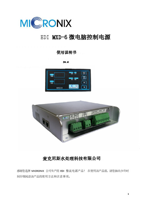
EDI MXD-6微电脑控制电源使用说明书(V6.0)麦克尼斯水处理科技有限公司感谢您选择MICRONIX 公司生产的EDI 整流电源产品!在使用该产品前,请您抽出少许时间仔细阅读该产品的使用方法和注意事项。
注意事项EDI 膜块及您选配的配套电源是属于带电工作产品,因此,在进行EDI 产品使用时,应有以下措施予以保证:1、定期检查各个接线端子的接线是否牢靠稳固。
2、处理电器故障或更换电器元件时,必须由专业的持证电气人员进行。
3、EDI 设备工作时,禁止维修或拆卸电源线。
4、不可将任何杂物、工具等物品放置在EDI 膜块上面。
5、若发生EDI 膜块渗水或泄漏情况时,应及时停止设备运行,并通知专业维护人员进行检查处理。
具体详细操作,请参见〖EDI 产品技术手册〗EDI 整流电源配置清单1、EDI整流电源膜块2、EDI显示控制器3、EDI 显示控制器紧固扣一对4、EDI 电源使用说明书概述MXD-6 是一款全新的三相整流电源控制器,使用全数字控制设计理念,使用软起动及可量化的实时控制算法,减少了模块对负载的冲击,使整个控制系统平稳可靠运行。
麦克尼斯的MXD-6 在兼容及接线方面更是友好及人性化,MXD-6 可以使用在两相及三相的环境下,无需做任何更改,三相不分接线相序,两相输入不分接线的输入端口。
MXD-6的电源模块与显示模块的连接更是简便,只需一条网线对接即可。
产品特点◆全铝合金外壳设计,经久耐用◆结构紧凑合理,接线简单,安装调试方便◆抗干扰能力强,适用各种复杂的工作环境◆电流、电压实时显示◆无冲击软启动功能◆超低待机功耗1.5W以下◆超宽工作电压◆全按键式操作,即可以在控制面板上通过按键切换恒压、恒流模式◆三相不分相序,两线不分接口◆立体散热,带载能力强一、操作及控制特点1、设置模式为全按键操作模式,即从恒流或恒压控制模式切换到恒压或恒流控制模式时,只需在面板上操作即可,无需打开电柜与机箱进行跳线选择。
美信深耕模拟市场 热门模数转换器(ADC)集锦

美信深耕模拟市场热门模数转换器(ADC)集锦
Maxim Integrated Products (美信公司)成立于1983年,以不断创造高品质的模拟工程解决方案为使命,在世界范围内为基于微处理器的电子产品客户提供增值服务。
在过去的23年里美信深耕模拟领域,开发并在市场上销售的IC超过5,400种―多于任何其他模拟半导体厂商,其中80%的产品由公司的设计工程师研发,针对美信在模拟半导体行业的影响,电子发烧友网细数了美信公司近月来推出的热门模数转换器(ADC),帮助工程师选取适合自己的解决方案。
MAX1302/MAX1303多量程、低功耗、16位、逐次逼近型模数转换器(ADC)
MAX1302/MAX1303多量程、低功耗、16位、逐次逼近型模数转换器(ADC),采用+5V单电源供电,具有高达115ksps的吞吐量。
独立的数字电源允许通过SPI™/QSPI™/MICROWIRE™兼容的串行接口与2.7V至5.25V系统连接。
局部关断模式可将电源电流降至1.3mA (典型值)。
完全关断模式则可将电源电流进一步降至1µA (典型值)。
MAX1302提供8路(单端)或4路(真差分)模拟输入通道。
MAX1303。
基于美信MAX16836多颗高亮LED驱动设计方案
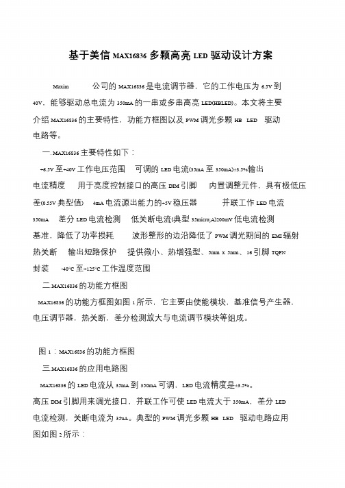
基于美信MAX16836多颗高亮LED驱动设计方案
Maxim 公司的MAX16836 是电流调节器,它的工作电压为6.5V 到40V,能够驱动总电流为350mA 的一串或多串高亮LED(HBLED)。
本文将主要介绍MAX16836 的主要特性,功能方框图以及PWM 调光多颗HB LED 驱动电路等。
一. MAX16836 主要特性如下:
+6.5V 至+40V 工作电压范围可调的LED 电流(35mA 至350mA)±3.5%输出电流精度用于亮度控制接口的高压DIM 引脚内置调整元件,具有极低压差(0.55V 典型值) 4mA 电流源出能力的+5V 稳压器并联工作LED 电流350mA 差分LED 电流检测低关断电流(典型35micro;A)200mV 低电流检测基准,降低了功率损耗波形整形的边沿降低了PWM 调光期间的EMI 辐射热关断输出短路保护提供微小、热增强型、5mm x 5mm、16 引脚TQFN 封装-40°C至+125°C工作温度范围
二.MAX16836 的功能方框图
MAX16836 的功能方框图如图1 所示,它主要由使能模块,基准信号产生器,电压调节器,热关断,差分检测放大与电流调节模块等组成。
图1:MAX16836 的功能方框图
三.MAX16836 的应用电路图
MAX16836 的LED 电流从35mA 到350mA 可调,LED 电流精度是±3.5%。
高压DIM 引脚用来调光接口,并联工作可使LED 电流大于350mA,差分LED 电流检测,关断电流为35uA。
典型的PWM 调光多颗HB LED 驱动电路应用图如图2 所示:。
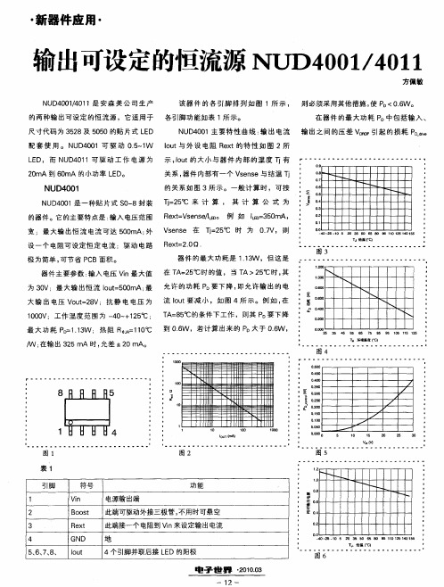
输出可设定的恒流源NUD4001/4011
柏 — 一’ 5 2 35 5 65 8 95 25 0 0 o o 11 12 1 1 0 5 40 55
T .结温 ( J 。 c)
5 6 7 8 、、、 、
Iu ot
4个引脚 并联后接 L D的阳极 E
图6
屯子 世 界
—
.0 O0 21. 3
1 一 2
尺寸代码 为 3 2 5 8及 5 5 0 0的贴 片 式 L D E
N D 0 1主要特 性 曲线 : 出 电流 输 出之 间的压 差 VRP U 40 输 。 引起 的损耗 P 。
配 套 使 用 。 N D 0 1可 驱 动 O5 1 lu U 40 .~ W o t与外 设 电阻 R x e t的特 性如 图 2所
・
新器 件应 用 ・
输出可设定的恒流源 NUD4 0 / 0 0 4 1 1 1
方佩敏 N D 0 1 0 1是安 森 美 公 司生 产 U 4 0/ 1 4 该器 件 的各 引脚排 列 如 图 1所 示 , 则 必 须 采 用 其 他 措 施 , P <06 。 使 。 .W 在 器件 的最大 功耗 P 中包括 输 入、 。 的两种输 出可设定 的恒流 源 ,它适 用于 各 引 脚 功 能 如 表 1 示 。 所
, 1 O
£ l
>
— 鬟霄 u M) d
( \ d M ) Ⅱ
\
毒6 脚 枷 毒 .W o大于{ .W , 御 |25 脚5 0 咖 最 大 功 耗 P : .3 ; 热 阻 R j 1 0 D 11 W A 1 ℃ 到 06 ,若 计算 出来 的 P e= 3 / : 输出 3 5mA时 , W 在 2 允差 ±2 。 0mA
联 1 L D的实例 如图 7所示 ,其计算 W E
MAX系列芯片大全

MAXIM/DALLAS 中文数据资料DS12CR887, DS12R885, DS12R887 RTC,带有恒压涓流充电器DS1870 LDMOS RF功放偏置控制器DS1921L-F5X Thermochron iButtonDS1923 温度/湿度记录仪iButton,具有8kB数据记录存储器DS1982, DS1982-F3, DS1982-F5 1k位只添加iButton?DS1990A 序列号iButtonDS1990R, DS1990R-F3, DS1990R-F5 序列号iButtonDS1991 多密钥iButtonDS2129 LVD SCSI 27线调节器DS2401 硅序列号DS2406 双通道、可编址开关与1k位存储器DS2408 1-Wire、8通道、可编址开关DS2411 硅序列号,带有VCC输入DS2413 1-Wire双通道、可编址开关DS2430A 256位1-Wire EEPROMDS2431 1024位、1-Wire EEPROMDS2480B 串行、1-Wire线驱动器,带有负荷检测DS2482-100 单通道1-Wire主控制器DS2482-100 勘误表PDF: 2482-100A2DS2482-800, DS2482S-800 八通道1-Wire主控制器DS2482-800 勘误表PDF: 2482-800A2DS2502 1k位只添加存储器DS2505 16k位只添加存储器DS28E04-100 4096位、可寻址、1-Wire EEPROM,带有PIODS3170DK DS3/E3单芯片收发器开发板DS3231, DS3231S 高精度、I2C集成RTC/TCXO/晶振DS33Z44 四路以太网映射器DS3902 双路、非易失、可变电阻器,带有用户EEPROMDS3906 三路、非易失、小步长调节可变电阻与存储器DS3984 4路冷阴极荧光灯控制器DS4302 2线、5位DAC,提供三路数字输出DS80C400-KIT DS80C400评估套件DS80C410, DS80C411 具有以太网和CAN接口的网络微控制器DS80C410 勘误表PDF: 80C410A1DS89C430, DS89C440, DS89C450 超高速闪存微控制器DS89C430 勘误表PDF: 89C430A2DS89C440 勘误表PDF: 89C440A2DS89C450 勘误表PDF: 89C450A2DS89C430 勘误表PDF: 89C430A3DS89C440 勘误表PDF: 89C440A3DS89C450 勘误表PDF: 89C450A3DS89C430 勘误表PDF: 89C430A5DS89C440 勘误表PDF: 89C440A5DS89C450 勘误表PDF: 89C450A5DS9090K 1-Wire器件评估板, B版DS9097U-009, DS9097U-E25, DS9097U-S09 通用1-Wire COM端口适配器DS9490, DS9490B, DS9490R USB至1-Wire/iButton适配器MAX1034, MAX1035 8/4通道、±VREF多量程输入、串行14位ADCMAX1072, MAX1075 1.8Msps、单电源、低功耗、真差分、10位ADCMAX1076, MAX1078 1.8Msps、单电源供电、低功耗、真差分、10位ADC,内置电压基准MAX1146, MAX1147, MAX1148, MAX1149 多通道、真差分、串行、14位ADCMAX1149EVKIT MAX1149评估板/评估系统MAX1220, MAX1257, MAX1258 12位、多通道ADC/DAC,带有FIFO、温度传感器和GPIO端口MAX1224, MAX1225 1.5Msps、单电源、低功耗、真差分、12位ADCMAX1258EVKIT MAX1057, MAX1058, MAX1257, MAX1258评估板/评估系统MAX1274, MAX1275 1.8Msps、单电源、低功耗、真差分、12位ADCMAX13000E, MAX13001E, MAX13002E, MAX13003E, MAX13004E, MAX13005E 超低电压电平转换器MAX1302, MAX1303 8/4通道、±VREF多量程输入、串行16位ADCMAX1304, MAX1305, MAX1306, MAX1308, MAX1309, MAX1310, MAX1312, MAX1313,MAX1314 8/4/2通道、12位、同时采样ADC,提供±10V、±5V或0至+5V模拟输入范围MAX13050, MAX13052, MAX13053, MAX13054 工业标准高速CAN收发器,具有±80V故障保护MAX13080E, MAX13081E, MAX13082E, MAX13083E, MAX13084E, MAX13085E, MAX13086E, MAX13087E, MAX13088E, MAX13089E +5.0V、±15kV ESD保护、失效保护、热插拔、RS-485/RS-422收发器MAX13101E, MAX13102E, MAX13103E, MAX13108E 16通道、带有缓冲的CMOS逻辑电平转换器MAX1334, MAX1335 4.5Msps/4Msps、5V/3V、双通道、真差分10位ADCMAX1336, MAX1337 6.5Msps/5.5Msps、5V/3V、双通道、真差分8位ADCMAX13481E, MAX13482E, MAX13483E ±15kV ESD保护USB收发器, 外部/内部上拉电阻MAX1350, MAX1351, MAX1352, MAX1353, MAX1354, MAX1355, MAX1356, MAX1357 双路、高端、电流检测放大器和驱动放大器MAX1450 低成本、1%精确度信号调理器,用于压阻式传感器MAX1452 低成本、精密的传感器信号调理器MAX1487, MAX481, MAX483, MAX485, MAX487, MAX488, MAX489, MAX490, MAX491 低功耗、限摆率、RS-485/RS-422收发器MAX1492, MAX1494 3位半和4位半、单片ADC,带有LCD驱动器MAX1494EVKIT MAX1493, MAX1494, MAX1495评估板/评估系统MAX1497, MAX1499 3位半和4位半、单片ADC,带有LED驱动器和μC接口MAX1499EVKIT MAX1499评估板/评估系统MAX15000, MAX15001 电流模式PWM控制器, 可调节开关频率MAX1515 低电压、内置开关、降压/DDR调节器MAX1518B TFT-LCD DC-DC转换器, 带有运算放大器MAX1533, MAX1537 高效率、5路输出、主电源控制器,用于笔记本电脑MAX1533EVKIT MAX1533评估板MAX1540A, MAX1541 双路降压型控制器,带有电感饱和保护、动态输出和线性稳压器MAX1540EVKIT MAX1540评估板MAX1551, MAX1555 SOT23、双输入、USB/AC适配器、单节Li+电池充电器MAX1553, MAX1554 高效率、40V、升压变换器,用于2至10个白光LED驱动MAX1556, MAX1557 16μA IQ、1.2A PWM降压型DC-DC转换器MAX1556EVKIT MAX1556EVKIT评估板MAX1558, MAX1558H 双路、3mm x 3mm、1.2A/可编程电流USB开关,带有自动复位功能MAX1586A, MAX1586B, MAX1586C, MAX1587A, MAX1587C 高效率、低IQ、带有动态内核的PMIC,用于PDA和智能电话MAX16801A/B, MAX16802A/B 离线式、DC-DC PWM控制器, 用于高亮度LED驱动器MAX1858A, MAX1875A, MAX1876A 双路180°异相工作的降压控制器,具有排序/预偏置启动和POR MAX1870A 升/降压Li+电池充电器MAX1870AEVKIT MAX1870A评估板MAX1874 双路输入、USB/AC适配器、1节Li+充电器,带OVP与温度调节MAX1954A 低成本、电流模式PWM降压控制器,带有折返式限流MAX1954AEVKIT MAX1954A评估板MAX19700 7.5Msps、超低功耗模拟前端MAX19700EVKIT MAX19700评估板/评估系统MAX19705 10位、7.5Msps、超低功耗模拟前端MAX19706 10位、22Msps、超低功耗模拟前端MAX19707 10位、45Msps、超低功耗模拟前端MAX19708 10位、11Msps、超低功耗模拟前端MAX2041 高线性度、1700MHz至3000MHz上变频/下变频混频器,带有LO缓冲器/开关MAX2043 1700MHz至3000MHz高线性度、低LO泄漏、基站Rx/Tx混频器MAX220, MAX222, MAX223, MAX225, MAX230, MAX231, MAX232, MAX232A, MAX233,MAX233A, MAX234, MAX235, MAX236, MAX237, MAX238, MAX239, MAX240, MAX241,MAX242, MAX243, MAX244, MAX245, MAX246, MAX247, MAX248, MAX249 +5V供电、多通道RS-232驱动器/接收器MAX2335 450MHz CDMA/OFDM LNA/混频器MAX2370 完备的、450MHz正交发送器MAX2370EVKIT MAX2370评估板MAX2980 电力线通信模拟前端收发器MAX2986 集成电力线数字收发器MAX3013 +1.2V至+3.6V、0.1μA、100Mbps、8路电平转换器MAX3205E, MAX3207E, MAX3208E 双路、四路、六路高速差分ESD保护ICMAX3301E, MAX3302E USB On-the-Go收发器与电荷泵MAX3344E, MAX3345E ±15kV ESD保护、USB收发器,UCSP封装,带有USB检测MAX3394E, MAX3395E, MAX3396E ±15kV ESD保护、大电流驱动、双/四/八通道电平转换器, 带有加速电路MAX3535E, MXL1535E +3V至+5V、提供2500VRMS隔离的RS-485/RS-422收发器,带有±15kV ESD保护MAX3570, MAX3571, MAX3573 HI-IF单芯片宽带调谐器MAX3643EVKIT MAX3643评估板MAX3645 +2.97V至+5.5V、125Mbps至200Mbps限幅放大器,带有信号丢失检测器MAX3645EVKIT MAX3645评估板MAX3654 47MHz至870MHz模拟CATV互阻放大器MAX3654EVKIT MAX3654评估板MAX3657 155Mbps低噪声互阻放大器MAX3658 622Mbps、低噪声、高增益互阻前置放大器MAX3735, MAX3735A 2.7Gbps、低功耗、SFP激光驱动器MAX3737 多速率激光驱动器,带有消光比控制MAX3737EVKIT MAX3737评估板MAX3738 155Mbps至2.7Gbps SFF/SFP激光驱动器,带有消光比控制MAX3744, MAX3745 2.7Gbps SFP互阻放大器,带有RSSIMAX3744EVKIT, MAX3745EVKIT MAX3744, MAX3745评估板MAX3748, MAX3748A, MAX3748B 紧凑的、155Mbps至4.25Gbps限幅放大器MAX3785 6.25Gbps、1.8V PC板均衡器MAX3787EVKIT MAX3787评估板MAX3793 1Gbps至4.25Gbps多速率互阻放大器,具有光电流监视器MAX3793EVKIT MAX3793评估板MAX3805 10.7Gbps自适应接收均衡器MAX3805EVKIT MAX3805评估板MAX3840 +3.3V、2.7Gbps双路2 x 2交叉点开关MAX3841 12.5Gbps CML 2 x 2交叉点开关MAX3967 270Mbps SFP LED驱动器MAX3969 200Mbps SFP限幅放大器MAX3969EVKIT MAX3969评估板MAX3982 SFP铜缆预加重驱动器MAX3983 四路铜缆信号调理器MAX3983EVKIT MAX3983评估板MAX3983SMAEVKIT MAX3983 SMA连接器评估板MAX4079 完备的音频/视频后端方案MAX4079EVKIT MAX4079评估板MAX4210, MAX4211 高端功率、电流监视器MAX4210EEVKIT MAX4210E、MAX4210A/B/C/D/F评估板MAX4211EEVKIT MAX4211A/B/C/D/E/F评估板MAX4397 用于双SCART连接器的音频/视频开关MAX4397EVKIT MAX4397评估系统/评估板MAX4411EVKIT MAX4411评估板MAX4729, MAX4730 低电压、3.5、SPDT、CMOS模拟开关MAX4754, MAX4755, MAX4756 0.5、四路SPDT开关,UCSP/QFN封装MAX4758, MAX4759 四路DPDT音频/数据开关,UCSP/QFN封装MAX4760, MAX4761 宽带、四路DPDT开关MAX4766 0.075A至1.5A、可编程限流开关MAX4772, MAX4773 200mA/500mA可选的限流开关MAX4795, MAX4796, MAX4797, MAX4798 450mA/500mA限流开关MAX4826, MAX4827, MAX4828, MAX4829, MAX4830, MAX4831 50mA/100mA限流开关, 带有空载标记, μDFN封装MAX4832, MAX4833 100mA LDO,带有限流开关MAX4834, MAX4835 250mA LDO,带有限流开关MAX4836, MAX4837 500mA LDO,带有限流开关MAX4838A, MAX4840A, MAX4842A 过压保护控制器,带有状态指示FLAGMAX4850, MAX4850H, MAX4852, MAX4852H 双路SPDT模拟开关,可处理超摆幅信号MAX4851, MAX4851H, MAX4853, MAX4853H 3.5/7四路SPST模拟开关,可处理超摆幅信号MAX4854 7四路SPST模拟开关,可处理超摆幅信号MAX4854H, MAX4854HL 四路SPST、宽带、信号线保护开关MAX4855 0.75、双路SPDT音频开关,具有集成比较器MAX4864L, MAX4865L, MAX4866L, MAX4867, MAX4865, MAX4866 过压保护控制器,具有反向保护功能MAX4880 过压保护控制器, 内置断路开关MAX4881, MAX4882, MAX4883, MAX4884 过压保护控制器, 内部限流, TDFN封装MAX4901, MAX4902, MAX4903, MAX4904, MAX4905 低RON、双路SPST/单路SPDT、无杂音切换开关, 可处理负电压MAX4906, MAX4906F, MAX4907, MAX4907F 高速/全速USB 2.0开关MAX5033 500mA、76V、高效率、MAXPower降压型DC-DC变换器MAX5042, MAX5043 双路开关电源IC,集成了功率MOSFET和热插拔控制器MAX5058, MAX5059 可并联的副边同步整流驱动器和反馈发生器控制ICMAX5058EVKIT MAX5051, MAX5058评估板MAX5062, MAX5062A, MAX5063, MAX5063A, MAX5064, MAX5064A, MAX5064B 125V/2A、高速、半桥MOSFET驱动器MAX5065, MAX5067 双相、+0.6V至+3.3V输出可并联、平均电流模式控制器MAX5070, MAX5071 高性能、单端、电流模式PWM控制器MAX5072 2.2MHz、双输出、降压或升压型转换器,带有POR和电源失效输出MAX5072EVKIT MAX5072评估板MAX5074 内置MOSFET的电源IC,用于隔离型IEEE 802.3af PD和电信电源MAX5078 4A、20ns、MOSFET驱动器MAX5084, MAX5085 65V、200mA、低静态电流线性稳压器, TDFN封装MAX5088, MAX5089 2.2MHz、2A降压型转换器, 内置高边开关MAX5094A, MAX5094B, MAX5094C, MAX5094D, MAX5095A, MAX5095B, MAX5095C 高性能、单端、电流模式PWM控制器MAX5128 128抽头、非易失、线性变化数字电位器, 采用2mm x 2mm μDFN封装MAX5417, MAX5417L, MAX5417M, MAX5417N, MAX5417P, MAX5418, MAX5419 256抽头、非易失、I2C接口、数字电位器MAX5417LEVKIT MAX5417_, MAX5418_, MAX5419_评估板/评估系统MAX5477, MAX5478, MAX5479 双路、256抽头、非易失、I2C接口、数字电位器MAX5478EVKIT MAX5477/MAX5478/MAX5479评估板/评估系统MAX5490 100k精密匹配的电阻分压器,SOT23封装MAX5527, MAX5528, MAX5529 64抽头、一次性编程、线性调节数字电位器MAX5820 双路、8位、低功耗、2线、串行电压输出DACMAX5865 超低功耗、高动态性能、40Msps模拟前端MAX5920 -48V热插拔控制器,外置RsenseMAX5921, MAX5939 -48V热插拔控制器,外置Rsense、提供较高的栅极下拉电流MAX5932 正电源、高压、热插拔控制器MAX5932EVKIT MAX5932评估板MAX5936, MAX5937 -48V热插拔控制器,可避免VIN阶跃故障,无需RSENSEMAX5940A, MAX5940B IEEE 802.3af PD接口控制器,用于以太网供电MAX5940BEVKIT MAX5940B, MAX5940D评估板MAX5941A, MAX5941B 符合IEEE 802.3af标准的以太网供电接口/PWM控制器,适用于用电设备MAX5945 四路网络电源控制器,用于网络供电MAX5945EVKIT, MAX5945EVSYS MAX5945评估板/评估系统MAX5953A, MAX5953B, MAX5953C, MAX5953D IEEE 802.3af PD接口和PWM控制器,集成功率MOSFETMAX6640 2通道温度监视器,提供双路、自动PWM风扇速度控制器MAX6640EVKIT MAX6640评估系统/评估板MAX6641 兼容于SMBus的温度监视器,带有自动PWM风扇速度控制器MAX6643, MAX6644, MAX6645 自动PWM风扇速度控制器,带有过温报警输出MAX6678 2通道温度监视器,提供双路、自动PWM风扇速度控制器和5个GPIOMAX6695, MAX6696 双路远端/本地温度传感器,带有SMBus串行接口MAX6877EVKIT MAX6877评估板MAX6950, MAX6951 串行接口、+2.7V至+5.5V、5位或8位LED显示驱动器MAX6966, MAX6967 10端口、恒流LED驱动器和输入/输出扩展器,带有PWM亮度控制MAX6968 8端口、5.5V恒流LED驱动器MAX6969 16端口、5.5V恒流LED驱动器MAX6970 8端口、36V恒流LED驱动器MAX6977 8端口、5.5V恒流LED驱动器,带有LED故障检测MAX6978 8端口、5.5V恒流LED驱动器,带有LED故障检测和看门狗MAX6980 8端口、36V恒流LED驱动器, 带有LED故障检测和看门狗MAX6981 8端口、36V恒流LED驱动器, 带有LED故障检测MAX7030 低成本、315MHz、345MHz和433.92MHz ASK收发器, 带有N分频PLLMAX7032 低成本、基于晶振的可编程ASK/FSK收发器, 带有N分频PLLMAX7317 10端口、SPI接口输入/输出扩展器,带有过压和热插入保护MAX7319 I2C端口扩展器,具有8路输入,可屏蔽瞬态检测MAX7320 I2C端口扩展器, 带有八个推挽式输出MAX7321 I2C端口扩展器,具有8个漏极开路I/O口MAX7328, MAX7329 I2C端口扩展器, 带有八个I/O口MAX7347, MAX7348, MAX7349 2线接口、低EMI键盘开关和发声控制器MAX7349EVKIT MAX7349评估板/仿真: MAX7347/MAX7348MAX7375 3引脚硅振荡器MAX7381 3引脚硅振荡器MAX7389, MAX7390 微控制器时钟发生器, 带有看门狗MAX7391 快速切换时钟发生器, 带有电源失效检测MAX7445 4通道视频重建滤波器MAX7450, MAX7451, MAX7452 视频信号调理器,带有AGC和后肩钳位MAX7452EVKIT MAX7452评估板MAX7462, MAX7463 单通道视频重建滤波器和缓冲器MAX8505 3A、1MHz、1%精确度、内置开关的降压型调节器,带有电源就绪指示MAX8524, MAX8525 2至8相VRM 10/9.1 PWM控制器,提供精密的电流分配和快速电压定位MAX8525EVKIT MAX8523, MAX8525评估板MAX8533 更小、更可靠的12V、Infiniband兼容热插拔控制器MAX8533EVKIT MAX8533评估板MAX8545, MAX8546, MAX8548 低成本、宽输入范围、降压控制器,带有折返式限流MAX8550, MAX8551 集成DDR电源方案,适用于台式机、笔记本电脑及图形卡MAX8550EVKIT MAX8550, MAX8550A, MAX8551评估板MAX8552 高速、宽输入范围、单相MOSFET驱动器MAX8553, MAX8554 4.5V至28V输入、同步PWM降压控制器,适合DDR端接和负载点应用MAX8563, MAX8564 ±1%、超低输出电压、双路或三路线性n-FET控制器MAX8564EVKIT MAX8563, MAX8564评估板MAX8566 高效、10A、PWM降压调节器, 内置开关MAX8570, MAX8571, MAX8572, MAX8573, MAX8574, MAX8575 高效LCD升压电路,可True ShutdownMAX8571EVKIT MAX8570, MAX8571, MAX8572, MAX8573, MAX8574, MAX8575评估板MAX8576, MAX8577, MAX8578, MAX8579 3V至28V输入、低成本、迟滞同步降压控制器MAX8594, MAX8594A 5路输出PMIC,提供DC-DC核电源,用于低成本PDAMAX8594EVKIT MAX8594评估板MAX8632 集成DDR电源方案,适用于台式机、笔记本电脑和图形卡MAX8632EVKIT MAX8632评估板MAX8702, MAX8703 双相MOSFET驱动器,带有温度传感器MAX8707 多相、固定频率控制器,用于AMD Hammer CPU核电源MAX8716, MAX8717, MAX8757 交叉工作、高效、双电源控制器,用于笔记本电脑MAX8716EVKIT MAX8716评估板MAX8717EVKIT MAX8717评估板MAX8718, MAX8719 高压、低功耗线性稳压器,用于笔记本电脑MAX8725EVKIT MAX8725评估板MAX8727 TFT-LCD升压型、DC-DC变换器MAX8727EVKIT MAX8727评估板MAX8729 固定频率、半桥CCFL逆变控制器MAX8729EVKIT MAX8729评估板MAX8732A, MAX8733A, MAX8734A 高效率、四路输出、主电源控制器,用于笔记本电脑MAX8737 双路、低电压线性稳压器, 外置MOSFETMAX8737EVKIT MAX8737评估板MAX8738 EEPROM可编程TFT VCOM校准器, 带有I2C接口MAX8740 TFT-LCD升压型、DC-DC变换器MAX8743 双路、高效率、降压型控制器,关断状态下提供高阻MAX8751 固定频率、全桥、CCFL逆变控制器MAX8751EVKIT MAX8751评估板MAX8752 TFT-LCD升压型、DC-DC变换器MAX8758 具有开关控制和运算放大器的升压调节器, 用于TFT LCDMAX8758EVKIT MAX8758评估板MAX8759 低成本SMBus CCFL背光控制器MAX8760 双相、Quick-PWM控制器,用于AMD Mobile Turion 64 CPU核电源MAX8764 高速、降压型控制器,带有精确的限流控制,用于笔记本电脑MAX9223, MAX9224 22位、低功耗、5MHz至10MHz串行器与解串器芯片组MAX9225, MAX9226 10位、低功耗、10MHz至20MHz串行器与解串器芯片组MAX9483, MAX9484 双输出、多模CD-RW/DVD激光二极管驱动器MAX9485 可编程音频时钟发生器MAX9485EVKIT MAX9485评估板MAX9486 8kHz参考时钟合成器,提供35.328MHz倍频输出MAX9486EVKIT MAX9486评估板MAX9489 多路输出网络时钟发生器MAX9500, MAX9501 三通道HDTV滤波器MAX9500EVKIT MAX9500评估板MAX9501EVKIT MAX9501评估板MAX9502 2.5V视频放大器, 带有重建滤波器MAX9504A, MAX9504B 3V/5V、6dB视频放大器, 可提供大电流输出MAX9701 1.3W、无需滤波、立体声D类音频功率放大器MAX9701EVKIT MAX9701评估板MAX9702 1.8W、无需滤波、立体声D类音频功率放大器和DirectDrive立体声耳机放大器MAX9702EVSYS/EVKIT MAX9702/MAX9702B评估系统/评估板MAX9703, MAX9704 10W立体声/15W单声道、无需滤波的扩展频谱D类放大器MAX9705 2.3W、超低EMI、无需滤波、D类音频放大器MAX9705BEVKIT MAX9705B评估板MAX9710EVKIT MAX9710评估板MAX9712 500mW、低EMI、无需滤波、D类音频放大器MAX9713, MAX9714 6W、无需滤波、扩频单声道/立体声D类放大器MAX9714EVKIT MAX9704, MAX9714评估板MAX9715 2.8W、低EMI、立体声、无需滤波、D类音频放大器MAX9715EVKIT MAX9715评估板MAX9716, MAX9717 低成本、单声道、1.4W BTL音频功率放大器MAX9716EVKIT MAX9716评估板MAX9718, MAX9719 低成本、单声道/立体声、1.4W差分音频功率放大器MAX9718AEVKIT MAX9718A评估板MAX9719AEVKIT MAX9719A/B/C/D评估板MAX9721 1V、固定增益、DirectDrive、立体声耳机放大器,带有关断MAX9721EVKIT MAX9721评估板MAX9722A, MAX9722B 5V、差分输入、DirectDrive、130mW立体声耳机放大器,带有关断MAX9722AEVKIT MAX9722A, MAX9722B评估板MAX9723 立体声DirectDrive耳机放大器, 具有BassMax、音量控制和I2C接口MAX9725 1V、低功率、DirectDrive、立体声耳机放大器,带有关断MAX9728AEVKIT MAX9728A/MAX9728B评估板MAX9750, MAX9751, MAX9755 2.6W立体声音频功放和DirectDrive耳机放大器MAX9759 3.2W、高效、低EMI、无需滤波、D类音频放大器MAX9759EVKIT MAX9759评估板MAX9770, MAX9772 1.2W、低EMI、无需虑波、单声道D类放大器,带有立体声DirectDrive耳机放大器MAX9787 2.2W立体声音频功率放大器, 提供模拟音量控制MAX9850 立体声音频DAC,带有DirectDrive耳机放大器MAX9890 音频咔嗒声-怦然声抑制器MAX9951, MAX9952 双路引脚参数测量单元MAX9960 双闪存引脚电子测量/高压开关矩阵MAX9961, MAX9962 双通道、低功耗、500Mbps ATE驱动器/比较器,带有2mA负载MAX9967 双通道、低功耗、500Mbps ATE驱动器/比较器,带有35mA负载MAX9986A SiGe高线性度、815MHz至1000MHz下变频混频器, 带有LO缓冲器/开关MAXQ2000 低功耗LCD微控制器MAXQ2000 勘误表PDF: MAXQ2000A2MAXQ2000-KIT MAXQ2000评估板MAXQ3120-KIT MAXQ3120评估板MXL1543B +5V、多协议、3Tx/3Rx、软件可选的时钟/数据收发器。
电子工程师常用的10款稳压元件
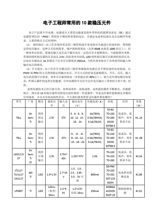
电子工程师常用的10款稳压元件电子产品离不开电源,电源部分主要的功能就是将外界供给的抵押直流电(DC)通过电源管理区间(PMIC)得到各个期间所需要的电压,并满足电流和纹波以及启动顺序等要求。
主要的稳压方式有两种:(1)线性稳压 - 由工作在线性状态的三极管构成可变电阻对负载进行恒流控制,得到稳定的电压输出。
这种方式结构简单、噪声抑制度很高(达到60dB也就是1000倍以上),但一般效率比较低,要满足输入电压高于输出电压一定的压差才能够稳压,只能做降压变换。
常规的线性稳压器的压差高达2.5V,因此效率比较低,LDO线性稳压器可以做到较低的压差,比如在负载高达1A的情况下压差可以降低到350mA,当然其效率取决于具体使用的输入和输出电压的情况。
(2)开关稳压 - 由工作在开关模式的三极管和储能的电感以及平滑纹波的电容构成,以PWM或PFM的方式得到稳定的输出电压。
开关方式的好处是能够降压、升压、反压,输入电压的范围可以很宽,效率可以做到很高(有的能达到95%以上),缺点是外围电路比较复杂,外围元器件的选型比较敏感,另外高频的开关信号会在电压输出上带来较大的干扰、纹波。
虽然电源技术已经日新月异,各种高效率、高集成度、高性能的器件不断推出,但根据统计,排在前10的稳压器件仍然是比较经典的一些老器件,毕竟这些器件能够满足多数的可以看成是78xx的夫妻档,经常配对使用。
78xx得到的是对地正电压,79xx得到的是对地负电压,除此之外跟78xx一样;3.LM317/LM117上面的78xx和79xx的器件输出电压是固定的,不可调整,LM317则是输出电压可以调节的线性稳压器,也有不同的封装支持不同的电流输出,最大输出电路可以高达 1.5A;也要求2.5v以上的压差才能正常稳压工作,也具备78xx一样的优点和缺点;4. 1117系列非常经典的LDO线性稳压器,相比于78xx和LM317系列的器件,它要求的输入电压和输出电压的差值为1.2V,因此可以广泛用在电池供电的便携式系统里面,比如通过4节1.25V 的电池(满电量的时候达到5V),电量不足到4.5V电压的时候依然能够通过1117-3.3得到3.3V的稳压输出供板子上的3.3V电路工作。
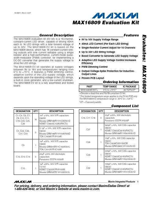
MAX16809EVKIT+中文资料
General DescriptionThe MAX16809 evaluation kit (EV kit) is a 16-channel,constant-current LED driver, capable of driving 40mA each to 16 LED strings with a total forward voltage of up to 32V. The MAX16809 EV kit is based on the MAX16809 device, which has 16 constant-current-sink-ing outputs with sink current settable using a single resistor and a high-performance, current-mode pulse-width-modulator (PWM) controller, for implementing a DC-DC converter that generates the supply voltage to drive the LED strings.The MAX16809 EV kit operates at supply voltages between 9V to 16V and temperatures ranging from 0°C to +70°C. I t features a PWM dimming control,adaptive control of the LED supply voltage, which depends upon the operating voltage of the LED strings,a built-in clock generator, and a low-current shutdown.The MAX16809 EV kit is a fully assembled and tested board.Features♦9V to 16V Supply Voltage Range♦40mA LED Current (Per Each LED String)♦Single-Resistor Current Adjust for 16 Channels ♦Up to 32V LED String Voltage♦Boost Converter to Generate LED Supply Voltage ♦Adaptive LED Supply Voltage Control Increases Efficiency ♦PWM Dimming Control♦Output-Voltage-Spike Protection for Inductive-Output Lines ♦Proven PCB LayoutEvaluates: MAX16809MAX16809 Evaluation Kit________________________________________________________________Maxim Integrated Products 119-0821; Rev 0; 5/07For pricing, delivery, and ordering information,please contact Maxim/Dallas Direct!at 1-888-629-4642, or visit Maxim’s website at .Ordering Information*This limited temperature range applies to the EV kit PCB only.The MAX16809 IC temperature range is -40°C to +125°C.†EP = Exposed paddle.E v a l u a t e s : M A X 16809MAX16809 Evaluation Kit 2_______________________________________________________________________________________Evaluates: MAX16809MAX16809 Evaluation Kit_______________________________________________________________________________________3Quick StartRecommended Equipment•One 16V, 5A adjustable power supply •One 5V power supply•16 LED strings with a total forward voltage ≤32V •One multimeter•One PWM signal generator (optional)ProcedureThe MAX16809 EV kit is fully assembled and tested.Follow the steps below to verify operation. Caution: Do not turn on the power supply until all connections are completed.1)Connect LED strings with operating voltage ofapproximately 32V between VLED (pins 1-4 of J1)and OUT0–OUT15 (pins 5-20 of J1). All 16 channels should have an LED string load connected of the same type.2)Connect the DC power supply (16V, 5A) to VIN andGND.3)Connect a DC power supply (0 to 5V) to VBIAS andGND.4)Turn on the power supplies and apply 10V to VI Nand 3V to 5V to VBIAS. Connect SHDN and PWM to 3V to 5V. All of the LEDs should turn on. Measure the current through any LED string, which should be 40mA ±7%.5)I ncrease the supply voltage to 16V and the LEDcurrents will be stable. Measure the current through any LED string, which should be 40mA ±7%.6)Apply a PWM signal with amplitude of 3V to 5V anda frequency between 100Hz and 2kHz to the PWM input. The LED brightness should increase as the PWM duty cycle increases and viceversa.7)Connect SHDN to GND and all LEDs should turn off.Detailed DescriptionThe MAX16809 EV kit is a 16-channel, constant-current LED driver capable of driving 40mA each to 16 LED strings, with a total forward voltage of up to 32V. The MAX16809 EV kit can drive a total of 160 white LEDs in 16 strings, with operating current up to 40mA. The MAX16809 EV kit can operate at input supply voltages between 9V and 16V.The MAX16809 EV kit evaluates the MAX16809 IC, which has two major sections. The first section consists of 16constant-current LED drivers capable of sinking up to 55mA when on and blocking up to 36V when off. The sec-ond section is a high-performance current-mode PWMcontroller that can control a DC-DC converter to generate the supply voltage for driving the LED strings. The MAX16809 EV kit uses the PWM controller to drive a boost converter, which takes a 9V to 16V input and gen-erates a 33V LED supply voltage. To drive a constant cur-rent into an LED string, connect the LED string between the 33V output and any of the 16 constant-current-sink outputs. The resistor (R1) from the SET pin to ground pro-grams the sink current of each output. The sink current of any output can be up to 55mA and the amplitude is the same value for all the outputs. The difference between the total forward voltage and the LED supply voltage drops between the constant-current-sink output and ground,and is dissipated as power in the device.The LED supply voltage generated by the boost con-verter in the MAX16809 EV kit is adaptive. The LED string with the highest total forward voltage dominates the control loop, and the boost-converter voltage is adjusted so that the driver associated with that string receives just enough voltage required for current drive.All the other strings, with lower total forward voltages,will have excess supply voltage, which is then dropped in the associated driver. This feedback mechanism ensures that the linear-current-control circuit dissipates the minimum possible power. An on-board inverter (U4A) is configured to generate the clock input for the MAX16809. The constant-current output-driver circuits and U4 need a 3.3V to 5V input, which should be sup-plied externally. If 5V is not available, it can be generat-ed using an emitter-follower buffer from the REF output of MAX16809.Boost ConverterThe boost converter that generates the 33V LED supply voltage operates at a switching frequency of 350kHz in continuous-conduction mode (CCM). The current-mode PWM controller in the MAX16809 drives the external MOSFET (Q2) to control the boost converter. The MOSFET is turned on at the beginning of every switching cycle and turned off when the current through the induc-tor (L1) reaches the peak value set by the error-amplifier-output voltage. Inductor current is sensed from the volt-age across the ground-referenced current-sense resis-tor (parallel combination of R12 and R13). This current-sense information is passed on to the current-sense comparators in the MAX16809 through the CS pin.During the on period of the MOSFET, the inductor stores energy from the input supply. When the switch is turned off, the inductor generates sufficient voltage in reverse direction to discharge the stored energy to VLED. This generated voltage forms a source, in series with the input supply voltage, and drives VLED through the rectifier diode (D2).E v a l u a t e s : M A X 16809MAX16809 Evaluation Kit4_______________________________________________________________________________________As the boost converter is operated in CCM, only part of the stored energy in the inductor is discharged to VLED.The advantages of CCM include reduced input and out-put filtering, reduced EMI due to lower peak currents,and higher converter efficiency. However, these advan-tages come at the cost of a right-half-plane zero in the converter-transfer function. Compensating this zero requires reducing the system bandwidth, which affects the converter-dynamic response. As the 16-channel,constant-current-sink outputs control the current through the LEDs, slower control of VLED does not affect the LED operation. Compensation of the feedback circuit is explained in the Feedback Compensation section.An internal comparator turns off the gate pulse to the external MOSFET if the voltage at the CS pin exceeds 0.3V. The current through the inductor that produces 0.3V at the CS pin is the maximum inductor current possible (the actual current can be a little higher than this limit due to the 60ns propagation delay from the CS pin to the MOSFET drive output). This condition can happen when the feedback loop is broken, when the output capacitor charges during power-up, or when there is an overload at the output. This feature protects the MOSFET by limiting the maximum current passing through it during such conditions.The RC filter, consisting of R9 and C10, removes the voltage spike across the current-sense resistors pro-duced by the turn-on gate current of the MOSFET and the reverse-recovery current of D2. Without filtering,these current spikes can cause sense comparators to falsely trigger and turn off the gate pulse prematurely.The filter time constant should not be higher than required (the MAX16809 EV kit uses a 120ns time con-stant), as a higher time constant adds additional delay to the current-sense voltage, effectively increasing the current limit.During normal operating conditions, the feedback loop controls the peak current. The error amplifier compares a scaled-down version of the LED supply voltage (VLED) with a highly accurate 2.5V reference. The error amplifier and compensation network then amplify the error signal, and the current comparator compares this signal to the sensed-current voltage to create a PWM drive output.Power-Circuit DesignI nitially, decide the input supply voltage range, output voltage VLED (the sum of the maximum LED total for-ward voltage and 1V bias voltage for the constant-cur-rent-sink output), and the output current I OUT (the sum of all the LED string currents).Calculate maximum duty cycle D MAX using the following equation:where V D is the forward drop of the rectifier diode D2(~0.6V), VIN MIN is the minimum input supply voltage (in this case, 9V), and V FET is the average drain-to-source voltage of the MOSFET Q2 when it is on.Select the switching frequency F SW based on the space, noise, dynamic response, and efficiency con-straints. Select the maximum peak-to-peak ripple on the inductor current I L PP . For the MAX16809 EV kit,F SW is 350kHz and IL PP is ±30% of the average induc-tor current. Use the following equations to calculate the maximum average-inductor current I L AVG and peak inductor current IL PEAK :Since I L PP is ±30% of the average-inductor current ILAVG :Calculate the minimum inductance value L MIN with the inductor current ripple set to the maximum value:Choose an inductor that has a minimum inductance greater than this calculated value.Calculate the current-sense resistor (R12 in parallel with R13) using the equation below:where 0.3V is the maximum current-sense signal volt-age. The factor 0.75 is for compensating the reduction of maximum current-sense voltage due to the additionof slope compensation. Check this factor and adjust after the slope compensation is calculated. See the Slope Compensation section for more information.IL IL PP AVG =××032.Evaluates: MAX16809MAX16809 Evaluation Kit_______________________________________________________________________________________5The saturation current limit of the selected inductor (IL SAT ) should be greater than the value given by the equation below. Selecting an inductor with 10% higher IL SAT rating is a good choice:Calculate the output capacitor C OUT (parallel combina-tion of C16, C17, C18, and C24) using the followingequation:where VLED PP is the peak-to-peak ripple in the LED supply voltage. The value of the calculated output capacitance will be much lower than what is actually necessary for feedback loop compensation. See the Feedback Compensation section to calculate the out-put capacitance based on the compensation require-ments.Calculate the input capacitor C IN (parallel combination of C12, C13, C14, and C5) using the following equation:where VI N PP is the peak-to-peak input ripple voltage.This equation assumes that input capacitors supply most of the input ripple current.Selection of Power SemiconductorsThe switching MOSFET (Q2) should have a voltage rat-ing sufficient to withstand the maximum output voltage,together with the diode drop of D2, and any possible overshoot due to ringing caused by parasitic induc-tances and capacitances. Use a MOSFET with voltage rating higher than that calculated by the following equation:The factor of 1.3 provides a 30% safety margin.The continuous drain-current rating of the selected MOSFET when the case temperature is at +70°C should be greater than that calculated by the following equation.The MOSFET must be mounted on a board, as per manufacturer specifications, to dissipate the heat:The MOSFET dissipates power due to both switchinglosses, as well as conduction losses. Use the following equation to calculate the conduction losses in the MOSFET:where RDS ON is the on-state drain-source resistance of the MOSFET with an assumed junction temperature of 100°C.Use the following equation to calculate the switching losses in the MOSFET:where I GON and I GOFF are the gate currents of the MOSFET (with V GS equal to the threshold voltage)when it is turned on and turned off, respectively, and C GD is the gate-to-drain MOSFET capacitance. Choose a MOSFET that has a higher power rating than that cal-culated by the following equation when the MOSFET case temperature is at +70°C:The MAX16809 EV kit uses a Schottky diode as the boost-converter rectifier (D2). A Schottky rectifier diode produces less forward drop and puts the least burden on the MOSFET during reverse recovery. If a diode with considerable reverse-recovery time is used, it should be considered in the MOSFET switching-loss calculation.The Schottky diode selected should have a voltage rat-ing 20% above the maximum boost-converter output voltage. The current rating of the diode should be greater than I Din the following equation:P P P TOT COND SW=+V VLED V DS D =+()×13.IL IL SAT PEAK=×11.E v a l u a t e s : M A X 16809MAX16809 Evaluation Kit 6_______________________________________________________________________________________Slope CompensationWhen the boost converter operates in CCM with more than 50% duty cycle, subharmonic oscillations occur if slope compensation is not implemented. Subharmonic oscillations do not allow the PWM duty cycle to settle to a peak current value set by the voltage-feedback loop.The duty cycle oscillates back and forth about the required value, usually at half the switching frequency.Subharmonic oscillations die out if a sufficient negative slope is added to the inductor peak current. This means that for any peak current set by the feedback loop, the output pulse terminates sooner than normally expected. The minimum slope compensation that should be added to stabilize the current loop is half of the worst-case (max) falling slope of inductor current.Adding a ramp to the current-sense signal, with posi-tive slope in sync with the switching frequency, can produce the desired function. The greater the duty cycle, the greater the added voltage, and the greater the difference between the set current and the actual inductor current. In the MAX16809 EV kit, the oscillator ramp signal is buffered using Q1 and added to the cur-rent-sense signal with proper scaling to implement the slope compensation. Follow the steps below to calcu-late the component values for slope compensation.Calculate the worst-case falling slope of the inductor current using the following equation:From the inductor current falling slope, find its equiva-lent voltage slope across the current-sense resistor R CS (R12 parallel with R13) using the following equation:The minimum voltage slope that should be added to the current-sense waveform is half of V SLOPE for ensur-ing stability up to 100% duty cycle. As the maximum continuous duty cycle used is less than 100%, the mini-mum required compensation slope becomes:The factor 1.1 provides a 10% margin. Resistors R9and R10 determine the attenuation of the buffered volt-age slope from the emitter of Q1. The forward drop ofsignal diode D11, together with the V BE of Q1, almost cancel the 1.1V offset of the ramp waveform. Calculate the approximate slope of the oscillator ramp using the following equation:where 1.7V is the ramp amplitude and F SW is the switching frequency.Select the value of R9 such that the input bias current of the current-sense comparators does not add consider-able error to the current-sense signal. The value of R10for the slope compensation is given by the equation:LED DriverThe MAX16809 features a 16-channel, constant-current LED driver, with each channel capable of sinking up to 55mA of LED current. The LED strings are connected between VLED and the constant-current-sink outputs to drive regulated current through LED strings. The cur-rent through all 16 channels is controlled through resis-tor (R1) from the SET pin to ground. The MAX16809 EV kit sets the current through each string at 40mA and the maximum LED supply voltage to 33V. The MAX16809EV kit drives LED strings with a total forward voltage of up to 32V.A 4-wire serial interface with four inputs (DIN, CLK, LE,and OE ) individually control the constant-current out-puts. I n the MAX16809 EV kit, a 50kHz clock signal,generated by U4A, clocks 16 1s into the internal shift register by tying DIN and LE to 5V. The clock-generation circuit can be avoided if a microcontroller provides the function.The output enable (OE ) can provide PWM dimming. An inverted PWM signal, generated by the inverter U4B, is necessary to drive the OE pin. When the PWM signal is low (LED drivers off), it also influences the feedback with the network formed by R6 and D12. See the Adaptive LED Supply Voltage Control section for more details.I f an inverted PWM signal is available, use the circuit shown in Figure1 to drive the OE input and feedbacknetwork.VR F SLOPE SW=×17.V IL R SLOPE SLOPE CS=×Evaluates: MAX16809MAX16809 Evaluation Kit_______________________________________________________________________________________7Output Current SettingThe amplitude of the output sink currents for all 16channels is set to the same value by the resistor (R1)from the SET pin to ground. The minimum allowed value of R SET is 311Ω, which sets the output currents to 55mA. The maximum allowed value of R SET is 5k Ω. The MAX16809 EV kit uses 430Ωfor R SET , which sets the output current to 40mA. To set a different output cur-rent, use the following equation:where R SET is the current-setting resistor (R1) value in ohms and I OUT is the desired output current in milliamps.Adaptive LED Supply Voltage ControlTo reduce power dissipation in the I C, the MAX16809EV kit features adaptive control of VLED based on the operating voltage of the LED strings. The constant-cur-rent-sink outputs can sink stable currents with output voltages as low as 0.8V. The voltage at each of the 16outputs will be the difference between VLED and the total forward voltage of the LED string connected to that output. The MAX16809 EV kit implements a feed-back mechanism to sense the voltage at each of the 16constant-current-sink outputs. Using dual zener diodes (D3–D10), the MAX16809 EV kit selects the lowest dri-ver voltage (with the greatest LED string voltage) to regulate. The boost-converter PWM then adjusts so that VLED is high enough for this sink output to settle toapproximately 0.8V. All the other strings have sufficient voltage, as their total forward voltages are lower. The feedback mechanism ensures that the IC dissipates the minimum possible power. For adaptive control to func-tion efficiently connect LED strings to all 16 channels and use an equal number of LEDs from the same bin in each string. I f some of the 16 channels are not used,then the zener diodes (D3–D10) should be removed from the unused channels.Use the equation below to calculate the value of R2 to get the required minimum voltage at the sink outputs:where 2.5V is the feedback reference, V DZ is the for-ward drop of the ORing diode (D3–D10), V S = 0.5V is the required sink-output voltage, and V FLED is the nom-inal total forward voltage of the LED strings. Select the value of R2 such that R7 is approximately 10k Ω.The zener diodes (D3–D10) also provide output over-voltage protection. If an LED string gets partially or fully shorted, making the sink-output voltage go high, the 15V zener diode connected to that output conducts in reverse direction, and limits the VLED voltage. Under this condition, the other LED strings might not turn on.When the outputs are off, the LED drivers are at high impedance and the feedback network now combines R6 and D12 to provide a path for the feedback currentand to control VLED. Use the following equation toE v a l u a t e s : M A X 16809MAX16809 Evaluation Kit 8_______________________________________________________________________________________calculate the value of R6 to get the required LED sup-ply voltage during PWM off time:where 2.5V is the feedback-reference voltage, 0.4V is the total voltage dropped by D4 and PWM input, and VLED OFF is the desired LED supply voltage during PWM off time. VLED OFF should be set to the worst-case LED string voltage plus some additional headroom for the LED drivers (0.8V), as well as a reserve voltage (approximately 1V). The reserve voltage allows the MAX16809 to provide current for very short PWM dim-ming on-pulses. With pulses as low as 2µs, the VLED control loop is not able to react, and the output capaci-tors provide all the current. For longer PWM dimming pulses, the control loop reacts and the supply operates at the adaptive voltage level.During an open LED condition, the 33V zener diode (D1) limits the maximum LED supply voltage to 35.5V. If VLED attempts to increase beyond this level, D1 con-ducts in reverse direction and pulls the FB pin high,which causes the boost regulator to cut back on the PWM signal and reduce the output voltage.PWM DimmingThe PWM dimming controls the LED brightness by adjusting the duty cycle of the PWM input signal. A high voltage at the PWM input enables the output cur-rent; a low voltage turns off the output current. Connect a signal with peak amplitude of 3V to 5V and with fre-quency from 100Hz to 2kHz to the PWM input and vary the duty cycle to adjust the LED brightness. The LED brightness increases when the duty cycle increases and vice versa. If an inverted PWM signal is available,use that signal to implement PWM dimming, as shown in Figure 1.Feedback CompensationLike any other circuit with feedback, the boost convert-er that generates the supply voltage for the LED strings needs to be compensated for stable control of its out-put voltage. As the boost converter is operated in con-tinuous-conduction mode, there exists a right-half-plane (RHP) zero in the power-circuit transfer function.This zero adds a 20dB/decade gain together with a 90-degree phase lag, which is difficult to compensate. The easiest way to avoid this zero is to roll off the loop gainto 0dB at a frequency less than half of the RHP zero fre-quency with a -20dB/decade slope. For a boost con-verter, the worst-case RHP zero frequency (F ZRHP ) is given by the following equation:where D MAX is the maximum duty cycle, L is the induc-tance of the inductor, and I O is the output current,which is the sum of all the LED string currents.The boost converter used in the MAX16809 EV kit is operated with current-mode control. There are two feedback loops within a current-mode-controlled con-verter: an inner loop that controls the inductor current and an outer loop that controls the output voltage. The amplified voltage error produced by the outer voltage loop is the input to the inner current loop that controls the peak inductor current.The internal current loop converts the double-pole 2nd-order system, formed by the inductor and the output capacitor C OUT , to a 1st-order system having a single pole consisting of the output filter capacitor and the out-put load. As the output load is a constant current (i.e.,very high Thevenin impedance), this pole is located near the origin (0Hz). The phase lag created by the output pole for any frequency will be 90 degrees. Since the power-circuit DC gain is limited by other factors, the gain starts falling at -20dB/decade from a non-zero frequency before which the power-circuit gain stabilizes.Total gain of the feedback loop at DC is given by the following equation:where G P is the power-circuit DC gain, and G EA is the error-amplifier open-loop DC gain, typically 100dB. G FB is the gain of the feedback network for adaptive control of the VLED, which is seen from VLED to the error-amplifier input (FB pin). The adaptive control senses the voltages at the 16 constant-current-sink outputs and adjusts the feedback to control these voltages to a minimum value (Figure 2). As the LEDs carry constant current, the voltage across the LEDs does not change with variations in VLED. Any change in VLED directly reflects to the constant-current-sink outputs and to the error-amplifier input, making G FB equal to unity.G G G G TOT P EA FB=××Evaluates: MAX16809MAX16809 Evaluation Kit_______________________________________________________________________________________9The DC gain of the power circuit is expressed as the change in the output voltage, with respect to the change in error-amplifier output voltage. As the boost converter in the MAX16809 EV kit drives a constant-current load, the power-circuit DC gain is calculatedCalculate the power-circuit DC gain using the following where R CS is the current-sense resistor, F SW is theswitching frequency, and the factor 3 is to account for the attenuation of error-amp output before it is fed to the current-sense comparator.The power-circuit gain is lowest at the minimum input supply voltage and highest at the maximum input sup-ply voltage. Any input supply voltage between 9V and 16V can be used for power-circuit gain calculation, as the final compensation values obtained are the same.Calculate the frequency F P2,at which the power-circuit gain starts falling,at -20dB/decade using the following equation:where C OUT is the output filter capacitor, which is the parallel combination of C16, C17, C18, and C24. Adjust the output capacitance so that the product of F P2and G P is below F ZRHP / 6. The value of output capacitance obtained this way will be much greater than the value obtained using the maximum output voltage ripple specification.The compensation strategy is as follows. The gain-fre-quency response of the feedback loop should cross 0dB at or below half of the RHP zero frequency, with a slope of -20dB/decade for the feedback to be stable and have sufficient phase margin. The compensation network from COMP pin to FB pin of the MAX16809 (formed by R5,C28, C29, and R11) offers one dominant pole (P1), a zero (Z1), and a high-frequency pole (P3). There are two very low frequency poles and a zero in the loop before the crossover frequency. The function of the zero (Z1) is to compensate for the output pole and to reduce the slope of the loop gain from -40dB/decade to -20dB/decade,and also to reduce the phase lag by 90 degrees.Choose the crossover frequency to be half of the worst-case RHP zero frequency:Place the zero (Z1) at one-third of the crossover fre-quency, so that the phase margin starts improving from a sufficiently lower frequency:Use the following equation to calculate the dominant pole location, so that the loop gain crosses 0dB at F C :Since the open-loop gain of the error amplifier can have variations, the dominant pole location can also vary from device to device. I n the MAX16809 EV kit, the dominant pole location is decided by the error-amplifier gain, so the combined effect is a constant-gain-band-width product.Select the value of R11 such that the input bias current of the error amplifier does not cause considerable drop across it. The effective AC impedance seen from the FB pin is the sum of R11 and R7. I t is preferable to keep R7 much lower, compared to R11, to have better control on the AC impedance. Find C29 using the fol-lowing equation:The location of the zero (Z1) decided by R5 and C29 is given by the following equation:Place the high-frequency pole (P 3), formed by C28,C29, and R5, at half the switching frequency to provide further attenuation to any high-frequency signal propa-gating through the system. The location of the high-fre-quency pole (F P3) is given by the following equation,and should be used to calculate the value of C28:。
- 1、下载文档前请自行甄别文档内容的完整性,平台不提供额外的编辑、内容补充、找答案等附加服务。
- 2、"仅部分预览"的文档,不可在线预览部分如存在完整性等问题,可反馈申请退款(可完整预览的文档不适用该条件!)。
- 3、如文档侵犯您的权益,请联系客服反馈,我们会尽快为您处理(人工客服工作时间:9:00-18:30)。
美信电子的可调恒流源MAX16803
美信电子的可调恒流源MAX16803具备PWM亮度调节功能
美信(Maxim Integrated Products)推出可调恒流源MAX16803,可提供高达350mA的电流来驱动一列或多列高亮度LED(HB LED)。
6.5V至40V宽输入电压范围可有效避免甩负载和冷启动等大瞬态的危害。
通过高电压
(40V)PWM引脚可实现较宽的亮度调节范围。
适用于汽车照明、LED显示器背光、工业和建筑物照明应用。
MAX16803调节器组合使用低电压(204mV)电流检测基准和差分LED电流检测技术,提供±3.5%的负载电流精度。
该电流精度可使所有照明组件实现均匀亮度。
器件内置低压差调整元件(典型值0.5V)和电流检测基准,可使系统的功耗降至最低。
并联多片MAX16803 LED驱动器IC,能提供大于350mA的电流来驱动单个大功率LED。
利用输出PWM亮度调节技术进行亮度调节,即通过在专门的亮度调节输入(DIM)或VIN引脚加载脉冲输入实现。
波形整形电路产生平滑和持续时间相等的LED电流上升沿和下降沿,可抑制点亮和关闭瞬态过程的EMI。
在整个6.5V至40V输入电压范围内,5V固定输出稳压器可为低功耗应用提供高达4mA负载电流。
为获得更大的设计灵活性,稳压器也可对微控制器或其它外部元件供电。
即使拉低DIM输入,该稳压器仍保持打开状态。
调节器外部仅需要两个小尺寸陶瓷电容和一个小型检测电阻,因此极大地节约了电路板尺寸和驱动器总成本。