CC1121无线模块规格书
鑫佳电子 CC1101模块手册说明书

CC1101模块手册尊敬的客户:您好,感谢您选用本公司的无线模块,为了更快更好的使用此产品,请您仔细阅读本使用说明。
无线传输距离受空间环境,输出速率,天线等因素影响,本公司标注的距离为基于本公司的测试硬件的开阔地测试距离,仅供参考。
请及时联系本公司的技术支持!一:模块简介XJ-CC1101模块是采用美国TI 公司的CC1101 无线收发IC 设计的一款高性能433M 无线收发模块,采用GFSK 调制,工作在433.05‐434.79M的国际通用ISM 频段,最高调制速率可达500KBPS。
基于SPI 接口方式,最少只需5 个IO 口即可,很方便于各种MCU连接。
模块大小40*19mm,2.0mm 间距的双排插针接口,使用外置弹簧天线设计,开阔地100K速率下,收发10 个字节的数据量测试距离最远约300 米左右。
1.1模块尺寸:管脚次序管脚定义功能描述1 3.3V电源输入(方形焊盘)2 SI SPI 输入3 SCK SPI 时钟4 SO SPI 输出5 GDO2通用数据输出26 GND SPI 数据7 GDO0通用数据输出08 CSN SPI 使能二:模块功能2.1 特性z 工作频率433M 符合国际通用ISM 法规, 430-464M 宽频工作,满足多点通信和跳频通信需要z 最大发射功率10dBm,z 支持2FS, GFS 和MSK调制方式z 内置硬件CRC 校验和点对多点通讯地址控制z 快速启动时间,从休眠到RX 或TX状态240uSz 收发独立的64 字节FIFOz 高灵敏度‐**************z 低功耗休眠电流0.4Uaz 支持载波侦听z 模块所有的IO口均加隔离电阻保护,静电防护和抗干扰能力更好2.2 应用范围控制处理、无线数据连接、遥测、小型无线网络;车辆监控、防盗;机器人控制,飞思卡尔智能车控制 智能家庭、家居应用和无线传感、安全系统;智能玩具 无线抄表、门禁系统、小区传呼;工业数据采集系统、生物信号采集、水文气象监控游戏无线控制器无线传感器无线语音工作范围Parameters Min Max Unit Supply V oltage 1.9 3.6V Temperature ambient‐2060℃三:使用注意事项3.1 静电无线模块为静电敏感器件,使用时请注意静电防护,特别是在干燥的冬季尽量不用收去触摸模块上的器件,以免造成不必要的损坏。
CC1100-232使用说明书

CC1100-232无线模块使用手册一.CC1100-232无线模块特点:1.低功耗模块,最大发射功率10mW推荐使用10mW,以达到最佳的通信效果2.载频频段433MHz推荐使用433MHz频段,该频段为免费ISM频段免许可证使用(420MHz~440MHz)。
还可以为用户提供其他的载频频段475MHz、868MHz和915MHz选择(需要定制)。
3.高抗干扰能力和低误码率基于FSK的调制方式,采用高效前向纠错和信道交织编码技术,提高了数据抗随机干扰和突发干扰的能力,在信道误码率为10-2时,可得到实际误码率10-5~10-6。
4.传输距离远在直线可视情况下,天线放置高度位置>2米,9600bps可靠传输距离大于200m (BER=10-3/9600bps);1200bps传输距离可达300m (BER=10-3/1200bps)。
5.支持透明的数据传输及DL/645规约。
提供透明的数据接口,能适应任何标准或非标准的用户协议。
自动过滤掉空中产生的假数据(所收即所发);通信软件支持无线抄表系统的DL/645规约。
6.256个可编程信道(20M频段)在同一个频段可以按照用户200KHz间隔频点则可以提供至少256个信道,满足用户多种通信组合方式。
二. CC1100-232数传模块的使用方法CC1100-232无线模块提供TTL电平接口,可以直接连接串口设备。
如需连接PC的RS232口(如需要调试底层软件,或通过PC 远程控制终端设备),需要连接TTL转RS232的电平转换板1.模块供电:CC1100-232模块使用直流电源,宽电源输入设计,工作电压+2.7V~+5.5V。
根据用户的需要,可以与其它设备共用电源,但请选择纹波系数较好的电源,纹波峰值小于200mV。
如果有条件话,可采用稳压片单独供电。
建议最好不要使用开关电源,如果必须使用开关电源,请注意开关脉冲对无线模块的干扰(瞬间脉冲高压可能对模块造成永久损坏)。
USR-C215 说明书

USR-C215说明书文件版本:V1.6.4产品特点:●支持********GHz802.11b/g/n无线标准●支持WEP/WPA/WPA2安全模式●支持AP、STA、AP+STA工作模式●完全集成的串口转无线TCP/UDP传输功能,多个串口速率选择●局域网搜索和无线参数设置功能●支持TCP/UDP Client注册包机制●支持Simple Config/Airkiss/usrlink快速联网配置●支持类RFC2217自动波特率适配功能●支持简单AT+指令集配置●Httpd Client功能●3.3V单电源供电●可选择内置天线,外置天线(IPEX连接器)●超小尺寸:22.0mm x13.5mm x9.2mm,1x102mm间距插针封装目录USR-C215说明书 (1)1.快速入门 (3)1.1.模块测试硬件环境 (3)1.2.数据传输测试 (5)2.产品概述 (7)2.1.产品简介 (7)2.2.模块基本参数 (7)2.3.模块工作电源及功耗 (8)2.4.硬件描述 (9)3.产品功能 (11)3.1.Wi-Fi无线配网方式 (11)3.1.1.模块作为STA方式 (12)3.1.2.模块作为AP方式 (13)3.1.3.模块作为AP+STA模式 (13)3.1.4.加密方式 (14)3.2.工作模式 (14)3.2.1.透明传输模式 (15)3.2.2.命令模式 (16)3.2.3.HTTPD Client模式 (17)3.3.串口参数 (18)3.3.1.串口参数简介 (18)3.3.2.类RFC2217自动波特率功能 (20)3.4.特色功能 (21)3.4.1.局域网内搜索 (21)3.4.2.TCP/UDP Client注册包机制 (22)3.4.3.快速联网协议(usrlink) (23)3.4.4.Simple Config/Airkiss智能配网 (24)3.4.5.心跳包机制 (25)3.4.6.自定义网页功能 (26)3.4.7.Wi-Fi连接异常处理 (26)4.设置方法 (28)4.1.Web页面设置 (28)4.2.AT指令配置 (29)4.2.1.AT指令集 (30)5.联系方式 (33)6.免责声明 (34)7.更新历史 (35)1.快速入门USR-C215是有人WiFi模块USR-C21系列的一款低成本模块。
RFINCHINA CC1020 无线模块 说明书
模块电气参数
参数 工作电压 发射功率 通信数据率 功率-20dBm时工作电流 接收模式时工作电流
温度范围 POWERDOWN 模式工作电流
数值 2.3-3.6 -20-10 0.45-153.6 12.3/14.5 19.9
-40 to +85 1.8
单位 V dBm kbps mA mA
℃ uA
模块工作流程
模块特性
(1) 频率范围为402 MHz -470MHz工作 (2) 高灵敏度(对12.5kHz信道可达-118dBm) (3) 可编程输出功率,最大10dBm (4) 低电流消耗(RX:19.9mA) (5) 低压供电(2.3V到3.6V) (6) 数据率最高可以达到153.6Kbaud (7) SPI接口配置内部寄存器 (9) 标准 DIP 间距接口,便于嵌入式应用 (10)通信距离远,10dBm功率条件室外可以传输600米左右。
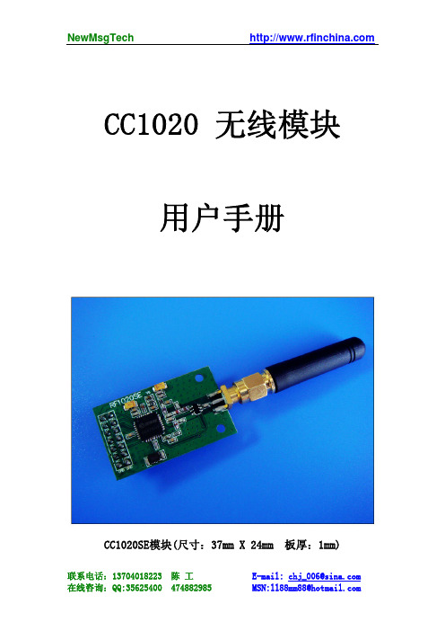
E-mail: chj_006@ MSN:ll88mm88@
NewMsgTech
产品概述
该模块使用 TI 公司的 CC1020 芯片开发而成。模块工作在 402,424, 426, 429, 433, 447,449, 469, 868 and 915 MHz 的 ISM和SRD频段,完全集成的位同步器。具有很低的IF特性,输出 的解调数据在DIO引脚产生,可以通过位同步时钟DCLK读取解调 数据及发送模式下的数据输出。数据包协议软件添加前导码、同 步字、地址信息和发送数据长度等。可以很容易通过SPI 接口进 行编程配置,电流消耗很低在发射功率为+10dBm 时发射电流为 27.1mA,接收电流为19.9mA. CC1020通信属于低速窄带传输,具 有通信距离远优点。
模块工作流程 _______________________________________________________5 初始化流程 _______________________________________________________6 工作模式切换流程: _______________________________________________6 发送数据流程 __________________________________________________7 接收数据流程 __________________________________________________7 数据包协议 _______________________________________________________7
CM-WIFI模块用户手册

CM-WIFI模块用户手册深圳市顾美科技有限公司V6.1版目录1、硬件说明 (1)1-1.模块型号及外观.......................................................................................................................................................................................11-2.指示灯.......................................................................................................................................................................................................11-3.参数及天线...............................................................................................................................................................................................21-4.主要应用领域...........................................................................................................................................................................................22、设置及使用指南.. (3)2-1.Web 管理页面介绍....................................................................................................................................................................................32-2.打开管理网页...........................................................................................................................................................................................32-3.快速联网设置...........................................................................................................................................................................................42-4.系统信息页面...........................................................................................................................................................................................52-5.STA 设置页面............................................................................................................................................................................................62-6.AP 设置页面..............................................................................................................................................................................................82-7.网络设置页面.........................................................................................................................................................................................102-8.串口设置页面.........................................................................................................................................................................................102-9.其他设置页面.........................................................................................................................................................................................112-10.账号管理页面.......................................................................................................................................................................................122-11.固件升级页面.......................................................................................................................................................................................132-12.重启页面...............................................................................................................................................................................................132-13.恢复页面...............................................................................................................................................................................................143、应用案例 (15)3-1.STA 接口连接调试.................................................................................................................................................................................153-2.AP 接口连接调试...................................................................................................................................................................................184、虚拟串口 (22)4-1.虚拟串口软件参数.................................................................................................................................................................................224-2.虚拟串口软件使用---STA 接口连接调试设置....................................................................................................................................22CM-WIFI 模块用户手册CM-WIFI 模块是深圳市顾美科技有限公司开发生产的一款体积小巧功能强大的一体化的802.11b/g/n WIFI 的低功耗解决方案。
CC1101+PA+LNA无线模块详细资料
DescriptionCC1101PATR4S is an FSK Transceiver module. The CC1101PATR4S is a true single-chip UHF transceiver, It base on 3 wire digital serial interface and an entire Phase-Locked Loop (PLL) for precise local oscillator generation .so the frequency could be setting. It can use in UART / NRZ / Manchester encoding / decoding. CC1101PATR4S had a high performance and low cost. It could easily to design your product.It can be used on wireless security system or specific remote-control function and others wireless systemFeaturesl Integrated bit synchronizer. l Integrated IF and data filters.l High sensitivity (type -115dBm at 2.4kbps) l Programmable output power -20dBm~30dBm l Operation temperature range : -40℃~+85℃ l Operation voltage: 5Volts.l Available frequency at : 408~464 MHz l Digital RSSIl Digital function for package formatApplicationsl Car security systeml Remote keyless entry ò Garage door controller ò Home security l Wireless mouse l Automation system433M 带PA远距离无线模块专业生产无线模块Pin DimensionPIN#Pin name Pin type Description 1 GND Ground GND2 PA_VCC PA power 3.3-9V PA power3 +3V3 power3.3V4 SI Digital input Serial configuration interface, data input 433M 带PA远距离无线模块6 SO Digital Output Serial configuration interface, clock inputOptional general output pin when CSN is hight7 GDO2 Digital Output Digital output pin for general use;8 GDO0 Digital I/O Digital output pin for general use;9 CSN Digital input Serial configuration interface ,chip select10 TX-EN TX_EN TX enable11 RX-EN RX-EN RX enableElectrical SpecificationsTc = 25°C, VDD = 5.0VParameter Min Typ Max Unit ConditionCurrent consumption, TX 300 350 380 mA Transmit mode, +30dBm output power 9VPA_VCCCurrent consumption, TX 100 150 180 mA Transmit mode, +20dBm output power 3.3VPA_VCCCurrent consumption, RX 15 20 30 receiverCurrent consumption,STB TAB Stand byGeneral CharacteristicsParameter Min Typ Max Unit Condition/NoteFrequencyrange408 433 464 MHzData rate 1.2 ……500 kbps Modulation formats supported: (Shaped) MSK (also known asdifferential offset QPSK) up to 500kbps2-FSK up to 500kbpsGFSK and OOK/ASK (up to 250kbps)Optional Manchester encoding (halves the data rate).CC1101 RF Receive SectionTc = 25°C, VDD = 3.0VParameter Min Typ Max Unit Condition/NoteDifferential inputmpedanceTBD ΩFollow CC1101EM reference designReceiver sensitivity 315/433/868/915MHz -110 –115 dBm 2-FSK, 1.2kbps, 5.2kHz deviation, 1% packet error rate, 62bytes packet length, 58kHz digital channel filter bandwidth-100 –105 dBm 2-FSK, 38.4kbps, 20kHz deviation, 1% packet error rate, 62bytes packet length, 100kHz digital channel filter bandwidth专业生产无线模块89 -92 dBm OOK, 250kbps OOK, 1% packet error rate, 62 bytes packetlength,540kHz digital channel filter bandwidthSaturation –15 dBmDigital channel filter bandwidth 58 650 kHz User programmable. The bandwidth limits are proportional tocrystal frequency (given values assume a 26.0MHz crystal).Adjacent channel rejection, 868MHz 23 dB 2-FSK, 38.4kbps, 20kHz deviation, 1% packet error rate, 62bytespacket length, 100kHz digital channel filter, 150kHz channelspacing Desired channel 3dB above the sensitivity limitAlternate channel rejection, 868MHz 33 dB 2-FSK, 38.4kbps, 20kHz deviation, 1% packet error rate, 62bytes packet length, 100kHz digital channel filter, 150kHzchannel spacing Desired channel 3dB above the sensitivitylimit.Image channel rejection, 868MHz 29 dB 2-FSK, 38.4kbps, 20kHz deviation, 1% packet error rate, 62bytes packet length, 100kHz digital channel filter, 150kHzchannel spacing, IF frequency 305kHz Desired channel 3dBabove the sensitivity limit.Blocking at 1MHz offset, 868MHz 52 dB Desired channel 3dB above the sensitivity limit. Compliant toETSIEN 300 220 class 2 receiver requirement.Blocking at 2MHz offset, 868MHz 54 dB Desired channel 3dB above the sensitivity limit. Compliant toETSIEN 300 220 class 2 receiver requirement.Blocking at 5MHz offset, 868MHz 61 dB Desired channel 3dB above the sensitivity limit. Compliant toETSI EN 300 220 class 2 receiver requirement.Blocking at 10MHz offset, 868MHz 64 dB Desired channel 3dB above the sensitivity limit. Compliant toETSI EN 300 220 class 2 receiver requirement.Spurious emissions –57–47 dBmdBm25MHz – 1GHz Above 1GHz专业生产无线模块CC1101 RF Transmit Section433M 带PA远距离无线模块Crystal Oscillator433M 带PA远距离无线模块CC1101 Simplified Block DiagramSchemactic N/ACC1101` Selectivity433M 带PA远距离无线模块专业生产无线模块Selectivity at 1.2K Baud Data RateSelectivity at 38.4K Baud Data RateSelectivity at 250K Baud Data RateMark:1. About Detail Specifications , Pls see CC1101 Data sheet ./lit/ds/symlink/CC1101.pdf 2SK30782SK3078 CharcteristicAS179 RF Switch。
CC1125高性能窄带无线模块
CC1125高性能窄带无线模块详细介绍:概述CC1125-TR-4S 基于 TI(德州仪器) Chipcon 的 CC1125无线收发芯片设计,是一款完整的、体积小巧的、低功耗的无线收发模块。
CC1125是 TI Chipcon 推出的 ISM 频段高性能无线收发芯片之一,主要设定为 170 / 315 / 433 / 868 / 915 / 920 / 950 MHz ISM/ SRD频段,最大输出功率可达 15dBm,最高传输速率达 200Kbps。
用户不需要对射频电路设计深入了解,就可以使用本模块轻易地开发出性能稳定、可靠性高的无线产品。
基本特点1、中心频率为433MHz,可工作于410-480MHz范围2、最大输出功率达15dBm,空旷地传输距离1200米以上3、高接收灵敏度,达-123dBm(1.2Kbps)4、支持2-FSK, 2-GFSK,4-FSK, 4-GFSK, MSK, OOK调制方式,可编程控制5、通信速率0~200Kbs,可编程配置6、独立的64byte发射/接收数据缓冲区7、内置CRC校验,确保数据可靠传输8、支持载波侦听功能9、数字RSSI输出10、低功耗,接收电流<26mA(high performance mode),发射电流<47mA (at +14 dBm)11、具有低功耗工作模式,功耗<0.3uA12、WOR功能可设置待机和接收状态切换时间以降低功耗13、集成温度传感器14、4线SPI接口,通用性强15、窄带通讯,邻道抑制可达-67dB,抗干扰强16、体积小:23.0×15.0×2.4 mm17、供电电压:2.0~3.6V DC应用范围1、物流跟踪、仓库巡检、电子标签等2、替代232、485进行无线数据通信3、工业仪器仪表无线数据采集和控制4、AMR(水、电、煤气)三表抄表5、建筑物与住宅(智能家居)控制6、电子消费类产品无线遥控7、无线报警与安全系统8、远距离无线传感器网络CC2500MTR2.4/CC2500邦定模块详细介绍:一、产品介绍CC2500MTR无线模块,工作于2.4GHz的 ISM/SRD频段免许可证使用,采用TI公司的CC2500多通道RF收发器,晶片邦定测试制造而成。
CC1100无线模块使用说明

CC1101无线模块使用说明书目录1.功能介绍 (2)2.引脚说明 (3)3.通信协议 (4)4.指令集 (5)4.1.芯片状态字节 (5)4.2配置寄存器 (6)5.操作函数 (8)5.1. 操作步骤 (8)5.2.函数 (9)1)读写一个字节 (9)2)写命令 (9)4)读取配置 (10)5)写入一串数据 (10)6)读取一串数据 (10)7)发送一组数据 (11)8)接收一组数据 (11)9)初始化配置 (12)10)设置接收模式 (13)11)设置发送模式 (13)1.功能介绍1.1.射.(RF.性能:1)采用 TI 最新的 CC110L 无线射频芯片, 软件完全兼容 CC1100, CC1101, 相比于前两者, CC110L 芯片更专注核心部分, 因此更稳定2)接收灵敏度低至−116 dBm(在 1 kbps 数据速率下,典型状态下-110dBm)3)可编程数据速率: 范围 0.6 至 600 kbps(推荐 2.4kbps--500kbps)4)工作于 433 MHz 免费 ISM 频段(387-464MHz, 推荐中心频点 430-436MHz)5)调制方式: 支持 2-FSK、4-FSK、GFSK 和 OOK(不支持 MSK 调制方式)1.2.数字特性:1)64 字节接收 (RX) 和发送 (TX) FIFO2)模块可软件设地址, 只有收到本机地址时才会输出数据(提供中断指示), 可直接接各种单片机使用, 软件编程非常方便1.3.低功耗特性:1)睡眠模式电流消耗约 2uA2)最大发射功率: +10dBm, 最大发射电流 30mA, 持续接收电流约 16mA3)快速启动时间: 240 uS(从睡眠模式到接收 [RX] 模式或发送[TX]模式)4)快速切换: 模块在接收 [RX]和发射[TX]模式切换时间 < 1ms1.4.接口及传输特性:1)采用标准 2.54mm 间距双排针接口方式。
沈阳风华双兴电子 FC211 SP 微功率无线数传模块 使用说明

沈阳风华双兴电子FC211/SP微功率无线数传模块使用说明沈阳风华双兴电子有限公司 SHENYANG FHSXTEC ELECTRONIC CO.,LTD.电话:(024)24152949 传真: (024)24152949 地址: 沈阳市东陵区万柳塘路56号3楼311室微功率无线数传模块使用说明书一、FC211SP微功率无线数传模块功能特点:1、频率在ISM频段(载波频率433MHz),无需申请频点。
2、抗干扰能力和低误码率。
基于FSK的调制方式,采用高效信道编码技术,提高了数据抗突发干扰和随机干扰的能力。
3、传输性能优良。
在视距情况下,天线位置高度>2米,可靠传输距离>800m(BER=10¯6/2400Bit/S)。
4、接口多样,设置使用方便。
提供三种接口方式:TTL/RS232/RS485提供透明的数据接口,接口波特率为1200/2400/4800/9600Bit/s,格式为8N1/8E1/8O1用户可设置。
空中波特率为1200/2400/4800/9600Bit/s用户可设置。
5、多信道。
模块标准配置提供8个信道,满足用户多种通信组合方式(根沈阳风华双兴电子 1微功率无线数传模块使用说明书据用户不同要求可扩展多信道)。
6、大的数据缓冲区。
在数据传输时1次至少转输750BYTES以上的数据帧,当空中波特率>串口波特率时,一次可传输200K字节以上的数据帧。
7、透明的数据传输、智能数据控制,它是一种半双工工作方式,对用户相当于一个半双工的串口设备。
通信时用户无需其它控制,只要从接口收/发数据即可,其它如空中收/发转换,控制等操作,模块能够自动完成。
8、低功耗TTL接口时,休眠电流<3uA,接收电流<28mA,发射电流≤70mA。
9、高可靠性,体积小,重量轻采用单片射频集成电路及单片MCU,外围电路少,可靠性高。
沈阳风华双兴电子 2微功率无线数传模块使用说明书二、FC211SP 微功率无线数传模块的使用方法1、接口位置示意图FC211SP 接口位置示意图 2、体积和重量体积:45mmX30mmX10mm重量:10克(不包括天线)沈阳风华双兴电子 3微功率无线数传模块使用说明书3、FC211SP接口的定义:J1 用户接口1)、IDLE:省电模式选择,悬空或低电平时有效,高(3.0V)电平处于活动模式。
CC1121 数据手册

High Performance Low Power RF TransceiverApplicationsUltra low power wireless systems with channel spacingdown to 50 kHz170 / 315 / 433 / 868 / 915 / 920 / 950 MHz ISM/SRDband systemsWireless Metering and Wireless Smart Grid (AMR andAMI)IEEE 802.15.4g systemsHome and building automationWireless alarm and security systemsIndustrial monitoring and controlWireless healthcare applicationsWireless sensor networks and Active RFIDRegulationsSuitable for systems targeting compliance with:Europe ETSI EN 300 220ETSI EN 54-25US FCC CFR47 Part 15FCC CFR47 Part 24Japan ARIB STD-T108Key FeaturesHigh performance single chip transceivero Excellent receiver sensitivity:-120 dBm at 1.2 kbps-110 dBm at 50 kbpso Blocking performance: 86 dB at 10 MHzo Adjacent channel selectivity: 60 dBo Very low phase noise: -111 dBc/Hz at 10 kHzoffsetPower Supplyo Wide supply voltage range (2.0 V – 3.6 V)o Low current consumption:- RX: 2 mA in RX Sniff Mode- RX: 17 mA peak current in low power mode- RX: 22 mA peak current in highperformance mode- TX: 45 mA at +14 dBmo Power down: 0.3 μAProgrammable output power up to +16 dBm with0.4 dB step sizeAutomatic output power rampingConfigurable data rates: 1.2 to 200 kbpsSupported modulation formats: 2-FSK, 2- GFSK,4-FSK, 4-GFSK, MSK, OOKWaveMatch: Advanced digital signal processing forimproved sync detect performanceRoHS compliant 5x5mm QFN 32 packagePeripherals and Support FunctionsEnhanced Wake-On-Radio functionality for automaticlow-power receive pollingSeparate 128-byte RX and TX FIFOsIncludes functions for antenna diversity supportSupport for re-transmissionsSupport for auto-acknowledge of received packetsTCXO support and control, also in power modesAutomatic Clear Channel Assessment (CCA) for listen-before-talk (LBT) systemsBuilt in coding gain support for increased range androbustnessDigital RSSI measurementSupport for seamless integration with the CC1190 forincreased range giving up to 3 dB improvement insensitivity and up to +27 dBm output powerTemperature sensorDescriptionThe CC1121is a fully integrated single-chip radiotransceiver designed for high performance at very lowpower and low voltage operation in cost effective wirelesssystems. All filters are integrated, removing the need forcostly external SAW and IF filters. The device is mainlyintended for the SRD (Short Range Device) frequencybands at 274-320 MHz, 410-480 MHz and 820-960 MHz.The CC1121 provides extensive hardware support for packethandling, data buffering, burst transmissions, clearchannel assessment, link quality indication and Wake-On-Radio. The CC1121 main operating parameters can becontrolled via an SPI interface. In a typical system, theCC1121 will be used together with a microcontroller and onlyfew external passive components.CSnSO (GPIO1)DVDD AVDD_IF RBIAS AVDD_RFGPIO0RESET_NGPIO3GPIO2DVDDVDD_GUARDCC1121LNA_PLNA_NDCPL_VCOAVDD_SYNTH1TRX_SWVDD_PFD_CHPXOSC_Q2XOSC_Q1CPL_PFD_CHPDCPLPASIN.C.DCPL_XOSCAVDD_XOSCSCLKEXT_XOSCLPF0LPF1AVDD_SYNTH2Table of Contents1ELECTRICAL SPECIFICATIONS (3)1.1A BSOLUTE M AX R ATINGS (3)1.2G ENERAL C HARACTERISTICS (3)1.3RF C HARACTERISTICS (3)1.4R EGULATORY S TANDARDS (4)1.5C URRENT C ONSUMPTION,S TATIC M ODES (5)1.6C URRENT C ONSUMPTION,T RANSMIT M ODES (5)1.7C URRENT C ONSUMPTION,R ECEIVE M ODES (6)1.8R ECEIVE P ARAMETERS (6)1.9T RANSMIT P ARAMETERS (11)1.10PLL P ARAMETERS (12)1.11W AKE-UP AND T IMING (13)1.1232MH Z C RYSTAL O SCILLATOR (13)1.1332MH Z C LOCK I NPUT (TCXO) (13)1.1432 K H Z C LOCK I NPUT (14)1.1532 K H Z RC O SCILLATOR (14)1.16I/O AND R ESET (14)1.17T EMPERATURE S ENSOR (14)2TYPICAL PERFORMANCE CURVES (15)3PIN CONFIGURATION (17)4BLOCK DIAGRAM (18)4.1F REQUENCY S YNTHESIZER (18)4.2R ECEIVER (18)4.3T RANSMITTER (19)4.4R ADIO C ONTROL AND U SER I NTERFACE (19)4.5E NHANCED W AKE-O N-R ADIO (E WOR) (19)4.6S NIFF M ODE (19)4.7A NTENNA D IVERSITY (20)4.8L OW P OWER /H IGH P ERFORMANCE M ODE (20)5TYPICAL APPLICATION CIRCUIT (21)6HISTORY (22)PRODUCTION DATA information is current as of publication date. Products conform to1Electrical SpecificationsAll measurements performed on CC1120EM_868_915 rev.1.0.1, CC1120EM_955 rev.1.2.1, CC1120EM_420_470 rev.1.0.1 or CC1120EM_169 rev.1.21.1Absolute Max Ratings1.2General CharacteristicsPRODUCTION DATA information is current as of publication date. Products conform to1.4Regulatory StandardsPRODUCTION DATA information is current as of publication date. Products conform toPRODUCTION DATA information is current as of publication date. Products conform toT A = 25°C, VDD = 3.0 V if nothing else stated1.6 Current Consumption, Transmit Modes950 MHz band (High Performance Mode)T A = 25°C, VDD = 3.0 V if nothing else stated868/915/920 MHz bands (High Performance Mode)T A = 25°C, VDD = 3.0 V if nothing else stated434 MHz band (High Performance Mode)T A = 25°C, VDD = 3.0 V if nothing else stated170 MHz band (High Performance Mode)T A = 25°C, VDD = 3.0 V if nothing else statedLow Power ModeT A = 25°C, VDD = 3.0 V, f c = 869.5 MHz if nothing else statedPRODUCTION DATA information is current as of publication date. Products conform toHigh Performance ModeT A = 25°C, VDD = 3.0 V, f c = 869.5 MHz if nothing else statedLow Power ModeT A = 25°C, VDD = 3.0 V, f c = 869.5 MHz if nothing else stated 1.8Receive Parameters 1General Receive Parameters (High Performance Mode)T A = 25°C, VDD = 3.0 V, f c = 869.5 MHz if nothing else stated1All RX measurements made at the antenna connector, to a bit error rate limit of 1%RX performance in 950 MHz band (High Performance Mode)T A = 25°C, VDD = 3.0 V if nothing else stated2 DEV is short for deviation, CHF is short for Channel Filter Bandwidth3 BT=0.5 is used in all GFSK measurementsPRODUCTION DATA information is current as of publication date. Products conform toRX performance in 868/915/920 MHz bands (High Performance Mode) T A = 25°C, VDD = 3.0 V if nothing else statedPRODUCTION DATA information is current as of publication date. Products conform toPRODUCTION DATA information is current as of publication date. Products conform toRX performance in 434 MHz band (High Performance Mode)T A = 25°C, VDD = 3.0 V if nothing else statedRX performance in 170 MHz band (High Performance Mode)T A = 25°C, VDD = 3.0 V if nothing else statedRX performance in Low Power ModeT A = 25°C, VDD = 3.0 V, f c = 869.5 MHz if nothing else statedPRODUCTION DATA information is current as of publication date. Products conform to1.9Transmit ParametersT A = 25°C, VDD = 3.0 V, f c = 869.5 MHz if nothing else statedPRODUCTION DATA information is current as of publication date. Products conform to1.10PLL ParametersHigh Performance ModeT A = 25°C, VDD = 3.0 V, f c = 869.5 MHz if nothing else statedLow Power ModeT A = 25°C, VDD = 3.0 V, f c = 869.5 MHz if nothing else statedPRODUCTION DATA information is current as of publication date. Products conform toPRODUCTION DATA information is current as of publication date. Products conform to1.11 Wake-up and TimingT A = 25°C, VDD = 3.0 V, f c = 869.5 MHz if nothing else stated1.12 32 MHz Crystal OscillatorT A= 25°C, VDD = 3.0 V if nothing else stated1.13 32 MHz Clock Input (TCXO)T A = 25°C, VDD = 3.0 V if nothing else stated1.1432 kHz Clock InputT A = 25°C, VDD = 3.0 V if nothing else stated1.1532 kHz RC OscillatorT A = 25°C, VDD = 3.0 V if nothing else stated.1.16I/O and ResetT A = 25°C, VDD = 3.0 V if nothing else stated1.17Temperature SensorT A = 25°C, VDD = 3.0 V if nothing else statedThe CC1121 can be configured to provide a voltage proportional to temperature on GPIO1. Using the information above, the temperature can be estimated by measuring this voltage. Please refer to the CC1121 user guide for more information.PRODUCTION DATA information is current as of publication date. Products conform toPRODUCTION DATA information is current as of publication date. Products conform to2 Typical Performance CurvesT A = 25°C, VDD = 3.0 V, f c = 869.5 MHz if nothing else statedAll measurements performed on CC1120EM_868_915 rev.1.0.1, CC1120EM_955 rev.1.2.1, CC1120EM_420_470 rev.1.0.1 or CC1120EM_169 rev.1.2Note that the "output power vs load impedance" plot was measured at the 50 Ω antenna connectorOutput Power at 868MHz vs PA power setting-50-40-30-20-10010207F7B77736F6B67635F5B57534F4B4743PA power settingO u t p u t P o w e r (d B m)TX Current at 868MHz vs PA power setting 01020304050607F7B77736F6B67635F5B57534F4B4743PA power settingT X C u r r e n t (m A )Output Power vs Voltage Max Setting, 170 MHz68101214161822.533.5Supply Voltage (V)O u t p u t P o w e r (d B m )Output Power vs Temperature Max Setting, 170 MHz, 3.6V1515.51616.517-404080Temperature (ºC)O u t p u t P o w e r (d B m )PRODUCTION DATA information is current as of publication date. Products conform toGPIO Output Low Voltage vs Current Being Sinked020040060080010001200140005101520253035Current (mA)G P I O O u t p u t L o w V o l t a g e (m V)GPIO Output High Voltage vs Current Being Sourced1.51.71.92.12.32.52.72.93.105101520253035Current (mA)G P I O O u t p u t h i g h V o l t a g e (V)3Pin ConfigurationThe CC1121 pin-out is shown in the table below.PRODUCTION DATA information is current as of publication date. Products conform to4Block DiagramA system block diagram of CC1121 is shown Figure 4.1.(optional 32kHzclock intput)(optional autodetectedexternal XOSC / TCXO)Figure 4.1 : System Block Diagram4.1Frequency SynthesizerAt the heart of CC1121there is a fully integrated, fractional-N, ultra high performance frequency synthesizer. The frequency synthesizer is designed for excellent phase noise performance, providing very high selectivity and blocking performance. The system is designed to comply with the most stringent regulatory spectral masks at maximum transmit power.Either a crystal can be connected to XOSC_Q1 and XOSC_Q2, or a TCXO can be connected to the EXT_XOSC input. The oscillator generates the reference frequency for the synthesizer, as well as clocks for the ADC and the digital part. To reduce system cost, CC1121 has high accuracy frequency estimation and compensation registers to measure and compensate for crystal inaccuracies, enabling the use of lower cost crystals. If a TCXO is used, the CC1121will automatically turn the TCXO on and off when needed to support low power modes and Wake-On-Radio operation.4.2ReceiverCC1121features a highly flexible receiver. The received RF signal is amplified by the low-noise amplifier (LNA) and down-converted in quadrature (I and Q) to the intermediate frequency (IF). At IF, the I/Q signals are digitized by the high dynamic range ADCs.An advanced Automatic Gain Control (AGC) unit adjusts the front end gain, and enables the CC1121 to receive both strong and weak signals, even in the presence of strong interferers. High attenuation channel and data filtering enable reception with strong neighbor channel interferers. The I/Q signal is converted to a phase / magnitude signal to support both FSK and OOK modulation schemes.PRODUCTION DATA information is current as of publication date. Products conform toA sophisticated pattern recognition algorithm locks onto the synchronization word without need for preamble settling bytes. Receiver settling time is therefore reduced to the settling time of the AGC, typically 4 bits. The advanced pattern recognition also greatly reduces the problem of false sync triggering on noise, further reducing power consumption and improving sensitivity and reliability. The pattern recognition logic can also be used as a high performance preamble detector to reliably detect a valid preamble in the channel.A novel I/Q compensation algorithm removes any problem of I/Q mismatch and hence avoids time consuming and costly I/Q / image calibration steps in production or in the field.4.3TransmitterThe CC1121 transmitter is based on direct synthesis of the RF frequency (in-loop modulation). To achieve effective spectrum usage, CC1121 has extensive data filtering and shaping in TX to support high throughput data communication in narrowband channels. The modulator also controls power ramping to remove issues such as spectral splattering when driving external high power RF amplifiers.4.4Radio Control and User InterfaceThe CC1121 digital control system is built around MARC (Main Radio Control) implemented using an internal high performance 16 bit ultra low power processor. MARC handles power modes, radio sequencing and protocol timing.A 4-wire SPI serial interface is used for configuration and data buffer access. The digital baseband includes support for channel configuration, packet handling, and data buffering. The host MCU can stay in power down until a valid RF packet has been received, and then burst read the data, greatly reducing the power consumption and computing power required from the host MCU.The CC1121radio control and user interface is based on the widely used CC1101transceiver to enable easy SW transition between the two platforms. The command strobes and the main radio states are the same for the two platforms.For legacy formats CC1121 also has support for two serial modes. In synchronous serial mode CC1121 performs bit synchronization and provides the MCU with a bit clock with associated data. In transparent mode CC1121 outputs the digital baseband signal using a digital interpolation filter to eliminate jitter introduced by digital filtering and demodulation.4.5Enhanced Wake-On-Radio (eWOR)eWOR, using a flexible integrated sleep timer, enables automatic receiver polling with no intervention from the MCU. The CC1121 will enter RX, listen and return to sleep if a valid RF packet is not received. The sleep interval and duty cycle can be configured to make a trade-off between network latency and power consumption. Incoming messages are time-stamped to simplify timer re-synchronization.The eWOR timer runs off an ultra low power 32 kHz RC oscillator. To improve timing accuracy, the RC oscillator can be automatically calibrated to the RF crystal in configurable intervals.4.6Sniff ModeThe CC1121 supports very quick start up times, and requires very few preamble bits. Sniff Mode uses this to dramatically reduce the current consumption while the receiver is waiting for data. Since the CC1121 is able to wake up and settle much faster than the length of most preambles, it is not required to be in RX continuously while waiting for a packet to arrive. Instead, the enhanced wake-on-radio feature can be used to put the device into sleep periodically. By setting an appropriate sleep time, the CC1121 will be able to wake up and receive the packet when it arrives with no performance loss. This removes the need for accurate timing synchronization betweenPRODUCTION DATA information is current as of publication date. Products conform totransmitter and receiver, and allows the user to trade off current consumption between the transmitter and receiver.4.7Antenna DiversityAntenna diversity can increase performance in a multi-path environment. An external antenna switch is required. The switch can be automatically controlled by CC1121using one of the GPIO pins (also support for differential output control signal typically used in RF switches).If antenna diversity is enabled, the GPIO will alternate between states until a valid RF input signal is detected. An optional acknowledge packet can be transmitted without changing GPIO state.An incoming RF signal can be validated by received signal strength, by using the automatic preamble detector, or a combination of the two. Using the preamble detector will make a more robust system and avoid the need to set a defined signal strength threshold, as this threshold will set the sensitivity limit of the system.4.8Low Power / High Performance ModeThe CC1121 is highly configurable, enabling trade-offs between power and performance to be made based on the needs of the application. This data sheet describes two modes - low power mode and high performance mode - which represent configurations where the device is optimized for either power or performance.PRODUCTION DATA information is current as of publication date. Products conform to5Typical Application CircuitVery few external components are required for the operation of CC1121. A typical application circuit is shown below. Note that it does not show how the board layout should be done, which will greatly influence the RF performance of CC1121.This section is meant as an introduction only. Note that decoupling capacitors for power pins are not shown in the figure below.OptionalCC1121SPI interface andoptional gpio pinsFigure 5.1 : Typical Application CircuitPRODUCTION DATA information is current as of publication date. Products conform to6HistoryPRODUCTION DATA information is current as of publication date. Products conform toPACKAGING INFORMATION(1) The marketing status values are defined as follows:ACTIVE: Product device recommended for new designs.LIFEBUY: TI has announced that the device will be discontinued, and a lifetime-buy period is in effect.NRND: Not recommended for new designs. Device is in production to support existing customers, but TI does not recommend using this part in a new design.PREVIEW: Device has been announced but is not in production. Samples may or may not be available.OBSOLETE: TI has discontinued the production of the device.(2) Eco Plan - The planned eco-friendly classification: Pb-Free (RoHS), Pb-Free (RoHS Exempt), or Green (RoHS & no Sb/Br) - please check /productcontent for the latest availability information and additional product content details.TBD: The Pb-Free/Green conversion plan has not been defined.Pb-Free (RoHS): TI's terms "Lead-Free" or "Pb-Free" mean semiconductor products that are compatible with the current RoHS requirements for all 6 substances, including the requirement that lead not exceed 0.1% by weight in homogeneous materials. Where designed to be soldered at high temperatures, TI Pb-Free products are suitable for use in specified lead-free processes.Pb-Free (RoHS Exempt): This component has a RoHS exemption for either 1) lead-based flip-chip solder bumps used between the die and package, or 2) lead-based die adhesive used between the die and leadframe. The component is otherwise considered Pb-Free (RoHS compatible) as defined above.Green (RoHS & no Sb/Br): TI defines "Green" to mean Pb-Free (RoHS compatible), and free of Bromine (Br) and Antimony (Sb) based flame retardants (Br or Sb do not exceed 0.1% by weight in homogeneous material)(3) MSL, Peak Temp. -- The Moisture Sensitivity Level rating according to the JEDEC industry standard classifications, and peak solder temperature.(4) There may be additional marking, which relates to the logo, the lot trace code information, or the environmental category on the device.(5) Multiple Device Markings will be inside parentheses. Only one Device Marking contained in parentheses and separated by a "~" will appear on a device. If a line is indented then it is a continuation of the previous line and the two combined represent the entire Device Marking for that device.Important Information and Disclaimer:The information provided on this page represents TI's knowledge and belief as of the date that it is provided. TI bases its knowledge and belief on information provided by third parties, and makes no representation or warranty as to the accuracy of such information. Efforts are underway to better integrate information from third parties. TI has taken andAddendum-Page 1continues to take reasonable steps to provide representative and accurate information but may not have conducted destructive testing or chemical analysis on incoming materials and chemicals. TI and TI suppliers consider certain information to be proprietary, and thus CAS numbers and other limited information may not be available for release.In no event shall TI's liability arising out of such information exceed the total purchase price of the TI part(s) at issue in this document sold by TI to Customer on an annual basis.Addendum-Page 2TAPE AND REEL INFORMATION*All dimensions are nominal Device Package Type Package DrawingPinsSPQ Reel Diameter (mm)Reel Width W1(mm)A0(mm)B0(mm)K0(mm)P1(mm)W (mm)Pin1Quadrant CC1121RHBR VQFNRHB 323000330.012.4 5.3 5.3 1.58.012.0Q2CC1121RHBT VQFNRHB 32250180.012.4 5.3 5.3 1.58.012.0Q2CC1121RHMR VQFN RHM 323000330.012.4 5.3 5.3 1.58.012.0Q2Pack Materials-Page 1*All dimensions are nominalDevice Package Type Package Drawing Pins SPQ Length(mm)Width(mm)Height(mm) CC1121RHBR VQFN RHB323000338.1338.120.6 CC1121RHBT VQFN RHB32250210.0185.035.0 CC1121RHMR VQFN RHM323000338.1338.120.6Pack Materials-Page2IMPORTANT NOTICETexas Instruments Incorporated and its subsidiaries(TI)reserve the right to make corrections,enhancements,improvements and other changes to its semiconductor products and services per JESD46,latest issue,and to discontinue any product or service per JESD48,latest issue.Buyers should obtain the latest relevant information before placing orders and should verify that such information is current and complete.All semiconductor products(also referred to herein as“components”)are sold subject to TI’s terms and conditions of sale supplied at the time of order acknowledgment.TI warrants performance of its components to the specifications applicable at the time of sale,in accordance with the warranty in TI’s terms and conditions of sale of semiconductor products.Testing and other quality control techniques are used to the extent TI deems necessary to support this warranty.Except where mandated by applicable law,testing of all parameters of each component is not necessarily performed.TI assumes no liability for applications assistance or the design of Buyers’products.Buyers are responsible for their products and applications using TI components.To minimize the risks associated with Buyers’products and applications,Buyers should provide adequate design and operating safeguards.TI does not warrant or represent that any license,either express or implied,is granted under any patent right,copyright,mask work right,or other intellectual property right relating to any combination,machine,or process in which TI components or services are rmation published by TI regarding third-party products or services does not constitute a license to use such products or services or a warranty or endorsement e of such information may require a license from a third party under the patents or other intellectual property of the third party,or a license from TI under the patents or other intellectual property of TI.Reproduction of significant portions of TI information in TI data books or data sheets is permissible only if reproduction is without alteration and is accompanied by all associated warranties,conditions,limitations,and notices.TI is not responsible or liable for such altered rmation of third parties may be subject to additional restrictions.Resale of TI components or services with statements different from or beyond the parameters stated by TI for that component or service voids all express and any implied warranties for the associated TI component or service and is an unfair and deceptive business practice. TI is not responsible or liable for any such statements.Buyer acknowledges and agrees that it is solely responsible for compliance with all legal,regulatory and safety-related requirements concerning its products,and any use of TI components in its applications,notwithstanding any applications-related information or support that may be provided by TI.Buyer represents and agrees that it has all the necessary expertise to create and implement safeguards which anticipate dangerous consequences of failures,monitor failures and their consequences,lessen the likelihood of failures that might cause harm and take appropriate remedial actions.Buyer will fully indemnify TI and its representatives against any damages arising out of the use of any TI components in safety-critical applications.In some cases,TI components may be promoted specifically to facilitate safety-related applications.With such components,TI’s goal is to help enable customers to design and create their own end-product solutions that meet applicable functional safety standards and requirements.Nonetheless,such components are subject to these terms.No TI components are authorized for use in FDA Class III(or similar life-critical medical equipment)unless authorized officers of the parties have executed a special agreement specifically governing such use.Only those TI components which TI has specifically designated as military grade or“enhanced plastic”are designed and intended for use in military/aerospace applications or environments.Buyer acknowledges and agrees that any military or aerospace use of TI components which have not been so designated is solely at the Buyer's risk,and that Buyer is solely responsible for compliance with all legal and regulatory requirements in connection with such use.TI has specifically designated certain components as meeting ISO/TS16949requirements,mainly for automotive use.In any case of use of non-designated products,TI will not be responsible for any failure to meet ISO/TS16949.Products ApplicationsAudio /audio Automotive and Transportation /automotiveAmplifiers Communications and Telecom /communicationsData Converters Computers and Peripherals /computersDLP®Products Consumer Electronics /consumer-appsDSP Energy and Lighting /energyClocks and Timers /clocks Industrial /industrialInterface Medical /medicalLogic Security /securityPower Mgmt Space,Avionics and Defense /space-avionics-defense Microcontrollers Video and Imaging /videoRFID OMAP Applications Processors /omap TI E2E Community Wireless Connectivity /wirelessconnectivityMailing Address:Texas Instruments,Post Office Box655303,Dallas,Texas75265Copyright©2013,Texas Instruments Incorporated。
CC1101收发一体无线模块

最小值 典型值 最大值
-20
25
75
1.8
3.6
928
单位 ℃ VDC MHz
备注
3.3 直流特性(除非另有说明,否则温度=25℃,Vcc=3.3V)
描述 VDD电源 RX模式电流 睡眠模式电流 数据速率
最小值 典型值 最大值
1.8
3.6
16
30
小于
2
1.2
500K
单位 VDC mA uA bps
备注
.2.
W-RT-C01S8
1.4 组件选配
■ 测试架一对(含6按键发射底板一个、带LED指示同时蜂鸣器发声的接收底板一个); ■ 标准SMA-315MHz、433MHz天线(胶棒天线、弹簧天线、单芯铜导线、0.8mm漆包线); ■ 标准AA电池(9V方形电池,主板LDO设计可DC-DC降为3.3V、5V电源); ■ 客户待评估模块(收发模块2个,模块样品请联系销售申请); ■ SMA双头高频线1根(客户研发部门需配置高频信号源、频谱仪、数字示波器等);
单位
MHz dbm dbm kb/s
.6.
W-RT-C01S8
4.引脚信号和接口定义
4.1 引脚功能描述
W-RX-P01D6模块具有单路串行数据口,用于连接到用户的MCU上。模块各引脚的功能如 下表所示:
表4-1 I/O 引脚分配
Pin1 … …… …Pin8
NO. 引脚# 引脚名称
1 PIN-1 VDD
2.1 PCB布局要求
◆要有好的RF性能,适当的PCB布局是非常重要的。在可容许范围内,建议使用双层PCB 布局以便于在其中一层可以加上连续的接地平面。大量的via holes可以将上层接地部分 连接至下层的接地平面。 ◆在CC1101内部,电源与接地线是分开的,各有独立的区块各自提供偏压使得最小的噪声效应。 ◆电压振幅变化较大的控制线和数字信号线路必须远离LAN与OSC共振器件以避免造成干扰。
捷麦 CW10 型 WiFi 模块用户手册说明书
--V1.1CW10型网口模块 DESCRIPITION OF PRODUCTS北京捷麦通信器材有限公司 *************版权声明北京捷麦通信器材有限公司版权所有,并保留对本手册及本声明的最终解释权和修改权。
本手册的版权归北京捷麦通信器材有限公司所有。
未得到北京捷麦通信器材有限公司的书面许可,任何人不得以任何方式或形式对本手册内的任何部分进行复制、摘录、备份、修改、传播、翻译成其它语言、将其全部或部分用于商业用途。
免责声明本手册依据现有信息制作,其内容如有更改,恕不另行通知。
北京捷麦通信器材有限公司在编写该手册的时候已尽最大努力保证其内容准确可靠,但不对本手册中的遗漏、不准确或印刷错误导致的损失和损害承担责任。
我们会经常对手册中的数据进行检查,并在后续的版本中进行必要的更正。
欢迎您提出宝贵意见。
技术支持北京捷麦通信器材有限公司建立了以总部技术支持中心、区域技术支持中心和本地技术支持中心为主体的完善的服务体系,并提供电话热线服务。
您在产品使用过程中遇到问题时可随时与北京捷麦通信器材有限公司技术支持服务热线联系。
此外,您还可以通过北京捷麦通信器材有限公司网站及时了解最新产品动态,以及下载需要的技术文档。
北京捷麦通信器材有限公司:地址:北京市丰台区芳城园一区日月天地B座1505邮编:100017电话:************/6/7传真:************E-mail:****************网站:阅读指南手册目标通过阅读该用户手册,可以了解CW10的外观结构及安装、知道CW10如何与PC计算机连接通信、熟悉CW10的各种工作模式及其参数意义,会使用参数配置软件完成对CW10的参数操作,依据常用功能的调试流程应用CW10产品的基本功能。
使得用户完全能够应用本产品所提供的所有功能。
阅读对象本手册为具有一定工控背景知识的工程人员、安装人员及电气人员编写,其内容涵盖了CW10的安装、功能模式讲解和调试等信息。
CC1110 无线部分中文参考手册
CC1110无线部分中文参考手册版本:V1.002009年3月23日·andyla·ZigBee&IAR学习小组无线CC1110Fx/CC1111Fx的简化结构图如上Figure47.低中频(10w-IF)接收是CC1110的特性之一。
CC1110'收到的RF信号被低噪声放大器(LNA)放大,并且将收到的同相信号和正交相位信号(1/Q)降频转换为中频(IF)信号。
过滤掉残余在中频(2MHz)信号中的1/Q信号后,放大中频信号。
在中频信号中通过ADC数字化、自动增益控制,以及精细信道的过滤、解调字节和包同步(byte synchronization)等,所有这些都通过数字逻辑完成。
CC1110的发射端基于RF频率直接合成。
频率合成器包括一套完整的片上电感器电容器(LC)、电压控制振荡器(VCO)和一个90度移相器,用来产生同相信号、正交相位信号(I/Q)和本地振荡器(LO)信号给接收端的降频合成器。
26M的晶振作为频率合成器产生参考频率,同时为ADC和数字部分提供时钟脉冲。
一个特殊寄存器作为CPU访问的数据缓冲区。
配置和状态寄存器统一映射到外部XDATA区的寄存器进行访问。
数字基频包括频带配置支持,数据包处理和数据缓冲。
一个片上电压管理器用来调节传递1.8V的供电电压.15.1CPU使用了一系列选通命令来控制CC1110的无线操作。
选通命令可以看成是单字节指令,每条命令用来控制某个无线模块的功能。
这些命令可以实现使能频率合成器、使能接收模式、使能发送模式,以及其他功能。
图33简化状态表及典型用法和电流消耗上图33中展示了一个简化状态表及典型用法和电流消耗。
该表表明了在选通控制命令下的状态转换。
想看完整的状态转换机图可参考15.12节图中命令简介:FSTXON:快速TX准备TX_OFF_MODE:发送完数据时下一步选择做什么RX_OFF_MODE:接收到数据后下一步选择做什么选通命令通过写RFST寄存器发出。
VT-CC1101PA-433无线模块规格书

版权 @ 2010, 深圳市芯威科技有限公司
VTRF1101PA- MARCH-2010-REVISED
电话: +86-755-88844812 传真: +86-755-22643680 网址: 地址:中国广东省深圳市南山区科技园麒麟路 1 号科技创业服务中心大厦 612-613
产品特征
输出功率大于20dBm,传输距离可达800m以上 433MHz无线收发器,可订制315M/868M/915M等其它载频 支持 FSK, GFSK, ASK/OOK 以及MSK调制方式 可编程配置传输数率1.2k - 500 kbps 内置前向纠错 FEC,灵敏度高 点对点,点对多点,灵活通信方式 RSSI输出和载波侦听指示 SMD元件23.0*15.0*2.4 mm,体积小 使用廉价的微控制器可得高性能RF系统 SPI接口
技术参数
VT-CC1101PA-433 无线模块
技术指标 工作电压 工作频率 频率误差 调制方式 输出功率 接收灵敏度 接收电流 发射电流 待机电流 传输速率 数据接口 通讯距离 天线阻抗 存贮温度 工作温度 外形尺寸
参数 直流2.4-3.6V 433MHz +-10KHz FSK/GFSK/ASK/OOK/MSK >20dBm -110dB 20mA 90mA 2uA 1.2-500Kbps SPI 接口 800m 50ohm -50 - 150°C -40 - 85 °C 23.0*15.0*2.4 mm
描述 直流2.4-3.6V输入
数据输入 时钟输入 数据输出 数据输出,由寄存器配置 数据输出,由寄存器配置 模块选择 阻抗50ohm 发射为低电平,接收为高电平 发射为高电平,接收为低电平
短距离无线数据收发系统课程设计说明书
课程设计短距离无线数据收发系统设计概括射频技术作为本世纪最有前途的信息技术之一,一直受到业界的高度重视。
该技术采用射频进行非接触式双向通信,可自动识别目标物体并获取相关数据。
这是一个基于CC1101通信模块的简单无线通信系统。
该系统由发射模块和接收模块组成。
它以STC89C51单片机为核心,以单片机应用技术和无线收发技术为理论基础,实现数据和状态的无线收发。
节目。
系统传输距离可达2km。
该研究成果对无线通信的普及具有重要意义。
关键词:STC89C52; CC1100H模块;无线收发器;简介41设计任务分析41.1无线收发器原理概述41.2课题研究背景及意义41.3设计内容及要求42硬件电路设计52. 1 STC89C51 单片机52.2CC1100H通信模块61.2.1 CC1100H 模块介绍62. 2.2 CC1100H模块底座设计72.3电源电路设计72.3.1供电方式72.3. 2电源部分对射频电路的抗干扰设计73.3. 3模组电源解决方案83.4串口83.5MCU 与CC1100H 模块的SPI 接口9 3无线通信模块的编程与实现93.1CC1100H 模块93.2CC1100H 模块SPI 接口介绍103.3CC1100H模块无线收发流程113.4CC1100H模块收发程序设计93.5. 1通信模块致数据的部分程序及注释10 10接收数据的部分程序及注释10介绍近年来,在信息通信领域,无线通信技术是发展最快、应用最广泛的技术。
无线通信技术具有集成化、低功耗、易操作的发展趋势。
目前,一些仅由微控制器和集成射频。
PC-RS-1212 UTC 系列无线透传模块 说明书

PC-RS-1212用户手册UTC系列无线透传模块PC-1212功能特点概述 (2)第一:如何安装PC-1212驱动 (2)第二:如何使用跳线来设置SETA和SETB的电平 (3)第三:如何通过PC-1212进行无线通信功能测试 (3)第四:如何进行PC-1212模块自身参数配置 (5)RS-1212功能特点概述 (6)第一:RS-1212模块接口定义 (6)第二:RS-1212模块注意事项 (7)PC-1212功能特点概述PC-1212模块是一款USB接口的串口无线数传模块,专门为上位机设备无线数传应用而设计,一般与UTC1212数传模块相配套使用,主要应用于下位机(MCU)与上位机(PC电脑端)数据的无线接收和发送。
以下介绍一下PC-1212模块的功能特点和使用方法。
第一: 如何安装PC-1212驱动(1) 双击驱动程序即可安装,默认提供XP、WIN7系统驱动,其他系统驱动,请网上搜索下载:PL2303HX驱动(如PL2303HX VISTA驱动)(2) 将PC-1212插入PC的USB接口,通过硬件设备管理器查看,当电脑设备管理器出现如下图所示,既表示安装成功。
使用时以此根据选择虚拟COM 端口。
第二:如何使用跳线来设置SETA和SETB的电平如下图所示,打开PC-1212模块外壳可以看到模块有2个零欧姆电阻,当该零欧姆电阻在0标识一侧表示SET-A(或者SET-B)电平为低电平(接地), 当该零欧姆电阻焊接在1标识一侧表示SET-A(或者SET-B)电平为高电平(3.3V),PC-1212出厂默认都为0,即正常通信模式。
通过零欧姆的位置来设置SETA和SETB电平,可以组合出多种工作模式,对应工作模式的特性详细请查看与UTC1212无线透传模块相对应的开发手册。
第三:如何通过PC-1212进行无线通信功能测试当我们通过前几步骤,我们已经熟悉了PC-1212模块的基本特性,然后我们可以通过最常用的串口助手软件来进行无线收发数据测试了。
cc2500大功率无线模块规格书说明

1:产品介绍
CC2500PATR2.4S 是 集 FSK/ASK/OOK/MSK. 调 制方式于一体的收发模块。 它提供扩展硬件支持实现信息包处 理、数据缓冲、群发射、空闲信道评估、链接 质量指示和无 线电波唤醒,可以采用曼彻斯特编码进行调制解调它的数据 流。 性能优越并且易于应用到你的产品设计中,它可以应用 于 2400-2483.5MHz ISM/SRD 频段的系统,消费类电子产 品、无线游戏控制器、无线音频传输和 其他的无线系统中。
CC2500PA1无线模块
使用说明
第 1 页
产品目录
1: 产品介绍……………………………………………………………………...4 2:产品特征…………………………………………………………………….4 3:应用范围…………………………………………………………………….4 4:性能参数…………………………………………………………………….5 5:外形尺寸…………………………………………………………………….6 6:引脚定义…………………………………………………………………….7 7:应用电路简介……………………………………………………………….7
?testsignals?测试信号?fifostatussignals?先进先出堆栈状态信号?clearchannelindicator?空闲信道指示?clockoutputdowndividedfromxosc?时钟输出从xosc分频?serialoutputrxdata?serialconfigurationinterfacechipselect串行输出接收数据8csndigitalinput串行配置接口芯片选择9paendigitalinputwhentxstatusset1rxset0tx发射状态时设置为1rx接收设置为0whenrxstatusset1txset0rx接收状态时设置为1tx发射设置10lnaendigitalinput为07
深圳市泰达鑫通信技术 TDX-1150 无线数传模块 说明书
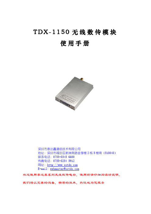
T D X-1150无线数传模块使用手册深圳市泰达鑫通信技术有限公司地址:深圳市福田区新洲南路金享楼2栋5楼南(518048)联系电话:0755-8345 6600传真电话:0755-8254 5912网址:E-mail: webmaster@欢迎使用泰达鑫系列无线数传电台,使用前请仔细阅读该说明。
我们将以完善的设备,精湛的技术,热忱地为您服务一.TDX-1150无线数传模块特点1.功率发射500mW。
2.无线数据传输433MHz免向无委申请频段(430MHz~470MHz)。
3.高抗干扰能力和低误码率。
基于GFSK的调制方式,提高了数据抗随机干扰和突发干扰的能力,在信道误码率为10-2时,可得到实际误码率10-5~10-6。
4.传输距离远。
在开阔视距情况下,天线放置高度位置>2米,9600bps可靠传输距离大于1500m (BER=10-3/9600bps);1200bps传输距离可达2500m (BER=10-3/1200bps)。
5.透明的数据传输。
提供透明的数据接口,能适应任何标准或非标准的用户协议。
自动过滤掉空中产生的假数据(所收即所发)。
6.可编程信道。
TDX-1150在同一个频段可以按照用户自行通过设置软件修改信道频点(能被25KHz整除的频点),满足用户选择不同使用频点。
7.提供3种接口方式。
TDX-1150提供3选1接口方式,TTL电平UART接口或标准电平的RS-232或标准的RS-485口。
8.可提供自组网方式。
TDX-1150无线模块常规提供透明传输方式;可根据用户需求定做自组网方式的软件,模块的硬件部分不变。
9.大的数据缓冲区。
接口波特率等于空中有效波特率:1200/2400/4800/9600bps(接口速率19200bps可定做);数据格式为8N1/8E1/8O1用户自定义,可传输无限长的数据帧,用户编程更灵活。
11.智能数据控制,用户无需编制多余的程序。
即使是半双工通信,用户也无需编制多余的程序,只要从接口收/发数据即可,其它如空中收/发转换,控制等操作,TDX-1150模块自动完成。
- 1、下载文档前请自行甄别文档内容的完整性,平台不提供额外的编辑、内容补充、找答案等附加服务。
- 2、"仅部分预览"的文档,不可在线预览部分如存在完整性等问题,可反馈申请退款(可完整预览的文档不适用该条件!)。
- 3、如文档侵犯您的权益,请联系客服反馈,我们会尽快为您处理(人工客服工作时间:9:00-18:30)。
CC1121-433M无线模块
规格书
概述
CC1121-433M基于TI Chipcon的CC1121无线收发芯片设计,是一款完整的、体积小巧的、低功耗的无线收发模块。
CC1121是TI Chipcon推出的ISM频段无线收发芯片之一,主要设定为170/433/868/915/950MHz频段,最大输出功率可达+15dBm,最高传输速率达200Kbps。
模块集成了所有射频相关功能,用户不需要对射频电路设计深入了解,就可以使用本模块轻易地开发出性能稳定、可靠性高的无线产品。
基本特点
●433MHz无线收发器,可定制170M/868M/915M/950M等其它载频
●支持2-FSK, 2-GFSK, 4-FSK,4-GFSK,MSK,OOK/ASK调制
●-11 – 15dBm功率输出可配制
●在1.2kbps速率时接收灵敏度可达-123dBm ●可编程配置传输数率1.2 - 200 kbps
●低功耗2.0~3.6V 供电
●点对点,点对多点,灵活通信方式
●RSSI输出和载波侦听指示
●独立128字节RX和TX FIFO
●高稳定性,可靠性达到工业级别
●SMD元件
应用范围
●无线计量和无线智能电网
●物流跟踪、仓库巡检、电子标签等
●工业仪器仪表无线数据采集和控制
●住宅与建筑物(智能家居)控制
●电子消费类产品无线遥控
●无线报警与安全系统
●无线传感器网络
25.8*20.9*1.8 (mm)
技术参数
测试条件:Ta=25°C,VCC=3.3V
备注:
1.模块的通信速率会影响通信距离和接收灵敏度,速率越高,通信距离越近。
2.模块的供电电压会影响发射功率,在工作电压范围内,电压越低,发射功率越小。
3.模块的工作温度变化时,中心频率会改变,只要不超出工作温度范围,不影响应用。
4.天线对通信距离有很大的影响,请选用匹配的天线并正确安装。
5.模块的安装方式会影响通信距离。
接口说明
引脚定义
接口电路
注:以上模块引脚排列并非按实际排列,引脚排列请看引脚定义。
SPI、数据输出接口请与MCU实际功能引脚连接。
电路中请做好ESD保护,防止因引脚输入造成电路损坏。
为保证射频性能,请注意模块布局、地线分布、天线安装。
有不明之处可与我司技术人员联系。
程序设计
CC1121寄存器配置值可用SmartRF Studio工具产生,各寄存器的意义请参阅CC1121芯片规格书。
同时,我们可提供配套的评估套件和相关例程,方便用户开发和评估模块的性能。
我们的评估套与TI SmartRF04套件的功能相同,可直接连接SmartRF Studio以控制CC1121,也可以用我们自己例程演示CC1121模块的通信效果。
外形尺寸
配套天线
我们可以提供与模块匹配的天线,如用户对天线有特殊要求,我们可以配合用户选择天线,帮助用户调试天线的匹配问题。
注意:标配天线是免费的,可选天线需要用户购买,价格根据天线的规格而定。
常见故障及排除方法
开发资料:
1121芯片规格书(CC1121.pdf)
1121寄存器配置工具(SmartRF Studio 7 v1.4.9.zip)
1121例程(CC1121 Demo Code.rar)
4.开发板(TI Chipcon Evaluation Board)。