HCNR200电压隔离
模拟光耦HCNR200、HCNR201应用笔记

HCNR200和HCNR201模拟光电耦合器SPICE电路仿真应用笔记AN5545Jamshed Namdar Khan,安华高科技(Avago Technologies)隔离应用产品事业部光电耦合器应用工程师介绍本应用笔记的目的是展示PSpice软件如何通过使用安华高科技(Avago Technologies)提供的PSpice宏模型精确预测和仿真Avago公司HCNR200和HCNR201模拟光电耦合器的行为,聚焦集成电路仿真程序(SPICE, Sim-ulation Program with Integrated Circuit Emphasis)目前被认为是模拟电路设计工程师不可或缺的工具。
相对模拟光电耦合器数据表参数或规格,良好的宏模型应该精确预测电路性能,PSpice或SPICE仿真是任何设计工程师成功完成设计项目一个必备并且不可或缺的工具,电路仿真有助于原始设计概念的发想,从而允许工程师调整并优化原型电路取得最佳可能电路性能。
电路仿真的最大优势在于建构实体硬件或进行性能测试前可以先行验证并改善设计,极小化花费在原型测试的时间和相关费用成本。
为何需要仿真?不管电路仿真可以如何进行或带来什么,有一点它绝不可能做到的是为你提供实际的电路设计,因此我们首先列举几个吸引设计工程师进行电路仿真的原因。
进行电路仿真的主要动力是极小化预测目标电路设计性能的时间,相较于实际建立和进行原型测试等效电路的评估,使用SPICE电路进行评估所使用的时间相对上非常微小,另外,这些电路仿真也可以在各种不同温度、偏置条件以及零组件数值和误差条件下多次进行,但耗费时间仅为进行电路试验板设计并于工作台上进行评估的数分之一。
在进行光电耦合器SPICE仿真时,首先应该了解的是软件并无法仿真光电耦合器的两个基本特性,设计工程师使用光电耦合器主要有两个理由,分别是绝缘和隔离,SPICE软件并无法对这两个主要关键光电耦合器功能建立模型。
线性光耦隔离检测电压电路

线性光耦隔离检测电压电路耦合器以光为媒介传输电信号。
它对输入、输出电信号有良好的隔离作用,所以,它在各种电路中得到广泛的应用。
目前它已成为种类最多、用途最广的光电器件之一。
光耦合器一般由三部分组成:光的发射、光的接收及信号放大。
输入的电信号驱动发光二极管(LED),使之发出一定波长的光,被光探测器接收而产生光电流,再经过进一步放大后输出。
这就完成了电—光—电的转换,从而起到输入、输出、隔离的作用。
由于光耦合器输入输出间互相隔离,电信号传输具有单向性等特点,因而具有良好的电绝缘能力和抗干扰能力。
又由于光耦合器的输入端属于电流型工作的低阻元件,因而具有很强的共模抑制能力。
所以,它在长线传输信息中作为终端隔离元件可以大大提高信噪比。
在计算机数字通信及实时控制中作为信号隔离的接口器件,可以大大增加计算机工作的可靠性。
线性光耦的电流传输特性曲线接近直线,并且小信号时性能较好,能以线性特性进行隔离控制。
线性光耦TIL300 :主要技术指标如下:1.带宽>200Kz;2.传输增益稳定度为±0.05%/℃3.峰值隔离电压为3500VTIL300是一个由红外光LED照射分叉配置的隔离反馈光二极管和一个输出光二极管组成。
该器件采用特殊制造技术来补偿LED时间和温度特性的非线性,使输出信号与发出的伺服光通量成线性比例。
图1.TIL300电容C 防止电路产生震荡。
TIL300内部D0是发光二极管,其工作电流电If 可选为10mA 。
D1,D2为光敏二极管,他们受D0的激发分别产生电流Ip1和Ip2,其大小与If 有关:其中 、 表明 , 随 的变化,可称为光耦合函数。
由于D1,D2用相同的工艺做成并与D0封装在一起,因此,它们的光耦合函数变化规律一致,故可设:(1)实际上可以把K 看做常数,K 的值是TIL300的电器参数,典型值为1。
参数取值范围为0.75~1.25.。
U1构成一个负反馈放大器,其同相输入端和反相输入端的电压应近似相等,满足:(2) U2是一个电压跟随器,输出电压V0等于输入段电压:22i p V I R » (3) 于是电路的增益可由 (4)由于i V 的电压是由R3、R4、R5分压后输入U1同向端,所以: 0222111P i P V I R R K V I R R ==2p I 1p I f I 2f K I 11p fI K I = 1f K I 22p fI K I = 2211p f p f I K I K I K I == 11i p V I R »(5)于是: (6)可以看出输出0V 与E 是线性关系。
光耦的作用
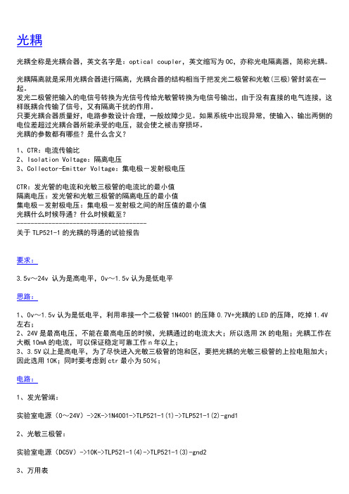
光耦光耦全称是光耦合器,英文名字是:optical coupler,英文缩写为OC,亦称光电隔离器,简称光耦。
光耦隔离就是采用光耦合器进行隔离,光耦合器的结构相当于把发光二极管和光敏(三极)管封装在一起。
发光二极管把输入的电信号转换为光信号传给光敏管转换为电信号输出,由于没有直接的电气连接,这样既耦合传输了信号,又有隔离干扰的作用。
只要光耦合器质量好,电路参数设计合理,一般故障少见。
如果系统中出现异常,使输入、输出两侧的电位差超过光耦合器所能承受的电压,就会使之被击穿损坏。
光耦的参数都有哪些?是什么含义?1、CTR:电流传输比2、Isolation Voltage:隔离电压3、Collector-Emitter Voltage:集电极-发射极电压CTR:发光管的电流和光敏三极管的电流比的最小值隔离电压:发光管和光敏三极管的隔离电压的最小值集电极-发射极电压:集电极-发射极之间的耐压值的最小值光耦什么时候导通?什么时候截至?-------------------------------------关于TLP521-1的光耦的导通的试验报告要求:3.5v~24v 认为是高电平,0v~1.5v认为是低电平思路:1、0v~1.5v认为是低电平,利用串接一个二极管1N4001的压降0.7V+光耦的LED的压降,吃掉1.4V 左右;2、24V是最高电压,不能在最高电压的时候,光耦通过的电流太大;所以选用2K的电阻;光耦工作在大概10mA的电流,可以保证稳定可靠工作n年以上;3、3.5V以上是高电平,为了尽快进入光敏三极管的饱和区,要把光耦的光敏三极管的上拉电阻加大;因此选用10K;同时要考虑到ctr最小为50%;电路:1、发光管端:实验室电源(0~24V)->2K->1N4001->TLP521-1(1)->TLP521-1(2)-gnd12、光敏三极管:实验室电源(DC5V)->10K->TLP521-1(4)->TLP521-1(3)-gnd23、万用表直流电压挡20V万用表+-> TLP521-1(4)万用表--> TLP521-1(3)试验结果输入电源万用表电压(V)1.3V 51.5V 4.81.7V 4.411.9V 3.582.1V 2.942.3V 1.82.5V 0.582.7V 0.22.9V 0.193.1V 0.173.3V 0.163.5V 0.165V0.1324V0.06-----------------------------------------光耦是用来隔离输入输出的,主要是隔离输入的信号。
HCNR200201
1前言通常隔离放大器都具有极好的抗共模干扰能力,还可有效阻断现场和数据采集系统之间的电联系,但并不切断它们之间的信号传递,在通信、工业、医疗器材、电源及测试装置等系统之中,电路的隔离是必要的,传统的实现的隔离都是由变压器及光耦合元件完成的,其中变压器用于耦合交流信号;而光耦合器则用于直流信号的耦合。
与一般的光耦合元件不同,LOC11X 光耦合器可工作在伺服模式,并能用以补偿发光二极管的非线性时间及温度特性,除此之外,LOC11X 光耦合器还能同时耦合交流及直流信号,为设计者提供了可取代大体积变压器及非线性光耦合元件的更佳选择。
2结构原理LOC11X光耦合器有LOC110、LOC111和LOC112三种型号,其内部结构为一个红外线发光二极管与两个光电三极管形成的光耦合。
其中的一个光电三极管可在伺服反馈机制中对发光二极管的导通电流予以补偿;另一个光电三极管用于提供输入及输出电路间的电流隔离。
图1所示是LOC11X的内部结构及引脚排列。
LOC11X光耦合器有DIP和表面贴装两种封装形式,它们均能耦合模拟和数字信号,且具有高增益稳定性,其带宽大于200kHz,线性度可达0.01%。
由于LOC11X光耦合器内部有一对线性光耦合器,应当用在电流隔离,可保持正确的交流及直流信号的耦合以及输入/输出的线性,它有光电压和光电导两种工作模式。
2.1光电导模式图2是LOC11X光耦合器在光电导模式下工作的典型电路,该电路被配置成光电三极管的集电极与基极反向偏压,这是LOC11X光耦合器在光电导模式下运作的典型接法。
当输入电压VIN在0V且IF为0mA时,U1有一个大的开环增益值,而随着VIN值的升高,U1的输出值开始进入VCC1的轨迹上,随着U1输出的增大,IF 开始有电流值,发光二极管也进入工作状态。
接着,光电三极管受到发光二极管所发出光的照射而导通并产生电流I1,当I1流经R1时,将在U1的反相端产生电压VA,从而使得放大器进入负反馈工作状态。
针对HCNR200线性光耦隔离电路的带宽的脉冲测试法[发明专利]
![针对HCNR200线性光耦隔离电路的带宽的脉冲测试法[发明专利]](https://img.taocdn.com/s3/m/14fe69f0d4bbfd0a79563c1ec5da50e2524dd13d.png)
(19)中华人民共和国国家知识产权局(12)发明专利申请(10)申请公布号 (43)申请公布日 (21)申请号 201811273474.8(22)申请日 2018.10.30(71)申请人 北京航空航天大学地址 100191 北京市海淀区学院路37号(72)发明人 高成 寇震梦 黄姣英 王乐群 (74)专利代理机构 北京慧泉知识产权代理有限公司 11232代理人 王顺荣 唐爱华(51)Int.Cl.G01R 31/28(2006.01)G01R 31/00(2006.01)(54)发明名称针对HCNR200线性光耦隔离电路的带宽的脉冲测试法(57)摘要本发明提供一种针对HCNR200线性光耦隔离电路的带宽的脉冲测试法,其步骤如下:一:选择HCNR200线性光耦隔离电路并进行配置;二:搭建测试隔离电路带宽所用的测试系统;三:对HCNR200线性光耦隔离电路开展带宽测试;四:对HCNR200线性光耦隔离电路带宽测试数据进行处理和分析;通过以上步骤,针对HCNR200线性光耦隔离电路的带宽进行测试,利用被测隔离电路对脉冲信号的响应上升沿时间与被测电路的带宽之间的关系,发挥脉冲信号频率特性的优势,达到测试HCNR200线性光耦隔离电路的带宽的目的。
反映HCNR200线性光耦器件在实际应用中隔离传输高频信号的能力。
权利要求书2页 说明书4页 附图3页CN 109471013 A 2019.03.15C N 109471013A1.一种针对HCNR200线性光耦隔离电路的带宽的脉冲测试方法,其特征在于:其步骤如下:步骤一:选择HCNR200线性光耦隔离电路并进行配置;先查找HCNR200线性光耦数据手册中的隔离电路,选择高速低成本模拟型隔离电路;然后对选择的隔离电路进行配置;绘制电路结构图并制作高速低成本模拟型隔离电路的印制电路板即PCB电路板;将电阻、三极管和HCNR200线性光耦焊接到PCB电路板上;该HCNR200线性光耦为双列直插式封装即DIP8,管脚1连接三极管Q2N3904的集电极;管脚2连接5V DC电压源;管脚3连接R1电阻;管脚4、5连接地线;管脚6连接三极管Q2N3906的基极;管脚7、8空置;步骤二:搭建测试隔离电路带宽所用的测试系统;该测试系统由脉冲信号源、HCNR200线性光耦隔离电路、示波器、5V电压源和计算机组成;其中待测隔离电路的输入端与脉冲信号源的信号输出端连接,脉冲信号源的输出端连接示波器的一通道探头,待测隔离电路的输出端连接示波器的二通道探头,通用接口总线即GPIB连接脉冲源与计算机,GPIB线连接示波器与计算机;使用5V电压源对隔离电路供电使其能够正常工作;步骤三:对HCNR200线性光耦隔离电路开展带宽测试;首先调节脉冲信号源参数,然后将脉冲源调整至信号输出状态,使脉冲信号通过待测隔离电路,使用示波器采集到隔离电路的输入信号和隔离电路的响应信号波形;步骤四:对HCNR200线性光耦隔离电路带宽测试数据进行处理和分析;针对步骤三中示波器采集到的隔离电路的响应曲线,选取响应信号幅值上升至10%时所对应的时间记为t1,幅值上升至90%时所对应的时间记为t2;被测HCNR200线性光耦隔离电路对脉冲信号的响应上升沿时间为τr=t2-t1式中:τr为被测HCNR200线性光耦隔离电路对脉冲信号的响应上升沿时间;当脉冲信号通过HCNR200线性光耦隔离电路时,由于高频分量的丢失产生波形变化并体现在响应曲线上升沿时间上,经过时域和频域的转换分析,响应上升沿时间与电路的带宽具有如下的关系:式中:B是HCNR200线性光耦器件的隔离电路带宽;由此得HCNR200线性光耦隔离电路的带宽;通过以上步骤,利用HCNR200线性光耦隔离电路对脉冲信号的响应信号上升沿时间与电路的带宽之间的关系,发挥脉冲信号频率特性的优势,达到了测试HCNR200线性光耦隔离电路的带宽的目的;对于测试HCNR200线性光耦在实际应用时能够隔离传输的信号的频率范围具有重要的参考意义;本发明相对于扫频测试而言,不需要外加高频信号源来产生高频正弦波信号,而是采用脉冲信号源进行测试,能节约测试成本;取代多次扫频得出HCNR200线性光耦隔离电路的带宽的复杂步骤,经过一次脉冲信号的输入和一次响应信号的分析就能得到HCNR200线性光耦隔离电路的带宽,更加简单便捷。
使用线性光耦HCNR200制作交流电压测量模块

使用线性光耦HCNR200制作交流电压测量模块测量范围:幅值30V测量精度:0.5%误差电路自行设计,要求写好设计报告,制作出实物模块。
参考原理见/hiwxzh/blog/item/e145eff1965a43bba40f52a7.html1. 线性光耦介绍光隔离是一种很常用的信号隔离形式。
常用光耦器件及其外围电路组成。
由于光耦电路简单,在数字隔离电路或数据传输电路中常常用到,如UART协议的20mA电流环。
对于模拟信号,光耦因为输入输出的线形较差,并且随温度变化较大,限制了其在模拟信号隔离的应用。
对于高频交流模拟信号,变压器隔离是最常见的选择,但对于支流信号却不适用。
一些厂家提供隔离放大器作为模拟信号隔离的解决方案,如ADI的AD202,能够提供从直流到几K的频率内提供0.025%的线性度,但这种隔离器件内部先进行电压-频率转换,对产生的交流信号进行变压器隔离,然后进行频率-电压转换得到隔离效果。
集成的隔离放大器内部电路复杂,体积大,成本高,不适合大规模应用。
模拟信号隔离的一个比较好的选择是使用线形光耦。
线性光耦的隔离原理与普通光耦没有差别,只是将普通光耦的单发单收模式稍加改变,增加一个用于反馈的光接受电路用于反馈。
这样,虽然两个光接受电路都是非线性的,但两个光接受电路的非线性特性都是一样的,这样,就可以通过反馈通路的非线性来抵消直通通路的非线性,从而达到实现线性隔离的目的。
市场上的线性光耦有几中可选择的芯片,如Agilent公司的HCNR200/201,TI 子公司TOAS的TIL300,CLARE的LOC111等。
这里以HCNR200/201为例介绍2. 芯片介绍与原理说明HCNR200/201的内部框图如下所示其中1、2引作为隔离信号的输入,3、4引脚用于反馈,5、6引脚用于输出。
1、2引脚之间的电流记作IF,3、4引脚之间和5、6引脚之间的电流分别记作IPD1和IPD2。
输入信号经过电压-电流转化,电压的变化体现在电流IF上,IPD1和IPD2基本与IF成线性关系,线性系数分别记为K1和K2,即K1与K2一般很小(HCNR200是0.50%),并且随温度变化较大(HCNR200的变化范围在0.25%到0.75%之间),但芯片的设计使得K1和K2相等。
模拟光耦HCNR200、HCNR201应用笔记
HCNR200和HCNR201模拟光电耦合器SPICE电路仿真应用笔记AN5545Jamshed Namdar Khan,安华高科技(Avago Technologies)隔离应用产品事业部光电耦合器应用工程师介绍本应用笔记的目的是展示PSpice软件如何通过使用安华高科技(Avago Technologies)提供的PSpice宏模型精确预测和仿真Avago公司HCNR200和HCNR201模拟光电耦合器的行为,聚焦集成电路仿真程序(SPICE, Sim-ulation Program with Integrated Circuit Emphasis)目前被认为是模拟电路设计工程师不可或缺的工具。
相对模拟光电耦合器数据表参数或规格,良好的宏模型应该精确预测电路性能,PSpice或SPICE仿真是任何设计工程师成功完成设计项目一个必备并且不可或缺的工具,电路仿真有助于原始设计概念的发想,从而允许工程师调整并优化原型电路取得最佳可能电路性能。
电路仿真的最大优势在于建构实体硬件或进行性能测试前可以先行验证并改善设计,极小化花费在原型测试的时间和相关费用成本。
为何需要仿真?不管电路仿真可以如何进行或带来什么,有一点它绝不可能做到的是为你提供实际的电路设计,因此我们首先列举几个吸引设计工程师进行电路仿真的原因。
进行电路仿真的主要动力是极小化预测目标电路设计性能的时间,相较于实际建立和进行原型测试等效电路的评估,使用SPICE电路进行评估所使用的时间相对上非常微小,另外,这些电路仿真也可以在各种不同温度、偏置条件以及零组件数值和误差条件下多次进行,但耗费时间仅为进行电路试验板设计并于工作台上进行评估的数分之一。
在进行光电耦合器SPICE仿真时,首先应该了解的是软件并无法仿真光电耦合器的两个基本特性,设计工程师使用光电耦合器主要有两个理由,分别是绝缘和隔离,SPICE软件并无法对这两个主要关键光电耦合器功能建立模型。
复合励磁永磁同步发电机端电压采样隔离电路_线性光耦HCNR200的应用

收稿日期:20052102151 邓醉杰 男 1980年生;湖南大学电气与信息工程学院在读硕士研究生,研究方向为电力电子与电力传动.复合励磁永磁同步发电机端电压采样隔离电路———线性光耦HC NR200的应用邓醉杰 叶丽花 黄守道 周健湖南大学电气与信息工程学院,湖南长沙(410082)摘 要 本文设计了复合励磁永磁同步发电机端电压采样隔离电路,简要介绍了新型线性光耦器件HC NR200的工作原理,也给出了隔离电路的硬件电路图、参数计算公式及其注意事项。
通过实验证明该电路正确实用。
关键词 复合励磁 隔离电路 线性光耦HC NR200中图分类号T M313 文献标识码B 文章编号1008-7281(2006)02-0036-03Term i n a l Volt age Sam pli n g and Isol a ti n g C i rcu it of Co m pound Exc it a ti onPermanen tM agnet Synchronous Genera tor 2The Appli ca ti onof L i n ear O pti ca l Coupler HCNR 200D eng Zu ijie,Ye L ihua,Huang S houdao,and Zhou J ianAbstract The ter m inal voltage sa mp ling and is olating circuit of co mpound excitati onper manent magnet synchr onous generat or is designed in this paper,the p rinci p le of the ne w linear op tical coup ler HCNR200is si m p ly discussed,and the sche me of hardware of is olating circuit,para meter calculati on f or mulas and attenti ons are given .It is p r oved that the sche me is true and p ractical p r oved by experi m ents .Key words Compound excitati on,is olating circuit,op tical coup ler HCNR200.0 引言近年来,由于永磁电机技术、电力电子技术的迅速发展,多电源输出、高效、高可靠性和稳定性的新型移动电站成为了研究主导。
隔离型电流检测电路

线性光耦hcnr200中文资料

1. 线形光耦介绍光隔离是一种很常用的信号隔离形式。
常用光耦器件及其外围电路组成。
由于光耦电路简单,在数字隔离电路或数据传输电路中常常用到,如UART协议的20mA 电流环。
对于模拟信号,光耦因为输入输出的线形较差,并且随温度变化较大,限制了其在模拟信号隔离的应用。
对于高频交流模拟信号,变压器隔离是最常见的选择,但对于支流信号却不适用。
一些厂家提供隔离放大器作为模拟信号隔离的解决方案,如ADI的AD202,能够提供从直流到几K的频率内提供0.025%的线性度,但这种隔离器件内部先进行电压-频率转换,对产生的交流信号进行变压器隔离,然后进行频率-电压转换得到隔离效果。
集成的隔离放大器内部电路复杂,体积大,成本高,不适合大规模应用。
模拟信号隔离的一个比较好的选择是使用线形光耦。
线性光耦的隔离原理与普通光耦没有差别,只是将普通光耦的单发单收模式稍加改变,增加一个用于反馈的光接受电路用于反馈。
这样,虽然两个光接受电路都是非线性的,但两个光接受电路的非线性特性都是一样的,这样,就可以通过反馈通路的非线性来抵消直通通路的非线性,从而达到实现线性隔离的目的。
市场上的线性光耦有几中可选择的芯片,如Agilent公司的HCNR200/201,TI子公司TOAS的TIL300,CLARE的LOC111等。
这里以HCNR200/201为例介绍2. 芯片介绍与原理说明HCNR200/201的内部框图如下所示其中1、2引作为隔离信号的输入,3、4引脚用于反馈,5、6引脚用于输出。
1、2引脚之间的电流记作IF,3、4引脚之间和5、6引脚之间的电流分别记作IPD1和IPD2。
输入信号经过电压-电流转化,电压的变化体现在电流IF上,IPD1和IPD2基本与IF成线性关系,线性系数分别记为K1和K2,即K1与K2一般很小(HCNR200是0.50%),并且随温度变化较大(HCNR200的变化范围在0.25%到0.75%之间),但芯片的设计使得K1和K2相等。
基于线性光耦HCNR200的电流检测电路设计与实现

基于线性光耦HCNR200的电流检测电路设计与实现浙江大学生仪学院生物医学工程 **** 学号******[摘要]本文主要介绍了惠普公司的高线性度模拟光耦HCNR200的基本结构及工作原理。
利用该器件设计了一种模拟信号隔离来对医疗设备中电流检测的硬件电路,较好地解决了设备中高电压、强电流很容易串入低压器件会将其烧毁的问题。
线性光耦HCNR200可以较好地实现模拟量与数字量之间的隔离,隔离电压峰值达8000V;输出跟随输入变化,线性度达0.01%。
在高稳定性、高线性度的模拟信号隔离的场合具有广泛的应用前景。
[关键词]线性光耦HCNR200 模拟隔离电流检测1 引言在自动化检测系统、计算机数据采集系统、医疗设备控制系统等诸多工业测量中,光隔离是一种很常用的信号隔离形式。
常用光耦器件及其外围电路组成。
由于光耦电路简单,在数字隔离电路或数据传输电路中常常用到,如UART协议的20mA电流环。
对于模拟信号,光耦因为输入输出的线形较差,并且随温度变化较大,限制了其在模拟信号隔离的应用。
在信号采集的过程中,各种干扰信号都会随着被测量信号进入数字控制系统,这些信号迭加在有用的被测信号上会使测量的准确度降低,造成控制系统的不稳定。
为了实现电平线性转换以及不把现场的电噪声干扰引入到数字控制系统中来,必须将被测电路和控制电路在电气上实现隔离,光电隔离法和隔离放大器法是两种常用的模拟信号隔离方法。
隔离放大器内部集成有高性能的输入输出放大器、调制解调器、信号耦合变压器等单元器件,通常采用磁耦合方法使放大器的输出和输入之间没有电气联系,从而隔离了干扰源,抑制了干扰信号,完成对信号的放大。
隔离放大器具有完全浮动的输入端和独立隔离的输出端,并有良好的线性度和稳定性,还有较高的隔离电压和共模抑制比。
但是隔离放大器对于支流信号却不适用,价格比较高,只适用于要求较高的场合。
光电隔离是常用且方便有效的隔离方法,它是通过光电之间的相互转换,并利用光作为媒介进行信号传输,在电气上使测量系统与现场信号完全隔离。
HCNR200 SPICE电路仿真
HCNR200和HCNR201模拟光电耦合器SPICE电路仿真应用笔记AN5545Jamshed Namdar Khan,安华高科技(Avago Technologies)隔离应用产品事业部光电耦合器应用工程师介绍本应用笔记的目的是展示PSpice软件如何通过使用安华高科技(Avago Technologies)提供的PSpice宏模型精确预测和仿真Avago公司HCNR200和HCNR201模拟光电耦合器的行为,聚焦集成电路仿真程序(SPICE, Sim-ulation Program with Integrated Circuit Emphasis)目前被认为是模拟电路设计工程师不可或缺的工具。
相对模拟光电耦合器数据表参数或规格,良好的宏模型应该精确预测电路性能,PSpice或SPICE仿真是任何设计工程师成功完成设计项目一个必备并且不可或缺的工具,电路仿真有助于原始设计概念的发想,从而允许工程师调整并优化原型电路取得最佳可能电路性能。
电路仿真的最大优势在于建构实体硬件或进行性能测试前可以先行验证并改善设计,极小化花费在原型测试的时间和相关费用成本。
为何需要仿真?不管电路仿真可以如何进行或带来什么,有一点它绝不可能做到的是为你提供实际的电路设计,因此我们首先列举几个吸引设计工程师进行电路仿真的原因。
进行电路仿真的主要动力是极小化预测目标电路设计性能的时间,相较于实际建立和进行原型测试等效电路的评估,使用SPICE电路进行评估所使用的时间相对上非常微小,另外,这些电路仿真也可以在各种不同温度、偏置条件以及零组件数值和误差条件下多次进行,但耗费时间仅为进行电路试验板设计并于工作台上进行评估的数分之一。
在进行光电耦合器SPICE仿真时,首先应该了解的是软件并无法仿真光电耦合器的两个基本特性,设计工程师使用光电耦合器主要有两个理由,分别是绝缘和隔离,SPICE软件并无法对这两个主要关键光电耦合器功能建立模型。
线性光偶HCNR200的原理与电路设计
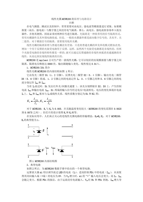
线性光偶HCNR200的原理与电路设计孙鹏在电气测量、测试以及控制中,常常需要对高电压、强电流等模拟量进行采集。
如果模拟量(高压、强电流)与数字量之间没有电气隔离,那么,高电压、强电流很容易串入低压器件,并将其烧毁,因而必须对两种信号进行隔离。
光隔离是一种很常用的信号隔离形式,常用光耦器件及其外围电路组成。
但是,一般的光偶器件都是面向数字信号的,具有开、关二值性,对于模拟信号的隔离,需要使用线形光耦。
线性光耦的隔离原理与普通光耦没有差别,只是将普通光耦的单发单收模式稍加改变,增加一个用于反馈的光接受电路用于反馈。
这样,虽然两个光接受电路都是非线性的,但两个光接受电路的非线性特性都是一样的,就可以通过反馈通路的非线性来抵消直通通路的非线性,从而达到实现线性隔离的目的。
HCNR200是Agilent 公司生产的一款线性光耦,它可以较好的实现模拟量与数字量之间隔离,隔离电压峰值达8000伏,输出跟随输入变化,线性度达0.01%。
1、HCNR200/201简介线性光耦HCNR200的内部结构如图 1所示。
它由发光二极管D1(1、2引脚)、反馈光电二极管D2(3、4引脚)、输出光电二极管D3(5、6引脚)组成。
1、2引脚之间的电流记作I F ,3、4引脚之间和5、6引脚之间的电流分别记作I PD1和I PD2。
当有I F 流过时,D1发出红外光(伺服光通量 )。
该光分别照射在D2、D3上,产生控制电流I PD1和输出电流I PD2。
D1两端的输入信号经过电压-电流转化,电压的变化体现在电流I F 上,I PD1和I PD2基本与I F 成线性关系,线性系数分别记为K1和K2,即:FPD F PD I I K I I K 2211,== 对于HCNR200,K 1与K 2为0.005,并且随温度变化较大(HCNR200的变化范围在0.0025到0.0075之间),但芯片的设计使得K 1和K 2相等。
在实际应用中,人们真正关心的是线性光偶电路的传输增益:K 3=K 2/K 1,对于HCNR200,K 3的典型值为1。
HCNR200电压隔离
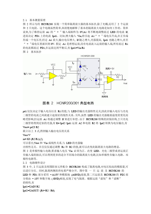
2. 1基本测量原理图2所示为用HCNR200实现一个简单隔离放大器的基本拓扑,除了光耦,还用了2个运放和2只电阻。
这个电路虽然简单,却清楚地解释了基本的隔离放大电路是如何工作的。
简单说来,为了维持运放A1的“+ ”输入端始终为0V,A1将不断地调整流过LED的电流If,进而决定PD1上的电流Ipd1。
比如,增大输入Vin,将引起A1“+ ”端电压升高,在正负端形成一个电压差,经过A1放大,输出电压增大, If随之增大,光强提高, Ipd1也随之增大,直至“+ ”端电压重新回到0V。
假定A1是理想运放,没有电流流入运放的输入端,所有流过R1的电流都流过PD1,在运放达到平衡后,有Ipd1=Vin/R1图2基本拓扑pd1仅仅决定于输入电压以及R1的值,与LED的输出光强特性无关,因此在输入电压与光电二极管的电流之间就建立起很好的线性关系。
另外,虽然LED的输出光强随着温度的变化而略受影响,但运放A1将通过调整If来进行补偿。
由于HCNR200特殊的封装结构, 2只光电二极管将得到近似的光强,有K= Ipd2/ Ipd1运放A2和电阻R2将Ipd2转换为电压输出,有Vout= pd23 R2联立以上3式,得到输入输出电压的关系V out/Vin= K3 (R2/R1)(2)可以看出,Vout和Vin成线性关系,与LED的光强输出特性无关。
并且仅仅通过调整R1和R2的值,就可以改变此隔离放大电路的增益。
图2是单极性输入电路,要求输入电压Vin必须为正。
改变LED、光电二极管或者运放正负输入端的接法,可以得到更多的适合不同场合的隔离放大电路,比如单极性负输入电路、双极性电路等。
2. 2电路硬件设计图3中, 2只运放及周围阻容元件配合HCNR200构成了隔离电路,对电压较高的模拟量,可以进行分压。
同时,隔离两侧的供电要严格分开。
图中第一只运放及HCNR200 的LED和PD1部分采用+ A18V和模拟地(AGND)连接,第二只运放及HCNR200的PD2部分则由+ 18V和数字地( GND)相连,实现了电气隔离。
线性光耦hcnr 中文

1. 线形光耦介绍光隔离是一种很常用的信号隔离形式。
常用光耦器件及其外围电路组成。
由于光耦电路简单,在数字隔离电路或数据传输电路中常常用到,如UART协议的20mA 电流环。
对于模拟信号,光耦因为输入输出的线形较差,并且随温度变化较大,限制了其在模拟信号隔离的应用。
对于高频交流模拟信号,变压器隔离是最常见的选择,但对于支流信号却不适用。
一些厂家提供隔离放大器作为模拟信号隔离的解决方案,如ADI的AD202,能够提供从直流到几K的频率内提供0.025%的线性度,但这种隔离器件内部先进行电压-频率转换,对产生的交流信号进行变压器隔离,然后进行频率-电压转换得到隔离效果。
集成的隔离放大器内部电路复杂,体积大,成本高,不适合大规模应用。
模拟信号隔离的一个比较好的选择是使用线形光耦。
线性光耦的隔离原理与普通光耦没有差别,只是将普通光耦的单发单收模式稍加改变,增加一个用于反馈的光接受电路用于反馈。
这样,虽然两个光接受电路都是非线性的,但两个光接受电路的非线性特性都是一样的,这样,就可以通过反馈通路的非线性来抵消直通通路的非线性,从而达到实现线性隔离的目的。
市场上的线性光耦有几中可选择的芯片,如Agilent公司的HCNR200/201,TI子公司TOAS的TIL300,CLARE的LOC111等。
这里以HCNR200/201为例介绍2. 芯片介绍与原理说明HCNR200/201的内部框图如下所示其中1、2引作为隔离信号的输入,3、4引脚用于反馈,5、6引脚用于输出。
1、2引脚之间的电流记作IF,3、4引脚之间和5、6引脚之间的电流分别记作IPD1和IPD2。
输入信号经过电压-电流转化,电压的变化体现在电流IF上,IPD1和IPD2基本与IF成线性关系,线性系数分别记为K1和K2,即K1与K2一般很小(HCNR200是0.50%),并且随温度变化较大(HCNR200的变化范围在0.25%到0.75%之间),但芯片的设计使得K1和K2相等。
HCNR200中文资料

1-418HHigh-Linearity Analog Optocouplers Technical DataHCNR200HCNR201CAUTION: It is advised that normal static precautions be taken in handling and assembly of this component to prevent damage and /or degradation which may be induced by ESD.I FIPD1I PD2NCNC PD2 CATHODEPD2 ANODELED CATHODELED ANODEPD1 CATHODEPD1 ANODEFeatures• Low Nonlinearity: 0.01%• K 3 (I PD2/I PD1) Transfer Gain HCNR200: ±15%HCNR201: ±5%• Low Gain Temperature Coefficient: -65ppm/°C • Wide Bandwidth – DC to >1 MHz• Worldwide Safety Approval-UL 1577 Recognized (5 kV rms/1 min Rating)-CSA Approved -BSI Certified-VDE 0884 Approved V IORM = 1414 V peak (Option #050)• Surface Mount Option Available(Option #300)• 8-Pin DIP Package - 0.400"Spacing• Allows Flexible Circuit Design• Special Selection forHCNR201: Tighter K 1, K 3and Lower Nonlinearity AvailableApplications• Low Cost Analog Isolation • Telecom: Modem, PBX• Industrial Process Control:Transducer IsolatorIsolator for Thermocouples 4mA to 20 mA Loop Isolation • SMPS Feedback Loop, SMPS Feedforward• Monitor Motor Supply Voltage • MedicalDescriptionThe HCNR200/201 high-linearity analog optocoupler consists of a high-performance AlGaAs LED that illuminates two closelymatched photodiodes. The input photodiode can be used tomonitor, and therefore stabilize,the light output of the LED. As a result, the nonlinearity and driftcharacteristics of the LED can be virtually eliminated. The output photodiode produces a photocur-rent that is linearly related to the light output of the LED. The close matching of the photodiodes and advanced design of the package ensure the high linearity and stable gain characteristics of the optocoupler.The HCNR200/201 can be used to isolate analog signals in a wide variety of applications that require good stability, linearity,bandwidth and low cost. The HCNR200/201 is very flexible and, by appropriate design of the application circuit, is capable of operating in many different modes, including: unipolar/bipolar, ac/dc and inverting/non-inverting. The HCNR200/201 is an excellent solution for many analog isolation problems.Schematic5965-3577E1-419Ordering Information:HCNR20x0 = ±15% Transfer Gain, 0.25% Maximum Nonlinearity 1 = ±5% Transfer Gain, 0.05% Maximum NonlinearityOption yyy050 = VDE 0884 V IORM = 1414 V peak Option 300 = Gull Wing Surface Mount Lead Option 500 = Tape/Reel Package Option (1 k min.)Option data sheets available. Contact your Hewlett-Packard sales representative or authorized distributor for information.Package Outline DrawingsFigure 1.MAX."V" = OPTION 050OPTION NUMBERS 300 AND 500 NOT MARKED.1-420Gull Wing Surface Mount Option #300240TIME – MINUTEST E M P E R A T U R E – °C220200180160140120100806040200260(NOTE: USE OF NON-CHLORINE ACTIVATED FLUXES IS RECOMMENDED.)Maximum Solder Reflow Thermal ProfileRegulatory InformationThe HCNR200/201 optocoupler features a 0.400" wide, eight pin DIP package. This package was specifically designed to meet worldwide regulatory require-ments. The HCNR200/201 has been approved by the following organizations:ULRecognized under UL 1577, Component Recognition Program,FILE E55361CSAApproved under CSA Component Acceptance Notice #5, File CA 88324BSICertification according to BS415:1994;(BS EN60065:1994);BS EN60950:1992(BS7002:1992) andEN41003:1993 for Class II applicationsVDEApproved according to VDE 0884/06.92(Available Option #050only)1.78 ± 0.15 MAX.BSCDIMENSIONS IN MILLIMETERS (INCHES).LEAD COPLANARITY = 0.10 mm (0.004 INCHES).Insulation and Safety Related SpecificationsParameter Symbol Value Units ConditionsMin. External Clearance L(IO1)9.6mm Measured from input terminals to output (External Air Gap)terminals, shortest distance through air Min. External Creepage L(IO2)10.0mm Measured from input terminals to output (External Tracking Path)terminals, shortest distance path along body Min. Internal Clearance 1.0mm Through insulation distance conductor to (Internal Plastic Gap)conductor, usually the direct distancebetween the photoemitter and photodetectorinside the optocoupler cavityMin. Internal Creepage 4.0mm The shortest distance around the border (Internal Tracking Path)between two different insulating materialsmeasured between the emitter and detector Comparative Tracking Index CTI200V DIN IEC 112/VDE 0303 PART 1Isolation Group IIIa Material group (DIN VDE 0110)Option 300 – surface mount classification is Class A in accordance with CECC 00802.VDE 0884 (06.92) Insulation Characteristics (Option #050 Only)Description Symbol Characteristic Unit Installation classification per DIN VDE 0110/1.89, Table 1For rated mains voltage ≤600 V rms I-IVFor rated mains voltage ≤1000 V rms I-IIIClimatic Classification (DIN IEC 68 part 1)55/100/21Pollution Degree (DIN VDE 0110 Part 1/1.89)2Maximum Working Insulation Voltage V IORM1414V peak Input to Output Test Voltage, Method b*V PR2651V peak V PR = 1.875 x V IORM, 100% Production Test witht m = 1 sec, Partial Discharge < 5 pCInput to Output Test Voltage, Method a*V PR2121V peak V PR = 1.5 x V IORM, Type and sample test, t m = 60 sec,Partial Discharge < 5 pCHighest Allowable Overvoltage*V IOTM8000V peak (Transient Overvoltage, t ini = 10 sec)Safety-Limiting Values(Maximum values allowed in the event of a failure,also see Figure 11)Case Temperature T S150°C Current (Input Current I F, P S = 0)I S400mA Output Power P S,OUTPUT700mW Insulation Resistance at T S, V IO = 500 V R S>109Ω*Refer to the front of the Optocoupler section of the current catalog for a more detailed description of VDE 0884 and other product safety regulations.Note: Optocouplers providing safe electrical separation per VDE 0884 do so only within the safety-limiting values to which they are qualified. Protective cut-out switches must be used to ensure that the safety limits are not exceeded.1-421Absolute Maximum RatingsStorage Temperature..................................................-55°C to +125°C Operating Temperature (T A)........................................-55°C to +100°C Junction Temperature (T J)............................................................125°C Reflow Temperature Profile...See Package Outline Drawings Section Lead Solder Temperature..................................................260°C for 10s (up to seating plane)Average Input Current - I F............................................................25 mA Peak Input Current - I F.................................................................40 mA (50 ns maximum pulse width)Reverse Input Voltage - V R..............................................................2.5 V (I R = 100 µA, Pin 1-2)Input Power Dissipation.........................................60 mW @ T A = 85°C (Derate at 2.2 mW/°C for operating temperatures above 85°C) Reverse Output Photodiode Voltage................................................30 V (Pin 6-5)Reverse Input Photodiode Voltage...................................................30 V (Pin 3-4)Recommended Operating ConditionsStorage Temperature....................................................-40°C to +85°C Operating Temperature.................................................-40°C to +85°C Average Input Current - I F.......................................................1 - 20 mA Peak Input Current - I F.................................................................35 mA (50% duty cycle, 1 ms pulse width)Reverse Output Photodiode Voltage...........................................0 - 15 V (Pin 6-5)Reverse Input Photodiode Voltage..............................................0 - 15 V (Pin 3-4)1-422Electrical Specifications1-423AC Electrical SpecificationsT A = 25°C unless otherwise specified.TestParameter Symbol Device Min.Typ.Max.Units Conditions Fig.Note LED Bandwidth f -3dB9MHz I F = 10 mAApplication Circuit Bandwidth:High Speed 1.5MHz167 High Precision10kHz177 Application Circuit: IMRRHigh Speed95dB freq = 60 Hz167, 8 Package CharacteristicsT= 25°C unless otherwise specified.Notes:1. K3 is calculated from the slope of thebest fit line of I PD2 vs. I PD1 with elevenequally distributed data points from5nA to 50 µA. This is approximatelyequal to I PD2/I PD1 at I F = 10 mA.2. Special selection for tighter K1, K3 andlower Nonlinearity available.3. BEST FIT DC NONLINEARITY (NL BF) isthe maximum deviation expressed as a percentage of the full scale output of a “best fit” straight line from a graph ofI PD2 vs. I PD1 with eleven equally distrib-uted data points from 5 nA to 50µA.I PD2 error to best fit line is the deviationbelow and above the best fit line,expressed as a percentage of the fullscale output.4. ENDS FIT DC NONLINEARITY (NL EF)is the maximum deviation expressed asa percentage of full scale output of astraight line from the 5 nA to the 50 µAdata point on the graph of I PD2 vs. I PD1.5. Device considered a two-terminaldevice: Pins 1, 2, 3, and 4 shortedtogether and pins 5, 6, 7, and 8 shortedtogether.6. In accordance with UL 1577, eachoptocoupler is proof tested by applyingan insulation test voltage of ≥6000 Vrms for ≥1 second (leakage detectioncurrent limit, I I-O of 5 µA max.). Thistest is performed before the 100%production test for partial discharge(method b) shown in the VDE 0884Insulation Characteristics Table (forOption #050 only).7. Specific performance will depend oncircuit topology and components.8. IMRR is defined as the ratio of thesignal gain (with signal applied to V IN ofFigure 16) to the isolation mode gain(with V IN connected to input commonand the signal applied between theinput and output commons) at 60 Hz,expressed in dB.*The Input-Output Momentary Withstand Voltage is a dielectric voltage rating that should not be interpreted as an input-output continuous voltage rating. For the continuous voltage rating refer to the VDE 0884 Insulation Characteristics Table (if applicable), your equipment level safety specification, or HP Application Note 1074, “Optocoupler Input-Output Endurance Voltage.”1-4241-425Figure 5. NL BF vs. Temperature.Figure 2. Normalized K3 vs. Input I PD .Figure 3. K3 Drift vs. Temperature.Figure 4. I PD2 Error vs. Input I PD (See Note 4).Figure 6. NL BF Drift vs. Temperature.Figure 7. Input Photodiode CTR vs.LED Input Current.Figure 8. Typical Photodiode Leakage vs. Temperature.Figure 9. LED Input Current vs.Forward Voltage.Figure 10. LED Forward Voltage vs.Temperature.I L K – P H O T O D I O D E L E A K A G E – n AT A – TEMPERATURE – °C D E L T A K 3 – D R I F T O F K 3 T R A N S F E R G A I NT A – TEMPERATURE – °C D E L T A N L B F – D R I F T O F B E S T -F I T N L – % P T ST A – TEMPERATURE – °C N O R M A L I Z E D K 1 – I N P U T P H O T O D I O D E C T RI F – LED INPUT CURRENT – mAV F – L E D F O R W A R D V O L T A G E – VT A – TEMPERATURE – °C-25-555356595125N O R M A L I Z E D K 3 – T R A N S F E R G AI NI PD1 – INPUT PHOTODIODE CURRENT – µAI PD1 – INPUT PHOTODIODE CURRENT – µAI P D 2 E R R O R F R O M B E S T -F I T L I N E (% O F F S )N L B F – B E S T -F I T N O N -L I N E A R I T Y – %T A – TEMPERATURE – °C 1.201000.10.0001V F – FORWARD VOLTAGE – VOLTS 1.30 1.501010.010.001 1.40 1.60I F – F O R W A R D C U R R E N T – m AT A = 25°C1-426Figure 12. Basic Isolation Amplifier.FV I OUTV PD2OUTA) BASIC TOPOLOGYB) PRACTICAL CIRCUITFigure 11. Thermal Derating Curve Dependence of Safety Limiting Valuewith Case Temperature per VDE 0884.VOUTV OUTA) POSITIVE INPUTB) POSITIVE OUTPUTD) NEGATIVE OUTPUTFigure 13. Unipolar Circuit Topologies.T S – CASE TEMPERATURE – °C1-427Figure 15. Loop-Powered 4-20 mA Current Loop Circuits.Figure 14. Bipolar Circuit Topologies.OUTV OUTA) SINGLE OPTOCOUPLERB) DUAL OPTOCOUPLERVOUT+I OUTA) RECEIVERB) TRANSMITTERV -I OUT1-428Figure 18. Bipolar Isolation Amplifier.Figure 16. High-Speed Low-Cost Analog Isolator.VOUTINPUT BNCV +15 V OUTPUT BNCFigure 17. Precision Analog Isolation Amplifier.MAGV IN1-429MAGV INSIGNFigure 20. SPICE Model Listing.Figure 19. Magnitude/Sign Isolation Amplifier..SUBCKT HCNR200Theory of Operation Figure 1 illustrates how the HCNR200/201 high-linearity optocoupler is configured. The basic optocoupler consists of an LED and two photodiodes. The LED and one of the photodiodes (PD1) is on the input leadframe and the other photodiode (PD2) is on the output leadframe. The package of the optocoupler is constructed so that each photo-diode receives approximately the same amount of light from the LED.An external feedback amplifier can be used with PD1 to monitor the light output of the LED and automatically adjust the LED current to compensate for any non-linearities or changes in light output of the LED. The feedback amplifier acts to stabilize and linearize the light output of the LED. The output photodiode then converts the stable, linear light output of the LED into a current, which can then be converted back into a voltage by another amplifier.Figure 12a illustrates the basic circuit topology for implementing a simple isolation amplifier using the HCNR200/201 optocoupler. Besides the optocoupler, two external op-amps and two resistors are required. This simple circuit is actually a bit too simple to function properly in an actual circuit, but it is quite useful for explaining how the basic isolation amplifier circuit works (a few more components and a circuit change are required to make a practical circuit, like the one shown in Figure 12b).The operation of the basic circuit may not be immediately obvious just from inspecting Figure 12a,particularly the input part of thecircuit. Stated briefly, amplifierA1 adjusts the LED current (I F),and therefore the current in PD1(I PD1), to maintain its “+” inputterminal at 0 V. For example,increasing the input voltage wouldtend to increase the voltage of the“+” input terminal of A1 above 0V. A1 amplifies that increase,causing I F to increase, as well asI PD1. Because of the way that PD1is connected, I PD1 will pull the “+”terminal of the op-amp backtoward ground. A1 will continueto increase I F until its “+”terminal is back at 0 V. Assumingthat A1 is a perfect op-amp, nocurrent flows into the inputs ofA1; therefore, all of the currentflowing through R1 will flowthrough PD1. Since the “+” inputof A1 is at 0 V, the currentthrough R1, and therefore I PD1 aswell, is equal to V IN/R1.Essentially, amplifier A1 adjusts I Fso thatI PD1 = V IN/R1.Notice that I PD1 depends ONLY onthe input voltage and the value ofR1 and is independent of the lightoutput characteristics of the LED.As the light output of the LEDchanges with temperature, ampli-fier A1 adjusts I F to compensateand maintain a constant currentin PD1. Also notice that I PD1 isexactly proportional to V IN, givinga very linear relationship betweenthe input voltage and thephotodiode current.The relationship between the inputoptical power and the outputcurrent of a photodiode is verylinear. Therefore, by stabilizingand linearizing I PD1, the lightoutput of the LED is alsostabilized and linearized. Andsince light from the LED falls onboth of the photodiodes, I PD2 willbe stabilized as well.The physical construction of thepackage determines the relativeamounts of light that fall on thetwo photodiodes and, therefore,the ratio of the photodiodecurrents. This results in verystable operation over time andtemperature. The photodiodecurrent ratio can be expressed asa constant, K, whereK = I PD2/I PD1.Amplifier A2 and resistor R2 forma trans-resistance amplifier thatconverts I PD2 back into a voltage,V OUT, whereV OUT = I PD2*R2.Combining the above threeequations yields an overallexpression relating the outputvoltage to the input voltage,V OUT/V IN = K*(R2/R1).Therefore the relationshipbetween V IN and V OUT is constant,linear, and independent of thelight output characteristics of theLED. The gain of the basic isola-tion amplifier circuit can beadjusted simply by adjusting theratio of R2 to R1. The parameterK (called K3 in the electricalspecifications) can be thought ofas the gain of the optocoupler andis specified in the data sheet.Remember, the circuit inFigure12a is simplified in orderto explain the basic circuit opera-tion. A practical circuit, more likeFigure12b, will require a fewadditional components to stabilizethe input part of the circuit, tolimit the LED current, or to1-4301-431second circuit requires two optocouplers, separate gain adjustments for the positive and negative portions of the signal,and can exhibit crossover distor-tion near zero volts. The correct circuit to choose for an applica-tion would depend on therequirements of that particular application. As with the basic isolation amplifier circuit inFigure 12a, the circuits in Figure 14 are simplified and would require a few additional compo-nents to function properly. Two example circuits that operate with bipolar input signals arediscussed in the next section.As a final example of circuit design flexibility, the simplified schematics in Figure 15 illustrate how to implement 4-20 mA analog current-loop transmitter and receiver circuits using the HCNR200/201 optocoupler. An important feature of these circuits is that the loop side of the circuit is powered entirely by the loop current, eliminating the need for an isolated power supply.The input and output circuits in Figure 15a are the same as the negative input and positive output circuits shown in Figures 13c and 13b, except for the addition of R3and zener diode D1 on the input side of the circuit. D1 regulates the supply voltage for the input amplifier, while R3 forms a current divider with R1 to scale the loop current down from 20mA to an appropriate level for the input circuit (<50 µA).As in the simpler circuits, the input amplifier adjusts the LED current so that both of its input terminals are at the same voltage.The loop current is then dividedoptimize circuit performance.Example application circuits will be discussed later in the data sheet.Circuit Design FlexibilityCircuit design with the HCNR200/201 is very flexible because the LED and both photodiodes are accessible to the designer. This allows the designer to make perf-ormance trade-offs that would otherwise be difficult to make with commercially available isolation amplifiers (e.g., bandwidth vs.accuracy vs. cost). Analog isola-tion circuits can be designed for applications that have either unipolar (e.g., 0-10 V) or bipolar (e.g., ±10 V) signals, with positive or negative input oroutput voltages. Several simplified circuit topologies illustrating the design flexibility of the HCNR200/201 are discussed below.The circuit in Figure 12a is configured to be non-inverting with positive input and output voltages. By simply changing the polarity of one or both of the photodiodes, the LED, or the op-amp inputs, it is possible toimplement other circuit configu-rations as well. Figure 13illustrates how to change the basic circuit to accommodate both positive and negative input and output voltages. The input and output circuits can bematched to achieve any combina-tion of positive and negative voltages, allowing for both inverting and non-inverting circuits.All of the configurations described above are unipolar (single polar-ity); the circuits cannot accommo-date a signal that might swing both positive and negative. It ispossible, however, to use the HCNR200/201 optocoupler to implement a bipolar isolation amplifier. Two topologies that allow for bipolar operation are shown in Figure 14.The circuit in Figure 14a uses two current sources to offset the signal so that it appears to be unipolar to the optocoupler.Current source I OS1 provides enough offset to ensure that I PD1is always positive. The second current source, I OS2, provides an offset of opposite polarity toobtain a net circuit offset of zero.Current sources I OS1 and I OS2 can be implemented simply as resistors connected to suitable voltage sources.The circuit in Figure 14b uses two optocouplers to obtain bipolar operation. The first optocoupler handles the positive voltage excursions, while the second optocoupler handles the negative ones. The output photodiodes are connected in an antiparallel configuration so that they produce output signals of opposite polarity.The first circuit has the obvious advantage of requiring only one optocoupler; however, the offset performance of the circuit isdependent on the matching of I OS1and I OS2 and is also dependent on the gain of the optocoupler.Changes in the gain of the opto-coupler will directly affect the offset of the circuit.The offset performance of the second circuit, on the other hand,is much more stable; it is inde-pendent of optocoupler gain and has no matched current sources to worry about. However, thebetween R1 and R3. I PD1 is equal to the current in R1 and is given by the following equation:I PD1 = I LOOP*R3/(R1+R3).Combining the above equation with the equations used for Figure 12a yields an overall expression relating the output voltage to the loop current,V OUT/I LOOP = K*(R2*R3)/(R1+R3).Again, you can see that the relationship is constant, linear, and independent of the charac-teristics of the LED.The 4-20 mA transmitter circuit in Figure15b is a little different from the previous circuits, partic-ularly the output circuit. The output circuit does not directly generate an output voltage which is sensed by R2, it instead usesQ1 to generate an output current which flows through R3. This output current generates a voltage across R3, which is then sensed by R2. An analysis similar to the one above yields the following expression relating output current to input voltage:I LOOP/V IN = K*(R2+R3)/(R1*R3).The preceding circuits were pre-sented to illustrate the flexibility in designing analog isolation circuits using the HCNR200/201. The next section presents several complete schematics to illustrate practical applications of the HCNR200/201.Example Application CircuitsThe circuit shown in Figure 16 is a high-speed low-cost circuit designed for use in the feedback path of switch-mode power supplies. This application requiresgood bandwidth, low cost andstable gain, but does not requirevery high accuracy. This circuit isa good example of how a designercan trade off accuracy to achieveimprovements in bandwidth andcost. The circuit has a bandwidthof about 1.5 MHz with stable gaincharacteristics and requires fewexternal components.Although it may not appear so atfirst glance, the circuit in Figure16 is essentially the same as thecircuit in Figure 12a. Amplifier A1is comprised of Q1, Q2, R3 andR4, while amplifier A2 iscomprised of Q3, Q4, R5, R6 andR7. The circuit operates in thesame manner as well; the onlydifference is the performance ofamplifiers A1 and A2. The lowergains, higher input currents andhigher offset voltages affect theaccuracy of the circuit, but notthe way it operates. Because thebasic circuit operation has notchanged, the circuit still has goodgain stability. The use of discretetransistors instead of op-ampsallowed the design to trade offaccuracy to achieve goodbandwidth and gain stability atlow cost.To get into a little more detailabout the circuit, R1 is selected toachieve an LED current of about7-10 mA at the nominal inputoperating voltage according to thefollowing equation:I F = (V IN/R1)/K1,where K1 (i.e., I PD1/I F) of theoptocoupler is typically about0.5%. R2 is then selected toachieve the desired output voltageaccording to the equation,V OUT/V IN = R2/R1.The purpose of R4 and R6 is toimprove the dynamic response(i.e., stability) of the input andoutput circuits by lowering thelocal loop gains. R3 and R5 areselected to provide enoughcurrent to drive the bases of Q2and Q4. And R7 is selected so thatQ4 operates at about the samecollector current as Q2.The next circuit, shown inFigure17, is designed to achievethe highest possible accuracy at areasonable cost. The highaccuracy and wide dynamic rangeof the circuit is achieved by usinglow-cost precision op-amps withvery low input bias currents andoffset voltages and is limited bythe performance of the opto-coupler. The circuit is designed tooperate with input and outputvoltages from 1 mV to 10 V.The circuit operates in the sameway as the others. The only majordifferences are the two compensa-tion capacitors and additionalLED drive circuitry. In the high-speed circuit discussed above, theinput and output circuits arestabilized by reducing the localloop gains of the input and outputcircuits. Because reducing theloop gains would decrease theaccuracy of the circuit, twocompensation capacitors, C1 andC2, are instead used to improvecircuit stability. These capacitorsalso limit the bandwidth of thecircuit to about 10 kHz and canbe used to reduce the outputnoise of the circuit by reducing itsbandwidth even further.The additional LED drive circuitry(Q1 and R3 through R6) helps tomaintain the accuracy and band-width of the circuit over the entirerange of input voltages. Withoutthese components, the transcon-ductance of the LED driver would1-432decrease at low input voltages and LED currents. This would reduce the loop gain of the input circuit, reducing circuit accuracy and bandwidth. D1 prevents excessive reverse voltage from being applied to the LED when the LED turns off completely.No offset adjustment of the circuit is necessary; the gain can be adjusted to unity by simply adjusting the 50kohm poten-tiometer that is part of R2. Any OP-97 type of op-amp can be used in the circuit, such as theLT1097 from Linear Technology or the AD705 from Analog Devices, both of which offer pA bias currents, µV offset voltages and are low cost. The input terminals of the op-amps and the photodiodes are connected in the circuit using Kelvin connections to help ensure the accuracy of the circuit.The next two circuits illustrate how the HCNR200/201 can be used with bipolar input signals. The isolation amplifier inFigure18 is a practical implemen-tation of the circuit shown in Figure14b. It uses two opto-couplers, OC1 and OC2; OC1 handles the positive portions of the input signal and OC2 handles the negative portions.Diodes D1 and D2 help reduce crossover distortion by keeping both amplifiers active during both positive and negative portions of the input signal. For example, when the input signal positive, optocoupler OC1 is active while OC2 is turned off. However, the amplifier controlling OC2 is kept active by D2, allowing it to turn on OC2 more rapidly when the input signal goes negative, thereby reducing crossover distortion.Balance control R1 adjusts therelative gain for the positive andnegative portions of the inputsignal, gain control R7 adjusts theoverall gain of the isolationamplifier, and capacitors C1-C3provide compensation to stabilizethe amplifiers.The final circuit shown inFigure19 isolates a bipolaranalog signal using only oneoptocoupler and generates twooutput signals: an analog signalproportional to the magnitude ofthe input signal and a digitalsignal corresponding to the signof the input signal. This circuit isespecially useful for applicationswhere the output of the circuit isgoing to be applied to an analog-to-digital converter. The primaryadvantages of this circuit are verygood linearity and offset, withonly a single gain adjustment andno offset or balance adjustments.To achieve very high linearity forbipolar signals, the gain should beexactly the same for both positiveand negative input polarities. Thiscircuit achieves excellent linearityby using a single optocoupler anda single input resistor, whichguarantees identical gain for bothpositive and negative polarities ofthe input signal. This precisematching of gain for both polari-ties is much more difficult toobtain when separate componentsare used for the different inputpolarities, such as is the previouscircuit.The circuit in Figure19 is actuallyvery similar to the previouscircuit. As mentioned above, onlyone optocoupler is used. Becausea photodiode can conduct currentin only one direction, two diodes(D1 and D2) are used to steer theinput current to the appropriateterminal of input photodiode PD1to allow bipolar input currents.Normally the forward voltagedrops of the diodes would cause aserious linearity or accuracyproblem. However, an additionalamplifier is used to provide anappropriate offset voltage to theother amplifiers that exactlycancels the diode voltage drops tomaintain circuit accuracy.Diodes D3 and D4 perform twodifferent functions; the diodeskeep their respective amplifiersactive independent of the inputsignal polarity (as in the previouscircuit), and they also provide thefeedback signal to PD1 thatcancels the voltage drops ofdiodes D1 and D2.Either a comparator or an extraop-amp can be used to sense thepolarity of the input signal anddrive an inexpensive digitaloptocoupler, like a 6N139.It is also possible to convert thiscircuit into a fully bipolar circuit(with a bipolar output signal) byusing the output of the 6N139 todrive some CMOS switches toswitch the polarity of PD2depending on the polarity of theinput signal, obtaining a bipolaroutput voltage swing.HCNR200/201 SPICEModelFigure 20 is the net list of aSPICE macro-model for theHCNR200/201 high-linearityoptocoupler. The macro-modelaccurately reflects the primarycharacteristics of the HCNR200/201 and should facilitate thedesign and understanding ofcircuits using the HCNR200/201optocoupler.1-433。
基础分享 HCNR200光耦合器典型电路分析

基础分享HCNR200光耦合器典型电路分析
在昨天的文章中,我们结合光耦合器HCNR200的基本结构,为大家简
要分析了一下这种线性光耦的工作原理。
作为一种比较常见的线性光耦合器,HCNR200在很多电路的设计中都得到了应用,因此,今天我们将会结合这一线性光耦的实际电路应用情况,来分析一下该种型号的光耦在实际应用过程中的工作运行情况。
下图所示为用HCNR200实现一个简单隔离放大器的基
本应用电路。
HCNR200光耦合器应用电路图
通过对上图所提供的HCNR200线性光耦合器应用电路进行分析,我们可
以看到,在该种隔离放大器的应用电路中,运算放大器Al构成负反馈放大电路,PDl接在A1的输入端,完成对LED输出光信号的检测,并自动调整通过LED的电流,以补偿LED光强随温度变化引起的非线性,因此该反馈放
大器主要用于稳定LED的光输出并使其线性化。
运算放大器A2构成电流电压转换电路A2和及R2将IPD2转换为电压输出。
电阻R3为LED的限流电阻,C1、C2为起反馈作用,用于改善电路的高频特性,提高电路的稳定性,消除自激振荡,滤除电路中的毛刺信号,降低电路的输出噪声,其容值可根据电路的频率特性来选取。
设IED两端的电压为VLED,A1输出端电压为Vo1,根据运放“虚短”和“虚断”特性,可以得出公式:
由上文中所提供的公式我们可以看到,IPD1仅仅决定于Vin以及R1的值,与LED的输出光强特性无关。
该隔离放大器电路的Vout与Vin也成线性关。
线性光耦HCNR200中文数据手册
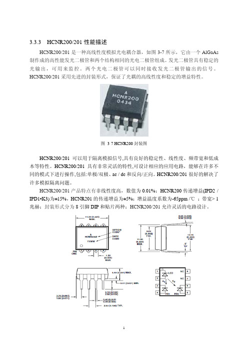
3.3.3 HCNR200/201性能描述HCNR200/201是一种高线性度模拟光电耦合器,如图3-7所示,它由一个AlGaAs 制作成的高性能发光二极管和两个结构相同的光电二极管组成。
发光二极管具有稳定的光输出,可用来监控。
两个光电二极管可以同时接收发光二极管输出的信号。
HCNR200/201采用先进的封装形式,保证了光耦的高线性度和稳定的增益特性。
图 3-7 HCNR200封装图HCNR200/201可以用于隔离模拟信号,具有良好的稳定性、线性度、频带宽和低成本等特性。
HCNR200/201具有非常灵活的特性,可设计相应的应用电路,能够在许多不同的模式下进行操作,包括:单极/双极、ac / dc和反向/正向。
HCNR200/201很好的解决了许多模拟隔离问题。
HCNR200/201产品特点有非线性度高,数值为0.01%;HCNR200传递增益(IPD2 / IPD1•K3)为±15%,HCNR201的传递增益为±5%;增益温度系数为-65ppm /℃;带宽> 1兆赫;封装形式分为8引脚DIP和贴片两种;HCNR200/201允许灵活的电路设计。
图 3-8 HCNR200内部管脚图HCNR200/201主要应用在低成本的模拟信号隔离、工业过程控制、电子反馈回路、监测电机电源电压、医疗等领域。
其内部结构图如图3-8所示。
图3-8说明了HCNR200/201是一种高线性度的光耦。
它由一个发光二极管(LED)和两个同种工艺的光电二极管组成。
其中一个光电二极管(PD1)在隔离电路的输入部分,另一个光电二极管(PD2)构成隔离电路的输出部分。
由于光耦的封装,使每一个光电二极管可从LED上接收大致相同数量的光线。
放大器与PD1组成的外部反馈电路可用来监控发光二极管(LED)发出的光,并且可以补充流过LED的电流起到对LED的调节作用。
使得LED输出的光信号更加稳定,当PD2接收到光信号后,可以再通过另一个运算放大器把接收到的电流信号转化为电压信号。
- 1、下载文档前请自行甄别文档内容的完整性,平台不提供额外的编辑、内容补充、找答案等附加服务。
- 2、"仅部分预览"的文档,不可在线预览部分如存在完整性等问题,可反馈申请退款(可完整预览的文档不适用该条件!)。
- 3、如文档侵犯您的权益,请联系客服反馈,我们会尽快为您处理(人工客服工作时间:9:00-18:30)。
2. 1基本测量原理
图2所示为用HCNR200实现一个简单隔离放大器的基本拓扑,除了光耦,还用了2个运放和2只电阻。
这个电路虽然简单,却清楚地解释了基本的隔离放大电路是如何工作的。
简单说来,为了维持运放A1的“+ ”输入端始终为0V,A1将不断地调整流过LED的电流If,进而决定PD1上的电流Ipd1。
比如,增大输入Vin,将引起A1“+ ”端电压升高,在正负端形成一个电压差,经过A1放大,输出电压增大, If随之增大,光强提高, Ipd1也随之增大,直至“+ ”端电压重新回到0V。
假定A1是理想运放,没有电流流入运放的输入端,所有流过R1的电流都流过PD1,在运放达到平衡后,有Ipd1=Vin/R1
图2基本拓扑
pd1仅仅决定于输入电压以及R1的值,与LED的输出光强特性无关,因此在输入电压与光电二极管的电流之间就建立起很好的线性关系。
另外,虽然LED的输出光强随着温度的变化而略受影响,但运放A1将通过调整If来进行补偿。
由于HCNR200特殊的封装结构, 2只光电二极管将得到近似的光强,有K= Ipd2/ Ipd1运放A2和电阻R2将Ipd2转换为电压输出,有Vout= pd23 R2
联立以上3式,得到输入输出电压的关系
V out/V
in= K3 (R2/R1)(2)
可以看出,Vout和Vin成线性关系,与LED的光强输
出特性无关。
并且仅仅通过调整R1和R2的值,就可以改变此隔离放大电路的增益。
图2是单极性输入电路,要求输入电压Vin必须为正。
改变LED、光电二极管或者运放正负输入端的接法,可以得到更多的适合不同场合的隔离放大电路,比如单极性负输入电路、双极性电路等。
2. 2电路硬件设计
图3中, 2只运放及周围阻容元件配合HCNR200构成了隔离电路,对电压较高的模拟量,可以进行分压。
同时,隔离两侧的供电要严格分开。
图中第一只运放及HCNR200 的LED和PD1部分采用+ A18V和模拟地(AGND)连接,第二只运放及HCNR200的PD2部分则由+ 18V和数字地( GND)相连,实现了电气隔离。
根据运放“虚短”和“虚断”
的特性,有
Ipd1=UAIN/R2
Ipd2=UAOUT/ (R4+R5/ /R6)
结合(1) ,得到UAOUT=UAIKR4+R5/ /R6R2(3)
可见,被测电压和输出电压之间存在正比的关系,只要适当选取电阻R2、R4、R5、R6的阻值,就可以得到一定比例的隔离输出电压。
图3高精度电压检测电路图
2. 3实验结果与分析
实际要求对4路0~10V电压, 1路0~40V电压以及1路0~60V电压进行隔离。
对于0~40V和0~60V模拟量,在第一只运放前加精密电阻进行分压,用200kΩ和100kΩ对0~40V 分压, 510kΩ和100kΩ对0~60V分压。
HCNR200的If要求在1mA~20mA之间,典型值为10mA,经过多次实验,证明R3取1kΩ比较合适;再根据Ipd的限制范围,取R2= 200kΩ。
理论上,若K =1,则有R4+ R5/ /R6= R2。
实验时,取R2=200kΩ。
UAIN从0逐渐增大到10V 测量输出端的电压UAOUT见表1 (电压单位为V) ,其中K为实际增益, K =UAOUT/UAIN。
表1实验结果
UAIN
U
AOUTKV
AIN
U
AOUTK
0.3490.3701.061085.2345.5551.06133
1.6061.7041.061025.8756.2351.06128
2.2482.3861.061396.5836.9851.06107
2.7792.9491.061177.0417.4751.06163
3.3733.5801.061377.5738.0361.06114
3.899
4.1371.061048.2298.7331.06124
4.6334.9171.061309.53310.1171.06126
可见,实际增益并不为1,取K = 1. 061进行修正,
则UAOUT=UAIN1. 061。
为提高精度,用电位器代替固定电阻R6,如图3
所示,对于每一路模拟量隔离,通过调整R6的大小,使UAOUT=UAIN,误差控制在毫伏级。
3总结
本文给出了运用高线性模拟光耦器件HCNR200实现模拟电压隔离的基本原理和硬件电路图。
合理选取电阻的大小,可以精确实现输入输出电压1∶1传输。
用本电路制成的模拟量隔离板在列车发电车检测中取得了理想的效果。
参考文献:
[1]张维.一种高精度信号调理电路[J ].自动化仪表, 2001,
(12) : 56 - 58.
[2]赵向华.一种实用的线性隔离检测电路[J ].电工技术杂
志, 2000, (10) : 24 - 25.
[3]陈本孝.微机监控系统中的V /F变换与隔离[J ].电测与仪
表, 1996, (7) : 12 - 14.
(许雪军编发)
—06—仪表技术2005年第5期。