MAX31865中文资料_数据手册_参数
MAXQ3181-RAN+;中文规格书,Datasheet资料

General Description The MAXQ3181 is a dedicated electricity measurementfront-end that collects and calculates polyphase volt-age, current, active power and energy, and many other metering parameters of a polyphase load. The comput-ed results can be retrieved by an external master through the on-chip serial peripheral interface (SPI™)bus. This bus is also used by the external master to configure the operation of the MAXQ3181 and monitor the status of operations.The MAXQ3181 performs voltage and current measure-ments using an integrated ADC that can measure up toseven external differential signal pairs. An eighth differ-ential signal pair is used to measure the die tempera-ture. An internal amplifier automatically adjusts the current channel gain to compensate for low-current channel-signal levels.Applications 3-Phase Active Energy Electricity Meters Features♦Compatible with 3-Phase/3-Wire, 3-Phase/4-Wire,and Other 3-Phase Services♦0.1% Active Power and Energy Linearity Error ♦0.5% Apparent Power and Energy Linearity Error ♦0.5% Linearity Errors for RMS Voltage and RMS Current♦Neutral Line Current Measurement♦Line Frequency (Hz)♦Power Factors♦Phase Sequence Indication♦Phase Voltage Absence Detection ♦Programmable Pulse Width♦Programmable No-Load Current Threshold♦Programmable Meter Constant♦Programmable Thresholds for Undervoltage andOvervoltage Detection♦Programmable Threshold for Overcurrent Detection♦Amp-Hours in Absence of Voltage Signals♦On-Chip Digital Temperature Sensor♦Precision Internal Voltage Reference 2.048V (30ppm/°C typical), Also Supports An ExternalVoltage Reference♦Active Power and Energy of Each Phase and Combined 3-Phase (kWh), Positive and Negative♦Apparent Power and Energy of Each Phase and Combined 3-Phase♦Supports Software Meter Calibration♦Up to 3-Point Multipoint Calibration to Compensate for Transducer Nonlinearity♦Power-Fail Detection♦Bidirectional Reset Input/Output♦SPI-Compatible Serial Interface with Interrupt Request (IRQ ) Output♦Single 3.3V Supply, Low Power (35mW typical)MAXQ3181Low-Power, Active Energy, Polyphase AFE ________________________________________________________________Maxim Integrated Products 119-4668; Rev 1; 12/09For pricing, delivery, and ordering information,please contact Maxim Direct at 1-888-629-4642,or visit Maxim’s website at .Note:Some revisions of this device may incorporate deviations from published specifications known as errata. Multiple revisions of any device may be simultaneously available through various sales channels. For information about device errata, go to: /errata .MAXQ is a registered trademark of Maxim Integrated Products, Inc.SPI is a trademark of Motorola, Inc.Ordering Information +Denotes a lead(Pb)-free/RoHS-compliant package.Pin Configuration and Typical Application Circuit appear atend of data sheet.M A X Q 3181Low-Power, Active Energy, Polyphase AFE 2_______________________________________________________________________________________Absolute Maximum Ratings . . . . . . . . . . . . . . . . . . . . . . . . . . . . . . . . . . . . . . . . . . . . . . . . . . . . . . . . . . . . . . . . . . . . . .8Metering Specifications . . . . . . . . . . . . . . . . . . . . . . . . . . . . . . . . . . . . . . . . . . . . . . . . . . . . . . . . . . . . . . . . . . . . . . . . .8Electrical Characteristics . . . . . . . . . . . . . . . . . . . . . . . . . . . . . . . . . . . . . . . . . . . . . . . . . . . . . . . . . . . . . . . . . . . . . . . .8SPI Slave Mode Timing . . . . . . . . . . . . . . . . . . . . . . . . . . . . . . . . . . . . . . . . . . . . . . . . . . . . . . . . . . . . . . . . . . . . . . . .10Block Diagram . . . . . . . . . . . . . . . . . . . . . . . . . . . . . . . . . . . . . . . . . . . . . . . . . . . . . . . . . . . . . . . . . . . . . . . . . . . . . . .11Pin Description . . . . . . . . . . . . . . . . . . . . . . . . . . . . . . . . . . . . . . . . . . . . . . . . . . . . . . . . . . . . . . . . . . . . . . . . . . . . . . .12Detailed Description . . . . . . . . . . . . . . . . . . . . . . . . . . . . . . . . . . . . . . . . . . . . . . . . . . . . . . . . . . . . . . . . . . . . . . . . . . .13Analog Front-End . . . . . . . . . . . . . . . . . . . . . . . . . . . . . . . . . . . . . . . . . . . . . . . . . . . . . . . . . . . . . . . . . . . . . . . . . .13Digital Signal Processor . . . . . . . . . . . . . . . . . . . . . . . . . . . . . . . . . . . . . . . . . . . . . . . . . . . . . . . . . . . . . . . . . . . . .13Precision Pulse Generators . . . . . . . . . . . . . . . . . . . . . . . . . . . . . . . . . . . . . . . . . . . . . . . . . . . . . . . . . . . . . . . . . . .13SPI Peripheral . . . . . . . . . . . . . . . . . . . . . . . . . . . . . . . . . . . . . . . . . . . . . . . . . . . . . . . . . . . . . . . . . . . . . . . . . . . . .13Operating Modes . . . . . . . . . . . . . . . . . . . . . . . . . . . . . . . . . . . . . . . . . . . . . . . . . . . . . . . . . . . . . . . . . . . . . . . . . .13Run Mode . . . . . . . . . . . . . . . . . . . . . . . . . . . . . . . . . . . . . . . . . . . . . . . . . . . . . . . . . . . . . . . . . . . . . . . . . . . . .13Stop Mode . . . . . . . . . . . . . . . . . . . . . . . . . . . . . . . . . . . . . . . . . . . . . . . . . . . . . . . . . . . . . . . . . . . . . . . . . . . .13Reset Sources . . . . . . . . . . . . . . . . . . . . . . . . . . . . . . . . . . . . . . . . . . . . . . . . . . . . . . . . . . . . . . . . . . . . . . . . . . . . .14External Reset . . . . . . . . . . . . . . . . . . . . . . . . . . . . . . . . . . . . . . . . . . . . . . . . . . . . . . . . . . . . . . . . . . . . . . . . . .14Power-On Reset . . . . . . . . . . . . . . . . . . . . . . . . . . . . . . . . . . . . . . . . . . . . . . . . . . . . . . . . . . . . . . . . . . . . . . . .15Watchdog Reset . . . . . . . . . . . . . . . . . . . . . . . . . . . . . . . . . . . . . . . . . . . . . . . . . . . . . . . . . . . . . . . . . . . . . . . .15Software Reset . . . . . . . . . . . . . . . . . . . . . . . . . . . . . . . . . . . . . . . . . . . . . . . . . . . . . . . . . . . . . . . . . . . . . . . . .15Power-Supply Monitoring . . . . . . . . . . . . . . . . . . . . . . . . . . . . . . . . . . . . . . . . . . . . . . . . . . . . . . . . . . . . . . . . .16Clock Sources . . . . . . . . . . . . . . . . . . . . . . . . . . . . . . . . . . . . . . . . . . . . . . . . . . . . . . . . . . . . . . . . . . . . . . . . . . . . .16External High-Frequency Crystal . . . . . . . . . . . . . . . . . . . . . . . . . . . . . . . . . . . . . . . . . . . . . . . . . . . . . . . . . . .16External High-Frequency Clock . . . . . . . . . . . . . . . . . . . . . . . . . . . . . . . . . . . . . . . . . . . . . . . . . . . . . . . . . . . .17Internal RC Oscillator . . . . . . . . . . . . . . . . . . . . . . . . . . . . . . . . . . . . . . . . . . . . . . . . . . . . . . . . . . . . . . . . . . . .17Master Communications . . . . . . . . . . . . . . . . . . . . . . . . . . . . . . . . . . . . . . . . . . . . . . . . . . . . . . . . . . . . . . . . . . . . .17SPI Communications Rate and Format . . . . . . . . . . . . . . . . . . . . . . . . . . . . . . . . . . . . . . . . . . . . . . . . . . . . . . .17SPI Communications Protocol . . . . . . . . . . . . . . . . . . . . . . . . . . . . . . . . . . . . . . . . . . . . . . . . . . . . . . . . . . . . .19Host Software Design . . . . . . . . . . . . . . . . . . . . . . . . . . . . . . . . . . . . . . . . . . . . . . . . . . . . . . . . . . . . . . . . . . . .22Register Set . . . . . . . . . . . . . . . . . . . . . . . . . . . . . . . . . . . . . . . . . . . . . . . . . . . . . . . . . . . . . . . . . . . . . . . . . . . . . . . . .22RAM-Based Registers . . . . . . . . . . . . . . . . . . . . . . . . . . . . . . . . . . . . . . . . . . . . . . . . . . . . . . . . . . . . . . . . . . . . . . . . .26General Operating Registers . . . . . . . . . . . . . . . . . . . . . . . . . . . . . . . . . . . . . . . . . . . . . . . . . . . . . . . . . . . . . . . . .26Global Status Register (STATUS) (0x000) . . . . . . . . . . . . . . . . . . . . . . . . . . . . . . . . . . . . . . . . . . . . . . . . . . . .26Operating Mode Register 0 (OPMODE0) (0x001) . . . . . . . . . . . . . . . . . . . . . . . . . . . . . . . . . . . . . . . . . . . . . .27Operating Mode Register 1 (OPMODE1) (0x002) . . . . . . . . . . . . . . . . . . . . . . . . . . . . . . . . . . . . . . . . . . . . . .27Operating Mode Register 2 (OPMODE2) (0x003) . . . . . . . . . . . . . . . . . . . . . . . . . . . . . . . . . . . . . . . . . . . . . .29TABLE OF CONTENTSMAXQ3181Low-Power, Active Energy, Polyphase AFE_______________________________________________________________________________________3Global Interrupt Registers . . . . . . . . . . . . . . . . . . . . . . . . . . . . . . . . . . . . . . . . . . . . . . . . . . . . . . . . . . . . . . . . . . . .31Interrupt Request Flag Register (IRQ_FLAG) (0x004) . . . . . . . . . . . . . . . . . . . . . . . . . . . . . . . . . . . . . . . . . . .31Interrupt Mask Register (IRQ_MASK) (0x006) . . . . . . . . . . . . . . . . . . . . . . . . . . . . . . . . . . . . . . . . . . . . . . . . .32Meter Pulse Configuration . . . . . . . . . . . . . . . . . . . . . . . . . . . . . . . . . . . . . . . . . . . . . . . . . . . . . . . . . . . . . . . . . . . . . .33Pulse Configuration—CFP Output (PLSCFG1) (0x01E) . . . . . . . . . . . . . . . . . . . . . . . . . . . . . . . . . . . . . . . . . . . . .33CFP Pulse Width (PLS1_WD) (0x020) . . . . . . . . . . . . . . . . . . . . . . . . . . . . . . . . . . . . . . . . . . . . . . . . . . . . . . . . . . .33CFP Pulse Threshold (THR1) (0x022) . . . . . . . . . . . . . . . . . . . . . . . . . . . . . . . . . . . . . . . . . . . . . . . . . . . . . . . . . . .34Calibration Registers . . . . . . . . . . . . . . . . . . . . . . . . . . . . . . . . . . . . . . . . . . . . . . . . . . . . . . . . . . . . . . . . . . . . . . . . . .34Current Gain, Phase X = A/B/C/N (X.I_GAIN) (A: 0x130, B: 0x21C, C: 0x308, N: 0x12E) . . . . . . . . . . . . . . . . . . .34Voltage Gain, Phase X = A/B/C (X.V_GAIN) (A: 0x132, B: 0x21E, C: 0x30A) . . . . . . . . . . . . . . . . . . . . . . . . . . . . .35Energy Gain, Phase X = A/B/C (X.E_GAIN) (A: 0x134, B: 0x220, C: 0x30C) . . . . . . . . . . . . . . . . . . . . . . . . . . . . .35Phase-Angle Compensation, High Range, Phase X = A/B/C (X.PA0) (A: 0x13E, B: 0x22A, C: 0x316) . . . . . . . . .35Phase-Angle Compensation, Medium Range, Phase X = A/B/C (X.PA1) (A: 0x140, B: 0x22C, C: 0x318) . . . . . .36Phase-Angle Compensation, Low Range, Phase X = A/B/C (X.PA2) (A: 0x142, B: 0x22E, C: 0x31A) . . . . . . . . .36Limit Registers . . . . . . . . . . . . . . . . . . . . . . . . . . . . . . . . . . . . . . . . . . . . . . . . . . . . . . . . . . . . . . . . . . . . . . . . . . . . . . .36Overcurrent Level (OCLVL) (0x044) . . . . . . . . . . . . . . . . . . . . . . . . . . . . . . . . . . . . . . . . . . . . . . . . . . . . . . . . . . . .36Overvoltage Level (OVLVL) (0x046) . . . . . . . . . . . . . . . . . . . . . . . . . . . . . . . . . . . . . . . . . . . . . . . . . . . . . . . . . . . .37Undervoltage Level (UVLVL) (0x048) . . . . . . . . . . . . . . . . . . . . . . . . . . . . . . . . . . . . . . . . . . . . . . . . . . . . . . . . . . .37No-Load Level (NOLOAD) (0x04A) . . . . . . . . . . . . . . . . . . . . . . . . . . . . . . . . . . . . . . . . . . . . . . . . . . . . . . . . . . . . .37Phase Status Registers . . . . . . . . . . . . . . . . . . . . . . . . . . . . . . . . . . . . . . . . . . . . . . . . . . . . . . . . . . . . . . . . . . . . . . . .38Interrupt Flags, Phase X = A/B/C (X.FLAGS) (A: 0x144, B: 0x230, C: 0x31C) . . . . . . . . . . . . . . . . . . . . . . . . . . . .38Interrupt Mask, Phase X = A/B/C (X.MASK) (A: 0x145, B: 0x231, C: 0x31D) . . . . . . . . . . . . . . . . . . . . . . . . . . . . .39Energy Overflow Flags, Phase X = A/B/C (X.EOVER) (A: 0x146, B: 0x232, C: 0x31E) . . . . . . . . . . . . . . . . . . . . .39Measurements . . . . . . . . . . . . . . . . . . . . . . . . . . . . . . . . . . . . . . . . . . . . . . . . . . . . . . . . . . . . . . . . . . . . . . . . . . . . . . .40Line Frequency (LINEFR) (0x062) . . . . . . . . . . . . . . . . . . . . . . . . . . . . . . . . . . . . . . . . . . . . . . . . . . . . . . . . . . . . . .40Power Factor, Phase X = A/B/C (X.PF) (A: 0x1C6, B: 0x2B2, C: 0x39E) . . . . . . . . . . . . . . . . . . . . . . . . . . . . . . . .40RMS Voltage, Phase X = A/B/C (X.VRMS) (A: 0x1C8, B: 0x2B4, C: 0x3A0) . . . . . . . . . . . . . . . . . . . . . . . . . . . . . .40RMS Current, Phase X = A/B/C (X.IRMS) (A: 0x1CC, B: 0x2B8, C: 0x3A4) . . . . . . . . . . . . . . . . . . . . . . . . . . . . . .41Energy, Real Positive, Phase X = A/B/C (X.EAPOS) (A: 0x1E8, B: 0x2D4, C: 0x3C0) . . . . . . . . . . . . . . . . . . . . . .41Energy, Real Negative, Phase X = A/B/C (X.EANEG) (A: 0x1EC, B: 0x2D8, C: 0x3C4) . . . . . . . . . . . . . . . . . . . . .42Energy, Apparent, Phase X = A/B/C (X.ES) (A: 0x1F8, B: 0x2E4, C: 0x3D0) . . . . . . . . . . . . . . . . . . . . . . . . . . . . .42Virtual Register Conversion Coefficients . . . . . . . . . . . . . . . . . . . . . . . . . . . . . . . . . . . . . . . . . . . . . . . . . . . . . . . . . . .43Voltage Units Conversion Coefficient (VOLT_CC) (0x014) . . . . . . . . . . . . . . . . . . . . . . . . . . . . . . . . . . . . . . . . . . .43Current Units Conversion Coefficient (AMP_CC) (0x016) . . . . . . . . . . . . . . . . . . . . . . . . . . . . . . . . . . . . . . . . . . . .43Power Units Conversion Coefficient (PWR_CC) (0x018) . . . . . . . . . . . . . . . . . . . . . . . . . . . . . . . . . . . . . . . . . . . . .44Energy Units Conversion Coefficient (ENR_CC) (0x01A) . . . . . . . . . . . . . . . . . . . . . . . . . . . . . . . . . . . . . . . . . . . .45TABLE OF CONTENTS (continued)M A X Q 3181Low-Power, Active Energy, Polyphase AFE 4_______________________________________________________________________________________Virtual Registers . . . . . . . . . . . . . . . . . . . . . . . . . . . . . . . . . . . . . . . . . . . . . . . . . . . . . . . . . . . . . . . . . . . . . . . . . . . . . .46Power . . . . . . . . . . . . . . . . . . . . . . . . . . . . . . . . . . . . . . . . . . . . . . . . . . . . . . . . . . . . . . . . . . . . . . . . . . . . . . . . . . . .46Real Power, Phase X = A/B/C/T (PWRP.X) (A: 0x801, B: 0x802, C: 0x804, T: 0x807) . . . . . . . . . . . . . . . . . . .46Apparent Power, Phase X = A/B/C/T (PWRS.X) (A: 0x821, B: 0x822, C: 0x824, T: 0x827) . . . . . . . . . . . . . . .46Voltage and Current . . . . . . . . . . . . . . . . . . . . . . . . . . . . . . . . . . . . . . . . . . . . . . . . . . . . . . . . . . . . . . . . . . . . . . . .47RMS Volts, Phase X = A/B/C (V.X) (A: 0x831, B: 0x832, C: 0x834) . . . . . . . . . . . . . . . . . . . . . . . . . . . . . . . . .47RMS Amps, Phase X = A/B/C/N (I.X) (A: 0x841, B: 0x842, C: 0x844, N: 0x840) . . . . . . . . . . . . . . . . . . . . . . .47Power Factor . . . . . . . . . . . . . . . . . . . . . . . . . . . . . . . . . . . . . . . . . . . . . . . . . . . . . . . . . . . . . . . . . . . . . . . . . . . . . .47Power Factor (PF.T) (0x867) . . . . . . . . . . . . . . . . . . . . . . . . . . . . . . . . . . . . . . . . . . . . . . . . . . . . . . . . . . . . . . .47Energy . . . . . . . . . . . . . . . . . . . . . . . . . . . . . . . . . . . . . . . . . . . . . . . . . . . . . . . . . . . . . . . . . . . . . . . . . . . . . . . . . .48Real Energy, Phase A/B/C/T (ENRP.X) (A: 0x8C1, B: 0x8C2, C: 0x8C4, T: 0x8C7) . . . . . . . . . . . . . . . . . . . . .48Apparent Energy, Phase A/B/C/T (ENRS.X) (A: 0x871, B: 0x872, C: 0x874, T: 0x877) . . . . . . . . . . . . . . . . . .48Theory of Operation . . . . . . . . . . . . . . . . . . . . . . . . . . . . . . . . . . . . . . . . . . . . . . . . . . . . . . . . . . . . . . . . . . . . . . . . . . .49Analog Front-End Operation . . . . . . . . . . . . . . . . . . . . . . . . . . . . . . . . . . . . . . . . . . . . . . . . . . . . . . . . . . . . . . . . . .49Digital Signal Processing (DSP) Terminology . . . . . . . . . . . . . . . . . . . . . . . . . . . . . . . . . . . . . . . . . . . . . . . . . . . . .49Digital Processing . . . . . . . . . . . . . . . . . . . . . . . . . . . . . . . . . . . . . . . . . . . . . . . . . . . . . . . . . . . . . . . . . . . . . . . . . .49Per Sample Operations . . . . . . . . . . . . . . . . . . . . . . . . . . . . . . . . . . . . . . . . . . . . . . . . . . . . . . . . . . . . . . . . . . . . . .50Per DSP Cycle Operations . . . . . . . . . . . . . . . . . . . . . . . . . . . . . . . . . . . . . . . . . . . . . . . . . . . . . . . . . . . . . . . . . . .50Energy Accumulation . . . . . . . . . . . . . . . . . . . . . . . . . . . . . . . . . . . . . . . . . . . . . . . . . . . . . . . . . . . . . . . . . . . . . . .52No-Zero-Crossing Detection . . . . . . . . . . . . . . . . . . . . . . . . . . . . . . . . . . . . . . . . . . . . . . . . . . . . . . . . . . . . . . . . . .52Phase Sequence Status . . . . . . . . . . . . . . . . . . . . . . . . . . . . . . . . . . . . . . . . . . . . . . . . . . . . . . . . . . . . . . . . . . . . .52Power Calculation (Active and Apparent) . . . . . . . . . . . . . . . . . . . . . . . . . . . . . . . . . . . . . . . . . . . . . . . . . . . . . . . .53Energy Accumulation Start Delay . . . . . . . . . . . . . . . . . . . . . . . . . . . . . . . . . . . . . . . . . . . . . . . . . . . . . . . . . . . . . .53No-Load Feature . . . . . . . . . . . . . . . . . . . . . . . . . . . . . . . . . . . . . . . . . . . . . . . . . . . . . . . . . . . . . . . . . . . . . . . . . . .53On Demand Calculations . . . . . . . . . . . . . . . . . . . . . . . . . . . . . . . . . . . . . . . . . . . . . . . . . . . . . . . . . . . . . . . . . . . .53RMS Volts, RMS Amps . . . . . . . . . . . . . . . . . . . . . . . . . . . . . . . . . . . . . . . . . . . . . . . . . . . . . . . . . . . . . . . . . . .53Power . . . . . . . . . . . . . . . . . . . . . . . . . . . . . . . . . . . . . . . . . . . . . . . . . . . . . . . . . . . . . . . . . . . . . . . . . . . . . . . .54Power Factor . . . . . . . . . . . . . . . . . . . . . . . . . . . . . . . . . . . . . . . . . . . . . . . . . . . . . . . . . . . . . . . . . . . . . . . . . . .54Line Frequency . . . . . . . . . . . . . . . . . . . . . . . . . . . . . . . . . . . . . . . . . . . . . . . . . . . . . . . . . . . . . . . . . . . . . . . .54Energy . . . . . . . . . . . . . . . . . . . . . . . . . . . . . . . . . . . . . . . . . . . . . . . . . . . . . . . . . . . . . . . . . . . . . . . . . . . . . . . .54Meter Pulse . . . . . . . . . . . . . . . . . . . . . . . . . . . . . . . . . . . . . . . . . . . . . . . . . . . . . . . . . . . . . . . . . . . . . . . . . . . . . . .55Generating Pulses . . . . . . . . . . . . . . . . . . . . . . . . . . . . . . . . . . . . . . . . . . . . . . . . . . . . . . . . . . . . . . . . . . . . . . . . . .55Meter Constant . . . . . . . . . . . . . . . . . . . . . . . . . . . . . . . . . . . . . . . . . . . . . . . . . . . . . . . . . . . . . . . . . . . . . . . . . . . .55Interrupts . . . . . . . . . . . . . . . . . . . . . . . . . . . . . . . . . . . . . . . . . . . . . . . . . . . . . . . . . . . . . . . . . . . . . . . . . . . . . .55Overvoltage and Overcurrent Detection . . . . . . . . . . . . . . . . . . . . . . . . . . . . . . . . . . . . . . . . . . . . . . . . . . . . . .56Meter Units to Real Units Conversion . . . . . . . . . . . . . . . . . . . . . . . . . . . . . . . . . . . . . . . . . . . . . . . . . . . . . . . . . . .56Units Conversion Examples . . . . . . . . . . . . . . . . . . . . . . . . . . . . . . . . . . . . . . . . . . . . . . . . . . . . . . . . . . . . . . . . . .58TABLE OF CONTENTS (continued)MAXQ3181Low-Power, Active Energy, Polyphase AFE _______________________________________________________________________________________5Calibration Procedure . . . . . . . . . . . . . . . . . . . . . . . . . . . . . . . . . . . . . . . . . . . . . . . . . . . . . . . . . . . . . . . . . . . . . . . . .58Calibration Overview . . . . . . . . . . . . . . . . . . . . . . . . . . . . . . . . . . . . . . . . . . . . . . . . . . . . . . . . . . . . . . . . . . . . . . . .58Calibrating Voltage . . . . . . . . . . . . . . . . . . . . . . . . . . . . . . . . . . . . . . . . . . . . . . . . . . . . . . . . . . . . . . . . . . . . . . . . .59Calibrating Current . . . . . . . . . . . . . . . . . . . . . . . . . . . . . . . . . . . . . . . . . . . . . . . . . . . . . . . . . . . . . . . . . . . . . . . . .59Calibrating Phase Offset . . . . . . . . . . . . . . . . . . . . . . . . . . . . . . . . . . . . . . . . . . . . . . . . . . . . . . . . . . . . . . . . . . . . .60Interfacing the MAXQ3181 to External Hardware . . . . . . . . . . . . . . . . . . . . . . . . . . . . . . . . . . . . . . . . . . . . . . . . . . . .60Connections to the Power Source . . . . . . . . . . . . . . . . . . . . . . . . . . . . . . . . . . . . . . . . . . . . . . . . . . . . . . . . . . . . . .61Sensor Selection . . . . . . . . . . . . . . . . . . . . . . . . . . . . . . . . . . . . . . . . . . . . . . . . . . . . . . . . . . . . . . . . . . . . . . . . . . . . .61Voltage Sensors . . . . . . . . . . . . . . . . . . . . . . . . . . . . . . . . . . . . . . . . . . . . . . . . . . . . . . . . . . . . . . . . . . . . . . . . . . .61Voltage-Divider . . . . . . . . . . . . . . . . . . . . . . . . . . . . . . . . . . . . . . . . . . . . . . . . . . . . . . . . . . . . . . . . . . . . . . . . .61Voltage Transformer . . . . . . . . . . . . . . . . . . . . . . . . . . . . . . . . . . . . . . . . . . . . . . . . . . . . . . . . . . . . . . . . . . . . .61Current Sensors . . . . . . . . . . . . . . . . . . . . . . . . . . . . . . . . . . . . . . . . . . . . . . . . . . . . . . . . . . . . . . . . . . . . . . . . . . . .62Current Shunt . . . . . . . . . . . . . . . . . . . . . . . . . . . . . . . . . . . . . . . . . . . . . . . . . . . . . . . . . . . . . . . . . . . . . . . . . .62Current Transformer . . . . . . . . . . . . . . . . . . . . . . . . . . . . . . . . . . . . . . . . . . . . . . . . . . . . . . . . . . . . . . . . . . . . .62Advanced Operation . . . . . . . . . . . . . . . . . . . . . . . . . . . . . . . . . . . . . . . . . . . . . . . . . . . . . . . . . . . . . . . . . . . . . . . . . .62Modifying the ADC Operation . . . . . . . . . . . . . . . . . . . . . . . . . . . . . . . . . . . . . . . . . . . . . . . . . . . . . . . . . . . . . . . . .62Fine-Tuning the DSP Controls . . . . . . . . . . . . . . . . . . . . . . . . . . . . . . . . . . . . . . . . . . . . . . . . . . . . . . . . . . . . . . . . .62Fine-Tuning the Line Frequency Measurement . . . . . . . . . . . . . . . . . . . . . . . . . . . . . . . . . . . . . . . . . . . . . . . .62Low-Power Measurement Mode (LOWPM) . . . . . . . . . . . . . . . . . . . . . . . . . . . . . . . . . . . . . . . . . . . . . . . . . . . . . . .63Temperature . . . . . . . . . . . . . . . . . . . . . . . . . . . . . . . . . . . . . . . . . . . . . . . . . . . . . . . . . . . . . . . . . . . . . . . . . . . . . .63Advanced Calibrations . . . . . . . . . . . . . . . . . . . . . . . . . . . . . . . . . . . . . . . . . . . . . . . . . . . . . . . . . . . . . . . . . . . . . .63Calibrating Current Offset . . . . . . . . . . . . . . . . . . . . . . . . . . . . . . . . . . . . . . . . . . . . . . . . . . . . . . . . . . . . . . . . .63Calibrating Linearity . . . . . . . . . . . . . . . . . . . . . . . . . . . . . . . . . . . . . . . . . . . . . . . . . . . . . . . . . . . . . . . . . . . . .63Calibrating Power/Energy Gain . . . . . . . . . . . . . . . . . . . . . . . . . . . . . . . . . . . . . . . . . . . . . . . . . . . . . . . . . . . .64Multipoint Phase Offset Calibration . . . . . . . . . . . . . . . . . . . . . . . . . . . . . . . . . . . . . . . . . . . . . . . . . . . . . . . . .64Advanced Register Configurations . . . . . . . . . . . . . . . . . . . . . . . . . . . . . . . . . . . . . . . . . . . . . . . . . . . . . . . . . . . . . . .65Analog Scan Configuration Registers . . . . . . . . . . . . . . . . . . . . . . . . . . . . . . . . . . . . . . . . . . . . . . . . . . . . . . . . . . .65Time Slot Assignment—Current Channel X = A/B/C (SCAN_IX) (A: 0x008, B: 0x00C, C: 0x00A) . . . . . . . . . .65Time Slot Assignment—Voltage Channel X = A/B/C (SCAN_VX) (A: 0x009, B: 0x00D, C: 0x00B) . . . . . . . . .66Time Slot Assignment—Neutral Current Channel (SCAN_IN) (0x00E) . . . . . . . . . . . . . . . . . . . . . . . . . . . . . . .67Time Slot Assignment—Temperature Channel (SCAN_TE) (0x00F) . . . . . . . . . . . . . . . . . . . . . . . . . . . . . . . .68Neutral Current . . . . . . . . . . . . . . . . . . . . . . . . . . . . . . . . . . . . . . . . . . . . . . . . . . . . . . . . . . . . . . . . . . . . . . . . . . . .69Auxiliary Channel Configuration (AUX_CFG) (0x010) . . . . . . . . . . . . . . . . . . . . . . . . . . . . . . . . . . . . . . . . . . .69DSP System Configuration . . . . . . . . . . . . . . . . . . . . . . . . . . . . . . . . . . . . . . . . . . . . . . . . . . . . . . . . . . . . . . . . . . .69System Clock Frequency (SYS_KHZ) (0x012) . . . . . . . . . . . . . . . . . . . . . . . . . . . . . . . . . . . . . . . . . . . . . . . . .69Cycle Count (CYCNT) (0x01C) . . . . . . . . . . . . . . . . . . . . . . . . . . . . . . . . . . . . . . . . . . . . . . . . . . . . . . . . . . . . .70Number of Scan Frames per DSP Cycle (NS) (0x040) . . . . . . . . . . . . . . . . . . . . . . . . . . . . . . . . . . . . . . . . . . .70TABLE OF CONTENTS (continued)M A X Q 3181Low-Power, Active Energy, Polyphase AFE 6_______________________________________________________________________________________Filter Coefficients . . . . . . . . . . . . . . . . . . . . . . . . . . . . . . . . . . . . . . . . . . . . . . . . . . . . . . . . . . . . . . . . . . . . . . . . . . .71Line Cycle Noise Rejection Filter (REJ_NS) (0x02C) . . . . . . . . . . . . . . . . . . . . . . . . . . . . . . . . . . . . . . . . . . . .71Line Cycle Averaging Filter (AVG_NS) (0x02E) . . . . . . . . . . . . . . . . . . . . . . . . . . . . . . . . . . . . . . . . . . . . . . . .71Meter Measurement Averaging Filter (AVG_C) (0x030) . . . . . . . . . . . . . . . . . . . . . . . . . . . . . . . . . . . . . . . . . .72Meter Measurement Highpass Filter (HPF_C) (0x032) . . . . . . . . . . . . . . . . . . . . . . . . . . . . . . . . . . . . . . . . . . .72Zero-Cross Lowpass Filter (ZC_LPF) (0x05A) . . . . . . . . . . . . . . . . . . . . . . . . . . . . . . . . . . . . . . . . . . . . . . . . .72Hardware Mirror Registers . . . . . . . . . . . . . . . . . . . . . . . . . . . . . . . . . . . . . . . . . . . . . . . . . . . . . . . . . . . . . . . . . . .73ADC Configuration (R_ACFG) (0x04C) . . . . . . . . . . . . . . . . . . . . . . . . . . . . . . . . . . . . . . . . . . . . . . . . . . . . . . .73ADC Conversion Rate (R_ADCRATE) (0x04E) . . . . . . . . . . . . . . . . . . . . . . . . . . . . . . . . . . . . . . . . . . . . . . . . .73ADC Settling Time (R_ADCACQ) (0x050) . . . . . . . . . . . . . . . . . . . . . . . . . . . . . . . . . . . . . . . . . . . . . . . . . . . .74SPI Configuration (R_SPICF) (0x052) . . . . . . . . . . . . . . . . . . . . . . . . . . . . . . . . . . . . . . . . . . . . . . . . . . . . . . . .74Timeouts . . . . . . . . . . . . . . . . . . . . . . . . . . . . . . . . . . . . . . . . . . . . . . . . . . . . . . . . . . . . . . . . . . . . . . . . . . . . . . . . .75Zero-Crossing Timeout (NZX_TIMO) (0x054) . . . . . . . . . . . . . . . . . . . . . . . . . . . . . . . . . . . . . . . . . . . . . . . . . .75Communications Timeout (COM_TIMO) (0x056) . . . . . . . . . . . . . . . . . . . . . . . . . . . . . . . . . . . . . . . . . . . . . . .75Energy Accumulation Timeout (ACC_TIMO) (0x058) . . . . . . . . . . . . . . . . . . . . . . . . . . . . . . . . . . . . . . . . . . . .75Phase-Angle Compensation . . . . . . . . . . . . . . . . . . . . . . . . . . . . . . . . . . . . . . . . . . . . . . . . . . . . . . . . . . . . . . . . . .76Phase Offset Current Threshold 1 (I1THR) (0x05C) . . . . . . . . . . . . . . . . . . . . . . . . . . . . . . . . . . . . . . . . . . . . .76Phase Offset Current Threshold 2 (I2THR) (0x05E) . . . . . . . . . . . . . . . . . . . . . . . . . . . . . . . . . . . . . . . . . . . . .76Miscellaneous Gain . . . . . . . . . . . . . . . . . . . . . . . . . . . . . . . . . . . . . . . . . . . . . . . . . . . . . . . . . . . . . . . . . . . . . . . . .76Neutral Current Gain (N.I_GAIN) (0x12E) . . . . . . . . . . . . . . . . . . . . . . . . . . . . . . . . . . . . . . . . . . . . . . . . . . . . .76Linearity Compensation . . . . . . . . . . . . . . . . . . . . . . . . . . . . . . . . . . . . . . . . . . . . . . . . . . . . . . . . . . . . . . . . . . . . . .77Linearity Offset, High Range, Phase X = A/B/C (X.OFFS_HI) (A: 0x138, B: 0x224, C: 0x310) . . . . . . . . . . . . .77Linearity Gain Coefficient, Low Range, Phase X = A/B/C (X.GAIN_LO) (A: 0x13A, B: 0x226, C: 0x312) . . . .77Linearity Offset, Low Range, Phase X = A/B/C (X.OFFS_LO) (A: 0x13C, B: 0x228, C: 0x314) . . . . . . . . . . . .78Measurements—RAM Registers . . . . . . . . . . . . . . . . . . . . . . . . . . . . . . . . . . . . . . . . . . . . . . . . . . . . . . . . . . . . . . . . .78On-Demand RMS Result (N.IRMS) (0x11C) . . . . . . . . . . . . . . . . . . . . . . . . . . . . . . . . . . . . . . . . . . . . . . . . . . . . . .78Energy Accumulated in the Last DSP Cycle . . . . . . . . . . . . . . . . . . . . . . . . . . . . . . . . . . . . . . . . . . . . . . . . . . . . . .79Real Energy, Phase X = A/B/C (X.ACT) (A: 0x1D0, B: 0x2BC, C: 0x3A8) . . . . . . . . . . . . . . . . . . . . . . . . . . . .79Apparent Energy, Phase X = A/B/C (X.APP) (A: 0x1D8, B: 0x2C4, C: 0x3B0) . . . . . . . . . . . . . . . . . . . . . . . . .79Checksum (CHKSUM) (0x060) . . . . . . . . . . . . . . . . . . . . . . . . . . . . . . . . . . . . . . . . . . . . . . . . . . . . . . . . . . . . . . . .80Neutral Current . . . . . . . . . . . . . . . . . . . . . . . . . . . . . . . . . . . . . . . . . . . . . . . . . . . . . . . . . . . . . . . . . . . . . . . . . . . .81RMS Current, Neutral (I.N) (0x840) . . . . . . . . . . . . . . . . . . . . . . . . . . . . . . . . . . . . . . . . . . . . . . . . . . . . . . . . . .81Special Commands . . . . . . . . . . . . . . . . . . . . . . . . . . . . . . . . . . . . . . . . . . . . . . . . . . . . . . . . . . . . . . . . . . . . . . . . .81Applications Information . . . . . . . . . . . . . . . . . . . . . . . . . . . . . . . . . . . . . . . . . . . . . . . . . . . . . . . . . . . . . . . . . . . . . . .81Grounds and Bypassing . . . . . . . . . . . . . . . . . . . . . . . . . . . . . . . . . . . . . . . . . . . . . . . . . . . . . . . . . . . . . . . . . . . . .81Specific Design Considerations for MAXQ3181-Based Systems . . . . . . . . . . . . . . . . . . . . . . . . . . . . . . . . . . . . . .81Additional Documentation . . . . . . . . . . . . . . . . . . . . . . . . . . . . . . . . . . . . . . . . . . . . . . . . . . . . . . . . . . . . . . . . . . . .82TABLE OF CONTENTS (continued)。
MAX3465ESD-T中文资料

or Noisy Bus Lines ♦ Full-Duplex and Half-Duplex Versions Available ♦ Phase Controls to Correct for Twisted-Pair
Features
♦ Recommended for Profibus Applications ♦ Up to 40Mbps Data Rate ♦ 15ns Transmitter Propagation Delay ♦ 20ns Receiver Propagation Delay ♦ 2ns Transmitter and Receiver Skew ♦ High Differential Driver Output Level (2.1V on 54Ω) ♦ Hot-Swap Versions ♦ 1µA Shutdown Supply Current ♦ Low Supply Current Requirements (2.5mA, typ) ♦ Allow Up to 128 Transceivers on the Bus ♦ True Fail-Safe Receiver while Maintaining EIA/TIA-
Ordering Information
PART
TEMP RANGE PIN-PACKAGE
MAX3465CSD
0°C to +70°C 14 SO
MAX3465CPD
0°C to +70°C 14 Plastic DIP
MAX3465ESD
-40°C to +85°C 14 SO
MAX3185CWP+T中文资料

_______________General DescriptionThe MAX3185 is a complete DTE RS-232 serial port designed to meet the stringent ESD requirements of the European community. All transmitter outputs and receiv-er inputs are protected to ±15kV using IEC 1000-4-2 Air-Gap Discharge, ±8kV using IEC 1000-4-2 Contact Discharge, and ±15kV using the Human Body Model.The MAX3185 has three RS-232 transmitters, five RS-232 receivers, and no charge pump, optimizing it for operation in desktop PC and motherboard applications.It is guaranteed to run at data rates up to 230kbps, pro-viding compatibility with popular software for communi-cating with personal computers. Power-supply current is less than 300µA for I DD and I SS , and less than 1mA for I CC .The MAX3185 is pin and functionally compatible with the industry-standard 75185, so existing designs can instantly become EMC compliant. The MAX3185 is available in an SO package and in the tiny SSOP that further reduces board space.________________________ApplicationsDesktop PC Motherboards InstrumentsEquipment Meeting IEC1000-4-2____________________________Featureso Enhanced ESD Protection:±15kV—Human Body Model±8kV—IEC1000-4-2, Contact Discharge ±15kV—IEC1000-4-2, Air-Gap Discharge o Latchup Free During an ESD Event o 20-Pin SSOP and SO Packages o Guaranteed 230kbps Data Rate o Flow-Through Pinouto Pin Compatible with SN75C185o Complete DTE Serial PortMAX3185±15kV ESD-Protected, EMC-Compliant, 230kbps RS-232 Serial Port for Motherboards/Desktop PCs________________________________________________________________Maxim Integrated Products 1__________________Pin Configuration__________Typical Operating Circuit19-1076; Rev 0; 9/96______________Ordering InformationFor free samples & the latest literature: , or phone 1-800-998-8800M A X 3185±15kV ESD-Protected, EMC-Compliant, 230kbps RS-232 Serial Port for Motherboards/Desktop PCsABSOLUTE MAXIMUM RATINGSELECTRICAL CHARACTERISTICS(V CC = +4.5V to +5.5V, V DD = +10.8V to +13.2V, V SS = -10.8V to -13.2V, T A = T MIN to T MAX , unless otherwise noted. Typical values Stresses beyond those listed under “Absolute Maximum Ratings” may cause permanent damage to the device. These are stress ratings only, and functional operation of the device at these or any other conditions beyond those indicated in the operational sections of the specifications is not implied. Exposure to absolute maximum rating conditions for extended periods may affect device reliability.V CC ...........................................................................-0.3V to +7V V DD .........................................................................-0.3V to +14V V SS .........................................................................+0.3V to -14V Input VoltagesT IN ........................................................................-0.3V to +6V R IN ...................................................................................±30V Output VoltagesT OUT .................................................................................±15V R OUT .......................................................-0.3V to (V CC + 0.3V)Short-Circuit DurationT OUT (one at a time)...............................................Continuous R OUT (one at a time)..............................................ContinuousContinuous Power Dissipation (T A = +70°C)Wide SO (derate 10.00mW/°C above +70°C)..............800mW SSOP (derate 8.00mW/°C above +70°C)....................640mW Operating Temperature RangesMAX3185C_ P.....................................................0°C to +70°C MAX3185E_ P..................................................-40°C to +85°C Storage Temperature Range ............................-65°C to +160°C Lead Temperature (soldering, 10sec) ............................+300°CMAX3185±15kV ESD-Protected, EMC-Compliant, 230kbps RS-232 Serial Port for Motherboards/Desktop PCs_______________________________________________________________________________________3ELECTRICAL CHARACTERISTICS (continued)(V CC = +4.5V to +5.5V, V DD = +10.8V to +13.2V, V SS = -10.8V to -13.2V, T A = T MIN to T MAX , unless otherwise noted. Typical values are at T A = +25°C.)M A X 3185±15kV ESD-Protected, EMC-Compliant, 230kbps RS-232 Serial Port for Motherboards/Desktop PCs 4_________________________________________________________________________________________________________________________________Typical Operating Characteristics(V CC = +5.0V, V DD = +12.0V, V SS = -12.0V, T A = +25°C, unless otherwise noted.)-20SUPPLY CURRENT vs. SUPPLY VOLTAGESUPPLY VOLTAGE (V)S U P P L Y C U R E E N T (m A )-15-10-50510152013.212.612.011.410.8SUPPLY CURRENT vs. LOAD CAPACITANCELOAD CAPACITANCE (pF)S U P P L Y C U R E E N T (m A )2520151050-5-10-15-20-25400050003000200010000SLEW RATEvs. LOAD CAPACITANCELOAD CAPACITANCE (pF)S L E W R A T E (V /µs )1614121086420400050003000200010000TRANSMITTER OUTPUT VOLTAGEvs. LOAD CAPACITANCELOAD CAPACITANCE (pF)T R A N S M I T T E R O U T P U T V O L T A G E (V )400050003000200010000MAX3185 TRANSMITTER OUTPUT VOLTAGE vs. LOAD CURRENT PER TRANSMITTERLOAD CURRENT PER TRANSMITTER (mA)T R A N S M I T T E R O U T P U T V O L T A G E (V )101214161868240SLEW RATE vs. TEMPERATURETEMPERATURE (°C)S L E W R A T E (V /µs )2520151050851051254565525-35-15-55_______________Detailed Description±15kV ESD ProtectionAs with all Maxim devices, ESD-protection structures are incorporated on all pins to protect against electro-static discharges encountered during handling and assembly. The MAX3185 driver outputs and receiver inputs have extra protection against static electricity found in normal operation. Maxim’s engineers devel-oped state-of-the-art structures to protect these pins against ESD of ±15kV, without damage. After an ESD event, the MAX3185 continues working without latchup.ESD protection can be tested in several ways. The transmitter outputs and the receiver inputs are charac-terized for protection to the following:1)±15kV using the Human Body Model2)±8kV using the Contact-Discharge Method specified in IEC1000-4-2 (formerly IEC801-2)3)±15kV using the Air-Gap Method specified in IEC1000-4-2 (formerly IEC801-2)ESD Test ConditionsESD performance depends on a number of conditions.Contact Maxim for a reliability report that documents test setup, methodology, and results.MAX3185±15kV ESD-Protected, EMC-Compliant, 230kbps RS-232 Serial Port for Motherboards/Desktop PCs_______________________________________________________________________________________5______________________________________________________________Pin DescriptionPIN NAME FUNCTION1V DDSupply-Voltage Input, +10.8V to +13.2V 12, 14, 17, 18, 19R5OUT–R1OUT Receiver Outputs, swing between GND and V CC 16, 15, 13T3IN, T2IN, T1INTransmitter Inputs10V SS Supply-Voltage Input, -10.8V to -13.2V 11GND Ground. Connect system to ground.2, 3, 4, 7, 9R1IN–R5IN Receiver Inputs5, 6, 8T1OUT, T2OUT, T3OUTTransmitter Outputs, swing between V DD and V SS 20V CCSupply-Voltage Input, +4.5V to +5.5VFigure 1a. IEC1000-4-2 ESD Test ModelFigure 1b. IEC1000-4-2 ESD-Generator Current WaveformHuman Body ModelFigure 2a shows the Human Body Model, and Figure 2b shows the current waveform it generates when dis-charged into a low impedance. This model consists of a 100pF capacitor charged to the ESD voltage of inter-est, which is then discharged into the device through a 1.5k Ωresistor.IEC1000-4-2The IEC1000-4-2 standard covers ESD testing and per-formance of finished equipment; it does not specifically refer to integrated circuits. The MAX3185 helps you design equipment that meets Level 4 (the highest level)of IEC1000-4-2, without additional ESD-protection com-ponents.The main difference between tests done using the Human Body Model and IEC1000-4-2 is higher peak current in IEC1000-4-2. Because series resistance is lower in the IEC1000-4-2 ESD test model (Figure 1a),the ESD withstand voltage measured to this standard is generally lower than that measured using the Human Body Model. Figure 1b shows the current waveform for the ±8kV IEC1000-4-2 Level 4 ESD Contact-Discharge test.The Air-Gap test involves approaching the device with a charge probe. The Contact-Discharge method connects the probe to the device before the probe is energized.Machine ModelThe Machine Model for ESD testing uses a 200pF stor-age capacitor and zero-discharge resistance. It mimics the stress caused by handling during manufacturing and assembly. Of course, all pins (not just RS-232inputs and outputs) require this protection during man-ufacturing. Therefore, the Machine Model is less rele-vant to the I/O ports than are the Human Body Model and IEC1000-4-2.__________Applications InformationUse proper layout to ensure other devices on your board are not damaged in an ESD strike. Currents as high as 60A can instantaneously pass into ground, so be sure to minimize the ground-lead return path to the power supply. A separate return path to the power sup-ply is recommend. Trace widths should be greater than 40 mils. Bypass V CC , V DD , and V SS with 0.1µF capaci-tors as close to the part as possible to ensure maxi-mum ESD protection.Tie any unused transmitter inputs to GND or V CC . No external protection diodes are needed because the MAX3185 is not sensitive to power-supply sequencing.M A X 3185±15kV ESD-Protected, EMC-Compliant, 230kbps RS-232 Serial Port for Motherboards/Desktop PCs 6_______________________________________________________________________________________Figure 2a. Human Body ESD Test Model Figure 2b. Human Body Model Current WaveformMAX3185±15kV ESD-Protected, EMC-Compliant, 230kbps RS-232 Serial Port for Motherboards/Desktop PCs_______________________________________________________________________________________7TRANSISTOR COUNT: 217___________________Chip InformationFigure 3. Slew-Rate Test Circuit and Timing DiagramM A X 3185±15kV ESD-Protected, EMC-Compliant, 230kbps RS-232 Serial Port for Motherboards/Desktop PCs implied. Maxim reserves the right to change the circuitry and specifications without notice at any time.8___________________Maxim Integrated Products, 120 San Gabriel Drive, Sunnyvale, CA 94086 (408) 737-7600©1996 Maxim Integrated ProductsPrinted USAis a registered trademark of Maxim Integrated Products.________________________________________________________Package Information。
MAX6385XS33D7-T中文资料
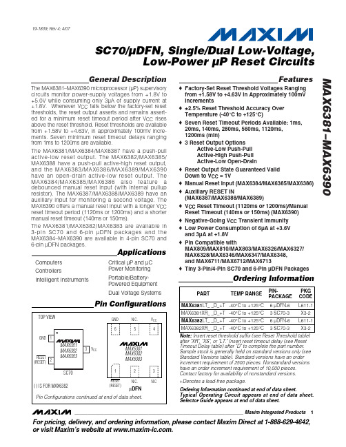
General Description The MAX6381–MAX6390 microprocessor (µP) supervisory circuits monitor power-supply voltages from +1.8V to +5.0V while consuming only 3µA of supply current at +1.8V. Whenever V CC falls below the factory-set reset thresholds, the reset output asserts and remains assert-ed for a minimum reset timeout period after V CC rises above the reset threshold. Reset thresholds are available from +1.58V to +4.63V, in approximately 100mV incre-ments. Seven minimum reset timeout delays ranging from 1ms to 1200ms are available.The MAX6381/MAX6384/MAX6387 have a push-pull active-low reset output. The MAX6382/MAX6385/ MAX6388 have a push-pull active-high reset output, and the MAX6383/MAX6386/MAX6389/MAX6390 have an open-drain active-low reset output. The MAX6384/MAX6385/MAX6386 also feature a debounced manual reset input (with internal pullup resistor). The MAX6387/MAX6388/MAX6389 have an auxiliary input for monitoring a second voltage. The MAX6390 offers a manual reset input with a longer V CC reset timeout period (1120ms or 1200ms) and a shorter manual reset timeout (140ms or 150ms).The MAX6381/MAX6382/MAX6383 are available in 3-pin SC70 and6-pinµDFN packages and the MAX6384–MAX6390 are available in 4-pin SC70 andFeatures♦Factory-Set Reset Threshold Voltages Rangingfrom +1.58V to +4.63V in Approximately 100mVIncrements♦±2.5% Reset Threshold Accuracy OverTemperature (-40°C to +125°C)♦Seven Reset Timeout Periods Available: 1ms,20ms, 140ms, 280ms, 560ms, 1120ms,1200ms (min)♦3 Reset Output OptionsActive-Low Push-PullActive-High Push-PullActive-Low Open-Drain♦Reset Output State Guaranteed ValidDown to V CC= 1V♦Manual Reset Input (MAX6384/MAX6385/MAX6386)♦Auxiliary RESET IN(MAX6387/MAX6388/MAX6389)♦V CC Reset Timeout (1120ms or 1200ms)/ManualReset Timeout (140ms or 150ms) (MAX6390)♦Negative-Going V CC Transient Immunity♦Low Power Consumption of 6µA at +3.6Vand 3µA at +1.8V♦Pin Compatible withMAX809/MAX810/MAX803/MAX6326/MAX6327/MAX6328/MAX6346/MAX6347/MAX6348,and MAX6711/MAX6712/MAX6713♦Tiny 3-Pin/4-Pin SC70 and 6-Pin µDFN PackagesMAX6381–MAX6390 SC70/µDFN, Single/Dual Low-Voltage,Low-Power µP Reset Circuits ________________________________________________________________Maxim Integrated Products1Pin Configurations19-1839; Rev 4; 4/07Ordering InformationOrdering Information continued at end of data sheet.Typi cal Operati ng Ci rcui t appears at end of data sheet.Selector Guide appears at end of data sheet.after "XR", "XS", or "LT." Insert reset timeout delay (see ResetTimeout Delay table) after "D" to complete the part number.Sample stock is generally held on standard versions only (seeStandard Versions table). Standard versions have an orderincrement requirement of 2500 pieces. Nonstandard versionshave an order increment requirement of 10,000 pieces.Contact factory for availability of nonstandard versions.+Denotes a lead-free package.For pricing, delivery, and ordering information,please contact Maxim Direct at 1-888-629-4642,or visit Maxim’s website at .ComputersControllersIntelligent InstrumentsCritical µP and µCPower MonitoringPortable/Battery-Powered EquipmentDual Voltage SystemsM A X 6381–M A X 6390SC70/µDFN, Single/Dual Low-Voltage, Low-Power µP Reset CircuitsABSOLUTE MAXIMUM RATINGSELECTRICAL CHARACTERISTICS(V CC = full range, T A = -40°C to +125°C, unless otherwise specified. Typical values are at T A = +25°C.) (Note 1)Stresses beyond those listed under “Absolute Maximum Ratings” may cause permanent damage to the device. These are stress ratings only, and functional operation of the device at these or any other conditions beyond those indicated in the operational sections of the specifications is not implied. Exposure to absolute maximum rating conditions for extended periods may affect device reliability.V CC to GND..........................................................-0.3V to +6.0V RESET Open-Drain Output....................................-0.3V to +6.0V RESET , RESET (push-pull output)..............-0.3V to (V CC + 0.3V)MR , RESET IN.............................................-0.3V to (V CC + 0.3V)Input Current (V CC ).............................................................20mA Output Current (all pins).....................................................20mAContinuous Power Dissipation (T A = +70°C)3-Pin SC70 (derate 2.9mW/°C above +70°C)..............235mW 4-Pin SC70 (derate 3.1mW/°C above +70°C)..............245mW 6-Pin µDFN (derate 2.1mW/°C above +70°C)..........167.7mW Operating Temperature Range .........................-40°C to +125°C Storage Temperature Range.............................-65°C to +150°C Lead Temperature (soldering, 10s).................................+300°CMAX6381–MAX6390SC70/µDFN, Single/Dual Low-Voltage,Low-Power µP Reset Circuits_______________________________________________________________________________________3M A X 6381–M A X 6390SC70/µDFN, Single/Dual Low-Voltage, Low-Power µP Reset Circuits 4______________________________________________________________________________________Typical Operating Characteristics(T A = +25°C, unless otherwise noted.)215436789-40-105-25203550658095110125SUPPLY CURRENT vs. TEMPERATURE(NO LOAD)TEMPERATURE (°C)S U P P L Y C U R R E N T (µA )25292735333137394143-40-105-25203550658095110125POWER-DOWN RESET DELAYvs. TEMPERATURETEMPERATURE (°C)P O W E R -D O W N R E S E T D E L A Y (µs )0.940.980.961.021.001.061.041.08-40-10520-253550658095110125NORMALIZED POWER-UP RESET TIMEOUTvs. TEMPERATUREM A X 6381/90 t o c 03TEMPERATURE (°C)N O R M A L I Z E D R E S E T T I M E O U T P E R I O D0.9900.9851.0150.9950.9901.0001.0051.0101.020-40-10520-253550958011065125M A X 6381/90 t o c 04TEMPERATURE (°C)N O R M A L I Z E D R E S E T TH R E S H O L D NORMALIZED RESET THRESHOLDvs. TEMPERATURE00.40.20.80.61.01.2063912OUTPUT-VOLTAGE LOW vs. SINK CURRENTI SINK (mA)V O L (V )01.00.52.01.52.53.00500750250100012501500OUTPUT-VOLTAGE HIGH vs. SOURCE CURRENTI SOURCE (µA)V O H (V )45001100010010MAXIMUM TRANSIENT DURATION vs. RESET COMPARATOR OVERDRIVE15050350250500200100400300RESET COMPARATOR OVERDRIVE, V TH - V CC (mV)M A X I M U M T R A N S I E N T D U R A T I O N (µs )3.53.93.74.54.34.14.74.95.35.15.5-40-105-25203550658095110125RESET IN TO RESET DELAYvs. TEMPERATUREM A X 6381/90 t o c 08TEMPERATURE (°C)R E S E T I N D E L A Y (µs )MAX6381–MAX6390SC70/µDFN, Single/Dual Low-Voltage,Low-Power µP Reset CircuitsPin DescriptionM A X 6381–M A X 6390SC70/µDFN, Single/Dual Low-Voltage, Low-Power µP Reset Circuits 6_______________________________________________________________________________________Detailed DescriptionRESET OutputA µP reset input starts the µP in a known state. These µP supervisory circuits assert reset to prevent code execution errors during power-up, power-down, or brownout conditions.Reset asserts when V CC is below the reset threshold;once V CC exceeds the reset threshold, an internal timer keeps the reset output asserted for the reset timeout period. After this interval, reset output deasserts. Reset output is guaranteed to be in the correct logic state for V CC ≥1V.Manual Reset Input (MAX6384/MAX6385/MAX6386/MAX6390)Many µP-based products require manual reset capabil-ity, allowing the operator, a test technician, or external logic circuitry to initiate a reset. A logic low on MR asserts reset. Reset remains asserted while MR is low,and for the reset active timeout period (t RP ) after MR returns high. This input has an internal 63k Ωpullup resistor (1.56k Ωfor MAX6390), so it can be left uncon-nected if it is not used. MR can be driven with TTL or CMOS logic levels, or with open-drain/collector outputs.Connect a normally open momentary switch from MR to G ND to create a manual-reset function; external debounce circuitry is not required. If MR is driven from long cables or if the device is used in a noisy environ-ment, connecting a 0.1µF capacitor from MR to G ND provides additional noise immunity.RESET IN Comparator(MAX6387/MAX6388/MAX6389)RESET IN is compared to an internal +1.27V reference.If the voltage at RESET IN is less than 1.27V, reset asserts. Use the RESET IN comparator as a user-adjustable reset detector or as a secondary power-sup-ply monitor by implementing a resistor-divider at RESET IN (shown in Figure 1). Reset asserts when either V CC or RESET IN falls below its respective threshold volt-age. Use the following equation to set the threshold:V INTH = V THRST (R1/R2 + 1)where V THRST = +1.27V. To simplify the resistor selec-tion, choose a value of R2 and calculate R1:R1 = R2 [(V INTH /V THRST ) - 1]Since the input current at RESET IN is 50nA (max),large values can be used for R2 with no significant loss in accuracy.___________Applications InformationNegative-Going V CC TransientsIn addition to issuing a reset to the µP during power-up,power-down, and brownout conditions, the MAX6381–MAX6390 are relatively immune to short dura-tion negative-going V CC transients (glitches).The Typical Operating Characteristics section shows the Maximum Transient Durations vs. Reset Comparator Overdrive, for which the MAX6381–MAX6390 do not generate a reset pulse. This graph was generated usinga negative-going pulse applied to V CC , starting above the actual reset threshold and ending below it by the magnitude indicated (reset comparator overdrive). The graph indicates the typical maximum pulse width a neg-ative-going V CC transient may have without causing a reset pulse to be issued. As the magnitude of the tran-sient increases (goes farther below the reset threshold),the maximum allowable pulse width decreases. A 0.1µF capacitor mounted as close as possible to V CC provides additional transient immunity.Ensuring a Valid RESET Output Down to V CC = 0VThe MAX6381–MAX6390 are guaranteed to operate properly down to V CC = 1V. In applications that require valid reset levels down to V CC = 0V, a pulldown resistor to active-low outputs (push/pull only, Figure 2) and a pullup resistor to active-high outputs (push/pull only)will ensure that the reset line is valid while the reset out-put can no longer sink or source current. This schemedoes not work with the open-drain outputs of the MAX6383/MAX6386/MAX6389/MAX6390. The resistor value used is not critical, but it must be small enough not to load the reset output when V CC is above the reset threshold. For most applications, 100k Ωis ade-quate.MAX6381–MAX6390SC70/µDFN, Single/Dual Low-Voltage,Low-Power µP Reset Circuits_______________________________________________________________________________________7M A X 6381–M A X 6390SC70/µDFN, Single/Dual Low-Voltage, Low-Power µP Reset Circuits 8_______________________________________________________________________________________Selector GuideOrdering Information (continued)Note:Insert reset threshold suffix (see Reset Threshold table)after "XR", "XS", or "LT." Insert reset timeout delay (see Reset Timeout Delay table) after "D" to complete the part number.Sample stock is generally held on standard versions only (see Standard Versions table). Standard versions have an order increment requirement of 2500 pieces. Nonstandard versions have an order increment requirement of 10,000 pieces.Contact factory for availability of nonstandard versions.*MAX6390 is available with D4 or D7 timing only.+Denotes a lead-free package.MAX6381–MAX6390SC70/µDFN, Single/Dual Low-Voltage,Low-Power µP Reset Circuits_______________________________________________________________________________________9Chip InformationTRANSISTOR COUNT: 647PROCESS: BiCMOSPin Configurations (continued)M A X 6381–M A X 6390SC70/µDFN, Single/Dual Low-Voltage, Low-Power µP Reset Circuits 10______________________________________________________________________________________Package Information(The package drawing(s) in this data sheet may not reflect the most current specifications. For the latest package outline information,go to /packages .)MAX6381–MAX6390SC70/µDFN, Single/Dual Low-Voltage,Low-Power µP Reset Circuits______________________________________________________________________________________11Package Information (continued)(The package drawing(s) in this data sheet may not reflect the most current specifications. For the latest package outline information,go to /packages .)M A X 6381–M A X 6390SC70/µDFN, Single/Dual Low-Voltage, Low-Power µP Reset Circuits 12______________________________________________________________________________________Package Information (continued)(The package drawing(s) in this data sheet may not reflect the most current specifications. For the latest package outline information,go to /packages .)SC70/µDFN, Single/Dual Low-Voltage,Low-Power µP Reset CircuitsMaxim cannot assume responsibility for use of any circuitry other than circuitry entirely embodied in a Maxim product. No circuit patent licenses are implied. Maxim reserves the right to change the circuitry and specifications without notice at any time.Maxim Integrated Products, 120 San Gabriel Drive, Sunnyvale, CA 94086 408-737-7600____________________13©2007 Maxim Integrated Productsis a registered trademark of Maxim Integrated Products, Inc.MAX6381–MAX6390Package Information (continued)(The package drawing(s) in this data sheet may not reflect the most current specifications. For the latest package outline information,go to /packages .)Revision HistoryPages changed at Rev 4: Title on all pages, 1, 2, 5,7–13。
max3485esa中文资料
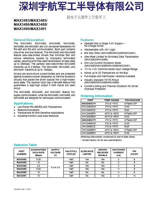
General Description The MAX3483, MAX3485, MAX3486, MAX3488,MAX3490, and MAX3491 are 3.3V , low-power transceivers forRS-485 and RS-422 communication. Each part containsone driver and one receiver. The MAX3483 and MAX3488feature slew-rate-limited drivers that minimize EMI andreduce reflections caused by improperly terminatedcables, allowing error-free data transmission at data ratesup to 250kbps. The partially slew-rate-limited MAX3486transmits up to 2.5Mbps. The MAX3485, MAX3490, andMAX3491 transmit at up to 10Mbps.Drivers are short-circuit current-limited and are protectedagainst excessive power dissipation by thermal shutdowncircuitry that places the driver outputs into a high-imped-ance state. The receiver input has a fail-safe feature thatguarantees a logic-high output if both inputs are opencircuit.The MAX3488, MAX3490, and MAX3491 feature full-duplex communication, while the MAX3483, MAX3485, andMAX3486 are designed for half-duplex communication.Applications ●Low-Power RS-485/RS-422 Transceivers ●Telecommunications ●Transceivers for EMI-Sensitive Applications ●Industrial-Control Local Area NetworksFeatures●Operate from a Single 3.3V Supply—No Charge Pump!●Interoperable with +5V Logic ●8ns Max Skew (MAX3485/MAX3490/MAX3491)●Slew-Rate Limited for Errorless Data Transmission (MAX3483/MAX3488)●2nA Low-Current Shutdown Mode (MAX3483/MAX3485/MAX3486/MAX3491)●-7V to +12V Common-Mode Input Voltage Range ●Allows up to 32 Transceivers on the Bus ●Full-Duplex and Half-Duplex Versions Available ●Industry Standard 75176 Pinout (MAX3483/MAX3485/MAX3486)●Current-Limiting and Thermal Shutdown for Driver Overload Protection 19-0333; Rev 1; 5/19Ordering Information continued at end of data sheet.*Contact factory for for dice specifications.PARTTEMP . RANGE PIN-PACKAGE MAX3483CPA0°C to +70°C 8 Plastic DIP MAX3483CSA0°C to +70°C 8 SO MAX3483C/D0°C to +70°C Dice*MAX3483EPA-40°C to +85°C 8 Plastic DIP MAX3483ESA-40°C to +85°C 8 SO MAX3485CPA0°C to +70°C 8 Plastic DIP MAX3485CSA0°C to +70°C 8 SO MAX3485C/D0°C to +70°C Dice*MAX3485EPA-40°C to +85°C 8 Plastic DIP MAX3485ESA -40°C to +85°C 8 SO PARTNUMBERGUARANTEED DATA RATE (Mbps)SUPPLY VOLTAGE (V)HALF/FULL DUPLEX SLEW-RATE LIMITED DRIVER/RECEIVER ENABLE SHUTDOWN CURRENT (nA)PIN COUNT MAX34830.25 3.0 to 3.6Half Yes Yes 28MAX348510Half No No 28MAX34862.5Half Yes Yes 28MAX34880.25Half Yes Yes —8MAX349010Half No No —8MAX349110Half No Yes 214MAX3483/MAX3485/MAX3486/MAX3488/MAX3490/MAX3491Selection TableOrdering Information找电子元器件上宇航军工Figure 1. MAX3483/MAX3485/MAX3486 Pin Configuration and Typical Operating Circuit Figure 2. MAX3488/MAX3490 Pin Configuration and Typical Operating Circuit Figure 3. MAX3491 Pin Configuration and Typical Operating CircuitMAX3486/MAX3488/MAX3490/MAX3491True RS-485/RS-422 TransceiversFigure 22. MAX3488/MAX3490/MAX3491 Full-Duplex RS-485 NetworkFigure 23. Line Repeater for MAX3488/MAX3490/MAX3491MAX3486/MAX3488/MAX3490/MAX3491True RS-485/RS-422 Transceivers。
MAX31865:温度检测器解决方案
MAX31865:温度检测器解决方案关键字:MAX31865 ,温度检测器解决方案MAX31865是一款集成的的RTD数字转换器,单芯片解决方案,能替代多个分立元件来降低成本。
MAX31865提供简单而准确的测量温度,是在工业领域常用的测量值,因此非常适合用于测量和过程控制应用。
MAX31865是完全集成的RTD数字转换器,该单芯片方案可将系统成本降低50%,并可处理工业设计中常见的铂RTD (如Pt100或Pt1000)电阻数字转换问题。
该器件能够简便、准确地测量温度,是工业测量和过程控制的理想选择。
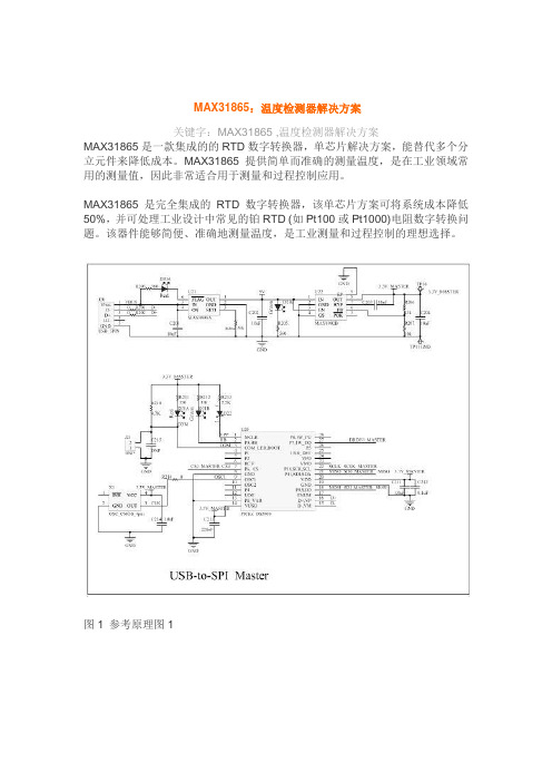
图1 参考原理图1图2 参考原理图2MAX31865主要特性•简单的数字值的转换铂RTD电阻•处理100Ω到1kΩ(0℃)PTRTD(PT100 PT1000)•适合于2、3和4线传感器连接•转换时间:最大21ms• 15位ADC分辨率;额定温度分辨率0.03125℃(由于RTD非线性变化) •在所有操作条件下的总精度:0.5℃(0.05%满量程)• ±50V的输入保护•全差分V REF输入•故障检测(开放式电阻元件、RTD输出范围电压、短路或短路电阻元件) • SPI兼容接口• 20引脚TQFN封装MAX31865方案特点MAX31865评估板(EV套件)提供了评估MAX31865 RTD,数字转换器的硬件和软件(图形用户界面)。
EV套件包括,一个MAX31865ATP,以及一个USB至SPI接口。
图3 toplayer 图图4 bottomlayer 图评估套件的USB至SPI主控部分可以用于与MAX31865评估板软件互动,并执行设备的功能。
•轻松评估MAX31865•完全组装和测试• USB HID接口•评估板硬件是USB供电(包括USB 电缆)AO-Electronics 傲壹电子官网: 中文网: • Windows XP,Windows Vista的和Windows7兼容软件•符合RoHS标准•验证的PCB布局。
MAX3225EAAP+中文资料

________________General DescriptionThe MAX3224E/MAX3225E/MAX3226E/MAX3227E/MAX3244E/MAX3245E are 3V-powered EIA/TIA-232and V.28/V.24 communications interfaces with automat-ic shutdown/wakeup features, high data-rate capabili-ties, and enhanced electrostatic discharge (ESD)protection. All transmitter outputs and receiver inputs are protected to ±15kV using IEC 1000-4-2 Air-Gap Discharge, ±8kV using IEC 1000-4-2 Contact Discharge,and ±15kV using the Human Body Model.All devices achieve a 1µA supply current using Maxim’s revolutionary AutoShutdown Plus™ feature. These devices automatically enter a low-power shutdown mode when the RS-232 cable is disconnected or the transmitters of the connected peripherals are inactive,and the UART driving the transmitter inputs is inactive for more than 30 seconds. They turn on again when they sense a valid transition at any transmitter or receiv-er input. AutoShutdown Plus saves power without changes to the existing BIOS or operating system.The MAX3225E/MAX3227E/MAX3245E also feature MegaBaud™ operation, guaranteeing 1Mbps for high-speed applications such as communicating with ISDN modems. The MAX3224E/MAX3226E/MAX3244E guar-antee 250kbps operation. The transceivers have a pro-prietary low-dropout transmitter output stage enabling true RS-232 performance from a +3.0V to +5.5V supply with a dual charge pump. The charge pump requires only four small 0.1µF capacitors for operation from a 3.3V supply. The MAX3224E–MAX3227E feature a logic-level output (READY) that asserts when the charge pump is regulating and the device is ready to begin transmitting.All devices are available in a space-saving TQFN,SSOP, and TSSOP (MAX3224E/MAX3225E/MAX3244E/MAX3245E) packages.________________________ApplicationsNotebook, Subnotebook, and Palmtop Computers Cellular PhonesBattery-Powered Equipment Hand-Held Equipment Peripherals Printers__Next Generation Device Features♦For Space-Constrained Applications:MAX3228E/MAX3229E: ±15kV ESD-Protected,+2.5V to +5.5V, RS-232 Transceivers in UCSP MAX3222E/MAX3232E/MAX3241E †/MAX3246E:±15kV ESD-Protected, Down to 10nA, +3.0V to +5.5V, Up to 1Mbps, True RS-232 Transceivers (MAX3246E Available in UCSP™)♦For Low-Voltage or Data Cable Applications:MAX3380E/MAX3381E: +2.35V to +5.5V, 1µA,2Tx/2Rx RS-232 Transceivers with ±15kV ESD-Protected I/O and Logic PinsMAX3224E–MAX3227E/MAX3244E/MAX3245E †±15kV ESD-Protected, 1µA, 1Mbps, 3.0V to 5.5V ,RS-232 Transceivers with AutoShutdown Plus________________________________________________________________Maxim Integrated Products119-1339; Rev 9; 2/07Ordering Information continued at end of data sheet.*EP = Exposed paddle.†Covered by U.S. Patent numbers 4,636,930; 4,679,134; 4,777,577;4,797,899; 4,809,152; 4,897,774; 4,999,761; 5,649,210; and other patents pending.AutoShutdown Plus, MegaBaud, and UCSP are trademarks of Maxim Integrated Products, Inc.Ordering InformationFor pricing, delivery, and ordering information,please contact Maxim/Dallas Direct!at 1-888-629-4642, or visit Maxim’s website at .M A X 3224E –M A X 3227E /M A X 3244E /M A X 3245E †±15kV ESD-Protected, 1µA, 1Mbps, 3.0V to 5.5V ,RS-232 Transceivers with AutoShutdown PlusABSOLUTE MAXIMUM RATINGSELECTRICAL CHARACTERISTICS(V CC = +3V to +5.5V, C1–C4 = 0.1µF, tested at 3.3V ±10%; C 1= 0.047µF, C2–C4 = 0.33µF, tested at 5.0V ±10%; T A = T MIN to T MAX ,unless otherwise noted. Typical values are at T A = +25°C.)Stresses beyond those listed under “Absolute Maximum Ratings” may cause permanent damage to the device. These are stress ratings only, and functional operation of the device at these or any other conditions beyond those indicated in the operational sections of the specifications is not implied. Exposure to absolute maximum rating conditions for extended periods may affect device reliability.V CC to GND..............................................................-0.3V to +6V V+ to GND (Note 1)..................................................-0.3V to +7V V- to GND (Note 1)...................................................+0.3V to -7V V+ +⏐V-⏐(Note 1)................................................................+13V Input Voltages T_IN, FORCEON, FORCEOFF to GND................-0.3V to +6V R_IN to GND....................................................................±25V Output Voltages T_OUT to GND.............................................................±13.2V R_OUT, INVALID , READY to GND.........-0.3V to (V CC + 0.3V)Short-Circuit Duration T_OUT to GND.......................................................Continuous Continuous Power Dissipation (T A = +70°C)16-Pin SSOP (derate 7.14mW/°C above +70°C).........571mW 16-Pin TSSOP (derate 9.4mW/°C above +70°C)......754.7mW 16-Pin TQFN (derate 20.8mW/°C above +70°C)....1666.7mW20-Pin TQFN (derate 21.3mW/°C above +70°C)....1702.1mW 20-Pin Plastic DIP (derate 11.11mW/°C above +70°C)...889mW 20-Pin SSOP (derate 8.00mW/°C above +70°C).........640mW 20-Pin TSSOP (derate 10.9mW/°C above +70°C).......879mW 28-Pin Wide SO (derate 12.5mW/°C above +70°C)............1W 28-Pin SSOP (derate 9.52mW/°C above +70°C).........762mW 28-Pin TSSOP (derate 12.8mW/°C above +70°C).......1026mW 36-Pin TQFN (derate 26.3mW/°C above +70°C)...........2105mW Operating Temperature Ranges MAX32_ _EC_ _.................................................0°C to +70°C MAX32_ _EE_ _................................................-40°C to +85°C MAX32_ _EAA_..............................................-40°C to +125°C Storage Temperature Range.............................-65°C to +160°C Lead Temperature (soldering, 10s).................................+300°C Note 1:V+ and V- can have maximum magnitudes of 7V, but their absolute difference cannot exceed 13V.MAX3224E–MAX3227E/MAX3244E/MAX3245E †±15kV ESD-Protected, 1µA, 1Mbps, 3.0V to 5.5V ,RS-232 Transceivers with AutoShutdown Plus_______________________________________________________________________________________3ELECTRICAL CHARACTERISTICS (continued)(V CC = +3V to +5.5V, C1–C4 = 0.1µF, tested at 3.3V ±10%; C 1= 0.047µF, C2–C4 = 0.33µF, tested at 5.0V ±10%; T A = T MIN to T MAX ,unless otherwise noted. Typical values are at T A = +25°C.)M A X 3224E –M A X 3227E /M A X 3244E /M A X 3245E †±15kV ESD-Protected, 1µA, 1Mbps, 3.0V to 5.5V ,RS-232 Transceivers with AutoShutdown Plus 4_______________________________________________________________________________________TIMING CHARACTERISTICS—MAX3224E/MAX3226E/MAX3244E(V CC = +3V to +5.5V, C1–C4 = 0.1µF, tested at 3.3V ±10%; C 1= 0.047µF, C2–C4 = 0.33µF, tested at 5.0V ±10%; T A = T MIN to T MAX ,unless otherwise noted. Typical values are at T A = +25°C.)TIMING CHARACTERISTICS—MAX3225E/MAX3227E/MAX3245E(V CC = +3V to +5.5V, C1–C4 = 0.1µF, tested at 3.3V ±10%; C 1= 0.047µF, C2–C4 = 0.33µF, tested at 5.0V ±10%; T A = T MIN to T MAX ,unless otherwise noted. Typical values are at T= +25°C.)Note 3:Transmitter skew is measured at the transmitter zero cross points.MAX3224E–MAX3227E/MAX3244E/MAX3245E †±15kV ESD-Protected, 1µA, 1Mbps, 3.0V to 5.5V ,RS-232 Transceivers with AutoShutdown Plus_______________________________________________________________________________________5-6-5-4-3-2-10123456010002000300040005000MAX3224E/MAX3226ETRANSMITTER OUTPUT VOLTAGEvs. LOAD CAPACITANCELOAD CAPACITANCE (pF)T R A N S M I T T E R O U T P U T V O L T A G E (V )246810121416010002000300040005000MAX3224E/MAX3226ESLEW RATE vs. LOAD CAPACITANCELOAD CAPACITANCE (pF)S L E W R A T E (V /μs )5101520253035404520001000300040005000MAX3224E/MAX3226E OPERATING SUPPLY CURRENT vs. LOAD CAPACITANCELOAD CAPACITANCE (pF)S U P P L Y C U R R E N T (m A )-7.50-2.5-5.02.55.07.501000500150020002500MAX3225E/MAX3227ETRANSMITTER OUTPUT VOLTAGEvs. LOAD CAPACITANCELOAD CAPACITANCE (pF)T R A N S M I T T E R O U T P U T V O L T A G E (V )1510520253035404550010005001500200025003000MAX3225E/MAX3227E TRANSMITTER SKEW vs. LOAD CAPACITANCELOAD CAPACITANCE (pF)T R A N S M I T T E R S K E W (n s)807060504030201005001000150020002500MAX3225E/MAX3227ESLEW RATE vs. LOAD CAPACITANCELOAD CAPACITANCE (pF)S L E W R A T E (V /μs )2010403060507090801005001000150020002500MAX3225E/MAX3227E OPERATING SUPPLY CURRENT vs. LOAD CAPACITANCELOAD CAPACITANCE (pF)S U P P L Y C U R R E N T (m A )20242230282636343238-40020-20406080100MAX3224E–MAX3227E READY TURN-ON TIME vs. TEMPERATURETEMPERATURE (°C)R E A D Y T U R N -O N T I M E (μs )__________________________________________Typical Operating Characteristics(V CC = +3.3V, 250kbps data rate, 0.1µF capacitors, all transmitters loaded with 3k Ωand C L , T A = +25°C, unless otherwise noted.)20018016014012010080604020-40020-20406080100MAX3224E–MAX3227E READY TURN-OFF TIME vs. TEMPERATUREM A X 3224-7/44/45E -09TEMPERATURE (°C)R E A D Y T U R N -O F F T I M E (n s )M A X 3224E –M A X 3227E /M A X 3244E /M A X 3245E †±15kV ESD-Protected, 1µA, 1Mbps, 3.0V to 5.5V ,RS-232 Transceivers with AutoShutdown Plus 6____________________________________________________________________________________________________________________Typical Operating Characteristics (continued)(V CC = +3.3V, 250kbps data rate, 0.1µF capacitors, all transmitters loaded with 3k Ωand C L , T A = +25°C, unless otherwise noted.)-6-5-4-3-2-10123456010002000300040005000MAX3244ETRANSMITTER OUTPUT VOLTAGEvs. LOAD CAPACITANCELOAD CAPACITANCE (pF)T R A N S M I T T E R O U T P U T V O L T A G E (V )4286121014010002000300040005000MAX3244ESLEW RATE vs. LOAD CAPACITANCEM A X 3224-7/44/45E -11LOAD CAPACITANCE (pF)S L E W R A T E (V /μs )302010405060020001000300040005000MAX3244EOPERATING SUPPLY CURRENT vs. LOAD CAPACITANCELOAD CAPACITANCE (pF)S U P P L Y C U R R E N T (m A )-7.50-2.5-5.02.55.07.50800400120016002000MAX3245ETRANSMITTER OUTPUT VOLTAGEvs. LOAD CAPACITANCELOAD CAPACITANCE (pF)T R A N S M I T T E R O U T P U T V O L T A G E (V )2010403060507090801000400800120016002000MAX3245EOPERATING SUPPLY CURRENT vs. LOAD CAPACITANCELOAD CAPACITANCE (pF)S U P P L Y C U R R E N T (m A )201040306050700400800120016002000MAX3245ESLEW RATE vs. LOAD CAPACITANCELOAD CAPACITANCE (pF)S L E W R A T E (V /μs )1510520253035404550100020003000MAX3245E TRANSMITT SKEW vs. LOAD CAPACITANCEM A X 3224-7/44/45E -16LOAD CAPACITANCE (pF)T R A N S M I T T E R S K E W (n s )MAX3224E–MAX3227E/MAX3244E/MAX3245E †±15kV ESD-Protected, 1µA, 1Mbps, 3.0V to 5.5V ,RS-232 Transceivers with AutoShutdown Plus_______________________________________________________________________________________7M A X 3224E –M A X 3227E /M A X 3244E /M A X 3245E †±15kV ESD-Protected, 1µA, 1Mbps 3.0V to 5.5V ,RS-232 Transceivers with AutoShutdown Plus 8_______________________________________________________________________________________Dual Charge-Pump Voltage ConverterThe MAX3224E–MAX3227E/MAX3244E/MAX3245E’s internal power supply consists of a regulated dual charge pump that provides output voltages of +5.5V (doubling charge pump) and -5.5V (inverting charge pump), over the +3.0V to +5.5V range. The charge pump operates in discontinuous mode: if the output voltages are less than 5.5V, the charge pump ischarge-pump is disabled. Each charge pump requires a flying capacitor (C1, C2) and a reservoir capacitor (C3, C4) to generate the V+ and V- supplies.The READY output (MAX3224E–MAX3227E) is low when the charge pumps are disabled in shutdown mode. The READY signal asserts high when V- goes below -4V.MAX3224E–MAX3227E/MAX3244E/MAX3245E †±15kV ESD-Protected, 1µA, 1Mbps 3.0V to 5.5V ,RS-232 Transceivers with AutoShutdown Plus_______________________________________________________________________________________9RS-232 TransmittersThe transmitters are inverting level translators that convert CMOS-logic levels to 5.0V EIA/TIA-232 levels.The MAX3224E/MAX3226E/MAX3244E guarantee a 250kbps data rate (1Mbps, for the MAX3225E/MAX3227E/MAX3245E) with worst-case loads of 3k Ωin parallel with 1000pF, providing compatibility with PC-to-PC com-munication software (such as LapLink™). Transmitters can be paralleled to drive multiple receivers. Figure 1shows a complete system connection.When FORCEOFF is driven to ground or when the Auto-Shutdown Plus circuitry senses that all receiver and transmitter inputs are inactive for more than 30s, the transmitters are disabled and the outputs go into a high-impedance state. When powered off or shut down, the outputs can be driven to ±12V. The transmitter inputs do not have pullup resistors. Connect unused inputs to GND or V CC .Figure 1. Interface Under Control of PMUFigure 2. The MAX3244E/MAX3245E detect RS-232 activity when the UART and interface are shut down.LapLink is a trademark of Traveling Software.M A X 3224E –M A X 3227E /M A X 3244E /M A X 3245E †±15kV ESD-Protected, 1µA, 1Mbps 3.0V to 5.5V ,RS-232 Transceivers with AutoShutdown Plus 10______________________________________________________________________________________RS-232 ReceiversThe receivers convert RS-232 signals to CMOS-logic output levels. The MAX3224E–MAX3227E feature inverting outputs that always remain active (Table 1).The MAX3244E/MAX3245E have inverting three-state outputs that are high impedance when shut down (FORCEOFF = GND) (Table 1).The MAX3244E/MAX3245E feature an extra, always active, noninverting output, R2OUTB. R2OUTB output monitors receiver activity while the other receivers are high impedance, allowing ring indicator applications to be monitored without forward biasing other devices connected to the receiver outputs. This is ideal for sys-tems where V CC is set to ground in shutdown to accommodate peripherals such as UARTs (Figure 2).The MAX3224E–MAX3227E/MAX3244E/MAX3245E fea-ture an INVALID output that is enabled low when no valid RS-232 voltage levels have been detected on all receiver inputs. Because INVALID indicates the receiv-er input’s condition, it is independent of FORCEON and FORCEOFF states (Figures 3 and 4).AutoShutdown Plus ModeThe MAX3224E–MAX3227E/MAX3244E/MAX3245E achieve a 1µA supplycurrent with Maxim’s AutoShutdown Plus feature, which operates when FORCEOFF is high and a FORCEON is low. When these devices do not sense a valid signal transition on any receiver and trans-mitter input for 30s, the on-board charge pumps are shut down, reducing supply current to 1µA. This occurs if the RS-232 cable is disconnected or if the connectedTable 1. Output Control Truth TableX = Don’t care*INVALID connected to FORCEON**INVALID connected to FORCEON and FORCEOFFMAX3224E–MAX3227E/MAX3244E/MAX3245E †±15kV ESD-Protected, 1µA, 1Mbps 3.0V to 5.5V ,RS-232 Transceivers with AutoShutdown Plusperipheral transmitters are turned off, and the UART dri-ving the transmitter inputs is inactive. The system turns on again when a valid transition is applied to any RS-232 receiver or transmitter input. As a result, the sys-tem saves power without changes to the existing BIOS or operating system.Figures 3a and 3b depict valid and invalid RS-232receiver voltage levels. INVALID indicates the receiver input’s condition, and is independent of FORCEON and FORCEOFF states. Figure 3 and Tables 1 and 2 sum-marize the operating modes of the MAX3224E–MAX3227E/MAX3244E/MAX3245E. FORCEON and FORCEOFF override AutoShutdown Plus circuitry.When neither control is asserted, the IC selects between these states automatically based on the last receiver or transmitter input edge received.When shut down, the device’s charge pumps turn off,V+ is pulled to V CC , V- is pulled to ground, the transmit-ter outputs are high impedance, and READY (MAX3224E–MAX3227E) is driven low. The time required to exit shutdown is typically 100µs (Figure 8).By connecting FORCEON to INVALID , the MAX3224E–MAX3227E/MAX3244E/MAX3245E shut down when no valid receiver level and no receiver or transmitter edge is detected for 30s, and wake up when a valid receiver level or receiver or transmitter edge is detected.Figure 3a. INVALID Functional Diagram, INVALID Low Figure 3b. INVALID Functional Diagram, INVALID HighFigure 3c. AutoShutdown Plus LogicFigure 3d. Power-Down LogicFigure 4a. Receiver Positive/Negative Thresholds for INVALIDM A X 3224E –M A X 3227E /M A X 3244E /M A X 3245E †±15kV ESD-Protected, 1µA, 1Mbps 3.0V to 5.5V ,RS-232 Transceivers with AutoShutdown PlusBy connecting FORCEON and FORCEOFF to INVALID ,the MAX3224E–MAX3227E/MAX3244E/MAX3245E shut down when no valid receiver level is detected and wake up when a valid receiver level is detected (same functionality as AutoShutdown feature on MAX3221E/MAX3223E/MAX3243E).A mouse or other system with AutoShutdown Plus may need time to wake up. Figure 5 shows a circuit that forces the transmitters on for 100ms, allowing enough time for the other system to realize that the MAX3244E/MAX3245E is awake. If the other system outputs valid RS-232 signal transitions within that time, the RS-232ports on both systems remain enabled.Software-Controlled ShutdownIf direct software control is desired, use INVALID to indicate DTR or ring indicator signal. Tie FORCEOFF and FORCEON together to bypass the AutoShutdown Plus so the line acts like a SHDN input.±15kV ESD ProtectionAs with all Maxim devices, ESD-protection structures are incorporated on all pins to protect against electrostaticdischarges encountered during handling and assembly.The driver outputs and receiver inputs of the MAX3224E–MAX3227E/MAX3244E/MAX3245E have extra protection against static electricity. Maxim’s engineers have developed state-of-the-art structures to protectFigure 4b. AutoShutdown Plus, INVALID,and READY Timing DiagramFigure 5. AutoShutdown Plus Initial Turn-On to Wake Up a Mouse or Another SystemMAX3224E–MAX3227E/MAX3244E/MAX3245E †±15kV ESD-Protected, 1µA, 1Mbps 3.0V to 5.5V ,RS-232 Transceivers with AutoShutdown Plusthese pins against ESD of ±15kV without damage. The ESD structures withstand high ESD in all states: normal operation, shutdown, and powered down. After an ESD event, Maxim’s E versions keep working without latchup, whereas competing RS-232 products can latch and must be powered down to remove latchup.ESD protection can be tested in various ways; the transmitter outputs and receiver inputs of this product family are characterized for protection to the following limits:1)±15kV using the Human Body Model2)±8kV using the Contact-Discharge Method specified in IEC1000-4-23)±15kV using IEC1000-4-2’s Air-Gap Method.ESD Test ConditionsESD performance depends on a variety of conditions.Contact Maxim for a reliability report that documents test setup, test methodology, and test results.Human Body ModelFigure 6a shows the Human Body Model and Figure 6b shows the current waveform it generates when dis-charged into a low impedance. This model consists of a 100pF capacitor charged to the ESD voltage of inter-est, which is then discharged into the test device through a 1.5k Ωresistor.Figure 6b. Human Body Current WaveformFigure 7b. IEC1000-4-2 ESD Generator Current WaveformFigure 6a. Human Body ESD Test Model Figure 7a. IEC1000-4-2 ESD Test ModelM A X 3224E –M A X 3227E /M A X 3244E /M A X 3245E †±15kV ESD-Protected, 1µA, 1Mbps 3.0V to 5.5V ,RS-232 Transceivers with AutoShutdown Plus IEC1000-4-2The IEC1000-4-2 standard covers ESD testing and per-formance of finished equipment; it does not specifically refer to integrated circuits. The MAX3224E–MAX3227E,MAX3244E/MAX3245E help you design equipment that meets Level 4 (the highest level) of IEC1000-4-2, with-out the need for additional ESD-protection components.The major difference between tests done using the H uman Body Model and IEC1000-4-2 is higher peak current in IEC1000-4-2, because series resistance is lower in the IEC1000-4-2 model. Hence, the ESD with-stand voltage measured to IEC1000-4-2 is generally lower than that measured using the H uman Body Model. Figure 7a shows the IEC1000-4-2 model and Figure 7b shows the current waveform for the 8kV,IEC1000-4-2, Level 4, ESD Contact-Discharge Method.The Air-Gap Method involves approaching the device with a charged probe. The Contact-Discharge Method connects the probe to the device before the probe is energized.Machine ModelThe Machine Model for ESD tests all pins using a 200pF storage capacitor and zero discharge resis-tance. Its objective is to emulate the stress caused by contact that occurs with handling and assembly during manufacturing. Of course, all pins require this protec-tion during manufacturing, not just RS-232 inputs and outputs. Therefore, after PC board assembly, the Machine Model is less relevant to I/O ports.__________Applications InformationCapacitor SelectionThe capacitor type used for C1–C4 is not critical for proper operation; polarized or nonpolarized capacitorscan be used. The charge pump requires 0.1µF capaci-tors for 3.3V operation. For other supply voltages, see Table 3 for required capacitor values. Do not use val-ues smaller than those listed in Table 3. Increasing the capacitor values (e.g., by a factor of 2) reduces ripple on the transmitter outputs and slightly reduces power consumption. C2, C3, and C4 can be increased without changing C1’s value. However, do not increase C1without also increasing the values of C2, C3, C4,and C BYPASS , to maintain the proper ratios (C1 to the other capacitors).When using the minimum required capacitor values,make sure the capacitor value does not degrade excessively with temperature. If in doubt, use capaci-tors with a larger nominal value. The capacitor’s equiv-alent series resistance (ESR), which usually rises at low temperatures, influences the amount of ripple on V+and V-.Power-Supply DecouplingIn most circumstances, a 0.1µF V CC bypass capacitor is adequate. In applications that are sensitive to power-supply noise, use a capacitor of the same value as charge-pump capacitor C1. Connect bypass capaci-tors as close to the IC as possible.Transmitter Outputs when Exiting ShutdownFigure 8 shows two transmitter outputs when exiting shutdown mode. As they become active, the two trans-mitter outputs are shown going to opposite RS-232 lev-els (one transmitter input is high, the other is low). Each5μs/divV CC = 3.3V C1–C4 = 0.1μFFigure 8. Transmitter Outputs when Exiting Shutdown or Powering Uptransmitter is loaded with 3k Ωin parallel with 1000pF.The transmitter outputs display no ringing or undesir-able transients as they come out of shutdown. Note that the transmitters are enabled only when the magnitude of V- exceeds approximately -3V.High Data RatesThe MAX3224E/MAX3226E/MAX3244E maintain the RS-232 ±5.0V minimum transmitter output voltage even at high data rates. Figure 9 shows a transmitter loop-back test circuit. Figure 10 shows a loopback test result at 120kbps, and Figure 11 shows the same test at 250kbps. For Figure 10, all transmitters were driven simultaneously at 120kbps into RS-232 loads in parallel with 1000pF. For Figure 11, a single transmitter was dri-ven at 250kbps, and all transmitters were loaded with an RS-232 receiver in parallel with 250pF.The MAX3225E/MAX3227E/MAX3245E maintain the RS-232 ±5.0V minimum transmitter output voltage at data rates up to 1Mbps (MegaBaud). Figure 12 shows a loopback test result with a single transmitter driven at 1Mbps and all transmitters loaded with an RS-232receiver in parallel with 250pF.MAX3224E–MAX3227E/MAX3244E/MAX3245E †±15kV ESD-Protected, 1µA, 1Mbps 3.0V to 5.5V ,RS-232 Transceivers with AutoShutdown PlusFigure 9. Loopback Test CircuitFigure 10. MAX3224E/MAX3226E/MAX3244E Loopback Test Result at 120kbps2μs/divV CC = 3.3VFigure 11. MAX3224E/MAX3226E/MAX3244E Loopback Test Result at 250kbps2μs/divV CC = 3.3VFigure 12. MAX3225E/MAX3227E/MAX3245E Loopback Test Result at 1Mbps200ns/div5V/div5V/div5V/divV CC = 3.3VM A X 3224E –M A X 3227E /M A X 3244E /M A X 3245E †±15kV ESD-Protected, 1µA, 1Mbps 3.0V to 5.5V ,RS-232 Transceivers with AutoShutdown Plus Figure 13a. Mouse Driver Test CircuitMAX3224E–MAX3227E/MAX3244E/MAX3245E †±15kV ESD-Protected, 1µA, 1Mbps 3.0V to 5.5V ,RS-232 Transceivers with AutoShutdown PlusMouse DriveabilityThe MAX3244E/MAX3245E are specifically designed to power serial mice while operating from low-voltage power supplies. They have been tested with leading mouse brands from manufacturers such as Microsoft and Logitech. The MAX3244E/MAX3245E successfully drove all serial mice tested and met their respective current and voltage requirements. The MAX3244E/MAX3245E dual charge pump ensures the transmitters supply at least ±5V during worst-case conditions.Figure 13b shows the transmitter output voltages under increasing load current. Figure 13a shows a typical mouse connection.Interconnection with 3V and 5V LogicThe MAX3224E–MAX3227E/MAX3244E/MAX3245E can directly interface with various 5V logic families, includ-ing ACT and HCT CMOS. See Table 4 for more informa-tion on possible combinations of interconnections.Table 5 lists other Maxim ESD-powered transceivers.Table 5. ±15kV ESD-Protected, 3.0V to 5.5V Powered RS-232 Transceivers from MaximM A X 3224E –M A X 3227E /M A X 3244E /M A X 3245E †±15kV ESD-Protected, 1µA, 1Mbps 3.0V to 5.5V ,RS-232 Transceivers with AutoShutdown Plus___________________________________________________Typical Operating CircuitsMAX3224E–MAX3227E/MAX3244E/MAX3245E †±15kV ESD-Protected, 1µA, 1Mbps 3.0V to 5.5V ,RS-232 Transceivers with AutoShutdown Plus___________________________________________________________Pin ConfigurationsM A X 3224E –M A X 3227E /M A X 3244E /M A X 3245E †±15kV ESD-Protected, 1µA, 1Mbps 3.0V to 5.5V ,RS-232 Transceivers with AutoShutdown Plus ___________________________________________Ordering Information (continued)___________________Chip InformationMAX3224E TRANSISTOR COUNT: 1129MAX3225E TRANSISTOR COUNT: 1129MAX3226E TRANSISTOR COUNT: 1129MAX3227E TRANSISTOR COUNT: 1129MAX3244E/MAX3245E TRANSISTOR COUNT: 1335PROCESS: BICMOS*EP = Exposed paddle.MAX3224E–MAX3227E/MAX3244E/MAX3245E †±15kV ESD-Protected, 1µA, 1Mbps 3.0V to 5.5V ,RS-232 Transceivers with AutoShutdown Plus______________________________________________________________________________________21Package Information(The package drawing(s) in this data sheet may not reflect the most current specifications. For the latest package outline information,go to /packages .)。
MAX6305中文资料
For free samples & the latest literature: , or phone 1-800-998-8800.For small orders, phone 408-737-7600 ext. 3468.General DescriptionThe MAX6305–MAX6313 CMOS microprocessor (µP)supervisory circuits are designed to monitor more than one power supply. Ideal for monitoring both 5V and 3.3V in personal computer systems, these devicesFeatureso Small 5-Pin SOT23 Packageo Precision Factory-Set V CC Reset Thresholds;Available in 0.1V Increments from 2.5V to 5V o Immune to Short V TransientsMAX6305–MAX63135-Pin, Multiple-Input,Programmable Reset ICs________________________________________________________________Maxim Integrated Products 119-1145; Rev 1; 8/98M A X 6305–M A X 63135-Pin, Multiple-Input, Programmable Reset ICs 2_______________________________________________________________________________________ABSOLUTE MAXIMUM RATINGSELECTRICAL CHARACTERISTICSV CC = +2.5V to +5.5V for the MAX6305/MAX6308/MAX6311, V CC = (V TH + 2.5%) to +5.5V for the MAX6306/MAX6307/MAX6309/MAX6310/MAX6312/MAX6313; T A = 0°C to +70°C; unless otherwise noted. Typical values are at T A = +25°C.)Stresses beyond those listed under “Absolute Maximum Ratings” may cause permanent damage to the device. These are stress ratings only, and functional operation of the device at these or any other conditions beyond those indicated in the operational sections of the specifications is not implied. Exposure to absolute maximum rating conditions for extended periods may affect device reliability.V CC ...........................................................................-0.3V to +6V All Other Pins..............................................-0.3V to (V CC + 0.3V)Input/Output Current, All Pins.............................................20mA Rate of Rise, V CC ............................................................100V/µsContinuous Power Dissipation (T A = +70°C)SOT23-5 (derate 7.1mW/°C above +70°C).................571mW Operating Temperature Range...............................0°C to +70°C Storage Temperature Range.............................-65°C to +160°C Lead Temperature (soldering, 10sec).............................+300°CMAX6305–MAX63135-Pin, Multiple-Input, Programmable Reset ICs_______________________________________________________________________________________3ELECTRICAL CHARACTERISTICS (continued)(V CC = +2.5V to +5.5V for the MAX6305/MAX6308/MAX6311, V CC = (V TH + 2.5%) to +5.5V for the MAX6306/MAX6307/MAX6309/MAX6310/MAX6312/MAX6313; T A = 0°C to +70°C; unless otherwise noted. Typical values are at T A = +25°C.)Note 1: The MAX6305/MAX6308/MAX6311 switch from undervoltage reset to normal operation between 1.5V < V CC < 2.5V.Note 2: The MAX6306/MAX6307/MAX6309/MAX6310/MAX6312/MAX6313 monitor V CC through an internal factory-trimmed voltagedivider, which programs the nominal reset threshold. Factory-trimmed reset thresholds are available in approximately 100mV increments from 2.5V to 5V (Table 1).M A X 6305–M A X 63135-Pin, Multiple-Input, Programmable Reset ICs 4_________________________________________________________________________________________________________________________________Typical Operating Characteristics(V CC = +5V, T A = +25°C, unless otherwise noted.)5.05.56.06.57.07.58.08.59.09.5-60-40-2020406080100SUPPLY CURRENT vs. TEMPERATURETEMPERATURE (°C)S U P P L Y C U R R E N T (µA )01020304050607080-60-40-2020406080100V CC FALLING PROPAGATION DELAYvs. TEMPERATURETEMPERATURE (°C)P R O P A G A T I O N D E L A Y (n s )010203040506070-60-40-20020406080100OVRST IN RISING PROPAGATION DELAY vs. TEMPERATURE (OVERVOLTAGE RESET INPUT)TEMPERATURE (°C)P R O P A G A T I O N D E L A Y (n s )020406080100120-60-40-2020406080100RST IN_ FALLING PROPAGATION DELAY vs. TEMPERATURETEMPERATURE (°C)R S T I N _ P R O P A G A T I O N D E L A Y (n s )104001200800MAXIMUM TRANSIENT DURATION vs.V CC RESET THRESHOLD OVERDRIVE10OVERDRIVE, V TH - V CC (mV)T R A N S I E N T D U R A T I O N (µs )100100010,0000.900.920.940.960.981.001.021.041.061.081.10-60-40-20020406080100RESET TIMEOUT vs. TEMPERATURE6305 T O C 05TEMPERATURE (°C)N O R M A L I Z E D R E S E T T I M E O U T0.9900.9920.9940.9960.9981.0001.0021.0041.0061.0081.010-60-40-2020406080100RESET THRESHOLD vs. TEMPERATURE6305 T O C 06TEMPERATURE (°C)N O R M A L I Z E D R E S E T T H R E S H O L D (V /V )104001200800MAXIMUM TRANSIENT DURATION vs.OVRST IN THRESHOLD OVERDRIVE10OVERDRIVE, V OVRST IN - V REF (mV)T R A N S I E N T D U R A T I O N (µs )100100010,000104001200800MAXIMUM TRANSIENT DURATION vs.RST IN_ THRESHOLD OVERDRIVE10OVERDRIVE, V REF - V RST IN (mV)T R A N S I E N T D U R A T I O N (µs )100100010,000_______________Detailed DescriptionThe MAX6305–MAX6313 CMOS microprocessor (µP)supervisory circuits are designed to monitor more than one power supply and issue a system reset when any monitored supply falls out of regulation. The MAX6305/MAX6308/MAX6311 have two adjustable undervoltage reset inputs (RST IN1 and RST IN2). The MAX6306/MAX6307/MAX6309/MAX6310/MAX6312/MAX6313 mon-itor V CC through an internal, factory-trimmed voltage divider. The MAX6306/MAX6309/MAX6312 have, in addition, an adjustable undervoltage reset input and a manual-reset input. The internal voltage divider sets the reset threshold as specified in the device part number (Table 1). The MAX6307/MAX6310/ MAX6313 feature an adjustable undervoltage reset input (RST IN) and an adjustable overvoltage reset input (OVRST IN) in addition to the factory-trimmed reset threshold on the V CC moni-tor. Program the adjustable reset inputs with an external resistor divider (see Adjustable Reset Inputs section).Reset OutputsA µP’s reset input starts the µP in a known state. These µP supervisory circuits assert reset to prevent code-execution errors during power-up, power-down, or brownout conditions.RESET (MAX6305–MAX6310) and RESET (MAX6311/MAX6312/MAX6313) are guaranteed to be asserted at a valid logic level for V CC > 1V (see Electrical Characteristics ). Once all monitored voltages exceed their programmed reset thresholds, an internal timer keeps reset asserted for the reset timeout period (t RP );after this interval, reset deasserts.If a brownout condition occurs (any or all monitored volt-ages dip outside their programmed reset threshold),reset asserts (RESET goes high; RESET goes low). Any time any of the monitored voltages dip below their reset threshold, the internal timer resets to zero and reset asserts. The internal timer starts when all of the moni-tored voltages return above their reset thresholds, and reset remains asserted for a reset timeout period. The MAX6305/MAX6306/MAX6307 feature an active-low,MAX6305–MAX63135-Pin, Multiple-Input, Programmable Reset ICs_______________________________________________________________________________________5______________________________________________________________Pin DescriptionM A X 6305–M A X 6313open-drain, N-channel output. The MAX6308/MAX6309/MAX6310 feature an active-low, complementary output structure that both sinks and sources current, and the MAX6311/MAX6312/MAX6313 have an active-high com-plementary reset output.The MAX6305/MAX6308/MAX6311 switch from under-voltage lockout operation to normal operation between 1.5V < V CC < 2.5V. Below 1.5V, V CC undervoltage-lockout mode asserts RESET . Above 2.5V, V CC normal-operation mode asserts reset if RST IN_ falls below the RST IN_ threshold.Manual-Reset Input(MAX6306/MAX6309/MAX6312)Many µP-based products require manual-reset capability,allowing an operator or external logic circuitry to initiate a reset. A logic low on MR asserts reset. Reset remains asserted while MR is low, and for a reset active timeout period (t RP ) after MR returns high. This input has an inter-nal 63.5k Ωpull-up resistor, so it can be left open if it is not used. MR can be driven with TTL-logic levels in 5V sys-tems, with CMOS-logic levels in 3V systems, or with open-drain/collector output devices. Connect a normally open momentary switch from MR to GND to create a manual-reset function; external debounce circuitry is not required.If MR is driven from long cables or if the device is used in a noisy environment, connecting a 0.1µF capacitor from MR to ground provides additional noise immunity.The MR pin has internal ESD-protection circuitry that may be forward biased under certain conditions, drawing excessive current. For example, assume the circuitry driv-ing MR uses a +5V supply other than V CC . If V CC drops or browns out lower than +4.7V, MR ’s absolute maximum rat-ing is violated (-0.3V to (V CC + 0.3V)), and undesirable current flows through the ESD structure from MR to V CC .To avoid this, it is recommended that the supply for the MR pin be the same as the supply monitored by V CC . In this way, the voltage at MR will not exceed V CC .Adjustable Reset InputsThe MAX6305–MAX6313 each have one or more reset inputs (RST IN_ /OVRST IN). These inputs are com-pared to the internal reference voltage (Figure 1).Connect a resistor voltage divider to RST IN_ such that V RST IN_falls below V RSTH (1.23V) when the monitored voltage (V IN ) falls below the desired reset threshold (V TH ) (Figure 2). Calculate the desired reset voltage with the following formula:R1 + R2V TH = ________x V RSTHR25-Pin, Multiple-Input, Programmable Reset ICs 6_______________________________________________________________________________________Figure 1. Functional DiagramMAX6305–MAX63135-Pin, Multiple-Input, Programmable Reset ICs_______________________________________________________________________________________7The ±25nA max input leakage current allows resistors on the order of megohms. Choose the pull-up resistor in the divider to minimize the error due to the input leakage cur-rent. The error term in the calculated threshold is simply:±25nA x R1If you choose R1 to be 1M Ω, the resulting error is ±25 x 10-9x 1 x 106= ±25mV.Like the V CC voltage monitors on the MAX6306/MAX6307/MAX6309/MAX6310/MAX6312/MAX6313, the RST IN_inputs (when used with a voltage divider) are designed to ignore fast voltage transients. Increase the noise immunity by connecting a capacitor on the order of 0.1µF between RST IN and GND (Figure 2). This creates a single-pole lowpass filter with a corner frequency given by:f = (1/2π) / (R1 + R2)(R1 x R2 x C)For example, if R1 = 1M Ωand R2 = 1.6M Ω, adding a 0.1µF capacitor from RST IN_ to ground results in a lowpass corner frequency of f = 2.59Hz. Note that adding capacitance to RST IN slows the circuit’s overall response time.__________Applications InformationInterfacing to µPs with Bidirectional Reset PinsSince the RESET output on the MAX6305/MAX6306/MAX6307 is open drain, these devices interface easily with µPs that have bidirectional reset pins, such as the Motorola 68HC11. Connecting the µP supervisor’s RESET output directly to the microcontroller’s RESET pin with a single pull-up resistor allows either device to assert reset (Figure 3).Negative-Going V CC TransientsIn addition to issuing a reset to the µP during power-up,power-down, and brownout conditions, these devices are relatively immune to short-duration, negative-going V CC transients (glitches).The Typical Operating Characteristics show the Maximum Transient Duration vs. V CC Reset Threshold Overdrive, for which reset pulses are not generated.The graph was produced using negative-going pulses,starting at V TH max, and ending below the pro-grammed reset threshold by the magnitude indicated (reset threshold overdrive). The graph shows the maxi-mum pulse width that a negative-going V CC transient may typically have without causing a reset pulse to be issued. As the amplitude of the transient increases (i.e.,goes farther below the reset threshold), the maximum allowable pulse width decreases.RST IN_/OVRST IN are also immune to negative/positive-going transients (see Typical Operating Characteristics ).A 0.1µF bypass capacitor mounted close to the RST IN_,OVRST IN, and/or the V CC pin provides additional tran-sient immunity.Ensuring a Valid RESET /RESETOutput Down to V CC = 0VWhen V CC falls below 1V, push/pull structured RESET /RESET current sinking (or sourcing) capabilities decrease drastically. High-impedance CMOS-logic inputs connected to RESET can drift to undetermined voltages. This presents no problem in most applica-tions, since most µPs and other circuitry do not operate with V CC below 1V. In those applications where RESET must be valid down to 0V, adding a pull-down resistor between RESET and ground sinks any stray leakageFigure 2. Increasing Noise ImmunityFigure 3. Interfacing to µPs with Bidirectional Reset I/Ocurrents, holding RESET low (Figure 4). The pull-down resistor’s value is not critical; 100k Ωis large enough not to load RESET and small enough to pull RESET to ground. For applications where RESET must be valid to V CC , a 100k Ωpull-up resistor between RESET and V CC will hold RESET high when V CC falls below 1V (Figure 5).Since the MAX6305/MAX6306/MAX6307 have open-drain, active-low outputs, they typically use a pull-up resistor. With these devices and under these conditions (V CC < 1V), RESET will most likely not maintain an active condition, but will drift toward a nonactive level due to the pull-up resistor and the RESET output’s reduction in sinking capability. These devices are not recommended for applications that require a valid RESET output below 1V.* Factory-trimmed reset thresholds are available in approximately 100mV increments with a ±1.5% room-temperature variance.M A X 6305–M A X 63135-Pin, Multiple-Input, Programmable Reset ICs 8_______________________________________________________________________________________Figure 4. Ensuring RESET Valid to V CC = 0VFigure 5. Ensuring RESET Valid to V CC = 0VTable 1. Factory-Trimmed Reset Thresholds *MAX6305UK00D1-T ABAK MAX6306UK41D3-T ABCA MAX6306UK30D1-T ABDQ MAX6307UK46D3-T ABFG MAX6305UK00D2-T ABAL MAX6306UK41D4-T ABCB MAX6306UK30D2-T ABDR MAX6307UK46D4-T ABFH MAX6305UK00D3-T ABAM MAX6306UK40D1-T ABCC MAX6306UK30D3-T ABDS MAX6307UK45D1-T ABFI MAX6305UK00D4-T ABAN MAX6306UK40D2-T ABCD MAX6306UK30D4-T ABDT MAX6307UK45D2-T ABFJ MAX6306UK50D1-T ABAO MAX6306UK40D3-T ABCE MAX6306UK29D1-T ABDU MAX6307UK45D3-T ABFK MAX6306UK50D2-T ABAP MAX6306UK40D4-T ABCF MAX6306UK29D2-T ABDV MAX6307UK45D4-T ABFL MAX6306UK50D3-T ABAQ MAX6306UK39D1-T ABCG MAX6306UK29D3-T ABDW MAX6307UK44D1-T ABFM MAX6306UK50D4-T ABAR MAX6306UK39D2-T ABCH MAX6306UK29D4-T ABDX MAX6307UK44D2-T ABFN MAX6306UK49D1-T ABAS MAX6306UK39D3-T ABCI MAX6306UK28D1-T ABDY MAX6307UK44D3-T ABFO MAX6306UK49D2-T ABAT MAX6306UK39D4-T ABCJ MAX6306UK28D2-T ABDZ MAX6307UK44D4-T ABFP MAX6306UK49D3-T ABAU MAX6306UK38D1-T ABCK MAX6306UK28D3-T ABEA MAX6307UK43D1-T ABFQ MAX6306UK49D4-T ABAV MAX6306UK38D2-T ABCL MAX6306UK28D4-T ABEB MAX6307UK43D2-T ABFR MAX6306UK48D1-T ABAW MAX6306UK38D3-T ABCM MAX6306UK27D1-T ABEC MAX6307UK43D3-T ABFS MAX6306UK48D2-T ABAX MAX6306UK38D4-T ABCN MAX6306UK27D2-T ABED MAX6307UK43D4-T ABFT MAX6306UK48D3-T ABAY MAX6306UK37D1-T ABCO MAX6306UK27D3-T ABEE MAX6307UK42D1-T ABFU MAX6306UK48D4-T ABAZ MAX6306UK37D2-T ABCP MAX6306UK27D4-T ABEF MAX6307UK42D2-T ABFV MAX6306UK47D1-T ABBA MAX6306UK37D3-T ABCQ MAX6306UK26D1-T ABEG MAX6307UK42D3-T ABFW MAX6306UK47D2-T ABBB MAX6306UK37D4-T ABCR MAX6306UK26D2-T ABEH MAX6307UK42D4-T ABFX MAX6306UK47D3-T ABBC MAX6306UK36D1-T ABCS MAX6306UK26D3-T ABEI MAX6307UK41D1-T ABFY MAX6306UK47D4-T ABBD MAX6306UK36D2-T ABCT MAX6306UK26D4-T ABEJ MAX6307UK41D2-T ABFZ MAX6306UK46D1-T ABBE MAX6306UK36D3-T ABCU MAX6306UK25D1-T ABEK MAX6307UK41D3-T ABGA MAX6306UK46D2-T ABBF MAX6306UK36D4-T ABCV MAX6306UK25D2-T ABEL MAX6307UK41D4-T ABGB MAX6306UK46D3-T ABBG MAX6306UK35D1-T ABCW MAX6306UK25D3-T ABEM MAX6307UK40D1-T ABGC MAX6306UK46D4-T ABBH MAX6306UK35D2-T ABCX MAX6306UK25D4-T ABEN MAX6307UK40D2-T ABGD MAX6306UK45D1-T ABBI MAX6306UK35D3-T ABCY MAX6307UK50D1-T ABEO MAX6307UK40D3-T ABGE MAX6306UK45D2-T ABBJ MAX6306UK35D4-T ABCZ MAX6307UK50D2-T ABEP MAX6307UK40D4-T ABGF MAX6306UK45D3-T ABBK MAX6306UK34D1-T ABDA MAX6307UK50D3-T ABEQ MAX6307UK39D1-T ABGG MAX6306UK45D4-T ABBL MAX6306UK34D2-T ABDB MAX6307UK50D4-T ABER MAX6307UK39D2-T ABGH MAX6306UK44D1-T ABBM MAX6306UK34D3-T ABDC MAX6307UK49D1-T ABES MAX6307UK39D3-T ABGI MAX6306UK44D2-T ABBN MAX6306UK34D4-T ABDD MAX6307UK49D2-T ABET MAX6307UK39D4-T ABGJ MAX6306UK44D3-T ABBO MAX6306UK33D1-T ABDE MAX6307UK49D3-T ABEU MAX6307UK38D1-T ABGK MAX6306UK44D4-T ABBP MAX6306UK33D2-T ABDF MAX6307UK49D4-T ABEV MAX6307UK38D2-T ABGL MAX6306UK43D1-T ABBQ MAX6306UK33D3-T ABDG MAX6307UK48D1-T ABEW MAX6307UK38D3-T ABGM MAX6306UK43D2-T ABBR MAX6306UK33D4-T ABDH MAX6307UK48D2-T ABEX MAX6307UK38D4-T ABGN MAX6306UK43D3-T ABBS MAX6306UK32D1-T ABDI MAX6307UK48D3-T ABEY MAX6307UK37D1-T ABGO MAX6306UK43D4-T ABBT MAX6306UK32D2-T ABDJ MAX6307UK48D4-T ABEZ MAX6307UK37D2-T ABGP MAX6306UK42D1-T ABBU MAX6306UK32D3-T ABDK MAX6307UK47D1-T ABFA MAX6307UK37D3-T ABGQ MAX6306UK42D2-T ABBV MAX6306UK32D4-T ABDL MAX6307UK47D2-T ABFB MAX6307UK37D4-T ABGR MAX6306UK42D3-T ABBW MAX6306UK31D1-T ABDM MAX6307UK47D3-T ABFC MAX6307UK36D1-T ABGS MAX6306UK42D4-T ABBX MAX6306UK31D2-T ABDN MAX6307UK47D4-T ABFD MAX6307UK36D2-T ABGT MAX6306UK41D1-T ABBY MAX6306UK31D3-T ABDO MAX6307UK46D1-T ABFE MAX6307UK36D3-T ABGU MAX6306UK41D2-TABBZMAX6306UK31D4-TABDPMAX6307UK46D2-TABFFMAX6307UK36D4-TABGVMAX6305–MAX63135-Pin, Multiple-Input, Programmable Reset ICs_______________________________________________________________________________________9Table 2. Device Marking CodesDEVICECODE DEVICECODE DEVICECODE DEVICECODEM A X 6305–M A X 63135-Pin, Multiple-Input, Programmable Reset ICs 10______________________________________________________________________________________Table 2. Device Marking Codes (continued)MAX6307UK35D1-T ABGW MAX6307UK25D3-T ABIM MAX6309UK41D1-T ABKC MAX6309UK31D3-T ABLS MAX6307UK35D2-T ABGX MAX6307UK25D4-T ABIN MAX6309UK41D2-T ABKD MAX6309UK31D4-T ABLT MAX6307UK35D3-T ABGY MAX6308UK00D1-T ABIO MAX6309UK41D3-T ABKE MAX6309UK30D1-T ABLU MAX6307UK35D4-T ABGZ MAX6308UK00D2-T ABIP MAX6309UK41D4-T ABKF MAX6309UK30D2-T ABLV MAX6307UK34D1-T ABHA MAX6308UK00D3-T ABIQ MAX6309UK40D1-T ABKG MAX6309UK30D3-T ABLW MAX6307UK34D2-T ABHB MAX6308UK00D4-T ABIR MAX6309UK40D2-T ABKH MAX6309UK30D4-T ABLX MAX6307UK34D3-T ABHC MAX6309UK50D1-T ABIS MAX6309UK40D3-T ABKI MAX6309UK29D1-T ABLY MAX6307UK34D4-T ABHD MAX6309UK50D2-T ABIT MAX6309UK40D4-T ABKJ MAX6309UK29D2-T ABLZ MAX6307UK33D1-T ABHE MAX6309UK50D3-T ABIU MAX6309UK39D1-T ABKK MAX6309UK29D3-T ABMA MAX6307UK33D2-T ABHF MAX6309UK50D4-T ABIV MAX6309UK39D2-T ABKL MAX6309UK29D4-T ABMB MAX6307UK33D3-T ABHG MAX6309UK49D1-T ABIW MAX6309UK39D3-T ABKM MAX6309UK28D1-T ABMC MAX6307UK33D4-T ABHH MAX6309UK49D2-T ABIX MAX6309UK39D4-T ABKN MAX6309UK28D2-T ABMD MAX6307UK32D1-T ABHI MAX6309UK49D3-T ABIY MAX6309UK38D1-T ABKO MAX6309UK28D3-T ABME MAX6307UK32D2-T ABHJ MAX6309UK49D4-T ABIZ MAX6309UK38D2-T ABKP MAX6309UK28D4-T ABMF MAX6307UK32D3-T ABHK MAX6309UK48D1-T ABJA MAX6309UK38D3-T ABKQ MAX6309UK27D1-T ABMG MAX6307UK32D4-T ABHL MAX6309UK48D2-T ABJB MAX6309UK38D4-T ABKR MAX6309UK27D2-T ABMH MAX6307UK31D1-T ABHM MAX6309UK48D3-T ABJC MAX6309UK37D1-T ABKS MAX6309UK27D3-T ABMI MAX6307UK31D2-T ABHN MAX6309UK48D4-T ABJD MAX6309UK37D2-T ABKT MAX6309UK27D4-T ABMJ MAX6307UK31D3-T ABHO MAX6309UK47D1-T ABJE MAX6309UK37D3-T ABKU MAX6309UK26D1-T ABMK MAX6307UK31D4-T ABHP MAX6309UK47D2-T ABJF MAX6309UK37D4-T ABKV MAX6309UK26D2-T ABML MAX6307UK30D1-T ABHQ MAX6309UK47D3-T ABJG MAX6309UK36D1-T ABKW MAX6309UK26D3-T ABMM MAX6307UK30D2-T ABHR MAX6309UK47D4-T ABJH MAX6309UK36D2-T ABKX MAX6309UK26D4-T ABMN MAX6307UK30D3-T ABHS MAX6309UK46D1-T ABJI MAX6309UK36D3-T ABKY MAX6309UK25D1-T ABMO MAX6307UK30D4-T ABHT MAX6309UK46D2-T ABJJ MAX6309UK36D4-T ABKZ MAX6309UK25D2-T ABMP MAX6307UK29D1-T ABHU MAX6309UK46D3-T ABJK MAX6309UK35D1-T ABLA MAX6309UK25D3-T ABMQ MAX6307UK29D2-T ABHV MAX6309UK46D4-T ABJL MAX6309UK35D2-T ABLB MAX6309UK25D4-T ABMR MAX6307UK29D3-T ABHW MAX6309UK45D1-T ABJM MAX6309UK35D3-T ABLC MAX6310UK50D1-T ABMS MAX6307UK29D4-T ABHX MAX6309UK45D2-T ABJN MAX6309UK35D4-T ABLD MAX6310UK50D2-T ABMT MAX6307UK28D1-T ABHY MAX6309UK45D3-T ABJO MAX6309UK34D1-T ABLE MAX6310UK50D3-T ABMU MAX6307UK28D2-T ABHZ MAX6309UK45D4-T ABJP MAX6309UK34D2-T ABLF MAX6310UK50D4-T ABMV MAX6307UK28D3-T ABIA MAX6309UK44D1-T ABJQ MAX6309UK34D3-T ABLG MAX6310UK49D1-T ABMW MAX6307UK28D4-T ABIB MAX6309UK44D2-T ABJR MAX6309UK34D4-T ABLH MAX6310UK49D2-T ABMX MAX6307UK27D1-T ABIC MAX6309UK44D3-T ABJS MAX6309UK33D1-T ABLI MAX6310UK49D3-T ABMY MAX6307UK27D2-T ABID MAX6309UK44D4-T ABJT MAX6309UK33D2-T ABLJ MAX6310UK49D4-T ABMZ MAX6307UK27D3-T ABIE MAX6309UK43D1-T ABJU MAX6309UK33D3-T ABLK MAX6310UK48D1-T ABNA MAX6307UK27D4-T ABIF MAX6309UK43D2-T ABJV MAX6309UK33D4-T ABLL MAX6310UK48D2-T ABNB MAX6307UK26D1-T ABIG MAX6309UK43D3-T ABJW MAX6309UK32D1-T ABLM MAX6310UK48D3-T ABNC MAX6307UK26D2-T ABIH MAX6309UK43D4-T ABJX MAX6309UK32D2-T ABLN MAX6310UK48D4-T ABND MAX6307UK26D3-T ABII MAX6309UK42D1-T ABJY MAX6309UK32D3-T ABLO MAX6310UK47D1-T ABNE MAX6307UK26D4-T ABIJ MAX6309UK42D2-T ABJZ MAX6309UK32D4-T ABLP MAX6310UK47D2-T ABNF MAX6307UK25D1-T ABIK MAX6309UK42D3-T ABKA MAX6309UK31D1-T ABLQ MAX6310UK47D3-T ABNG MAX6307UK25D2-TABILMAX6309UK42D4-TABKBMAX6309UK31D2-TABLRMAX6310UK47D4-TABNHDEVICECODE DEVICECODE DEVICECODE DEVICECODEMAX6305–MAX6313Programmable Reset ICs______________________________________________________________________________________11Table 2. Device Marking Codes (continued)MAX6310UK46D1-T ABNI MAX6310UK36D3-T ABOY MAX6310UK25D1-T ABQO MAX6312UK42D3-T ABSE MAX6310UK46D2-T ABNJ MAX6310UK36D4-T ABOZ MAX6310UK25D2-T ABQP MAX6312UK42D4-T ABSF MAX6310UK46D3-T ABNK MAX6310UK35D1-T ABPA MAX6310UK25D3-T ABQQ MAX6312UK41D1-T ABSG MAX6310UK46D4-T ABNL MAX6310UK35D2-T ABPB MAX6310UK25D4-T ABQR MAX6312UK41D2-T ABSH MAX6310UK45D1-T ABNM MAX6310UK35D3-T ABPC MAX6311UK00D1-T ABQS MAX6312UK41D3-T ABSI MAX6310UK45D2-T ABNN MAX6310UK35D4-T ABPD MAX6311UK00D2-T ABQT MAX6312UK41D4-T ABSJ MAX6310UK45D3-T ABNO MAX6310UK34D1-T ABPE MAX6311UK00D3-T ABQU MAX6312UK40D1-T ABSK MAX6310UK45D4-T ABNP MAX6310UK34D2-T ABPF MAX6311UK00D4-T ABQV MAX6312UK40D2-T ABSL MAX6310UK44D1-T ABNQ MAX6310UK34D3-T ABPG MAX6311UK50D1-T ABQW MAX6312UK40D3-T ABSM MAX6310UK44D2-T ABNR MAX6310UK34D4-T ABPH MAX6312UK50D2-T ABQX MAX6312UK40D4-T ABSN MAX6310UK44D3-T ABNS MAX6310UK33D1-T ABPI MAX6312UK50D3-T ABQY MAX6312UK39D1-T ABSO MAX6310UK44D4-T ABNT MAX6310UK33D2-T ABPJ MAX6312UK50D4-T ABQZ MAX6312UK39D2-T ABSP MAX6310UK43D1-T ABNU MAX6310UK33D3-T ABPK MAX6312UK49D1-T ABRA MAX6312UK39D3-T ABSQ MAX6310UK43D2-T ABNV MAX6310UK33D4-T ABPL MAX6312UK49D2-T ABRB MAX6312UK39D4-T ABSR MAX6310UK43D3-T ABNW MAX6310UK32D1-T ABPM MAX6312UK49D3-T ABRC MAX6312UK38D1-T ABSS MAX6310UK43D4-T ABNX MAX6310UK32D2-T ABPN MAX6312UK49D4-T ABRD MAX6312UK38D2-T ABST MAX6310UK42D1-T ABNY MAX6310UK32D3-T ABPO MAX6312UK48D1-T ABRE MAX6312UK38D3-T ABSU MAX6310UK42D2-T ABNZ MAX6310UK32D4-T ABPP MAX6312UK48D2-T ABRF MAX6312UK38D4-T ABSV MAX6310UK42D3-T ABOA MAX6310UK31D1-T ABPQ MAX6312UK48D3-T ABRG MAX6312UK37D1-T ABSW MAX6310UK42D4-T ABOB MAX6310UK31D2-T ABPR MAX6312UK48D4-T ABRH MAX6312UK37D2-T ABSX MAX6310UK41D1-T ABOC MAX6310UK31D3-T ABPS MAX6312UK47D1-T ABRI MAX6312UK37D3-T ABSY MAX6310UK41D2-T ABOD MAX6310UK31D4-T ABPT MAX6312UK47D2-T ABRJ MAX6312UK37D4-T ABSZ MAX6310UK41D3-T ABOE MAX6310UK30D1-T ABPU MAX6312UK47D3-T ABRK MAX6312UK36D1-T ABTA MAX6310UK41D4-T ABOF MAX6310UK30D2-T ABPV MAX6312UK47D4-T ABRL MAX6312UK36D2-T ABTB MAX6310UK40D1-T ABOG MAX6310UK30D3-T ABPW MAX6312UK46D1-T ABRM MAX6312UK36D3-T ABTC MAX6310UK40D2-T ABOH MAX6310UK30D4-T ABPX MAX6312UK46D2-T ABRN MAX6312UK36D4-T ABTD MAX6310UK40D3-T ABOI MAX6310UK29D1-T ABPY MAX6312UK46D3-T ABRO MAX6312UK35D1-T ABTE MAX6310UK40D4-T ABOJ MAX6310UK29D2-T ABPZ MAX6312UK46D4-T ABRP MAX6312UK35D2-T ABTF MAX6310UK39D1-T ABOK MAX6310UK29D3-T ABQA MAX6312UK45D1-T ABRQ MAX6312UK35D3-T ABTG MAX6310UK39D2-T ABOL MAX6310UK29D4-T ABQB MAX6312UK45D2-T ABRR MAX6312UK35D4-T ABTH MAX6310UK39D3-T ABOM MAX6310UK28D1-T ABQC MAX6312UK45D3-T ABRS MAX6312UK34D1-T ABTI MAX6310UK39D4-T ABON MAX6310UK28D2-T ABQD MAX6312UK45D4-T ABRT MAX6312UK34D2-T ABTJ MAX6310UK38D1-T ABOO MAX6310UK28D3-T ABQE MAX6312UK44D1-T ABRU MAX6312UK34D3-T ABTK MAX6310UK38D2-T ABOP MAX6310UK28D4-T ABQF MAX6312UK44D2-T ABRV MAX6312UK34D4-T ABTL MAX6310UK38D3-T ABOQ MAX6310UK27D1-T ABQG MAX6312UK44D3-T ABRW MAX6312UK33D1-T ABTM MAX6310UK38D4-T ABOR MAX6310UK27D2-T ABQH MAX6312UK44D4-T ABRX MAX6312UK33D2-T ABTN MAX6310UK37D1-T ABOS MAX6310UK27D3-T ABQI MAX6312UK43D1-T ABRY MAX6312UK33D3-T ABTO MAX6310UK37D2-T ABOT MAX6310UK27D4-T ABQJ MAX6312UK43D2-T ABRZ MAX6312UK33D4-T ABTP MAX6310UK37D3-T ABOU MAX6310UK26D1-T ABQK MAX6312UK43D3-T ABSA MAX6312UK32D1-T ABTQ MAX6310UK37D4-T ABOV MAX6310UK26D2-T ABQL MAX6312UK43D4-T ABSB MAX6312UK32D2-T ABTR MAX6310UK36D1-T ABOW MAX6310UK26D3-T ABQM MAX6312UK42D1-T ABSC MAX6312UK32D3-T ABTS MAX6310UK36D2-TABOXMAX6310UK26D4-TABQNMAX6312UK42D2-TABSDMAX6312UK32D4-TABTTDEVICECODE DEVICECODE DEVICECODE DEVICECODEM A X 6305–M A X 6313Programmable Reset ICs 12______________________________________________________________________________________Table 2. Device Marking Codes (continued)MAX6313UK49D2-T ABVB MAX6313UK49D3-T ABVC MAX6313UK49D4-T ABVD MAX6313UK48D1-T ABVE MAX6313UK48D2-T ABVF MAX6313UK48D3-T ABVG MAX6313UK48D4-T ABVH MAX6313UK47D1-T ABVI MAX6313UK47D2-T ABVJ MAX6313UK47D3-T ABVK MAX6313UK47D4-T ABVL MAX6313UK46D1-T ABVM MAX6313UK46D2-T ABVN MAX6313UK46D3-T ABVO MAX6313UK46D4-T ABVP MAX6313UK45D1-T ABVQ MAX6313UK45D2-T ABVR MAX6313UK45D3-T ABVS MAX6313UK45D4-T ABVT MAX6313UK44D1-T ABVU MAX6313UK44D2-T ABVV MAX6313UK44D3-T ABVW MAX6313UK44D4-T ABVX MAX6313UK43D1-T ABVY MAX6313UK43D2-T ABVZ MAX6313UK43D3-T ABWA MAX6313UK43D4-T ABWB MAX6313UK42D1-T ABWC MAX6313UK42D2-T ABWD MAX6313UK42D3-T ABWE MAX6313UK42D4-T ABWF MAX6313UK41D1-T ABWG MAX6313UK41D2-TABWHDEVICECODE DEVICECODE DEVICECODE DEVICECODE MAX6313UK33D4-T ABXP MAX6313UK32D1-T ABXQ MAX6313UK32D2-T ABXR MAX6313UK32D3-T ABXS MAX6313UK32D4-T ABXT MAX6313UK31D1-T ABXU MAX6313UK31D2-T ABXV MAX6313UK31D3-T ABXW MAX6313UK31D4-T ABXX MAX6313UK30D1-T ABXY MAX6313UK30D2-T ABXZ MAX6313UK30D3-T ABYA MAX6313UK30D4-T ABYB MAX6313UK29D1-T ABYC MAX6313UK29D2-T ABYD MAX6313UK29D3-T ABYE MAX6313UK29D4-T ABYF MAX6313UK28D1-T ABYG MAX6313UK28D2-T ABYH MAX6313UK28D3-T ABYI MAX6313UK28D4-T ABYJ MAX6313UK27D1-T ABYK MAX6313UK27D2-T ABYL MAX6313UK27D3-T ABYM MAX6313UK27D4-T ABYN MAX6313UK26D1-T ABYO MAX6313UK26D2-T ABYP MAX6313UK26D3-T ABYQ MAX6313UK26D4-T ABYR MAX6313UK25D1-T ABYS MAX6313UK25D2-T ABYT MAX6313UK25D3-T ABYU MAX6313UK25D4-TABYVMAX6313UK41D3-T ABWI MAX6313UK41D4-T ABWJ MAX6313UK40D1-T ABWK MAX6313UK40D2-T ABWL MAX6313UK40D3-T ABWM MAX6313UK40D4-T ABWN MAX6313UK39D1-T ABWO MAX6313UK39D2-T ABWP MAX6313UK39D3-T ABWQ MAX6313UK39D4-T ABWR MAX6313UK38D1-T ABWS MAX6313UK38D2-T ABWT MAX6313UK38D3-T ABWU MAX6313UK38D4-T ABWV MAX6313UK37D1-T ABWW MAX6313UK37D2-T ABWX MAX6313UK37D3-T ABWY MAX6313UK37D4-T ABWZ MAX6313UK36D1-T ABXA MAX6313UK36D2-T ABXB MAX6313UK36D3-T ABXC MAX6313UK36D4-T ABXD MAX6313UK35D1-T ABXE MAX6313UK35D2-T ABXF MAX6313UK35D3-T ABXG MAX6313UK35D4-T ABXH MAX6313UK34D1-T ABXI MAX6313UK34D2-T ABXJ MAX6313UK34D3-T ABXK MAX6313UK34D4-T ABXL MAX6313UK33D1-T ABXM MAX6313UK33D2-T ABXN MAX6313UK33D3-TABXOMAX6312UK31D1-T ABTU MAX6312UK31D2-T ABTV MAX6312UK31D3-T ABTW MAX6312UK31D4-T ABTX MAX6312UK30D1-T ABTY MAX6312UK30D2-T ABTZ MAX6312UK30D3-T ABUA MAX6312UK30D4-T ABUB MAX6312UK29D1-T ABUC MAX6312UK29D2-T ABUD MAX6312UK29D3-T ABUE MAX6312UK29D4-T ABUF MAX6312UK28D1-T ABUG MAX6312UK28D2-T ABUH MAX6312UK28D3-T ABUI MAX6312UK28D4-T ABUJ MAX6312UK27D1-T ABUK MAX6312UK27D2-T ABUL MAX6312UK27D3-T ABUM MAX6312UK27D4-T ABUN MAX6312UK26D1-T ABUO MAX6312UK26D2-T ABUP MAX6312UK26D3-T ABUQ MAX6312UK26D4-T ABUR MAX6312UK25D1-T ABUS MAX6312UK25D2-T ABUT MAX6312UK25D3-T ABUU MAX6312UK25D4-T ABUV MAX6313UK50D1-T ABUW MAX6313UK50D2-T ABUX MAX6313UK50D3-T ABUY MAX6313UK50D4-T ABUZ MAX6313UK49D1-TABVA。
MAX6380XR41中文资料

General DescriptionThe MAX6375–MAX6380 are ultra-low-power circuits used for monitoring battery, power-supply, and regulat-ed system voltages. Each detector contains a precision bandgap reference, comparator, and internally trimmed resistors that set specified trip threshold voltages.These devices provide excellent circuit reliability and low cost by eliminating external components and adjustments when monitoring nominal system voltages from 2.5V to 5V.These circuits perform a single function: they assert an output signal whenever the V CC supply voltage falls below a preset threshold. The devices are differentiated by their output logic configurations and preset thresh-old voltages. The MAX6375/MAX6378 (push-pull) and MAX6377/MAX6380 (open-drain) have an active-low output (OUT is logic low when V CC is below V TH ). The MAX6376/MAX6379 have an active-high push-pull out-put (OUT is logic high when V CC is below V TH ). All parts are guaranteed to be in the correct output logic state for V CC down to 1V. The detector is designed to ignore fast transients on V CC . The MAX6375/MAX6376/MAX6377 have voltage thresholds between 2.20V and 3.08V in approximately 100mV increments. The MAX6378/MAX6379/MAX6380 have voltage thresholds between 3.30V and 4.63V in approximately 100mV increments.Ultra-low supply current of 500nA (MAX6375/MAX6376/MAX6377) makes these parts ideal for use in portable equipment. All six devices are available in a space-sav-ing SC70 package or in a tiny SOT23 package.ApplicationsPrecision Battery Monitoring Load Switching/Power SequencingPower-Supply Monitoring in Digital/Analog Systems Portable/Battery-Powered EquipmentFeatures♦Ultra-Low 500nA Supply Current (MAX6375/MAX6376/MAX6377)♦Thresholds Available from 2.20V to 4.63V in Approximately 100mV Increments♦±2.5% Threshold Accuracy Over Temperature ♦Low Cost♦Available in Three Versions: Push-Pull OUT ,Push-Pull OUT, and Open-Drain OUT ♦Power-Supply Transient Immunity ♦No External Components♦Available in Either a 3-Pin SC70 or 3-Pin SOT23 PackageMAX6375–MAX63803-Pin, Ultra-Low-Power SC70/SOT23Voltage Detectors________________________________________________________________Maxim Integrated Products 1Pin Configuration19-1721; Rev 3; 12/05*The MAX6375/MAX6376/MAX6377 are available in factory-presetthresholds from 2.20V to 3.08V, in approximately 0.1V increments.The MAX6378/MAX6379/MAX6380 are available in factory-preset thresholds from 3.30V to 4.63V, in approximately 0.1V increments.Choose the desired threshold suffix from Table 1 and insert it in the blank spaces following R. There are 21 standard versions,with a required order increment of 2500 pieces. Sample stock is generally held on the standard versions only (see the Selector Guide). The required order increment is 10,000 pieces for non-standard versions (Table 2). Contact factory for availability. All devices available in tape-and-reel only.Devices are available in both leaded and lead-free packaging.Specify lead-free by replacing “-T” with “+T” when ordering.Selector Guide appears at end of data sheet.For pricing, delivery, and ordering information,please contact Maxim/Dallas Direct!at 1-888-629-4642, or visit Maxim’s website at .Ordering information continued at end of data sheetM A X 6375–M A X 63803-Pin, Ultra-Low-Power SC70/SOT23Voltage Detectors 2_______________________________________________________________________________________ABSOLUTE MAXIMUM RATINGSELECTRICAL CHARACTERISTICS(V CC = full range, T A = -40°C to +85°C, unless otherwise noted. Typical values are at T A = +25°C and V CC = 3V.) (Note 1)Stresses beyond those listed under “Absolute Maximum Ratings” may cause permanent damage to the device. These are stress ratings only, and functional operation of the device at these or any other conditions beyond those indicated in the operational sections of the specifications is not implied. Exposure to absolute maximum rating conditions for extended periods may affect device reliability.Terminal Voltage (with respect to GND)V CC ...........................................................................-0.3V to +6V OUT, OUT (push-pull)................................-0.3V to (V CC + 0.3V)OUT (open-drain).....................................................-0.3V to +6V Input Current (V CC ).............................................................20mA Output Current (OUT, OUT )................................................20mAContinuous Power Dissipation (T A = +70°C)3-Pin SC70 (derate 2.17mW/°C above +70°C)...........174mW 3-Pin SOT23 (derate 4mW/°C above +70°C)..............320mW Operating Temperature Range ...........................-40°C to +85°C Storage Temperature Range.............................-65°C to +150°C Junction Temperature......................................................+150°C Lead Temperature (soldering, 10s).................................+300°CNote 1:Production tested at +25°C only. Overtemperature limits are guaranteed by design, not production tested.MAX6375–MAX63803-Pin, Ultra-Low-Power SC70/SOT23Voltage Detectors__________________________________________Typical Operating Characteristics(V CC = 5V, T A = +25°C, unless otherwise noted.)00.30.20.10.40.50.60.70.80.91.0-40-2020406080SUPPLY CURRENT vs. TEMPERATURETEMPERATURE (°C)S U P P L Y C U R R E N T (µA )050100150200-40-2020406080PROPAGATION DELAY (FALLING)vs. TEMPERATURETEMPERATURE (°C)P R O P A G A T I O N D E L A Y (µs )040208060120100140-4020-20406080PROPAGATION DELAY (RISING)vs. TEMPERATURETEMPERATURE (°C)P R O P A G A T I O N D E L A Y (µs )50011001000MAXIMUM TRANSIENT DURATION vs. THRESHOLD OVERDRIVE100300400200THRESHOLD OVERDRIVEV TH - V CC (mV)M A X I M U M T R A N S I E N T D U R A T I O N (µs )10Pin DescriptionM A X 6375–M A X 63803-Pin, Ultra-Low-Power SC70/SOT23Voltage Detectors____________Applications InformationInterfacing to Different Logic Voltage ComponentsThe MAX6377/MAX6380 have an active-low, open-drain output. This output structure sinks current when OUT is asserted. Connect a pullup resistor from OUT to any supply voltage up to 5.50V (Figure 1). Select a resistor value large enough to allow a valid logic low (see Electrical Characteristics ), and small enough to register a logic high while supplying all input current and leakage paths connected to the OUT line.Negative-Going V CC TransientsThese devices are relatively immune to short-duration,negative-going V CC transients (glitches). The Typical Operating Characteristics show the Maximum Transient Duration vs. Threshold Overdrive graph, for which out-put pulses are not generated. The graph shows the maximum pulse width that a negative-going V CC tran-sient may typically have before the devices issue out-put signals. As the amplitude of the transient increases,the maximum-allowable pulse width decreases.Figure 1. Interfacing to Different Logic Voltage ComponentsTable 1. Factory-Trimmed Reset Thresholds ‡3-Pin, Ultra-Low-Power SC70/SOT23Voltage Detectors_______________________________________________________________________________________5Table 2. Device Marking Codes and Minimum Order IncrementsMAX6375–MAX6380M A X 6375–M A X 63803-Pin, Ultra-Low-Power SC70/SOT23Voltage Detectors 6__________________________________________________________________________________________________________Chip InformationTRANSISTOR COUNT: 419Selector Guide**Sample stock is generally held on all standard versions.Contact factory for availability of nonstandard versions.*The MAX6375/MAX6376/MAX6377 are available in factory-presetthresholds from 2.20V to 3.08V, in approximately 0.1V increments.The MAX6378/MAX6379/MAX6380 are available in factory-preset thresholds from 3.30V to 4.63V, in approximately 0.1V increments.Choose the desired threshold suffix from Table 1 and insert it in the blank spaces following R. There are 21 standard versions,with a required order increment of 2500 pieces. Sample stock is generally held on the standard versions only (see the Selector Guide). The required order increment is 10,000 pieces for non-standard versions (Table 2). Contact factory for availability. All devices available in tape-and-reel only.Devices are available in both leaded and lead-free packaging.Specify lead-free by replacing “-T” with “+T” when ordering.Maxim cannot assume responsibility for use of any circuitry other than circuitry entirely embodied in a Maxim product. No circuit patent licenses are implied. Maxim reserves the right to change the circuitry and specifications without notice at any time.Maxim Integrated Products, 120 San Gabriel Drive, Sunnyvale, CA 94086 408-737-7600_____________________7©2005 Maxim Integrated ProductsPrinted USAis a registered trademark of Maxim Integrated Products, Inc.3-Pin, Ultra-Low-Power SC70/SOT23Voltage DetectorsMAX6375–MAX6380Package Information(The package drawing(s) in this data sheet may not reflect the most current specifications. For the latest package outline information,go to /packages .)。
MAX3668中文资料

Stresses beyond those listed under “Absolute Maximum Ratings” may cause permanent damage to the device. These are stress ratings only, and functional operation of the device at these or any other conditions beyond those indicated in the operational sections of the specifications is not implied. Exposure to absolute maximum rating conditions for extended periods may affect device reliability.
DC ELECTRICAL CHARACTERISTICS
(VCC = +3.14V to +5.5V, TA = -40°C to +85°C, unless otherwise noted. Typical values are at VCC = +3.3V, TA = +25°C.) (Note 1) PARAMETER Supply Current Bias Current Range Bias Off Current Bias Current Stability Bias Current Absolute Accuracy Differential Input Voltage Common-Mode Input Voltage DATA+, DATA- Input Current Monitor Diode Current Stability Monitor Diode Current Absolute Accuracy DC Monitor Diode Current Monitor Diode Input Voltage (MD Pin) TTL Input High Voltage TTL Input Low Voltage TTL Output High Voltage (FAIL) TTL Output Low Voltage (FAIL) IMD VMD VIH VIL VOH VOL Sourcing 50µA Sinking 100µA 2.4 0.1 VCC - 0.3 2.0 0.8 VCC 0.44 VID VICM IIN (Note 4) IMD = 1mA IMD = 18µA (Note 5) -15 18 0.8 IBIAS SYMBOL (Note 2) VBIAS = VCC - 1.6V ENABLE = low (Note 3) APC open loop APC open loop Figure 1 PECL compatible IBIAS = 80mA IBIAS = 1mA -15 200 VCC 1.49 -1 -480 10 70 15 1000 VCC 1.32 390 920 15 1600 VCC VID/4 10 480 1 CONDITIONS MIN TYP 38 MAX 60 80 100 UNITS mA mA µA ppm/°C % mVp-p V µA ppm/°C % µA V V V V V
MAX3313EEUB-T中文资料
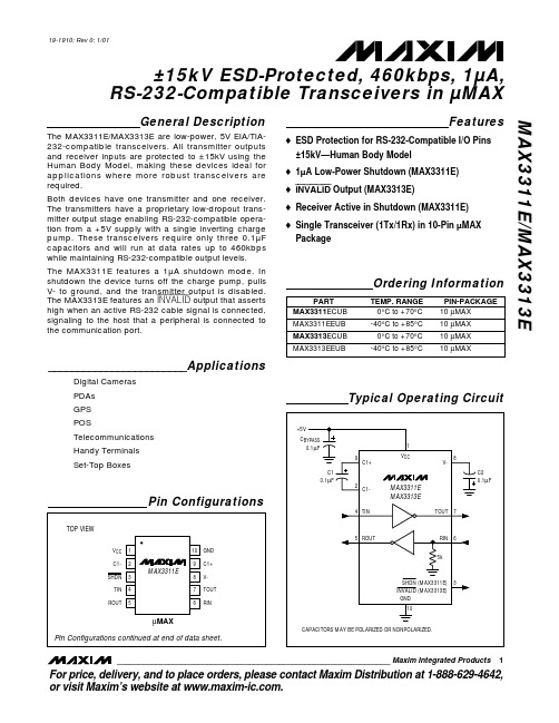
General DescriptionThe MAX3311E/MAX3313E are low-power, 5V EIA/TIA-232-compatible transceivers. All transmitter outputs and receiver inputs are protected to ±15kV using the Human Body Model, making these devices ideal for applications where more robust transceivers are required.Both devices have one transmitter and one receiver.The transmitters have a proprietary low-dropout trans-mitter output stage enabling RS-232-compatible opera-tion from a +5V supply with a single inverting charge pump. These transceivers require only three 0.1µF capacitors and will run at data rates up to 460kbps while maintaining RS-232-compatible output levels.The MAX3311E features a 1µA shutdown mode. In shutdown the device turns off the charge pump, pulls V- to ground, and the transmitter output is disabled.The MAX3313E features an INVALID output that asserts high when an active RS-232 cable signal is connected,signaling to the host that a peripheral is connected to the communication port.________________________ApplicationsDigital Cameras PDAs GPS POSTelecommunications Handy Terminals Set-Top BoxesFeatureso ESD Protection for RS-232-Compatible I/O Pins±15kV—Human Body Modelo 1µA Low-Power Shutdown (MAX3311E)o INVALID Output (MAX3313E)o Receiver Active in Shutdown (MAX3311E)o Single Transceiver (1Tx/1Rx) in 10-Pin µMAX PackageMAX3311E/MAX3313E±15kV ESD-Protected, 460kbps, 1µA,RS-232-Compatible Transceivers in µMAX________________________________________________________________Maxim Integrated Products1Pin Configurations19-1910; Rev 0; 1/01Ordering InformationFor price, delivery, and to place orders,please contact Maxim Distribution at 1-888-629-4642,or visit Maxim’s website at .Typical Operating CircuitM A X 3311E /M A X 3313E±15kV ESD-Protected, 460kbps, 1µA,RS-232-Compatible Transceivers in µMAX 2_______________________________________________________________________________________ABSOLUTE MAXIMUM RATINGSELECTRICAL CHARACTERISTICSStresses beyond those listed under “Absolute Maximum Ratings” may cause permanent damage to the device. These are stress ratings only, and functional operation of the device at these or any other conditions beyond those indicated in the operational sections of the specifications is not implied. Exposure to absolute maximum rating conditions for extended periods may affect device reliability.V CC to GND.............................................................-0.3V to +6V V- to GND................................................................+0.3V to -7V V CC + |V-|............................................................................+13V Input VoltagesTIN, SHDN to GND...............................................-0.3V to +6V RIN to GND......................................................................±25V Output VoltagesTOUT to GND................................................................±13.2V ROUT, INVALID to GND.....................…-0.3V to (V CC + 0.3V)Short-Circuit DurationTOUT to GND.........................................................ContinuousContinuous Power Dissipation10-Pin µMAX (derate 5.6mW/°C above +70°C)..........444mW Operating Temperature RangesMAX331_ECUB.................................................0°C to +70°C MAX331_EEUB..............................................-40°C to +85°C Junction Temperature.....................................................+150°C Storage Temperature Range............................-65°C to +150°C Lead Temperature (soldering, 10s)................................+300°CMAX3311E/MAX3313E±15kV ESD-Protected, 460kbps, 1µA,RS-232-Compatible Transceivers in µMAX_______________________________________________________________________________________3ELECTRICAL CHARACTERISTICS (continued)TIMING CHARACTERISTICSM A X 3311E /M A X 3313E±15kV ESD-Protected, 460kbps, 1µA,RS-232-Compatible Transceivers in µMAX 4_______________________________________________________________________________________Typical Operating Characteristics(V CC = +5V, 0.1µF capacitors, transmitter loaded with 3k Ωand C L , T A = +25°C, unless otherwise noted.)0428612101410001500500200025003000SLEW RATEvs. LOAD CAPACITANCELOAD CAPACITANCE (pF)S L E W R A T E (V /µs )-5-4-3-2-10123456050010001500200025003000TRANSMITTER OUTPUT VOLTAGEvs. LOAD CAPACITANCELOAD CAPACITANCE (pF)T R A N S M I T T E R O U T P U T V O L T A G E (V )010001500500200025003000SUPPLY CURRENT vs. LOAD CAPACITANCELOAD CAPACITANCE (pF)Detailed DescriptionSingle Charge-Pump Voltage ConverterThe MAX3311E/MAX3313E internal power supply has a single inverting charge pump that provides a negative voltage from a single +5V supply. The charge pump operates in a discontinuous mode and requires a flying capacitor (C1) and a reservoir capacitor (C2) to gener-ate the V- supply.RS-232-Compatible DriverThe transmitter is an inverting level translator that con-verts CMOS-logic levels to EIA/TIA-232 compatible lev-els. It guarantees data rates up to 460kbps with worst-case loads of 3k Ωin parallel with 1000pF. When SHDN is driven low, the transmitter is disabled and put into tri-state. The transmitter input does not have an internal pullup resistor.RS-232 ReceiverThe MAX3311E/MAX3313E receiver converts RS-232signals to CMOS-logic output levels. The MAX3311E receiver will remain active during shutdown mode. The MAX3313E INVALID indicates when an RS-232 signal is present at the receiver input, and therefore when the port is in use.The MAX3313E INVALID output is pulled low when no valid RS-232 signal level is detected on the receiver input.MAX3311E Shutdown ModeIn shutdown mode, the charge pump is turned off, V- is pulled to ground, and the transmitter output is disabled (Table 1). This reduces supply current typically to 1µA.The time required to exit shutdown is less than 25ms.Applications InformationCapacitor SelectionThe capacitor type used for C1 and C2 is not critical for proper operation; either polarized or nonpolarized capacitors are acceptable. If polarized capacitors are used, connect polarity as shown in the Typical Operating Circuit . The charge pump requires 0.1µF capacitors. Increasing the capacitor values (e.g., by a factor of 2) reduces power consumption. C2 can beincreased without changing C1’s value. However, do not increase C1’s value without also increasing the value of C2 and C BYPASS to maintain the proper ratios (C1 to the other capacitors).When using the minimum 0.1µF capacitors, make sure the capacitance does not degrade excessively with temperature. If in doubt, use capacitors with a larger nominal value. The capacitor ’s equivalent series resis-tance (ESR) usually rises at low temperatures and influ-ences the amount of ripple on V-.To reduce the output impedance at V-, use larger capacitors (up to 10µF).Bypass V CC to ground with at least 0.1µF. In applica-tions sensitive to power-supply noise generated by the charge pump, decouple V CC to ground with a capaci-tor the same size as (or larger than) charge-pump capacitors C1 and C2.Transmitter Output when ExitingShutdownFigure 1 shows the transmitter output when exiting shutdown mode. The transmitter is loaded with 3k Ωin parallel with 1000pF. The transmitter output displays no ringing or undesirable transients as the MAX3311E comes out of shutdown. Note that the transmitter is enabled only when the magnitude of V- exceeds approximately -3V.High Data RatesThe MAX3311E/MAX3313E maintain RS-232-compati-ble ±3.7V minimum transmitter output voltage even atMAX3311E/MAX3313E±15kV ESD-Protected, 460kbps, 1µA,RS-232-Compatible Transceivers in µMAX5Figure 1. Transmitter Output when Exiting Shutdown or Powering Up10µs/divSHDNTOUT5V/div1.5V/divTIN = GNDTIN = V CCM A X 3311E /M A X 3313E±15kV ESD-Protected, 460kbps, 1µA,RS-232-Compatible Transceivers in µMAX 6_______________________________________________________________________________________high data rates. Figure 2 shows a transmitter loopback test circuit. Figure 3 shows the loopback test result at 120kbps, and Figure 4 shows the same test at 250kbps.±15kV ESD ProtectionAs with all Maxim devices, ESD-protection structures are incorporated on all pins to protect against electro-static discharges encountered during handling and assembly. The MAX3311E/MAX3313E driver outputsand receiver inputs have extra protection against static discharge. Maxim ’s engineers have developed state-of-the-art structures to protect these pins against ESD of ±15kV without damage. The ESD structures withstand high ESD in all states: normal operation, shutdown, and powered down. After an ESD event, Maxim ’s E versions keep working without latchup; whereas, competing products can latch and must be powered down to remove latchup.ESD protection can be tested in various ways. The transmitter outputs and receiver inputs of the product family are characterized for protection to ±15kV using the Human Body Model.ESD Test ConditionsESD performance depends on a variety of conditions.Contact Maxim for a reliability report that documents test setup, test methodology, and test results.Human Body ModelFigure 5 shows the Human Body Model, and Figure 6shows the current waveform it generates when dis-charged into low impedance. This model consists of a 100pF capacitor charged to the ESD voltage of interest,which is then discharged into the test device through a 1.5k Ωresistor.Machine ModelThe Machine Model for ESD tests all pins using a 200pF storage capacitor and zero discharge resis-tance. Its objective is to emulate the stress caused by contact that occurs with handling and assembly during manufacturing. Of course, all pins require this protec-tion during manufacturing, not just RS-232 inputs and outputs. Therefore, after PC board assembly, the Machine Model is less relevant to I/O ports.Figure 4. Loopback Test Results at 250kbps2µs/divTOUTTINROUTFigure 3. Loopback Test Results at 120kbps 5µs/divTOUTTINROUTMAX3311E/MAX3313E±15kV ESD-Protected, 460kbps, 1µA,RS-232-Compatible Transceivers in µMAX_______________________________________________________________________________________7Figure 5. Human Body ESD Test ModelFigure 6. Human Body Current WaveformPin Configurations (continued)Chip InformationTRANSISTOR COUNT: 278M A X 3311E /M A X 3313E±15kV ESD-Protected, 460kbps, 1µA,RS-232-Compatible Transceivers in µMAX Maxim cannot assume responsibility for use of any circuitry other than circuitry entirely embodied in a Maxim product. No circuit patent licenses are implied. Maxim reserves the right to change the circuitry and specifications without notice at any time.8_____________________Maxim Integrated Products, 120 San Gabriel Drive, Sunnyvale, CA 94086 408-737-7600©2001 Maxim Integrated ProductsPrinted USAis a registered trademark of Maxim Integrated Products.______________________________________________________________Pin Description。
ASD863+651多协议多通道可编程智能交直流测试设备用户手册说明书

Leading Innovator in Power Testing Solution用户手册ASD863+651多协议多通道可编程智能交直流测试设备©版权归属于昂盛达电子股份有限公司Ver1.0/NOV,2020/ASD863+651注意事项◆感谢您购买和使用我司产品!本用户手册适用于ASD863+651交直流测试设备。
在使用前,请认真阅读本手册。
◆收到产品后请仔细检查产品外观、型号、合格证、用户手册及保修单等附件是否齐全。
若有问题请及时与经销商或我司联系;若发现产品外观破损,请勿通电使用,以免引发触电事故。
◆在使用过程中请严格遵守各项安全规范,若忽视或不遵守相关规范进行操作,将可能影响仪器性能,导致仪器损坏,甚至危及人身安全。
对不遵守安全规范而导致的任何后果,我司不予承担。
◆非专业人员请勿打开机箱,请勿擅自对仪器内部电路及元件进行更换或调整。
◆请在安全环境下使用,在通电前请确认输入电源的参数是否符合要求。
◆本手册所描述的可能并非产品的全部内容。
我司有权对本产品的性能、功能、内部结构、外观、附件等进行更改,对用户手册进行更新而不另行通知。
本手册最终解释权归我司所有。
◆客服电话:4001656165目录第一章验货安装 (4)1.1验货 (4)1.2清洁 (4)1.3连接部分的安装 (4)1.4安装尺寸................................................................................................................................错误!未定义书签。
1.5安装位置 (4)第二章快速入门 (4)2.1自检 (5)2.2负载仪前面板介绍 (6)2.3负载仪后面板介绍 (6)2.4功率计前面板介绍 (7)2.5功率计后面板介绍 (7)2.6测试治具介绍 (8)2.7触控屏介绍 (8)第三章技术规格 (9)第四章设备连接 (11)4.1测试设备环境搭建 (11)4.2待测试产品接口 (12)第五章基本操作 (13)5.1开机 (13)5.2研发模式 (14)5.3自动模式(A LONE测试模式) (16)5.4自动模式(2&2测试模式) (23)5.5自动模式(4IN1测试模式) (23)5.6其他设置 (24)第六章常见问题 (25)第七章保修协议 (26)简介ASD863+651交直流测试设备由ASD863多协议负载仪,ASD651PF数字功率计,安卓操作终端三部分组成,主要用于电源适配器等外接电源PCBA和成品的功能检测、参数测试及性能评估。
MAXIM的MAX31865温度检测器解决方案
MAXIM的MAX31865温度检测器解决方案简介MAXIM的MAX31865温度检测器是一款高精度、数字温度传感器。
它采用RTD传感器进行温度测量,支持多种RTD类型,如PT100和PT1000。
MAX31865还具有内置的线性化和数据过滤功能,可实现高精度温度测量和抗干扰能力。
MAX31865的主要特点•采用RTD传感器进行温度测量•支持多种RTD类型,如PT100和PT1000•内置线性化和数据过滤功能•支持SPI接口,通信速度高达10MHz•工作电压范围广泛,从3.0V到5.5V•支持低功耗模式,适用于移动、便携式应用MAX31865的应用领域MAX31865温度检测器广泛应用于以下领域: - 工业自动化 - 能源管理 - 环境监测 - 医疗设备 - 汽车电子MAX31865的电路设计原理MAX31865的电路设计包括三个主要部分:RTD传感器、MAX31865芯片和微控制器。
其中,RTD传感器负责温度测量,MAX31865芯片负责数据采集和处理,微控制器负责数据显示和传输。
以下是MAX31865电路设计的基本原理图:RTD传感器 MAX31865芯片微控制器| | |+---------------+----------------+|总线在这个电路中,RTD传感器连接到MAX31865芯片的输入引脚。
MAX31865芯片对传感器信号进行放大、滤波和线性化处理,然后将其转换为数字信号,并通过SPI总线发送给微控制器。
微控制器将接收到的数字信号转换为温度值,并在显示屏上显示。
MAX31865的注意事项在使用MAX31865温度检测器时,需要注意以下几点:•要正确选择RTD传感器的类型和额定阻值•要正确设置MAX31865芯片的配置寄存器,以实现期望的温度测量精度和抗干扰能力•要正确连接MAX31865芯片和微控制器的SPI总线,并配置正确的通信参数•要避免将MAX31865芯片的引脚连接到错误的电压或环境下,以避免损坏芯片或影响测量精度结论MAXIM的MAX31865温度检测器是一款高精度、数字温度传感器,适用于工业自动化、能源管理、环境监测、医疗设备和汽车电子等领域。
3186BC393T016APA1中文资料

SpecificationsHighlightsOperating Temperature:RatedVoltage: Capacitance:Capacitance Tolerance:DC Leakage Current:Cold Impedence:Ripple Current Multipliers:Series Inductance:Life Endurance Test:Shelf Life:Vibration:Type 3186, 85 °C Best-Value, High-Capacitance, Aluminum.Choice of Potted or Rilled High-Vibration ConstructionBest Value Screw Terminal TypeType 3186 is available with the capacitor element potted in place for lowest-cost or secured by rills, spoon shaped dimples in the side of the can. Rilled construction offers the industry’s highest vibration and shock withstanding and excellent heat transfer into the sides and bot-tom of the can. Besides increasing ripple current handling, the rilled construction extends the great value of Type 3186 into military and transportation settings that require rugged mechanical capability. • Rilled cans withstand high shock and vibration.• Potted cans are the lowest cost screw-terminal type.• High ripple current capability • High capacitance per can–40 °C to 85 °C 16 to 500 Vdc 220 µF to 1.0 F–10% +75% up to 100 Vdc, –10 + 50% 200 Vdc & up≤6√CV µA (6 mA max.) at 5 minutes –20 °C multiple of 25 °C Z ≤ 8 for 16–50V, 4 for 63–100V, 3 for 150V and up.Ambient Temperature2,000 h at 85 °C and rated voltage∆Capacitance ±10%ESR 200% of limit DCL 100% of limit500 h @ 85 °C and no voltage∆Capacitance ±10% ESR 175% of limit DCL 200% of limit Potted: 10 to 55 Hz, 0.06” and 10g max, 1.5 h ea. of 2 axis Rilled: 10 to 55 Hz, 0.06” and 15g max, 1.5 h ea. of 2 axis45 °C55 °C65 °C75 °C85 °C2.24 2.001.731.41 1.00Frequency 60 Hz 120 Hz 300 Hz 1000 Hz ≥10 kHz 16–100 V 0.90 1.00 1.15 1.25 1.30200–500 V0.901.001.251.401.50case dia (in)ESL (nH)case dia (in)ESL (nH)1.375182.5271.7523329225Complies with the EU Directive2002/95/EC requirement restricting the use of Lead (Pb), Mercury (Hg),Cadmium (Cd), Hexavalent chromium (Cr(VI)), PolyBrominated Biphenyls (PBB) and PolyBrominated Diphenyl Ethers (PBDE).Case Dimensions, Uninsulated Bare CanCan Dimensions Insulation AddersDiameter (D)Length (L)Standing Height (H)(in)(mm )(in)(mm )(in)(mm )0.008" PVC 0.020.510.0320.810.0240.610.012" PVC0.030.630.0621.580.0451.14Diam. (D) Length (L)Terminal Space(P)OptionalBracket Part No.Case ±0.031 ±0.8±0.062 ±1.6±0.014 ±0.4Vent Plug (A)Typical WeightCode (in)(mm )(in)(mm )(in)(mm )(in)(mm )(oz )(g)BA 1.37534.9 2.12554.00.512.70.398.0 2.572115058-06BB 1.37534.9 2.62566.70.512.70.398.0 3.290115058-06BC 1.37534.9 3.12579.40.512.70.398.0 3.7105115058-06BD 1.37534.9 3.62592.10.512.70.398.0 4.2120115058-06BE 1.37534.9 4.125104.80.512.70.398.0 4.7135115058-06BF 1.37534.9 4.625117.50.512.70.398.0 6.0170115058-06BG 1.37534.9 5.125130.20.512.70.398.07.7220115058-06BH 1.37534.9 5.625142.90.512.70.398.09.5270115058-06DA 1.75044.5 2.12554.00.7519.10.45311.5 5.6160115058-15DB 1.75044.5 2.62566.70.7519.10.45311.5 6.1175115058-15DC 1.75044.5 3.12579.40.7519.10.45311.5 6.3180115058-15DD 1.75044.5 3.62592.10.7519.10.45311.57.2205115058-15DE 1.75044.5 4.125104.80.7519.10.45311.57.7220115058-15DF 1.75044.5 4.625117.50.7519.10.45311.58.2235115058-15DG 1.75044.5 5.125130.20.7519.10.45311.58.8250115058-15DH 1.75044.5 5.625142.90.7519.10.45311.59.5270115058-15EA 2.00050.8 2.12554.00.87522.20.512.7 6.0170115058-09EB 2.00050.8 2.62566.70.87522.20.512.7 6.3180115058-09EC 2.00050.8 3.12579.40.87522.20.512.7 6.7190115058-09ED 2.00050.8 3.62592.10.87522.20.512.77.7220115058-09EE 2.00050.8 4.125104.80.87522.20.512.78.9255115058-09EF 2.00050.8 4.625117.50.87522.20.512.710.2290115058-09EG 2.00050.8 5.125130.20.87522.20.512.711.2320115058-09EH 2.00050.8 5.625142.90.87522.20.512.712.3350115058-09FB 2.50063.5 2.62566.7 1.12528.60.62515.910.5300115058-14FC 2.50063.5 3.12579.4 1.12528.60.62515.913.0370115058-14FD 2.50063.5 3.62592.1 1.12528.60.62515.914.0400115058-14FE 2.50063.5 4.125104.8 1.12528.60.62515.915.6445115058-14FF 2.50063.5 4.625117.5 1.12528.60.62515.921.0600115058-14FG 2.50063.5 5.125130.2 1.12528.60.62515.922.8650115058-14FH 2.50063.5 5.625142.9 1.12528.60.62515.921.0600115058-14GC 3.00076.2 3.12579.4 1.2531.80.7519.018.2520115058-11GD 3.00076.2 3.62592.1 1.2531.80.7519.020.0570115058-11GE 3.00076.2 4.125104.8 1.2531.80.7519.021.0600115058-11GF 3.00076.2 4.625117.5 1.2531.80.7519.025.2720115058-11GG 3.00076.2 5.125130.2 1.2531.80.7519.029.8850115058-11GH 3.00076.2 5.625142.9 1.2531.80.7519.034.0970115058-11GJ 3.00076.2 5.825148.0 1.2531.80.7519.036.81050115058-11GN3.00076.28.625219.11.2531.80.7519.051.11460115058-11Part Numbering System3186Type GHCase Code 562Capacitance 562=5600 µF 223=22000 µF 821=820 µF TToleranceM= ±20%S= –10 +30%T= –10 +50%U= –10 +75%400Voltage016=16 Vdc 450=450 Vdc MTerminalA=high post B=low post D=high currentlow post K=high current high postM=M5 high post J=M6 low post PInsulation P=0.008” PVC H=0.012” PVC N=noneWith mounting clamp/bracket:R=0.008” PVC J=0.012” PVC X=noneA1Construction *A1=potted R1=rilled S1=stud & potted**T1=stud & rilled*** Construction code is also a sequence number, e.g., A1, A2,---,A9, B1,B2,---,for customer specifications. Sequence number 1 in A1, R1, S1 and T1 denotesthe standard catalog capacitor with no special requirements.**Mounting stud not available for 1.375” diameter cases.Outline DrawingFor CasePost Diameter H max min Full Thread Torque Terminal Style Diameters Code inmminmm Threadin mm in·lb N·m Low Post 1⅜ to 3B 0.3148.00.094 2.410–320.218 5.525 2.82High Post 1⅜ to 3A 0.3148.00.2817.110–320.3759.525 2.82High Current, Low 2½ & 3D 0.68417.40.125 3.2¼–280.3448.760 6.78High Current, High 2½ & 3K 0.68417.40.2817.1¼–280.46911.960 6.78M5 Post, Small 1⅜ to 2M 0.3148.00.2817.1M50.3759.525 2.82M6 Low Post3J0.68417.40.125 3.2M60.3448.7606.78Terminal DimensionsClick here to see Hardware & Mounting OptionsRatingsCap. (µF)ESR max120 Hz, 25°C(mΩ)Ripple max120 Hz, 85 °Cpotted(A) rilled(A)Case SizeDxL(in)Cap.(µF)ESR max120 Hz, 25°C(mΩ)Ripple max120 Hz, 85 °Cpotted(A) rilled(A)Case SizeDxL(in) CatalogPart NumberCatalogPart Number16 Volts (20 Volts Surge)50 Volts (63 Volts Surge)220003186BA223T016APA125.0 4.7 5.4 1.375 X 2.12582003186BA822T050APA141.0 3.7 4.2 1.375 X 2.125 390003186BC393T016APA118.0 6.87.6 1.375 X 3.125120003186BC123T050APA128.0 5.4 6.0 1.375 X 3.125 560003186BE563T016APA114.08.89.7 1.375 X 4.125180003186BE183T050APA121.07.17.8 1.375 X 4.125 820003186EC823T016APA1 6.015.617.0 2.00 X 3.125270003186EC273T050APA115.09.210.0 2.00 X 3.125 1200003186EE124T016APA1 5.018.621.0 2.00 X 4.125470003186EE473T050APA111.011.513.0 2.00 X 4.125 1500003186EF154T016APA1 4.020.723.0 2.00 X 4.625560003186EF563T050APA110.013.515.0 2.00 X 4.625 1500003186EH154T016APA1 4.022.825.0 2.00 X 5.625680003186EH683T050APA19.015.517.0 2.00 X 5.625 2200003186FE224T016APA1 4.023.827.0 2.50 X 4.125680003186FE683T050APA18.015.918.0 2.50 X 4.125 2700003186FF274T016APA1 4.025.729.0 2.50 X 4.625820003186FF823T050APA17.017.720.0 2.50 X 4.625 3300003186FH334T016DPA1 3.030.634.0 2.50 X 5.6251000003186FH104T050APA1 6.021.624.0 2.50 X 5.625 3300003186GE334T016DPA1 4.028.132.0 3.00 X 4.1251000003186GE104T050APA1 6.020.223.0 3.00 X 4.125 3900003186GF394T016DPA1 3.030.935.0 3.00 X 4.6251200003186GF124T050APA1 6.022.125.0 3.00 X 4.625 4700003186GH474T016DPA1 3.035.640.0 3.00 X 5.6251500003186GH154T050DPA1 5.026.730.0 3.00 X 5.625 8200003186GN824T016DPA1 3.046.450.0 3.00 X 8.6252200003186GN224T050DPA1 4.037.140.0 3.00 X 8.625 10000003186GN105T016DPA1 3.046.450.0 3.00 X 8.62563 Volts (75 Volts Surge)25 Volts (30 Volts Surge)47003186BA472T063APA142.0 3.7 4.2 1.375 X 2.125 180003186BA183T025APA125.0 4.7 5.4 1.375 X 2.12582003186BC822T063APA128.0 5.4 6.0 1.375 X 3.125 270003186BC273T025APA118.0 6.77.5 1.375 X 3.125120003186BE123T063APA121.07.28.0 1.375 X 4.125 390003186BE393T025APA114.08.19.0 1.375 X 4.125180003186EC183T063APA115.09.210.0 2.00 X 3.125 680003186EC683T025APA1 6.015.617.0 2.00 X 3.125270003186EE273T063APA111.011.513.0 2.00 X 4.125 1000003186EE104T025APA1 5.018.621.0 2.00 X 4.125330003186EF333T063APA110.013.515.0 2.00 X 4.625 1200003186EF124T025APA1 4.020.723.0 2.00 X 4.625390003186EH393T063APA19.014.616.0 2.00 X 5.625 1500003186EH154T025APA1 4.023.726.0 2.00 X 5.625470003186FE473T063APA18.015.918.0 2.50 X 4.125 1500003186FE154T025APA1 4.023.827.0 2.50 X 4.125560003186FF563T063APA17.017.720.0 2.50 X 4.625 1800003186FF184T025APA1 4.025.729.0 2.50 X 4.625680003186FH683T063APA1 6.021.624.0 2.50 X 5.625 2200003186FH224T025DPA1 3.027.931.0 2.50 X 5.625680003186GE683T063APA1 6.020.223.0 3.00 X 4.125 2200003186GE224T025DPA1 4.028.132.0 3.00 X 4.125820003186GF823T063APA1 6.022.125.0 3.00 X 4.625 2700003186GF274T025DPA1 3.030.935.0 3.00 X 4.6251000003186GH104T063DPA1 5.026.730.0 3.00 X 5.625 3300003186GH334T025DPA1 3.033.838.0 3.00 X 5.6251500003186GN154T063DPA1 4.037.140.0 3.00 X 8.625 5600003186GN564T025DPA1 3.046.450.0 3.00 X 8.62575 Volts (95 Volts Surge)40 Volts (50 Volts Surge)39003186BA392T075APA143.0 3.6 4.1 1.375 X 2.125 100003186BA103T040APA133.0 4.2 4.8 1.375 X 2.12568003186BC682T075APA129.0 5.3 5.9 1.375 X 3.125 150003186BC153T040APA119.0 6.67.4 1.375 X 3.125100003186BE103T075APA121.07.17.8 1.375 X 4.125 220003186BE223T040APA114.08.59.4 1.375 X 4.125150003186EC153T075APA115.09.210.0 2.00 X 3.125 390003186EC393T040APA17.013.715.0 2.00 X 3.125220003186EE223T075APA111.011.513.0 2.00 X 4.125 560003186EE563T040APA1 6.016.819.0 2.00 X 4.125270003186EF273T075APA110.013.515.0 2.00 X 4.625 680003186EF683T040APA1 5.018.921.0 2.00 X 4.625330003186EH333T075APA19.015.517.0 2.00 X 5.625 820003186EH823T040APA1 5.021.023.0 2.00 X 5.625330003186FE333T075APA18.015.918.0 2.50 X 4.125 1000003186FE104T040APA1 5.021.224.0 2.50 X 4.125390003186FF393T075APA17.017.720.0 2.50 X 4.625 1200003186FF124T040APA1 4.023.927.0 2.50 X 4.625560003186FH563T075APA1 6.020.723.0 2.50 X 5.625 1500003186FH154T040DPA1 4.027.931.0 2.50 X 5.625470003186GE473T075APA17.020.223.0 3.00 X 4.125 1500003186GE154T040APA1 4.025.529.0 3.00 X 4.125560003186GF563T075APA1 6.022.125.0 3.00 X 4.625 1800003186GF184T040DPA1 4.030.935.0 3.00 X 4.625820003186GH823T075APA1 5.025.829.0 3.00 X 5.625 2200003186GH224T040DPA1 3.032.937.0 3.00 X 5.6251200003186GN124T075DPA1 4.037.140.0 3.00 X 8.625 3300003186GN334T040DPA1 3.046.450.0 3.00 X 8.625Cap. (µF)ESR max120 Hz, 25°C(mΩ)Ripple max120 Hz, 85 °Cpotted(A) rilled(A)Case SizeDxL(in)Cap.(µF)ESR max120 Hz, 25°C(mΩ)Ripple max120 Hz, 85 °Cpotted(A) rilled(A)Case SizeDxL(in) CatalogPart NumberCatalogPart Number100 Volts (125 Volts Surge)350 Volts (400 Volts Surge)27003186BA272T100APA165.0 2.9 3.3 1.375 X 2.12510003186BE102T350APA1112.0 3.0 3.30 1.375 X 4.125 39003186BC392T100APA150.0 3.8 4.3 1.375 X 3.12515003186EC152T350APA1105.0 3.6 3.90 2.00 X 3.125 56003186BE562T100APA132.0 5.3 5.9 1.375 X 4.12522003186EE222T350APA155.0 5.0 5.60 2.00 X 4.125 100003186EC103T100APA152.0 5.0 5.5 2.00 X 3.12527003186EF272T350APA144.0 6.37.00 2.00 X 4.625 150003186EE153T100APA137.0 6.57.3 2.00 X 4.12533003186EH332T350APA137.07.38.00 2.00 X 5.625 180003186EF183T100APA127.08.19.0 2.00 X 4.62527003186FE272T350APA154.0 5.8 6.60 2.50 X 4.125 220003186EH223T100APA111.013.715.0 2.00 X 5.62539003186FF392T350APA137.07.78.70 2.50 X 4.625 220003186FE223T100APA119.09.711.0 2.50 X 4.12547003186FH472T350APA133.08.69.60 2.50 X 5.625 270003186FF273T100APA116.011.513.0 2.50 X 4.62547003186GE472T350APA133.08.49.60 3.00 X 4.125 330003186FH333T100APA114.012.614.0 2.50 X 5.62556003186GF562T350APA133.08.810.00 3.00 X 4.625 330003186GE333T100APA114.012.314.0 3.00 X 4.12568003186GH682T350APA128.09.811.00 3.00 X 5.625 390003186GF393T100APA111.015.017.0 3.00 X 4.625120003186GN123T350APA118.016.718.00 3.00 X 8.625 560003186GH563T100DPA18.019.622.0 3.00 X 5.625400 Volts (450 Volts Surge)820003186GN823T100DPA17.023.225.0 3.00 X 8.6253303186BA331T400APA1290.0 1.1 1.3 1.375 X 2.125 200 Volts (250 Volts Surge)5603186BC561T400APA1190.0 1.9 2.1 1.375 X 3.125 10003186BA102T200APA1109.0 2.3 2.6 1.375 X 2.1258203186BE821T400APA1129.0 2.7 3.0 1.375 X 4.125 15003186BC152T200APA177.0 3.0 3.4 1.375 X 3.12512003186EC122T400APA195.0 3.4 3.7 2.00 X 3.125 22003186BE222T200APA152.0 4.2 4.6 1.375 X 4.12518003186EE182T400APA159.0 4.9 5.5 2.00 X 4.125 39003186EC392T200APA173.0 4.4 4.8 2.00 X 3.12522003186EF222T400APA150.0 5.7 6.4 2.00 X 4.625 56003186EE562T200APA124.07.68.6 2.00 X 4.12527003186EH272T400APA139.07.27.9 2.00 X 5.625 68003186EF682T200APA121.08.99.9 2.00 X 4.62527003186FE272T400APA148.0 6.47.3 2.50 X 4.125 82003186EH822T200APA117.011.012.0 2.00 X 5.62533003186FF332T400APA139.07.58.5 2.50 X 4.625 100003186FE103T200APA122.09.711.0 2.50 X 4.12539003186FH392T400APA137.08.59.4 2.50 X 5.625 120003186FF123T200APA117.010.612.0 2.50 X 4.62539003186GE392T400APA137.08.39.4 3.00 X 4.125 150003186FH153T200APA116.012.614.0 2.50 X 5.62547003186GF472T400APA134.08.810.0 3.00 X 4.625 120003186GE123T200APA126.09.711.0 3.00 X 4.12556003186GH562T400APA128.09.811.0 3.00 X 5.625 150003186GF153T200APA123.010.612.0 3.00 X 4.625100003186GN103T400APA118.016.718.0 3.00 X 8.625 220003186GH223T200APA117.013.415.0 3.00 X 5.625450 Volts (525 Volts Surge)330003186GN333T200APA115.015.817.0 3.00 X 8.6252203186BA221T450APA1430.00.9 1.0 1.375 X 2.125 250 Volts (300 Volts Surge)3903186BC391T450APA1310.0 1.6 1.8 1.375 X 3.125 6803186BA681T250APA1120.0 2.3 2.6 1.375 X 2.1255603186BE561T450APA1180.0 2.4 2.6 1.375 X 4.125 12003186BC122T250APA176.0 2.3 2.6 1.375 X 3.1258203186EC821T450APA1145.0 2.7 3.0 2.00 X 3.125 18003186BE182T250APA153.0 4.4 4.9 1.375 X 4.12512003186EE122T450APA185.0 4.1 4.6 2.00 X 4.125 27003186EC272T250APA167.0 4.0 4.4 2.00 X 3.12515003186EF152T450APA171.0 4.8 5.3 2.00 X 4.625 39003186EE392T250APA127.07.07.9 2.00 X 4.12518003186EH182T450APA160.0 5.4 5.9 2.00 X 5.625 47003186EF472T250APA123.08.19.0 2.00 X 4.62522003186FE222T450APA153.0 5.9 6.7 2.50 X 4.125 56003186EH562T250APA120.09.110.0 2.00 X 5.62527003186FF272T450APA145.0 6.87.7 2.50 X 4.625 68003186FE682T250APA124.08.810.0 2.50 X 4.12533003186FH332T450APA135.08.69.5 2.50 X 5.625 82003186FF822T250APA119.09.711.0 2.50 X 4.62533003186GE332T450APA135.08.39.5 3.00 X 4.125 100003186FH103T250APA117.012.614.0 2.50 X 5.62539003186GF392T450APA136.08.79.8 3.00 X 4.625 100003186GE103T250APA125.09.711.0 3.00 X 4.12547003186GH472T450APA131.09.811.0 3.00 X 5.625 120003186GF123T250APA122.010.612.0 3.00 X 4.62582003186GN822T450APA123.013.014.0 3.00 X 8.625 150003186GH153T250APA119.012.514.0 3.00 X 5.625500 Volts (550Volts Surge)220003186GN223T250APA116.015.817.0 3.00 X 8.6258203186EE821T500APA1132.0 3.0 3.4 2.00 X 4.125 350 Volts (400 Volts Surge)12003186EG122T500APA190.0 4.1 4.6 2.00 X 5.125 3903186BA391T350APA1270.0 1.1 1.3 1.375 X 2.12522003186FG222T500APA159.0 5.9 6.6 2.50 X 5.125 6803186BC681T350APA1163.0 2.2 2.5 1.375 X 3.12533003186GH332T500APA143.07.78.6 3.00 X 5.625。
基于MAX31865温度检测器的解决方案
基于MAX31865温度检测器的解决方案MAX31865是一款集成的的RTD数字转换器,单芯片解决方案,能替代多个分立元件来降低成本。
MAX31865提供简单而准确的测量温度,是在工业领域常用的测量值,因此非常适合用于测量和过程控制应用。
MAX31865是完全集成的RTD数字转换器,该单芯片方案可将系统成本降低50%,并可处理工业设计中常见的铂RTD (如Pt100或Pt1000)电阻数字转换问题。
该器件能够简便、准确地测量温度,是工业测量和过程控制的理想选择。
图1 参考原理图1图2 参考原理图2MAX31865主要特性•简单的数字值的转换铂RTD电阻•处理100Ω到1kΩ(0℃)PTRTD(PT100 PT1000)•适合于2、3和4线传感器连接•转换时间:最大21ms•15位ADC分辨率;额定温度分辨率0.03125℃(由于RTD非线性变化) •在所有操作条件下的总精度:0.5℃(0.05%满量程)•±50V的输入保护•全差分V REF输入•故障检测(开放式电阻元件、RTD输出范围电压、短路或短路电阻元件) •SPI兼容接口•20引脚TQFN封装MAX31865方案特点MAX31865评估板(EV套件)提供了评估MAX31865 RTD,数字转换器的硬件和软件(图形用户界面)。
EV套件包括,一个MAX31865ATP,以及一个USB至SPI接口。
图3 toplayer 图图4 bottomlayer 图评估套件的USB至SPI主控部分可以用于与MAX31865评估板软件互动,并执行设备的功能。
•轻松评估MAX31865•完全组装和测试•USB HID接口•评估板硬件是USB供电(包括USB 电缆)•Windows XP,Windows Vista的和Windows7兼容软件•符合RoHS标准•验证的PCB布局。
MAXIM MAX3185 数据手册

_______________General DescriptionThe MAX3185 is a complete DTE RS-232 serial port designed to meet the stringent ESD requirements of the European community. All transmitter outputs and receiv-er inputs are protected to ±15kV using IEC 1000-4-2 Air-Gap Discharge, ±8kV using IEC 1000-4-2 Contact Discharge, and ±15kV using the Human Body Model.The MAX3185 has three RS-232 transmitters, five RS-232 receivers, and no charge pump, optimizing it for operation in desktop PC and motherboard applications.It is guaranteed to run at data rates up to 230kbps, pro-viding compatibility with popular software for communi-cating with personal computers. Power-supply current is less than 300µA for I DD and I SS , and less than 1mA for I CC .The MAX3185 is pin and functionally compatible with the industry-standard 75185, so existing designs can instantly become EMC compliant. The MAX3185 is available in an SO package and in the tiny SSOP that further reduces board space.________________________ApplicationsDesktop PC Motherboards InstrumentsEquipment Meeting IEC1000-4-2____________________________Featureso Enhanced ESD Protection:±15kV—Human Body Model±8kV—IEC1000-4-2, Contact Discharge ±15kV—IEC1000-4-2, Air-Gap Discharge o Latchup Free During an ESD Event o 20-Pin SSOP and SO Packages o Guaranteed 230kbps Data Rate o Flow-Through Pinouto Pin Compatible with SN75C185o Complete DTE Serial PortMAX3185±15kV ESD-Protected, EMC-Compliant, 230kbps RS-232 Serial Port for Motherboards/Desktop PCs________________________________________________________________Maxim Integrated Products 1__________________Pin Configuration__________Typical Operating Circuit19-1076; Rev 0; 9/96______________Ordering InformationFor free samples & the latest literature: , or phone 1-800-998-8800M A X 3185±15kV ESD-Protected, EMC-Compliant, 230kbps RS-232 Serial Port for Motherboards/Desktop PCsABSOLUTE MAXIMUM RATINGSELECTRICAL CHARACTERISTICS(V CC = +4.5V to +5.5V, V DD = +10.8V to +13.2V, V SS = -10.8V to -13.2V, T A = T MIN to T MAX , unless otherwise noted. Typical values Stresses beyond those listed under “Absolute Maximum Ratings” may cause permanent damage to the device. These are stress ratings only, and functional operation of the device at these or any other conditions beyond those indicated in the operational sections of the specifications is not implied. Exposure to absolute maximum rating conditions for extended periods may affect device reliability.V CC ...........................................................................-0.3V to +7V V DD .........................................................................-0.3V to +14V V SS .........................................................................+0.3V to -14V Input VoltagesT IN ........................................................................-0.3V to +6V R IN ...................................................................................±30V Output VoltagesT OUT .................................................................................±15V R OUT .......................................................-0.3V to (V CC + 0.3V)Short-Circuit DurationT OUT (one at a time)...............................................Continuous R OUT (one at a time)..............................................ContinuousContinuous Power Dissipation (T A = +70°C)Wide SO (derate 10.00mW/°C above +70°C)..............800mW SSOP (derate 8.00mW/°C above +70°C)....................640mW Operating Temperature RangesMAX3185C_ P.....................................................0°C to +70°C MAX3185E_ P..................................................-40°C to +85°C Storage Temperature Range ............................-65°C to +160°C Lead Temperature (soldering, 10sec) ............................+300°CMAX3185±15kV ESD-Protected, EMC-Compliant, 230kbps RS-232 Serial Port for Motherboards/Desktop PCs_______________________________________________________________________________________3ELECTRICAL CHARACTERISTICS (continued)(V CC = +4.5V to +5.5V, V DD = +10.8V to +13.2V, V SS = -10.8V to -13.2V, T A = T MIN to T MAX , unless otherwise noted. Typical values are at T A = +25°C.)M A X 3185±15kV ESD-Protected, EMC-Compliant, 230kbps RS-232 Serial Port for Motherboards/Desktop PCs 4_________________________________________________________________________________________________________________________________Typical Operating Characteristics(V CC = +5.0V, V DD = +12.0V, V SS = -12.0V, T A = +25°C, unless otherwise noted.)-20SUPPLY CURRENT vs. SUPPLY VOLTAGESUPPLY VOLTAGE (V)S U P P L Y C U R E E N T (m A )-15-10-50510152013.212.612.011.410.8SUPPLY CURRENT vs. LOAD CAPACITANCELOAD CAPACITANCE (pF)S U P P L Y C U R E E N T (m A )2520151050-5-10-15-20-25400050003000200010000SLEW RATEvs. LOAD CAPACITANCELOAD CAPACITANCE (pF)S L E W R A T E (V /µs )1614121086420400050003000200010000TRANSMITTER OUTPUT VOLTAGEvs. LOAD CAPACITANCELOAD CAPACITANCE (pF)T R A N S M I T T E R O U T P U T V O L T A G E (V )400050003000200010000MAX3185 TRANSMITTER OUTPUT VOLTAGE vs. LOAD CURRENT PER TRANSMITTERLOAD CURRENT PER TRANSMITTER (mA)T R A N S M I T T E R O U T P U T V O L T A G E (V )101214161868240SLEW RATE vs. TEMPERATURETEMPERATURE (°C)S L E W R A T E (V /µs )2520151050851051254565525-35-15-55_______________Detailed Description±15kV ESD ProtectionAs with all Maxim devices, ESD-protection structures are incorporated on all pins to protect against electro-static discharges encountered during handling and assembly. The MAX3185 driver outputs and receiver inputs have extra protection against static electricity found in normal operation. Maxim’s engineers devel-oped state-of-the-art structures to protect these pins against ESD of ±15kV, without damage. After an ESD event, the MAX3185 continues working without latchup.ESD protection can be tested in several ways. The transmitter outputs and the receiver inputs are charac-terized for protection to the following:1)±15kV using the Human Body Model2)±8kV using the Contact-Discharge Method specified in IEC1000-4-2 (formerly IEC801-2)3)±15kV using the Air-Gap Method specified in IEC1000-4-2 (formerly IEC801-2)ESD Test ConditionsESD performance depends on a number of conditions.Contact Maxim for a reliability report that documents test setup, methodology, and results.MAX3185±15kV ESD-Protected, EMC-Compliant, 230kbps RS-232 Serial Port for Motherboards/Desktop PCs_______________________________________________________________________________________5______________________________________________________________Pin DescriptionPIN NAME FUNCTION1V DDSupply-Voltage Input, +10.8V to +13.2V 12, 14, 17, 18, 19R5OUT–R1OUT Receiver Outputs, swing between GND and V CC 16, 15, 13T3IN, T2IN, T1INTransmitter Inputs10V SS Supply-Voltage Input, -10.8V to -13.2V 11GND Ground. Connect system to ground.2, 3, 4, 7, 9R1IN–R5IN Receiver Inputs5, 6, 8T1OUT, T2OUT, T3OUTTransmitter Outputs, swing between V DD and V SS 20V CCSupply-Voltage Input, +4.5V to +5.5VFigure 1a. IEC1000-4-2 ESD Test ModelFigure 1b. IEC1000-4-2 ESD-Generator Current WaveformHuman Body ModelFigure 2a shows the Human Body Model, and Figure 2b shows the current waveform it generates when dis-charged into a low impedance. This model consists of a 100pF capacitor charged to the ESD voltage of inter-est, which is then discharged into the device through a 1.5k Ωresistor.IEC1000-4-2The IEC1000-4-2 standard covers ESD testing and per-formance of finished equipment; it does not specifically refer to integrated circuits. The MAX3185 helps you design equipment that meets Level 4 (the highest level)of IEC1000-4-2, without additional ESD-protection com-ponents.The main difference between tests done using the Human Body Model and IEC1000-4-2 is higher peak current in IEC1000-4-2. Because series resistance is lower in the IEC1000-4-2 ESD test model (Figure 1a),the ESD withstand voltage measured to this standard is generally lower than that measured using the Human Body Model. Figure 1b shows the current waveform for the ±8kV IEC1000-4-2 Level 4 ESD Contact-Discharge test.The Air-Gap test involves approaching the device with a charge probe. The Contact-Discharge method connects the probe to the device before the probe is energized.Machine ModelThe Machine Model for ESD testing uses a 200pF stor-age capacitor and zero-discharge resistance. It mimics the stress caused by handling during manufacturing and assembly. Of course, all pins (not just RS-232inputs and outputs) require this protection during man-ufacturing. Therefore, the Machine Model is less rele-vant to the I/O ports than are the Human Body Model and IEC1000-4-2.__________Applications InformationUse proper layout to ensure other devices on your board are not damaged in an ESD strike. Currents as high as 60A can instantaneously pass into ground, so be sure to minimize the ground-lead return path to the power supply. A separate return path to the power sup-ply is recommend. Trace widths should be greater than 40 mils. Bypass V CC , V DD , and V SS with 0.1µF capaci-tors as close to the part as possible to ensure maxi-mum ESD protection.Tie any unused transmitter inputs to GND or V CC . No external protection diodes are needed because the MAX3185 is not sensitive to power-supply sequencing.M A X 3185±15kV ESD-Protected, EMC-Compliant, 230kbps RS-232 Serial Port for Motherboards/Desktop PCs 6_______________________________________________________________________________________Figure 2a. Human Body ESD Test Model Figure 2b. Human Body Model Current WaveformMAX3185±15kV ESD-Protected, EMC-Compliant, 230kbps RS-232 Serial Port for Motherboards/Desktop PCs_______________________________________________________________________________________7TRANSISTOR COUNT: 217___________________Chip InformationFigure 3. Slew-Rate Test Circuit and Timing DiagramM A X 3185±15kV ESD-Protected, EMC-Compliant, 230kbps RS-232 Serial Port for Motherboards/Desktop PCs implied. Maxim reserves the right to change the circuitry and specifications without notice at any time.8___________________Maxim Integrated Products, 120 San Gabriel Drive, Sunnyvale, CA 94086 (408) 737-7600©1996 Maxim Integrated ProductsPrinted USAis a registered trademark of Maxim Integrated Products.________________________________________________________Package Information。
maxtec maxventuri 用户手册 - 中文(简体)说明书
866.4.Maxtec
I
警告
表示潜在的危险情况,如果不避免,可能导致死亡或严重损伤。
» 本器械不适于与生命支持器械/系统联用。 » 未遵从本手册中的警告或预防措施可能导致仪器损坏并威胁到患者和/或医护人员的福祉。 » 不正确使用本器械可能造成流量和氧气读数不准确,从而导致不正确的治疗、缺氧症或高氧
症、以及其他患者损伤或不适。请遵照本用户手册中概括的流程。
» 请勿在火焰、易燃/易爆物质、蒸气或氛围附近使用本器械。 在上述环境中操作氧气分析器
可能导致火灾或爆炸。 » 请勿在 MRI 环境中使用本器械。 » 本器械整体(包括电极)不适于在易燃麻醉剂混合物存在下或在易爆气体氛围中使用。 在上
述环境中操作氧气分析器可能导致火灾或爆炸。 » 如果 O2% 偏离了设定的水平,请检查患者界面的鼻腔插管未被痰液或鼻中隔堵塞。对回路或
患者界面的流量限制将导致氧气水平的升高。 对喉管的流量限制将不能被流量计检测出。 » 本器械在氧气供应中断时不会发出警报。 » 在调整氧气含量前确保氧气读数稳定。 » 本器械在氧气水平过高或过低时不会发出警报。 » 请勿在患者头部或颈部附近保留过长导管,以避免导致窒息。 » 请仅使用 Maxtec 替换传感器。 使用其他任何传感器将导致保修失效并可能导致产品损坏、
Maxtec 建议控制阀的 o 型环每 2 年更换或保养一次。
本保修不包含常规维护项目,如电池。对因使用后或因设备的滥用、误用、错误应用、改造、疏 忽或意外而造成的购买者或其他人的附带或后果损害,Maxtec 概不负责。
本有限产品保证取代所有其他明示或默示保证,包括但不限于适销性或特定目的适用性的任何默示 保证。
电话 (800) 748.5355 传真 (801) 270.5590 电子邮件:sales@ 网址:
MAX31865EVKIT

Required Equipment
● USB port
● Windows XP, Windows Vista, or Windows 7 PC ● Mini-USB cable (included) ● EV kit hardware (included) ● Micro screwdriver, bladed, size 0.4mm x 2.0mm x 60mm ● Jumper wire and a resistor (included) or an RTD (NOT included)
Note: Indicate that you are using the MAX31865 when contacting these component suppliers.
Quick Start
Note: In the following sections, software-related items are identified by bolding. Text in bold refers to items directly from the install or EV kit software. Text in bold and under lined refers to items from the Windows operating system.
Maxim Integrated │ 2
MAX31865 Evaluation Kit
Evaluates: MAX31865
Component Suppliers
SUPPLIER AVX Corporation Keystone Electronics Corp. Kingbright Corporation Molex Phoenix Contact ROHM Co., Ltd. TDK Corp. Vishay PHONE 843-946-0238 209-796-2032 909-468-0500 800-786-6539 800-808-7177 858-625-3630 847-803-6100 402-563-6866 WEBSITE
- 1、下载文档前请自行甄别文档内容的完整性,平台不提供额外的编辑、内容补充、找答案等附加服务。
- 2、"仅部分预览"的文档,不可在线预览部分如存在完整性等问题,可反馈申请退款(可完整预览的文档不适用该条件!)。
- 3、如文档侵犯您的权益,请联系客服反馈,我们会尽快为您处理(人工客服工作时间:9:00-18:30)。
VIL
CS, SDI, SCLK
Input Logic 1
Analog Voltages (FORCE+,FORCE2, FORCE-, RTDIN+, RTDIN-) Reference Resistor Cable Resistance
VIH
CS, SDI, SCLK
Normal conversion results
MAX31865 RTD-to-Digital Converter
ABSOLUTE MAXIMUM RATINGS
Voltage Range on VDD Relative to GND1.............-0.3V to +4.0V Voltage Range on BIAS, REFIN+,
Applications
Industrial Equipment Medical Equipment Instrumentation
Ordering Information appears at end of data sheet.
For related parts and recommended products to use with this part, refer to /MAX31865.related.
PACKAGE THERMAL CHARACTERISTICS (Note 1)
TQFN Junction-to-Ambient Thermal Resistance (qJA)...........29°C/W Junction-to-Case Thermal Resistance (qJC)..................2°C/W
EVALUATION KIT AVAILABLE
MAX31865 RTD-to-Digital Converter
General Description
The MAX31865 is an easy-to-use resistance-to-digital converter optimized for platinum resistance temperature detectors (RTDs). An external resistor sets the sensitivity for the RTD being used and a precision delta-sigma ADC converts the ratio of the RTD resistance to the reference resistance into digital form. The MAX31865’s inputs are protected against overvoltage faults as large as Q50V. Programmable detection of RTD and cable open and short conditions is included.
万联芯城专注电子元器件配单服务, 只售原装现货库存,万联芯城电子元器件全国供应,专 为终端生产,研发企业提供现货物料,价格优势明显, BOM配单整单采购可享优惠价,提交BOM表报价,最快 可当天发货,客户整单采购可节约采购时间,节省采购成本, 万联芯城产品体系能够满足多种电子元器件物料需求, 点击进入万联芯城。
Features
S Simple Conversion of Platinum RTD Resistance to Digital Value
S Handles 100Ω to 1kΩ (at 0°C) Platinum RTDs (PT100 to PT1000)
S Compatible with 2-, 3-, and 4-wire Sensor Connections S Conversion Time: 21ms max S 15-Bit ADC Resolution; Nominal Temperature
RTDIN+
RTDINFORCE-
RREF
RCABLE
RCABLE
CI*
RTD
RCABLE
RCABLE
*CI = 10nF FOR 1kΩ RTD 100nF FOR 100Ω RTD
Typical Application Circuits continued at end of data sheet.
Resolution 0.03125NC (Varies Due to RTD Nonlinearity) S Total Accuracy Over All Operating Conditions: 0.5NC (0.05% of Full Scale) max S ±50V Input Protection S Fully Differential VREF Inputs S Fault Detection (Open RTD Element, RTD Shorted to Out-of-Range Voltage, or Short Across RTD Element) S SPI-Compatible Interface S 20-Pin TQFN Package
FORCE-, RTDIN+, RTDIN- Relative to GND1.....-50V to +50V Voltage Range on DVDD Relative to DGND.........-0.3V to +4.0V Voltage Range on All Digital Pins
Stresses beyond those listed under “Absolute Maximum Ratings” may cause permanent damage to the device. These are stress ratings only, and functional operation of the device at these or any other conditions beyond those indicated in the operational sections of the specifications is not implied. Exposure to absolute maximum rating conditions for extended periods may affect device reliability.
PARAMETER ADC Resolution ADC Full-Scale Input Voltage (RTDIN+ - RTDIN-)
SYMBOL
CONDITIONS
No missing codes
MIN
TYP MAX UNITS
15
Bits
REFIN+ REFIN-
V
Maxim Integrated
2
MAX31865 RTD-to-Digital Converter
ELECTRICAL CHARACTERISTICS (continued)
(3.0V P VDD P 3.6V, TA = -40NC to +125NC, unless otherwise noted. Typical values are TA= +25NC, VDD = VDVDD = 3.3V.) (Notes 2 and 3)
Continuous Power Dissipation (TA = +70NC) TQFN (derate 34.5mW/NC above +70NC)...............2758.6mW
REFIN-, ISENSOR.................................. -0.3V to (VDD + 0.3V) Voltage Range on FORCE+, FORCE2,
For pricing, delivery, and ordering information, please contact Maxim Direct at 1-888-629-4642, or visit Maxim’s website at .
19-6478; Rev 0; 10/12
Relative to DGND.............................. -0.3V to (VDVDD + 0.3V)
ESD Protection (all pins, Human Body Model)....................±2kV Operating Temperature Range......................... -40NC to +125NC Junction Temperature......................................................+150NC Storage Temperature Range............................. -65NC to +150NC Soldering Temperature (reflow).......................................+260NC Lead Temperature (soldering,10s)..................................+300NC
Note 1: Package thermal resistances were obtained using the method described in JEDEC specification JESD51-7, using a four-layer board. For detailed information on package thermal considerations, refer to /thermal-tutorial.