STM32F103最小系统介绍
STM32F103__系列单片机介绍
STM32F103__系列单片机介绍《智能仪表》网络作业__03__系列单片机介绍__03__增强型系列由意法半导体集团设计,使用高性能的ARMCortex-M332位的RISC内核,工作频率为72MHz,内置髙速存储器(髙达128K字节的闪存和20K字节的SRAM),丰富的增强I/O端口和联接到两条APB总线的外设。
所有型号的器件都包含2个12位的ADC、3个通用16位定时器和一个PWM定时器,还包含标准和先进的通信接口:多达2个I2C和SPI、3个USART、一个USB和一个CAN。
1、结构与功能■内核:ARM32 位的Cortex?-M3CPU72MHz, 1.25DMips/MHz(Dhrystone2.1),0等待周期的存储器?支持单周期乘法和硬件除法■存储器从32K字节至512K字节的闪存程序存储器(__03—中的第二个x表示FLASH 容量,其中:“4”=16K,“6”=32K,“8”=64K,B=128K,C=256K, D=384K, E=512K) ?从6K 字节至64K 字节的SRAM ■时钟、复位和电源管理2.0至3.6伏供电和I/O管脚上电/断电复位(POR/PDR)、可编程电压监测器(PVD) ?内嵌4至16MHz髙速晶体振荡器?内嵌经出厂调校的8MHz的RC振荡器?内嵌40kHz的RC振荡器?PLL供应CPU时钟带校准功能的32kHzRTC 振荡器■低功耗?睡眠、停机和待机模式?VBAT 为RTC 和后备寄存器供电■2个12位模数转换器,1us转换时间(16通道)?转换范围:0至3.6V ?双采样和保持功能?温度传感器■DMA7 通道DMA 控制器支持的外设:定时器、ADC、SPI、I2C和USART ■多达80个快速I/O 口26/37/51/80 个多功能双向5V 兼容的I/O 口?所有I/O 口可以映像到16 个外部中断《智能仪表》网络作业■调试模式串行线调试(SWD)和JTAG接口■多达7个定时器多达3 个16 位定时器,每个定时器有多达4 个用于输入捕获/输出比较/PWM或脉冲计数的通道16 位6 通道高级控制定时器?多达6 路PWM 输出?死区控制、边缘/中间对齐波形和紧急制动 2 个看门狗定时器(独立的和窗口型的) ?系统时间定时器:24 位自减型■多达9 个通信接口多达 2 个I2C 接口(SMBus/PMBus)多达3 个USART 接口,支持__,LIN,IrDA 接口和调制解调控制? 多达2 个SPI 同步串行接口(18 兆位/秒) ?CAN 接口(2.0B 主动) ?USB2.0 全速接口■__?封装(兼容RoHS)2、特点概述ARM?的Cortex?-M3 核心ARM 的Cortex-M3 处理器是最新一代的嵌入式ARM 处理器,它为实现MCU 的需要提供了低成本的平台、缩减的管脚数目、降低的系统功耗,同时提供卓越的计算性能和先进的中断系统响应。
STM32F103最小系统

1 PIU?01
PIU?024
22
24 VDD_1 36 PIU?036 VDD_2 48 PIU?048 VDD_3
PIU?09
C
PID301
9
VDDA
8
STM32F103C8T6 GND VCC3.3
GND
VCC5
POWER COPOWER USB COUSB 1 VCC PIUSB01 2 D- PIUSB02 3 D+ PIUSB03 4 GND PIUSB04 D USB GND PL2303 DPL2303 D+ 1 2 GND
PIC1102 PIC1101
PIY102 COY1 PIY10
COD2 D2
1
Y1 8M
PA8 PA9 PA10 PA11 PA12 PA13/JTMS/SWDIO PA14/JTCK/SWCLK PA15/JTDI OSC_IN/PD0 OSC_OUT/PD1
R2 10k
PIQ102
COQ1 Q1
PIU?045
CORESET RESET
PIREST02
GND
BOOT1
COD1 D1 NLRESET RESET
PID101 PID102
COR1 R1 10k
PIR101
VCC3.3
PIR102
IN1418
PIR20 COR2
B
COC10 C10
PIC1002 PIC1001
22 GND
COC11 C11
\..\STM32F103
Sheet of Drawn By: .SchDoc 4
Bill of Materials
Source Data From: Project: Variant:
STM32F103VET6Mini最小系统
STM32F103VET6Mini最小系统
STM32F103VET6 Mini最小系统
产品简介:
这是一款基于STM32F103VET6为主芯片的ARM核心板,有如下特点:
1、板载了基于MCU的最基本电路,如晶振电路、USB电源管理电路和USB接口等。
2、核心板引出了所有的I/O口资源。
3、带有SWD仿真调试下载接口,该接口最少需要3根线就可以完成调试下载任务,相比传统的JTAG调试有不少的好处,在这里插一句,JTAG现在大有要淘汰的趋势,例如ST新出的M0系列的MCU 只保留了SWD调试接口,JTAG直接取消了。
4、使用了目前智能手机所使用的Mirco USB接口,使用方便,可做USB通讯和供电。
5、核心板的系统晶振(8MHz)使用精度极高质量上乘低负载NDK公司的NX5032G A,而没有使用价格低廉的铁壳晶振。
6、针对STM32 RTC不起振的问题,我们采用了官方建议的低负载RTC晶振方案,并使用了爱普生品牌的晶振,而没有使用廉价的圆柱晶振。
7、核心板配有EEPROM,型号为AT24C08方便核心板进行数据存储。
8、电源稳压芯片输入端和输出端分别放置了昂贵的大容量的钽电容,必将在稳压、滤波起着非同凡响的效果,同样我们还未在淘宝上找到比我们使用的容值更大的卖家,天地良心。
9、配有优质的2*24/2.54mm间距的双排排针,确保导电接触优良,方便用户将核心板放置到标准的的万用板或者面包板上。
排针默认不焊接,用户可以根据自己的需要选择焊接方向。
AltiumDesigner设计STM32F103最小系统
《电路设计与PCB制板》设计报告题目:STM32F103最小系统学院:专业:班级:姓名:学号:引言:Altium Designer基于一个软件集成平台,把为电子产品开发提供完整环境所需工具全部整合在一个应用软件中。
Altium Designer 包含所有设计任务所需工具:原理图和PCB设计、基于FPGA的嵌入式系统设计和开发。
目前我们使用到的功能特点主要有以下几点:1、提供了丰富的原理图组件和PCB封装库并且为设计新的器件提供了封装,简化了封装设计过程。
2、提供了层次原理图设计方法,支持“自上向下”的设计思想,使大型电路设计的工作组开发方式称为可能。
3、提供了强大的查错功能,原理图中的ERC(电气规则检查)工具和PCB 的DRC(设计规则检查)工具能帮助设计者更快的查出和改正错误。
4、全面兼容Protel系列以前的版本,并提供orcad格式文件的转换。
一、课程设计目的1、培养学生掌握、使用实用电子线路、计算机系统设计、制板的能力;2.提高学生读图、分析线路和正确绘制设计线路、系统的能力;3.了解原理图设计基础、了解设计环境设置、学习 Altium Designer 软件的功能及使用方法;4.掌握绘制原理图的各种工具、利用软件绘制原理图;5.掌握编辑元器件的方法构造原理图元件库;6. 熟练掌握手工绘制电路版的方法,并掌握绘制编辑元件封装图的方法,自己构造印制板元件库;7.了解电路板设计的一般规则、利用软件绘制原理图并自动生成印制板图。
二、设计过程规划1、根据实物板设计方案;2、制作原理图组件;3、绘制原理图;4、选择或绘制元器件的封装;5、导入PCB图进行绘制及布线;6、进入DRC检查;三、原理图绘制✧新建工程:1.在菜单栏选择File → New → Project → PCB Project2.Projects面板出现。
3.重新命名项目文件。
✧新建原理图纸1. 单击File → New→ Schematic,或者在Files面板的New 单元选择:Schematic Sheet。
STM32F103C8T6中文资料_引脚图_最小系统
Contents STM32F103x8,STM32F103xB Contents1Introduction (9)2Description (9)2.1Device overview (10)2.2Full compatibility throughout the family (13)2.3Overview (14)2.3.1ARM®Cortex™-M3core with embedded Flash and SRAM (14)2.3.2Embedded Flash memory (14)2.3.3CRC(cyclic redundancy check)calculation unit (14)2.3.4Embedded SRAM (14)2.3.5Nested vectored interrupt controller(NVIC) (14)2.3.6External interrupt/event controller(EXTI) (15)2.3.7Clocks and startup (15)2.3.8Boot modes (15)2.3.9Power supply schemes (15)2.3.10Power supply supervisor (15)2.3.11Voltage regulator (16)2.3.12Low-power modes (16)2.3.13DMA (17)2.3.14RTC(real-time clock)and backup registers (17)2.3.15Timers and watchdogs (17)2.3.16I²C bus (19)2.3.17Universal synchronous/asynchronous receiver transmitter(USART)..192.3.18Serial peripheral interface(SPI) (19)2.3.19Controller area network(CAN) (19)2.3.20Universal serial bus(USB) (19)2.3.21GPIOs(general-purpose inputs/outputs) (20)2.3.22ADC(analog-to-digital converter) (20)2.3.23T emperature sensor (20)2.3.24Serial wire JTAG debug port(SWJ-DP) (20)3Pinouts and pin description (21)4Memory mapping (34)2/105DocID13587Rev16STM32F103x8,STM32F103xB Contents5Electrical characteristics (35)5.1Parameter conditions (35)5.1.1Minimum and maximum values (35)5.1.2Typical values (35)5.1.3Typical curves (35)5.1.4Loading capacitor (35)5.1.5Pin input voltage (35)5.1.6Power supply scheme (36)5.1.7Current consumption measurement (37)5.2Absolute maximum ratings (37)5.3Operating conditions (38)5.3.1General operating conditions (38)5.3.2Operating conditions at power-up/power-down (39)5.3.3Embedded reset and power control block characteristics (40)5.3.4Embedded reference voltage (41)5.3.5Supply current characteristics (41)5.3.6External clock source characteristics (51)5.3.7Internal clock source characteristics (55)5.3.8PLL characteristics (57)5.3.9Memory characteristics (57)5.3.10EMC characteristics (58)5.3.11Absolute maximum ratings(electrical sensitivity) (60)5.3.12I/O current injection characteristics (61)5.3.13I/O port characteristics (62)5.3.14NRST pin characteristics (68)5.3.15TIM timer characteristics (69)5.3.16Communications interfaces (70)5.3.17CAN(controller area network)interface (75)5.3.1812-bit ADC characteristics (76)5.3.19T emperature sensor characteristics (80)6Package characteristics (81)6.1Package mechanical data (81)6.2Thermal characteristics (93)6.2.1Reference document (93)6.2.2Selecting the product temperature range (94)DocID13587Rev163/105Contents STM32F103x8,STM32F103xB7Ordering information scheme (96)8Revision history (97)4/105DocID13587Rev16STM32F103x8,STM32F103xB List of tables List of tablesT able1.Device summary (1)T able2.STM32F103xx medium-density device features and peripheral counts (10)T able3.STM32F103xx family (13)T able4.Timer feature comparison (17)T able5.Medium-density STM32F103xx pin definitions (28)T able6.Voltage characteristics (37)T able7.Current characteristics (38)T able8.Thermal characteristics (38)T able9.General operating conditions (38)T able10.Operating conditions at power-up/power-down (39)T able11.Embedded reset and power control block characteristics (40)T able12.Embedded internal reference voltage (41)T able13.Maximum current consumption in Run mode,code with data processingrunning from Flash (42)T able14.Maximum current consumption in Run mode,code with data processingrunning from RAM (42)T able15.Maximum current consumption in Sleep mode,code running from Flash or RAM (44)T able16.Typical and maximum current consumptions in Stop and Standby modes (45)T able17.Typical current consumption in Run mode,code with data processingrunning from Flash (48)T able18.Typical current consumption in Sleep mode,code running from Flash orRAM (49)T able19.Peripheral current consumption (50)T able20.High-speed external user clock characteristics (51)T able21.Low-speed external user clock characteristics (51)T able22.HSE4-16MHz oscillator characteristics (53)T able23.LSE oscillator characteristics(f LSE=32.768kHz) (54)T able24.HSI oscillator characteristics (55)T able25.LSI oscillator characteristics (56)T able26.Low-power mode wakeup timings (57)T able27.PLL characteristics (57)T able28.Flash memory characteristics (57)T able29.Flash memory endurance and data retention (58)T able30.EMS characteristics (59)T able31.EMI characteristics (59)T able32.ESD absolute maximum ratings (60)T able33.Electrical sensitivities (60)T able34.I/O current injection susceptibility (61)T able35.I/O static characteristics (62)T able36.Output voltage characteristics (66)T able37.I/O AC characteristics (67)T able38.NRST pin characteristics (68)T able39.TIMx characteristics (69)T able40.I2C characteristics (70)T able41.SCL frequency(f PCLK1=36MHz.,V DD_I2C=3.3V) (71)T able42.SPI characteristics (72)T B startup time (74)T B DC electrical characteristics (75)DocID13587Rev165/105List of tables STM32F103x8,STM32F103xBT B:Full-speed electrical characteristics (75)T able46.ADC characteristics (76)T able47.R AIN max for f ADC=14MHz (77)T able48.ADC accuracy-limited test conditions (77)T able49.ADC accuracy (78)T able50.TS characteristics (80)T able51.VFQFPN366x6mm,0.5mm pitch,package mechanical data (82)T able52.UFQFPN487x7mm,0.5mm pitch,package mechanical data (83)T able53.LFBGA100-10x10mm low profile fine pitch ball grid array packagemechanical data (85)T able54.LQPF100,14x14mm100-pin low-profile quad flat package mechanical data (87)T able55.UFBGA100-ultra fine pitch ball grid array,7x7mm,0.50mm pitch,packagemechanical data (88)T able56.LQFP64,10x10mm,64-pin low-profile quad flat package mechanical data (89)T able57.TFBGA64-8x8active ball array,5x5mm,0.5mm pitch,package mechanical data (90)T able58.LQFP48,7x7mm,48-pin low-profile quad flat package mechanical data (92)T able59.Package thermal characteristics (93)T able60.Ordering information scheme (96)T able61.Document revision history (97)6/105DocID13587Rev16STM32F103x8,STM32F103xB List of figures List of figuresFigure1.STM32F103xx performance line block diagram (11)Figure2.Clock tree (12)Figure3.STM32F103xx performance line LFBGA100ballout (21)Figure4.STM32F103xx performance line LQFP100pinout (22)Figure5.STM32F103xx performance line UFBGA100pinout (23)Figure6.STM32F103xx performance line LQFP64pinout (24)Figure7.STM32F103xx performance line TFBGA64ballout (25)Figure8.STM32F103xx performance line LQFP48pinout (26)Figure9.STM32F103xx performance line UFQFPN48pinout (26)Figure10.STM32F103xx performance line VFQFPN36pinout (27)Figure11.Memory map (34)Figure12.Pin loading conditions (36)Figure13.Pin input voltage (36)Figure14.Power supply scheme (36)Figure15.Current consumption measurement scheme (37)Figure16.Typical current consumption in Run mode versus frequency(at3.6V)-code with data processing running from RAM,peripherals enabled (43)Figure17.Typical current consumption in Run mode versus frequency(at3.6V)-code with data processing running from RAM,peripherals disabled (43)Figure18.Typical current consumption on V BAT with RTC on versus temperature at differentV BAT values (45)Figure19.Typical current consumption in Stop mode with regulator in Run mode versustemperature at V DD=3.3V and3.6V (46)Figure20.Typical current consumption in Stop mode with regulator in Low-power mode versustemperature at V DD=3.3V and3.6V (46)Figure21.Typical current consumption in Standby mode versus temperature atV DD=3.3V and3.6V (47)Figure22.High-speed external clock source AC timing diagram (52)Figure23.Low-speed external clock source AC timing diagram (52)Figure24.Typical application with an8MHz crystal (53)Figure25.Typical application with a32.768kHz crystal (55)Figure26.Standard I/O input characteristics-CMOS port (64)Figure27.Standard I/O input characteristics-TTL port (64)Figure28.5V tolerant I/O input characteristics-CMOS port (65)Figure29.5V tolerant I/O input characteristics-TTL port (65)Figure30.I/O AC characteristics definition (68)Figure31.Recommended NRST pin protection (69)Figure32.I2C bus AC waveforms and measurement circuit (71)Figure33.SPI timing diagram-slave mode and CPHA=0 (73)Figure34.SPI timing diagram-slave mode and CPHA=1(1) (73)Figure35.SPI timing diagram-master mode(1) (74)B timings:definition of data signal rise and fall time (75)Figure37.ADC accuracy characteristics (78)Figure38.Typical connection diagram using the ADC (79)Figure39.Power supply and reference decoupling(V REF+not connected to V DDA) (79)Figure40.Power supply and reference decoupling(V REF+connected to V DDA) (80)Figure41.VFQFPN366x6mm,0.5mm pitch,package outline(1) (82)Figure42.VFQFPN36recommended footprint(dimensions in mm)(1)(2) (82)DocID13587Rev167/105List of figures STM32F103x8,STM32F103xBFigure43.UFQFPN487x7mm,0.5mm pitch,package outline (83)Figure44.UFQFPN48recommended footprint (84)Figure45.LFBGA100-10x10mm low profile fine pitch ball grid array packageoutline (85)Figure46.Recommended PCB design rules(0.80/0.75mm pitch BGA) (86)Figure47.LQFP100,14x14mm100-pin low-profile quad flat package outline (87)Figure48.LQFP100recommended footprint(1) (87)Figure49.UFBGA100-ultra fine pitch ball grid array,7x7mm,0.50mm pitch,package outline (88)Figure50.LQFP64,10x10mm,64-pin low-profile quad flat package outline (89)Figure51.LQFP64recommended footprint(1) (89)Figure52.TFBGA64-8x8active ball array,5x5mm,0.5mm pitch,package outline (90)Figure53.Recommended PCB design rules for pads(0.5mm pitch BGA) (91)Figure54.LQFP48,7x7mm,48-pin low-profile quad flat package outline (92)Figure55.LQFP48recommended footprint(1) (92)Figure56.LQFP100P D max vs.T A (95)8/105DocID13587Rev16STM32F103x8,STM32F103xB Introduction 1IntroductionThis datasheet provides the ordering information and mechanical device characteristics ofthe STM32F103x8and STM32F103xB medium-density performance line microcontrollers.For more details on the whole STMicroelectronics STM32F103xx family,please refer toSection2.2:Full compatibility throughout the family.The medium-density STM32F103xx datasheet should be read in conjunction with the low-,medium-and high-density STM32F10xxx reference manual.The reference and Flash programming manuals are both available from theSTMicroelectronics website .For information on the Cortex™-M3core please refer to the Cortex™-M3T echnicalReference Manual,available from the website at the following address:/help/index.jsp?topic=/com.arm.doc.ddi0337e/2DescriptionThe STM32F103xx medium-density performance line family incorporates the high-performance ARM Cortex™-M332-bit RISC core operating at a72MHz frequency,high-speed embedded memories(Flash memory up to128Kbytes and SRAM up to20Kbytes),and an extensive range of enhanced I/Os and peripherals connected to two APB buses.Alldevices offer two12-bit ADCs,three general purpose16-bit timers plus one PWM timer,aswell as standard and advanced communication interfaces:up to two I2Cs and SPIs,threeUSART s,an USB and a CAN.The devices operate from a2.0to3.6V power supply.They are available in both the–40to+85°C temperature range and the–40to+105°C extended temperature range.Acomprehensive set of power-saving mode allows the design of low-power applications.The STM32F103xx medium-density performance line family includes devices in six differentpackage types:from36pins to100pins.Depending on the device chosen,different sets ofperipherals are included,the description below gives an overview of the complete range ofperipherals proposed in this family.These features make the STM32F103xx medium-density performance line microcontrollerfamily suitable for a wide range of applications such as motor drives,application control,medical and handheld equipment,PC and gaming peripherals,GPS platforms,industrialapplications,PLCs,inverters,printers,scanners,alarm systems,video intercoms,andHVACs.DocID13587Rev169/105TimersCommunicationDescription STM32F103x8,STM32F103xB 2.1Device overviewTable2.STM32F103xx medium-density device features and peripheral1.On the TFBGA64package only15channels are available(one analog input pin has been replaced by‘Vref+’).10/105DocID13587Rev16Peripheral STM32F103Tx STM32F103Cx STM32F103Rx STM32F103Vx Flash-Kbytes64128641286412864128SRAM-Kbytes20202020 General-purpose3333Advanced-control1111SPI12222I C1222USART2333USB1111CAN1111 GPIOs2637518012-bit synchronized ADCNumber of channels210channels210channels2(1)16channels216channels CPU frequency72MHzOperating voltage 2.0to3.6VOperating temperaturesAmbient temperatures:-40to+85°C/-40to+105°C(see Table9)Junction temperature:-40to+125°C(see Table9)Packages VFQFPN36LQFP48,UFQFPN48LQFP64,TFBGA64LQFP100,LFBGA100,UFBGA100f l a s ho b lI n t e r f a c eB u s M a t r i xA HB :F m a x =48/72M H zA PB 2:F m a x =48/72M H zA PB 1:F m a x =24/36M H zpbusPCLK2 HCLK CLOCK RTC AWUTAMPER -RTCSTM32F103x8, STM32F103xBDescriptionFigure 1. STM32F103xx performance line block diagramTRACECLKTRACED[0:3] as ASNJTRSTTRSTJTDIJTCK/SWCLK JTMS/SWDIOJTDO as AFTPIUTrace/trigSW/JTAGCortex -M3 CPUIbusF max : 7 2M Hz DbusTraceControlle rFlash 128 KB64 bitPOWERVOLT. REG. 3.3V TO 1.8V@VDDV DD = 2 to 3.6VV SSNVICSystemSRAM20 KB@VDDGP DMA7 channelsPCLK1 FCLKPLL &MANAGTXTAL OSC4-16 MHzOSC_INOSC_OUTRC 8 MHzNRST @VDDASUPPLYSUPERVISIONRC 40 kHz @VDDA@VBATIWDG Standby interfaceV BATVDDA VSSA 80AF PA[15:0] PB[15:0]POR / PDRPVDEXTIWAKEUPGPIOAGPIOBRstIntAHB2 AHB2APB2 APB1XTAL 32 kHzBackup reg Backu p i nterf ace TIM2 TIM3OSC32_IN OSC32_OUT4 Channels 4 ChannelsPC[15:0]GPIOCTIM 44 ChannelsPD[15:0]GPIOD PE[15:0] GPIOEUSART2USART3RX,TX, CTS, RTS,CK, SmartCard as AFRX,TX, CTS, RTS, CK, SmartCard as AF4 Channels3 compl. ChannelsETR and BKINMOSI,MISO, SCK,NSS as AFRX,TX, CTS, RTS,TIM1SPI12x(8x16bit)SPI2I2C1 I2C2MOSI,MISO,SCK,NSS as AFSCL,SDA,SMBA as AFSCL,SDA as AFSmartCard as AFUSART1@VDDAbxCANUSBDP/CAN_TXUSB 2.0 FSUSBDM/CAN_RX16AF V REF+ V REF -12bit ADC1 IF12bit ADC2 IFSRAM 512BWWDGTemp sensorai14390d1. T A = –40 °C to +105 °C (junction temperature up to 125 °C).2. AF = alternate function on I/O port pin.DocID13587 Rev 1611/105peripheralsIf (APB2 prescaler =1) x1 ADC /2, 4, 6, 8 ADCCLKDescriptionSTM32F103x8, STM32F103xBFigure 2. Clock treeFLITFCLKto Flash programming interface8 MHz HSI RCHSIUSBPrescaler 48 MHzUSBCLKto USB interface/2/1, 1.572 MHz maxClockHCLKto AHB bus, core, memory and DMA PLLSRCSWPLLMUL/8Enable (3 bits)to Cortex System timerFCLK Cortex..., x16 x2, x3, x4 PLLHSIPLLCLK HSESYSCLK72 MHz max AHB Prescaler /1, 2..512 APB1Prescaler/1, 2, 4, 8, 16free running clock36 MHz max PCLK1to APB1Peripheral Clock Enable (13 bits)TIM2,3, 4to TIM2, 3and 4CSSIf (APB1 prescaler =1) x1 TIMXCLKelse x2 Peripheral ClockEnable (3 bits)OSC_OUTOSC_IN4-16 MHzHSE OSCPLLXTPRE/2APB2Prescaler/1, 2, 4, 8, 16TIM1 timer 72 MHz maxPeripheral ClockEnable (11 bits) PCLK2peripherals to APB2to TIM1 TIM1CLK else x2 Peripheral ClockOSC32_INOSC32_OUTLSE OSC32.768 kHz/128LSERTCCLKto RTCPrescaler Enable (1 bit) to ADCRTCSEL[1:0]LSI RCLSIto Independent Watchdog (IWDG)40 kHzIWDGCLKLegend:HSE = high -speed external clock signalHSI = high -speed internal clock signalMCOMainClock Output/2PLLCLKHSI LSI = low -speed internal clock signal LSE = low -speed external clock signalHSESYSCLKMCOai149031. When the HSI is used as a PLL clock input, the maximum system clock frequency that can be achieved is 64 MHz.2. For the USB function to be available, both HSE and PLL must be enabled, with USBCLK running at 48 MHz.3. To have an ADC conversion time of 1 µs, APB2 must be at 14 MHz, 28 MHz or 56 MHz.12/105DocID13587 Rev 16STM32F103x8, STM32F103xBDescription2.2 Full compatibility throughout the familyThe STM32F103xx is a complete family whose members are fully pin -to -pin, software and feature compatible. In the reference manual, the STM32F103x4 and STM32F103x6 are identified as low -density devices, the STM32F103x8 and STM32F103xB are referred to as medium -density devices, and the STM32F103xC, STM32F103xD and STM32F103xE are referred to as high -density devices.Low - and high -density devices are an extension of the STM32F103x8/B devices, they are specified in the STM32F103x4/6 and STM32F103xC/D/E datasheets, respectively. Low - density devices feature lower Flash memory and RAM capacities, less timers and peripherals. High -density devices have higher Flash memory and RAM capacities, and additional peripherals like SDIO, FSMC, I 2S and DAC, while remaining fully compatible with the other members of the STM32F103xx family .The STM32F103x4, STM32F103x6, STM32F103xC, STM32F103xD and STM32F103xE are a drop -in replacement for STM32F103x8/B medium -density devices, allowing the user to try different memory densities and providing a greater degree of freedom during the development cycle.Moreover, the STM32F103xx performance line family is fully compatible with all existing STM32F101xx access line and STM32F102xx USB access line devices.1.For orderable part numbers that do not show the A internal code after the temperature range code (6 or 7),the reference datasheet for electrical characteristics is that of the STM32F103x8/B medium -density devices.DocID13587 Rev 16 13/105PinoutLow -density devicesMedium -density devices High -density devices 16 KB Flash 32 KB Flash (1) 64 KB Flash 128 KB Flash 256 KB Flash 384 KB Flash 512 KB Flash6 KB RAM 10 KB RAM 20 KB RAM 20 KB RAM 48 KB RAM 64 KB RAM 64 KB RAM144 5 × USART s 4 × 16-bit timers, 2 × basic timers2 3 × SPIs, 2 × I Ss, 2 × I2Cs USB, CAN, 2 × PWM timers 3 × ADCs, 2 × DACs, 1 × SDIOFSMC (100 and 144 pins) 100 3 × USART s 3 × 16-bit timers 2 2 × SPIs, 2 × I Cs, USB, CAN, 1 × PWM timer2 × ADCs 64 2 × USART s 2 × 16-bit timers 2 1 × SPI, 1 × I C, USB, CAN, 1 × PWM timer 2 × ADCs 48 36Description STM32F103x8,STM32F103xB 2.3Overview2.3.1ARM®Cortex™-M3core with embedded Flash and SRAMThe ARM Cortex™-M3processor is the latest generation of ARM processors for embeddedsystems.It has been developed to provide a low-cost platform that meets the needs of MCUimplementation,with a reduced pin count and low-power consumption,while deliveringoutstanding computational performance and an advanced system response to interrupts.The ARM Cortex™-M332-bit RISC processor features exceptional code-efficiency,delivering the high-performance expected from an ARM core in the memory size usuallyassociated with8-and16-bit devices.The STM32F103xx performance line family having an embedded ARM core,is thereforecompatible with all ARM tools and software.Figure1shows the general block diagram of the device family.2.3.2Embedded Flash memory64or128Kbytes of embedded Flash is available for storing programs and data.2.3.3CRC(cyclic redundancy check)calculation unitThe CRC(cyclic redundancy check)calculation unit is used to get a CRC code from a32-bitdata word and a fixed generator polynomial.Among other applications,CRC-based techniques are used to verify data transmission orstorage integrity.In the scope of the EN/IEC60335-1standard,they offer a means ofverifying the Flash memory integrity.The CRC calculation unit helps compute a signature ofthe software during runtime,to be compared with a reference signature generated at link-time and stored at a given memory location.2.3.4Embedded SRAMTwenty Kbytes of embedded SRAM accessed(read/write)at CPU clock speed with0waitstates.2.3.5Nested vectored interrupt controller(NVIC)The STM32F103xx performance line embeds a nested vectored interrupt controller able tohandle up to43maskable interrupt channels(not including the16interrupt lines ofCortex™-M3)and16priority levels.•Closely coupled NVIC gives low-latency interrupt processing•Interrupt entry vector table address passed directly to the core•Closely coupled NVIC core interface•Allows early processing of interrupts•Processing of late arriving higher priority interrupts•Support for tail-chaining•Processor state automatically saved•Interrupt entry restored on interrupt exit with no instruction overhead14/105DocID13587Rev16万联芯城专注电子元器件配单服务,只售原装现货库存,万联芯城电子元器件全国供应,专为终端生产,研发企业提供现货物料,价格优势明显,BOM配单采购可节省逐个搜索购买环节,只需提交BOM物料清单,商城即可为您报价,解决客户采购烦恼,为客户节省采购成本,点击进入万联芯城。
STM32单片机最小系统详解
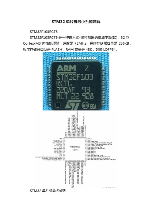
STM32单片机最小系统详解STM32F103RCT6:STM32F103RCT6是一种嵌入式-微控制器的集成电路(IC),32位Cortex-M3内核处理器,速度是72MHz,程序存储器容量是256KB,程序存储器类型是FLASH,RAM容量是48K,封装LQFP64。
STM32单片机命名规则:STM32单片机最小系统:所谓单片机最小系统,就是让单片机能够正常运行,最少且必须的器件所组成的系统。
单片机最小系统上电之后,单片机可以正常复位,下载程序,除此之外没有其他任何功能。
在最小系统保证正确的基础上,可以依次添加其他功能模块或器件,使之单片机具有实际功能。
STM32单片机最小系统包括一个复位电路和一个时钟电路。
如下图1所示。
图中复位电路使用的是上电复位电路,STM32单片机NRST引脚输入低电平,则发生复位。
图1 STM32F103单片机最小系统电源引脚:VDD是单片机的数字电源正极,VSS是数字电源负极,共有5个VDD引脚,5个VSS引脚。
VDDA是单片机的模拟电源正极,负责给内部的ADC、DAC模块供电,VSSA是模拟电源负极。
还有一个电源引脚,就是VBAT,BAT就是Battery(电池),这个引脚用来连接电池的正极的。
STM32带RTC功能(实时时钟),所以有VBAT引脚。
原理图上预留了一个CR1220纽扣锂电池,当主电源供电存在的情况下,由系统中的VCC3.3给VBAT供电;当主电源断电之后,由CR1220纽扣电池给STM32自带的RTC模块供电,从而能够保证实时时钟模块在主电源掉电的情况下还能够正常工作。
但是这样设计的话,这里有一个矛盾需要解决。
如果VBAT引脚直接与VCC3.3和CR1220连接的话,会存在下面问题:1、当电池电压高于3.3V,电池就会输出电流到AMS1117,使得芯片发烫,还会很快消耗电池电量。
2、如果电池电压低于3.3V,AMS1117产生的3.3V,就会给电池充电,而这种CR1220电池是不能够充电的。
STM32最小系统使用手册
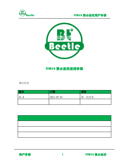
STM32最小系统使用手册修订历史1.STM32F103C8T6最小系统简介硬件资源:1、STM32F103C8主芯片一片2、贴片8M晶振(通过芯片内部PLL最高达72M)ST官方标准参数3、LM1117-3.3V稳压芯片,最大提供800mA电流4、一路miniUSB接口,可以给系统版供电,预留USB通讯功能5、复位按键6、标准JTAG下载口一个,支持JLink,STLink7、BOOT选择端口8、IO扩展排针20pin x 29、电源指示灯1个10、功能指示灯一个,用于验证IO口基本功能11、预留串口下载接口,方便和5V开发板连接,用串口即可下载程序12、尺寸:64mm X 36.4mm13、高性能爱普生32768Hz晶振,价格是直插晶振的10倍价格,易起振14、20K RAM,64K ROM ,TQFP48封装模块说明BOOT短路帽设置说明BOOT1=x BOOT0=0 从用户闪存启动,这是正常的工作模式。
(上电运行程序或者JTAG方式下载程序时候使用)BOOT1=0 BOOT0=1 从系统存储器启动,这种模式启动的程序功能由厂家设置。
(从固化的bootloader启动,一般用于ISP下载时候使用)BOOT1=1 BOOT0=1 从内置SRAM 启动,这种模式可以用于调试。
下载程序方法:需要TTL模块下载工具(已安装好驱动)推荐使用本店开发的CP2102 USB-TTL模块对STM32最小系统进行下载程序。
(CP2102与其他的JLINK或者STLINK比价格要便宜很多,只能用于下载,不能用于DEBUG调试程序)1.CP2102和STM32用杜邦线按照以下连接后,接在电脑USB接口TXD -----------> RX1RXD -----------> TX1GND -----------> GND2.将STM32上的BOOT选择短路帽进行设置(进入ISP下载模式)BOOT1 -----------> 0BOOT0 -----------> 13.将CP2102与电脑连接后,打开MCUISP软件,✓点击“搜索串口”,“Port”选项会有可用的COM选项。
单片机最小系统介绍及电路设计
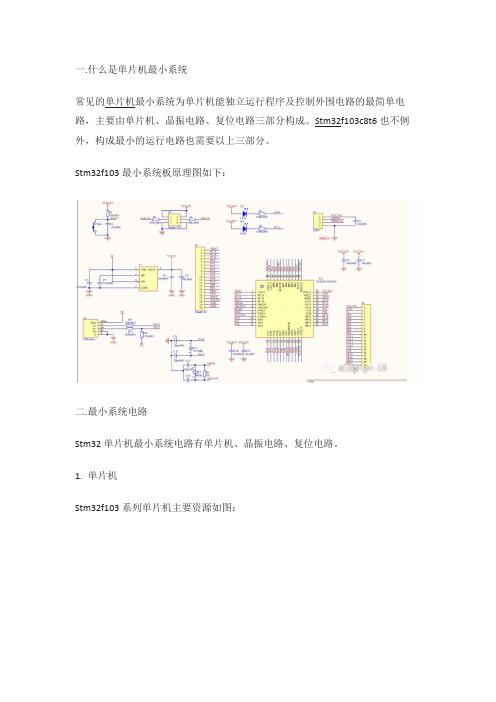
一.什么是单片机最小系统常见的单片机最小系统为单片机能独立运行程序及控制外围电路的最简单电路,主要由单片机、晶振电路、复位电路三部分构成。
Stm32f103c8t6也不例外,构成最小的运行电路也需要以上三部分。
Stm32f103最小系统板原理图如下:二.最小系统电路Stm32单片机最小系统电路有单片机、晶振电路、复位电路。
1. 单片机Stm32f103系列单片机主要资源如图:Stm32f103c8t6工作电压为2-3.6V(一般采用3.3V),内置64-128KBytes Flash,20KBytesSRAM,带有37个通用GPIO口(含特殊功能IO)。
在最小系统板上主要连接晶振电路、复位电路、工作电源、以及配置BOOT启动方式。
BOOT启动方式主要有三种,主闪存存储器启动、系统存储器启动、内置SRAM 启动,对应的BOOT引脚状态如下图:最常用的模式为主闪存存储器启动,即内部Flash启动,BOOT1=0,BOOT1=x(x 表示0或1均可)。
(注意三种模式的对应启动地址均不一样,内部Flash启动的地址为0x0800000)2. 晶振电路(1)主时钟晶振Stm32单片机内部自带一个8MHz的RC时钟,在符合设计需求的情况下,可通过程序在初始化时钟函数内,选择采用内部时钟。
外部主时钟晶振主要作为供单片机内核的时钟源,官方推荐晶振电路主要参数如下:Stm32单片机外部晶振为4-16MHz,常用8MHz,电路图如下:(2)RTC时钟晶振同样,RTC时钟在符合设计需求的情况下,可选用内部自带的40kHz RTC时钟。
外部晶振32.768KHz主要作为单片机内部RTC时钟的时钟源,电路图如下:3. 复位电路复位电路由RC电路及按键构成,10k电阻及1uF电容组成的RC电路;stm32单片机复位引脚为低电平有效,复位电路的作用是使单片机复位引脚在上电时,确保复位引脚至少有1ms以上的低电平状态。
复位按键的作用是当按键按下,复位引脚的被拉至低电平,单片机触发复位。
第三章STM32最小系统的设计
2、TTL与232电平转换电路 3、USB转串口转换电路
3. STM电源控制(PWR)
VDDA/VSSA独立电源/地 2.0至3.6V:为ADC、复位、 RC振荡器和PLL的模拟部分 供电。使用ADC时,VDD不 得小于2.4V。VREF+的电压 范围2.4V-VDDA, VREF-引 脚若有必须连接到VSSA。
应用程序代码 • SDRAM模块——为系统运行提供动态存储空间,是系
统代码运行的主要区域
1、引脚
引脚分类:
➢ 电源: (VBAT)、(VDD VSS)、(VDDA VSSA)、(VREF+ VREF-)等; ➢ 复位与启动:NRST、BOOT0、BOOT1 ➢ 晶振: 主晶振OSC_IN OSC_OUT、RTC晶振 ➢ 下载:JTMS_SWDIO、JTCK_SWCLK JTDI JTDO JNTRST等 ➢ GPIO: PA0-PA15等,专用器件接到专用的总线,比如I2C,SPI, SDIO,FSMC,DCMI这些总线的器件需要接到专用的IO
Power
JTAG UART
Flash SRAM
基于Cortex-M3的最小系统
• 时钟模块——通常经ARM内部锁相环进行相应的倍频, 以提供系统各模块运行所需的时钟频率输入
• 复位模块——实现对系统的复位 • 电源系统:为系统各模块供电 • 调试系统:
• JTAG模块——实现对程序代码的下载和调试 • UART模块——实现对调试信息的终端显示 • 存储系统: • Flash存储模块——存放启动代码、操作系统和用户
VDD:主电源/工作电压 VSS:地
2.0至3.6V:通过内置调压器 提供1.8V的电源,供内核使 用、3.3V供I/O管脚。 VBAT:后备电池供电
第2章-STM32单片机结构和最小系统

CRC
FLASH接口
RБайду номын сангаасC
DMA
USART1
SPI1 TIM1 ADC2 ADC1
PortE PortD PortC PortB PortA EXTI AFIO
PWR BKP
bxCAN USB/CAN SRAM
USB I2C2 I2C1
USART3 USART2
SPI2
IWDG WWDG
RTC
TIM4 TIM3 TIM2
通道5
DMA请求
2.2.1 系统总线构架
四个主动单元:Cortex-M3 内核的 ICode 总 线(I-bus)、DCode 总线(D-bus)、 System 总线(S-bus)和通用 DMA(GPDMA)。
三个被动单元:内部SRAM、内部Flash 存储 器、AHB 到 APB 的桥(AHB2APBx,连接 所有的 APB 设备)。
ADC2 GPIOD PWR SPI2/I2S
USART1 GPIOE BKP IWDG
SPI1 EXT1 CAN1 WWDG
TIM1 AFIO CAN2 RTC
GPIOA
I2C2 TIM7
GPIOB
I2C1 TIM6
UART5 TIM5
UART4 TIM4
USART3 TIM3
USART2 TIM2
PLLXTPRE /2
OSC32_IN OSC32_OUT
32.768KHz LSE OSC 低速外部时钟
40KHz LSI RC 低速内部时钟
/128 RTC
RTCCLK
RTCSEL[1:0]
LSI IWDGCLK
IWDG
USBCLK 45MHz
STM32F103C8T6中文资料_引脚图_最小系统

STM32F103C8T6中⽂资料_引脚图_最⼩系统Contents STM32F103x8,STM32F103xB Contents1Introduction (9)2Description (9)2.1Device overview (10)2.2Full compatibility throughout the family (13)2.3Overview (14)2.3.1ARM?Cortex?-M3core with embedded Flash and SRAM (14)2.3.2Embedded Flash memory (14)2.3.3CRC(cyclic redundancy check)calculation unit (14)2.3.4Embedded SRAM (14)2.3.5Nested vectored interrupt controller(NVIC) (14)2.3.6External interrupt/event controller(EXTI) (15)2.3.7Clocks and startup (15)2.3.8Boot modes (15)2.3.9Power supply schemes (15)2.3.10Power supply supervisor (15)2.3.11Voltage regulator (16)2.3.12Low-power modes (16)2.3.13DMA (17)2.3.14RTC(real-time clock)and backup registers (17)2.3.15Timers and watchdogs (17)2.3.16I2C bus (19)2.3.17Universal synchronous/asynchronous receiver transmitter(USART)..192.3.18Serial peripheral interface(SPI) (19)2.3.19Controller area network(CAN) (19)2.3.20Universal serial bus(USB) (19)2.3.21GPIOs(general-purpose inputs/outputs) (20)2.3.22ADC(analog-to-digital converter) (20)2.3.23T emperature sensor (20)2.3.24Serial wire JTAG debug port(SWJ-DP) (20)3Pinouts and pin description (21)4Memory mapping (34)2/105DocID13587Rev16STM32F103x8,STM32F103xB Contents5Electrical characteristics (35)5.1Parameter conditions (35)5.1.1Minimum and maximum values (35)5.1.2Typical values (35)5.1.3Typical curves (35)5.1.4Loading capacitor (35)5.1.5Pin input voltage (35)5.1.6Power supply scheme (36)5.1.7Current consumption measurement (37)5.2Absolute maximum ratings (37)5.3Operating conditions (38)5.3.1General operating conditions (38)5.3.2Operating conditions at power-up/power-down (39)5.3.3Embedded reset and power control block characteristics (40) 5.3.4Embedded reference voltage (41)5.3.5Supply current characteristics (41)5.3.6External clock source characteristics (51)5.3.7Internal clock source characteristics (55)5.3.8PLL characteristics (57)5.3.9Memory characteristics (57)5.3.10EMC characteristics (58)5.3.11Absolute maximum ratings(electrical sensitivity) (60)5.3.12I/O current injection characteristics (61)5.3.13I/O port characteristics (62)5.3.14NRST pin characteristics (68)5.3.15TIM timer characteristics (69)5.3.16Communications interfaces (70)5.3.17CAN(controller area network)interface (75)5.3.1812-bit ADC characteristics (76)5.3.19T emperature sensor characteristics (80)6Package characteristics (81)6.1Package mechanical data (81)6.2Thermal characteristics (93)6.2.1Reference document (93)6.2.2Selecting the product temperature range (94)DocID13587Rev163/105Contents STM32F103x8,STM32F103xB7Ordering information scheme (96)8Revision history (97)4/105DocID13587Rev16STM32F103x8,STM32F103xB List of tables List of tablesT able1.Device summary (1)T able2.STM32F103xx medium-density device features and peripheral counts (10)T able3.STM32F103xx family (13)T able4.Timer feature comparison (17)T able5.Medium-density STM32F103xx pin definitions (28)T able6.Voltage characteristics (37)T able7.Current characteristics (38)T able8.Thermal characteristics (38)T able9.General operating conditions (38)T able10.Operating conditions at power-up/power-down (39)T able11.Embedded reset and power control block characteristics (40)T able12.Embedded internal reference voltage (41)T able13.Maximum current consumption in Run mode,code with data processingrunning from Flash (42)T able14.Maximum current consumption in Run mode,code with data processingrunning from RAM (42)T able15.Maximum current consumption in Sleep mode,code running from Flash or RAM (44) T able16.Typical and maximum current consumptions in Stop and Standby modes (45)T able17.Typical current consumption in Run mode,code with data processingrunning from Flash (48)T able18.Typical current consumption in Sleep mode,code running from Flash orRAM (49)T able19.Peripheral current consumption (50)T able20.High-speed external user clock characteristics (51)T able21.Low-speed external user clock characteristics (51)T able22.HSE4-16MHz oscillator characteristics (53)T able23.LSE oscillator characteristics(f LSE=32.768kHz) (54)T able24.HSI oscillator characteristics (55)T able25.LSI oscillator characteristics (56)T able26.Low-power mode wakeup timings (57)T able27.PLL characteristics (57)T able28.Flash memory characteristics (57)T able29.Flash memory endurance and data retention (58)T able30.EMS characteristics (59)T able31.EMI characteristics (59)T able32.ESD absolute maximum ratings (60)T able33.Electrical sensitivities (60)T able34.I/O current injection susceptibility (61)T able35.I/O static characteristics (62)T able36.Output voltage characteristics (66)T able37.I/O AC characteristics (67)T able38.NRST pin characteristics (68)T able39.TIMx characteristics (69)T able40.I2C characteristics (70)T able41.SCL frequency(f PCLK1=36MHz.,V DD_I2C=3.3V) (71)T able42.SPI characteristics (72)T /doc/730a8438ac51f01dc281e53a580216fc710a531c.html B startup time (74)T /doc/730a8438ac51f01dc281e53a580216fc710a531c.html B DC electrical characteristics (75) DocID13587Rev165/105List of tables STM32F103x8,STM32F103xBT /doc/730a8438ac51f01dc281e53a580216fc710a531c.html B:Full-speed electrical characteristics (75) T able46.ADC characteristics (76)T able47.R AIN max for f ADC=14MHz (77)T able48.ADC accuracy-limited test conditions (77)T able49.ADC accuracy (78)T able50.TS characteristics (80)T able51.VFQFPN366x6mm,0.5mm pitch,package mechanical data (82)T able52.UFQFPN487x7mm,0.5mm pitch,package mechanical data (83)T able53.LFBGA100-10x10mm low profile fine pitch ball grid array packagemechanical data (85)T able54.LQPF100,14x14mm100-pin low-profile quad flat package mechanical data (87)T able55.UFBGA100-ultra fine pitch ball grid array,7x7mm,0.50mm pitch,packagemechanical data (88)T able56.LQFP64,10x10mm,64-pin low-profile quad flat package mechanical data (89)T able57.TFBGA64-8x8active ball array,5x5mm,0.5mm pitch,package mechanical data (90) T able58.LQFP48,7x7mm,48-pin low-profile quad flat package mechanical data (92)T able59.Package thermal characteristics (93)T able60.Ordering information scheme (96)T able61.Document revision history (97)6/105DocID13587Rev16STM32F103x8,STM32F103xB List of figures List of figuresFigure1.STM32F103xx performance line block diagram (11)Figure2.Clock tree (12)Figure3.STM32F103xx performance line LFBGA100ballout (21)Figure4.STM32F103xx performance line LQFP100pinout (22)Figure5.STM32F103xx performance line UFBGA100pinout (23)Figure6.STM32F103xx performance line LQFP64pinout (24)Figure7.STM32F103xx performance line TFBGA64ballout (25)Figure8.STM32F103xx performance line LQFP48pinout (26)Figure9.STM32F103xx performance line UFQFPN48pinout (26)Figure10.STM32F103xx performance line VFQFPN36pinout (27)Figure11.Memory map (34)Figure12.Pin loading conditions (36)Figure13.Pin input voltage (36)Figure14.Power supply scheme (36)Figure15.Current consumption measurement scheme (37)Figure16.Typical current consumption in Run mode versus frequency(at3.6V)-code with data processing running from RAM,peripherals enabled (43)Figure17.Typical current consumption in Run mode versus frequency(at3.6V)-code with data processing running from RAM,peripherals disabled (43)Figure18.Typical current consumption on V BAT with RTC on versus temperature at different V BAT values (45)Figure19.Typical current consumption in Stop mode with regulator in Run mode versus temperature at V DD=3.3V and3.6V (46)Figure20.Typical current consumption in Stop mode with regulator in Low-power mode versus temperature at V DD=3.3V and3.6V (46)Figure21.Typical current consumption in Standby mode versus temperature atV DD=3.3V and3.6V (47)Figure22.High-speed external clock source AC timing diagram (52)Figure23.Low-speed external clock source AC timing diagram (52)Figure24.Typical application with an8MHz crystal (53)Figure25.Typical application with a32.768kHz crystal (55)Figure26.Standard I/O input characteristics-CMOS port (64)Figure27.Standard I/O input characteristics-TTL port (64)Figure28.5V tolerant I/O input characteristics-CMOS port (65)Figure29.5V tolerant I/O input characteristics-TTL port (65)Figure30.I/O AC characteristics definition (68)Figure31.Recommended NRST pin protection (69)Figure32.I2C bus AC waveforms and measurement circuit (71)Figure33.SPI timing diagram-slave mode and CPHA=0 (73)Figure34.SPI timing diagram-slave mode and CPHA=1(1) (73)Figure35.SPI timing diagram-master mode(1) (74)/doc/730a8438ac51f01dc281e53a580216fc710a531c.html B timings:definition of data signal rise and fall time (75)Figure37.ADC accuracy characteristics (78)Figure38.Typical connection diagram using the ADC (79)Figure39.Power supply and reference decoupling(V REF+not connected to V DDA) (79)Figure40.Power supply and reference decoupling(V REF+connected to V DDA) (80)Figure41.VFQFPN366x6mm,0.5mm pitch,package outline(1) (82)Figure42.VFQFPN36recommended footprint(dimensions in mm)(1)(2) (82)DocID13587Rev167/105List of figures STM32F103x8,STM32F103xBFigure43.UFQFPN487x7mm,0.5mm pitch,package outline (83)Figure44.UFQFPN48recommended footprint (84)Figure45.LFBGA100-10x10mm low profile fine pitch ball grid array packageoutline (85)Figure46.Recommended PCB design rules(0.80/0.75mm pitch BGA) (86)Figure47.LQFP100,14x14mm100-pin low-profile quad flat package outline (87)Figure48.LQFP100recommended footprint(1) (87)Figure49.UFBGA100-ultra fine pitch ball grid array,7x7mm,0.50mm pitch,package outline (88)Figure50.LQFP64,10x10mm,64-pin low-profile quad flat package outline (89)Figure51.LQFP64recommended footprint(1) (89)Figure52.TFBGA64-8x8active ball array,5x5mm,0.5mm pitch,package outline (90)Figure53.Recommended PCB design rules for pads(0.5mm pitch BGA) (91)Figure54.LQFP48,7x7mm,48-pin low-profile quad flat package outline (92)Figure55.LQFP48recommended footprint(1) (92)Figure56.LQFP100P D max vs.T A (95)8/105DocID13587Rev16STM32F103x8,STM32F103xB Introduction 1IntroductionThis datasheet provides the ordering information and mechanical device characteristics ofthe STM32F103x8and STM32F103xB medium-density performance line microcontrollers.For more details on the whole STMicroelectronics STM32F103xx family,please refer toSection2.2:Full compatibility throughout the family.The medium-density STM32F103xx datasheet should be read in conjunction with the low-,medium-and high-density STM32F10xxx reference manual.The reference and Flash programming manuals are both available from theSTMicroelectronics website /doc/730a8438ac51f01dc281e53a580216fc710a531c.html .For information on the Cortex?-M3core please refer to the Cortex?-M3T echnicalReference Manual,available from the /doc/730a8438ac51f01dc281e53a580216fc710a531c.html website at the following address:/doc/730a8438ac51f01dc281e53a580216fc710a531c.html /help/index.jsp?topic=/com.arm.doc.ddi0337e/2DescriptionThe STM32F103xx medium-density performance line family incorporates the high-performance ARM Cortex?-M332-bit RISC core operating at a72MHz frequency,high-speed embedded memories(Flash memory up to128Kbytes and SRAM up to20Kbytes),and an extensive range of enhanced I/Os and peripherals connected to two APB buses.Alldevices offer two12-bit ADCs,three general purpose16-bit timers plus one PWM timer,aswell as standard and advanced communication interfaces:up to two I2Cs and SPIs,threeUSART s,an USB and a CAN.The devices operate from a2.0to3.6V power supply.They are available in both the–40to+85°C temperature range and the–40to+105°C extended temperature range.Acomprehensive set of power-saving mode allows the design of low-power applications.The STM32F103xx medium-density performance line family includes devices in six differentpackage types:from36pins to100pins.Depending on the device chosen,different sets ofperipherals are included,the description below gives an overview of the complete range ofperipherals proposed in this family.These features make the STM32F103xx medium-density performance line microcontrollerfamily suitable for a wide range of applications such as motor drives,application control,medical and handheld equipment,PC and gaming peripherals,GPS platforms,industrialapplications,PLCs,inverters,printers,scanners,alarm systems,video intercoms,and HVACs.DocID13587Rev169/105TimersCommunicationDescription STM32F103x8,STM32F103xB 2.1Device overviewTable2.STM32F103xx medium-density device features and peripheral1.On the TFBGA64package only15channels are available(one analog input pin has been replaced by‘Vref+’).10/105DocID13587Rev16Peripheral STM32F103Tx STM32F103Cx STM32F103Rx STM32F103Vx Flash-Kbytes64128641286412864128 SRAM-Kbytes20202020 General-purpose3333Advanced-control1111SPI12222I C1222USART2333USB1111CAN1111 GPIOs2637518012-bit synchronized ADCNumber of channels210channels210channels2(1)16channels216channels CPU frequency72MHzOperating voltage 2.0to3.6VOperating temperaturesAmbient temperatures:-40to+85°C/-40to+105°C(see Table9)Junction temperature:-40to+125°C(see Table9)Packages VFQFPN36LQFP48,UFQFPN48LQFP64,TFBGA64LQFP100,LFBGA100,UFBGA100f l a s ho b lI n t e r f a c eB u s M a t r i xA HB :F m a x =48/72M H zA PB 2:F m a x =48/72M H zA PB 1:F m a x =24/36M H zpbusPCLK2 HCLK CLOCK RTC AWUTAMPER -RTCSTM32F103x8, STM32F103xBDescriptionFigure 1. STM32F103xx performance line block diagram TRACECLKTRACED[0:3] as ASNJTRSTTRSTJTDIJTCK/SWCLK JTMS/SWDIOJTDO as AFTPIUTrace/trigSW/JTAGCortex -M3 CPUIbusF max : 7 2M Hz DbusTraceControlle rFlash 128 KB64 bitPOWERVOLT. REG. 3.3V TO 1.8V@VDDV DD = 2 to 3.6VV SSNVICSystemSRAM20 KB@VDDGP DMA7 channelsPCLK1 FCLKPLL &MANAGTXTAL OSC4-16 MHzOSC_INOSC_OUTRC 8 MHzNRST @VDDASUPPLYSUPERVISIONRC 40 kHz @VDDA@VBATIWDG Standby interfaceV BATVDDA VSSA 80AF PA[15:0] PB[15:0] POR / PDRPVDEXTIWAKEUPGPIOAGPIOBRstIntAHB2 AHB2APB2 APB1XTAL 32 kHzBackup reg Backu p i nterf ace TIM2 TIM3 OSC32_IN OSC32_OUT4 Channels 4 ChannelsPC[15:0]GPIOCTIM 44 ChannelsPD[15:0]GPIOD PE[15:0] GPIOEUSART2USART3RX,TX, CTS, RTS,CK, SmartCard as AFRX,TX, CTS, RTS, CK, SmartCard as AF 4 Channels3 compl. ChannelsETR and BKINMOSI,MISO, SCK,NSS as AFRX,TX, CTS, RTS,TIM1SPI12x(8x16bit)SPI2I2C1 I2C2MOSI,MISO,SCK,NSS as AFSCL,SDA,SMBA as AFSCL,SDA as AFSmartCard as AFUSART1@VDDAbxCANUSBDP/CAN_TXUSB 2.0 FSUSBDM/CAN_RX16AF V REF+ V REF -12bit ADC1 IF12bit ADC2 IFSRAM 512BWWDGTemp sensorai14390d1. T A = –40 °C to +105 °C (junction temperature up to 125 °C).2. AF = alternate function on I/O port pin.DocID13587 Rev 1611/105peripheralsIf (APB2 prescaler =1) x1 ADC /2, 4, 6, 8 ADCCLK DescriptionSTM32F103x8, STM32F103xBFigure 2. Clock treeFLITFCLKto Flash programming interface8 MHz HSI RCHSIUSBPrescaler 48 MHzUSBCLKto USB interface/2/1, 1.572 MHz maxClockHCLKto AHB bus, core, memory and DMA PLLSRCSWPLLMUL/8Enable (3 bits)to Cortex System timer..., x16 x2, x3, x4 PLLHSIPLLCLK HSESYSCLK72 MHz max AHB Prescaler /1, 2..512 APB1 Prescaler/1, 2, 4, 8, 16free running clock36 MHz max PCLK1to APB1Peripheral Clock Enable (13 bits)TIM2,3, 4to TIM2, 3and 4CSSIf (APB1 prescaler =1) x1 TIMXCLKelse x2 Peripheral ClockEnable (3 bits)OSC_OUTOSC_IN4-16 MHzHSE OSCPLLXTPRE/2APB2Prescaler/1, 2, 4, 8, 16TIM1 timer 72 MHz maxPeripheral ClockEnable (11 bits) PCLK2peripherals to APB2to TIM1 TIM1CLK else x2 Peripheral Clock OSC32_INOSC32_OUT32.768 kHz/128LSERTCCLKto RTCPrescaler Enable (1 bit) to ADCRTCSEL[1:0]LSI RCLSIto Independent Watchdog (IWDG)40 kHzIWDGCLKLegend:HSE = high -speed external clock signalHSI = high -speed internal clock signalMCOMainClock Output/2PLLCLKHSI LSI = low -speed internal clock signal LSE = low -speed external clock signalHSESYSCLKMCOai149031. When the HSI is used as a PLL clock input, the maximum system clock frequency that can be achieved is 64 MHz.2. For the USB function to be available, both HSE and PLL must be enabled, with USBCLK running at 48 MHz.3. To have an ADC conversion time of 1 µs, APB2 must be at 14 MHz, 28 MHz or 56 MHz.12/105DocID13587 Rev 16STM32F103x8, STM32F103xBDescription2.2 Full compatibility throughout the familyThe STM32F103xx is a complete family whose members are fully pin -to -pin, software and feature compatible. In the reference manual, the STM32F103x4 and STM32F103x6 are identified as low -density devices, the STM32F103x8 andSTM32F103xB are referred to as medium -density devices, and the STM32F103xC, STM32F103xD and STM32F103xE are referred to as high -density devices.Low - and high -density devices are an extension of the STM32F103x8/B devices, they are specified in the STM32F103x4/6 and STM32F103xC/D/E datasheets, respectively. Low - density devices feature lower Flash memory and RAM capacities, less timers and peripherals. High -density devices have higher Flash memory and RAM capacities, and additional peripherals like SDIO, FSMC, I 2S and DAC, while remaining fully compatible with the other members of the STM32F103xx family .The STM32F103x4, STM32F103x6, STM32F103xC, STM32F103xD and STM32F103xE are a drop -in replacement for STM32F103x8/B medium -density devices, allowing the user to try different memory densities and providing a greater degree of freedom during the development cycle.Moreover, the STM32F103xx performance line family is fully compatible with all existing STM32F101xx access line and STM32F102xx USB access line devices.1.For orderable part numbers that do not show the A internal code after the temperature range code (6 or 7),the reference datasheet for electrical characteristics is that of the STM32F103x8/B medium -density devices.DocID13587 Rev 16 13/105PinoutLow -density devicesMedium -density devices High -density devices 16 KB Flash 32 KB Flash (1) 64 KB Flash 128 KB Flash 256 KB Flash 384 KB Flash 512 KB Flash6 KB RAM 10 KB RAM 20 KB RAM 20 KB RAM 48 KB RAM 64 KB RAM 64 KB RAM144 5 × USART s 4 × 16-bit timers, 2 × basic timers2 3 × SPIs, 2 × I Ss, 2 × I2Cs USB, CAN, 2 × PWM timers 3 × ADCs, 2 × DACs, 1 × SDIOFSMC (100 and 144 pins) 100 3 × USART s 3 × 16-bit timers 2 2 × SPIs, 2 × I Cs, USB, CAN, 1 × PWM timer2 × ADCs 64 2 × USART s 2 × 16-bit timers 2 1 × SPI, 1 × I C, USB, CAN, 1 × PWM timer 2 × ADCs 48 36Description STM32F103x8,STM32F103xB 2.3Overview2.3.1ARM?Cortex?-M3core with embedded Flash and SRAMThe ARM Cortex?-M3processor is the latest generation of ARM processors for embeddedsystems.It has been developed to provide a low-cost platform that meets the needs of MCUimplementation,with a reduced pin count and low-power consumption,while deliveringoutstanding computational performance and an advanced system response to interrupts.The ARM Cortex?-M332-bit RISC processor features exceptional code-efficiency,delivering the high-performance expected from an ARM core in the memory size usuallyassociated with8-and16-bit devices.The STM32F103xx performance line family having an embedded ARM core,is thereforecompatible with all ARM tools and software.Figure1shows the general block diagram of the device family.2.3.2Embedded Flash memory64or128Kbytes of embedded Flash is available for storing programs and data.2.3.3CRC(cyclic redundancy check)calculation unitThe CRC(cyclic redundancy check)calculation unit is used to get a CRC code from a32-bitdata word and a fixed generator polynomial.Among other applications,CRC-based techniques are used to verify data transmission orstorage integrity.In the scope of the EN/IEC60335-1standard,they offer a means ofverifying the Flash memory integrity.The CRC calculation unit helps compute a signature ofthe software during runtime,to be compared with a reference signature generated at link-time and stored at a given memory location.2.3.4Embedded SRAMTwenty Kbytes of embedded SRAM accessed(read/write)at CPU clock speed with0waitstates.2.3.5Nested vectored interrupt controller(NVIC)The STM32F103xx performance line embeds a nested vectored interrupt controller able tohandle up to43maskable interrupt channels(not including the16interrupt lines ofCortex?-M3)and16priority levels.Closely coupled NVIC gives low-latency interrupt processingInterrupt entry vector table address passed directly to the coreClosely coupled NVIC core interfaceAllows early processing of interruptsProcessing of late arriving higher priority interruptsSupport for tail-chainingProcessor state automatically savedInterrupt entry restored on interrupt exit with no instruction overhead14/105DocID13587Rev16万联芯城专注电⼦元器件配单服务,只售原装现货库存,万联芯城电⼦元器件全国供应,专为终端⽣产,研发企业提供现货物料,价格优势明显,BOM配单采购可节省逐个搜索购买环节,只需提交BOM物料清单,商城即可为您报价,解决客户采购烦恼,为客户节省采购成本,点击进⼊万联芯城。
