BD682中文资料
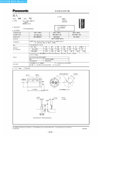
ECEC1HA682CJ中文资料(panasonic)中文数据手册「EasyDatasheet - 矽搜」
200
25 40 3.1 0.55 ECEC1AA273CJ
200
30 30 3.1 0.55 ECEC1AA273DJ
200
10
35 25 3.1 0.55 ECEC1AA273EJ
200
33000 25 45 3.4 0.55 ECEC1AA333CJ
200
30 35 3.4 0.55 ECEC1AA333DJ
100
1800 22 25 1.5 0.25 ECEC1HA182BJ
200
30 25 2.9 0.45 ECEC1CA123DJ
200
15000 22 40 3.2 0.45 ECEC1CA153BJ
200
25 35 3.2 0.45 ECEC1CA153CJ
200
16
30 30 3.2 0.45 ECEC1CA153DJ
200
18000 22 45 3.5 0.45 ECEC1CA183BJ
铝电解电容器/ HA
n 标准产品
W.V. (V)
Cap. (±20%)
(µF) 10000
外壳尺寸
产品规格
Dia. (mm)
长短
涟 当前
tan
(120Hz) (120Hz)
(mm)
(+105°C) (A)
(+20°C)
22 25 1.8 0.55
型号
PET套
码头长度
4.0mm
(无P.V.C.plate)
200
33000 30 45 4.7 0.45 ECEC1CA333DJ
100
35 35 4.7 0.45 ECEC1CA333EJ
100
BD683资料
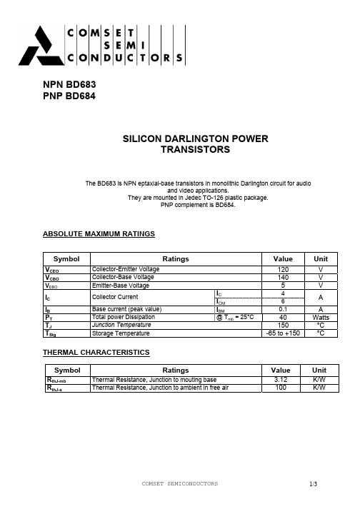
NPN BD683 PNP BD684SILICON DARLINGTON POWER TRANSISTORSThe BD683 is NPN eptaxial-base transistors in monolithic Darlington circuit for audio and video applications. They are mounted in Jedec TO-126 plastic package. PNP complement is BD684.ABSOLUTE MAXIMUM RATINGS SymbolVCEO VCBOVEBO Collector-Emitter Voltage Collector-Base Voltage Emitter-Base Voltage Collector Current Base current (peak value) Total power Dissipation Junction Temperature Storage TemperatureRatingsValue120 140 5 IC ICM IBM@ Tmb = 25°C 4 6 0.1UnitV V V A A Watts °C °CIC IB PT TJ TStg40 150 -65 to +150THERMAL CHARACTERISTICS SymbolRthJ-mb RthJ-aRatingsThermal Resistance, Junction to mouting base Thermal Resistance, Junction to ambient in free airValue3.12 100UnitK/W K/WCOMSET SEMICONDUCTORS1/3NPN BD683 PNP BD684ELECTRICAL CHARACTERISTICSTC=25°C unless otherwise notedSymbolICBO ICEO IEBO VCE(SAT) hFE VBE hfe fhfe VF I(SB) ton toffRatingsCollector cut-off current Collector cut-off current Emitter cut-offcurrent Collector-Emitter saturation Voltage DC Current GainTest Condition(s)IE=0 , VCB= VCEOMAX=120 V IE=0 , VCB= 1/2VCBOMAX= 70V,Tj= 150°C IB=0 , VCE= 1/2VCEOMAX=60 V IC=0, VEB=5 V IC=1.5 A, IB=6 mAMin Typ750 10 0,8 2200 1500 60 0,8 4,5Max0,2 1 0,2 5 2,5 2,5 2 8UnitmA mA mA VVCE=3 V, IC=500 mA VCE=3 V, IC=1,5 A VCE=3 V, IC=4 A VCE=3 V, IC=1,5 A Base-Emitter Voltage(1&2) VCE=3 V, IC=1,5 A, f= 1 MHz Small signal current gain VCE=3 V, IC=1,5 A Ut-off frequency IF=1,5 A Diode forward voltage Second-breakdown collector VCE=50 V, tP= 20ms,non rep., without heatsink currentV kHz A µsTurn-on time Icon= 1,5A, Ibon= -Iboff= 6mA, VCC=30V Turn-off time 1. Measured under pulse conditions :tP <300µs, δ <2%. 2. VBE decreases by about 3,6 mV/K with increasing temperature.MECHANICAL DATA CASE TO-126DIMENSIONS mm A B C D E F G H L M N P min max 7.4 7.8 10.5 10.8 2.4 2.7 0.7 0.9 2.2 typ. 0.49 0.75 4.4 typ. 2.54 typ. 15.7 typ. 1.2 typ. 3.8 typ. 3.0 3.2 Pin 1 : Pin 2 : Pin 3 : inches min max 0.295 0.307 0.413 0.425 0.094 0.106 0.027 0.035 0.087 typ. 0.019 0.029 0.173 typ. 0.100 typ. 0.618 typ. 0.047 typ. 0.149 typ. 0.118 0.126 Emitter Collector BaseCOMSET SEMICONDUCTORS2/3Information furnished is believed to be accurate and reliable. However, CS assumes no responsability for the consequences of use of such information nor for errors that could appear.Data are subject to change without notice.COMSET SEMICONDUCTORS3/3。
DN68资料
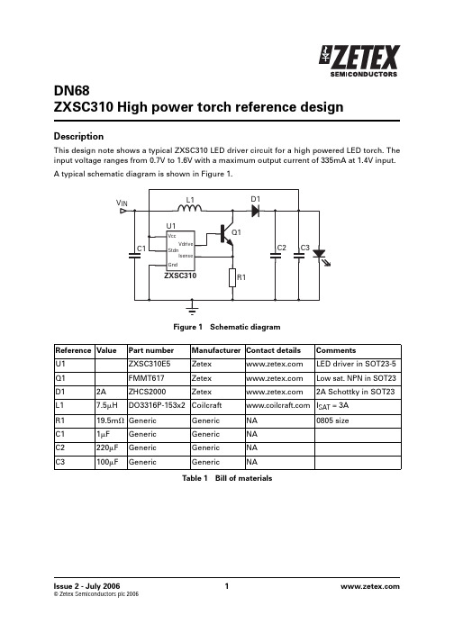
Issue 2 - July 2006© Zetex Semiconductors plc 2006DN68ZXSC310 High power torch reference designDescriptionThis design note shows a typical ZXSC310 LED driver circuit for a high powered LED torch. The input voltage ranges from 0.7V to 1.6V with a maximum output current of 335mA at 1.4V input.A typical schematic diagram is shown in Figure 1.Figure 1Schematic diagramReference Value Part number Manufacturer Contact details CommentsU1ZXSC310E5Zetex LED driver in SOT23-5Q1FMMT617Zetex Low sat. NPN in SOT23D12A ZHCS2000Zetex2A Schottky in SOT23L17.5HDO3316P-153x2Coilcraft I SAT = 3A R119.5m ⍀Generic Generic NA 0805 sizeC11F Generic Generic NA C2220F Generic Generic NA C3100FGenericGeneric NATable 1Bill of materials元器件交易网DN68 2Issue 2 - July 2006© Zetex Semiconductors plc 2006For international sales offices visit /officesZetex products are distributed worldwide. For details, see /salesnetworkThis publication is issued to provide outline information only which (unless agreed by the company in writing) may not be used, applied or reproduced for any purpose or form part of any order or contact or be regarded as a representation relating to the products or services concerned.The company reserves the right to alter without notice the specification, design, price or conditions of supply of any product or service.EuropeZetex GmbHStreitfeldstraße 19D-81673 München GermanyTelefon: (49) 89 45 49 49 0Fax: (49) 89 45 49 49 49europe.sales@AmericasZetex Inc700 Veterans Memorial Highway Hauppauge, NY 11788USATelephone: (1) 631 360 2222Fax: (1) 631 360 8222usa.sales@Asia PacificZetex (Asia Ltd)3701-04 Metroplaza Tower 1Hing Fong Road, Kwai Fong Hong KongTelephone: (852) 26100 611Fax: (852) 24250 494asia.sales@Corporate HeadquartersZetex Semiconductors plcZetex Technology Park, Chadderton Oldham, OL9 9LL United KingdomTelephone: (44) 161 622 4444Fax: (44) 161 622 4446hq@Figure 2Performance graphs。
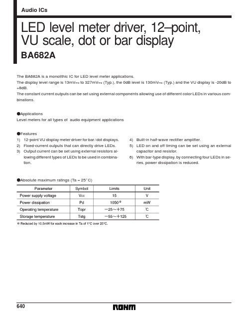
BA682A中文资料
FOperation notes (1) LED connection Connect the LEDs as indicated in Fig. 2. Note that the connection methods are different for bar and dot displays, and that in the case of bar display, pin 18 is open, while for dot display, pin 18 is connected to GND. When using different color LEDs that have different current values (e.g. green for the lower 10 LEDs and red for the top two) set the value of the current to the larger LED current using the external resistor, and adjust the current value for LEDs that require a smaller current by connecting resistors in parallel them. If you wish to remove LEDs, do so from the lowest level. (except when the 12th LED is not used for display alignment). Be certain to short unused LEDs. (2) LED current adjustment The LED current is set using R1. The relationship between the value of R1 and the typical LED current is given in Fig. 3.
FDMF6820A;中文规格书,Datasheet资料
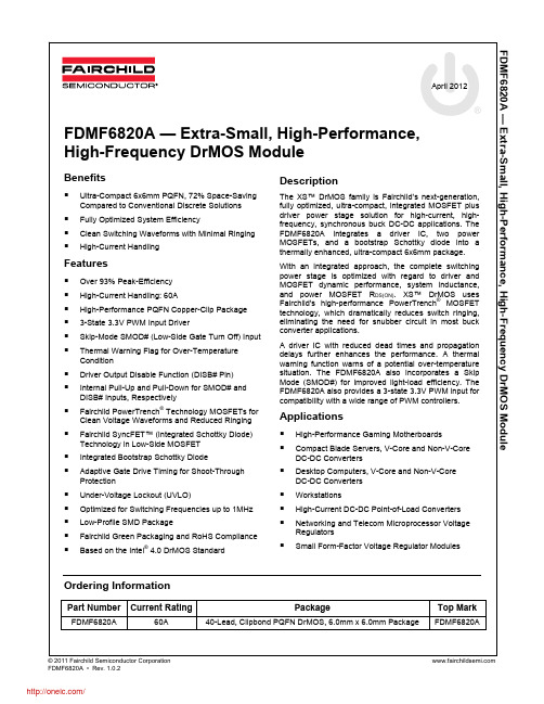
PHASE Switch node pin for bootstrap capacitor routing. Electrically shorted to VSWH pin. NC VIN
Switch node input. Provides return for high-side bootstrapped driver and acts as a sense point VSWH for the adaptive shoot-through protection. PGND GL THWN# DISB# PWM Power ground. Output stage ground. Source pin of the low-side MOSFET. For manufacturing test only. This pin must float; it must not be connected to any pin. Thermal warning flag, open collector output. When temperature exceeds the trip limit, the output is pulled LOW. THWN# does not disable the module. Output disable. When LOW, this pin disables the power MOSFET switching (GH and GL are held LOW). This pin has a 10µA internal pull-down current source. Do not add a noise filter capacitor. PWM signal input. This pin accepts a three-state 3.3V PWM signal from the controller.
常用三极管中文资料大全
品名/ 极性/ 管脚/功能/ 参数D718 NPN 30 音频功放开关120V8A80W /B668D774 NPN 39B 通用100V1A1W /B734D789 NPN 21 音频输出100V1A0.9WD820 NPN 12 彩行1500V5A50WD870 NPN 12 彩行1500V5A50W RRRRD880 NPN 28 音频功放开关60V3A10WD882 NPN 29 音频功放开关40V3A30WD884 NPN 28 音频功放开关330V7A40WD898 NPN 12 彩行1500V3A50WD951 NPN 12 彩行1500V3A65WD965 NPN 21 音频40V5A0.75WD966 NPN 21 音频40V5A1WD985 NPN 29 功放150V1.5A10WD986 NPN 29 功放150V1.5A10WD1025 NPN 28 达林顿功放200V8A50WD1037 NPN BCE 音频功放开关150V30A180WD1047 NPN 30 音频功放开关160V12A100W /B817D1071 NPN 28 功放300V6A40W DRA-LD1163A NPN 28 行偏转用350V7A40W60MHzD1175 NPN 12 行偏转用1500V5A100W β=15 原D1273 NPN 28 音频功放80V3A40W50MHZβ=1500D1302 NPN 21 音频25V0.5A0.5W200MHZD1397 NPN BCE 开关1500V3.5A50W3MHzD1398 NPN BCE 开关1500V5A50W3MHzD1403 NPN 28B 彩行1500V6A120WD1403 NPN 28B 彩行1500V6A120W 原D1415 NPN 28B 功放电源开关100V7A40Wβ=6000达林顿D1416 NPN 28B 功放电源开关80V7A40Wβ=6000(达林顿) D1426 NPN 28B 彩行1500V3.5A80Wβ=12 RRRRRD1427 NPN 28B 彩行1500V5A80Wβ=12 RRRRRD1428 NPN 28B 彩行1500V6A80Wβ=12 RRRRD1431 NPN 28B 彩行1500V5A80Wβ=20D1433 NPN 28B 彩行1500V7A80Wβ=20D1439 NPN BCE 彩行1500V3A80Wβ=8D1541 NPN 28B 彩行1500V3A80Wβ=20D1545 NPN 28B 彩行1500V5A50Wβ=20D1547 NPN BCE 彩行1500V7A80Wβ=20D1554 NPN BCE 彩行1500V3.5A80Wβ=12D1555 NPN BCE 彩行1500V5A80Wβ=12D1556 NPN BCE 彩行1500V6A80Wβ=12D1559 NPN BCE 达林顿功放100V20A100Wβ=5000/B1079 D1590 NPN 28 达林顿功放150V8A25W β=15000D1632 NPN 28B 彩行1500V4A70WD1640 NPN 29 达林顿功放120V2A1.2W β=4000-40000 D1651 NPN SP 彩行1500V5A60W3MHZD1710 NPN BCE 彩行1500V5A50WD1718 NPN 28C 音频功放180V15A3.5W20MHZD1762 NPN BCE 音频功放开关60V3A25W90MHZ /B1185 D1843 NPN BCE 低噪放大50V1A1WD1849 NPN 50A 彩行1500V7A120WD1850 NPN 50A 彩行1500V7A120WD1859 NPN 50A 音频80V0.7A1W120MHZD1863 NPN 50A 音频120V1A1W100MHZD1877 NPN 30 彩行1500V4A50W(带阻尼)D1879 NPN 30 彩行1500V6A60W(带阻尼)D1887 NPN 30 彩行1500V10A70WD1930 NPN 21 达林顿达林顿100V2A1.2Wβ=1000D1975 NPN 53A 音频功放180V15A150W COP:B1317D1978 NPN 21 达林顿120V1.5A0.9Wβ=30000D1980 NPN 61B 达林顿100V2A10Wβ=1000-10000D1981 NPN ECB 达林顿100V2A1WD1993 NPN 45B 音频低噪55V0.1A0.4WD1994A NPN ECB 音频驱动60V1A1WD1997 NPN 45B 激励管40V3A1.5W100MHZD2008 NPN ECB 音频功放80V1A1.2WD2012 NPN BCE 音频功放60V3A2W3MHZD2136 NPN ECB 功放80V1A1.2WD2155 NPN 53A 音频功放180V15A150WD2256 NPN 46 达林顿功放120V25A125Wβ=2000-20000 D2334 NPN 28B 彩行1500V5A80WD2335 NPN BCE 彩行1500V7A100WD2349 NPN BCE 大屏彩显行管D2374 NPN BCED2375 NPN BCED2388 NPN EBC 达林顿90V3A1.2WD2445 NPN BCE 彩行1500V12.5A120WD2498 NPN BCE 彩行1500V6A50WD2588 NPN BCE 点火器用DK55 NPN BEC 开关400V4A60WBC307 PNP 21a 通用50V0.2A0.3WBC327 PNP CBE 低噪音频50V0.8A0.625W COM BC337 BC337 NPN 21a 音频激励低噪50V0.8A0.625W COM BC327 BC338 NPN 21a 通用激励50V0.8A0.6BC546 NPN 21a 通用80V0.2A0.5WBC547 NPN CBE 通用50V0.2A0.5W300MHZBD135 NPN 29 音频功放45V1.5A12.5WBD136 PNP 29 音频功放45V1.5A12.5WBD137 NPN 29 音频功放60V1.5A12.5WBD138 PNP 29 音频功放60V1.5A12.5WBD139 PNP 29 音频功放80V1.5A12.5WBD237 NPN 29 音频功放100V2A25WBD238 PNP 29 音频功放100V2A25WBD243 NPN 28 音频功放45V6A65WBD244 PNP 28 音频功放45V6A65WBD681 NPN 29 达林顿功放100V4A40WBD682 NPN 29 达林顿功放100V4A40WBF458 NPN 29 视放250V0.1A10WBU208A NPN 12 彩行1500V5A12.5WBU208D NPN 12 彩行1500V5A12.5W (带阻尼)BU323 NPN 28 达林顿功放450V10A125WBU406 NPN 28 行管400V7A60WBU508A NPN 28 行管1500V7.5A75WBU508A NPN 28 行管1500V7.5A75W 原BU508D NPN 28 行管1500V7.5A75W (带阻尼)BU806 NPN 28 功放400V8A60W DAR-LBU932R NPN 12 功放500V15A150W DAR-LBU941 NPN 12BU1508DX NPN 28 开关功放BU2506DX NPN 30 开关功放1500V7A50W /600NSBU2508AF NPN 30 开关功放700V8A125W /600NSBU2508AX NPN 30 开关功放700V8A125W /600NSBU2508DF NPN 30 开关功放700V8A125W/600NS(带阻尼) BU2508DX NPN 30 开关功放1500V8A50W/600NS(带阻尼) BU2520AF NPN 30 开关功放800V10A150W 1/500NSBU2520AX NPN 30 开关功放1500V10A150W 1/500NSBU2520DF NPN 30 开关功放800V10A150W1/500NS(带阻) BU2520DX NPN 30 开关功放1500V10A50W/600NS (带阻) BU2522AF NPN 30 开关功放1500V11A150W /350NSBU2522AX NPN 30 开关功放1500V11A150W /350NSBU2525AF NPN 30 开关功放1500V12A150W /350NSBU2525AX NPN 30 开关功放1500V12A150W /350NSBU2527AF NPN 30 开关功放1500V15A150WBU2532AW NPN 30 开关功放1500V15A150W(大屏) BUH515 NPN BCE 行管1500V10A80WBUH515D NPN BCE 行管1500V10A80W(带阻尼)BUS13A NPN 12 开关功放1000V15A175WBUS14A NPN 12 开关功放1000V30A250WBUT11A NPN 28 开关功放1000V5A100WBUT12A NPN 28 开关功放450V10A125WBUV26 NPN 28 音频功放开关90V14A65W /250nsBUV28A NPN 28 音频功放开关225V10A65W /250nsBUV48A NPN 30 音频功放开关450V15A150WBUW13A NPN 30 功放开关1000V15A150WBUX48 NPN 12 功放开关850V15A125WBUX84 NPN 30 功放开关800V2A40WBUX98A NPN 12 功放开关400V30A210W5MHZDTA114 PNP 10K-10K 160V0.6A0.625W(带阻)DTC143 NPN 录像机用4.7K-4.7KHPA100 NPN BCE 大屏彩显行管21#HPA150 NPN BCE 大屏彩显行管21#HSE830 PNP BCE 音频功放80V115W1MHZHSE838 NPN BCE 音频功放80V115W1MHZ COP/MJ4502MN650 NPN BCE 行管1500V6A80WMJ802 NPN 12 音频功放开关90V30A200WMJ2955 PNP 12 音频功放开关60V15A115WMJ3055 NPN 12 音频功放开关60V15A115WMJ4502 PNP 12 音频功放开关90V30A200W COP/MJ802MJ10012 NPN 12 达林顿400V10A175WMJ10015 NPN 12 电源开关400V50A200WMJ10016 NPN 12 电源开关500V50A200WMJ10025 12 电源开关850V20A250WMJ11032 NPN 12 电源开关120V50A300W DAR-LMJ11033 PNP 12 电源开关120V50A300W DAR-LMJ13333 NPN 12 电源开关400V20A175WMJ15024 NPN 12 音频功放开关400V16A250W4MHZ(原25.00) MJ15025 PNP 12 音频功放开关400V16A250W4MHZ(原25.00) MJE271 PNP 29 达林顿MJE340 NPN 29 视放300V0.5A20WMJE350 PNP 29 视放300V0.5A20WMJE2955T PNP BCE 音频功放开关60V1075W2MHZMJE3055T NPN BCE 音频功放开关70V1075W2MHZMJE5822 PNP BCE 音频功放开关500V8AMJE9730 NPN BCEMJE13003 NPN 29 功放开关400V1.5A14WMJE13005 NPN 28 功放开关400V4A60WMJE13007 NPN 28 功放开关1500V2.5A60WBU2525AF NPN 30 开关功放1500V12A150W /350NSFBU2525AX NPN 30 开关功放1500V12A150W /350NSBU2527AF NPN 30 开关功放1500V15A150WZBU2532AW NPN 30 开关功放1500V15A150W(大屏)BUH515 NPN BCE 行管1500V10A80W;BUH515D NPN BCE 行管1500V10A80W(带阻尼)BUS13A NPN 12 开关功放1000V15A175W.BUS14A NPN 12 开关功放1000V30A250WBUT11A NPN 28 开关功放1000V5A100WBUT12A NPN 28 开关功放450V10A125WBUV26 NPN 28 音频功放开关90V14A65W /250nsBUV28A NPN 28 音频功放开关225V10A65W /250ns BUV48A NPN 30 音频功放开关450V15A150WBUW13A NPN 30 功放开关1000V15A150WBUX48 NPN 12 功放开关850V15A125WBUX84 NPN 30 功放开关800V2A40WBUX98A NPN 12 功放开关400V30A210W5MHZDTA114 PNP 10K-10K 160V0.6A0.625W(带阻)DTC143 NPN 录像机用4.7K-4.7KHPA100 NPN BCE 大屏彩显行管21#HPA150 NPN BCE 大屏彩显行管21#HSE830 PNP BCE 音频功放80V115W1MHZHSE838 NPN BCE 音频功放80V115W1MHZ COP/MJ4502 MMN650 NPN BCE 行管1500V6A80WMJ802 NPN 12 音频功放开关90V30A200WMJ2955 PNP 12 音频功放开关60V15A115W!MJ3055 NPN 12 音频功放开关60V15A115WMJ4502 PNP 12 音频功放开关90V30A200WMJ10012 NPN 12 达林顿400V10A175WMJ10015 NPN 12 电源开关400V50A200WMJ10016 NPN 12 电源开关500V50A200WMJ10025 12 电源开关850V20A250WMJ11032 NPN 12 电源开关120V50A300WMJ11033 PNP 12 电源开关120V50A300WMJ13333 NPN 12 电源开关400V20A175WMJ15024 NPN 12 音频功放开关400V16A250W4MHZ MJ15025 PNP 12 音频功放开关400V16A250W4MHZ MJE271 PNP 29 达林顿MJE340 NPN 29 视放300V0.5A20WMJE350 PNP 29 视放300V0.5A20WMJE2955T PNP BCE 音频功放开关60V1075W2MHZ MJE3055T NPN BCE 音频功放开关70V1075W2MHZ MJE5822 PNP BCE 音频功放开关500V8AMJE9730 NPN BCEMJE13003 NPN 29 功放开关400V1.5A14WMJE13005 NPN 28 功放开关400V4A60WMJE13007 NPN 28 功放开关1500V2.5A60WTIP31C NPN BCE 功放开关100V3A40W3MHZTIP32C PNP BCE 功放开关100V3A40W3MHZTIP35C NPN 30 音频功放开关100V25A125W3MHZTIP36C PNP 30 音频功放开关100V25A125W3MHZTIP41C NPN 30 音频功放开关100V6A65W3MHZTIP42C PNP 30 音频功放开关100V6A65W3MHZTIP102 NPN 28 音频功放开关100V8A2WTIP105 28 音频功放开关9 WTIP122 NPN 28 音频功放开关100V8A65W DARLTIP127 PNP 28 音频功放开关100V8A65W DARLTIP137 PNP 28 音频功放开关100V8A70W DARLTIP142 NPN 30 音频功放开关100V10A125W DAR-L TIP142大NPN 30 音频功放开关100V10A125WTIP147 PNP 30 音频功放开关100V10A125WTIP147大PNP 30 音频功放开关100V10A125WTIP152 电梯用TL431 21 电压基准源UGN3120 SGO 霍尔开关UGN3144 SGO 霍尔开关60MIAL1 电磁/微波炉1000V60A300WT30G40 NPN BCE 大功率开关管400V30A300W MPSA42 NPN 21E 电话视频放大300V0.5A0.625W MPSA92 PNP 21E 电话视频放大300V0.5A0.625W MPS2222A NPN 21 高频放大75V0.6A0.625W300MHZ 9011 NPN EBC 高频放大50V30mA0.4W150MHz9012 PNP 贴片低频放大50V0.5A0.625W9013 NPN EBC 低频放大50V0.5A0.625W9013 NPN 贴片低频放大50V0.5A0.625Wc9014 NPN EBC 低噪放大50V0.1A0.4W150MHZx9015 PNP EBC 低噪放大50V0.1A0.4W150MHZs9018 NPN EBC 高频放大30V50MA0.4W1GHZH8050 NPN EBC 高频放大40V1.5A1W100MHZ8550 PNP EBC 高频放大40V1.5A1W100MHZ2N2222 NPN 4A 高频放大60V0.8A0.5W25/200NSβ=45 2N2222A NPN 小铁高频放大75V0.6A0.625W300MHZ 2N2369 NPN 4A 开关40V0.5A0.3W800MHZ2N2907 NPN 4A 通用60V0.6A0.4W26/70NSβ=200K2N3055 NPN 12 功率放大100V15A115Ws2N3440 NPN 6 视放开关450V1A1W15MHZ2N3773 NPN 12 音频功放开关160V16A150W2N3904 NPN 21E 通用60V0.2Aβ=100-4002N3906 PNP 21E 通用40V0.2Aβ=100-400u2N5401 PNP 21E 视频放大160V0.6A0.625W100MHZ k2N5551 NPN 21E 视频放大160V0.6A0.625W100MHZ Y2N5685 NPN 12 音频功放开关60V50A300W2N6277 NPN 12 功放开关180V50A250W2N6609 PNP 12 音频功放开关160V15A150Wu2N6678 NPN 12 音频功放开关650V15A175W15MHZ 2N6718 NPN 小铁音频功放开关100V2A2W50MHZ3DA87A NPN 6 视频放大100V0.1A1W3DG6A NPN 6 通用15V20mA0.1W100MHz3DG6B NPN 6 通用20V20mA0.1W150MHz3DG6C NPN 6 通用20V20mA0.1W250MHz3DG6D NPN 6 通用30V20mA0.1W150MHzl3DG12C NPN 7 通用45V0.3A0.7W200MHz3DK2B NPN 7 开关30V30mA0.2W3DK4B NPN 7 开关40V0.8A0.7W3DK7C NPN 7 开关25V50mA0.3W3DD15D NPN 12 电源开关300V5A50W3DD102C NPN 12 电源开关300V5A50W3522V 5.2V稳压管录像机用HA634 PNP 28E 音频功放开关40V2A10WA708 PNP 6 NF/S 80V0.7A0.8WA715C PNP 29 音频功放开关35V2.5A10W160MHZfA733 PNP 21 通用50V0.1A180MHZRA741 PNP 4 S 20V0.1A <70/120nSA781 PNP 39B 开关20V0.2A <80/160NSA928 PNP ECB 通用20V1A0.25WA933 PNP 21 Uni 50V0.1A140MHzA940 PNP 28 音频功放开关150V1.5A25W4MHZA950 PNP 21 通用30V0.8A0.6WA966 PNP 21 音频激励输出30V1.5A0.9WA968 PNP 28 音频功放开关160V1.5A25W100MHZA1009 PNP BCE 功放开关350V2A15WA1012 PNP 28 音频功率放60V5A25WA1013 PNP 21 视频放大160V1A0.9WA1015 PNP 21 通用60V0.15A0.4W8MHZA1020 PNP 21 音频开关50V2A0.9WA1123 PNP 21 低噪放大150V0.05A0.75WNA1162 PNP 21d 通用贴片50V0.15A0.15WFA1216 PNP BCE 功放开关180V17A200W20MHZA1220 PNP 29 音频功放开关120V1.5A20W150MHZ/C2690 A1265 PNP BCE 功放开关140V10A100W30MHZ /C3182 A1295 PNP BCE 功放开关230V17A200W30MHZ /C3264 A1301 PNP BCE 功放开关160V10A100W30MHZ /C3280 A1302 PNP BCE 功放开关200V15A150W30MHZ /C32814 A1358 ? PNP 高频120V1A10W120MHZA1444 PNP BCE 高速电源开关100V15A30W80MHZA1494 PNP BCE 功放开关200V17A200W20MHZ /C3858 A1516 PNP BCE 功放开关180V12A130W25MHZA1668 PNP 28B 电源开关200V2A25W20MHZTA1785 PNP BCE 驱动400V1A1W/120V1A0.9W140MHA1941 PNP BCE 功放开关140V10A100WCOP:5198A1943 PNP BCE 功放开关230V15A150WA1988 PNP 30 功放开关B449 PNP 12 功放开关50V3.5A22.5W 锗管B631K PNP 29 音频功放开关120V1A8W130MHZ /D600K8 B647 PNP 21 通用120V1A0.9W140MHZ /D667B649 PNP 29 视放180V1.5A1W /D669B669 PNP 28 达林顿功放70V4A40WB673 PNP 28 达林顿功放100V7A40WB675 PNP 28 达林顿功放60V7A40WB688 PNP BCE 音频功放开关120V8A80WB734 PNP 39B 通用60V1A1WB744 PNP 21 通用30V0.1A0.25WB772 PNP 29 音频功放开关40V3A10WB774 PNP 21 通用30V0.1A0.25WB817 PNP 30 功放开关160V12A100W /D1047B834 PNP 28 功放开关60V3A30WB937A PNP 功放开关60V2A35 WB1020 PNP 28 功放开关达林顿100V7A40Wβ=6000B1079 PNP 30 达林顿功放100V20A100Wβ=5000/D1559 B1185 PNP 28B 功放开关60V3A25W 70MHZ /D1762B1238 PNP ECB 功放开关80V0.7A1W 100MHZB1240 PNP 39B 功放开关40V2A1W100HZB1243 PNP 39B 功放开关40V3A1W70HZB1316 PNP 54B 驱动功放达林顿100V2A10Wβ=15000 B1317 PNP BCE 音频功放180V15A150WB1335 PNP 28 音频功放低噪80V4A30W 12MHZB1375 PNP BCE 音频功放60V3A2W9MHZB1400 PNP 28B 达林顿功放120V6A25W β=1000-20000 B1429 PNP BCE 功放开关180V15A150WB1494 PNP BCE 达林顿功放120V25A120Wβ=2000-20000 C106 NPN EBC 音频功放开关60V1.5A15WC380 NPN 21 高频放大35V0.03A250MHZC458 NPN 21 通用30V0.1A230MHzC536 NPN 21 通用40V0.1A180MHZC752 NPN 21 通用30V0.1A300MHzC815 NPN 21 通用60V0.2A0.25WC828 NPN 21 通用45V0.05A0.25WC900 NPN 21 低噪放大30V0.03A100MHZC943 NPN 4A 通用60V0.2A200MHZC945 NPN 21 通用50V0.1A0.5W250MHZC1008 NPN 6 通用80V0.7A0.8W50MHZC1162 NPN 29 音频功放开关35V1.5A10WC1213 NPN 39B 监视器专用35V0.5A0.4WC1222 NPN 21 低噪放大60V0.1A100MHZ。
DDB6U84N12RR中文资料
NutzungsbedingungenDie in diesem Produktdatenblatt enthaltenen Daten sind ausschließlich für technisch geschultes Fachpersonal bestimmt. Die Beurteilung der Geeignetheit dieses Produktes für die von Ihnen anvisierte Anwendung sowie die Beurteilung der Vollständigkeit der bereitgestellten Produktdaten für diese Anwendung obliegt Ihnen bzw. Ihren technischen Abteilungen.In diesem Produktdatenblatt werden diejenigen Merkmale beschrieben, für die wir eine liefervertragliche Gewährleistungübernehmen. Eine solche Gewährleistung richtet sich ausschließlich nach Maßgabe der im jeweiligen Liefervertrag enthaltenen Bestimmungen. Garantien jeglicher Art werden für das Produkt und dessen Eigenschaften keinesfalls übernommen.Sollten Sie von uns Produktinformationen benötigen, die über den Inhalt dieses Produktdatenblatts hinausgehen und insbesondere eine spezifische Verwendung und den Einsatz dieses Produktes betreffen, setzen Sie sich bitte mit dem für Siezuständigen Vertriebsbüro in Verbindung (siehe , Vertrieb&Kontakt). Für Interessenten halten wir ApplicationNotes bereit.Aufgrund der technischen Anforderungen könnte unser Produkt gesundheitsgefährdende Substanzen enthalten. Bei Rückfragenzu den in diesem Produkt jeweils enthaltenen Substanzen setzen Sie sich bitte ebenfalls mit dem für Sie zuständigen Vertriebsbüro in Verbindung.Sollten Sie beabsichtigen, das Produkt in gesundheits- oder lebensgefährdenden oder lebenserhaltenden Anwendungsbereichen einzusetzen, bitten wir um Mitteilung. Wir weisen darauf hin, dass wir für diese Fälle- die gemeinsame Durchführung eines Risiko- und Qualitätsassessments;- den Abschluss von speziellen Qualitätssicherungsvereinbarungen;- die gemeinsame Einführung von Maßnahmen zu einer laufenden Produktbeobachtung dringend empfehlen und gegebenenfalls die Belieferung von der Umsetzung solcher Maßnahmen abhängig machen.Soweit erforderlich, bitten wir Sie, entsprechende Hinweise an Ihre Kunden zu geben.Inhaltliche Änderungen dieses Produktdatenblatts bleiben vorbehalten.Terms & Conditions of usageThe data contained in this product data sheet is exclusively intended for technically trained staff. You and your technical departments will have to evaluate the suitability of the product for the intended application and the completeness of the productdata with respect to such application.This product data sheet is describing the characteristics of this product for which a warranty is granted. Any such warranty is granted exclusively pursuant the terms and conditions of the supply agreement. There will be no guarantee of any kind for the product and its characteristics.Should you require product information in excess of the data given in this product data sheet or which concerns the specific application of our product, please contact the sales office, which is responsible for you (see , sales&contact). For those that are specifically interested we may provide application notes.Due to technical requirements our product may contain dangerous substances. For information on the types in question please contact the sales office, which is responsible for you.Should you intend to use the Product in health or live endangering or life support applications, please notify. Please note, that for any such applications we urgently recommend- to perform joint Risk and Quality Assessments;- the conclusion of Quality Agreements;- to establish joint measures of an ongoing product survey,and that we may make delivery depended on the realizationof any such measures.If and to the extent necessary, please forward equivalent notices to your customers.Changes of this product data sheet are reserved.。
COP682C资料
TL DD10802COP680C COP681C COP682C COP880C COP881C COP882C COP980C COP981C COP982C MicrocontrollersAugust 1996COP680C COP681C COP682C COP880C COP881C COP882C COP980C COP981C COP982C MicrocontrollersGeneral DescriptionThe COP680C COP681C COP682C COP880C COP881C COP882C COP980C COP981C and COP982C are mem-bers of the COPS TM microcontroller family They are fully static parts fabricated using double-metal silicon gate microCMOS technology This low cost microcontroller is a complete microcomputer containing all system timing inter-rupt logic ROM RAM and I O necessary to implement dedicated control functions in a variety of applications Fea-tures include an 8-bit memory mapped architecture MI-CROWIRE PLUS TM serial I O a 16-bit timer counter with capture register and a multi-sourced interrupt Each I O pin has software selectable options to adapt the device to the specific application The part operates over a voltage range of 2 5to 6 0V High throughput is achieved with an efficient regular instruction set operating at a 1microsecond per in-struction rateKey FeaturesY16-bit multi-function timer supporting PWM modeExternal event counter mode Input capture mode Y 4kbytes of ROM Y128bytes of RAMI O FeaturesY Memory mapped I OYSoftware selectable I O options (TRI-STATE Push-Pull Weak Pull-Up Input High Impedance Input)YHigh current outputs (8pins)Y Schmitt trigger inputs on Port G Y MICROWIRE PLUS serial I O YPackages20DIP SO with 16I O pins 28DIP SO with 24I O pins 40DIP 36I O pins 44PLCC 36I O pinsCPU Instruction Set FeaturesY 1m s instruction cycle timeYThree multi-source interrupts servicing External interrupt with selectable edge Timer interrupt Software interruptY Versatile and easy to use instruction set Y 8-bit Stack Pointer (SP) stack in RAMYTwo 8-bit Register Indirect Data Memory Pointers (B and X)Fully Static CMOSY Low current drain (typically k 1m A)Y Single supply operation 2 5V to 6 0VYTemperature ranges 0 C to 70 C b 40 C to a 85 C b 55 C to a 125 CDevelopment SupportY Emulation and OTP devicesYReal time emulation and full program debug offered by MetaLink’s development systemTRI-STATE is a registered trademark of National Semiconductor CorporationCOPS TM HPC TM MICROWIRE TM and MICROWIRE PLUS TM are trademarks of National Semiconductor Corporation iceMASTER TM is a trademark of MetaLink CorporationPC-XT and PC-AT are registered trademarks of International Business Machines Corporation C 1996National Semiconductor CorporationRRD-B30M106 Printed in U S Ahttp www national comBlock DiagramTL DD 10802–1FIGURE1http www national com2Connection DiagramsDual-In-Line PackageTL DD 10802–23Top ViewOrder Number COP882C-XXX N COP982C-XXX NCOP882C-XXX WM COP982C-XXX WM COP982C-XXX N or COP982CH-XXX WMDual-In-Line Package (N)and 28Wide SO (WM)TL DD 10802–5Top ViewOrder Number COP881C-XXX N COP981C-XXX NCOP881C-XXX WM COP981C-XXX WM COP981CH-XXX N or COP981CH-XXX WMDual-In-Line PackageTL DD 10802–4Top ViewOrder Number COP680C-XXX N COP880C-XXX NCOP980C-XXX N or COP980CH-XXX NPlastic Chip CarrierTL DD 10802–3Top ViewOrder Number COP680C-XXX V COP880C-XXX VCOP980C-XXX V or COP980CH-XXX VFIGURE 3 Connection Diagramshttp www national com3COP980C COP981C COP982C Absolute Maximum RatingsIf Military Aerospace specified devices are required please contact the National Semiconductor Sales Office Distributors for availability and specifications Supply Voltage(V CC)7V Voltage at any Pin b0 3V to V CC a0 3V Total Current into V CC Pin(Source)50mA Total Current out of GND Pin(Sink)60mA Storage Temperature Range b65 C to a140 C Note Absolute maximum ratings indicate limits beyond which damage to the device may occur DC and AC electri-cal specifications are not ensured when operating the de-vice at absolute maximum ratingsDC Electrical Characteristics COP98xC 0 C s T A s a70 C unless otherwise specifiedParameter Condition Min Typ Max UnitsOperating Voltage98XC2 34 0V 98XCH4 06 0V Power Supply Ripple(Note1)Peak to Peak0 1V CC VSupply CurrentCKI e10MHz V CC e6V tc e1m s6 0mA CKI e4MHz V CC e6V tc e2 5m s4 4mA CKI e4MHz V CC e4 0V tc e2 5m s2 2mA CKI e1MHz V CC e4 0V tc e10m s1 4mA (Note2)HALT Current V CC e6V CKI e0MHz k0 78m A (Note3)V CC e4 0V CKI e0MHz k0 45m AInput LevelsRESET CKILogic High0 9V CC V Logic Low0 1V CC V All Other InputsLogic High0 7V CC V Logic Low0 2V CC VHi-Z Input Leakage V CC e6 0V b1 0a1 0m A Input Pullup Current V CC e6 0V V IN e0V b40b250m AG Port Input Hysteresis0 35V CC VOutput Current LevelsD OutputsSource V CC e4 5V V OH e3 8V b0 4mAV CC e2 3V V OH e1 6V b0 2mA Sink V CC e4 5V V OL e1 0V10mAV CC e2 3V V OL e0 4V2mA All OthersSource(Weak Pull-Up)V CC e4 5V V OH e3 2V b10b110m AV CC e2 3V V OH e1 6V b2 5b33m A Source(Push-Pull Mode)V CC e4 5V V OH e3 8V b0 4mAV CC e2 3V V OH e1 6V b0 2Sink(Push-Pull Mode)V CC e4 5V V OL e0 4V1 6mAV CC e2 3V V OL e0 4V0 7TRI-STATE Leakage V CC e6 0V b1 0a1 0m AAllowable Sink SourceCurrent Per PinD Outputs(Sink)15mAAll Others3mAMaximum Input Current(Note4)Without Latchup(Room Temp)Room Temp g100mARAM Retention Voltage Vr500ns Rise and(Note5)Fall Time(Min)2 0VInput Capacitance7pFLoad Capacitance on D21000pF http www national com4COP980C COP981C COP982CDC Electrical Characteristics(Continued)Note1 Rate of voltage change must be less than0 5V msNote2 Supply current is measured after running2000cycles with a square wave CKI input CKO open inputs at rails and outputs openNote3 The HALT mode will stop CKI from oscillating in the RC and the Crystal configurations Test conditions All inputs tied to V CC L C and G ports TRI-STATEand tied to ground all outputs low and tied to groundNote4 Pins G6and RESET are designed with a high voltage input network for factory testing These pins allow input voltages greater than V CC and the pins will have sink current to V CC when biased at voltages greater than V CC(the pins do not have source current when biased at a voltage below V CC) The effective resistance to V CC is750X(typ) These two pins will not latch up The voltage at the pins must be limited to less than14VNote5 To maintain RAM integrity the voltage must not be dropped or raised instantaneouslyAC Electrical Characteristics0 C s T A s a70 C unless otherwise specifiedParameter Condition Min Typ Max UnitsInstruction Cycle Time(tc)Crystal Resonator or External V CC t4 0V1DC m s (Div-by10)2 3V s V CC s4 0V2 5DC m s R C Oscillator Mode V CC t4 0V3DC m s (Div-by10)2 3V s V CC s4 0V7 5DC m sCKI Clock Duty Cycle(Note6)fr e Max4060% Rise Time(Note6)fr e10MHz Ext Clock12ns Fall Time(Note6)fr e10MHz Ext Clock8nsInputst SETUP V CC t4 0V200ns2 3V s V CC s4 0V500nst HOLD V CC t4 0V60ns2 3V s V CC s4 0V150nsOutput Propagation Delay C L e100pF R L e2 2k Xt PD1 t PD0SO SK V CC t4 0V0 7m s2 3V s V CC s4 0V1 75m sAll Others V CC t4 0V1m s2 3V s V CC s4 0V2 5m sMICROWIRE TM Setup Time(t UWS)20ns MICROWIRE Hold Time(t UWH)56ns MICROWIRE OutputPropagation Delay(t UPD)220nsInput Pulse WidthInterrupt Input High Time t CInterrupt Input Low Time t CTimer Input High Time t CTimer Input Low Time t CReset Pulse Width1 0m sNote6 Parameter characterized but not production tested5http www national comCOP880C COP881C COP882C Absolute Maximum RatingsIf Military Aerospace specified devices are required please contact the National Semiconductor Sales Office Distributors for availability and specifications Supply Voltage(V CC)7V Voltage at any Pin b0 3V to V CC a0 3V Total Current into V CC Pin(Source)50mA Total Current out of GND Pin(Sink)60mA Storage Temperature Range b65 C to a140 C Note Absolute maximum ratings indicate limits beyond which damage to the device may occur DC and AC electri-cal specifications are not ensured when operating the de-vice at absolute maximum ratingsDC Electrical Characteristics COP88xC b40 C s T A s a85 C unless otherwise specified Parameter Condition Min Typ Max UnitsOperating Voltage2 56 0V Power Supply Ripple(Note1)Peak to Peak0 1V CC VSupply CurrentCKI e10MHz V CC e6V tc e1m s6 0mA CKI e4MHz V CC e6V tc e2 5m s4 4mA CKI e4MHz V CC e4 0V tc e2 5m s2 2mA CKI e1MHz V CC e4 0V tc e10m s1 4mA (Note2)HALT Current V CC e6V CKI e0MHz k110m A (Note3)V CC e3 5V CKI e0MHz k0 56m AInput LevelsRESET CKILogic High0 9V CC V Logic Low0 1V CC V All Other InputsLogic High0 7V CC V Logic Low0 2V CC VHi-Z Input Leakage V CC e6 0V b2a2m A Input Pullup Current V CC e6 0V V IN e0V b40b250m AG Port Input Hysteresis0 35V CC VOutput Current LevelsD OutputsSource V CC e4 5V V OH e3 8V b0 4mAV CC e2 5V V OH e1 8V b0 2mA Sink V CC e4 5V V OL e1 0V10mAV CC e2 5V V OL e0 4V2mA All OthersSource(Weak Pull-Up)V CC e4 5V V OH e3 2V b10b110m AV CC e2 5V V OH e1 8V b2 5b33m A Source(Push-Pull Mode)V CC e4 5V V OH e3 8V b0 4mAV CC e2 5V V OH e1 8V b0 2Sink(Push-Pull Mode)V CC e4 5V V OL e0 4V1 6mAV CC e2 5V V OL e0 4V0 7TRI-STATE Leakage V CC e6 0V b2 0a2 0m AAllowable Sink SourceCurrent Per PinD Outputs(Sink)15mAAll Others3mAMaximum Input Current(Note4)Without Latchup(Room Temp)Room Temp g100mARAM Retention Voltage Vr500ns Rise and(Note5)Fall Time(Min)2 0VInput Capacitance7pFLoad Capacitance on D21000pF http www national com6COP880C COP881C COP882CDC Electrical Characteristics(Continued)Note1 Rate of voltage change must be less than0 5V msNote2 Supply current is measured after running2000cycles with a square wave CKI input CKO open inputs at rails and outputs openNote3 The HALT mode will stop CKI from oscillating in the RC and the Crystal configurations Test conditions All inputs tied to V CC L C and G ports TRI-STATEand tied to ground all outputs low and tied to groundNote4 Pins G6and RESET are designed with a high voltage input network for factory testing These pins allow input voltages greater than V CC and the pins will have sink current to V CC when biased at voltages greater than V CC(the pins do not have source current when biased at a voltage below V CC) The effective resistance to V CC is750X(typ) These two pins will not latch up The voltage at the pins must be limited to less than14VNote5 To maintain RAM integrity the voltage must not be dropped or raised instantaneouslyAC Electrical Characteristics b40 C s T A s a85 C unless otherwise specifiedParameter Condition Min Typ Max UnitsInstruction Cycle Time(tc)Crystal Resonator or External V CC t4 5V1DC m s (Div-by10)2 5V s V CC k4 5V2 5DC m s R C Oscillator Mode V CC t4 5V3DC m s (Div-by10)2 5V s V CC k4 5V7 5DC m sCKI Clock Duty Cycle(Note6)fr e Max4060% Rise Time(Note6)fr e10MHz Ext Clock12ns Fall Time(Note6)fr e10MHz Ext Clock8nsInputst SETUP V CC t4 5V200ns2 5V s V CC k4 5V500nst HOLD V CC t4 5V60ns2 5V s V CC k4 5V150nsOutput Propagation Delay C L e100pF R L e2 2k Xt PD1 t PD0SO SK V CC t4 5V0 7m s2 5V s V CC k4 5V1 75m sAll Others V CC t4 5V1m s2 5V s V CC k4 5V2 5m sMICROWIRE TM Setup Time(t UWS)20ns MICROWIRE Hold Time(t UWH)56ns MICROWIRE OutputPropagation Delay(t UPD)220nsInput Pulse WidthInterrupt Input High Time t CInterrupt Input Low Time t CTimer Input High Time t CTimer Input Low Time t CReset Pulse Width1 0m sNote6 Parameter characterized but not production testedTiming DiagramTL DD 10802–2FIGURE2 MICROWIRE PLUS Timing7http www national comCOP680C COP681C COP682C Absolute Maximum RatingsIf Military Aerospace specified devices are required please contact the National Semiconductor Sales Office Distributors for availability and specifications Supply Voltage(V CC)6V Voltage at Any Pin b0 3V to V CC a0 3V Total Current into V CC Pin(Source)40mA Total Current Out of GND Pin(Sink)48mA Storage Temperature Range b65 C to a140 C Note Absolute maximum ratings indicate limits beyond which damage to the device may occur DC and AC electri-cal specifications are not ensured when operating the de-vice at absolute maximum ratingsDC Electrical Characteristics COP68xC b55 C s T A s a125 C unless otherwise specifiedParameter Condition Min Typ Max UnitsOperating Voltage4 55 5V Power Supply Ripple(Note1)Peak to Peak0 1V CC VSupply Current(Note2)CKI e10MHz V CC e5 5V tc e1m s8 0mA CKI e4MHz V CC e5 5V tc e2 5m s4 4mA HALT Current(Note3)V CC e5 5V CKI e0MHz k1030m AInput LevelsRESET CKILogic High0 9V CC V Logic Low0 1V CC V All Other InputsLogic High0 7V CC V Logic Low0 2V CC VHi-Z Input Leakage V CC e5 5V b5a5m A Input Pullup Current V CC e5 5V V IN e0V b35b300m AG Port Input Hysteresis0 35V CC VOutput Current LevelsD OutputsSource V CC e4 5V V OH e3 8V b0 35mA Sink V CC e4 5V V OL e1 0V9mA All OthersSource(Weak Pull-Up)V CC e4 5V V OH e3 2V b9b120m A Source(Push-Pull Mode)V CC e4 5V V OH e3 2V b0 35mA Sink(Push-Pull Mode)V CC e4 5V V OL e0 4V1 4mA TRI-STATE Leakage V CC e5 5V b5 0a5 0m AAllowable Sink Source Current per PinD Outputs(Sink)12mAAll Others2 5mAMaximum Input Current(Room Temp)without Latchup(Note4)Room Temp g100mARAM Retention Voltage Vr(Note5)500ns Rise and Fall Time(Min)2 5VInput Capacitance7pFLoad Capacitance on D21000pFNote1 Rate of voltage change must be less than0 5V msNote2 Supply current is measured after running2000cycles with a square wave CKI input CKO open inputs at rails and outputs openNote3 The HALT mode will stop CKI from oscillating in the RC and the Crystal configurations Test conditions All inputs tied to V CC L and G ports TRI-STATE and tied to ground all outputs low and tied to groundNote4 Pins G6and RESET are designed with a high voltage input network for factory testing These pins allow input voltages greater than V CC and the pins will have sink current to V CC when biased at voltages greater than V CC(the pins do not have source current when biased at a voltage below V CC) The effective resistance to V CC is750X(typical) These two pins will not latch up The voltage at the pins must be limited to less than14VNote5 To maintain RAM integrity the voltage must not be dropped or raised instantaneouslyhttp www national com8COP680C COP681C COP682CAC Electrical Characteristics b55 C s T A s a125 C unless otherwise specifiedParameter Condition Min Typ Max UnitsInstruction Cycle Time(tc)Ext or Crystal Resonant V CC t4 5V1DC m s (Div-by10)CKI Clock Duty Cycle fr e Max4060% (Note6)Rise Time(Note6)fr e10MHz Ext Clock12ns Fall Time(Note6)fr e10MHz Ext Clock8nsMICROWIRE Setup Time(t UWS)20ns MICROWIRE Hold Time(t UWH)56ns MICROWIRE Output Valid220nsTime(t UPD)Input Pulse WidthInterrupt Input High Time t CInterrupt Input Low Time t CTimer Input High Time t CTimer Input Low Time t CReset Pulse Width1m sNote6 Parameter characterized but not production tested9http www national comTypical Performance Characteristics(b40 C s T A s a85 C)Hall I DDTL DD 10802–16Dynamic I DD(Crystal Clock Option)TL DD 10802–17Port L C G Weak Pull-UpSource CurrentTL DD 10802–18Port L C G Push-Pull Source CurrentTL DD 10802–19Port L C G Push-Pull Sink CurrentTL DD 10802–20Port D Source CurrentTL DD 10802–21Port D Sink CurrentTL DD 10802–22 http www national com10Pin DescriptionsV CC and GND are the power supply pinsCKI is the clock input This can come from an external source a R C generated oscillator or a crystal(in conjunc-tion with CKO) See Oscillator descriptionRESET is the master reset input See Reset description PORT I is an8-bit Hi-Z input port The28-pin device does not have a full complement of Port I pins The unavailable pins are not terminated i e they are floating A read opera-tion for these unterminated pins will return unpredictable values The user must ensure that the software takes this into account by either masking or restricting the accesses to bit operations The unterminated Port I pins will draw power only when addressedPORT L is an8-bit I O portPORT C is a4-bit I O portThree memory locations are allocated for the L G and C ports one each for data register configuration register and the input pins Reading bits4–7of the C-Configuration reg-ister data register and input pins returns undefined data There are two registers associated with the L and C ports a data register and a configuration register Therefore each L and C I O bit can be individually configured under software control as shown belowConfig Data Ports L and C Setup00Hi-Z Input(TRI-STATE Output)01Input with Pull-Up(Weak One Output)10Push-Pull Zero Output11Push-Pull One OutputOn the28-pin part it is recommended that all bits of Port C be configured as outputsPORT G is an8-bit port with6I O pins(G0–G5)and2input pins(G6 G7) All eight G-pins have Schmitt Triggers on the inputsThere are two registers associated with the G port a data register and a configuration register Therefore each G port bit can be individually configured under software control as shown belowConfig Data Port G Setup00Hi-Z Input(TRI-STATE Output)01Input with Pull-Up(Weak One Output)10Push-Pull Zero Output11Push-Pull One OutputSince G6and G7are input only pins any attempt by the user to configure them as outputs by writing a one to the configuration register will be disregarded Reading the G6 and G7configuration bits will return zeros The device will be placed in the HALT mode by writing to the G7bit in the G-port data registerSix pins of Port G have alternate featuresG0INTR(an external interrupt)G3TIO(timer counter input output)G4SO(MICROWIRE serial data output)G5SK(MICROWIRE clock I O)G6SI(MICROWIRE serial data input)G7CKO crystal oscillator output(selected by mask option) or HALT restart input(general purpose input)Pins G1and G2currently do not have any alternate func-tionsPORT D is an8-bit output port that is preset high whenRESET goes low Care must be exercised with the D2pinoperation At RESET the external loads on this pin mustensure that the output voltages stay above0 9V CC to pre-vent the chip from entering special modes Also keep theexternal loading on D2to less than1000pFFunctional DescriptionFigure1shows the block diagram of the internal architec-ture Data paths are illustrated in simplified form to depicthow the various logic elements communicate with each oth-er in implementing the instruction set of the deviceALU AND CPU REGISTERSThe ALU can do an8-bit addition subtraction logical orshift operation in one cycle timeThere are five CPU registersA is the8-bit Accumulator registerPU is the upper7bits of the program counter(PC)PL is the lower8bits of the program counter(PC)B is the8-bit address register can be auto incremented ordecrementedX is the8-bit alternate address register can be incrementedor decrementedSP is the8-bit stack pointer points to subroutine stack(inRAM)B X and SP registers are mapped into the on chip RAMThe B and X registers are used to address the on chip RAMThe SP register is used to address the stack in RAM duringsubroutine calls and returnsPROGRAM MEMORYProgram memory consists of4096bytes of ROM Thesebytes may hold program instructions or constant data Theprogram memory is addressed by the15-bit program coun-ter(PC) ROM can be indirectly read by the LAID instructionfor table lookupDATA MEMORYThe data memory address space includes on chip RAM I Oand registers Data memory is addressed directly by the in-struction or indirectly by the B X and SP registersThe device has128bytes of RAM Sixteen bytes of RAMare mapped as‘‘registers’’that can be loaded immediatelydecremented or tested Three specific registers B X andSP are mapped into this space the other bytes are availablefor general usageThe instruction set permits any bit in memory to be setreset or tested All I O and registers(except the A PC)arememory mapped therefore I O bits and register bits can bedirectly and individually set reset and tested A is not mem-ory mapped but bit operations can be still performed on itNote RAM contents are undefined upon power-upRESETThe RESET input when pulled low initializes the microcon-troller Initialization will occur whenever the RESET input ispulled low Upon initialization the ports L G and C areplaced in the TRI-STATE mode and the Port D is set highThe PC PSW and CNTRL registers are cleared The dataand configuration registers for Ports L G and C are clearedThe external RC network shown in Figure4should be usedto ensure that the RESET pin is held low until the powersupply to the chip stabilizeshttp www national com 11Functional Description (Continued)TL DD 10802–6RC t 5X Power Supply Rise TimeFIGURE 4 Recommended Reset CircuitOSCILLATOR CIRCUITSFigure 5shows the three clock oscillator configurations A CRYSTAL OSCILLATORThe device can be driven by a crystal clock The crystal network is connected between the pins CKI and CKOTable I shows the component values required for various standard crystal valuesB EXTERNAL OSCILLATORCKI can be driven by an external clock signal CKO is avail-able as a general purpose input and or HALT restart con-trolC R C OSCILLATORCKI is configured as a single pin RC controlled Schmitt trig-ger oscillator CKO is available as a general purpose input and or HALT restart controlTable II shows the variation in the oscillator frequencies as functions of the component (R and C)valuesTL DD 10802–7FIGURE 5 Crystal and R-C Connection Diagrams OSCILLATOR MASK OPTIONSThe device can be driven by clock inputs between DC and 10MHzTABLE I Crystal Oscillator Configuration T A e 25 CR1R2C1C2CKI Freq Conditions (k X )(M X )(pF)(pF)(MHz)013030–3610V CC e 5V 013030–364V CC e 2 5V 5 61200100–1500 455V CC e 5VTABLE II RC Oscillator Configuration T A e 25 CR C CKI Freq Instr CycleConditions (k X )(pF)(MHz)(m s)3 3822 2to 2 73 7to 4 6V CC e 5V 5 61001 1to 1 37 4to 9 0V CC e 5V 6 81000 9to 1 18 8to 10 8V CC e 5VNote (R C Oscillator Configuration) 3k s R s 200k 50pF s C s 200pFhttp www national com 12Functional Description(Continued)The device has three mask options for configuring the clock input The CKI and CKO pins are automatically configured upon selecting a particular optionCrystal(CKI 10) CKO for crystal configurationExternal(CKI 10) CKO available as G7inputR C(CKI 10) CKO available as G7inputG7can be used either as a general purpose input or as a control input to continue from the HALT modeHALT MODEThe device supports a power saving mode of operation HALT The controller is placed in the HALT mode by setting the G7data bit alternatively the user can stop the clock input In the HALT mode all internal processor activities in-cluding the clock oscillator are stopped The fully static ar-chitecture freezes the state of the controller and retains all information until continuing In the HALT mode power re-quirements are minimal as it draws only leakage currents and output current The applied voltage(V CC)may be de-creased down to Vr(minimum RAM retention voltage)with-out altering the state of the machineThere are two ways to exit the HALT mode via the RESET or by the CKO pin A low on the RESET line reinitializes the microcontroller and starts executing from the address 0000H A low to high transition on the CKO pin(only if the external or R C clock option selected)causes the micro-controller to continue with no reinitialization from the ad-dress following the HALT instruction This also resets the G7data bitINTERRUPTSThere are three interrupt sources as shown belowA maskable interrupt on external G0input(positive or nega-tive edge sensitive under software control)A maskable interrupt on timer underflow or timer capture A non-maskable software error interrupt on opcode zero INTERRUPT CONTROLThe GIE(global interrupt enable)bit enables the interrupt function This is used in conjunction with ENI and ENTI to select one or both of the interrupt sources This bit is reset when interrupt is acknowledgedENI and ENTI bits select external and timer interrupt re-spectively Thus the user can select either or both sourcesto interrupt the microcontroller when GIE is enabledIEDG selects the external interrupt edge(0e rising edge1e falling edge) The user can get an interrupt on bothrising and falling edges by toggling the state of IEDG bitafter each interruptIPND and TPND bits signal which interrupt is pending Afterinterrupt is acknowledged the user can check these twobits to determine which interrupt is pending This permits theinterrupts to be prioritized under software The pending flagshave to be cleared by the user Setting the GIE bit highinside the interrupt subroutine allows nested interruptsThe software interrupt does not reset the GIE bit Thismeans that the controller can be interrupted by other inter-rupt sources while servicing the software interruptINTERRUPT PROCESSINGThe interrupt once acknowledged pushes the programcounter(PC)onto the stack and the stack pointer(SP)isdecremented twice The Global Interrupt Enable(GIE)bit isreset to disable further interrupts The microcontroller thenvectors to the address00FFH and resumes execution fromthat address This process takes7cycles to complete Atthe end of the interrupt subroutine any of the followingthree instructions return the processor back to the main pro-gram RET RETSK or RETI Either one of the three instruc-tions will pop the stack into the program counter(PC) Thestack pointer is then incremented twice The RETI instruc-tion additionally sets the GIE bit to re-enable further inter-ruptsAny of the three instructions can be used to return from ahardware interrupt subroutine The RETSK instructionshould be used when returning from a software interruptsubroutine to avoid entering an infinite loopNote There is always the possibility of an interrupt occurring during an in-struction which is attempting to reset the GIE bit or any other interruptenable bit If this occurs when a single cycle instruction is being usedto reset the interrupt enable bit the interrupt enable bit will be resetbut an interrupt may still occur This is because interrupt processing isstarted at the same time as the interrupt bit is being reset To avoidthis scenario the user should always use a two three or four cycleinstruction to reset interrupt enable bitshttp www national com 13Functional Description(Continued)TL DD 10802–8FIGURE6 Interrupt Block DiagramDETECTION OF ILLEGAL CONDITIONSThe device contains a hardware mechanism that allows it to detect illegal conditions which may occur from coding er-rors noise and‘brown out’voltage drop situations Specifi-cally it detects cases of executing out of undefined ROM area and unbalanced stack situationsReading an undefined ROM location returns00(hexadeci-mal)as its contents The opcode for a software interrupt is also‘00’ Thus a program accessing undefined ROM will cause a software interruptReading an undefined RAM location returns an FF(hexade-cimal) The subroutine stack grows down for each subrou-tine call By initializing the stack pointer to the top of RAM the first unbalanced return instruction will cause the stack pointer to address undefined RAM As a result the program will attempt to execute from FFFF(hexadecimal) which is an undefined ROM location and will trigger a software inter-ruptMICROWIRE PLUS TMMICROWIRE PLUS is a serial synchronous bidirectional communications interface The MICROWIRE PLUS capabil-ity enables the device to interface with any of National Semiconductor’s MICROWIRE peripherals(i e A D con-verters display drivers EEPROMS etc )and with other mi-crocontrollers which support the MICROWIRE PLUS inter-face It consists of an8-bit serial shift register(SIO)with serial data input(SI) serial data output(SO)and serial shift clock(SK) Figure7shows the block diagram of the MICRO-WIRE PLUS interfaceThe shift clock can be selected from either an internal source or an external source Operating the MICROWIRE PLUS interface with the internal clock source is called the Master mode of operation Similarly operating the MICRO-WIRE PLUS interface with an external shift clock is called the Slave mode of operationThe CNTRL register is used to configure and control the MICROWIRE PLUS mode To use the MICROWIRE PLUS the MSEL bit in the CNTRL register is set to one The SK clock rate is selected by the two bits SL0and SL1 in the CNTRL register Table III details the different clock rates that may be selectedTABLE IIISL1SL0SK Cycle Time002t C014t C1x8t Cwheret C is the instruction cycle clockMICROWIRE PLUS OPERATIONSetting the BUSY bit in the PSW register causes the MI-CROWIRE PLUS arrangement to start shifting the data It gets reset when eight data bits have been shifted The user may reset the BUSY bit by software to allow less than8bits to shift The devoce may enter the MICROWIRE PLUS mode either as a Master or as a Slave Figure8shows how two COP880C microcontrollers and several peripherals may be interconnected using the MICROWIRE PLUS arrange-mentMaster MICROWIRE PLUS OperationIn the MICROWIRE PLUS Master mode of operation the shift clock(SK)is generated internally The MICROWIRE PLUS Master always initiates all data exchanges (See Fig-ure8) The MSEL bit in the CNTRL register must be set to enable the SO and SK functions onto the G Port The SO and SK pins must also be selected as outputs by setting appropriate bits in the Port G configuration register Table IV summarizes the bit settings required for Master mode of operationSLAVE MICROWIRE PLUS OPERATIONIn the MICROWIRE PLUS Slave mode of operation the SK clock is generated by an external source Setting the MSEL bit in the CNTRL register enables the SO and SK functions onto the G Port The SK pin must be selected as an input and the SO pin is selected as an output pin by appropriately setting up the Port G configuration register Table IV sum-marizes the settings required to enter the Slave mode of operationThe user must set the BUSY flag immediately upon entering the Slave mode This will ensure that all data bits sent by the Master will be shifted properly After eight clock pulses the BUSY flag will be cleared and the sequence may be repeated (See Figure8 )http www national com14。
NSVS682中文资料
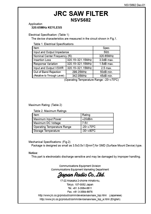
17-22 Akasaka 2-chome minato-ku, Tokyo. 107-0052 JapanTel. +81 3-3584-8811Fax. +81 3-3584-8876Notice1. Use this component within operating temperature range. It might not besatisfied with electrical specification without operating temperature range.When it is used less than -20ºC or more than +70ºC, it might be a cause of degradation or destruction of the component. Even if it endures during a short time, it causes degradation of qualification.2. When soldering iron is used, solder with the temperature at the tip of solderingiron: 350ºC max., the time of soldering: 10 seconds max., the power of soldering iron: 30W max..3. Notice that the allowed time of soldering with soldering iron is accumulatedtime, when soldering is repeated.4. As rapid temperature change for cleaning after reflow soldering might be acause of destruction clean this component after confirming that temperature of this component goes down to room temperature.5. Confirm that there are not any influence for qualification to this component inmounting on PCB when this component is cleaned.6. As it might be a cause of degradation of destruction to apply static electricity tothis component, do not apply static electricity or excessive voltage while assembling and measuring. And do not transport this component with bare hand.7. As it might be a cause of degradation or destruction to apply D.C. voltagebetween each terminal, apply D.C. voltage 7.5V max. in actual circuit.Note1. This specification specifies the quality of this component as a single unit. Makesure that this component is evaluated and confirmed against this specification when it is mounted to your products.。
BD681中文资料
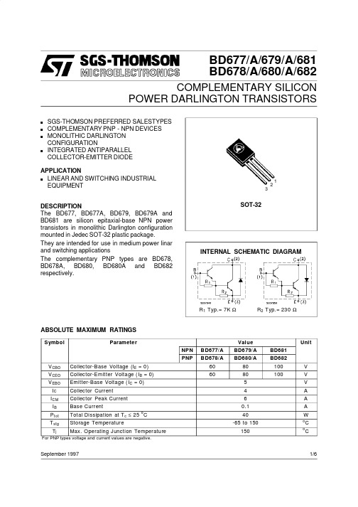
BD677/A/679/A/681BD678/A/680/A/682COMPLEMENTARY SILICONPOWER DARLINGTON TRANSISTORSs SGS-THOMSON PREFERRED SALESTYPES s COMPLEMENTARY PNP -NPN DEVICES sMONOLITHIC DARLINGTON CONFIGURATIONsINTEGRATED ANTIPARALLEL COLLECTOR-EMITTER DIODEAPPLICATION s LINEAR AND SWITCHING INDUSTRIAL EQUIPMENT DESCRIPTIONThe BD677,BD677A,BD679,BD679A and BD681are silicon epitaxial-base NPN power transistors in monolithic Darlington configuration mounted in Jedec SOT-32plastic package.They are intended for use in medium power linar and switching applicationsThe complementary PNP types are BD678,BD678A,BD680,BD680A and BD682respectively.INTERNAL SCHEMATIC DIAGRAMR 1Typ.=7K ΩR 2Typ.=230ΩSeptember 1997ABSOLUTE MAXIMUM RATINGSSymbolParameterValueUnitNPN BD677/A BD679/A BD681PNPBD678/ABD680/ABD682V CBO Collector-Base Voltage (I E =0)6080100V V CEO Collector-Emitter Voltage (I B =0)6080100V V EBO Emitter-Base Voltage (I C =0)5V I C Collector Current 4A I CM Collector Peak Current 6A I B Base Current0.1A P t ot Total Dissipation at T c ≤25oC 40WT stg Storage Temperature-65to 150o C T jMax.Operating Junction Temperature150oCFor PNP types voltage and current values are negative.321SOT-321/6THERMAL DATAR t hj-ca se R t hj-amb Thermal Resistance Junction-case MaxThermal Resistance Junction-ambient Max3.12100o C/Wo C/WELECTRICAL CHARACTERISTICS(T case=25o C unless otherwise specified)Symbol Parameter Test Conditions Min.Typ.Max.UnitI CBO Collector Cut-offCurrent(I E=0)V CE=rated V CBOV CE=rated V CBO T C=100o C0.22mAmAI CEO Collector Cut-offCurrent(I B=0)V CE=half rated V CEO0.5mAI EBO Emitter Cut-off Current(I C=0)V EB=5V2mAV CEO(sus)∗Collector-EmitterSustaining VoltageI C=50mAfor BD677/677A/678/678Afor BD679/679A/680/680Afor BD681/6826080100VVVV CE(sat)∗Collector-EmitterSaturation Voltagefor BD677/678/679/680/681/682I C=1.5A I B=30mAfor BD677A/678A/679A/680AI C=2A I B=40mA2.52.8VVV BE∗Base-Emitter Voltage for BD677/678/679/680/681/682I C=1.5A V CE=3Vfor BD677A/678A/679A/680AI C=2A V CE=3V2.52.5VVh FE∗DC Current Gain for BD677/678/679/680/681/682I C=1.5A V CE=3Vfor BD677A/678A/679A/680AI C=2A V CE=3V750750h f e Small Signal CurrentGainI C=1.5A V CE=3V f=1MHz1∗ Pulsed:Pulse duration=300µs,duty cycle1.5%Safe Operating Areas Derating Curve BD677/677A/678/678A/679/679A/680/680A/681/6822/6DC Current Gain(NPN type)Collector-Emitter Saturation Voltage(NPN type) Base-Emitter Saturation Voltage(NPN type)DC Current Gain(PNP type)Collector-Emitter Saturation Voltage(PNP type) Base-Emitter Saturation Voltage(PNP type)BD677/677A/678/678A/679/679A/680/680A/681/6823/6BD677/677A/678/678A/679/679A/680/680A/681/682Base-Emitter On Voltage(NPN type)Base-Emitter On Voltage(PNP type) Freewheel Diode Forward Voltage(NPN types)Freewheel Diode Forward Voltage(PNP types)4/6DIM.mm inch MIN.TYP.MAX.MIN.TYP.MAX.A 7.47.80.2910.307B 10.510.80.4130.445b 0.70.90.0280.035b10.490.750.0190.030C 2.4 2.70.0400.106c1 1.0 1.30.0390.050D 15.416.00.6060.629e 2.20.087e3 4.154.650.1630.183F 3.80.150G 3 3.20.1180.126H 2.540.100H22.150.084H20016114SOT-32(TO-126)MECHANICAL DATABD677/677A/678/678A/679/679A/680/680A/681/6825/6BD677/677A/678/678A/679/679A/680/680A/681/682Information furnished is believed to be accurate and reliable.However,SGS-THOMSON Microelectronics assumes no responsability for the consequences of use of such information nor for any infringementof patents or other rights of third parties which may results from its use.No license is granted by implication or otherwise under any patent or patent rights of SGS-THOMSON Microelectronics.Specifications mentioned in this publication are subject to change without notice.This publicationsupersedes and replaces all information previously supplied.SGS-THOMSON Microelectronics products are notauthorized for use as critical components in life support devices or systems without express written approval of SGS-THOMSON Microelectonics.©1997SGS-THOMSON Microelectronics-Printed in Italy-All Rights ReservedSGS-THOMSON Microelectronics GROUP OF COMPANIESAustralia-Brazil-Canada-China-France-Germany-Hong Kong-Italy-Japan-Korea-Malaysia-Malta-Morocco-The Netherlands-Singapore-Spain-Sweden-Switzerland-Taiwan-Thailand-United Kingdom-U.S.A...6/6。
BZD27C6V2P中文资料
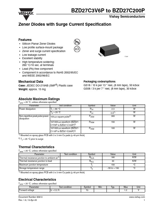
Document Number 17249Zener Diodes with Surge Current SpecificationFeatures•Sillicon Planar Zener Diodes•Low profile surface-mount package•Zener and surge current specification •Low leakage current •Excellent stability•High temperature soldering:260°C/10 sec. at terminals •Lead (Pb)-free component•Component in accordance to RoHS 2002/95/EC and WEEE 2002/96/ECMechanical DataCase: JEDEC DO-219AB (SMF ®) Plastic case Weight: approx. 15 mgPackaging codes/options:GS18 / 10 k per 13 " reel, (8 mm tape), 50 k/box GS08 / 3 k per 7 " reel, (8 mm tape), 30 k/boxAbsolute Maximum RatingsT amb = 25°C, unless otherwise specified1)Mounted on epoxy-glass PCB with 3 x 3 mm Cu pads (≥ 40 µm thick)2) T J= 25°C prior to surgeThermal CharacteristicsT amb = 25°C, unless otherwise specified1)Mounted on epoxy-glass PCB with 3 x 3 mm Cu pads (≥ 40 µm thick)Electrical CharacteristicsT amb = 25°C, unless otherwise specifiedParameterT est conditionSymbol Value Unit Power dissipationT L = 80°C P tot 2.3W T A = 25°CP tot 0.81)W Non-repetitive peak pulse power dissipation100 µs square pulse 2)P ZSM 300W 10/1000 µs waveform (BZD27-C7V5P to BZD27-C100P)2)P RSM 150W 10/1000 µs waveform (BZD27-C110P to BZD27-C200P)2)P RSM100WParameterTest condition Symbol Value Unit Thermal resistance junction to ambient air 1)R thJA 180K/W Thermal resistance junction to lead R thJL 30K/W Maximum junction temperature T j 150°C Storage temperature rangeT S- 55 to + 150°CParameterT est conditionSymbol MinT yp.Max Unit Forward voltage I F = 0.2 AV F1.2V Document Number 85810Electrical CharacteristicsWhen used as voltage regulator diodes (T J = 25°C unless otherwise noted)1)Pulse test: tp ≤ 5 ms.PartnumberMarking CodeWorking Voltage 1)Differential Resistance Temperature Coefficient T est Current Reverse Current at Reverse Voltage V Z @ I ZTr dif @ I ZαZ @ I Z I ZT I R V R V Ω%/°C mA µA Vminmax typ max min max max BZD27C3V6P D0 3.4 3.848-0.14-0.041001001BZD27C3V9P D1 3.7 4.148-0.14-0.04100501BZD27C4V3P D24 4.647-0.12-0.02100251BZD27C4V7P D3 4.4537-0.10100101BZD27C5V1P D4 4.8 5.436-0.080.0210051BZD27C5V6P D5 5.2624-0.040.04100102BZD27C6V2P D6 5.8 6.623-0.010.0610052BZD27C6V8P D7 6.47.21300.07100103BZD27C7V5P D877.91200.07100503BZD27C8V2P D97.78.7120.030.08100103BZD27C9V1P E08.59.6240.030.0850105BZD27C10P E19.410.6240.050.095077.5BZD27C11P E210.411.6470.050.15048.2BZD27C12P E311.412.7470.050.15039.1BZD27C13P E412.414.15100.050.150210BZD27C15P E513.815.65100.050.150111BZD27C16P E615.317.16150.060.1125112BZD27C18P E716.819.16150.060.1125113BZD27C20P E818.821.26150.060.1125115BZD27C22P E920.823.36150.060.1125116BZD27C24P F022.825.67150.060.1125118BZD27C27P F125.128.97150.060.1125120BZD27C30P F228328150.060.1125122BZD27C33P F331358150.060.1125124BZD27C36P F4343821400.060.1110127BZD27C39P F5374121400.060.1110130BZD27C43P F6404624450.070.1210133BZD27C47P F7445024450.070.1210136BZD27C51P F8485425600.070.1210139BZD27C56P F9526025600.070.1210143BZD27C62P G0586625800.080.1310147BZD27C68P G1647225800.080.1310151BZD27C75P G27079301000.080.1310156BZD27C82P G37787301000.080.1310162BZD27C91P G48596602000.080.135168BZD27C100P G594106602000.090.135175BZD27C110P G6104116802500.090.135182BZD27C120P G7114127802500.090.135191BZD27C130P G81241411103000.090.1351100BZD27C150P G91381561303000.090.1351110BZD27C160P H01531711503500.090.1351120BZD27C180P H11681911804000.090.1351130BZD27C200PH21882122005000.090.1351150Document Number Electrical CharacteristicsWhen used as protection diodes (T J = 25°C unless otherwise noted)1)Non-repetitive peak reverse current in accordance with "IEC 60-1, Section 8" (10/1000 µs pulse); see Fig. 5.PartnumberRev. Breakdown Voltage Test Current T emperature Coefficient Clamping VoltageReverse Current at Stand-Off Voltage V (BR)R at I testI test αZ @ I test V C at I RSM 1)I R at V WMV mA%/°C V A µA V minminmax max max BZD27C7V5P 710000.0711.313.31500 6.2BZD27C8V2P 7.71000.030.0812.312.21200 6.8BZD27C9V1P 8.5500.030.0813.311.31007.5BZD27C10P 9.4500.050.0914.810.1208.2BZD27C11P 10.4500.050.115.79.659.1BZD27C12P 11.4500.050.1178.8510BZD27C13P 12.4500.050.118.97.9511BZD27C15P 13.8500.050.120.97.2512BZD27C16P 15.3250.060.1122.9 6.6513BZD27C18P 16.8250.060.1125.6 5.9515BZD27C20P 18.8250.060.1128.4 5.3516BZD27C22P 20.8250.060.1131 4.8518BZD27C24P 22.8250.060.1133.8 4.4520BZD27C27P 25.1250.060.1138.1 3.9522BZD27C30P 28250.060.1142.2 3.6524BZD27C33P 31250.060.1146.2 3.2527BZD27C36P 34100.060.1150.13530BZD27C39P 37100.060.1154.1 2.8533BZD27C43P 40100.070.1260.7 2.5536BZD27C47P 44100.070.1265.5 2.3539BZD27C51P 48100.070.1270.8 2.1543BZD27C56P 52100.070.1278.6 1.9547BZD27C62P 58100.080.1386.5 1.7551BZD27C68P 64100.080.1394.4 1.6556BZD27C75P 70100.080.13103.5 1.5562BZD27C82P 77100.080.13114 1.3568BZD27C91P 8550.090.13126 1.2575BZD27C100P 9450.090.13139 1.1582BZD27C110P 10450.090.131390.72591BZD27C120P 11450.090.131520.655100BZD27C130P 12450.090.131690.595110BZD27C150P 13850.090.131870.535120BZD27C160P 15350.090.132050.485130BZD27C180P 16850.090.132290.435150BZD27C200P18850.090.132540.395160 Document Number 85810Typical Characteristics (Tamb = 25 °C unless otherwise specified)Figure 2. Typ. Diode Capacitance vs. Reverse Voltage Figure 3. Power Dissipation vs. Ambient Temperature17411F I – F o r w a r d C u r r e n t ( A )0.00.5 1.0 1.5 2.0 2.5 3.017412C – T y p . J u n c t i o n C a p a c i t a n c e ( p F )D V R – Reverse Voltage (V)0.00.51.01.52.02.53.00255075100125150T amb – Ambient T emperature ( q C )17413P –P o w e r D i s s i p a t i o n ( W )t o t Figure 4. Maximum Pulse Power Dissipation vs. Zener VoltageFigure 5. Non-Repetitive Peak Reverse Current Pulse Definition0204060801001201401600255075100125150175200V Znom – Zener Voltage ( V )17414P –M a x . P u l s e P o w e r D i s s i p a t i o n ( W )R S M IPackage Dimensions in mm (Inches)Document Number Blistertape for SMF Document Number 85810Ozone Depleting Substances Policy StatementIt is the policy of Vishay Semiconductor GmbH to1.Meet all present and future national and international statutory requirements.2.Regularly and continuously improve the performance of our products, processes, distribution and operatingsystems with respect to their impact on the health and safety of our employees and the public, as well as their impact on the environment.It is particular concern to control or eliminate releases of those substances into the atmosphere which are known as ozone depleting substances (ODSs).The Montreal Protocol (1987) and its London Amendments (1990) intend to severely restrict the use of ODSs and forbid their use within the next ten years. Various national and international initiatives are pressing for an earlier ban on these substances.Vishay Semiconductor GmbH has been able to use its policy of continuous improvements to eliminate the use of ODSs listed in the following documents.1.Annex A, B and list of transitional substances of the Montreal Protocol and the London Amendmentsrespectively2.Class I and II ozone depleting substances in the Clean Air Act Amendments of 1990 by the EnvironmentalProtection Agency (EPA) in the USA3.Council Decision 88/540/EEC and 91/690/EEC Annex A, B and C (transitional substances) respectively. Vishay Semiconductor GmbH can certify that our semiconductors are not manufactured with ozone depleting substances and do not contain such substances.We reserve the right to make changes to improve technical designand may do so without further notice.Parameters can vary in different applications. All operating parameters must be validated for each customer application by the customer. Should the buyer use Vishay Semiconductors products for any unintended or unauthorized application, the buyer shall indemnify Vishay Semiconductors against all claims, costs, damages, and expenses, arising out of, directly or indirectly, any claim of personal damage, injury or death associated with such unintended or unauthorized use.Vishay Semiconductor GmbH, P.O.B. 3535, D-74025 Heilbronn, GermanyDocument Number 。
BD236中文资料
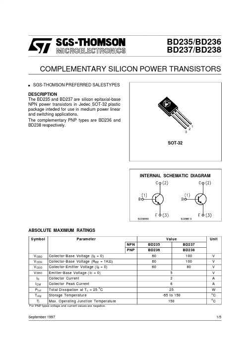
BD235/BD236BD237/BD238COMPLEMENTARY SILICON POWER TRANSISTORSsSGS-THOMSON PREFERRED SALESTYPESDESCRIPTIONThe BD235and BD237are silicon epitaxial-base NPN power transistors in Jedec SOT-32plastic package inteded for use in medium power linear and switching applications.The complementary PNP types are BD236and BD238respectively.INTERNAL SCHEMATIC DIAGRAMSeptember 1997ABSOLUTE MAXIMUM RATINGSSymbolParameterValueUnitNPN BD235BD237PNPBD236BD238V CBO Collector-Base Voltage (I E =0)60100V V CER Collector-Base Voltage (R BE =1K Ω)60100V V CEO Collector-Emitter Voltage (I B =0)6080V V EBO Emitter-Base Voltage (I C =0)5V I C Collector Current 2A I CM Collector Peak Current 6A P t ot Total Dissipation at T c =25oC 25WT stg Storage Temperature-65to 150o C T jMax.Operating Junction Temperature150oCFor PNP types voltage and current values are negative.321SOT-321/5THERMAL DATAR t hj-ca se Thermal Resistance Junction-case Max5o C/W ELECTRICAL CHARACTERISTICS(T case=25o C unless otherwise specified)Symbol Parameter Test Conditions Min.Typ.Max.UnitI CBO Collector Cut-offCurrent(I E=0)V CE=rated V CEOV CE=rated V CEO T c=150o C0.12mAmAI EBO Emitter Cut-off Current(I C=0)V EB=5V1mAV CEO(sus)∗Collector-EmitterSustaining Voltage I C=100mAfor BD235/BD236for BD237/BD2386080VVV CE(sat)∗Collector-EmitterSaturation VoltageI C=1A I B=0.1A0.6V V BE∗Base-Emitter Voltage I C=1A V CE=2V 1.3Vh FE∗DC Current Gain I C=150mA V CE=2VI C=1A V CE=2V 40 25f T Transition frequency I C=250mA V CE=10V3MHz h FE1/h FE2∗Matched Pairs I C=150mA V CE=2V 1.6∗ Pulsed:Pulse duration=300µs,duty cycle1.5%Safe Operating Area Derating CurvesBD235/BD236/BD237/BD2382/5DC Current Gain(NPN type)Collector-Emitter Saturation Voltage(NPN type) Base-Emitter Saturation Voltage(NPN type)DC Current Gain(PNP type)Collector-Emitter Saturation Voltage(PNP type) Collector-Base Capacitance(PNP type)BD235/BD236/BD237/BD2383/5DIM.mm inch MIN.TYP.MAX.MIN.TYP.MAX.A 7.47.80.2910.307B 10.510.80.4130.445b 0.70.90.0280.035b10.490.750.0190.030C 2.4 2.70.0400.106c1 1.0 1.30.0390.050D 15.416.00.6060.629e 2.20.087e3 4.154.650.1630.183F 3.80.150G 3 3.20.1180.126H 2.540.100H22.150.084H20016114SOT-32(TO-126)MECHANICAL DATABD235/BD236/BD237/BD2384/5BD235/BD236/BD237/BD238 Information furnished is believed to be accurate and reliable.However,SGS-THOMSON Microelectronics assumes no responsability for the consequences of use of such information nor for any infringementof patents or other rights of third parties which may results from its use.No license is granted by implication or otherwise under any patent or patent rights of SGS-THOMSON Microelectronics.Specifications mentionedin this publication are subject to change without notice.This publicationsupersedes and replaces all information previously supplied.SGS-THOMSON Microelectronics products are notauthorized for use as critical components in life support devices or systems without express written approval of SGS-THOMSON Microelectonics.©1997SGS-THOMSON Microelectronics-Printed in Italy-All Rights ReservedSGS-THOMSON Microelectronics GROUP OF COMPANIESAustralia-Brazil-Canada-China-France-Germany-Hong Kong-Italy-Japan-Korea-Malaysia-Malta-Morocco-The Netherlands-Singapore-Spain-Sweden-Switzerland-Taiwan-Thailand-United Kingdom-U.S.A...5/5。
D63LCB中文资料
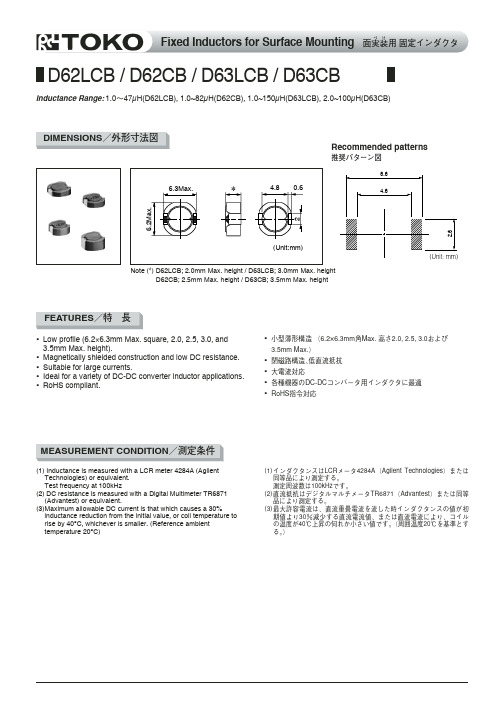
DIMENSIONSFEATURESMEASUREMENT CONDITIOND62LCB / D62CB / D63LCB / D63CBRecommended patterns•Low profile (6.2×6.3mm Max. square, 2.0, 2.5, 3.0,and 3.5mm Max. height).•Magnetically shielded construction and low DC resistance.•Suitable for large currents.•Ideal for a variety of DC-DC converter inductor applications.•RoHS compliant.• ו •• •Note (*) D62LCB; 2.0mm Max. height / D63LCB; 3.0mm Max. heightD62CB; 2.5mm Max. height / D63CB; 3.5mm Max. height(1) Inductance is measured with a LCR meter 4284A (Agilent Technologies) or equivalent.Test frequency at 100kHz(2) DC resistance is measured with a Digital Multimeter TR6871(Advantest) or equivalent.(3)Maximum allowable DC current is that which causes a 30%inductance reduction from the initial value, or coil temperature to rise by 40°C, whichever is smaller. (Reference ambient temperature 20°C)6.2M a x .6.3Max.24.80.6(Unit:mm)4.62.66.6(Unit: mm)#A920CY-1R0M 1.0± 2014 (11)2.89 (3.85) 3.48 (4.64) 4.31 (5.07)#A920CY-1R5M 1.5± 2017 (14) 2.35 (3.18) 2.83 (3.77) 3.68 (4.33)#A920CY-2R0M 2.0± 2021 (17) 2.03 (2.73) 2.44 (3.25) 3.54 (4.17)#A920CY-3R3M 3.3± 20 29 (24) 1.57 (2.03) 1.89 (2.52) 2.73 (3.22)#A920CY-4R3M 4.3± 20 37 (31) 1.37 (1.73) 1.65 (2.20) 2.46 (2.90)TYPE D62CB (With Ferrite shield) (Quantity/reel; 1,500 PCS)TOKO Part Number Inductance Decrease Current (3)(A) Max. (Typ.)=10%=30%∆LL ∆L L TemperatureRise Current (3)∆T=40°C (A)Max. (Typ.)#A920CY-6R2M 6.2± 2052 (43) 1.14 (1.47) 1.37 (1.82) 1.85 (2.18)#A920CY-100M 10.0± 2077 (64)0.89 (1.19) 1.07 (1.42) 1.55 (1.83)#A920CY-120M 12.0± 2090 (75)0.81 (1.10)0.97 (1.29) 1.38 (1.62)#A920CY-150M 15.0± 20105 (87)0.73 (1.02)0.87 (1.16) 1.25 (1.47)#A920CY-180M 18.0± 20129 (110)0.66 (0.90)0.79 (1.05) 1.16 (1.37)#A920CY-220M 22.0± 20154 (130)0.60 (0.83)0.71 (0.94) 1.01 (1.19)#A920CY-270M 27.0± 20 204 (170)0.54 (0.77)0.64 (0.85)0.94 (1.11)#A920CY-330M 33.0± 20229 (195)0.49 (0.63)0.58 (0.77)0.84 (0.99)#A920CY-390M 39.0± 20 294 (245)0.45 (0.58)0.53 (0.70)0.74 (0.87)#A920CY-470M 47.0± 20 348 (290)0.40 (0.55)0.48 (0.64)0.68 (0.80)#A920CY-560M 56.0± 20 413 (345)0.37 (0.49)0.44 (0.58)0.63 (0.74)#A920CY-680M 68.0± 20 475 (400)0.33 (0.48)0.40 (0.53)0.59 (0.69)#A920CY-820M82.0± 20558 (465)0.30 (0.42)0.36 (0.48)0.56 (0.66)Inductance (1)(µH)Tolerance(%)DC Resistance (2)(m Ω) Max.(Typ.)SELECTION GUIDE FOR STANDARD COILS#A918CY-1R0M #A918CY-1R5M #A918CY-2R0M #A918CY-3R3M #A918CY-4R7M TemperatureRise Current (3)∆T=40°C (A)Max. (Typ.)1.0± 2017 (14)2.97 (3.95) 3.50 (4.67) 3.70 (4.35)1.5± 2021 (17) 2.48 (3.30) 2.94 (3.92) 3.17 (3.74)2.0± 2029 (24) 2.06 (2.74) 2.47 (3.30) 2.47 (2.91)3.3± 20 47 (39) 1.65 (2.20) 1.99 (2.65) 2.10 (2.47)4.7± 20 66 (55) 1.33 (1.77) 1.59 (2.11) 1.63 (1.93)TYPE D62LCB (With Ferrite Shield) (Quantity/reel; 1,500 PCS)TOKO Part Number 6.2± 2074 (62) 1.25 (1.67) 1.49 (1.99) 1.53 (1.81)8.2± 20102 (85) 1.03 (1.38) 1.25 (1.66) 1.31 (1.54)10.0± 20118 (98) 1.01 (1.35) 1.22 (1.62) 1.15 (1.36)12.0± 20154 (128)0.82 (1.10)0.99 (1.32) 1.17 (1.38)15.0± 20179 (149)0.79 (1.06)0.94 (1.25)0.87 (1.03)#A918CY-6R2M #A918CY-8R2M #A918CY-100M #A918CY-120M #A918CY-150M 18.0± 20207 (172)0.70 (0.93)0.83 (1.11)0.95 (1.12)22.0± 20 253 (211)0.67 (0.89)0.80 (1.06)0.78 (0.92)27.0± 20331 (275)0.55 (0.73)0.65 (0.87)0.68 (0.81)33.0± 20 368 (306)0.54 (0.72)0.63 (0.85)0.64 (0.76)39.0± 20 473 (394)0.46 (0.61)0.55 (0.73)0.59 (0.70)#A918CY-180M #A918CY-220M #A918CY-270M #A918CY-330M #A918CE-390M 47.0± 20542 (452)0.42 (0.57)0.50 (0.67)0.55 (0.65)#A918CE-470MInductance (1)(µH)DC Resistance (2)(m Ω) Max.(Typ.)Inductance Decrease Current (3)(A) Max. (Typ.)=10%=30%∆LL ∆L L Tolerance(%)#A921CY-1R0M 1.0± 2014 (11)2.95 (4.06)3.59 (4.79) 4.52 (5.32)#A921CY-1R5M 1.5± 2016 (13) 2.41 (3.35) 2.93 (3.92) 3.78 (4.45)#A921CY-2R2M 2.2± 2020 (16) 1.99 (2.72) 2.42 (3.24) 3.51 (4.13)#A921CY-3R6M 3.6± 20 26 (21) 1.55 (2.00) 1.89 (2.53) 3.01 (3.54)#A921CY-4R7M 4.7± 20 33 (27) 1.36 (1.70) 1.66 (2.22) 2.58 (3.03)TYPE D63LCB (With Ferrite Shield) (Quantity/reel; 1,500 PCS)TOKO Part Number DC Resistance (2)(m Ω) Max.(Typ.)Inductance Decrease Current (3)(A) Max. (Typ.)=10%=30%∆LL ∆L L Temperature Rise Current (3)∆T=40°C (A)Max. (Typ.)#A921CY-6R2M 6.2± 2039 (32) 1.18 (1.58) 1.45 (1.93) 2.28 (2.69)#A921CY-100M 10.0± 2059 (49)0.93 (1.22) 1.14 (1.52) 1.91 (2.25)#A921CY-120M 12.0± 2063 (52)0.85 (1.10) 1.04 (1.39) 1.80 (2.12)#A921CY-150M 15.0± 2075 (62)0.76 (1.02)0.93 (1.25) 1.73 (2.04)#A921CY-180M 18.0± 2089 (74)0.69 (0.93)0.85 (1.14) 1.58 (1.86)#A921CY-220M 22.0± 20115 (95)0.62 (0.80)0.77 (1.03) 1.34 (1.58)#A921CY-270M 27.0± 20 144 (120)0.56 (0.74)0.70 (0.93) 1.14 (1.35)#A921CY-330M 33.0± 20168 (140)0.51 (0.70)0.63 (0.84) 1.01 (1.19)#A921CY-390M 39.0± 20 180 (150)0.47 (0.66)0.58 (0.77)0.98 (1.16)#A921CY-470M 47.0± 20 225 (185)0.43 (0.56)0.53 (0.71)0.89 (1.05)#A921CY-560M 56.0± 20 264 (220)0.39 (0.52)0.48 (0.65)0.82 (0.97)#A921CY-680M 68.0± 20 324 (270)0.35 (0.45)0.44 (0.59)0.73 (0.87)#A921CY-820M 82.0± 20 396 (330)0.32 (0.44)0.40 (0.54)0.64 (0.76)#A921CY-101M 100.0± 20 498 (415)0.29 (0.40)0.36 (0.49)0.58 (0.69)#A921CY-151M150.0± 20738 (615)0.25 (0.33)0.31 (0.41)0.44 (0.52)Inductance (1)(µH)Tolerance(%)D63LCB :6.2×6.3mm Max. square, 3.0mm height, Inductance range: 1.0~150µH D63CB : 6.2×6.3mm Max. square, 3.5mm height, Inductance range: 2.0~100µHSELECTION GUIDE FOR STANDARD COILSTemperatureRise Current (3)∆T=40°C (A)Max. (Typ.)2.0± 2019 (16)2.36 (3.15) 3.00 (4.00) 3.51 (4.14)2.7± 2022 (18) 2.17 (2.89) 2.69 (3.59) 3.32 (3.91)3.3± 2026 (21) 2.10 (2.80) 2.57 (3.43) 2.99 (3.52)4.7± 20 32 (26) 1.65 (2.20) 2.08 (2.78) 2.67 (3.15)6.2± 20 35 (29) 1.41 (1.88) 1.84 (2.45) 2.56 (3.02)TYPE D63CB (With Ferrite Shield) (Quantity/reel; 1,000 PCS)TOKO Part Number #A916CY-2R0M #A916CY-2R7M #A916CY-3R3M #A916CY-4R7M #A916CY-6R2M 8.2± 2044 (36) 1.25 (1.66) 1.54 (2.06) 2.24 (2.64)10.0± 2050 (41) 1.15 (1.53) 1.49 (1.99) 2.09 (2.46)12.0± 2062 (52)0.98 (1.31) 1.28 (1.71) 1.84 (2.17)15.0± 2077 (64)0.86 (1.14) 1.10 (1.47) 1.64 (1.93)18.0± 2082 (68)0.80 (1.07) 1.05 (1.40) 1.61 (1.90)#A916CY-8R2M #A916CY-100M #A916CY-120M #A916CY-150M #A916CY-180M 22.0± 20106 (88)0.75 (0.99)0.97 (1.29) 1.37 (1.62)27.0± 20 140 (117)0.64 (0.85)0.82 (1.09) 1.18 (1.39)33.0± 20162 (135)0.60 (0.80)0.76 (1.01) 1.09 (1.28)39.0± 20 191 (159)0.55 (0.74)0.70 (0.93) 1.02 (1.20)47.0± 20 208 (174)0.53 (0.70)0.68 (0.90)0.95 (1.12)#A916CY-220M #A916CY-270M #A916CY-330M #A916CY-390M #A916CY-470M 56.0± 20 257 (214)0.47 (0.63)0.60 (0.80)0.85 (1.00)68.0± 20 319 (266)0.44 (0.58)0.56 (0.74)0.75 (0.89)82.0± 20 420 (349)0.36 (0.48)0.47 (0.62)0.65 (0.76)100.0± 20477 (397)0.36 (0.48)0.45 (0.60)0.60 (0.71)#A916CY-560M #A916CY-680M #A916CY-820M #A916CY-101MInductance (1)(µH)DC Resistance (2)(m Ω) Max.(Typ.)Inductance Decrease Current (3)(A) Max. (Typ.)=10%=30%∆LL ∆L L Tolerance(%)。
- 1、下载文档前请自行甄别文档内容的完整性,平台不提供额外的编辑、内容补充、找答案等附加服务。
- 2、"仅部分预览"的文档,不可在线预览部分如存在完整性等问题,可反馈申请退款(可完整预览的文档不适用该条件!)。
- 3、如文档侵犯您的权益,请联系客服反馈,我们会尽快为您处理(人工客服工作时间:9:00-18:30)。
BD677/A/679/A/681BD678/A/680/A/682COMPLEMENTARY SILICONPOWER DARLINGTON TRANSISTORSs SGS-THOMSON PREFERRED SALESTYPES s COMPLEMENTARY PNP -NPN DEVICES sMONOLITHIC DARLINGTON CONFIGURATIONsINTEGRATED ANTIPARALLEL COLLECTOR-EMITTER DIODEAPPLICATION s LINEAR AND SWITCHING INDUSTRIAL EQUIPMENT DESCRIPTIONThe BD677,BD677A,BD679,BD679A and BD681are silicon epitaxial-base NPN power transistors in monolithic Darlington configuration mounted in Jedec SOT-32plastic package.They are intended for use in medium power linar and switching applicationsThe complementary PNP types are BD678,BD678A,BD680,BD680A and BD682respectively.INTERNAL SCHEMATIC DIAGRAMR 1Typ.=7K ΩR 2Typ.=230ΩSeptember 1997ABSOLUTE MAXIMUM RATINGSSymbolParameterValueUnitNPN BD677/A BD679/A BD681PNPBD678/ABD680/ABD682V CBO Collector-Base Voltage (I E =0)6080100V V CEO Collector-Emitter Voltage (I B =0)6080100V V EBO Emitter-Base Voltage (I C =0)5V I C Collector Current 4A I CM Collector Peak Current 6A I B Base Current0.1A P t ot Total Dissipation at T c ≤25oC 40WT stg Storage Temperature-65to 150o C T jMax.Operating Junction Temperature150oCFor PNP types voltage and current values are negative.321SOT-321/6THERMAL DATAR t hj-ca se R t hj-amb Thermal Resistance Junction-case MaxThermal Resistance Junction-ambient Max3.12100o C/Wo C/WELECTRICAL CHARACTERISTICS(T case=25o C unless otherwise specified)Symbol Parameter Test Conditions Min.Typ.Max.UnitI CBO Collector Cut-offCurrent(I E=0)V CE=rated V CBOV CE=rated V CBO T C=100o C0.22mAmAI CEO Collector Cut-offCurrent(I B=0)V CE=half rated V CEO0.5mAI EBO Emitter Cut-off Current(I C=0)V EB=5V2mAV CEO(sus)∗Collector-EmitterSustaining VoltageI C=50mAfor BD677/677A/678/678Afor BD679/679A/680/680Afor BD681/6826080100VVVV CE(sat)∗Collector-EmitterSaturation Voltagefor BD677/678/679/680/681/682I C=1.5A I B=30mAfor BD677A/678A/679A/680AI C=2A I B=40mA2.52.8VVV BE∗Base-Emitter Voltage for BD677/678/679/680/681/682I C=1.5A V CE=3Vfor BD677A/678A/679A/680AI C=2A V CE=3V2.52.5VVh FE∗DC Current Gain for BD677/678/679/680/681/682I C=1.5A V CE=3Vfor BD677A/678A/679A/680AI C=2A V CE=3V750750h f e Small Signal CurrentGainI C=1.5A V CE=3V f=1MHz1∗ Pulsed:Pulse duration=300µs,duty cycle1.5%Safe Operating Areas Derating Curve BD677/677A/678/678A/679/679A/680/680A/681/6822/6DC Current Gain(NPN type)Collector-Emitter Saturation Voltage(NPN type) Base-Emitter Saturation Voltage(NPN type)DC Current Gain(PNP type)Collector-Emitter Saturation Voltage(PNP type) Base-Emitter Saturation Voltage(PNP type)BD677/677A/678/678A/679/679A/680/680A/681/6823/6BD677/677A/678/678A/679/679A/680/680A/681/682Base-Emitter On Voltage(NPN type)Base-Emitter On Voltage(PNP type) Freewheel Diode Forward Voltage(NPN types)Freewheel Diode Forward Voltage(PNP types)4/6DIM.mm inch MIN.TYP.MAX.MIN.TYP.MAX.A 7.47.80.2910.307B 10.510.80.4130.445b 0.70.90.0280.035b10.490.750.0190.030C 2.4 2.70.0400.106c1 1.0 1.30.0390.050D 15.416.00.6060.629e 2.20.087e3 4.154.650.1630.183F 3.80.150G 3 3.20.1180.126H 2.540.100H22.150.084H20016114SOT-32(TO-126)MECHANICAL DATABD677/677A/678/678A/679/679A/680/680A/681/6825/6BD677/677A/678/678A/679/679A/680/680A/681/682Information furnished is believed to be accurate and reliable.However,SGS-THOMSON Microelectronics assumes no responsability for the consequences of use of such information nor for any infringementof patents or other rights of third parties which may results from its use.No license is granted by implication or otherwise under any patent or patent rights of SGS-THOMSON Microelectronics.Specifications mentioned in this publication are subject to change without notice.This publicationsupersedes and replaces all information previously supplied.SGS-THOMSON Microelectronics products are notauthorized for use as critical components in life support devices or systems without express written approval of SGS-THOMSON Microelectonics.©1997SGS-THOMSON Microelectronics-Printed in Italy-All Rights ReservedSGS-THOMSON Microelectronics GROUP OF COMPANIESAustralia-Brazil-Canada-China-France-Germany-Hong Kong-Italy-Japan-Korea-Malaysia-Malta-Morocco-The Netherlands-Singapore-Spain-Sweden-Switzerland-Taiwan-Thailand-United Kingdom-U.S.A...6/6。
