常用串行EEPROM芯片
串行EEPROM AT24CXX芯片资料
串行EEPROM AT24CXX芯片资料AT24CXX是美国ATMEL公司的低功耗CMOS串行EEPROM,典型的型号有AT24C01A/02/04/08/16等5种,它们的存储容量分别是1024/2048/4096/8192/16384位;也就是128/256/512/1024/2048字节;使用电压级别有5V,2.7V,2.5V,1.8V;本文主要介绍常用的AT24C02即256字节存储器的使用;它具有工作电压宽(2.5~5.5V)、擦写次数多(大于10000次)、写入速度快(小于10ms)等特点。
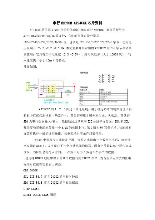
外行如图:AT24C02的1、2、3脚是三条地址线,用于确定芯片的硬件地址(实验板中直接接地只有一块器件);第8脚和第4脚分别为正、负电源。
第5脚SDA为串行数据输入/输出,数据通过这条双向I2C总线串行传送,SDA和SCL都需要和正电源间各接一个5.1K的电阻上拉。
第7脚为WP写保护端,接地时允许芯片执行一般的读写操作。
接电源端时不允许对器件写。
24C02中带有片内地址寄存器。
每写入或读出一个数据字节后,该地址寄存器自动加1,以实现对下一个存储单元的读写。
所有字节均以单一操作方式读取。
为降低总的写入时间,一次操作可写入多达8个字节的数据。
;这是将0100H地址中以下的8个数据写到24C02的01H为首址单元中去的汇编程序可直接在实验板上实验。
ORG 0000HSCL BIT P3.7;定义24C02的串行时钟线SDA BIT P3.6;定义24C02的串行数据线LJMP STARTSTART:LCALL STAR;调用MOV R2,#08H;一个数据有8位MOV DPTR,#0100H;定义源数据的位置LOOP:MOV A,#00HMOVC A,@A+DPTRLCALL SDATALCALL ACKJC LOOPINC DPTRDJNZ R2,LOOPLCALL STOP;调用停止子程序STAR:SETB SDASETB SCLNOPNOPNOPNOPCLR SDANOPNOPNOPNOPCLR SCLRETSDATA:MOV R0,#08HLOOP0:RLC AMOV SDA,CNOPNOPSETB SCLNOPNOPNOPCLR SCLDJNZ R0,LOOP0 RETACK:SETB SDA NOPNOPSETB SCL NOPNOPNOPNOPMOV C,SDA CLR SCLRETSTOP:CLR SDA NOPNOPNOPNOPSETB SCL NOPNOPNOPNOPSETB SDANOPNOPNOPRETORG 0100HDB 0A0H,10H,01H,02H,03H,04H,05H,06HEND读写子程序如下:;写串行E2PROM子程序XEPR; R3=10100000(命令1010+器件3位地址+读/写。
串行eepromat24cxx芯片资料
串行EEPROM AT24CXX芯片资料AT24CXX是美国ATMEL公司的低功耗CMOS串行EEPROM,典型的型号有AT24C01A/02/04/08/16等5种,它们的存储容量分别是1024/2048/4096/8192/16384位;也就是128/256/512/1024/2048字节;使用电压级别有5V,2.7V,2.5V,1.8V;本文主要介绍常用的AT24C02即256字节存储器的使用;它具有工作电压宽(2.5~5.5V)、擦写次数多(大于10000次)、写入速度快(小于10ms)等特点。
外行如图:AT24C02的1、2、3脚是三条地址线,用于确定芯片的硬件地址(实验板中直接接地只有一块器件);第8脚和第4脚分别为正、负电源。
第5脚SDA为串行数据输入/输出,数据通过这条双向I2C总线串行传送,SDA和SCL 都需要和正电源间各接一个5.1K的电阻上拉。
第7脚为WP写保护端,接地时允许芯片执行一般的读写操作。
接电源端时不允许对器件写。
24C02中带有片内地址寄存器。
每写入或读出一个数据字节后,该地址寄存器自动加1,以实现对下一个存储单元的读写。
所有字节均以单一操作方式读取。
为降低总的写入时间,一次操作可写入多达8个字节的数据。
;这是将0100H地址中以下的8个数据写到24C02的01H为首址单元中去的汇编程序可直接在实验板上实验。
ORG 0000HSCL BIT P3.7;定义24C02的串行时钟线SDA BIT P3.6;定义24C02的串行数据线LJMP STARTSTART:LCALL STAR;调用MOV R2,#08H;一个数据有8位MOV DPTR,#0100H;定义源数据的位置LOOP:MOV A,#00HMOVC A,@A+DPTRLCALL SDATALCALL ACKJC LOOPINC DPTRDJNZ R2,LOOPLCALL STOP;调用停止子程序STAR:SETB SDASETB SCLNOPNOPNOPNOPCLR SDANOPNOPNOPNOPCLR SCLRETSDATA:MOV R0,#08HLOOP0:RLC AMOV SDA,CNOPNOPSETB SCLNOPNOPNOPCLR SCLDJNZ R0,LOOP0 RETACK:SETB SDA NOPNOPSETB SCL NOPNOPNOPNOPMOV C,SDA CLR SCLRETSTOP:CLR SDA NOPNOPNOPNOPSETB SCL NOPNOPNOPNOPSETB SDANOPNOPNOPRETORG 0100HDB 0A0H,10H,01H,02H,03H,04H,05H,06HEND读写子程序如下:;写串行E2PROM子程序XEPR; R3=10100000(命令1010+器件3位地址+读/写。
24c16读写程序详解

24c16读写程序详解24C16是一种常见的串行EEPROM芯片,可用于存储数据。
本文将详细介绍24C16的读写程序,包括读取和写入数据的步骤和方法。
24C16是一款16K位的串行EEPROM芯片,它具有256字节的存储容量。
它被广泛应用于各种电子设备中,如智能卡、计算机、嵌入式系统等。
本文将以一个简单的例子来说明24C16的读写程序。
我们需要连接24C16芯片到我们的系统中。
通常,我们使用I2C总线来与芯片进行通信。
在开始之前,我们需要确定芯片的I2C地址。
24C16有两个地址引脚(A0和A1),通过这两个引脚可以设置芯片的地址。
根据这两个引脚的连接方式,可以得到芯片的地址。
例如,如果我们将A0和A1引脚都接地,那么芯片的地址将是0x50。
接下来,我们需要编写读取数据的程序。
首先,我们需要发送起始信号,然后发送芯片的地址和读取命令。
然后,我们可以连续读取数据,直到读取完所有数据。
读取数据的过程如下所示:1. 发送起始信号2. 发送芯片地址和读取命令3. 读取数据4. 发送应答信号5. 重复步骤3和4,直到读取完所有数据6. 发送停止信号写入数据的程序与读取数据的程序类似。
首先,我们发送起始信号和芯片地址。
然后,我们发送写入命令和要写入的数据。
写入数据的过程如下所示:1. 发送起始信号2. 发送芯片地址和写入命令3. 发送要写入的数据4. 发送停止信号需要注意的是,写入数据时需要等待一段时间,以确保数据已经写入到芯片中。
在等待的过程中,我们可以执行其他的操作。
以上就是24C16的读写程序的详细介绍。
在实际应用中,我们可以根据具体的需求对读写程序进行优化和扩展。
例如,我们可以添加错误处理机制,以确保数据的完整性和正确性。
另外,我们还可以使用不同的编程语言来编写读写程序,如C、Python等。
总结起来,24C16是一款常见的串行EEPROM芯片,可以用于存储数据。
通过编写读写程序,我们可以方便地读取和写入数据。
m24256 例程

m24256 例程m24256是一款非常常见的串行EEPROM芯片,广泛应用于各种电子设备中。
它具有容量大、速度快、可靠性高等优点,因此备受电子工程师的欢迎和青睐。
本文将介绍m24256的基本特点、工作原理以及在实际应用中的一些注意事项。
让我们来了解一下m24256的基本特点。
m24256是一款2-wire串行EEPROM芯片,容量为256K位,即32K字节。
它采用了I2C总线协议进行数据传输,具有8个地址引脚,可以支持128个设备的级联。
m24256具有高速度的写入和读取操作,写入速度可达5ms,读取速度可达400ns。
此外,m24256还具有低功耗、可靠性高、抗干扰能力强等特点。
接下来,我们来了解一下m24256的工作原理。
m24256的工作分为写入和读取两个过程。
在写入过程中,首先选择所需写入的地址,并将数据送入数据输入引脚。
然后,通过I2C总线发送写入命令,m24256会将数据写入相应的存储单元中。
在读取过程中,同样需要选择所需读取的地址,并发送读取命令。
m24256会将相应的存储单元中的数据送至数据输出引脚,供外部设备读取。
在实际应用中,我们需要注意一些事项。
首先,由于m24256是一款非易失性存储器,因此在写入数据时要谨慎,避免误操作导致数据丢失。
其次,m24256的写入和读取速度较快,但在实际应用中,我们还需要考虑到总线传输速度、外部设备的响应速度等因素,以确保数据的正确性和稳定性。
此外,m24256的地址引脚较多,应根据实际需求进行正确连接。
最后,m24256的工作电压为2.5V至5.5V,应根据实际电源情况选择合适的供电电压。
总的来说,m24256是一款功能强大、性能优越的串行EEPROM芯片。
它具有容量大、速度快、可靠性高等优点,广泛应用于各种电子设备中。
在实际应用中,我们需要注意写入数据的谨慎操作、总线传输速度和外部设备响应速度的匹配、地址引脚的正确连接以及合适的供电电压选择。
EEPROM存储芯片24C02
EEPROM存储芯⽚24C021、24C02简介 24C02是⼀个2Kbit的串⾏EEPROM存储芯⽚,可存储256个字节数据。
⼯作电压范围为1.8V到6.0V,具有低功耗CMOS技术,⾃定时擦写周期,1000000次编程/擦除周期,可保存数据100年。
24C02有⼀个16字节的页写缓冲器和⼀个写保护功能。
通过I2C总线通讯读写芯⽚数据,通讯时钟频率可达400KHz。
可以通过存储IC的型号来计算芯⽚的存储容量是多⼤,⽐如24C02后⾯的02表⽰的是可存储2Kbit的数据,转换为字节的存储量为2*1024/8 = 256byte;有⽐如24C04后⾯的04表⽰的是可存储4Kbit的数据,转换为字节的储存量为2*1024/8 = 512byte;以此来类推其它型号的存储空间。
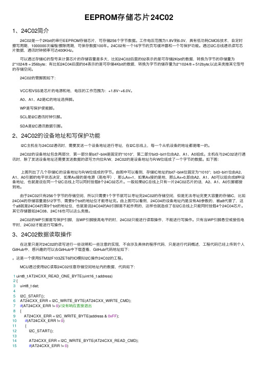
24C02的管脚图如下: VCC和VSS是芯⽚的电源和地,电压的⼯作范围为:+1.8V~+6.0V。
A0、A1、A2是IC的地址选择脚。
WP是写保护使能脚。
SCL是I2C通讯时钟引脚。
SDA是I2C通讯数据引脚。
2、24C02的设备地址和写保护功能 I2C主机在与24C02通讯时,需要发送⼀个设备地址进⾏寻址,在I2C总线上,每⼀个从机设备的地址都是唯⼀的。
24C02的设备地址包含两部分,第⼀部分是bit7~bit4是固定的“1010”,第⼆部分bit3~bit1位由A2、A1、A0组成。
主机在与24C02进⾏通讯时,除了发送设备地址还需要发送数据的读写⽅向位R/W,24C02的是设备地址与R/W位组成了⼀个字节的数据。
如下图: 上图列出了⼏个存储IC的设备地址与R/W位组成的字节。
由图中可以看到,存储IC地址的bit7~bit4位固定为“1010”;bit3~bit1位由A2、A1、A0引脚的电平状态决定,如果Ax接的是电源(⾼电平),那么Ax=1,如果Ax接的是地,那么Ax=0,即由A2、A1、A0可以组合成8种设备地址,也就是说在同⼀个I2C总线上可以同时挂载8个24C02芯⽚。
EEPROM---AT24Cxx应用介绍
EEPROM---AT24Cxx应⽤介绍结论:1、读写AT24CXX芯⽚,根据容量有多种⽅式:⼀、容量为AT24C01~AT24C16,⾸先发送设备地址(8位地址),再发送数据地址(8位地址),再发送或者接受数据。
⼆、AT24C32/AT24C64~AT24C512,⾸先发送设备地址(8位地址),再发送⾼位数据地址,再发送地位数据地址,再发送或者接受数据。
三、容量AT24C1024的芯⽚,是把容量⼀和容量⼆的⽅法结合,设备地址中要⽤⼀位作为数据地址位,存储地址长度是17位。
2、它的设备地址根据容量不同有区别: 1)、AT24C01~AT24C16:这⼀类⼜分为两类,分别为AT24C01/AT24C02和AT24C04~AT24C16;他们的设备地址为⾼7位,低1位⽤来作为读写标⽰位,1为读,0为写。
*1*、AT24C01/AT24C02。
AT24C01/AT24C02的A0、A1、A2引脚作为7位设备地址的低三位,⾼4为固定为1010B,低三位A0、A1、A2确定了AT24CXX的设备地址,所以⼀根I2C线上最⼤可以接8个AT24CXX,地址为1010000B~1010111B。
*2*、AT24C04~AT24C16的 A0、A1、A2只使⽤⼀部分,不⽤的悬空或者接地(数据⼿册中写的是悬空不接)。
举例:AT24C04只⽤A2、A1引脚作为设备地址,另外⼀位A0不⽤悬空,发送地址中对应的这位(A0)⽤来写⼊页寻址的页⾯号,⼀根I2C线上最⼤可以接4个,地址为101000xB~101011xB 2)、AT24C32/AT24C64:和AT24C01/AT24C02⼀样,区别是,发送数据地址变成16位。
注意事项:对AT24C32来说,WP置⾼,则只有四分之⼀受保护,即0x0C00-0x0FFF。
也就是说保护区为1KBytes。
对于低地址的四分之三,则不保护。
所以,如果数据较多时,可以有选择地存储。
串行EEPROM 93C46的操作方法
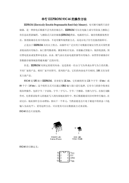
写入一个字(16 位): // Writes memory location An A0. void Write(unsigned char address,unsigned int InData) { unsigned char temp; Ewen(); SK=0; DI=1; // 101 A5A0 CS=0; CS=1; SK=1; SK=0; // 1 address=address&0x3f|0x40; for(temp=8;temp!=0;temp) // 8 { DI=address&0x80; SK=1; SK=0; address<<=1; } for(temp=16;temp!=0;temp) // 16 { DI=InData&0x8000; SK=1; SK=0; InData<<=1; } CS=0; DO=1; CS=1; SK=1; while(DO==0) // busy test { SK=0; SK=1; } SK=0; CS=0; Ewds(); }
数据读取:
数据写入:
93C46 共有七种操作,如下列所示:
指令
功能描述
操作码 ORG=0 字节 数据 ORG=1 字 数据
READ
读取数据
10
AQ0
WRITE
写入数据
01
A6~A0
D7~D0 A5~A0 D15~D0
EWEN
擦/写使能
00
11XXXXX
11XXXX
程序流程: 1、先将要写入的字节所在的字读出。 2、根据原始地址的最后一位决定把要写入的字节放到高八位还是低八位。如果为1 高八位, 0 为低八位。 3、把合成的字写入到相应地址上。
常用串行EEPROM的编程应用
常⽤串⾏EEPROM的编程应⽤常⽤串⾏EEPROM的编程应⽤(⼀)作者:温正伟原载:⽆线电本⽂所提供的实例程序:cdle070002.rarEEPROM是"Electrically Erasable Programmable Read-only"(电可擦写可编程只读存储器)的缩写,EEPROM 在正常情况下和EPROM⼀样,可以在掉电的情况下保存数据,所不同的是它可以在特定引脚上施加特定电压或使⽤特定的总线擦写命令就可以在在线的情况下⽅便完成数据的擦除和写⼊,这使EEPROM被⽤于⼴阔的的消费者范围,如:汽车、电信、医疗、⼯业和个⼈计算机相关的市场,主要⽤于存储个⼈数据和配置/调整数据。
EEPROM⼜分并⾏EEPROM和串⾏EEPROM,并⾏EEPROM器件虽然有很快的读写的速度,但要使⽤很多的电路引脚。
串⾏EEPROM器件功能上和并⾏EEPROM基本相同,提供更少的引脚数、更⼩的封装、更低的电压和更低的功耗,是现在使⽤的⾮易失性存储器中灵活性最⾼的类型。
串⾏EEPROM按总线分,常⽤的有I2C,SPI,Microwire总线。
本⽂将介绍这三种总线连接单⽚机的编程⽅法。
I2C总线I2C总线(Inter Integrated Circuit内部集成电路总线)是两线式串⾏总线,仅需要时钟和数据两根线就可以进⾏数据传输,仅需要占⽤微处理器的2个IO引脚,使⽤时⼗分⽅便。
I2C总线还可以在同⼀总线上挂多个器件,每个器件可以有⾃⼰的器件地址,读写操作时需要先发送器件地址,该地址的器件得到确认后便执⾏相应的操作,⽽在同⼀总线上的其它器件不做响应,称之为器件寻址,这个原理就像我们打电话的原理相当。
I2C总线产⽣80年代,由PHLIPS公司开发,早期多⽤于⾳频和视频设备,如今I2C总线的器件和设备已多不胜数。
最常见的采⽤I2C总线的EEPROM也已被⼴泛使⽤于各种家电、⼯业及通信设备中,主要⽤于保存设备所需要的配置数据、采集数据及程序等。
E2PROM的原理以及应用
EEPROM的原理以及应用一、常用串行EEPROM的简介1) 引脚描述SCL:串行时钟SDA:串行数据A2~0:设备地址、页地址WP:写禁止VCC:电源供电GND:地2) 内存管理以Atmel公司的2线EEPROM为例,从A T24C01~A T24C16,其内存架构分别由16page*8byte、32page*8byte、32page*16byte、64page*16byte、128page*16byte组成。
寻址字节需要7~11bit的数据字。
AT24C32和A T24C64分别由128page*32byte、256page*32byte组成。
系统提供了2个字节的寻址数据字。
3) 器件操作时钟和数据传输:SDA引脚正常状态下由外部器件拉高。
SDA上的数据只有在SCL 为低的时间段才能进行改变,在SCL为高时SDA数据的更改会表现为如下所述的一个开始条件或者一个结束条件。
开始条件:SCL为高,SDA由高变为低是一个开始条件,开始命令优先于其他所有的命令。
结束条件:SCL为高,SDA由低变为高是一个结束条件。
在一个读序列之后的结束命令,会将EEPROM置于一个待机电源模式。
响应:所有的地址和数据字都是以8bit字,串行的传入或者传出EEPROM。
在第九个时钟周期,EEPROM发出一个0来作为收到一个字的响应信号。
Twr:一个写序列的有效结束条件到一个内部的写周期结束。
注:页写的自加计数是低5位自加,高位不变,以保证在当前页。
页写到当前页的最后边界时,会计数到最开始到位置。
如果MCU发给EEPROM的数据超过了32个时,会发生卷边,覆盖掉前面的数据。
注:上次读、写操作的地址加1。
只要芯片不掉电,就会暂存在芯片中。
注意:连续读时每读完1字节后主机要发应答给主机,但在最后1字节后(即停止信号前)主机不发应答。
二、相关其他存储器非易失性记忆体像EPROM, EEPROM和FLASH 能在断电后仍保存资料.但由于所有这些记忆体均起源自唯读存贮器(ROM) 技术, 所以您不难想象得到它们都有不易写入的缺点.确切的来说,这些缺点包括写入缓慢,有限写入次数,写入时需要特大功耗等等.美国Ramtron公司铁电存贮器(FRAM)的核心技术是铁电晶体材料.这一特殊材料使得铁电存贮产品同时拥有随机存取记忆体(RAM) 和非易失性存贮产品的特性.铁电晶体材料的工作原理是: 当我们把电场加载到铁电晶体材料上,晶阵中的中心原子会沿着电场方向运动,到达稳定状态.晶阵中的每个自由浮动的中心原子只有两个稳定状态.一个我们拿来记忆逻辑中的0,另一个记忆1.中心原子能在常温,没有电场的情况下停留在此状态达一百年以上.铁电记忆体不需要定时刷新,能在断电情况下保存数据.三、EEPROM应用中出现问题以及处理的办法在实际应用过程中,发现一些问题,整理如下,希望能够对各位有所帮助。
一款实用的串行E2PROMEPROM24C、93C读写器(附该程序)瑞达网制作
一款实用的串行E2PROM/EPROM24C、93C读写器(附该程序)2007-12-14 11:04:24 本站原创本人在网上搜索了一款24C、93C系列存储器(E2PROM、EEPROM、EPROM)读写器,它可以打开以BIN为后缀的二进制24C、93C系列存储器数据文件。
使用25针打印口LPT1(端口地址为378H)端口工作。
经我改进后设计如下线路图。
主要是在各个数据输入端加了保护电阻,增加开关,使其使用的时候不必要拔插头关机。
但是由于在开着计算机,所以开关电源的时候产生的脉冲干扰对主机的影响是很大,必须考虑,所以本人在电源输入部分加了电容、电感、电阻来保护主机的安全。
当工作的时候本电路电源供电为3.3V左右,但是读写的数据是没有问题。
本站提供DOS和WINDOWS两个版本的操作程序。
备注:当电压低于3.3V 不能正常读写的情况下,取消LED 和R10 并且把图中R1-9更换成10殴金属膜电阻24Cxx 93Cxx 软件下载.cn/Soft/VIP/25.shtmlDOS程序,本程序不逊色于某些大型软件,接口也很简单,稍加熟悉便会使用。
注意本程序在其它系统下使用可能会有错误。
1 接口的左上角是软件的名称及版本号:24C××PROGRAMER VER1.0;2 接口的右上角是被写芯片的名称和类型:Mfr:ATMEL Type:AT24C01A(缺省值)。
3 中间大范围的部分是代码编辑缓冲区,可以将芯片中的内容先读入到该编辑区,重新编辑后再写回到芯片中去。
也可以将缓冲区中的内容以二进制文件的形式存放到硬盘上,或将硬盘上的二进制文件调入缓冲区,再写入到芯片中去。
4 中间靠右侧是弹出式菜单条,可用上下箭头选取菜单,再按回车键执行。
也可以按加亮的大写字母所代表的键进行相应的操作。
5 左下部是代码保存的二进制文件名输入区FileName。
6 中下部是芯片的起始地址StartAddr和结束地址EndAddr。
常用串行eeprom应用

SPI总线SPI总线(Serial Peripheral Interface串行外围设备接口总线)是三线式的串行总线,是由摩托罗拉公司所研发,使用三线进行数据传输,分别是SCK时钟引脚,SI数据输入引脚和SO数据输出引脚,另外还有CS片选引脚可以对同一总线上的芯片进行选通使用,SPI总线已被广泛使用在EEPROM、单片机和各种设备中。
常用串行EEPROM中的25XX系列芯片就是使用兼容SPI总线结构,采用先进COMS技术,体积小,是一种理想的低功耗非易失性存储器,广泛使用在各种家电、通讯、交通或工业设备中,通常是用于保存设备或个人的相关设置数据。
ATMEL公司生产的25系列的EEPROM存储容量从1K位到256K位。
其它一些芯片也会用到SPI总线,如常用的CPU监控芯片X5043、X5045就带有512字节的SPI界面EEPROM,常用于单片机系统的看门狗电路,同时也可以提供小数据量的存储,给电路设计带来很多的方便。
此文将用X5045为例讲述SPI的编程应用和X5045的一些其它功能。
X5045由Xicor公司出品,电压范围有2.7V到5.5V和4.5V到5.5V二个版本,擦写次数可达一百万次,最高时钟频率可达3.3MHz。
图一是X5045的PID封装实物图。
图1图2图二是X5045的引脚定义图。
CS/WDI是片选和看门狗复位输入,当CS为高时SO引脚变为高阻态,这时可以允许其它器件共用SPI总线,同时芯片也处于休眠状态,当CS为低时芯片被选中,并从休眠状态中唤醒,可以进行读写操作。
SO是串行数据输出,在读芯片时数据从此脚输出。
WP是写保护引脚,当WP为低时芯片写保护,不能对芯片写操作,但其它功能不受影响。
Vss是电源地。
SI是串行数据输入,接收来自控制器的数据和地址。
SCK是串行时钟输入,RESET是复位输出,Vcc是电源。
在25芯片中还有一个HOLD引脚,此引脚的功能是保持输入脚,ATMEL公司生产25芯片的HOLD引脚是低电平有效。
EEPROM

常用串行EEPROM的编程应用EEPROM是"Electrically Erasable Programmable Read-only"(电可擦写可编程只读存储器)的缩写,EEPROM在正常情况下和EPROM一样,可以在掉电的情况下保存数据,所不同的是它可以在特定引脚上施加特定电压或使用特定的总线擦写命令就可以在在线的情况下方便完成数据的擦除和写入,这使EEPROM被用于广阔的的消费者范围,如:汽车、电信、医疗、工业和个人计算机相关的市场,主要用于存储个人数据和配置/调整数据。
EEPROM又分并行EEPROM和串行EEPROM,并行EEPROM器件虽然有很快的读写的速度,但要使用很多的电路引脚。
串行EEPROM器件功能上和并行EEPROM基本相同,提供更少的引脚数、更小的封装、更低的电压和更低的功耗,是现在使用的非易失性存储器中灵活性最高的类型。
串行EEPROM按总线分,常用的有I2C,SPI,Microwire总线。
本文将介绍这三种总线连接单片机的编程方法。
I2C总线I2C总线(Inter Integrated Circuit内部集成电路总线)是两线式串行总线,仅需要时钟和数据两根线就可以进行数据传输,仅需要占用微处理器的2个IO引脚,使用时十分方便。
I2C总线还可以在同一总线上挂多个器件,每个器件可以有自己的器件地址,读写操作时需要先发送器件地址,该地址的器件得到确认后便执行相应的操作,而在同一总线上的其它器件不做响应,称之为器件寻址,这个原理就像我们打电话的原理相当。
I2C总线产生80年代,由PHLIPS 公司开发,早期多用于音频和视频设备,如今I2C总线的器件和设备已多不胜数。
最常见的采用I2C总线的EEPROM也已被广泛使用于各种家电、工业及通信设备中,主要用于保存设备所需要的配置数据、采集数据及程序等。
生产I2C总线EEPROM的厂商很多,如ATMEL、Microchip公司,它们都是以24来开头命名芯片型号,最常用就是24C系列。
EEPROM_AT24C02_笔记
AT24C02 使用
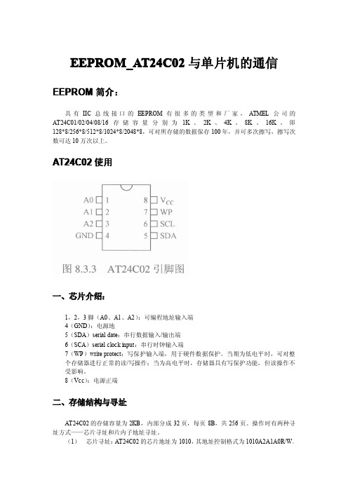
一、芯片介绍:
1,2,3 脚(A0 、A1 、A2 ) :可编程地址输入端 4(GND) :电源地 5(SDA)serial date:串行数据输入/输出端 6(SCA)serial clock input :串行时钟输入端 7(WP )write protect:写保护输入端,用于硬件数据保护。当期为低电平时,可对整 个存储器进行正常的读/写操作;当为高电平时,存储器具有写保护功能,但读操作不 受影响。 8(Vcc) :电源正端
}
二、存储结构与寻址
AT24C02 的存储容量为 2KB ,内部分成 32 页,每页 8B,共 256 页。操作时有两种寻芯片地址为 1010, 其地址控制格式为 1010A2A1A0R/W 。
其中 A2 、A1 、A0 为可编程地址选择位。A2 、A1、A0 引脚接高、低电平得到 确定的三位编码,与 1010 形成 7 位编码,即为该器件的地址码。R/W 位芯片 读写控制位,该位为 0,表示对芯片进行写操作;该位为 1,表示对芯片进行读 操作。 (2) 片内子地址寻址:芯片寻址可对内部 256B 中的任一个进行读/写操作,其寻址 范围为 00~FF,共 256 个寻址单位。
(2)指定地址连续读,此种方式的读地址控制与前面指定地址读相同,单片机接 收到每一个字节数据后应做出应答,只要 EEPROM 检测到应答信号,其内部的地址寄 存器就自动加 1,指向下一个单元,并顺序将指向的单元的数据送到 SDA 串行数据线 上。 当需要结束读操作时, 单片机接收到数据后在需要应答的时刻发送一个非应答信号, 接着再发送一个停止信号即可。这种读操作的数据帧格式如图 8.3.8 所示。
芯片操作时序图:对应后面的程序理解
总线时序图
串行EEPROM(24C02)接口方法讲解
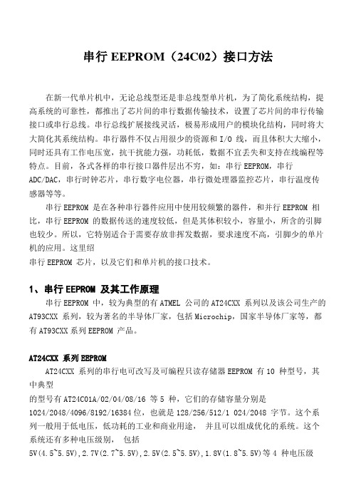
串行EEPROM(24C02)接口方法在新一代单片机中,无论总线型还是非总线型单片机,为了简化系统结构,提高系统的可靠性,都推出了芯片间的串行数据传输技术,设置了芯片间的串行传输接口或串行总线。
串行总线扩展接线灵活,极易形成用户的模块化结构,同时将大大简化其系统结构。
串行器件不仅占用很少的资源和I/O 线,而且体积大大缩小,同时还具有工作电压宽,抗干扰能力强,功耗低,数据不宜丢失和支持在线编程等特点。
目前,各式各样的串行接口器件层出不穷,如:串行EEPROM,串行ADC/DAC,串行时钟芯片,串行数字电位器,串行微处理器监控芯片,串行温度传感器等等。
串行EEPROM 是在各种串行器件应用中使用较频繁的器件,和并行EEPROM 相比,串行EEPROM 的数据传送的速度较低,但是其体积较小,容量小,所含的引脚也较少。
所以,它特别适合于需要存放非挥发数据,要求速度不高,引脚少的单片机的应用。
这里绍串行EEPROM 芯片,以及它们和单片机的接口技术。
1、串行EEPROM 及其工作原理串行EEPROM 中,较为典型的有ATMEL 公司的AT24CXX 系列以及该公司生产的AT93CXX 系列,较为著名的半导体厂家,包括Microchip,国家半导体厂家等,都有AT93CXX系列EEPROM 产品。
AT24CXX 系列EEPROMAT24CXX 系列的串行电可改写及可编程只读存储器EEPROM 有10 种型号,其中典型的型号有AT24C01A/02/04/08/16 等5 种,它们的存储容量分别是1024/2048/4096/8192/16384位,也就是128/256/512/1 024/2048 字节。
这个系列一般用于低电压,低功耗的工业和商业用途,并且可以组成优化的系统。
这个系统还有多种电压级别,包括5V(4.5~5.5V),2.7V(2.7~5.5V),2.5V(2.5~5.5V),1.8V(1.8~5.5V)等4 种电压级别。
I2C串行EEPROM系列中文资料

2005 Microchip Technology Inc.
DS21930A_CN 第 3 页
24AAXX/24LCXX/24FCXX
2.0 电气特性
绝对最大额定值 (†)
VCC.............................................................................................................................................................................6.5V 相对于 Vss 的所有输入和输出 ............................................................................................................ -0.6V 到 VCC +1.0V 存储温度 ................................................................................................................................................. -65°C 到 +150°C 环境温度 (使用电源时)........................................................................................................................ -40°C 到 +125°C 所有引脚静电保护 ....................................................................................................................................................................≥ 4 kV
常用EEPROM存储器
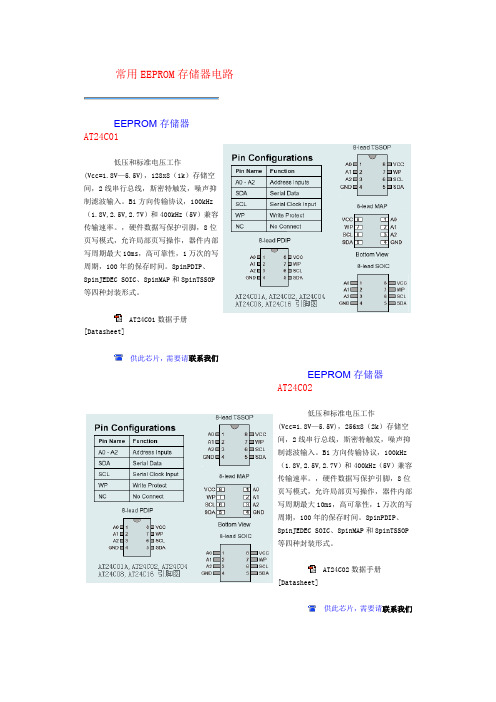
常用EEPROM存储器电路EEPROM存储器AT24C01低压和标准电压工作(Vcc=1.8V—5.5V),128x8(1k)存储空间,2线串行总线,斯密特触发,噪声抑制滤波输入。
Bi方向传输协议,100kHz (1.8V,2.5V,2.7V)和400kHz(5V)兼容传输速率。
,硬件数据写保护引脚,8位页写模式,允许局部页写操作,器件内部写周期最大10ms,高可靠性,1万次的写周期,100年的保存时间。
8pinPDIP、8pinJEDEC SOIC、8pinMAP和8pinTSSOP等四种封装形式。
AT24C01数据手册[Datasheet]供此芯片,需要请联系我们EEPROM存储器AT24C02低压和标准电压工作(Vcc=1.8V—5.5V),256x8(2k)存储空间,2线串行总线,斯密特触发,噪声抑制滤波输入。
Bi方向传输协议,100kHz (1.8V,2.5V,2.7V)和400kHz(5V)兼容传输速率。
,硬件数据写保护引脚,8位页写模式,允许局部页写操作,器件内部写周期最大10ms,高可靠性,1万次的写周期,100年的保存时间。
8pinPDIP、8pinJEDEC SOIC、8pinMAP和8pinTSSOP 等四种封装形式。
AT24C02数据手册[Datasheet]供此芯片,需要请联系我们EEPROM存储器AT24C04低压和标准电压工作(Vcc=1.8V—5.5V),512x8(4k)存储空间,2线串行总线,斯密特触发,噪声抑制滤波输入。
Bi方向传输协议,100kHz (1.8V,2.5V,2.7V)和400kHz(5V)兼容传输速率。
,硬件数据写保护引脚,8位页写模式,允许局部页写操作,器件内部写周期最大10ms,高可靠性,1万次的写周期,100年的保存时间。
8pinPDIP、8pinJEDEC SOIC、8pinMAP和8pinTSSOP 等四种封装形式。
AT24C04数据手册[Datasheet]供此芯片,需要请联系我们EEPROM存储器AT24C08低压和标准电压工作(Vcc=1.8V—5.5V),1024x8(8k)存储空间,2线串行总线,斯密特触发,噪声抑制滤波输入。
1AT93C46_56_55串行EEPROM及单片机程序
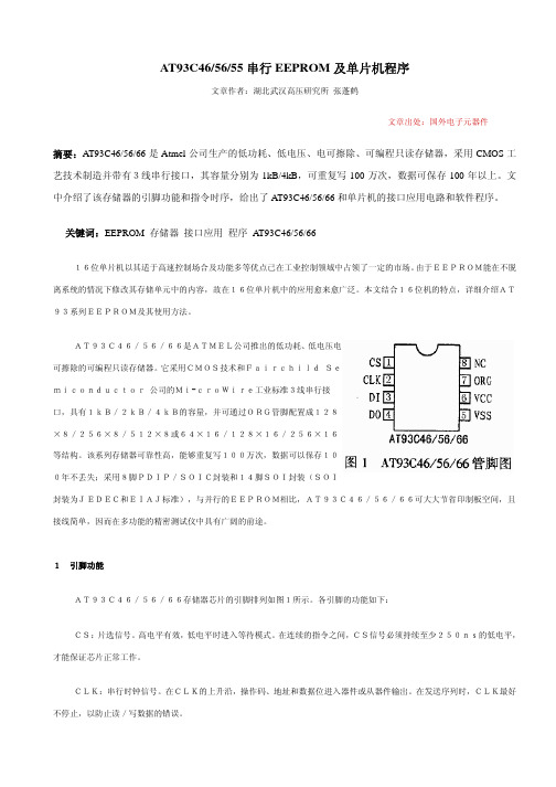
AT93C46/56/55串行EEPROM及单片机程序文章作者:湖北武汉高压研究所张蓬鹤文章出处:国外电子元器件摘要:AT93C46/56/66是Atmel公司生产的低功耗、低电压、电可擦除、可编程只读存储器,采用CMOS工艺技术制造并带有3线串行接口,其容量分别为1kB/4kB,可重复写100万次,数据可保存100年以上。
文中介绍了该存储器的引脚功能和指令时序,给出了AT93C46/56/66和单片机的接口应用电路和软件程序。
关键词:EEPROM 存储器接口应用程序 AT93C46/56/6616位单片机以其适于高速控制场合及功能多等优点已在工业控制领域中占领了一定的市场。
由于EEPROM能在不脱离系统的情况下修改其存储单元中的内容,故在16位单片机中的应用愈来愈广泛。
本文结合16位机的特点,详细介绍AT93系列EEPROM及其使用方法。
AT93C46/56/66是ATMEL公司推出的低功耗、低电压电可擦除的可编程只读存储器。
它采用CMOS技术和Fairchild Semiconductor 公司的Mi-croWire工业标准3线串行接口,具有1kB/2kB/4kB的容量,并可通过ORG管脚配置成128×8/256×8/512×8或64×16/128×16/256×16等结构。
该系列存储器可靠性高,能够重复写100万次,数据可以保存100年不丢失;采用8脚PDIP/SOIC封装和14脚SOI封装(SOI封装为JEDEC和EIAJ标准),与并行的EEPROM相比,AT93C46/56/66可大大节省印制板空间,且接线简单,因而在多功能的精密测试仪中具有广阔的前途。
1 引脚功能AT93C46/56/66存储器芯片的引脚排列如图1所示。
各引脚的功能如下:CS:片选信号。
高电平有效,低电平时进入等待模式。
在连续的指令之间,CS信号必须持续至少250ns的低电平,才能保证芯片正常工作。
- 1、下载文档前请自行甄别文档内容的完整性,平台不提供额外的编辑、内容补充、找答案等附加服务。
- 2、"仅部分预览"的文档,不可在线预览部分如存在完整性等问题,可反馈申请退款(可完整预览的文档不适用该条件!)。
- 3、如文档侵犯您的权益,请联系客服反馈,我们会尽快为您处理(人工客服工作时间:9:00-18:30)。
1Features•Serial Peripheral Interface (SPI) Compatible •Supports SPI Modes 0 (0,0) and 3 (1,1)•Low-voltage and Standard-voltage Operation –2.7 (V CC = 2.7V to 5.5V)• 3.0 MHz Clock Rate (5V) •8-byte Page Mode•Block Write Protection–Protect 1/4, 1/2, or Entire Array•Write Protect (WP) Pin and Write Disable Instructions for Both Hardware and Software Data Protection •Self-timed Write Cycle (10 ms max)•High Reliability–Endurance: One Million Write Cycles –Data Retention: 100 Years•Automotive Grade Devices Available•8-lead PDIP and 8-lead JEDEC SOIC PackagesDescriptionThe AT25010/020/040 provides 1024/2048/4096 bits of serial electrically erasable programmable read only memory (EEPROM) organized as 128/256/512 words of 8bits each. The device is optimized for use in many industrial and commercial applica-tions where low-power and low voltage operation are essential. The AT25010/020/040is available in space saving 8-lead PDIP and 8-lead JEDEC SOIC packages.The AT25010/020/040 is enabled through the Chip Select pin (CS) and accessed via a 3-wire interface consisting of Serial Data Input (SI), Serial Data Output (SO), and Serial Clock (SCK). All programming cycles are completely self-timed, and no sepa-rate ERASE cycle is required before WRITE.BLOCK WRITE protection is enabled by programming the status register with one of four blocks of write protection. Separate program enable and program disable instruc-tions are provided for additional data protection. Hardware data protection is provided via the WP pin to protect against inadvertent write attempts. The HOLD pin may be used to suspend any serial communication without resetting the serial sequence.Pin Configurations8-lead PDIP2AT25010/020/0400606M–SEEPR–06/03Block DiagramAbsolute Maximum Ratings*Operating Temperature.................................-55°C to + 125°C *NOTICE:Stresses beyond those listed under “Absolute Maximum Ratings” may cause permanent dam-age to the device. This is a stress rating only and functional operation of the device at these or any other conditions beyond those indicated in the operational sections of this specification is not implied. Exposure to absolute maximum rating conditions for extended periods may affect device reliability.Storage T emperature....................................-65°C to + 150°C Voltage on Any Pinwith Respect to Ground....................................-1.0V to + 7.0V Maximum Operating Voltage ..........................................6.25V DC Output Current........................................................5.0 mA3AT25010/020/0400606M–SEEPR–06/032.V IL min and V IH max are reference only and are not tested.Pin Capacitance (1)DC CharacteristicsApplicable over recommended operating range from: T AI = -40°C to +85°C, V CC = +2.7V to +5.5V, V CC = +2.7V to +5.5V (unless otherwise noted).4AT25010/020/0400606M–SEEPR–06/03AC CharacteristicsApplicable over recommended operating range from T AI = -40°C to +85°C, V CC = As Specified, CL = 1 TTL Gate and 100 pF (unless otherwise noted).5AT25010/020/0400606M–SEEPR–06/03Serial Interface DescriptionMASTER: The device that generates the serial clock.SLAVE: Because the Serial Clock pin (SCK) is always an input, the AT25010/020/040always operates as a slave.TRANSMITTER/RECEIVER: The AT25010/020/040 has separate pins designated for data transmission (SO) and reception (SI).MSB: The Most Significant Bit (MSB) is the first bit transmitted and received.SERIAL OP-CODE:received. This byte contains the op-code that defines the operations to be performed.The op-code also contains address bit A8 in both the READ and WRITE instructions.INVALID OP-CODE: If an invalid op-code is received, no data will be shifted into the AT25010/020/040, and the serial output pin (SO) will remain in a high impedance state communication.CHIP SELECT: device is not selected, data will not be accepted via the SI pin, and the serial output pin (SO) will remain in a high impedance state.HOLD: is used in conjunction with the AT25010/020/040. When the device is selected and a serial sequence is underway,while the SO pin is in the high impedance state.WRITE PROTECT:write operation.6AT25010/020/0400606M–SEEPR–06/03SPI Serial InterfaceFunctional DescriptionThe AT25010/020/040 is designed to interface directly with the synchronous serial peripheral interface (SPI) of the 6805 and 68HC11 series of microcontrollers.The AT25010/020/040 utilizes an 8-bit instruction register. The list of instructions and their operation codes are contained in Table 1. All instructions, addresses, and data are transferred with the MSB first and start with a high-to-low CS transition.Note:“A” represents MSB address bit A8.7AT25010/020/0400606M–SEEPR–06/03WRITE ENABLE (WREN): The device will power up in the write disable state when V CC is applied. All programming instructions must therefore be preceded by a Write Enable WRITE DISABLE (WRDI): To protect the device against inadvertent writes, the Write Disable instruction disables all programming modes. The WRDI instruction is indepen-READ STATUS REGISTER (RDSR): The Read Status Register instruction provides access to the status register. The READY/BUSY and Write Enable status of the device can be determined by the RDSR instruction. Similarly, the Block Write Protection bits indicate the extent of protection employed. These bits are set by using the WRSR instruction.WRITE STATUS REGISTER (WRSR): The WRSR instruction allows the user to select one of four levels of protection. The AT25010/020/040 is divided into four array seg-ments. Top quarter (1/4), Top half (1/2), or all of the memory segments can be protected. Any of the data within any selected segment will therefore be READ only. The block write protection levels and corresponding status register control bits are shown in Table 4.The two bits, BP1 and BP0 are nonvolatile cells that have the same properties and func-tions as the regular memory cells (e.g. WREN, t WC , RDSR).Table 3. Read Status Register Bit DefinitionTable 4. Block Write Protect Bits8AT25010/020/0400606M–SEEPR–06/03READ SEQUENCE (READ): Reading the AT25010/020/040 via the SO (Serial Output)the READ op-code (including A8) is transmitted via the SI line followed by the byte address to be read (A7-A0). Upon completion, any data on the SI line will be ignored.The data (D7-D0) at the specified address is then shifted out onto the SO line. If only READ sequence can be continued since the byte address is automatically incremented and data will continue to be shifted out. When the highest address is reached, the address counter will roll over to the lowest address allowing the entire memory to be read in one continuous READ cycle.WRITE SEQUENCE (WRITE): In order to program the AT25010/020/040, the Write First, the device must be write enabled via the Write Enable (WREN) Instruction. Then a Write (WRITE) Instruction may be executed. Also, the address of the memory loca-tion(s) to be programmed must be outside the protected address field location selected by the Block Write Protection Level. During an internal write cycle, all commands will be ignored except the RDSR instruction.select the device, the WRITE op-code (including A8) is transmitted via the SI line fol-lowed by the byte address (A7-A0) and the data (D7-D0) to be programmed.(LSB) data bit.The READY/BUSY status of the device can be determined by initiating a READ STA-TUS REGISTER (RDSR) Instruction. If Bit 0 = 1, the WRITE cycle is still in progress. If Bit 0 = 0, the WRITE cycle has ended. Only the READ STATUS REGISTER instruction is enabled during the WRITE programming cycle.The AT25010/020/040 is capable of an 8-byte PAGE WRITE operation. After each byte of data is received, the three low order address bits are internally incremented by one;the six high order bits of the address will remain constant. If more than 8 bytes of data are transmitted, the address counter will roll over and the previously written data will be overwritten. The AT25010/020/040 is automatically returned to the write disable state at the completion of a WRITE cycle.NOTE:brought high. A new CS falling edge is required to re-initiate the serial communication.9AT25010/020/0400606M–SEEPR–06/03Timing DiagramsSynchronous Data Timing (for mode 0)WREN TimingWRDI Timing10AT25010/020/0400606M–SEEPR–06/03RDSR TimingWRSR TimingREAD Timing11AT25010/020/0400606M–SEEPR–06/03WRITE TimingHOLD Timing12AT25010/020/0400606M–SEEPR–06/03AT25010 Ordering Information13AT25010/020/0400606M–SEEPR–06/03AT25020 Ordering Information14AT25010/020/0400606M–SEEPR–06/03AT25040 Ordering Information15AT25010/020/0400606M–SEEPR–06/03Packaging Information8P3 – PDIP16AT25010/020/0400606M–SEEPR–06/038S1 – JEDEC SOIC0606M–SEEPR–06/03xMDisclaimer: Atmel Corporation makes no warranty for the use of its products, other than those expressly contained in the Company’s standard warranty which is detailed in Atmel’s Terms and Conditions located on the Company’s web site. The Company assumes no responsibility for any errors which may appear in this document, reserves the right to change devices or specifications detailed herein at any time without notice, and does not make any commitment to update the information contained herein. No licenses to patents or other intellectual property of Atmel are granted by the Company in connection with the sale of Atmel products, expressly or by implication. Atmel’s products are not authorized for use as critical components in life support devices or systems.Atmel CorporationAtmel Operations2325 Orchard Parkway San Jose, CA 95131Tel: 1(408) 441-0311Fax: 1(408) 487-2600Regional HeadquartersEuropeAtmel SarlRoute des Arsenaux 41Case Postale 80CH-1705 Fribourg SwitzerlandTel: (41) 26-426-5555Fax: (41) 26-426-5500AsiaRoom 1219Chinachem Golden Plaza 77 Mody Road Tsimshatsui East Kowloon Hong KongTel: (852) 2721-9778Fax: (852) 2722-1369Japan9F, Tonetsu Shinkawa Bldg.1-24-8 ShinkawaChuo-ku, Tokyo 104-0033JapanTel: (81) 3-3523-3551Fax: (81) 3-3523-7581Memory2325 Orchard Parkway San Jose, CA 95131Tel: 1(408) 441-0311Fax: 1(408) 436-4314Microcontrollers2325 Orchard Parkway San Jose, CA 95131Tel: 1(408) 441-0311Fax: 1(408) 436-4314La Chantrerie BP 7060244306 Nantes Cedex 3, France Tel: (33) 2-40-18-18-18Fax: (33) 2-40-18-19-60ASIC/ASSP/Smart CardsZone Industrielle13106 Rousset Cedex, France Tel: (33) 4-42-53-60-00Fax: (33) 4-42-53-60-011150 East Cheyenne Mtn. Blvd.Colorado Springs, CO 80906Tel: 1(719) 576-3300Fax: 1(719) 540-1759Scottish Enterprise Technology Park Maxwell BuildingEast Kilbride G75 0QR, Scotland Tel: (44) 1355-803-000Fax: (44) 1355-242-743RF/AutomotiveTheresienstrasse 2Postfach 353574025 Heilbronn, Germany Tel: (49) 71-31-67-0Fax: (49) 71-31-67-23401150 East Cheyenne Mtn. Blvd.Colorado Springs, CO 80906Tel: 1(719) 576-3300Fax: 1(719) 540-1759Biometrics/Imaging/Hi-Rel MPU/High Speed Converters/RF DatacomAvenue de Rochepleine BP 12338521 Saint-Egreve Cedex, France Tel: (33) 4-76-58-30-00Fax: (33) 4-76-58-34-80e-mailliterature@Web Site© Atmel Corporation 2003. All rights reserved. Atmel ® and combinations thereof, are the registered trade-marks of Atmel Corporation or its subsidiaries. Other terms and product names may be the trademarks of oth-ers.。