S1K
INA114AP,INA114AU,INA114BP,INA114BU,INA114AU 1KE4,INA114BU 1K,INA114BU 1KE4, 规格书,Datasheet 资料

INA114
INA114
INA114
SBOS014
Precision INSTRUMENTATION AMPLIFIER
FEATURES
q LOW OFFSET VOLTAGE: 50µV max q LOW DRIFT: 0.25µV/°C max q LOW INPUT BIAS CURRENT: 2nA max q HIGH COMMON-MODE REJECTION:
®
INA114
2
芯天下--/
PIN CONFIGURATIONS
P Package
8-Pin DIP
Top View
RG 1 V–IN 2 V+IN 3
V– 4
8 RG 7 V+ 6 VO 5 Ref
U Package
NC 1 RG 2 NC 3 V–IN 4 V+IN 5 NC 6 V– 7 NC 8
VCM = ±10V, ∆RS = 1kΩ G=1 G = 10
G = 100 G = 1000
G = 1000, RS = 0Ω
G=1 G = 10 G = 100 G = 1000 G=1 G=1 G = 10 G = 100 G = 1000
IO = 5mA, TMIN to TMAX VS = ±11.4V, RL = 2kΩ VS = ±2.25V, RL = 2kΩ
25kΩ
25kΩ
A3
25kΩ
25kΩ
4 (7) V–
(SOIC)
Feedback
(12) DIP Connected Internally
6
(11)
VO
5 Ref
(10)
GSC24BC02资料
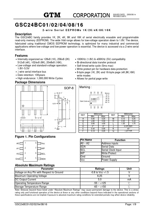
G S C 24B C 01/02/04/08/162-w i r e S e r i a l E E P R O M s 1K /2K /4K /8K /16KDescriptionThe GSC24BC family provides 1K, 2K, 4K, 8K and 16K of serial electrically erasable and programmable read-only memory (EEPROM). The wide Vdd range allows for low-voltage operation down to 1.8V. The device, fabricated using traditional CMOS EEPROM technology, is optimized for many industrial and commercial applications where low-voltage and low-power operation is essential. The device is accessed via a 2-wire serial interface.FeaturesInternally organized as 128x8 (1K), 256x8 (2K) 512x8 (4K), 1024x8 (8K), 2048x8 (16K), Low-voltage and standard-voltage operation: 1.8V~5.5V-wire serial interface bus Date retention: 100yearsHigh endurance: 1,000,000 Write Cycles 100KHz (1.8V) & 400KHz (5V) compatibilityBi-directional data transfer protocol Self-timed write cycle (5ms max)Write protect pin for hardware data protection8-byte page (1K, 2K) and 16-byte page (4K,8K,16K) write modesAllows for partial page writePackage DimensionsMillimeter Millimeter REF . Min. Max.REF . Min. Max.A 5.80 6.20 M 0.10 0.25B 4.80 5.00 H 0.35 0.49C 3.80 4.00 L 1.35 1.75D 0° 8° J 0.375 REF.E 0.40 0.90 K 45° F0.190.25G1.27 TYP .Figure 1. Pin ConfigurationsPin Name FunctionA0 – A2 Address inputs SDA Serial DataSCL Serial Clock Input WP Write Protect Gnd GroundVcc Power SupplyAbsolute Maximum RatingsParameterRatings Unit Voltage on Any Pin with Respect to Ground -0.8 to Vcc +1.5V Maximum Operating Voltage 6.25 V DC Output Current5.0 mA Operating Temperature Range -55 ~ +125 Storage Temperature Range-65 ~ +150Note: Stresses beyond those listed under “Absolute Maximum Ratings” may cause permanent damage to the device. This is a stress rating only and functional operation of the device at these or any other conditions beyond those indicated in the operational sections of these specifications are not implied. Exposure to absolute maximum rating conditions for extended periods may affect device reliability.Figure 2. Block DiagramPIN DescriptionsSerial Data (SDA): The SDA pin used for sending and receiving data bits in serial mode. Since the SDA pin is defined as an open-drain connection, a pull-up resistor is needed.Serial Clock (SCL): The SCL input is used to synchronize data input and output with the clocked out on the falling edge of SCL.Device/Page Addresses (A2, A1, A0): The A2, A1, and A0 pins are used to address multiple devices on a single bus system and should be hard-wired.The GSC24BC01 and GSC24BC02 use the A2, A1 and A0 pins to provide the capability for addressing up to eight 1K/2K devices on a single bus system (please see the Device Addressing section for further details)The GSC24BC04 uses the A2 and A1 inputs and a total of for 4K device may be addressed on a single bus system. The A0 pin in not used, but should be grounded if possible.The GSC24BC08 only uses the A2 input hardwire addressing. On a single bus system, a total of two 8K devices may be addressed. The A0 and A1 pins are not used, but should be grounded if possible.The GSC24BC16 does not uses the device address pins, so only one device can be connected to a single bus system. Therefore, the A0, A1 and A2 pins are not used, but should be grounded if possible.Write Protect (WP):The GSC24BC01/02/04/08/16 has a Write Protect pin that provides hardware data protection. When connected to ground, the Write Protect pin allows for normal read/write operations. If the WP pin is connected to V CC, no data can be overwritten.Memory OrganizationThe internal memory organization for the GSC24BC family is arranged differently for each of the densities. The GSC24bc01, for instance, is internally organized as 16 pages of 8 bytes each and requires a 7-bit data word address. The GSC24BC16, on the other hand, is organized as 128 pages of 16 bytes each with an 11-bit data word address. The table below summarizes these differences.Density # of pages Bytes per page Data word address lengthGSC24BC01 (1K) 16 pages 8 bytes 7 bitsGSC24BC02 (2K) 32 pages 8 bytes 8 bitsGSC24BC04 (4K) 32 pages 16 bytes 9 bitsGSC24BC08 (8K) 64 pages 16 bytes 10 bitsGSC24BC16 (16K) 128 pages 16 bytes 11 bitsPIN CapacitanceApplicable over recommended operating range from T A=25 , f=1.0MHz, Vcc=+1.8VSymbol Test Condition Max Unit ConditionC I/O Input/Output Capacitance (SDA) 8 pF V I/O=0VC IN Input Capacitance (A0, A1, A2, SCL) 6 pF V IN=0VNote: 1. This parameter is characterized and not 100% tested.DC CharacteristicsApplicable over recommended operating range from: T A=-40 ~ +85 , V CC=+1.8 ~ +5V (unless otherwise noted) Parameter Symbol Test Condition Min TYP Max Unit Supply Voltage V CC1 1.8 - 5.5 V Supply Voltage V CC2 2.7 - 5.5 V Supply Voltage V CC3 4.5 - 5.5 V Supply Current V CC=5.0V I CC READ at 100KHz - 0.4 1.0 mA Supply Current V CC=5.0V I CC WRITE at 100KHz - 2.0 3.0 mA Standby Current V CC=1.8V I SB1 V IN= V CC or V SS - 0.6 3.0 A Standby Current V CC=2.5V I SB2 V IN= V CC or V SS - 1.4 4.0 A Standby Current V CC=5.5V I SB3 V IN= V CC or V SS - 5.0 18 A Input Leakage Current I LI V IN= V CC or V SS - 0.2 5.0 A Output Leakage Current I LO V OUT= V CC or V SS- 0.1 5.0 A Input Low Level (1)V IL -0.6 - V CC x0.3 V Input High Level (1)V IH V CC x0.7 - V CC+0.5 V Output Low Level V CC=3.0V V OL2 I OL=2.1mA - - 0.4 V Output Low Level V CC=3.0V V OL1 I OL=0.15mA - - 0.2 V Note 1: V IL and V IH max are reference only and are not tested.ISSUED DATE :2006/06/14REVISED DATE :AC Characteristics Applicable over recommended operating range from: T A =-40 ~ +85 , V CC =+1.8 ~ 5.5V, C L =1 TTL Gate & 100pF (unless otherwise noted)Parameter Symbol Test Condition Min TYP Max UnitClock Frequency, SCL f SCL V CC =1.8V V CC =2.7 ~ 5.5V - - 100400KHzClock Pulse Width Low t LOWV CC =1.8VV CC =2.7 ~ 5.5V 4.7 1.2 - - s Clock Pulse Width High t HIGH V CC =1.8V V CC =2.7 ~ 5.5V 4.00.6 - - sNoise Suppression Time (1) t I V CC =1.8V V CC =2.7 ~ 5.5V- -10050 ns Clock Low to Data Out Valid t AAV CC =1.8VV CC =2.7 ~ 5.5V 0.1 0.1- 4.5 0.9 s Time the bus must be free before a new transmission can start (1) t BUF V CC =1.8VV CC =2.7 ~ 5.5V 4.7 1.2- - sStart Hold Time t HD.STAV CC =1.8V V CC =2.7 ~ 5.5V 4.00.6 - - s Start Setup Time t SU.STA V CC =1.8V V CC =2.7 ~ 5.5V 4.70.6- - sData in Hold Time t HD.DAT V CC =1.8VV CC =2.7 ~ 5.5V0 0 - - sData in Setup Time t US.DATV CC =1.8V V CC =2.7 ~ 5.5V 200100- - ns Input Rise Time (1) t RV CC =1.8VV CC =2.7 ~ 5.5V- - 1.0 0.3 s Input Fall Time (1) t F V CC =1.8VV CC =2.7 ~ 5.5V - - 300 300 nsStop Setup Time t SU.STOV CC =1.8V V CC =2.7 ~ 5.5V 4.70.6- - s Data Out Hold Time t DH V CC =1.8VV CC =2.7 ~ 5.5V100 50 - - nsWrite Cycle Time t WRV CC =1.8VV CC =2.7 ~ 5.5V - - 5 5ms 5.0V, 25 , Byte ModeEndurance (1) V CC =1.8V V CC =2.7 ~ 5.5V 1M 1M - - Write CyclesNote: 1. This parameter is characterized and not 100% tested.Device Operation Clock and Data Transitions: Transitions on the SDA pin should only occur when SCL is low (refer to the Data Validity timing diagram in Figure 5). If the SDA pin changes when SCL is high, then the transition will be interpreted as a START or STOP condition.START Condition: A START condition occurs when the SDA transitions form high to low when SCL is high. The START signal is usually used to initiate a command (refer to the Start and Stop Definition timing diagram in Figure 6).STOP Condition: A STOP condition occurs when the SDA transitions form low to high when SCL is high (refer to Figure 6. START and STOP Definition timing diagram). The STOP command will put the device into standby mode after no acknowledgment is issued during the read sequence.Acknowledge: An acknowledgement is sent by pulling the SDA low to confirm that a word has been successfully received. All addresses and data words are serially transmitted to and from the EEPROM in 8-bit words, so acknowledgments are usually issued during the 9th clock cycle.Standby Mode: Standby mode is entered when the chip is initially powered-on or after a STOP command has been issued and any internal operations have been completed. .Memory Reset: In the event of unexpected power or connection loss, a START condition can be issued to restart the input command sequence. If the device is currently in write cycle mode, this command will be ignored.BUS TIMINGFigure 3. SCL: Serial Clock, SDA: Serial Data I/OWRITE CYCLE TIMINGFigure 4. SCL: Serial Clock, SDA: Serial Data I/ONote: 1. The write cycle time t WR is the time from a valid stop condition of a write sequence to the end of the internal clear/write cycleFigure 5. DATA VALIDITYFigure 6. START & STOP DEFINITIONFigure 7. Output ACKNOWLEDGEDevice AddressingTo enable the chip for a read or write operation, an 8-bit device address word followed by a START condition must be issued. The 1st four bits of the device address word consists of a mandatory ‘1010’ pattern, while the 2nd four bits depend on the particular density being used (refer to Figure 8):In the 1K/2K chip, the next 3 bits should correspond to the hard-wired input A2, A1 and A0 device address bits.In the 4K chip, the next 3 bits are the A2 and A1 device address bits and a memory page address bit. The two device address bits must compare to their corresponding hard-wired input pins.In the 8K chip, the next 3 bits include the A2 device address bits with the next 2 bits used for memory page addressing. The A2 bit must compare to its corresponding hard-wired input pin.In the 16K chip does not use any device address bits but instead the 3 bits are used for memory page addressing.Figure 8. Device AddressThe memory page address bits, P2, P1 and P0 are used to select the page in the array. P2 represents the most significant bit, while P1 and P0 are considered the next most significant bits.The eight bit of the device address determines read or write operation. If the R/W bit is high, then a read operation is initiated. Otherwise, if the R/W bit is low, then a write operation is started.After comparing the device address and finding a match, the EEPROM device will issue an acknowledgment by pulling SDA low. If the comparison fails, the chip will return to standby mode.Figure 9. Byte WriteFigure 10. Page Write( * = DON’T CARE bit for 1K)Write OperationsByte/Page Write:If a write operation is entered (R/W=0) and an acknowledgment is sent, then the next sequence requires an 8-bit data word address. After an acknowledgment is received from this word address, the 1st byte of data can be loaded. The device will send an acknowledgment after each byte to confirm the transmission.To being the write cycle, a STOP condition must be issued (refer to Figure 9). Both byte and page write operations are supported, so the STOP condition can be issued after the 1st byte or the last byte in the page. When the STOP condition occurs, an internal time is started, all input are disabled, and the EEPROM will not respond to any more commands until the write cycle is completed.Note: The number of bytes in a page depends on the density used. If 1K density is used, then the page size is 8 bytes. In contrast, if the 16K density is used, then the page size is 16 bites. Refer to the Memory Organization section for more details.The internal page counter is incremented after each byte received, but the row location of the memory page will always remain the same. Therefore, the device will wrap around to the 1st byte in the page after the last byte in the page is received. Any further data loaded into the page buffer will overwrite the previous data loaded.Acknowledge Polling: After the STOP condition is issued, the write cycle begins. Acknowledge polling can be initiated by sending a START condition followed by the device address word. If the EEPROM has completed the internal write cycle and returned to standby mode, the device will respond by sending back an acknowledgment by pulling the SDA pin low. Otherwise, the sequence will be ignored and no acknowledgment will be sent.Read OperationsThere are three types of read operations: current address read, random address read, and sequence read. A random address read can be considered a current address read operation with an additional sequence in the beginning to load a different address into the internal counter. A sequential read occurs when subsequent bytes are clocked out after a current address read or random address read occurs.**ISSUED DATE :2006/06/14REVISED DATE :Current Address Read: A current address read operation is initiated by issuing R/W=1 in the device address word (refer to Figure 11). Since the internal address counter maintains the last address incremented by one accessed during the last read or write operation, the internal address counter will always retain the last address incremented by one.Random Read: To access a different address location that the one currently stored in the internal counter, a random read operation is provided. The random read is actually a combination of a “dummy” byte write sequence with a current address read command (refer to Figure 12). The “dummy” byte write loads a differentaddress into the internal counter, and the data can then be accessed using the current address read.Sequential Read: In order to access subsequent data word after a current address read or random read has been initiated, the user should send an acknowledgment to the EEPROM chip after each data byte received. If an acknowledgment is not received, then the chip will not send any more data and expect a STOP condition on the next cycle to reset back to standby more (refer to Figure 13).Sequential reads can be used to perform an entire chip read. Unlike the page write operation, the internal counter will increment to the next row after the last byte of the page has been reached. When the address reaches the last byte of the last memory page, the next address will increment to the 1st byte of the 1st memory page.Once the memory address limit is reached, the data word address will “roll over” and the sequential read will continue. When the microcontroller does not respond with a zero but does generate a following stop condition, the sequential read operations is terminated.Figure 11. Current Address ReadFigure 12. Random Read( * = DON’T CARE bit for 1K)Figure 13. Sequential Read*ISSUED DATE :2006/06/14REVISED DATE :GSC24BC Ordering InformationOrdering Code PackageOperating RangesGSC24BC01I GSC24BC02I GSC24BC04I GSC24BC08I GSC24BC16ISOP-8 Industrial (-40 ~ +85 )Product Ordering InformationGSC24BCXXYSC=SOP-8 G=GTM 24=Device Type Supply Voltage BC=1.8V to 5.5V Device Function 01= 1 Kbit (128x8) 02= 2 Kbit (256x8) 04= 4 Kbit (512x8) 08= 8 Kbit (1024x8) 16=16 Kbit (2048x8) Temperature I=Industrial (-40 ~ +85。
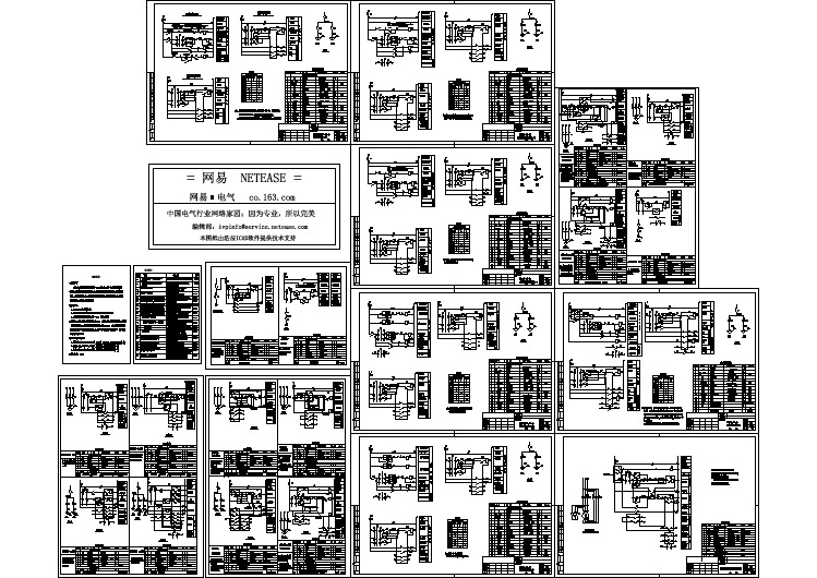
控制保护器控制风机和水泵图一用一备
数字电路触发器
S:置位(置1)端 R:复位(置0)端
两互补输出端
Q
Q
.
. 反馈线
& G1
& G2
两输入端 SD
RD
(二) 基本RS触发器
2. 逻辑功能
正常情况下, 两输出端旳状态 保持相反。一般 以Q端旳逻辑电 平表达触发器旳 状态,即Q=1, Q=0时,称为“1” 态;反之为“0” 态。
两互补输出端
发器状态不定。
3. 基本RS触发器应用电路:
(1) 无震颤开关电路
Q
Q
&&
5V
S
R
1k 1k
K
图4- 3 无震颤开关电路
机械开关在静止到新旳位置 之前其机械触头将要震颤几 次。图4-3电路能够处理震颤 问题。
设初始时K接R端,基本原 理如下:
a.K由右扳向左端,而且震颤几次,相当于RS=10
(或11)
1
K
1
&
0
G8 1
& G6
0
B
&
1
G4
& G2
Q
01
0
0
10
CP
设触发器原
& 01
G9
(a)
1
Rd
主从状 态一致
态为“0”
翻转为“1”态
态
(1)J=1, K=1
1
J
K
1 1
0
0
CP
设触发器原 态为“1”态
& G7
F主
& G8
Sd
A
1
Q’
& G5
& G3
Q’ F从
& G6 B
& G4
& G1
& G2
1.8叠合梁计算书

设 计梁截面
b= 800 h= 2500
第一次叠 合截面
在施 工过程中 梁下支撑 只考虑叠 合梁下部 h1高度内 荷载,上 部高度h2 的自重和 施工荷载
b= 800 h= 2500
钢筋 配筋 按原 设计 图。
,第
1300
二次 浇注
高度
第7页
1200
有第一次
浇注的h1
高度来承
受,故按
施工阶段
不加支撑
钢 筋应力 验算
在施 工阶段: 恒载标准 值G1k=
1/8× M1Gk= G1K×L2
= 2440
4520
KN
= 1.2 × 1.43 × 800 × 2440 + 0.9 × 360 × 6.7824
× 2440 = 8413.643136
> Vmax=
4520
KN
KZL29
51.4
KN /m
=
432.017
0.87 × 19292.2 × 1740
= 22.45083 N/mm2
因 M1Gk = 655.6646 <
0.35 M = 5607.35
M2k
12323846154
σs2k= 0.87Ash
01
= 0.87 × 19292.2 × 2940
= 250
M2k--在正常 使用阶段 的弯矩标 准值,查 弯设计矩 图:
12 @ 100
10
AsV
=
113.04 ×
10 = 11.304
s
100
按混凝土
结构设计
规范
7.5.4-2
式
Vc= 0.7ftbh01+1.25fy
Lecture 10-正交级数展开与波形检测
TE3221023 信号检测与估值 2012年春季
14
Lecture 10 -正交级数展开与波形检测
判决表达式
T T E xk H1 E xt f k t dt H1 E s1 (t ) nt f k t dt 0 0
P பைடு நூலகம்x1N | H j
考虑联合PDF
如果xk,k=1,…,N互不相关,则有
P x1N | H j P xk | H j
k 1
N
目标:正交级数展开得到的系数互不相关
TE3221023 信号检测与估值 2012年春季
3
Lecture 10 -正交级数展开与波形检测
完备的正交函数集
T 0
5
TE3221023 信号检测与估值 2012年春季
Lecture 10 -正交级数展开与波形检测
随机过程的正交级数展开
假设接收为信号
xt s t nt
其中s(t)是确知信号,n(t)是零均值的平稳随机过程,则 接收信号也是平稳随机过程。 由于随机过程是由很多样本函数构成的集合,而每个样 本函数是时间的函数,所以对给定的样本函数,可以进 行正交级数展开
x t
随机信号正交级 数展开
x1 , x2 ,..., xN
离散信号统 计检测
lx d
N 1
l x(t ) c
匹配滤波器
TE3221023 信号检测与估值 2012年春季
2
Lecture 10 -正交级数展开与波形检测
Problem Formulation
9
Lecture 10 -正交级数展开与波形检测
博弈论---混合战略纳什均衡

义为:
n
vi ( i , i ) ( j (s j ))ui (s) sS j1
n个参与人的混合战略纳什均衡
让我们以两人博弈为例说明这一点。假定S1 (s11, , s1K ) ,
即参S2与人(s12有1 ,K 个, s2纯J )战略,参与人2有J个纯战略。若参与人1相
1k
2 j u1 ( s1k , s2 j )
1k 2 j u1 ( s1k , s2 j )
K 1
j 1
K 1 j1
这里,1k 2 j 是参与人1选择 s1k 且参与人2选择 s2 j 的概率,即纯 战略组合 (s1k , s2 j )发生的概率。
n个参与人的混合战略纳什均衡
混合战略纳什均衡
用上述方法:求该猜谜游 戏的混合战略纳什均衡
正面 反面
正面
1 -1,
-1 1,
反面
-1 1,
1 -1,
如何理解混合战略 ——虚张声势
一个参与人选择混合战略的目的是给其 他参与人造成不确定性,这样尽管其他 参与人知道他选择某个特定纯战略的概 率是多少,但不知道实际上对手会采用 哪个战略。正是因为它在几个战略之间 的无差异性,他的行为才难以预测,混 合战略均衡才会出现。
小猪
大猪
按 等待
按 5,1 9,-1
等待 4,4 0,0
正面
1
正面 -1,
反面
-1 1,
-1
反面 1,
1 -1,
混合战略纳什均衡
在n个参与人博弈的战略式表述 G S1,, Sn;u1,,un
中,假定参与人 i 有K个纯战略:Si Si1, , Sik ,那么,
与人关心的是其期望效用。 最优混合战略:是指使期望效用函数最大的混合
S1K资料
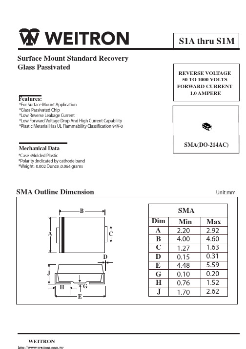
FIG.2 Maximum Non-Pepetitive Surge Current
10
1000
INSTANTANEOUS FORWARD CURRENT, (A)
INSTANTANEOUS REVERSE CURRENT, (uA)
100
TJ = 125 C
1.0
10
TJ = 25 C
1.0
TJ = 25 C
Symbol S1A S1B VRRM VRMS VDC IF(AV) 50 35 50 100 70 100
S1D S1G S1J S1K S1M Unit
200 140 200 400 280 400 1.0 600 420 600 800 1000 560 800 700 1000
V V V A
0.1
0.1
PULSEWIDTH:300us
.01 0 0.2 0.4 0.6 0.8 1.0 1.2 1.4 1.6 1.8
0.01 0 20 40 60 80 100 120 140
INSTANTANEOUS FORWARD VOLTAGE, (VOLTS)
PERCENT OF RATED PEAK REVERSE VOLTAGE, (%)
Mechanical Data
*Case : Molded Plastic *Polarity :Indicated by cathode band *Weight : 0.002 Ounce ,0.064 grams
SMA(DO-214AC)
SMA Outline Dimension
B
Unit:mm
元器件交易网
S1A thru S1M
Surface Mount Standard Recovery Glass Passivated
二极管代码S1K
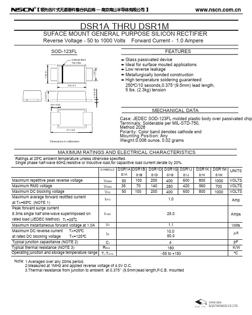
SUFACE MOUNT GENERAL PURPOSE SILICON RECTIFIERReverse Voltage - 50 to 1000 Volts Forward Current - 1.0 AmpereCase : JEDEC SOD-123FL molded plastic body over passivated chip Terminals : S olderable per MIL-STD-750,Method 2026Polarity : Color band denotes cathode end Mounting Position : AnyWeight :0.006 ounce, 0.02 gramsGlass passivated deviceIdeal for surface mouted applications FEATURESMECHANICAL DATAMAXIMUM RATINGS AND ELECTRICAL CHARACTERISTICSMetallurgically bonded constructionHigh temperature soldering guaranteed:250 C/10 seconds,0.375”(9.5mm) lead length,5 lbs. (2.3kg) tensionLow reverse leakageNote: 3.Thermal resistance from junction to ambient at 0.375” (9.5mm)lead length,P.C.B. mountedELECTRONICS CO.,LTD.LING JIESTAR SEARatings at 25 C ambient temperature unless otherwise specified.Single phase half-wave 60Hz,resistive or inductive load,for capacitive load current derate by 20%.DSR1A THRU DSR1M2.Measured at 1MHz and applied reverse voltage of 4.0V D.C.1.Averaged over any 20ms period.DSR1B SYMBOLS10070100400280400200140200600420600800560800V RRM V RMS V DC I (AV)I FSM V F 1.025.01.1Operating junction and storage temperature rangeMaximum repetitive peak reverse voltage Maximum RMS voltageMaximum DC blocking voltageMaximum average forward rectified current at T A =65 C (NOTE 1)Peak forward surge current8.3ms single half sine-wave superimposed on rated load (JEDEC Method)Maximum instantaneous forward voltage at 1.0A Maximum DC reverse current T A =25 C at rated DC blocking voltage T A =125 C Typical junction capacitance (NOTE 2)I R 10.050.0R θJA C J T J ,T STG1804-55 to +150Typical thermal resistance (NOTE 3)UNITSVOLTS VOLTS VOLTS AmpAmps Volts pF CA µK/W DSR1D DSR1G DSR1JDSR1K S1BS1DS1GS1JS1KT L =25 C503550S1ADSR1A 10007001000DSR1M S1MSOD-123FLDimensions in millimetersRATINGS AND CHARACTERISTIC CURVES DSR1A THRU DSR1MELECTRONICS CO.,LTD.LING JIESTAR SEAm A M P E R E SC A P A C I T A N C E , p FFIG.1 --TY PIC A L FOR WA R D C H A R A C TE R ISTIC FIG.2 -- TY PIC A L JU N C TION C APA C ITA N C EIN ST AN T AN EO U S FOR WAR D VOLT AG E,mV R EVER SE VOLT AGE,VOLT SI N S T A N T A N E O U S F O R W A R D C U R R E N T100100060070080090010001100510152025303540109876543210 µA M P E R E SA V E R A G E F O R W A R D C U R R E N T ,A M P E R E SI N S T A N T A N E O U S R E V E R S E C U R R E N TFIG.3 -- TYPICAL INSTANTANEOUS FIG.4 -- FOR WA R D D E R A TIN G C U R VEAMBIEN T T EMPER AT U R E,INSTANTANEOUS REVERSE VOLTAGE,V10100REVERSE CHARACTERISTICS1.00.80.60.40.20 25 50 75 100 125 150 175【领先的片式无源器件整合供应商—南京南山半导体有限公司】 |样品申请单模板第2页共2页。
二极管丝印S1G

SUFACE MOUNT GENERAL PURPOSE SILICON RECTIFIERReverse Voltage - 50 to 1000 Volts Forward Current - 1.0 AmpereCase : JEDEC SOD-123FL molded plastic body over passivated chip Terminals : S olderable per MIL-STD-750,Method 2026Polarity : Color band denotes cathode end Mounting Position : AnyWeight :0.006 ounce, 0.02 gramsGlass passivated deviceIdeal for surface mouted applications FEATURESMECHANICAL DATAMAXIMUM RATINGS AND ELECTRICAL CHARACTERISTICSMetallurgically bonded constructionHigh temperature soldering guaranteed:250 C/10 seconds,0.375”(9.5mm) lead length,5 lbs. (2.3kg) tensionLow reverse leakageNote: 3.Thermal resistance from junction to ambient at 0.375” (9.5mm)lead length,P.C.B. mountedELECTRONICS CO.,LTD.LING JIESTAR SEARatings at 25 C ambient temperature unless otherwise specified.Single phase half-wave 60Hz,resistive or inductive load,for capacitive load current derate by 20%.DSR1A THRU DSR1M2.Measured at 1MHz and applied reverse voltage of 4.0V D.C.1.Averaged over any 20ms period.DSR1B SYMBOLS10070100400280400200140200600420600800560800V RRM V RMS V DC I (AV)I FSM V F 1.025.01.1Operating junction and storage temperature rangeMaximum repetitive peak reverse voltage Maximum RMS voltageMaximum DC blocking voltageMaximum average forward rectified current at T A =65 C (NOTE 1)Peak forward surge current8.3ms single half sine-wave superimposed on rated load (JEDEC Method)Maximum instantaneous forward voltage at 1.0A Maximum DC reverse current T A =25 C at rated DC blocking voltage T A =125 C Typical junction capacitance (NOTE 2)I R 10.050.0R θJA C J T J ,T STG1804-55 to +150Typical thermal resistance (NOTE 3)UNITSVOLTS VOLTS VOLTS AmpAmps Volts pF CA µK/W DSR1D DSR1G DSR1JDSR1K S1BS1DS1GS1JS1KT L =25 C503550S1ADSR1A 10007001000DSR1M S1MSOD-123FLDimensions in millimetersRATINGS AND CHARACTERISTIC CURVES DSR1A THRU DSR1MELECTRONICS CO.,LTD.LING JIESTAR SEAm A M P E R E SC A P A C I T A N C E , p FFIG.1 --TY PIC A L FOR WA R D C H A R A C TE R ISTIC FIG.2 -- TY PIC A L JU N C TION C APA C ITA N C EIN ST AN T AN EO U S FOR WAR D VOLT AG E,mV R EVER SE VOLT AGE,VOLT SI N S T A N T A N E O U S F O R W A R D C U R R E N T100100060070080090010001100510152025303540109876543210 µA M P E R E SA V E R A G E F O R W A R D C U R R E N T ,A M P E R E SI N S T A N T A N E O U S R E V E R S E C U R R E N TFIG.3 -- TYPICAL INSTANTANEOUS FIG.4 -- FOR WA R D D E R A TIN G C U R VEAMBIEN T T EMPER AT U R E,INSTANTANEOUS REVERSE VOLTAGE,V10100REVERSE CHARACTERISTICS1.00.80.60.40.20 25 50 75 100 125 150 175【领先的片式无源器件整合供应商—南京南山半导体有限公司】 |样品申请单模板第2页共2页。
信号检测与估计理论 (复习题解)

例题解答
其中, 观测噪声 n服从对称三角分布, 如图3.1(a )所示。 若似然比检测门限 1, 求最佳判决式, 图示判决域, 计算P( H1 | H 0 )。 解:信号模型如图 3.1(b)所示。
p ( n)
1/ 2
p( x | H 0 )
1/ 2
p( x | H1 ) R1
2
0
图3.1(a )
第2章 信号检测与估计理论的基础知识 内容提要
三. 离散随机信号的函数
1. 一维雅可比变换, 特别是简单线性函数时 的变换。 2. N维雅可比变换。
四. 连续随机信号
1. 任意tk时刻采样所得样本 x(tk ) ( xk;tk )(k 1,2,, N )的概率密度 函数描述。 2. 统计平均量:均值, 均方值, 方差, 自相关函数, 协方差函数及关系。 3.平稳性:分类, 定义;重点是广义平稳 随机信号 : x ,rx( )。 4. 连续随机信号的互不相 关性和相互统计独立性 及关系。 5. 平稳连续随机信号的功 率谱密度 :
信号检测与估计理论
内容提要 例题解答
第 1章
信号检测与估计概论
内容提要
信号的随机性及其统计 处理方法 。
第 1章
略
信号检测与估计概论
例题解答
第2章 信号检测与估计理论的基础知识 内容提要
一. 离散随机信号
1. 概率密度函数 p( x)及特性: 非负, 全域积分等于1, 落入[a,b]间的概率 。 2. 统计平均量:均值, 方差。 3. 高斯离散随机信号的概 率密度函数及特 点:x ~ N( x , x2 )。
a cos(t )d 0 2 信号的自相关函数rx (t j , tk ) Ea cos(t j )a cos(tk )
国际基本单位

量的名称 单位名称 单位符号
长度 米
m
质量
千克(公 kg 斤)
时间 秒
s
电流 安培 A
热力学温 开尔文 K 度
物质的量 摩尔 mol
发光强度 坎德拉 cd
量的名称 单位名称 单位符号 其它表示 实例
频率 赫兹 Hz
s-1
力;重力 牛顿 N
kg·m/s2
压力,压 帕斯卡 Pa 强;应力
长 度 海里
n mile
1 n mile =1 852m (只 用于航 程)
速 度 节
kn
1 kn=1
n mile/
=(1 852/3
600) m/s (只用于 航程)
质 量 吨
t
1 t= 1000kg
质 量
体 积 能
级 差 线密度
原子 u 质量单位
升
L,(l)
电子伏 eV
分贝 dB 特[克斯] tex
1 u≈ 1.660 565 5× 10-27kg 1 L= 1dm= 10-3m3 1 eV≈ 1.602 189 2× 10-19J
1 tex=1 g/km
cd·sr
光照度 勒克斯 lx 放射性活 贝可勒尔 Bq 度
吸收剂量 戈瑞 Gy 剂量当量 希沃特 Sv
lm/m2 s-1
J/kg J/kg
量的名称 单位名称 单位符号 换算关系 和说明
时 间 分
min
1 min=
60 s
[小] h 时
1 h =60 min =3 600
s
天 d (日)
国际单位制的基本单位量的名称单位名称单位符号量的名称单位名称单位符号长度米mkg频率赫兹hzns1kgms2质量力重力牛顿时间秒s帕斯卡panm2电流安培a焦尔jnm开尔文k瓦特wjs物质的量摩尔mol电荷量库仑cas发光强度坎德拉cd伏特vwa电容法拉fcv电阻欧姆va电导西门子swbavvs磁通量韦伯特斯拉twbm2电感享利hwba其它表示实例千克公斤压力压强应力能量功热量热力学温度功率辐射通量电位电压电动势磁通量密度磁感应强度摄氏温度摄氏度光通量流明lmcdsr光照度放射性活度勒克斯贝可勒尔bqlxlmm2s1jkgjkg吸收剂量戈瑞gysv剂量当量希沃特量的名称单位名称单位符号时间分minh平面角度旋转速度转每分rmin长度海里nmile速度节kn质量吨t换算关系和说明1min60s1h60min3600s1d24h86400s1648000rad为圆周率16010800rad1601801rmin160s11nmile1852m只用于航程1kn1nmileh18523600ms只用于航程1t1000kg小时天日角秒d角分原子质量单位u1u166056551027kg体积升能电子伏ev级差线密度分贝特克斯dbtexll1l1dm103m31ev160218921019j1tex1gkm
西南天山下志留统柯坪塔格组(S1k)沉积环境分析

西南天山下志留统柯坪塔格组(S1k)沉积环境分析李培树梁东赵德怀吴浩王海鸿(中国冶金地质总局新疆地质勘查院乌鲁木齐83000)摘要下志留统柯坪塔格组(S1k)是西南天山广泛分布的地层,本文通过对柯坪塔格组地层划分沿革、剖面特征、顶底界线特征、基本层序特征、物源区构造背景、碎屑岩的粒度特征等进行研究分析,认为本组砂岩成分来源于构造活动较强的区域,可能来源于北部南天山早古生代俯冲碰撞造山带,碎屑岩沉积时物源既有大陆岛弧环境又有大洋岛弧及大陆边缘环境,沉积时物质来源具有多源性的特征,但主要来自沉积岩区;柯坪塔格组上段其沉积环境为浅海滨岸-陆棚环境,下段是较为封闭或半封闭并且氧化环境下的沉积,为潮坪沉积环境。
柯坪塔格组沉积环境由潮坪相向浅海滨岸-陆棚相转化,说明海水深度由浅到深,海平面上升。
关键词柯坪塔格组层序特征粒度特征沉积环境西南天山0引言下志留统柯坪塔格组分布于西南天山喀尔塔格-喀拉乔喀-乌塘库勒套南麓、南中部喀什噶尔山-克孜塔依-也台库勒-开勒品塔格一带及库木塔格幅琼布拉克乔喀北麓一带,呈近东西向、北东-南西向展布。
区域上成矿作用以沉积成矿为主,较为重要的是伽师铜矿、察尔其铜矿,均为沉积成因的砂岩型铜矿。
作为区域上重要的地质体,研究柯坪塔格组沉积环境,对区域铜矿床形成的沉积环境具有重要的参考意义。
1地层划分沿革张日东(1959)在《新疆天山南麓古生代地层》里介绍,西尼村(1943-1945)创名柯坪塔格岩系,创名地柯坪塔格地区。
地质部十三大队(1956)在柯坪地区进行1:20万区域地质调查,将一套以绿色为主的一套碎屑岩系划为柯坪塔格岩系;新疆科学分院詹士高(1964)在柯坪地区进行专题地层研究,在该组中采到大量笔石,时代改为早志留世称柯坪塔格组。
新疆区测队乔新东、张太荣(1973),西北石油局(1985)分别在该区内进行专题地层研究,结论与詹士高所提交成果基本相同。
《西北地区区域地层表·新疆维吾尔自治区分册》、《新疆古生界》、《新疆维吾尔自治区区域地质志》及《新疆维吾尔自治区岩石地层》(1999)均沿用柯坪塔格组。
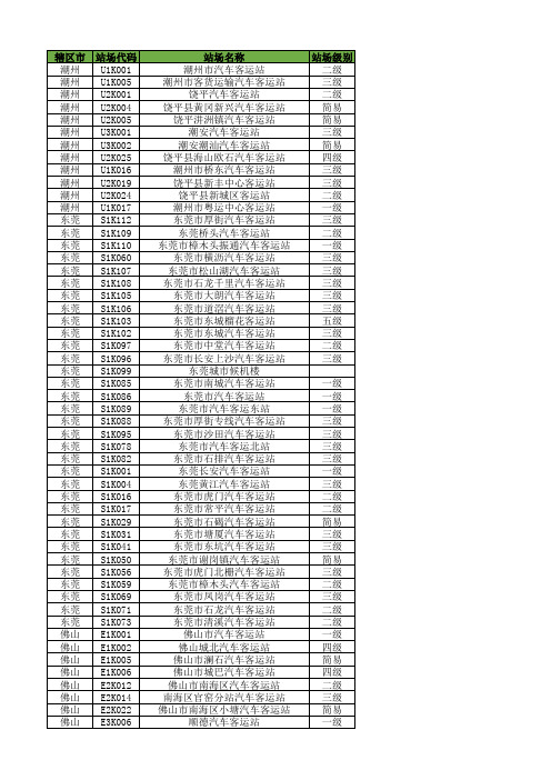
广东省班线客运-客运站信息
番禺汽车客运站
四级 三级 三级 三级 简易 简易 二级 一级 二级 简易 二级 三级 简易 三级 二级 五级
一级
一级 二级 简易 简易 二级 一级
三级
一级 一级 三级 简易
简易
简易
简易 二级 五级 简易 三级 一级
三级 三级 一级
广州
广州 广州 广州 广州 广州 广州
辖区市 潮州 潮州 潮州 潮州 潮州 潮州 潮州 潮州 潮州 潮州 潮州 潮州 东莞 东莞 东莞 东莞 东莞 东莞 东莞 东莞 东莞 东莞 东莞 东莞 东莞 东莞 东莞 东莞 东莞 东莞 东莞 东莞 东莞 东莞 东莞 东莞 东莞 东莞 东莞 东莞 东莞 东莞 东莞 东莞 东莞 佛山 佛山 佛山 佛山 佛山 佛山 佛山 佛山
站场名称 潮州市汽车客运站 潮州市客货运输汽车客运站 饶平汽车客运站 饶平县黄冈新兴汽车客运站 饶平汫洲镇汽车客运站 潮安汽车客运站 潮安潮汕汽车客运站 饶平县海山欧石汽车客运站 潮州市桥东汽车客运站 饶平县新丰中心客运站 饶平县新城区客运站 潮州市粤运中心客运站 东莞市厚街汽车客运站 东莞桥头汽车客运站 东莞市樟木头振通汽车客运站 东莞市横沥汽车客运站 东莞市松山湖汽车客运站 东莞市石龙千里汽车客运站 东莞市大朗汽车客运站 东莞市道滘汽车客运站 东莞市东城榴花客运站 东莞市东城汽车客运站 东莞市中堂汽车客运站 东莞市长安上沙汽车客运站 东莞城市候机楼 东莞市南城汽车客运站 东莞市汽车客运站 东莞市汽车客运东站 东莞市厚街专线汽车客运站 东莞市沙田汽车客运站 东莞市汽车客运北站 东莞市石排汽车客运站 东莞长安汽车客运站 东莞黄江汽车客运站 东莞市虎门汽车客运站 东莞市常平汽车客运站 东莞市石碣汽车客运站 东莞市塘厦汽车客运站 东莞市东坑汽车客运站 东莞市谢岗镇汽车客运站 东莞市虎门北栅汽车客运站 东莞市樟木头汽车客运站 东莞市凤岗汽车客运站 东莞市石龙汽车客运站 东莞市清溪汽车客运站 佛山市汽车客运站 佛山城北汽车客运站 佛山市澜石汽车客运站 佛山市城巴汽车客运站 佛山市南海区汽车客运站 南海区官窑分站汽车客运站 佛山市南海区小塘汽车客运站 顺德汽车客运站
最小错误概率准则

P(H0)
yB
f
( y / H0 )dy
P(H1)
yB
f
(y/
H1)dy
第6章 数字信号的最佳接收
其中
B
f ( yB / H1) f (yB / H0)
P(H 0 ) P(H1)
0
(6-20)
最小错误概率准则应写为
(y)
f f
(Y (Y
/ H1) / H0)
第6章 数字信号的最佳接收
设在发送端发射机之后产生的二元信号为s0(t)和s1(t),它 们为持续时间T的确知基带信号或频带信号。信号通过信道 传输时,假定混入了加性噪声n(t),在接收端收到的信号y(t) 应该是信号和噪声之和。
我们用H0和H1分别表示零假设和备择假设,其意义分 别表示s0(t)和s1(t)信号的存在,先验概率分别为P(H0)和 P(H1)。假设为H0时,接收信号为
lim
t0
s12k
t
N
1 n0
T 0
s12
(t)dt
N
lim
t0 N
k 1
s02k
2
2 n
1 n0
lim
t0
s02k
t
N
1 n0
T 0
s02
(t)dt
第6章 数字信号的最佳接收
将其代入式(6-24)并按式(6-22)取对数后可写为
ln (x) 2 n0
D1
D0
P(H 0 ) P(H1)
0
(6-21)
D1
ln ( y) ln 0
(6-22)
差分密码分析和线性密码分析原理

2轮DES的特征差分密码分析
所以, 在第2轮后,所有S盒都得到差分输
入0,产生的差分输出也是0; f(R,K)的输出在2轮后是0,差分输出则是 (00 00 00 00 , 60 00 00 00)
22
2轮DES的特征差分密码分析
假定:去掉初始置换IP和最终置换FP。2轮的差分分析
共有7个步骤。
18
2轮DES的特征差分密码分析
19
2轮DES的特征差分密码分析
在第一轮中,输入到函数f的差分结果是 a’= 60 00 00 00
经f 中的扩展变换后, 把这部分放进了每个S盒的中间4
个比特,顺序是
S1:6 = 0110 S2:0 = 0000 S3, . . . , S8 等等
因为所有边缘比特都是0,所以S1是唯一的得到非0差分
• 线性分析的分析者利用了包含明文、密文和子密钥的线性表达式 发生的较大可能性 。
线性密码分析的基本方法
随机给定的明文P和相应的密文C上面的等 式成立的概率p≠1/2
线性密码分析的基本方法——相关定理
线性密码分析的基本方法
用堆积引理, 我们可以将每轮变换中偏差最大的线性逼近式进 行组合, 组合后的所有轮变换的线性逼近式, 也将拥有最佳的偏 差, 即寻找分组密码的最佳线性逼近式.
S1 的差分分布表
0 . . . . . . . . . 63 =26-1
后面的行:
6比例特如的,差当分输x’入=x’01有时64, 个6个可
值能:的00-y3’F(中16进有制5个,值10进:0,制1,是2, 4, 8
0-63考) 虑输入异或值为34时,
呈现0可能次数,就是说不出
4比可特的能差的分输输出出异y’或有是1:6个
- 1、下载文档前请自行甄别文档内容的完整性,平台不提供额外的编辑、内容补充、找答案等附加服务。
- 2、"仅部分预览"的文档,不可在线预览部分如存在完整性等问题,可反馈申请退款(可完整预览的文档不适用该条件!)。
- 3、如文档侵犯您的权益,请联系客服反馈,我们会尽快为您处理(人工客服工作时间:9:00-18:30)。
ride-rode
riding What was he doing when the UFO arrived ? He was …when the UFO ….
People are talking about the UFO with the reporter.
Where were you when the UFO arrived?
What were they doing when the UFO arrived?
They were cooking dinner.
What was he doing when the UFO arrived ?
He was getting out of the shower when the UFO arrived.
c was in the kitchen. 4.__I e was in my barber shop. 5.__I I was cooking dinner.
I was cutting hair.
f I was in the barber’s chair. I was sitting on/in the chair. 6.__
Henry’s father
Henry’s grandmother
Henry’s grandfather
Henry’s … was in the … when ET arrived.
He/She was … in the … when ET arrived.
Henry’s uncle
barber
I was doing homework at six last night.
Unit 3 What were you doing when the UFO arrived?
UFO 不明飞行物;飞碟
Do you know?
What is UFO?
UFO---”Unidentified Flying Object”
a barber shop cutting hair
… was … in the barber shop when ET arrived.
What were other people on the earth(地球) doing when the UFO arrived?
landed(着陆)
What was he doing when the UFO arrived?
get out 出去;离开 get out of 从… 出来get out of the shower 洗完澡出来 talk on the phone 通过电话交谈 cut 剪;切;割
Unit3
What were you doing when the UFO arrived?
the UFO
ET’s trip to the earth
living room
bedroom
kitchen
batWhere were Henry’s family when ET arrived? What were Henry’s family doing when ET arrived?
d b a c e f
What were you doing?
1.__I d was in the bathroom.
b was in my bedroom. 2.__I
I was getting out of the shower.
I was sleeping late.
a was in front of the library. I was borrowing some books. 3.__I
昨天这个时候
I was having a Chinese class.
I was reading. I was listening carefully. I was playing with my classmates. I was ……
过去进行时
含义: 表示过去某个时刻正在进行的动作。
结构: be (was/were) + doing 例句:What were you doing at six last night?
She was watching TV in the living room when ET arrived.
Henry’s mother was in the living room.
ET
He was sleeping in the bedroom when ET arrived.
ET
Henry’s brother was in the bedroom.
UFO
Unidentified Flying Object
Do you believe (相信) the UFO? What do you know about the UFO?
2005年11月22日10:23,不明飞行物飞 广州上空 市民拍下UFO画面
Henry
ET
an alien
1a. Match the statements with the people in the pictures.
1b. listening
• a. standing in front of the library/ studying in the library • b. cleaning my room/ sleeping late • c. making a milk shake/ cooking dinner • d. getting out of the shower/ • talking on the phone • e. eating lunch/ cutting hair
• Free talk
• • • • Where are you now? We are in the classroom now. What are you doing now? We are having an English class.
• What were you doing at this time yesterday?
He was playing football.
What was she doing when the UFO arrived?
She was sleeping.
What was he doing when the UFO arrived?
He was talking on the phone.
UFO:Unidentified Flying Object 不明飞行物
•
1947年6月24日,一名叫做阿诺 德的美国商人,架着一架小型飞机 在华盛顿州上空,发现一组巨型不 明飞行物以1000公里左右的速度, 同他一起在空中翱翔。阿诺德的有 关目击报告第一次引起公众的兴趣, 从此“飞碟”或UFO便迅速流传开 来。
