RF_power_amplifier
射频模拟电路答案
射频模拟电路答案【篇一:02如何快速入门电子技术】>作者:刘昆山众所周知,学习讲究方法,方法对了,事半功倍,越学越有味。
方法不对,耗时耗力,困难重重,且可能随时让你产生放弃的念头。
万事开头难,同样,学电子技术的关键在于入门,故电子初学者首先要解决的就是如何快速入门的问题。
针对此,本人在这里做一个简单的阐述。
学习电子技术必须注重“理论+实践”的方法。
如果只学理论知识而不动手操作,则收效甚微;如果只进行实践操作而不学习理论知识,效果也不明显。
因此,学好电子技术必须做到理论、实践同时学,即既进行理论知识的学习又进行实践动手能力的充分锻炼。
一、如何快速学理论知识很多电子初学者最头痛的一件事,就是学理论知识,有些朋友索性就避开理论不学。
可要知道,不学理论而只动手操作,就像“无源之水”、“无本之木”,是很难真正掌握电子技术。
要学好电子技术,必须学好电子基础理论知识。
看书是最基本的学习方法,但是看书往往费时费脑,且不容易入门。
请身边的朋友帮忙指点下,朋友不一定会倾其全心,即使想倾其全心,也不一定能倾其全力,因为他不一定有时间。
下面推荐四部视频教程,这里面涵盖了电子专业必修的电子基础理论知识:1、电路分析基础(电子科大)钟洪声主讲的视频教程;2、模拟电子电路设计(电子科大)曲建主讲的视频教程;3、数字电子基础(电子科大)金燕华主讲的视频教程;4、射频模拟电路全集(电子科大)杨玉梅主讲的视频教程。
有了这四部视频教程,任何人都可以自学入门电子技术,打下坚实的理论基础,为以后成为电子工程师提供基础理论知识和实践操作能力。
二、如何快速掌握实践动手能力我们都知道,光有理论不会实践、不会动手,学了等于白学。
那如何提高实践动手能力呢?很多电子爱好者为此非常困惑,下面我来为大家解决这个问题。
我们主张电子技术初学者最好用万能板焊接电子制作产品,因为这种电子制作的方法,不仅能练习焊接技术,同时还能提高识别电路图和分析原理图的能力,为日后维修、设计电子产品打下坚实的基础。
微波课件 Power amplifiers 2011
11
PA Efficiency & PAE
• Total DC power from bias PDC =VDC IDC no DC power to load! • Only in class A amplifiers = to DC power without applied signal! • Efficiency: • Power-added efficiency (PAE):
• Suppose to apply a sinusoidal input signal of period T to the power amplifier; cases:
– Class A (quasi-linear): the active device is always ON – Class AB: the active device is ON for more than 50% of the time – Class B: the active device is ON for exactly 50% of the time – Class C: the active device is ON for less than 50% of the time
Time domain: vL (t ) + Vblock = vDS (t ) iL (t ) + iD (t ) + ir (t ) = I DD Frequency domain = = VDS ( DC ) V VDD block ( DC ) VDS ( f 0 ) = VL ( f 0 ) = = (nf 0 ) V 0 VDS L ( nf 0 ) = ( DC ) I DD ID I L (nf 0 ) = 0, 0 I= I= L ( DC ) r ( DC ) I r (nf 0 ) = − I D (nf 0 ) I L ( f0 ) = − I D ( f0 )
射频放大器的9个主要性能指标

射频放大器的9个主要性能指标RF PA(radio frequency power amplifier)是各种无线发射机的重要组成部分。
在发送机的前级电路中,调制振荡电路产生的射频信号的功率非常小,需要经过一系列放大一缓冲级、中间放大级、最终级的功率放大级,得到足够的射频功率后,提供给天线进行辐射。
为了得到足够大的射频输出功率,射频功率放大器常常扮演着不可或缺的作用。
那么,射频放大器的主要指标有哪些呢?射频放大器结构射频放大器的9个主要性能指标1、输出功率和1dB压缩点(P1dB)输入功率超过一定值时,晶体管的增益开始下降,最终输出功率饱和。
如果放大器的增益偏离常数或低于其他小信号增益1dB,这个点就是1dB压缩点(P1dB)。
放大器的功率容量通常用1dB的压缩点表示。
2、增益工作增益是测量放大器放大能力的主要指标。
增益的定义是放大器输出端口传输到负载的功率与信号源实际传输到放大器输入端口的功率之比。
增益平坦度是在一定温度下放大器增益在整个工作频带内变化的范围,也是放大器的主要指标。
3、工作频率范围一般是指放大器的线性工作频率范围。
当频率从DC开始时,放大器被认为是直流放大器。
4、效率放大器是功率元件,所以需要消耗供电电流。
因此,放大器的效率对整个系统的效率非常重要。
功率效率是放大器的高频输出功率与提供给晶体管的直流功率之比。
NP=RF输出功率/直流输入功率。
5、交条失真(IMD)交条失真是具有不同频率的两个或更多个输入信号通过功率放大器而产生的混合分量。
这是因为放大器的非线性特点。
其中,三阶交条产物特别接近基波信号,影响最大,因此交条失真中最重要的是三阶交,当然,三阶交条产物越低越好。
6、三阶交条截止点(IP3)图2中基波信号的输出功率延长线与三阶交条延长线的交点称为三阶交条截止点,用符号IP3表示。
IP3也是放大器非线性的重要指标。
输出功率一定时,三阶交条截止点的输出功率越大,放大器的线性度越好。
射频技术的基本原理和应用

射频技术的基本原理和应用1. 引言射频技术(Radio Frequency,简称RF)是一种用于对无线电频率范围内的信号进行传输和处理的技术。
射频技术广泛应用于无线通信、雷达系统、无线电频谱测量和信号处理等领域。
本文将介绍射频技术的基本原理以及在各个领域中的应用。
2. 射频技术的基本原理射频技术的基本原理包括信号传输、调制解调和射频功率放大。
下面将逐步介绍这些基本原理。
2.1 信号传输射频技术中的信号传输是指将信息从一个地方传输到另一个地方,通常通过无线电波进行传输。
这种传输可以是单向的,也可以是双向的。
在信号传输过程中,常见的模拟调制技术包括频移键控(Frequency Shift Keying,简称FSK)、相移键控(Phase Shift Keying,简称PSK)和振幅调制(Amplitude Modulation,简称AM)。
而数字调制技术则包括调幅键控(Amplitude Shift Keying,简称ASK)、频率键控(Frequency Shift Keying,简称FSK)和相位键控(Phase Shift Keying,简称PSK)等。
2.2 调制解调调制解调是指将信号转换为适合于传输和接收的形式。
调制是指将基带信号叠加到载波信号上,以便将信号传输到目标设备。
解调则是指将接收到的信号从载波信号中分离出来,并恢复原始信息。
常见的调制解调技术包括调幅和调频。
2.3 射频功率放大射频功率放大是指将射频信号的功率放大到适合于传输和接收的水平。
射频功率放大器通常用于增强信号的强度,以便在大范围内传输数据。
射频功率放大器可以是线性功率放大器(Linear Power Amplifier,简称LPA)或非线性功率放大器(Non-Linear Power Amplifier,简称NLPA)。
3. 射频技术的应用3.1 无线通信射频技术在无线通信中得到广泛应用,包括手机通信、无线局域网(Wireless LAN,简称WLAN)和卫星通信等。
Ophir RF 5100F RF 功率放大器说明书
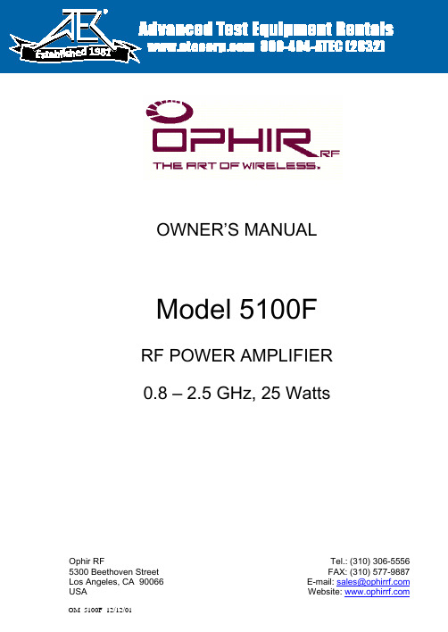
OWNER’S MANUALModel 5100F RF POWER AMPLIFIER 0.8 – 2.5 GHz, 25 WattsOphir RF5300 Beethoven Street Los Angeles, CA 90066 USATel.: (310) 306-5556FAX: (310) 577-9887 E-mail: ***************** Website: OM_5100F 12/12/011981___________________________________________________ CertificationOphir RF certifies that this product met its published specifications at the time of shipment from the factory._____________________________________________________________________ WarrantyThis Ophir RF product is warranted against defects in material and workmanship for a period of two (2) years from date of receipt. During the warranty period, Ophir RF, will,at its option, either repair or replace products that prove to be defective. For warranty service or repair, this product must be returned to a service facility designated by Ophir RF.Limitation of WarrantyThe foregoing warranty shall not apply to defects resulting from improper orinadequate maintenance by Buyer, Buyer-supplied software or interfacing,unauthorized modification or misuse, operation outside of the environmentalspecifications for the product, or improper site preparation or maintenance.NO OTHER WARRANTY IS EXPRESSED OR IMPLIED. OPHIR RF SPECIFICALLY DISCLAIMS THE IMPLIED WARRANTIES OF MERCHANTABILITY AND FITNESS FOR A PARTICULAR PURPOSE.Exclusive RemediesTHE REMEDIES PROVIDED HEREIN ARE BUYER’S SOLE AND EXCLUSIVEREMEDIES. OPHIR RF SHALL NOT BE LIABLE FOR ANY DIRECT,INDIRECT, SPECIAL, INCIDENTAL, OR CONSEQUENTIAL DAMAGES, WHETHER BASED ON CONTRACT, TORT, OR ANY OTHER LEGAL THEORY._____________________________________________________________________ AssistanceFor any assistance, contact your Ophir RF Sales and Service Office.OM_5100F 12/12/01 Page 1 of 14_____________________________________________________________________ Safety InformationThe following safety notes and symbol are used in this manual and on the equipment. Familiarize yourself with each and its meaning before operating this equipment.Caution Caution denotes a hazard. It calls attention to a procedure that, if not correctly performed or adhered to, would result in damage to, ordestruction of, the equipment. Do not proceed beyond a caution noteuntil the indicated conditions are fully understood and met._____________________________________________________________________ Warning Warning denotes a hazard. It calls attention to a procedure which, if not correctly performed or adhered to, could result in injury or lossof life. Do not proceed beyond a warning note until the indicatedconditions are fully understood and met._____________________________________________________________________The instruction documentation symbol. The product is marked with thissymbol when it is necessary for the user to refer to the instructions in thedocumentation._____________________________________________________________________ General Safety ConsiderationsWarning This is a safety Class I product provided with a protective earthing ground incorporated in the AC power cord. The AC power cordshall only be inserted in a socket outlet provided with a protectiveearth contact. Any interruption of the protective conductor, insideor outside of the equipment, is likely to make the equipmentdangerous. Intentional interruption is prohibited._____________________________________________________________________ Warning No operator serviceable parts inside. Refer servicing to qualified personnel. To prevent electrical shock, do not remove covers._____________________________________________________________________ Warning If this equipment is used in a manner not specified by Ophir RF, the protection provided by the equipment may be impaired._____________________________________________________________________ Caution Before switching on this equipment, make sure that the line voltage is correct and that an External Load has been applied. (Refer to 2.2.3)OM_5100F 12/12/01 Page 2 of 14ContentsSection PageInformation 5I GeneralDeclaration of Conformity 5Scope 5Description 5Equipment Specifications 6II Installation 7Incoming Inspection 7Preparation for Use 7Power Requirements 7Earthing 7Load Requirements 7Connections 7CableIII Operation 8Introduction 8AgainstUnspecified Use 8StatementControls, Indicators, and Connectors 8Basic Operating Procedures 8Before Turn On 8Turn On 9Operation 9Turn Off 9IV Maintenance 1010IntroductionTest 10PerformanceProcedures 10AdjustmentProcedures 10TroubleshootingImproper Power Distribution 10Low or No RF Output Power 10Cleaning 10Service 11V CustomerServicing 11Return11(RMA)MaterialAuthorizationShipment11forRepackaging12FormRequestRMAOM_5100F 12/12/01 Page 3 of 14Figuresdiagram 131 BlockFigureFigure 2 System View 14Tables6TableSpecifications1 EquipmentOM_5100F 12/12/01 Page 4 of 14SECTION IGeneral Information1.1 Declaration Of ConformityDECLARATION OF CE CONFORMITYOphir RF Inc., 5300 Beethoven Street, Los Angeles, CA 90066, declares under sole responsibility that the RF Power Amplifier, Model 5100F, to which this declaration relates, meets essential health and safety requirements and is in conformity with ISO 3864. The CE marking has been applied according to the relevant Safety and CE Directives listed below using the relevant section of the following EC standards and other normative documents:EU EMC DIRECTIVE 89/366/EEC - Essential health and safety requirements relating to electromagnetic compatibilityENEN55022 Class BEN50082-1 EC generic immunity requirements, Category A & BIEC801-2, IEC801-3, IEC801-4EC Low Voltage Directive 72/23/EEC Essential health and safety requirements relating to electrical equipment designed for use within certain violate limits.EN61010-1 Safety requirements of Test Measurement and LaboratoryEquipment.1.2 ScopeThis owner’s manual contains operating instructions for a model 5100F amplifier.1.3 DescriptionThe power amplifier operates in the RF frequency. The input to the power amplifier is rated at 0 dBm nominal CW signal between the 0.8 – 2.5 GHz frequency range. The output of the power amplifier is specified at 25 Watts CW RF signal. Detailed specifications for the power amplifier are given in table 1-1. OM_5100F 12/12/01 Page 5 of 14Equipment SpecificationsTable 1-1. Specifications @ 25º COperation:A/ABofClass2.5GHz–Range:Frequency0.8Output Power @ Saturation: 25 Watts CW TypicalOutput Power @ 1 dB Compression: 20 Watts CW minimumdB+45minimumGain:SmallSignalSmall Signal Gain Flatness: ± 2.0 dB maximumnominalohmsInput/OutputImpedance:50Input VSWR: 2:1 maximumdBmInput +10RFMax.Operating Temperature Range: 0º C to 50º COperating Humidity Range: 95%, Non-condensingTemp. Protection: Shut down @ 80º C minimumAirForcedCoolingsystem:InternalAC Input: 100 - 240 VAC, 50/60 Hz, 1¯Wattsmaximum200ACPower:InputDimensions: 19" W x 3.5" H x 18" DmaximumPoundsWeight: 30Option(s) included:-Type-N Connectors on Front Panel.*NOTE – Specifications subject to change without noticeOM_5100F 12/12/01 Page 6 of 14SECTION IIInstallationInspection2.1 IncomingWARNING!Do not apply power until you have read Sections II and III and you have performed all specified procedures. If you fail to observe this warning, damage to the equipment and/or bodily injury may result.The power amplifier has been mechanically and electrically inspected prior to shipment. If the equipment has been damaged or if electrical performance is not within specification, notify the carrier and OPHIR RF immediately.2.2 Preparation For Use2.2.1 Power RequirementsThe power amplifier requires a power source of 100 – 240 VAC, 50/60Hz capable of delivering 200 Watts. Turn off the front panel ‘ON/OFF’switch before connecting the AC power source.2.2.2 EarthingEarthing is achieved simultaneously with connection of the AC powercords to a properly grounded power source.2.2.3 Load RequirementsThe power amplifier requires a load, antenna, or dummy load with a 50-Ohm nominal impedance.CAUTION!Make this external load connection before applying any power to theequipment.2.2.4 Cable ConnectionsThe AC power cable connection is made at the rear of the poweramplifier via the receptacle connector. RF connections for Input andOutput are made at the front via Type-N connectors. (Refer to Figure 2) OM_5100F 12/12/01 Page 7 of 14SECTION IIIOperation3.1 IntroductionThis section describes the operating controls and procedures of the power amplifier.3.2 Statement Against Unspecified UseThis amplifier must be used as specified by the manufacturer. Use of this equipment in any way not specified by the manufacturer may result in bodily injury and/or damage to the equipment.3.3 Controls, Indicators, and ConnectorsWhen set to ‘ON’, the ON/OFF switch will light indicating that AC power is present. The RF INPUT and OUTPUT connections are located on the front of the power amplifier. Refer to figure 2 and the following discussion for the location and functional description of all controls, indicators, and connectors.3.4 Basic Operating ProceduresNOTE!The operation of the power amplifier is passive; that is, after an External Load and Input power have been applied, no procedures other than turn off are required.3.5 Before Turn OnCAUTION!Do not obstruct the airflow at the front and rear of the power amplifier. If you do not verify that this equipment has an unobstructed airflow, you may cause this equipment to overheat or otherwise impair its operation.Perform the following preliminary procedures before energizing the equipment:a. Check that the ON/OFF switch is set to the ‘OFF’ position.b. At the rear of the RF power amplifier, verify that the AC cord is properlyinserted into the receptacle connector.c. Verify that 50 ohm loads are connected to the RF Input and Output ports.3.6. Turn OnPerform the following procedures to energize the equipment:a. Set the ON/OFF switch to the ‘ON’ position. Verify that the green switchlamp is lit.b. Apply RF power.OM_5100F 12/12/01 Page 8 of 14CAUTION!To maintain specified performance and retain certain operating characteristics, RF input power should not exceed +10 dBm.3.7. Operation3.7.1 ON/OFF SwitchIn the ‘ON’ position, AC power is supplied to the power amplifier.3.7.2 ON/OFF Switch LampLights to indicate the distribution of AC power throughout the poweramplifier.3.7.3 TEMP. FAULT IndicatorLights at an internal temperature exceeding 80º C with the amplifierturning off DC bias voltage to the main amplifiers’ modules. DC biasvoltage will automatically return at temperatures below 75º C.Off.3.8 TurnWARNING!In the event of ANY power failure, whenever possible and practical, it is advisable to reset the ON/OFF switch on the front panel to the “OFF”position before y ou reconnect AC power to the power amplifier. This is to prevent any possible electrical damage to the amplifier, due to the initial power surge, once power is restored.Turn off the RF power amplifier by first lowering or removing the RF Input drive level and then placing the ON/OFF switch in the ‘OFF’ position.OM_5100F 12/12/01 Page 9 of 14Maintenance4.1 IntroductionThis section describes the performance tests, adjustments and troubleshooting procedures for the power amplifier.4.2 Performance TestThe performance test is identical to the operating procedure described in Section III.4.3 Adjustment ProcedureThere are no operator adjustments applicable for the power amplifier.4.4 Troubleshooting ProcedureNOTE!Troubleshooting beyond the level described in this procedure must be performed at an authorized service facility or the warranty may be voided.The following troubleshooting procedure is to be used as a guide to help ascertain whether the equipment is malfunctioning.4.4.1 Improper Power DistributionWhenever there appears to be improper power distributed throughout theamplifier, perform the following steps:a. Verify the ‘ON/OFF’ switch lamp is illuminated on the front panel.b. Verify that the internal fans are operating.c. If neither step A or B above appear to be working, verify the presenceof AC power at the source and also at rear panel connection.4.4.2 Low or No RF Output PowerWhenever the RF output power of the amplifier and/or the current drawnfrom the power supply is low, or the operating temperature has exceeded80°C, the system may have triggered the thermal protection function.Perform the following procedure:a. Verify that the drive level is correct.b. Check that the ‘TEMP. FAULT’ indicator is not illuminated.If the above conditions are verified and there is still low or no RF outputpower, then contact your nearest authorized Ophir RF Service Center. 4.5. CLEANINGUse a rag with isopropyl alcohol to clean exterior surfaces. Use a vacuum to remove dust from the screens on the front and rear of the equipment.Customer Service5.1 ServicingAll servicing and repair must be done by an authorized repair and servicing facility.5.2 Return Material Authorization (RMA)In the unlikely event you experience equipment difficulties that can not be resolved without opening up the equipment, you will need to obtain authorization and an RMA number prior to returning the equipment.NOTE!It is Ophir RF’s policy not to accept any returned equipment without an authorized RMA number!5.3 Repackaging for Shipment.WARNING!It is always recommended that two people carry this system due to its weight.Use the original shipping container and packing materials if possible. If these have been discarded or are not in good condition for reuse, use a heavy-duty carton capable of providing adequate protection. Whenever the amplifier is being returned to the manufacturer, attach an identifying tag, indicating the RMA number, on the outside of the container.Wrap the equipment in heavy paper or plastic, and use enough shock-absorbing material (3 to 4-inch layers) around all sides to provide a firm cushion and to prevent movement within the container. Protect the front and rear panels with cardboard or foam blocks. Seal the shipping container securely and mark the container "FRAGILE".To receive your RMA number, contact our customer service department.Customer ServicePhone: 310-306-5556Fax: 310-577-9887Email: ***************************You will be required to complete a simple questionnaire prior to receiving your RMA number. Once you have your RMA number, you are authorized to return your equipment.To help you expedite this process, we have included a copy of the form you will be required to complete prior to receiving your RMA number.5300 Beethoven Street, Los Angeles, CA 90066Tel: (310) 306-5556 • FAX (310) 577-9887 •e-mail:***************************RMA REQUEST FORMRMA NUMBER:NAME:CUSTOMERRECEIVEDROM RESS:F ADD(STREET ADDRESS – INCLUDING SUITE OR M/S NUMBER)(CITY – STATE – ZIP OR COUNTRY CODE) (COUNTRY)RETURN TOADDRESS:(STREET ADDRESS – INCLUDING SUITE OR M/S NUMBER)(CITY – STATE – ZIP OR COUNTRY CODE) (COUNTRY)CONTACT PERSON:(FIRST AND LAST NAME) (TITLE/RANK)(TELEPHONE) (FAX)(E-MAIL)MODEL NUMBER SERIAL NUMBERREASON FOR RMA:PLEASE FAX THIS FORM TO OPHIR RF, INC.AT (310) 577-9887 ATTN: CUSTOMER SERVICETHERE IS A $500 MINIMUM EVALUATION CHARGE FOR ALL NON-WARRANTY REPAIRS. PURCHASE ORDER TO BE PRESENTED PRIOR TO COMMENCEMENT OF REPAIRS. FOLLOWING EVALUATION, THE COST OF REPAIRS WILL BE SUBMITTED FOR YOUR APPROVAL AND PURCHASE ORDER AMENDMENT.DO NOT SHIP AMPLIFIERS C.O.D. – OPHIR RF WILL NOT ACCEPT ANY C.O.D. SHIPMENTS. PLEASE CALL US WITH ANY SHIPPING QUESTIONS.。
实验一 射频前端发射和接收器
(8)三阶互调截止点( THIRD-ORDER INTERCEPT POINT,IP3)
其中IP3——混频器的输入三阶互调截止点。
PIN——混频器输入端的输入信号的功率。
Δ——混频器输出端中,设计输出信号与内调制(INTER-MODULATION,IM)信号的功率差(dB)
8.载波滤波器(LO BPF)
9.发射天线(Antenna)
其中放大器的基本原理与设计方法可参考主题六,而滤波器的基本原理与设计方法已可参考主题五的说明。至于振荡器的部分,可于主题八与与主题九获得一些参考。天线部分则可由主题十得到概念。 所以,在此单元中将就上变频器部分的基本原理做一说明。并介绍发射器的几个重要设计参数。
除非有特别注明,一般的变频损耗皆按上式定义,即单边带变频耗损( SINGLE-SIDEBAND(SSB) CONVERSION LOSS ), 即只考虑射频输出信号频率为fLO+fIF或fLO-fIF。若是定义为双边带变频损耗(DOUBLE-SIDEBAND(DSB) CONVERSION LOSS), 则比单边带转频损耗低3dB。
6
直流电源连接线
1条
DC-1
7
ADS软件
1套
微波软件
四、理论分析:
基本结构与设计参数说明:
在无线通讯中,射频发射器担任着重要的角色。无论是话音还是数据信号要利用电磁波传送到远端,必须使用射频前端发射器。如图1-1(a)所示,它大抵可分成九个部分。
1.中频放大器(IF Amplifier)
2.中频滤波器(IF Bnadpass Filter)
其中,IP2——混频器的输入二阶互调截止点。(dBm)
射频功率放大器芯片

射频功率放大器芯片射频功率放大器(RF power amplifier)是一种用于放大射频信号的电子设备,广泛应用于无线通信系统、雷达系统、卫星通信系统、广播电视系统等领域。
它的主要作用是将输入的低功率射频信号放大到足够大的功率,以便能够远距离传输或驱动其他设备。
射频功率放大器芯片是射频功率放大器的核心元件,其主要功能是将输入的低功率射频信号放大到更高的功率。
射频功率放大器芯片通常由半导体材料制成,最常见的是使用金属氧化物半导体场效应管(MOSFET)或互补金属氧化物半导体(CMOS)技术。
射频功率放大器芯片通常具有以下特点:1. 宽带特性:射频功率放大器芯片能够在很宽的频段内进行工作,从几十兆赫兹到几千兆赫兹不等,能够适应不同的工作频段和应用需求。
2. 高功率增益:射频功率放大器芯片能够将输入信号的功率放大到较高的水平,通常能够提供几瓦到几十瓦的输出功率。
高功率增益可以确保信号的传输距离更远,同时也能够驱动各种外部设备。
3. 高效能率:射频功率放大器芯片通常能够实现较高的功率放大效率,能够将输入的电能有效地转化为输出的射频功率,减少能量的浪费,并减少热量的产生。
4. 低噪声:射频功率放大器芯片通常具有较低的噪声指标,能够保证输出信号的清晰度和稳定性,提高接收信号的质量。
5. 兼容性:射频功率放大器芯片通常具有较高的兼容性,能够适应不同的工作环境和系统要求,同时还能够与其他射频设备和控制电路进行连接和集成。
射频功率放大器芯片在无线通信系统中起着至关重要的作用。
它能够增强信号的强度和传输距离,保证信号的可靠传输,提高通信质量。
同时,射频功率放大器芯片还能够用于雷达系统中的信号增强、卫星通信系统中的信号放大、广播电视系统中的信号驱动等各种应用领域。
总之,射频功率放大器芯片是无线通信系统中至关重要的核心元件,它能够将输入的射频信号放大到足够大的功率,实现信号的长距离传输和驱动其他设备。
随着无线通信技术的发展和应用需求的增加,射频功率放大器芯片将会继续发展和创新,为无线通信领域的进一步发展做出重要贡献。
射频电源的功率调节技术研究与优化
射频电源的功率调节技术研究与优化射频电源的功率调节技术研究与优化随着科技的不断发展,射频(Radio Frequency,RF)电源在无线通信、雷达系统和卫星通信等领域的应用越来越广泛。
在射频电源的设计和优化过程中,功率调节是一个重要的环节。
功率调节技术的研究与优化对于提高射频电源的性能和效率至关重要。
功率调节是指调节射频电源输出功率的过程。
在射频系统中,功率调节主要实现在射频功率放大器(RF Power Amplifier,PA)中。
射频功率放大器通常由多个功率调节级(Power Control Stage)组成。
每个功率调节级都具有一定的输出功率范围和调节能力。
功率调节技术的目标是在尽可能大的功率调节范围内,保证输出功率的稳定性和精确性,并最大限度地提高射频功率放大器的效率。
射频电源的功率调节技术主要包括直接功率调节技术和间接功率调节技术两种方法。
直接功率调节技术是直接调节射频功率放大器的输入信号强度来实现功率调节。
这种方法通常具有较高的调节带宽和快速响应时间,但在某些功率范围内可能存在效率低和线性度差等问题。
间接功率调节技术是通过增加或减小射频功率放大器的负载来实现功率调节。
这种方法一般具有较高的效率和较好的线性度,但在调节速度和带宽方面可能略逊于直接功率调节技术。
在功率调节技术的研究与优化过程中,需要考虑多个因素。
首先是功率调节的精确性和稳定性。
射频电源在工作过程中可能会受到温度、电源电压等因素的影响,因此需要采用一定的补偿措施来保证输出功率的精确性和稳定性。
其次是功率调节的效率问题。
射频功率放大器的效率直接影响到射频电源的工作效率和散热问题,因此需要在功率调节技术中考虑如何提高功率放大器的效率。
最后是功率调节的动态特性。
射频电源在不同的工作状态下,功率调节的要求也不同,因此需要在设计中考虑如何实现快速响应和稳定性的平衡。
为了提高射频电源的功率调节技术和优化,可以采用以下一些策略。
首先是采用先进的功率调节芯片和控制算法。
射频功放功率 计算

射频功放功率计算射频功放(RF Power Amplifier)是一种将射频信号的功率放大的电子器件。
在无线通信领域中,射频功放被广泛应用于无线电通信设备、卫星通信、雷达系统和无线电电视等领域。
射频功放的功率计算是评估射频功放性能和设计电路的重要指标之一。
射频功放的功率计算主要涉及到输入功率和输出功率的关系。
输入功率是指射频功放接收到的信号的功率,输出功率则是指射频功放输出的信号的功率。
根据能量守恒定律,输入功率和输出功率之间存在一定的关系。
在射频功放的设计中,一个重要的参数是功率增益(Power Gain),它是输出功率与输入功率之间的比值。
功率增益可以用来评估射频功放的放大效果,也可以用来计算输出功率。
通常情况下,功率增益是以分贝(dB)为单位来表示的。
功率增益的计算公式如下:功率增益(dB)= 10 * log10(输出功率/输入功率)根据功率增益的计算公式,我们可以得到输出功率的表达式:输出功率 = 输入功率 * 10^(功率增益/10)在实际应用中,射频功放的功率计算还需要考虑一些其他因素。
例如,射频功放的效率(Efficiency)是指输出功率与输入功率之间的比值。
功率计算中的效率可以通过以下公式来表示:效率(%)= 输出功率 / 输入功率 * 100%射频功放的线性度(Linearity)也是功率计算中需要考虑的因素之一。
线性度是指射频功放在放大过程中是否能够保持输入信号的波形不变。
线性度的好坏直接影响到射频功放的输出信号质量。
除了功率增益、效率和线性度,射频功放的功率计算还需要考虑一些其他因素,如工作频率、负载匹配和电源电压等。
这些因素都会对射频功放的功率特性产生影响,需要在设计和计算中进行综合考虑。
射频功放的功率计算是评估射频功放性能和设计电路的重要指标之一。
通过合理计算和综合考虑功率增益、效率、线性度等因素,可以有效地评估和设计射频功放的性能。
在实际应用中,我们需要根据具体需求和设计要求,选择合适的射频功放,并进行相应的功率计算和优化,以满足无线通信系统的要求。
RF PA介绍

RF PA介绍LOREM IPSUM DOLOR LOREMCONTENTS 半导体功率器件放大器类型介绍RF PA调试QA RF PA应用RF PA特性参数PA:独立于主芯片的射频器件射频功率放大器(Power Amplifier, 简称 PA)是化合物半导体应用的主要器件,也是无线通信设备射频前端核心的组成部分。
射频前端(RF Front End)是用以实现射频信号发射与接收功能的芯片组,与基带芯片协同工作,共同实现无线通讯功能。
射频前端包括功率放大器(Power Amplifier)、开关(Switch)、滤波器(Filter)、双工器(Duplexer)、低噪声放大器(Low Noise Amplifier)等功能构件,其中核心器件是决定发射信号能力的射频功率放大器芯片。
PA 芯片的性能直接决定了手机等无线终端的通讯距离、信号质量和待机时间,是整个通讯系统芯片组中除基带主芯片之外最重要的组成部分。
根据晶体管的静态工作点的位置不同可分以下几类。
(1) A 类放大电路u CEi CQ Ai C1I CQ ωt2θ=2π 02ππ集电极电流波形静态工作点位置特点a.静态功耗大b.能量转换效率低c.高线性度功率放大器分类CQCEQ C I U P =u CEi CQ Aωti C2π 2 π2θ = π3 π静态工作点位置集电极电流波形特点a. 静态功耗CQ CEQ C ≈=I U P b. 能量转换效率高c. 输出失真大(2) B 类放大电路B类放大电路图示分析-U CC+U CCR 1R 2R Lu oVD 1VD 2u iV 1V 2u i wt+U CCu i+-V 1R Lu oV 2R Lu ou i-U CCu owt 0u owt0u owt 0改善B类放大器交越失真u CEi CQ Ai C3π2π3πI CQπ <2 < 2π静态工作点位置集电极电流波形特点a. 静态功耗较小b. 能量转换效率较高c. 输出失真比甲类大(3) AB 类放大电路功率放大器特性总结Linearity class MaximumefficiencyA50%GoodB78.5%ModerateAB50-78.5%betterC100%poor半导体功率器件晶体管工艺Class ProcessHigh power PA HBTLow/Mid power PA SiGeLNA+Switch HEMT/pHEMT/SOI/SiGeHigh power FEM HBT+HEMT/pHEMT,BiHEMT FEM(Low/Mid power)HBT/SiGeRF PA应用802.11 wifi802.15 Bluetooth/Zigbee GSM/CDMA/LTE-A通信类电子射频前端ISM Band Application射频前端架构图PA内部架构图PA与LNA区别●LNA:工作在小信号状态,提供放大的信号电流和电压,功率通常很小,NF低;●PA:工作在大信号状态,提供较大的功率输出,其晶体管有足够的电流驱动能力和较高的击穿电压;●PA:输出有很大的动态范围,其输出阻抗随电压和电流而改变,是非线性阻抗,因此阻抗匹配是难点;●LNA:电压增益;●PA:电压增益+功率增益。
RF Power Amplifier Design
RF Power Amplifier DesignMarkus Mayer & Holger ArthaberDepartment of Electrical Measurements and Circuit DesignVienna University of TechnologyJune 11, 2001Contents¤Basic Amplifier Conceptsl Class A, B, C, F,hHCAl Linearity Aspectsl Amplifier Example¤Enhanced Amplifier Conceptsl Feedback, Feedforward, ...l Predistortionl LINC, Doherty, EER, ...3Efficiency Definitions¤Drain Efficiency:¤Power Added Efficiency: DCOUT D P P =η−⋅=−=G P P P D DC IN OUT PA 11ηηIdeal FET Input and Output CharacteristicsDDKDD V V V −=κ0V GSI DS I m2V P V P V DSmaxV DDV K V DS0V =V GS PV =0GS Ohmic SaturationBreakdowng m5Maximum Output Power MatchmKDS OPT I V V R −=max 0V GSI DS I m2V P V P V DSmaxV DDV K V DS0V =V GS P V =0GS Ohmic SaturationBreakdowng mClass AV GS I DS I m2V P V P V DSmaxV DD V K V DS 0V GSV DS2p pQI DS I m02pp Q7Class A –CircuitV DDR LD GS48%dB) 14 (e.g. 50%PA ⋅==⋅=κηκηA D G G Class BV GS I DS I m2V P V P V DSmaxV DD V K V DS 0V GSV DS2p pQI DS I m02pp Q9Class CV GS I DS I m2V P V P V DSmaxV DD V K V DS 0V GSV DS2p pQI DS I m02pp QClass B and C –Circuit%65dB) (8 6dB -%78⋅==⋅=κηκηA D G G %01%100→→→ηηG D V DDR LD GSf 0Class BClass C11Influence of Conduction AngleClass F (HCA ... harmonic controlled amplifier )V GS I DS I m2V P V P V DSmaxV DD V K V DS 0V GSV DS2p pQI DS I m02pp Q13hHCA(half sinusoidally driven HCA)V GS I DS I m2V P V P V DSmaxV DD V K V DS 0V GSV DS2p pQI DS I m02pp QClass F and hHCA –CircuitV DDR LV DSI DZ e (n)0, n=even inf, n=evenZ o (n)0, n=1inf, n=odd%87dB) (9 5dB -0%10⋅==⋅=κηκηA D G G Class FhHCA%96dB) (15 1dB 0%10⋅=+=⋅=κηκηA D G G15hHCA –Third Harmonic PeakingV GS I DS I m2V P V P V DSmaxV DD V K V DS 0V GSV DS2p pQI DS I m02pp QThird Harmonic Peaking –CircuitV DDR LD GSf 03f 0%87dB) (14.6 0.6dB 91%PA ⋅=+=⋅=κηκηA D G G17 Linearity AspectsLinearity Aspects¤Class A ¤Class B ¤Class AB ¤Class CLinearity Aspects¤Ideal strongly nonlinear model¤Strong-weak nonlinear model19Amplifier Design –An Example¤Balanced Amplifier ConfigurationPort 1Z=50 Ohm Port 2Z=50 Ohm21Amplifier Design –Simulation¤Gate & Drain Waveforms50010001300Time (ps)Drain waveforms-5510152025-1000010002000300040005000050010001300Time (ps)Gate waveforms-3-2-101-1000-50005001000Amplifier Design –Simulation¤Dynamic Load Line & Power Sweep3691215Voltage (V)Dynamic load line-200020004000600080000510152024Power (dBm)Power Sweep 1 Tone010203040102030405060708023Amplifier Design –Measurements¤Single Tone & Two Tone00000000 0000000000 Amplifier Nonlinearity¤Gain and Phase depends on Input Signal ¤3rd Order Gain-Nonlinearities:Amplifier Nonlinearity¤Higher Output Level (close to Saturation) results in more Distortion/Nonlinearity25Nonlinearity leads to?¤Generation of Harmonics¤Intermodulation Distortion / Spectral Regrowth¤SNR (NPR) Degradation¤Constellation Deformation27Intermodulation and HarmonicsSpectral Regrowth¤Energy in adjacent Channels¤ACPR (Adjacent Channel Leakage Power Ratio) increases-15-10-5051015-60-50-40-30-20-10010r e l a t i v e p o w e r / d Brelative frequency / MHzACPR 1>60dB ACPR 2>60dB ACPR 1=16dB ACPR 2=43dB29Reduced NPR (Noise Power Ratio)¤Input Signal¤Degradation of Inband SNR ¤…Noisy“ Constellation¤Output Signal of Nonlinear AmplifierConstellation Deformation¤Input Signal¤Output Signal of Nonlinear Amplifier(with Gain-and Phase-Distortion)31Modeling of Nonlinearities¤with Memory-Effectsl Volterra Series (=…Taylor Series with Memory“)¤without Memory-Effectsl Saleh Model l Taylor Seriesl Blum and Jeruchim Modell AM/AM-and AM/PM-conversion2221)(1)(r r r g r r r f a a ΘΘ+=+=βαβαb e t t e r p e r f o r m a n c eAM/AM-and AM/PM-Conversion¤GaAs-PAAM/AM-and AM/PM-Conversion¤LDMOS-PA33How to preserve Linearity?¤Backed-Off Operation of PAl Simplest Way to achieve Linearity¤Linearity improving Conceptsl Predistortionl Feedforwardl...How to preserve Efficiency?¤Efficiency improving Conceptsl Dohertyl Envelope Elimination and Restorationl...¤Linearity improving Conceptsl Higher Linearity at constant EfficiencyàHigher Efficiency at constant Linearity35 Direct (RF) Feedback¤Classical Method¤Decrease of Gain àLow Efficiency¤Feedback needs more Bandwidth than Signal¤Stability Problems at high BandwidthsDistortion Feedback¤Feedback of outband Products only¤Higher Gain than RF feedback¤Stability Problems due to Reverse Loop37 Feedforward¤Overcomes Stability Problem by forward-only Loops¤Critical to Gain/Phase-Imbalances0.5dB Gain Error à-31dB Cancellation2.5°Phase Error à-27dB Cancellation¤Well suited for narrowband application39-30-20-100102030-60-50-40-30-20-10010r e l a t i v e p o w e r / d Brelative frequency / MHzoriginal signal predistorted signalCartesian Feedback¤AM/AM-andAM/PM-correction¤High Feedback-Bandwidth ¤Stability ProblemsIQI QI Qmodulator demodulatorOPAsmain amp.local oscillatorRF-outputb a s e b a n d i n p u tUMTS example :Digital Predistortion¤Digital Implementation of …Cartesian Feedback“¤Additional ADCs, DSP Power,Oversampling needed ¤Loop can be opened àno Stability ProblemsAnalog Predistortion¤Predistorter has inverse Function of Amplifier¤Leads to infinite Bandwidth (!)¤Hard to realize (accuracy)41Analog Predistortion¤Possible Realizations:43LINC (Linear Amplification by Nonlinear Components)¤AM/AM-andAM/PM-correction¤Digital separation required (accuracy!)¤High Bandwidth,oversampling necessary ¤Stability guaranteedsignal separations(t)s (t)1KKs (t)2K(s (t)+1s (t))=Ks(t)2Ks (t)1Ks (t)2-30-20-100102030-60-50-40-30-20-10010r e l a t i v e p o w e r / d Brelative frequency / MHzACPR 1>60dB ACPR 2>60dB ACPR 1=18dB ACPR 2=29dBs(t) s 1(t)UMTS example :Doherty Amplifier¤Auxiliary amplifier supports main amplifier during saturation ¤PAE can be kept high over a 6dB range45Doherty Amplifier¤Gain vs. Input Power¤No improvement of AM/AM-and AM/PM-distortion¤Behavior of auxiliary amplifier very hard (impossible) to realize ¤Stability guaranteed¤Efficiency vs. Input Powermain amp. (A1)aux. amp. (A2)P P d oh e r t y c o nf ig u r a t i on(A 1+A 2)EER (Envelope Elimination and Restoration)¤Separating phase and magnitude information ¤Elimination of AM/AM-distortion¤Application of high-efficient amplifiers (independent of amplitude distortion)¤Stability guaranteedsignal separationamplitude informationphase informationRF inputRF outputhigh efficiency power amplifier47EER (Envelope Elimination and Restoration)¤Analog realizationl Limiter hard to build l Accuracy problems l Feedback necessary¤Digital realizationl Oversampling + high D/A-conversion rates required l High power consumption of DSP and D/A-converters l Possible feedback eliminationl Compensation of AM/PM-distortion possibleDADA DAamplitude informationphase informationmodulator RF outputhigh efficiency power amplifierdigital signal processorlocal oscillatorsupply voltage amplifierI QI Qd i g i t a l b a se b a n d i n p u tpeak detectorsupply voltage amplifier limiterhigh efficiency power amplifierRF outputpeak detectorRF inputEER (Envelope Elimination and Restoration)¤Bandwidth of Magnitude-and phase-signal have higher than transmit signal¤Five times (!)oversampling necessary to achieve standard requirements-30-20-100102030-60-50-40-30-20-10010r e l a t i v e p o w e r / d Brelative frequency / MHzMagnitude Phase-30-20-100102030-60-50-40-30-20-10010r e l a t i v e p o w e r / d B relative frequency / MHzACPR 1>60dB ACPR 2>60dB ACPR 1=33dB ACPR 2=40dB ACPR 1=51dB ACPR 2=36dB ACPR 1=53dB ACPR 2=49dBfull bandwidth 3⋅B 0 bandwidth 5⋅B 0 bandwidth 7⋅B 0 bandwidthUMTS example :UMTS example :49Adaptive Bias¤Varying/Switching of Bias-Voltage depending on Input Power Level¤Selection of Operating Point with high PAE ¤Applicably for nearly each type of AmplifierRF input peak detectorbias controlRF outputhigh efficiency power amplifier3233343536373839402030405060708090output power / dBmp o w e r a d d e d e f f i c i e n c y / %V D =3.5V V D =4.5V V D =6.5VAdaptive Bias¤Single tone PAE for switched V DD with V G kept constant¤Simply to implement Concept ¤Stability guaranteed ¤Possible problems:l DC-DC converter with high efficiency necessaryl Possible Linearity Change (can increase and decrease)especially for HCAs51Summary¤Digital Realization required to achieve Accuracy ¤Problem of Stability for high Bandwidth Application ¤Higher Bandwidths (Oversampling) necessary,depending on Order of IMD cancellation ¤Predistortion gives best Results while keepingEfficiency high (valid for high Output Levels > 40dBm)Figure References¤F. Zavosh et al,“Digital Predistortion Techniques for RF Power Amplifiers with CDMA Applications”,Microwave Journal, Oct. 1999¤Peter B. Kenington,“High-Linearity RF Amplifier Design”,Artech House, 2000¤Steve C. Cripps,“RF Power Amplifiers for Wireless Communications”,Artech House, 1999Contact InformationDI Markus Mayer(+43-1-58801-35425-markus.mayer@tuwien.ac.atDI Holger Arthaber(+43-1-58801-35420-holger.arthaber@tuwien.ac.at53。
射频功放的偏置电压

射频功放的偏置电压
射频功放(RF Power Amplifier)是一种用于增强射频信号的
设备,常用于无线通信系统中。
而射频功放的偏置电压则是其工作
中至关重要的一个参数。
偏置电压是指在射频功放的晶体管或集成
电路中施加的直流电压,用来控制晶体管的工作状态。
偏置电压的大小直接影响着射频功放的工作性能。
如果偏置电
压设置不当,可能会导致功放工作不稳定、功率输出不足或者过载,甚至损坏设备。
因此,合理设置偏置电压是射频功放设计中的重要
环节。
一般来说,合适的偏置电压能够保证射频功放在工作时具有良
好的线性和高效率。
在设计中,工程师需要根据具体的射频功放器
件和工作频率来选择合适的偏置电压值,并通过实验和测试来优化
偏置电压的设置。
此外,随着射频功放技术的不断发展,一些先进的功放器件可
能会采用自动偏置控制技术,能够根据工作条件动态调整偏置电压,以实现更高的性能和更低的功耗。
总之,射频功放的偏置电压是射频系统设计中不可忽视的重要参数,合理设置偏置电压将有助于提高功放的性能和可靠性,从而更好地满足无线通信系统的需求。
预失真技术在射频功率放大器设计中的应用

Then the main points of RF power amplifier design are presented mad the design
amplifier process of a 1 6W RF power
is performed including simulation with ADS
The paper begins with the nonlinear effects of RF power amplifier,then
introduces common linearization techniques such as feedback、feedforward、 predistortion and the advantages and disadvantages of each technique are discussed.
and PCB drawing with protel.Then RF predistortion linearization is analyzed,where
the anti—parallel diodes predistortion generator is used.For a two-tone signal,three
optimized predistortion 25W power amplifier.And two types of predistortion
linearization which independently control IMD3 and IMD5 are presented,one uses
求。 因此为了适应现代通信系统发展的要求,有必要采用线性化技术来对射频
功率放大器进行改善,以提高系统的性能,减小系统体积,降低系统的需求功 率和系统成本。采用线性化技术可以有效消除系统内的干扰和失真,特别是对 于功率放大器来说,可以在给定失真指标的情况下,工作在更高的功率电平上, 可以提高功率放大器的最大输出功率、效率,并改善功率放大器的线性度,增 加功率放大器的工作带宽,使其符合无线通信系统的指标要求。
射频电路设计要点
射频走线应该注意的问题 如前所述,射频走线的长度要尽量短,线宽严格按照计算好的值去设定。在走 线是尤其要注意的是,射频走线中不要有任何带有尖状的折点,在走线的转折 处,最好要用弧线来实现,如下图
其次,在多层板的走线中,有可能重要的射频线要产生不可避免的交叉,这时 我们就要使用我们最不想使用的东西:过孔。这样,会有部分射频信号线走到 底层甚至中间层,但无论是哪一层,射频走线一定会有参考平面,这时一个值 得注意的问题就是不要跨层,或者说不要使地平面不连续。 过孔的放置 过孔的放置真的是一件比较复杂的事情,本文只讨论那种接地的过孔。 首先,射频走线的旁边的地线最好能通过过孔打穿,接到底层或者中间层的地 平面上,这样可以是任何干扰信号或者辐射有最短的到地的通路,但是,过孔 与射频信号线的距离又不能太近,否则会严重影响射频信号质量,在实际的设 计过程中可灵活把握,如下图,我们看到,高亮的信号线两层分布着很多过 孔。
良好的电源去耦技术与严谨的 PCB 布局、Vcc 引线(星型拓扑)相结合,能够为 任何 RF 系统设计奠定稳固的基础。尽管实际设计中还会存在降低系统性能指 标的其它因素,但是,拥有一个“无噪声”的电源是优化系统性能的基本要素.
【3】射频 PCB 设计的 EMC 规范
1 层分布
1.1 双面板,顶层为信号层,底面为地平面。
(2)如果电路中使用了开关电源,开关电源的外围器件布局要符合各功率回流路 径最短的原则。滤波电容要靠近开关电源相关引脚。 使用共模电感,靠近开关 电源模块。
(3)单板上长距离的电源线不能同时接近或穿过级联放大器(增益大于 45dB)的输出和输入端附近。避免电源线成为 RF 信号传输途径,可能引起自 激或降低扇区隔离度。长距离电源线的两端都需要加上高频滤波电容,甚至中 间也加高频滤波电容。
手机的构成和主要概念

中频(IF):主要功能为将RF进来的讯号经过降频处理后供基频(BB)使用。主要元件有锁相环电路(PLL)电压控制震荡器(VCO)温度控制震荡器(TCXO)调变调节变器(MOD/DEMODULATOR)表面声波滤波器(SAW FILTER)等。近年来,中频部分已逐渐与射频组件整合的趋势,部分IF线路与RF整合,另一部分则与BB整合,向直接降频,即零中频(ZERO INTERMEDIATE)发展。
二.基频模块(BASE BAND MODULE)
基频模块:主要功能为处理传送过来的数字讯号,除负责人机接口的控制与通讯协议的管理外,尚包括压缩/解压缩、资料加密/解密、解调变、频道等化等功能。主要组件包含了DSP、MCU及内存,对外则连接LED、键盘等装置。
DSP是芯片整合的最基本的部分,以下简单介绍DSP:
传送器,接收器 发射信号,接收信号
PA 放大功率产生高频讯号
SYNTBESIZER 产生固定频率信号
A/D D/A调变解调器 射频降为中频,模拟讯号转为数字讯号;或是中频转换为射频,数字讯号转为模拟讯
DSP 语音讯号压缩/解压缩,错误更正编/译码,资料加密/解密,解调变,频道等化,资料格式封装
MCU 人机接口控制,通讯协议管理
内存 包括FLASH与SRAM,负责软件与资料的储存工作
功率放大器(PA):主要功能为提供整个手机运作的功率,属于线性IC的一种。PA是整个发射端最耗电的组件,因此除了低噪声的要求之外,影响通话与待机时间的能量转换效率也是重要考量;PA也是射频中最难取得且最昂贵得零组件,材料方面,包括硅(BICMOS).GaAs.硅锗化合物等。
L波段高效率射频功率放大器的设计与仿真
L波段高效率射频功率放大器的设计与仿真作者:杨小川来源:《数字技术与应用》2014年第11期摘要:射频功率放大器是无线通信系统中的重要组成部分,其工作效率直接影响着整个系统的耗能、稳定度和对电源散热装置的要求,提高射频功率放大器的效率,能够节约能源,降低功耗,因此实现射频功率放大器的高效率工作是目前射频功率放大器领域的热点问题之一。
本文选用Freescale晶体管MW6S004N,借助ADS2013软件,采用负载牵引技术和源牵引技术得到最佳负载阻抗和最佳源阻抗,并用Smith圆图进行电路的匹配设计,对射频功率放大器进行了仿真和优化。
仿真结果表明,在频率为1960MHz的L波段,输入功率为21dBm时,射频功率放大器的输出功率大于36dBm,功率附加效率大于50%。
这种高效率射频功率放大器适用于WCDMA基站,对基站中高效率功率放大器的设计有着重要的参考价值。
关键词:射频功率放大器 L波段高效率 ADS2013中图分类号:TN432 文献标识码:A 文章编号:1007-9416(2014)11-0176-06Abstract:RF power amplifier is an important component of wireless communication system,Its efficiency directly affects energy consumption , stability of the whole system and the requirements for power cooling unit.Improve the efficiency of RF power amplifiers can save energy,reduce power consumption, so high efficiency RF power amplifier is the mainstream. In this paper, we select the transistors MW6S004N of Freescale, through ADS2013 software, using load-pull technology and source-pull technique to get optimum load impedance and optimum source impedance, and use the Smith chart to match the circuit design, Finally, simulation and optimization the RF power amplifier. Simulation results show that at the frequency of 1960MHz in the L-band, the input power is 21dBm, the RF amplifier output power greater than 36dBm, the power added efficiency greater than 50% .get a high efficiency RF power amplifier that used for the base station of WCDMA. Therefore, this method has important reference value to design high efficiency power amplifier that used for base station.Key Words:RF power amplifier; L-band; High efficiency;ADS20131 引言射频功率放大器作为发射机最重要的部分之一,它的性能与整个通信系统的性能息息相关,射频功率放大器位于发射机的末端,在整个系统中耗能最多,产热最高,若它的效率过低,不仅很大程度上浪费能量,而且散热问题也将会导致系统的使用寿命缩短[1]。
RF pulse power amplifier
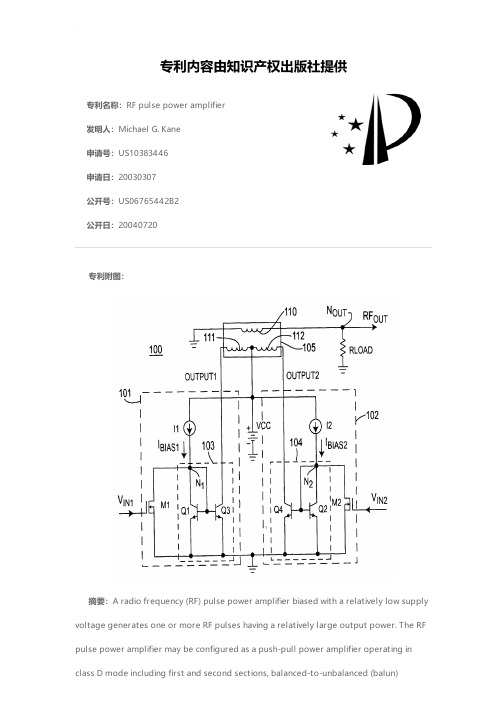
专利名称:RF pulse power amplifier发明人:Michael G. Kane申请号:US10383446申请日:20030307公开号:US06765442B2公开日:20040720专利内容由知识产权出版社提供专利附图:摘要:A radio frequency (RF) pulse power amplifier biased with a relatively low supply voltage generates one or more RF pulses having a relatively large output power. The RF pulse power amplifier may be configured as a push-pull power amplifier operating in class D mode including first and second sections, balanced-to-unbalanced (balun)transformer, and a load resistor coupled across the output winding of the balun transformer. Each section has a current source providing bias current, a MOS transistor, and a pair of bipolar transistors. Each section receives its input digital signal at the MOS transistor, which acts as a current switch for a bias current from a current source. With a relatively small voltage change in response to the input digital signal, the MOS transistor switches the bias current between itself and a transistor pair used to drive the corresponding half (input winding) of the balun transformer.申请人:SARNOFF CORP代理人:William J. Burke, Esq.更多信息请下载全文后查看。
RF pulse power amplifier

专利名称:RF pulse power amplifier发明人:Michael G. Kane申请号:US10383446申请日:20030307公开号:US20030179044A1公开日:20030925专利内容由知识产权出版社提供专利附图:摘要:A radio frequency (RF) pulse power amplifier biased with a relatively low supply voltage generates one or more RF pulses having a relatively large output power. The RF pulse power amplifier may be configured as a push-pull power amplifier operating in class D mode including first and second sections, balanced-to-unbalanced (balun)transformer, and a load resistor coupled across the output winding of the balun transformer. Each section has a current source providing bias current, a MOS transistor, and a pair of bipolar transistors. Each section receives its input digital signal at the MOS transistor, which acts as a current switch for a bias current from a current source. With a relatively small voltage change in response to the input digital signal, the MOS transistor switches the bias current between itself and a transistor pair used to drive the corresponding half (input winding) of the balun transformer.申请人:KANE MICHAEL G.更多信息请下载全文后查看。