Dominant mode in the cuprates electronic vs. phononic scenario
核专业英语词汇

核专业英语词汇d d reaction d d反应d d reactor d d反应器d t fuel cycle d t燃料循环d t reactor d t反应堆daily fuel consumption 燃料日消耗量dalitz pair 达立兹对damage 损伤damage criteria 危害判断准则damp 湿气damp proof 防潮的damped oscillations 阻尼震荡damped vibration 阻尼震荡damped wave 阻尼波damper 减震器damping 衰减的damping factor 衰减系数danger coefficient 危险系数danger dose 危险剂量danger range 危险距离danger signal 危险信号dark current 暗电流dark current pulse 暗电瘤冲data 数据data acquisition and processing system 数据获得和处理系统data base 数据库data communication 数据通信data processing 数据处理data reduction equipment 数据简化设备dating 测定年代daughter 蜕变产物daughter atom 子体原子daughter element 子体元素daughter nucleus 子体核daughter nuclide 子体核素davidite 铈铀钛铁矿dc 直流dc amplifier 直僚大器dc generator 直立电机dc motor 直羚动机dc voltage 直羚压de broglie equation 德布罗意方程de broglie frequency 德布罗意频率de broglie relation 德布罗意方程de broglie wave 德布罗意波de broglie wavelength 德布罗意波长de excitation 去激发de exemption 去免除deactivation 去活化dead ash 死灰尘dead band 不灵敏区dead space 死区dead time 失灵时间dead time correction 死时间校正deaerate 除气deaeration 除气deaerator 除气器空气分离器deaquation 脱水debris 碎片debris activity 碎片放射性debuncher 散束器debye radius 德拜半径debye scherrer method 德拜谢乐法debye temperature 德拜温度decade counter tube 十进计数管decade counting circuit 十进制计数电路decade counting tube 十进管decade scaler 十进位定标器decagram 十克decalescence 相变吸热decalescent point 金属突然吸热温度decan 去掉外壳decanning 去包壳decanning plant 去包壳装置decantation 倾析decanter 倾析器decanting vessel 倾析器decarburization 脱碳decascaler 十进制定标器decatron 十进计数管decay 衰减decay coefficient 衰变常数decay constant 衰变常数decay factor 衰变常数decay heat 衰变热decay heat removal system 衰变热去除系统decay kinematics 衰变运动学decay out 完全衰变decay period 冷却周期decay power 衰减功率decay rate 衰变速度decay series 放射系decay storage 衰变贮存decay table 衰变表decay time 衰变时间decelerate 减速deceleration 减速decigram 分克decimeter wave 分米波decladding 去包壳decladding plant 去包壳装置decommissioning 退役decompose 分解decomposition 化学分解decomposition temperature 分解温度decontaminability 可去污性decontamination 净化decontamination area 去污区decontamination factor 去污因子decontamination index 去污指数decontamination plant 去污装置decontamination reagent 去污试剂decontamination room 去污室decoupled band 分离带decoupling 去耦解开decrease 衰减decrement 减少率dee d形盒dee gap d形盒间空隙dee lines d形盒馈线deep dose equivalent index 深部剂量当量指标deep irradiation 深部辐照deep therapy 深部疗deep underwater nuclear counter 深水放射性计数器deep water isotopic current analyzer 深海水连位素分析器defecation 澄清defect 缺陷defect level 缺陷程度defective fuel canning 破损燃料封装defective fuel element 破损元件defectoscope 探伤仪defence 防护deficiency 不足define 定义definite 确定的definition 分辨deflagration 爆燃deflecting coil 偏转线圈deflecting electrode 偏转电极deflecting field 偏转场deflecting plate 偏转板deflecting system 偏转系统deflecting voltage 偏转电压deflection 负载弯曲deflection angle 偏转角deflection plate 偏转板deflection system 偏转系统deflector 偏转装置deflector coil 偏转线圈deflector field 致偏场deflector plate 偏转板deflocculation 解凝defoamer 去沫剂defoaming agent 去沫剂defocusing 散焦deform 变形deformation 变形deformation bands 变形带deformation energy 变形能deformation of irradiated graphite 辐照过石墨变形deformed nucleus 变形核deformed region 变形区域degas 除气degassing 脱气degeneracy 简并degenerate configuration 退化位形degenerate gas 简并气体degenerate level 简并能级degenerate state 简并态degeneration 简并degradation 软化degradation of energy 能量散逸degraded spectrum 软化谱degree of acidity 酸度degree of anisotropic reflectance 蛤异性反射率degree of burn up 燃耗度degree of cross linking 交联度degree of crystallinity 结晶度degree of degeneration 退化度degree of dispersion 分散度degree of dissociation 离解度degree of enrichment 浓缩度degree of freedom 自由度degree of hardness 硬度degree of ionization 电离度degree of moderation 慢化度degree of polymerization 聚合度degree of purity 纯度dehumidify 减湿dehydrating agent 脱水剂dehydration 脱水deionization 消电离deionization rate 消电离率deionization time 消电离时间dejacketing 去包壳delay 延迟delay circuit 延迟电路delay line 延迟线delay line storage 延迟线存储器delay system 延迟系统delay tank 滞留槽delay time 延迟时间delay unit 延迟单元delayed alpha particles 缓发粒子delayed automatic gain control 延迟自动增益控制delayed coincidence 延迟符合delayed coincidence circuit 延迟符合电路delayed coincidence counting 延迟符合计数delayed coincidence method 延迟符合法delayed coincidence unit 延迟符合单元delayed critical 缓发临界的delayed criticality 缓发临界delayed fallout 延迟沉降物delayed fission neutron 缓发中子delayed gamma 延迟性射线delayed neutron 缓发中子delayed neutron detector 缓发中子探测器delayed neutron emitter 缓发中子发射体delayed neutron failed element monitor 缓发中子破损燃料元件监测器delayed neutron fraction 缓发中子份额delayed neutron method 缓发中子法delayed neutron monitor 缓发中子监测器delayed neutron precursor 缓发中子发射体delayed reactivity 缓发反应性delayedneutron 缓发中子delineation of fall out contours 放射性沉降物轮廓图deliquescence 潮解deliquescent 潮解的delivery dosedose 引出端delta electron 电子delta metal 合金delta plutonium 钚delta ray 电子demagnetization 去磁demagnetize 去磁dematerialization 湮没demineralization 脱盐demineralization of water 水软化demonstration 示范demonstration reactor 示范反应堆dempster mass spectrograph 登普斯特质谱仪denaturalization 变性denaturant 变性剂denaturation 变性denaturation of nuclear fuel 核燃料变性denature 变性denaturize 变性denitration 脱硝dense 稠密的dense plasma focus 稠密等离子体聚焦densimeter 光密度计densimetry 密度测定densitometer 光密度计densitometry 密度计量学density analog method 密度模拟法density bottle 密度瓶density effect 密度效应density gradient instability 密度梯度不稳定性density of electrons 电子密度deoxidation 脱氧deoxidization 脱氧departure from nucleate boiling 偏离泡核沸腾departure from nucleate boiling ratio 偏离泡核沸腾比dependability 可靠性dependence 相依dependency 相依dephlegmation 分凝酌dephlegmator 分馏塔depilation 脱毛depilation dose 脱毛剂量deplete uranium tail storage 贫化铀尾料储存depleted fraction 贫化馏分depleted fuel 贫化燃料depleted material 贫化材料depleted uranium 贫化铀depleted uranium shielding 贫铀屏蔽depleted water 贫化水depleted zone 贫化区域depletion 贫化;消耗depletion layer 耗尽层depolarization 去极化depolymerization 解聚合deposit 沉淀deposit dose 地面沉降物剂量deposited activity 沉积的放射性deposition 沉积depression 减压depressurization accident 失压事故depressurizing system 降压系统depth dose 深部剂量depth gauge 测深计depth of focus 焦点深度depthometer 测深计derby 粗锭derivant 衍生物derivate 衍生物derivative 衍生物derived estimate 导出估价值derived unit 导出单位derived working limit 导出工撰限desalinization 脱盐desalting 脱盐descendant 后代desensitization 脱敏desensitizer 脱敏剂desiccation 干燥desiccator 干燥器防潮器design 设计design basis accident 设计依据事故design basis depressurization accident 设计依据卸压事故design basis earthquake 设计依据地震design dose rate 设计剂量率design of the safeguards approach 保障监督方法设计design power 设计功率design pressure 设计压力design safety limit 设计安全限design temperature rise 设计温度上升design transition temperature 设计转变温度desmotropism 稳变异构desmotropy 稳变异构desorption 解吸desquamation 脱皮destruction test 破坏性试验destructive distillation 干馏detailed decontamination 细部去污detect 探测;检波detectable 可检测的detectable activity 可探测的放射性detection 探测detection efficiency 探测效率detection limit 探测限detection of neutrons from spontaneous fission 自发裂变中子探测detection of radiation 辐射线的探测detection probability 探测概率detection time 探测时间detector 1/v 1/v探测器detector 探测器敏感元件detector efficiency 探测僻率detector foil 探测骗detector noise 探测齐声detector shield 探测屏蔽detector tube 检波管detector with internal gas source 内气源探测器detergent 洗涤剂determination 确定deterrence of diversion 转用制止detonating gas 爆鸣气detonation 爆炸detonation altitude 爆炸高度detonation point 爆炸点detonation yield 核爆炸威力detoxifying 净化detriment 损害detted line 点线deuteride 氘化物deuterium 重氢deuterium alpha reaction 氘反应deuterium critical assembly 重水临界装置deuterium leak detector 重水检漏器deuterium moderated pile low energy 低功率重水慢化反应堆deuterium oxide 重水deuterium oxide moderated reactor 重水慢化反应堆deuterium pile 重水反应堆deuterium sodium reactor 重水钠反应堆deuterium target 氘靶deuterium tritium fuel 氘氚燃料deuterium tritium reaction 氘氚反应deuteron alpha reaction 氘核反应deuteron binding energy 氘核结合能deuteron induced fission 氘核诱发裂变deuteron neutron reaction 氘核中子反应deuteron proton reaction 氘核质子反应deuteron stripping 氘核涎deuterum moderated pile 重水反应堆deuton 氘核development 发展development of uranium mine 铀矿开发deviation 偏差deviation from the desired value 期望值偏差deviation from the index value 给定值偏差dew point 露点dewatering 脱水dewindtite 水磷铅铀矿dextro rotatory 右旋的di neutron 双中子di proton 双质子diagnostic radiology 诊断放射学diagnostics 诊断diagram 线图dial 度盘dialkyl phosphoric acid process 磷酸二烷基酯萃取法dialysis 渗析diamagnet 抗磁体diamagnetic effect 抗磁效应diamagnetic loop 抗磁圈diamagnetic substance 抗磁体diamagnetic susceptibility 抗磁化率diamagnetism 反磁性diamagnetism of the plasma particles 等离子体粒子反磁性diameter 直径diamond 稳定区;金刚石diaphanous 透媚diaphragm 薄膜diaphragm gauge 膜式压力计diaphragm type pressure gauge 膜式压力计diapositive 透谬片diascope 投影放影器投影仪diathermance 透热性diathermancy 透热性diatomic gas 双原子气体diatomic molecule 二原子分子dibaryon 双重子diderichite 水菱铀矿dido 重水慢化反应堆dido type heavy water research reactor 迪多型重水研究用反应堆dielectric 电介质dielectric after effect 电介质后效dielectric breakdown 绝缘哗dielectric constant 介电常数dielectric hysteresis 电介质滞后dielectric polarization 电介质极化dielectric strain 电介质变形dielectric strength 绝缘强度diesel engine 柴油机diesel oil 柴油difference ionization chamber 差分电离室difference linear ratemeter 差分线性计数率计difference number 中子过剩difference of potential 电压difference scaler 差分定标器differential absorption coefficient 微分吸收系数differential absorption ratio 微分吸收系数differential albedo 微分反照率differential control rod worth 控制棒微分价值differential cross section 微分截面differential discriminator 单道脉冲幅度分析器differential dose albedo 微分剂量反照率differential energy flux density 微分能通量密度differential galvanometel 差绕电疗differential particle flux density 粒子微分通量密度differential pressure 压差differential range spectrum 射程微分谱differential reactivity 微分反应性differential recovery rate 微分恢复率differential scattering cross section 微分散射截面differentiator 微分器diffraction 衍射diffraction absorption 衍射吸收diffraction analysis 衍射分析diffraction angle 衍射角diffraction grating 衍射光栅diffraction instrument 衍射仪diffraction pattern 衍射图diffraction peak 衍射峰值diffraction scattering 衍射散射diffraction spectrometer 衍射谱仪diffraction spectrum 衍射光谱diffractometer 衍射仪diffusate 扩散物diffuse 扩散diffuse band 扩散带diffuse reflection 漫反射diffuse scattering 漫散射diffused 散射的diffused junction semiconductor detector 扩散结半导体探测器diffuseness parameter 扩散性参数diffuser 扩散器diffusion 扩散diffusion approximation 扩散近似diffusion area 扩散面积diffusion barrier 扩散膜diffusion cascade 扩散级联diffusion chamber 扩散云室diffusion coefficient 扩散系数diffusion coefficient for neutron flux density 中子通量密度扩散系数diffusion coefficient for neutron number density 中子数密度扩散系数diffusion column 扩散塔diffusion constant 扩散常数diffusion cooling 扩散冷却diffusion cooling effect 扩散冷却效应diffusion cross section 扩散截面diffusion current 扩散电流diffusion current density 扩散淋度diffusion energy 扩散能diffusion equation 扩散方程diffusion factory 扩散工厂diffusion kernel 扩散核diffusion layer 扩散层diffusion length 扩散长度diffusion mean free path 扩散平均自由程diffusion plant 扩散工厂diffusion pump 扩散泵diffusion rate 扩散速率diffusion stack 务马堆diffusion theory 扩散理论diffusion time 扩散时间diffusivity 扩散系数digital analog converter 数模转换器digital computer 数字计算机digital data acquisition and processing system 数字数据获取与处理系统digital data handling and display system 数字数据处理和显示系统digital recorder 数字记录器digital time converter 数字时间变换器dilation 扩胀dilatometer 膨胀计diluent 稀释剂dilute 冲淡dilute solution 稀溶液dilution 稀释dilution analysis 稀释分析dilution effect 稀释效应dilution method 稀释法dilution ratio 稀释比dimension 尺寸dimensional change 尺寸变化diminishing 衰减dimorphism 双晶现象dineutron 双中子dingot 直接铸锭dip counter tube 浸入式计数管dipelt 双重线dipole 偶极子dipole dipole interaction 偶极子与偶极子相互酌dipole layer 偶极子层dipole moment 偶极矩dipole momentum 偶极矩dipole radiation 偶极辐射dipole transition 偶极跃迁dirac electron 狄拉克电子dirac equation 狄拉克方程dirac quantization 狄拉克量子化dirac theory of electron 狄拉克电子论direct action of radiation 辐射直接酌direct and indirect energy conversion 直接和间接能量转换direct contact heat exchanger 直接接触式换热器direct conversion reactor 直接转换反应堆direct conversion reactor study 直接转换反应堆研究direct current 直流direct current amplifier 直僚大器direct current resistance 直羚阻direct cycle 直接循环direct cycle integral boiling reactor 直接循环一体化沸水堆direct cycle reactor 直接循环反应堆direct digital control 直接数字控制direct energy conversion 能量直接转换direct exchange interaction 直接交换相互酌direct exposure 直接辐照direct fission yield 原始裂变产额direct interaction 直接相互酌direct isotopic dilution analysis 直接同位素稀释分析direct measurement 直接测量direct radiant energy 直接辐射能direct radiation 直接辐射direct radiation proximity indicator 直接辐射接近指示器direct reaction 直接反应direct use material 直接利用物质direct voltage 直羚压direct x ray analysis 直接x射线分析direction 方向directional 定向的directional correlation of successive gamma rays 连续射线方向相关directional counter 定向计数器directional distribution 方向分布directional focusing 方向聚焦directly ionizing particles 直接电离粒子directly ionizing radiation 直接电离辐射dirft tube 飞行管道dirt column 尘土柱dirty bomb 脏炸弹disadvantage factor 不利因子disagreement 不一致disappearence 消失disc operating system 磁盘操椎统discharge 放电discharge chamber 放电室discharge current 放电电流discharge in vacuo 真空放电discharge potential 放电电压discharge tube 放电管discharge voltage 放电电压discomposition 原子位移discontinuity 非连续性discontinuous 不连续的discrepancy 差异discrete 离散的discrete energy level 不连续能级discrete spectrum 不连续光谱discrete state 不连续态discrimination coefficient 甄别系数discriminator 鉴别器disinfectant 杀菌剂disintegrate 蜕衰disintegration 蜕变disintegration chain 放射系disintegration constant 衰变常数disintegration curve 衰变曲线disintegration energy 衰变能disintegration heat 衰变热disintegration of elementary particles 基本粒子衰变disintegration particle 衰变粒子disintegration probability 衰变概率disintegration product 蜕变产物disintegration rate 衰变速度disintegration scheme 蜕变图disintegration series 蜕变系disintegrations per minute 衰变/分disintegrations per second 衰变/秒disk source 圆盘放射源dislocation 位错dislocation edge 位错边缘dislocation line 位错线dismantling 解体disorder 无序disorder scattering 无序散射dispersal 分散dispersal effect 分散效应disperser 分散剂dispersing agent 分散剂dispersion 分散dispersion fuel 弥散体燃料dispersion fuel element 弥散体燃料元件dispersive medium 色散媒质displace 位移;代替displacement 替换displacement current 位移电流displacement kernel 位移核displacement law 位移定律displacement law of radionuclide 放射性核素位移定律displacement spike 离位峰disposal of radioactive effluents 放射性瘤液处置disposition 配置disproportionation 不均disruption 破坏disruptive instability 破裂不稳定性disruptive voltage 哗电压dissipation 耗散dissipation of energy 能消散dissociation 离解dissociation constant 离解常数dissociation energy 离解能dissociation pressure 离解压dissociative ionization 离解电离dissolution 溶解dissolver 溶解器dissolver gas 溶解气体dissolver heel 溶解泣滓distance control 遥控distant collision 远距离碰撞distillate 蒸馏液distillation 蒸馏distillation column 蒸馏塔distillation method 蒸馏法distillation tower 蒸馏塔distilled water 蒸馏水distiller 蒸馏器distilling apparatus 蒸馏器distilling flask 蒸馏瓶distorted wave 畸变波distorted wave impulse approximation 畸变波冲动近似distorted wave theory 畸变波理论distortion 畸变distortionless 不失真的distributed ion pump 分布式离子泵distributed processing 分布式处理distributed source 分布源distribution 分布distribution coefficient 分配系数distribution factor 分布因子distribution function 分布函数distribution law 分配定律distribution of dose 剂量分布distribution of radionuclides 放射性核素分布distribution of residence time 停留时间分布distribution ratio 分配系数distrubited constant 分布常数disturbance 扰动disturbation 扰动diuranium pentoxide 五氧化二铀divergence 发散divergence of ion beam 离子束发散divergence problem 发散问题divergent lens 发射透镜divergent reaction 发散反应diversing lens 发射透镜diversion 转向diversion assumption 转用假定diversion box 转换箱diversion hypothesis 转用假设diversion path 转用路径diversion strategy 转用战略divertor 收集器divider 分配器division 刻度division of operating reactors 反应堆运行部djalmaite 钽钛铀矿document information system 文献情报体系doerner hoskins distribution law 德尔纳霍斯金斯分配定律dollar 元domain 磁畴dome 圆顶水柱domestic receipt 国内接收domestic shipment 国内装货dominant mutation 显性突变donator 施止┨鬻donor 施止┨鬻donut 环形室doping control of semiconductors 半导体掺杂物第doppler averaged cross section 多普勒平均截面doppler broadening 多普勒展宽doppler coefficient 多普勒系数doppler effect 多普勒效应doppler free laser spectroscopy 无多普勒激光光谱学doppler shift method 多普勒频移法doppler width 多普勒宽度dosage 剂量dosage measurement 剂量测定dosage meter 剂量计dose 剂量dose albedo 剂量反照率dose build up factor 剂量积累因子dose commitment 剂量负担dose effect curve 剂量效应曲线dose effect relationship 剂量效应关系dose equivalent 剂量当量dose equivalent commitment 剂量当量负担dose equivalent index 剂量当量指标dose equivalent limit 剂量当量极限dose equivalent rate 剂量当量率dose fractionation 剂量分割dose limit 剂量极限dose measurement 剂量测量dose meter 剂量计dose modifying factor 剂量改变系数dose of an isotope 同位素用量dose prediction technique 剂量预报技术dose protraction 剂量迁延dose rate 剂量率dose rate meter 剂量率测量计dose ratemeter 剂量率表dose reduction factor 剂量减低系数dose response correlation 剂量响应相关dose unit 剂量单位dosifilm 胶片剂量计dosimeter 剂量计dosimeter charger 剂量计充电器dosimetry 剂量测定法dosimetry applications research facility 剂量测定法应用研究设施dotted line 点线double 双double beam 双射束double beta decay 双衰变double bond 双键double charged 双电荷的double clad vessel 双层覆盖容器double compton scattering 双康普顿散射double container 双层容器double contingency principle 双偶然性原理double decomposition 复分解double differential cross section 二重微分截面double focusing 双聚焦double focusing mass spectrometer 双聚焦质谱仪double ionization chamber 双电离室double precision 双倍精度double probe 双探针double pulse 双脉冲double resonance 双共振double resonance spectroscopy 双共振光谱学double scattering method 双散射法double walled heat exchanger 双层壁换热器doublet 电子对doublet splitting 双重线分裂doubling dose 加倍剂量doubling time 燃料倍增时间doubling time meter 倍增时间测量计doubly charged 双电荷的doubly closed shell nuclei 双闭合壳层核doughnut 环形室down time 停机时间downcomer 下降管downwards coolant flow 下行冷却剂流downwind fall out 下风放射性沉降物draft 通风drain tank 排水槽draught 通风drell ratio 多列尔比dressing 选矿dressing of uranium ore 铀矿石选矿drier 干燥器drift instability 漂移不稳定性drift mobility 漂移率drift speed 漂移速度drift transistor 漂移晶体管drift velocity 漂移速度drive voltage 控制电压driven magnetic fusion reactor 从动磁核聚变反应堆driver fuel 驱动燃料drop 点滴drop reaction 点滴反应dry active waste 干放射性废物dry analysis 干法分析dry box 干箱dry criticality 干临界dry distillation 干馏dry friction 干摩擦dry ice 干冰dry out 烧干dry reprocessing 干法再处理dry way process 干法过程dry well 干井dryer 干燥器drying 干燥drying oil 干性油drying oven 烘干炉dual cycle boiling water reactor system 双循环沸水反应堆系统dual cycle reactor 双循环反应堆dual decay 双重放射性衰变dual energy use system 能量双重利用系统dual purpose nuclear power station 两用核电站dual purpose reactor 两用反应堆dual temperature exchange 双温度交换dual temperature exchange separation process 双温度交换分离法duality 二重性duant d形盒duct 管ductile brittle transition temperature 延性脆性转变温度ductility 延伸性dummy load 仿真负载dumontite 水磷铀铅矿dump 烧毁元件存放处dump condenser 事故凝汽器dump tank 接受槽dump valve 事故排放阀dunkometer 燃料元件包壳破损探测器duplet 电子对duration 持续时间duration of a scintillation 闪烁持续时间dust chamber 集尘室dust cloud 尘埃云dust collector 集尘器dust cooled reactor 粉尘冷却反应堆dust monitor 灰尘监测器dust sampler 灰尘取样器dust trap 集尘器dye laser 染料激光器dynamic behaviour 动态dynamic characteristic 动特性dynamic equilibrium 动态平衡dynamic equilibrium ratio 动态平衡比dynamic pressure 动压dynamic process inventory determination 动态过程投料量测定dynamic stabilization 动力稳定dynamic viscosity 动力粘滞系数dynamical friction 动摩擦dynamitron 地那米加速器并激式高频高压加速器dynamo 发电机dynamometer 测力计dyne 达因dynode 倍增电极dysprosium 镝dystectic mixture 高熔点混合物e layer e 层e. m. f 电动势early fallout 早期放射性落下灰earth 接地earth metals 土金属earthquake proof site 抗地震试验场ebulliometer 沸点计ebullition 沸腾ecdysis 脱皮ecology 生态学economizer 节约器ecosystem 生态系eddy 涡流eddy current 涡电流eddy diffusion 涡俩散edge break 边缘裂缝edge crack 边缘裂缝edge dislocation 刃型位错edwardsite 独居石efd 电铃动力学effective 有效的effective absorption coefficient 有效吸收系数effective atomic charge 有效原子电荷effective atomic number 有效原子序数effective bohr magneton 有效玻尔磁子effective cadmium cut off 有效镉截止值effective capture cross section 有效俘获截面effective charge 有效电荷effective collision cross section 有效碰撞截面effective cross section 有效截面effective cross section for resonance 有效共振截面effective decontamination factor 有效去污因子effective delayed neutron fraction 有效缓发中子份额effective dose 有效剂量effective energy 有效能量effective full power days 有效满功率天数effective full power hours 有效满功率小时数effective half life 有效半衰期effective interaction 有效互酌effective ionic charge 有效离子电荷effective kilogram 有效公斤effective life 有效寿命effective macroscopic cross section 有效宏观截面effective mass 有效质量effective mass absorption coefficient 有效质量吸收系数effective mean pressure 平均有效压力effective multiplication constant 有效增殖系数effective multiplication factor 有效倍增系数effective nuclear charge 有效核电荷effective particle velocity 有效粒子速度effective power 有效功率effective radiation power 有效辐射功率effective radium content 有效镭含量effective radius of a control rod 控制棒有效半径effective range 有效范围effective relaxation length 有效张弛长度effective removal cross section 有效移出截面effective resonance integral 有效共振积分effective simple process factor 单级过程有效系数effective source area 有效源面积effective stack height 有效烟囱高度effective standard deviation 有效标准偏差effective target area 有效靶面积effective thermal cross section 有效热中子截面effective value 有效值effective voltage 有效电压effective wavelength 有效波长effectiveness 有效efficiency 效率efficiency of counter 计数颇效率effluent 瘤液effluent activity meter 瘤液放射性测量计efflux 瘤液effusion 喷出ehrenfest's adiabatic law 厄任费斯脱绝热定律eigenvalue 固有值eight electron shell l 层einstein de broglie formula 爱因斯坦德布罗意公式einstein transition probability 爱因斯坦跃迁几率einstein's equation 爱因斯坦光电方程einstein's mass energy formula 爱因斯坦质能公式einsteinium 锿ejected beam 出射束ejection 喷射ejector 喷射器ejector vacuum pump 喷射真空泵eka actinium 类锕eka cesium 钫eka iodine 砹eka neodymium 钷eka polonium 类钋eka radium 类镭eka radon 类氡elastic 弹性的elastic after effect 弹性后效elastic coefficient 弹性模量elastic collision 弹性碰撞elastic fatigue 弹性疲劳elastic hysteresis 弹性后效elastic limit 弹性极限elastic modulus 弹性模量elastic range 弹性范围elastic recoil analysis 弹性反冲分析elastic scattering 弹性散射elastic scattering cross section 弹性散射截面elastic strain 弹性应变elastic thermal stress 弹性热应力elasticity 弹性elastomer 弹性体electric arc furnace 电弧炉electric charge 电荷electric circuit 电路electric conductance 电导率electric conductivity 电导率electric conductor 导电体electric current 电流electric dipole 电偶极子electric dipole moment 电偶极矩electric dipole radiation 电偶极辐射electric discharge 放电electric double layer 双电层electric field 电场electric field gradient 电场梯度electric field intensity 电场强度electric field strength 电场强度electric force 电力electric furnace 电炉electric heater 电热器electric hydraulic control system 电动液压控制系统electric line of force 电力线electric motor 电动机electric multipole radiation 电多极辐射electric oscillation 电振荡electric potential 电势electric power 电力electric power generating machinery 发电机electric power generation 发电electric power plant 发电站electric power reactor 发电动力堆electric power station 发电站electric power supply 电源electric precipitation 电集尘electric precipitator 静电滤尘器electric quadrupole moment 电四极矩electric resistance 电阻electric screening 电屏蔽electric shielding 电屏蔽electric station 发电厂electric susceptibility 电极化率electric vector 电场矢量electric wave 电波electric wire 电线electrical conductivity in a plasma 等离子体导电率electrical double layer 偶极子层electrical output 电输出electrical prospecting 电法勘探electricity 电electrification 带电electroanalysis 电分析electrochemical energy storage 电化学能量储存electrochemical equivalent 电化当量electrochemical power source 电化学动力源electrochemistry 电化学electroconductibility 电导率electrode 电极electrode potential 电极electrodeposition 电解沉淀electrodialysis 电渗析electrodisintegration 电致衰变electroendosmosis 电渗electrofluid dynamics 电铃动力学electrokinetic effects 电动效应electroluminescence 电致发光electrolysis 电解electrolysis method 电解法electrolyte 电解质electrolytic bath 电解槽electrolytic cell 电解槽electrolytic condenser 电解质电容器electrolytic conduction 电解导电electrolytic dissociation 电解离解electrolytic method 电解法electrolytic plating 电镀electrolytic polarization 电解极化electrolytic polishing 电解抛光electrolytic potential 电极electrolytic separation 电解分离electrolytic solution 电解溶液electrolyze 电解electrolyzer 电解槽electrom flow 电子流electromagnet 电磁铁electromagnetic cascade shower 电磁级联簇射electromagnetic field 电磁场electromagnetic flowmeter 电磁量计electromagnetic force 电磁力electromagnetic induction 电磁感应electromagnetic interaction 电磁相互酌electromagnetic isotope separation unit 电磁同位素分离设备electromagnetic isotope separator 电磁同位素分离器electromagnetic lens 电磁透镜electromagnetic mass 电磁质量electromagnetic mass separator 电磁式质量分离器electromagnetic method of isotope separation 电磁同位素分离法electromagnetic oscillograph 电磁式示波器electromagnetic position measuring assembly 电磁位置测量装置electromagnetic pulse 电磁脉冲electromagnetic pulse hardening 电磁脉冲防护能力electromagnetic pump 电磁泵electromagnetic radiation 电磁辐射electromagnetic safety mechanism 电磁安全机构electromagnetic scattering 电磁散射electromagnetic separation 电磁分离electromagnetic separation of isotopes 电磁同位素分离electromagnetic separation process 电磁分离法electromagnetic separator 电磁分离器electromagnetic uranium isotope enrichment method 电磁铀同位素浓缩法electromagnetic wave 电磁波electrometer 静电计electrometer dosimeter 静电计式剂量计electrometer tube 静电计管electromotive force 电动势electromotor 电动机electron 电子electron absorption coefficient 电子吸收系数electron accelerator 电子加速器electron affinity 电子亲和势electron asymmetry 电子不对称electron atomic mass 电子原子质量electron avalanche 电子雪崩electron beam 电子束electron beam controlled discharge 电子束控制放电electron beam density 电子束密度electron beam machining 电子束加工electron beam welding 电子束焊接electron capture 电子俘获electron catcher 电子捕集器electron charge mass ratio 电子荷质比electron cloud 电子云electron collection 电子收集electron collection time 电子收集时间。
Mott insulator and Mott transition

occupying the same site, the on-site Coulomb repulsion. The Hubbard U is the
Variation of TMI with R element
Rep. Prog. Phys., 81 046501 (2018)
•
in the ABO3 perovskite structure, electron hopping is mainly through B-O-B network
•
put it on a distant one.
Mott insulator: 1949
•
the ground state of a Mott insulator such as NiO: electrons are localized on each site
•
hopping to NN site costs extra Coulomb energy, which is bigger than the gain from kinetic energy
Hubbard model reduced to tight binding model • bandwidth W ~ 2zt >> U half-filled band, metallic ground state • •
Mott insulator and Mott transition
•
• • •
The Hubbard model (1963)
半导体物理与器件——Terms汉译英
半导体物理与器件——Terms(术语)U1 Terms:Semiconductor physics and devices半导体物理与器件,Space lattice空间晶格, unit cell晶胞, primitive cell原胞,basic crystal structures 基本晶格结构(five), Miller indices密勒指数, atomic bonding原子价键U2 Terms:quantum mechanics量子力学,energy quanta能量子, wave-particle duality波粒二象性,the uncertainty principle测不准原理/海森堡不确定原理Schrodinger's wave equation薛定谔波动方程, eletrons in free Space自由空间中的电子the infinite potential well无限深势阱, the step potential function 阶跃势函数, the potential barrier势垒.U3 Terms:Pauli exclusion principle泡利不相容原理, quantum state量子态. allowed energy band允带, forbidden energy band禁带.conduction band导带, valence band价带,hole空穴, electron 电子.effective mass有效质量.density of states function状态密度函数,the Fermi-Dirac probability function费米-狄拉克概率函数,the Boltzmann approximation波尔兹曼近似,the Fermi energy费米能级.U4 Terms:charge carriers载流子, effective density of states function有效状态密度函数,intrinsic本征的,the intrinsic carrier concentration本征载流子浓度, the intrinsic Fermi level本征费米能级.charge neutrality电中性状态, compensated semiconductor补偿半导体, degenerate简并的,non-degenerate非简并的, position of E F费米能级的位置U5 Terms:drift current漂移电流, diffusion current 扩散电流,mobility迁移率, lattice scattering晶格散射, ionized impurity scattering 电离杂质散射, velocity saturation饱和速度,conductivity电导率,resistivity电阻率.graded impurity distribution杂质梯度分布,the induced electric field感生电场, the Einstein relation爱因斯坦关系, the hall effect霍尔效应U6 Terms:nonequilibrium excess carriers非平衡过剩载流子,carrier generation and recombination载流子的产生与复合,excess minority carrier过剩少子,lifetime寿命,low-level injection小注入,ambipolar transport双极输运, quasi-Fermi energy准费米能级.U7 Terms:the space charge region空间电荷区,the built-in potential内建电势, the built-in potential barrier内建电势差,the space charge width空间电荷区宽度, zero applied bias零偏压, reverse applied bias反偏, onesided junction单边突变结.U8 Terms:the PN junction diode PN结二极管, minority carrier distribution少数载流子分布, the ideal-diode equation理想二极管方程, the reverse saturation current density反向饱和电流密度.a short diode短二极管,generation-recombination current产生-复合电流,the Zener effect齐纳效应, the avalanche effect雪崩效应, breakdown击穿.U9 Terms:Schottky barrier diode (SBD)肖特基势垒二极管,Schottky barrier height肖特基势垒高度.Ohomic contact欧姆接触,heterojunction异质结, homojunction单质结,turn-on voltage开启电压,narrow-bandgap窄带隙, wide-bandgap宽带隙,2-D electron gas二维电子气U10 Terms:bipolar transistor双极晶体管,base基极, emitter发射极, collector集电极.forward active region正向有源区, inverse active region反向有源区, cut-off截止, saturation饱和,current gain电流增益,common-base共基, common-emitter共射.base width modulation基区宽度调制效应, Early effect厄利效应, Early voltage厄利电压U11 Terms:Gate栅极, source源极, drain漏极, substrate基底.work function difference功函数差threshold voltage阈值电压, flat-band voltage平带电压enhancement mode增强型, depletion mode耗尽型strong inversion强反型, weak inversion弱反型,transconductance跨导, I-V relationship电流-电压关系。
半导体课后答案
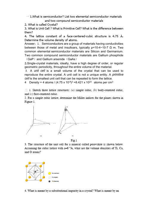
一1.What is semiconductor? List two elemental semiconductor materials and two compound semiconductor materials2. What is called Crystal?3. What is Unit Cell ? What is Primitive Cell? What is the difference between them?4. The lattice constant of a face-centered-cubic structure is 4.75 Å. Determine the volume density of atoms.Answer:1. Semiconductors are a group of materials having conductivities between those of metal and insultoars, typically ρ=10-4~10-7 Ω m. Two common elemental semiconductor materials are Silicon and Germanium. Two common compound semiconductor materials are Gallium phosphide (GaP)and Gallium arsenide(GaAs)2.Single-crystal materials, ideally, have a high degree of order, or regular geometric periodicity, throughout the entire volume of the material.3. A unit cell is a small volume of the crystal that can be used to reproduce the entire crystal. A unit cell is not a unique entity. A primitive cell is the smallest unit cell that can be repeated to form the lattice.4 Density = 4 atoms / (4.75 x 10⁻⁸)3 =8.421 x 10²³atoms per cm3二1. Sketch three lattice structures: (a) simple cubic, (b) body-centered cubic, and (c) face-centered cubic.2. For a simple cubic lattice, determine the Miller indices for the planes shown in Figure 1.Fig.13. The structure of the unit cell for a mineral called perovskite is shown below. Assuming the cubic lattice with a=6 °A, what are the volume densities of Ti, Ca, and O atoms?4. What is meant by a substitutional impurity in a crystal? What is meant by anintcrstilial impurity?2. left:(313) ; right:(121)3. solution: Density (Ca)= 881⨯atoms / a 3 = 4.63 x 10²¹ atoms per cm 3 Density (O)=216⨯ atoms / a 3 =1.39 x 10²² atoms per cm 3 Density (Ti)=1/a 3 = 4.63 x 10²¹ atoms per cm 3三 1. Ultraviolet light (紫外光) of wavelength 150nm falls on a chromium [/kr əʊmi:əm] (铬Cr) electrode(电极). Calculate the maximum kinetic energy and the corresponding velocity of the photoelectrons (the work function of chromium is4.37eV).2. Calculate the photon energies for the following types of electromagnetic radiation: (a) a 600kHz radio wave; (b) the 500nm (wavelength of) green light; (c) a 0.1 nm (wavelength of) X-rays.1、Solution: using the equation of the photoelectric effect, it is convenient to express the energy in electron volts. The photon energy isSolution:(a) for the radio wave, we can use the Planck-Einstein law directly(b) The light wave is specified by wavelength, we can use the law explained in wavelength:四 1 Determine the energy of a photon having wavelengths of (a) λ = 10,000Ǻ and (b) λ= 10Ǻ.2 (a) Find the momentum and energy of a particle with mass of 5 x10-31 kg and a de Broglie wavelength of 180Ǻ. (b) An electron has a kinetic energy of 20 meV . Determine the de Broglie wavelength.eV Hz s eV h E 93151048.21060010136.4--⨯=⨯⨯⋅⨯==ν1、(a) 1.99 x10⁻¹⁹J or 1.24eV. (b) 1.99 x10⁻¹⁶J or 1.24x10³eV2、(a) p=3.68 x10⁻²⁶kgm/s, E=1.35 x10⁻²¹J or 8.46 x10⁻³eV. (b) p=7.64 x10⁻²⁶kgm/s , λ= 86.7Ǻ五E2.5 The width of the infinite potential well in Example 2.3 is doubled to 10Ǻ. Calculatethe first three energy levels in terms of electron volts for an electron.E2.6 The lowest energy of a particle in an infinite potential well with a width of 100 Ǻ is0.025 eV. What is the mass of the particle?1、Ans. 0.376eV, 1.50eV, 3.38eV2、Ans. 1.37X10⁻³¹kg六1. What is the Kronig-Penney model ?2. Discuss the concept of allowed and forbidden energy bands in a single crystal qualitatively with your classmate.3. Discuss the splitting of energy bands in silicon with your classmate.4. (a) If 2X10¹⁶boron atoms per cm3are added to silicon as a substitutional impurity, determine what percentage of the silicon atoms and displayed in the single crystal lattice. (b) repeat part (a) for 1015 boron atoms per cm3. (课本P45)5. If 2X10¹⁵ gold atoms per cm3 are added to silicon as a substitutional impurity and are distributed uniformly throughout the semiconductor, determine the distance between gold atoms in terms of the silicon lattice constant. (Assume the gold atoms are distributed in a rectangular or cubic array.) (课本P45)七3.1Consider Figure 3.4b. which shows the energy-band splitting of silicon. Ifthe equilibrium lattice spacing were to change by a small amount. discusshow you would expect the electrical properties of silicon to change.Determine at what point the material would behave like an insulator or likea metal.3.2Show that Equations (3.4) and (3.6) are derived from Schrodinger's waveequation. using the fom~o f solution given by Equation (3.3).3.3Show that Equations (3.9) and (3.10) are solutions of the differentialequations given by Equations (3.4) and (3.8). respectively.3.4 Show that Equations (3.12) (3.14), (3.16). and (3.18) rcsult from theboundary conditions in the Kronig-Penney model.这四道题在课本第98页. 八For the electron near the top of the allowed energy band (see Figure 3.16b), show that it behaves as if it has a negative mass.(Refer to textbook pp77-78)2. p99,3.13-3.153. p45, E2.10 (selective)九Answer the questions:1. What is effective mass?2. What is a direct bandgap semiconductor? What is an indirect bandgap semiconductor?3. What is the meaning of the density of states function?4. What was the mathematical model used in deriving the density of states function?5. In general, what is the relation between density of states and energy? Problems:P1003.20, 3.22十3.13 m*(A)<m*(B)3.15 A, B: velocity =-x : C, D: velocity = +x;B. C: positive mass; A, D: negative mass19.3 Å十一Answer the questions1. In general, what is the relation between density of states and energy?2. What is the meaning of the Fermi-Dirac probability function?3. What is the Fermi energy?Problem:1.3P85, Example 3.32. Consider the density of states for a free electron given by Equation (3.69). Calculate the density of states per unit volume with energies between 0 and 2eV.3. To determine the possible number of ways of realizing a particular distribution. Let gi = 10 and Ni =8.4. Calculate the temperature at which there is a 10-6 probability that an energy state 0.55 eV above the Fermi energy level is occupied by an electron.十二Questions:1. Assuming the Boltzmann approximation applies, write the equations for n0 and p0 in terms of the Fermi energy.2. What is the value of the intrinsic carrier concentration in silicon at T = 300 K?3. Under what condition would the intrinsic Fermi level be at the midgap energy? Problems:P148,4.1, 4.2, 4.8, 4.12十三Questions:1. What is intrinsic semiconductor? What is extrinsic semiconductor? Why the extrinsic semiconductor is more useful than the intrinsic semiconductor?2. What is ionization energy? Why the resistance of the extrinsic semiconductor is quite sensitive to doping?Problems:1. Calculate the ionization energy of the hydrogen atom using Bohr theory.(-13.6eV)2. Calculate the ionization energy of the donor electron in silicon using Bohr theory. (for silicon, =1.17, =0.26). (-25.8meV)十四 P147, review questions, 7,8,10,11P149, 4.19, 4.21r *0/m m。
半导体器件机理 英文
半导体器件机理英文Semiconductor Device Mechanisms.Semiconductors are materials that have electrical conductivity between that of a conductor and an insulator. This unique property makes them essential for a wide range of electronic devices, including transistors, diodes, and solar cells.The electrical properties of semiconductors are determined by their electronic band structure. In a semiconductor, the valence band is the highest energy band that is occupied by electrons, while the conduction band is the lowest energy band that is unoccupied. The band gap is the energy difference between the valence band and the conduction band.At room temperature, most semiconductors have a relatively large band gap, which means that there are very few electrons in the conduction band. This makessemiconductors poor conductors of electricity. However, the electrical conductivity of a semiconductor can be increased by doping it with impurities.Donor impurities are atoms that have one more valence electron than the semiconductor atoms they replace. When a donor impurity is added to a semiconductor, the extra electron is donated to the conduction band, increasing the number of charge carriers and the electrical conductivityof the semiconductor.Acceptor impurities are atoms that have one lessvalence electron than the semiconductor atoms they replace. When an acceptor impurity is added to a semiconductor, the missing electron creates a hole in the valence band. Holes are positively charged, and they can move through the semiconductor by accepting electrons from neighboring atoms. This also increases the electrical conductivity of the semiconductor.The type of impurity that is added to a semiconductor determines whether it becomes an n-type semiconductor (witha majority of electrons as charge carriers) or a p-type semiconductor (with a majority of holes as charge carriers).The combination of n-type and p-type semiconductors is used to create a wide range of electronic devices,including transistors, diodes, and solar cells.Transistors.Transistors are three-terminal devices that can be used to amplify or switch electronic signals. The threeterminals are the emitter, the base, and the collector.In a bipolar junction transistor (BJT), the emitter is an n-type semiconductor, the base is a p-type semiconductor, and the collector is another n-type semiconductor. When a small current is applied to the base, it causes a large current to flow between the emitter and the collector. This makes BJTs ideal for use as amplifiers.In a field-effect transistor (FET), the gate is a metal electrode that is insulated from the channel. When avoltage is applied to the gate, it creates an electricfield that attracts or repels electrons in the channel. This changes the conductivity of the channel, which in turn controls the flow of current between the source and the drain. FETs are ideal for use as switches.Diodes.Diodes are two-terminal devices that allow current to flow in only one direction. The two terminals are the anode and the cathode.In a p-n diode, the anode is a p-type semiconductor and the cathode is an n-type semiconductor. When a voltage is applied to the diode, it causes electrons to flow from the n-type semiconductor to the p-type semiconductor, but not vice versa. This makes diodes ideal for use as rectifiers, which convert alternating current (AC) to direct current (DC).Solar Cells.Solar cells are devices that convert light energy into electrical energy. They are made of a semiconductor material, such as silicon, that has a p-n junction.When light strikes the solar cell, it creates electron-hole pairs in the semiconductor. The electrons areattracted to the n-type semiconductor, while the holes are attracted to the p-type semiconductor. This creates a voltage difference between the two semiconductors, which causes current to flow.Solar cells are used to power a wide range of devices, including calculators, watches, and satellites. They are also used to generate electricity for homes and businesses.Conclusion.Semiconductors are essential for a wide range of electronic devices. Their unique electrical properties make them ideal for use in transistors, diodes, and solar cells. As semiconductor technology continues to develop, we canexpect to see even more innovative and efficient electronic devices in the future.。
物理学专业英语

华中师范大学物理学院物理学专业英语仅供内部学习参考!2014一、课程的任务和教学目的通过学习《物理学专业英语》,学生将掌握物理学领域使用频率较高的专业词汇和表达方法,进而具备基本的阅读理解物理学专业文献的能力。
通过分析《物理学专业英语》课程教材中的范文,学生还将从英语角度理解物理学中个学科的研究内容和主要思想,提高学生的专业英语能力和了解物理学研究前沿的能力。
培养专业英语阅读能力,了解科技英语的特点,提高专业外语的阅读质量和阅读速度;掌握一定量的本专业英文词汇,基本达到能够独立完成一般性本专业外文资料的阅读;达到一定的笔译水平。
要求译文通顺、准确和专业化。
要求译文通顺、准确和专业化。
二、课程内容课程内容包括以下章节:物理学、经典力学、热力学、电磁学、光学、原子物理、统计力学、量子力学和狭义相对论三、基本要求1.充分利用课内时间保证充足的阅读量(约1200~1500词/学时),要求正确理解原文。
2.泛读适量课外相关英文读物,要求基本理解原文主要内容。
3.掌握基本专业词汇(不少于200词)。
4.应具有流利阅读、翻译及赏析专业英语文献,并能简单地进行写作的能力。
四、参考书目录1 Physics 物理学 (1)Introduction to physics (1)Classical and modern physics (2)Research fields (4)V ocabulary (7)2 Classical mechanics 经典力学 (10)Introduction (10)Description of classical mechanics (10)Momentum and collisions (14)Angular momentum (15)V ocabulary (16)3 Thermodynamics 热力学 (18)Introduction (18)Laws of thermodynamics (21)System models (22)Thermodynamic processes (27)Scope of thermodynamics (29)V ocabulary (30)4 Electromagnetism 电磁学 (33)Introduction (33)Electrostatics (33)Magnetostatics (35)Electromagnetic induction (40)V ocabulary (43)5 Optics 光学 (45)Introduction (45)Geometrical optics (45)Physical optics (47)Polarization (50)V ocabulary (51)6 Atomic physics 原子物理 (52)Introduction (52)Electronic configuration (52)Excitation and ionization (56)V ocabulary (59)7 Statistical mechanics 统计力学 (60)Overview (60)Fundamentals (60)Statistical ensembles (63)V ocabulary (65)8 Quantum mechanics 量子力学 (67)Introduction (67)Mathematical formulations (68)Quantization (71)Wave-particle duality (72)Quantum entanglement (75)V ocabulary (77)9 Special relativity 狭义相对论 (79)Introduction (79)Relativity of simultaneity (80)Lorentz transformations (80)Time dilation and length contraction (81)Mass-energy equivalence (82)Relativistic energy-momentum relation (86)V ocabulary (89)正文标记说明:蓝色Arial字体(例如energy):已知的专业词汇蓝色Arial字体加下划线(例如electromagnetism):新学的专业词汇黑色Times New Roman字体加下划线(例如postulate):新学的普通词汇1 Physics 物理学1 Physics 物理学Introduction to physicsPhysics is a part of natural philosophy and a natural science that involves the study of matter and its motion through space and time, along with related concepts such as energy and force. More broadly, it is the general analysis of nature, conducted in order to understand how the universe behaves.Physics is one of the oldest academic disciplines, perhaps the oldest through its inclusion of astronomy. Over the last two millennia, physics was a part of natural philosophy along with chemistry, certain branches of mathematics, and biology, but during the Scientific Revolution in the 17th century, the natural sciences emerged as unique research programs in their own right. Physics intersects with many interdisciplinary areas of research, such as biophysics and quantum chemistry,and the boundaries of physics are not rigidly defined. New ideas in physics often explain the fundamental mechanisms of other sciences, while opening new avenues of research in areas such as mathematics and philosophy.Physics also makes significant contributions through advances in new technologies that arise from theoretical breakthroughs. For example, advances in the understanding of electromagnetism or nuclear physics led directly to the development of new products which have dramatically transformed modern-day society, such as television, computers, domestic appliances, and nuclear weapons; advances in thermodynamics led to the development of industrialization; and advances in mechanics inspired the development of calculus.Core theoriesThough physics deals with a wide variety of systems, certain theories are used by all physicists. Each of these theories were experimentally tested numerous times and found correct as an approximation of nature (within a certain domain of validity).For instance, the theory of classical mechanics accurately describes the motion of objects, provided they are much larger than atoms and moving at much less than the speed of light. These theories continue to be areas of active research, and a remarkable aspect of classical mechanics known as chaos was discovered in the 20th century, three centuries after the original formulation of classical mechanics by Isaac Newton (1642–1727) 【艾萨克·牛顿】.University PhysicsThese central theories are important tools for research into more specialized topics, and any physicist, regardless of his or her specialization, is expected to be literate in them. These include classical mechanics, quantum mechanics, thermodynamics and statistical mechanics, electromagnetism, and special relativity.Classical and modern physicsClassical mechanicsClassical physics includes the traditional branches and topics that were recognized and well-developed before the beginning of the 20th century—classical mechanics, acoustics, optics, thermodynamics, and electromagnetism.Classical mechanics is concerned with bodies acted on by forces and bodies in motion and may be divided into statics (study of the forces on a body or bodies at rest), kinematics (study of motion without regard to its causes), and dynamics (study of motion and the forces that affect it); mechanics may also be divided into solid mechanics and fluid mechanics (known together as continuum mechanics), the latter including such branches as hydrostatics, hydrodynamics, aerodynamics, and pneumatics.Acoustics is the study of how sound is produced, controlled, transmitted and received. Important modern branches of acoustics include ultrasonics, the study of sound waves of very high frequency beyond the range of human hearing; bioacoustics the physics of animal calls and hearing, and electroacoustics, the manipulation of audible sound waves using electronics.Optics, the study of light, is concerned not only with visible light but also with infrared and ultraviolet radiation, which exhibit all of the phenomena of visible light except visibility, e.g., reflection, refraction, interference, diffraction, dispersion, and polarization of light.Heat is a form of energy, the internal energy possessed by the particles of which a substance is composed; thermodynamics deals with the relationships between heat and other forms of energy.Electricity and magnetism have been studied as a single branch of physics since the intimate connection between them was discovered in the early 19th century; an electric current gives rise to a magnetic field and a changing magnetic field induces an electric current. Electrostatics deals with electric charges at rest, electrodynamics with moving charges, and magnetostatics with magnetic poles at rest.Modern PhysicsClassical physics is generally concerned with matter and energy on the normal scale of1 Physics 物理学observation, while much of modern physics is concerned with the behavior of matter and energy under extreme conditions or on the very large or very small scale.For example, atomic and nuclear physics studies matter on the smallest scale at which chemical elements can be identified.The physics of elementary particles is on an even smaller scale, as it is concerned with the most basic units of matter; this branch of physics is also known as high-energy physics because of the extremely high energies necessary to produce many types of particles in large particle accelerators. On this scale, ordinary, commonsense notions of space, time, matter, and energy are no longer valid.The two chief theories of modern physics present a different picture of the concepts of space, time, and matter from that presented by classical physics.Quantum theory is concerned with the discrete, rather than continuous, nature of many phenomena at the atomic and subatomic level, and with the complementary aspects of particles and waves in the description of such phenomena.The theory of relativity is concerned with the description of phenomena that take place in a frame of reference that is in motion with respect to an observer; the special theory of relativity is concerned with relative uniform motion in a straight line and the general theory of relativity with accelerated motion and its connection with gravitation.Both quantum theory and the theory of relativity find applications in all areas of modern physics.Difference between classical and modern physicsWhile physics aims to discover universal laws, its theories lie in explicit domains of applicability. Loosely speaking, the laws of classical physics accurately describe systems whose important length scales are greater than the atomic scale and whose motions are much slower than the speed of light. Outside of this domain, observations do not match their predictions.Albert Einstein【阿尔伯特·爱因斯坦】contributed the framework of special relativity, which replaced notions of absolute time and space with space-time and allowed an accurate description of systems whose components have speeds approaching the speed of light.Max Planck【普朗克】, Erwin Schrödinger【薛定谔】, and others introduced quantum mechanics, a probabilistic notion of particles and interactions that allowed an accurate description of atomic and subatomic scales.Later, quantum field theory unified quantum mechanics and special relativity.General relativity allowed for a dynamical, curved space-time, with which highly massiveUniversity Physicssystems and the large-scale structure of the universe can be well-described. General relativity has not yet been unified with the other fundamental descriptions; several candidate theories of quantum gravity are being developed.Research fieldsContemporary research in physics can be broadly divided into condensed matter physics; atomic, molecular, and optical physics; particle physics; astrophysics; geophysics and biophysics. Some physics departments also support research in Physics education.Since the 20th century, the individual fields of physics have become increasingly specialized, and today most physicists work in a single field for their entire careers. "Universalists" such as Albert Einstein (1879–1955) and Lev Landau (1908–1968)【列夫·朗道】, who worked in multiple fields of physics, are now very rare.Condensed matter physicsCondensed matter physics is the field of physics that deals with the macroscopic physical properties of matter. In particular, it is concerned with the "condensed" phases that appear whenever the number of particles in a system is extremely large and the interactions between them are strong.The most familiar examples of condensed phases are solids and liquids, which arise from the bonding by way of the electromagnetic force between atoms. More exotic condensed phases include the super-fluid and the Bose–Einstein condensate found in certain atomic systems at very low temperature, the superconducting phase exhibited by conduction electrons in certain materials,and the ferromagnetic and antiferromagnetic phases of spins on atomic lattices.Condensed matter physics is by far the largest field of contemporary physics.Historically, condensed matter physics grew out of solid-state physics, which is now considered one of its main subfields. The term condensed matter physics was apparently coined by Philip Anderson when he renamed his research group—previously solid-state theory—in 1967. In 1978, the Division of Solid State Physics of the American Physical Society was renamed as the Division of Condensed Matter Physics.Condensed matter physics has a large overlap with chemistry, materials science, nanotechnology and engineering.Atomic, molecular and optical physicsAtomic, molecular, and optical physics (AMO) is the study of matter–matter and light–matter interactions on the scale of single atoms and molecules.1 Physics 物理学The three areas are grouped together because of their interrelationships, the similarity of methods used, and the commonality of the energy scales that are relevant. All three areas include both classical, semi-classical and quantum treatments; they can treat their subject from a microscopic view (in contrast to a macroscopic view).Atomic physics studies the electron shells of atoms. Current research focuses on activities in quantum control, cooling and trapping of atoms and ions, low-temperature collision dynamics and the effects of electron correlation on structure and dynamics. Atomic physics is influenced by the nucleus (see, e.g., hyperfine splitting), but intra-nuclear phenomena such as fission and fusion are considered part of high-energy physics.Molecular physics focuses on multi-atomic structures and their internal and external interactions with matter and light.Optical physics is distinct from optics in that it tends to focus not on the control of classical light fields by macroscopic objects, but on the fundamental properties of optical fields and their interactions with matter in the microscopic realm.High-energy physics (particle physics) and nuclear physicsParticle physics is the study of the elementary constituents of matter and energy, and the interactions between them.In addition, particle physicists design and develop the high energy accelerators,detectors, and computer programs necessary for this research. The field is also called "high-energy physics" because many elementary particles do not occur naturally, but are created only during high-energy collisions of other particles.Currently, the interactions of elementary particles and fields are described by the Standard Model.●The model accounts for the 12 known particles of matter (quarks and leptons) thatinteract via the strong, weak, and electromagnetic fundamental forces.●Dynamics are described in terms of matter particles exchanging gauge bosons (gluons,W and Z bosons, and photons, respectively).●The Standard Model also predicts a particle known as the Higgs boson. In July 2012CERN, the European laboratory for particle physics, announced the detection of a particle consistent with the Higgs boson.Nuclear Physics is the field of physics that studies the constituents and interactions of atomic nuclei. The most commonly known applications of nuclear physics are nuclear power generation and nuclear weapons technology, but the research has provided application in many fields, including those in nuclear medicine and magnetic resonance imaging, ion implantation in materials engineering, and radiocarbon dating in geology and archaeology.University PhysicsAstrophysics and Physical CosmologyAstrophysics and astronomy are the application of the theories and methods of physics to the study of stellar structure, stellar evolution, the origin of the solar system, and related problems of cosmology. Because astrophysics is a broad subject, astrophysicists typically apply many disciplines of physics, including mechanics, electromagnetism, statistical mechanics, thermodynamics, quantum mechanics, relativity, nuclear and particle physics, and atomic and molecular physics.The discovery by Karl Jansky in 1931 that radio signals were emitted by celestial bodies initiated the science of radio astronomy. Most recently, the frontiers of astronomy have been expanded by space exploration. Perturbations and interference from the earth's atmosphere make space-based observations necessary for infrared, ultraviolet, gamma-ray, and X-ray astronomy.Physical cosmology is the study of the formation and evolution of the universe on its largest scales. Albert Einstein's theory of relativity plays a central role in all modern cosmological theories. In the early 20th century, Hubble's discovery that the universe was expanding, as shown by the Hubble diagram, prompted rival explanations known as the steady state universe and the Big Bang.The Big Bang was confirmed by the success of Big Bang nucleo-synthesis and the discovery of the cosmic microwave background in 1964. The Big Bang model rests on two theoretical pillars: Albert Einstein's general relativity and the cosmological principle (On a sufficiently large scale, the properties of the Universe are the same for all observers). Cosmologists have recently established the ΛCDM model (the standard model of Big Bang cosmology) of the evolution of the universe, which includes cosmic inflation, dark energy and dark matter.Current research frontiersIn condensed matter physics, an important unsolved theoretical problem is that of high-temperature superconductivity. Many condensed matter experiments are aiming to fabricate workable spintronics and quantum computers.In particle physics, the first pieces of experimental evidence for physics beyond the Standard Model have begun to appear. Foremost among these are indications that neutrinos have non-zero mass. These experimental results appear to have solved the long-standing solar neutrino problem, and the physics of massive neutrinos remains an area of active theoretical and experimental research. Particle accelerators have begun probing energy scales in the TeV range, in which experimentalists are hoping to find evidence for the super-symmetric particles, after discovery of the Higgs boson.Theoretical attempts to unify quantum mechanics and general relativity into a single theory1 Physics 物理学of quantum gravity, a program ongoing for over half a century, have not yet been decisively resolved. The current leading candidates are M-theory, superstring theory and loop quantum gravity.Many astronomical and cosmological phenomena have yet to be satisfactorily explained, including the existence of ultra-high energy cosmic rays, the baryon asymmetry, the acceleration of the universe and the anomalous rotation rates of galaxies.Although much progress has been made in high-energy, quantum, and astronomical physics, many everyday phenomena involving complexity, chaos, or turbulence are still poorly understood. Complex problems that seem like they could be solved by a clever application of dynamics and mechanics remain unsolved; examples include the formation of sand-piles, nodes in trickling water, the shape of water droplets, mechanisms of surface tension catastrophes, and self-sorting in shaken heterogeneous collections.These complex phenomena have received growing attention since the 1970s for several reasons, including the availability of modern mathematical methods and computers, which enabled complex systems to be modeled in new ways. Complex physics has become part of increasingly interdisciplinary research, as exemplified by the study of turbulence in aerodynamics and the observation of pattern formation in biological systems.Vocabulary★natural science 自然科学academic disciplines 学科astronomy 天文学in their own right 凭他们本身的实力intersects相交,交叉interdisciplinary交叉学科的,跨学科的★quantum 量子的theoretical breakthroughs 理论突破★electromagnetism 电磁学dramatically显著地★thermodynamics热力学★calculus微积分validity★classical mechanics 经典力学chaos 混沌literate 学者★quantum mechanics量子力学★thermodynamics and statistical mechanics热力学与统计物理★special relativity狭义相对论is concerned with 关注,讨论,考虑acoustics 声学★optics 光学statics静力学at rest 静息kinematics运动学★dynamics动力学ultrasonics超声学manipulation 操作,处理,使用University Physicsinfrared红外ultraviolet紫外radiation辐射reflection 反射refraction 折射★interference 干涉★diffraction 衍射dispersion散射★polarization 极化,偏振internal energy 内能Electricity电性Magnetism 磁性intimate 亲密的induces 诱导,感应scale尺度★elementary particles基本粒子★high-energy physics 高能物理particle accelerators 粒子加速器valid 有效的,正当的★discrete离散的continuous 连续的complementary 互补的★frame of reference 参照系★the special theory of relativity 狭义相对论★general theory of relativity 广义相对论gravitation 重力,万有引力explicit 详细的,清楚的★quantum field theory 量子场论★condensed matter physics凝聚态物理astrophysics天体物理geophysics地球物理Universalist博学多才者★Macroscopic宏观Exotic奇异的★Superconducting 超导Ferromagnetic铁磁质Antiferromagnetic 反铁磁质★Spin自旋Lattice 晶格,点阵,网格★Society社会,学会★microscopic微观的hyperfine splitting超精细分裂fission分裂,裂变fusion熔合,聚变constituents成分,组分accelerators加速器detectors 检测器★quarks夸克lepton 轻子gauge bosons规范玻色子gluons胶子★Higgs boson希格斯玻色子CERN欧洲核子研究中心★Magnetic Resonance Imaging磁共振成像,核磁共振ion implantation 离子注入radiocarbon dating放射性碳年代测定法geology地质学archaeology考古学stellar 恒星cosmology宇宙论celestial bodies 天体Hubble diagram 哈勃图Rival竞争的★Big Bang大爆炸nucleo-synthesis核聚合,核合成pillar支柱cosmological principle宇宙学原理ΛCDM modelΛ-冷暗物质模型cosmic inflation宇宙膨胀1 Physics 物理学fabricate制造,建造spintronics自旋电子元件,自旋电子学★neutrinos 中微子superstring 超弦baryon重子turbulence湍流,扰动,骚动catastrophes突变,灾变,灾难heterogeneous collections异质性集合pattern formation模式形成University Physics2 Classical mechanics 经典力学IntroductionIn physics, classical mechanics is one of the two major sub-fields of mechanics, which is concerned with the set of physical laws describing the motion of bodies under the action of a system of forces. The study of the motion of bodies is an ancient one, making classical mechanics one of the oldest and largest subjects in science, engineering and technology.Classical mechanics describes the motion of macroscopic objects, from projectiles to parts of machinery, as well as astronomical objects, such as spacecraft, planets, stars, and galaxies. Besides this, many specializations within the subject deal with gases, liquids, solids, and other specific sub-topics.Classical mechanics provides extremely accurate results as long as the domain of study is restricted to large objects and the speeds involved do not approach the speed of light. When the objects being dealt with become sufficiently small, it becomes necessary to introduce the other major sub-field of mechanics, quantum mechanics, which reconciles the macroscopic laws of physics with the atomic nature of matter and handles the wave–particle duality of atoms and molecules. In the case of high velocity objects approaching the speed of light, classical mechanics is enhanced by special relativity. General relativity unifies special relativity with Newton's law of universal gravitation, allowing physicists to handle gravitation at a deeper level.The initial stage in the development of classical mechanics is often referred to as Newtonian mechanics, and is associated with the physical concepts employed by and the mathematical methods invented by Newton himself, in parallel with Leibniz【莱布尼兹】, and others.Later, more abstract and general methods were developed, leading to reformulations of classical mechanics known as Lagrangian mechanics and Hamiltonian mechanics. These advances were largely made in the 18th and 19th centuries, and they extend substantially beyond Newton's work, particularly through their use of analytical mechanics. Ultimately, the mathematics developed for these were central to the creation of quantum mechanics.Description of classical mechanicsThe following introduces the basic concepts of classical mechanics. For simplicity, it often2 Classical mechanics 经典力学models real-world objects as point particles, objects with negligible size. The motion of a point particle is characterized by a small number of parameters: its position, mass, and the forces applied to it.In reality, the kind of objects that classical mechanics can describe always have a non-zero size. (The physics of very small particles, such as the electron, is more accurately described by quantum mechanics). Objects with non-zero size have more complicated behavior than hypothetical point particles, because of the additional degrees of freedom—for example, a baseball can spin while it is moving. However, the results for point particles can be used to study such objects by treating them as composite objects, made up of a large number of interacting point particles. The center of mass of a composite object behaves like a point particle.Classical mechanics uses common-sense notions of how matter and forces exist and interact. It assumes that matter and energy have definite, knowable attributes such as where an object is in space and its speed. It also assumes that objects may be directly influenced only by their immediate surroundings, known as the principle of locality.In quantum mechanics objects may have unknowable position or velocity, or instantaneously interact with other objects at a distance.Position and its derivativesThe position of a point particle is defined with respect to an arbitrary fixed reference point, O, in space, usually accompanied by a coordinate system, with the reference point located at the origin of the coordinate system. It is defined as the vector r from O to the particle.In general, the point particle need not be stationary relative to O, so r is a function of t, the time elapsed since an arbitrary initial time.In pre-Einstein relativity (known as Galilean relativity), time is considered an absolute, i.e., the time interval between any given pair of events is the same for all observers. In addition to relying on absolute time, classical mechanics assumes Euclidean geometry for the structure of space.Velocity and speedThe velocity, or the rate of change of position with time, is defined as the derivative of the position with respect to time. In classical mechanics, velocities are directly additive and subtractive as vector quantities; they must be dealt with using vector analysis.When both objects are moving in the same direction, the difference can be given in terms of speed only by ignoring direction.University PhysicsAccelerationThe acceleration , or rate of change of velocity, is the derivative of the velocity with respect to time (the second derivative of the position with respect to time).Acceleration can arise from a change with time of the magnitude of the velocity or of the direction of the velocity or both . If only the magnitude v of the velocity decreases, this is sometimes referred to as deceleration , but generally any change in the velocity with time, including deceleration, is simply referred to as acceleration.Inertial frames of referenceWhile the position and velocity and acceleration of a particle can be referred to any observer in any state of motion, classical mechanics assumes the existence of a special family of reference frames in terms of which the mechanical laws of nature take a comparatively simple form. These special reference frames are called inertial frames .An inertial frame is such that when an object without any force interactions (an idealized situation) is viewed from it, it appears either to be at rest or in a state of uniform motion in a straight line. This is the fundamental definition of an inertial frame. They are characterized by the requirement that all forces entering the observer's physical laws originate in identifiable sources (charges, gravitational bodies, and so forth).A non-inertial reference frame is one accelerating with respect to an inertial one, and in such a non-inertial frame a particle is subject to acceleration by fictitious forces that enter the equations of motion solely as a result of its accelerated motion, and do not originate in identifiable sources. These fictitious forces are in addition to the real forces recognized in an inertial frame.A key concept of inertial frames is the method for identifying them. For practical purposes, reference frames that are un-accelerated with respect to the distant stars are regarded as good approximations to inertial frames.Forces; Newton's second lawNewton was the first to mathematically express the relationship between force and momentum . Some physicists interpret Newton's second law of motion as a definition of force and mass, while others consider it a fundamental postulate, a law of nature. Either interpretation has the same mathematical consequences, historically known as "Newton's Second Law":a m t v m t p F ===d )(d d dThe quantity m v is called the (canonical ) momentum . The net force on a particle is thus equal to rate of change of momentum of the particle with time.So long as the force acting on a particle is known, Newton's second law is sufficient to。
Early photon-shock interaction in stellar wind sub-GeV photon flash and high energy neutrin
overlapping effect in the wind model. In §3 we show that such an early photon-shock interaction inevitably leads to the prediction of a sub-GeV photon flash in the wind model, which is generally detectable by the Gamma-Ray Large Area Telescope (GLAST). In §4, we discuss various high energy neutrino emission processes in the early afterglow stage as the result of photon-shock interaction. We summarize our conclusions in §5 with some discussions.
Accepted for publication in ApJ
A Preprint typeset using L TEX style emulateapj v. 6/22/04
EARLY PHOTON-SHOCK INTERACTION IN A STELLAR WIND: A SUB-GEV PHOTON FLASH AND HIGH ENERGY NEUTRINO EMISSION FROM LONG GRBS
2
1
Accepted for publication in ApJ
arXiv:astro-ph/0504039v3 9 Jun 2005
ABSTRACT For gamma-ray bursts (GRBs) born in a stellar wind, as the reverse shock crosses the ejecta, usually the shocked regions are still precipitated by the prompt MeV γ −ray emission. Because of the tight overlapping of the MeV photon flow with the shocked regions, the optical depth for the GeV photons produced in the shocks is very large. These high energy photons are absorbed by the MeV photon flow and generate relativistic e± pairs. These pairs re-scatter the soft X-ray photons from the forward shock as well as the prompt γ −ray photons and power detectable high energy emission, significant part of which is in the sub-GeV energy range. Since the total energy contained in the forward shock region and the reverse shock region are comparable, the predicted sub-GeV emission is independent on whether the GRB ejecta are magnetized (in which case the reverse shock IC and synchrotron selfCompton emission is suppressed). As a result, a sub-GeV flash is a generic signature for the GRB wind model, and it should be typically detectable by the future Gamma-Ray Large Area Telescope (GLAST). Overlapping also influence neutrino emission. Besides the 1015 ∼ 1017 eV neutrino emission powered by the interaction of the shock accelerated protons with the synchrotron photons in both the forward and reverse shock regions, there comes another 1014 eV neutrino emission component powered by protons interacting with the MeV photon flow. This last component has a similar spectrum to the one generated in the internal shock phase, but the typical energy is slightly lower. Subject headings: gamma rays: bursts - acceleration of particles - elementary particles
2007自然杂志石墨烯诺贝尔得奖者文章
THE RISE OF GRAPHENEA.K. Geim and K.S. NovoselovManchester Centre for Mesoscience and Nanotechnology,University of Manchester, Oxford Road M13 9PL, United KingdomGraphene is a rapidly rising star on the horizon of materials science and condensed matter physics. This strictly two-dimensional material exhibits exceptionally high crystal and electronic quality and, despite its short history, has already revealed a cornucopia of new physics and potential applications, which are briefly discussed here. Whereas one can be certain of the realness of applications only when commercial products appear, graphene no longer requires any further proof of its importance in terms of fundamental physics. Owing to its unusual electronic spectrum, graphene has led to the emergence of a new paradigm of “relativistic” condensed matter physics, where quantum relativistic phenomena, some of which are unobservable in high energy physics, can now be mimicked and tested in table-top experiments. More generally, graphene represents a conceptually new class of materials that are only one atom thick and, on this basis, offers new inroads into low-dimensional physics that has never ceased to surprise and continues to provide a fertile ground for applications.Graphene is the name given to a flat monolayer of carbon atoms tightly packed into a two-dimensional (2D) honeycomb lattice, and is a basic building block for graphitic materials of all other dimensionalities (Figure 1). It can be wrapped up into 0D fullerenes, rolled into 1D nanotubes or stacked into 3D graphite. Theoretically, graphene (or “2D graphite”) has been studied for sixty years1-3 and widely used for describing properties of various carbon-based materials. Forty years later, it was realized that graphene also provides an excellent condensed-matter analogue of (2+1)-dimensional quantum electrodynamics4-6, which propelled graphene into a thriving theoretical toy model. On the other hand, although known as integral part of 3D materials, graphene was presumed not to exist in the free state, being described as an “academic” material5 and believed to be unstable with respect to the formation of curved structures such as soot, fullerenes and nanotubes. All of a sudden, the vintage model turned into reality, when free-standing graphene was unexpectedly found three years ago7,8 and, especially, when the follow-up experiments9,10 confirmed that its charge carriers were indeed massless Dirac fermions. So, the graphene “gold rush” has begun.MATERIALS THAT SHOULD NOT EXISTMore than 70 years ago, Landau and Peierls argued that strictly two-dimensional (2D) crystals were thermodynamically unstable and could not exist11,12. Their theory pointed out that a divergent contribution of thermal fluctuations in low-dimensional crystal lattices should lead to such displacements of atoms that they become comparable to interatomic distances at any finite temperature13. The argument was later extended by Mermin14 and is strongly supported by a whole omnibus of experimental observations. Indeed, the melting temperature of thin films rapidly decreases with decreasing thickness, and they become unstable (segregate into islands or decompose) at a thickness of, typically, dozens of atomic layers15,16. For this reason, atomic monolayers have so far been known only as an integral part of larger 3D structures, usually grown epitaxially on top of monocrystals with matching crystal lattices15,16. Without such a 3D base, 2D materials were presumed not to exist until 2004, when the common wisdom was flaunted by the experimental discovery of graphene7 and other free-standing 2D atomic crystals (for example, single-layer boron nitride and half-layer BSCCO)8. These crystals could be obtained on top of non-crystalline substrates8-10, in liquid suspension7,17 and as suspended membranes18.Importantly, the 2D crystals were found not only to be continuous but to exhibit high crystal quality7-10,17,18. The latter is most obvious for the case of graphene, in which charge carriers can travel thousands interatomic distances without scattering7-10. With the benefit of hindsight, the existence of such one-atom-thick crystals can be reconciled with theory. Indeed, it can be argued that the obtained 2D crystallites are quenched in a metastable state because they are extracted from 3D materials, whereas their small size (<<1mm) and strong interatomic bonds assure that thermal fluctuations cannot lead to the generation of dislocations or other crystal defects even at elevated temperature13,14.Figure 1. Mother of all graphitic forms. Graphene is a 2D building material for carbon materials of all other dimensionalities. It can be wrapped up into 0D buckyballs, rolled into 1D nanotubes or stacked into 3D graphite.A complementary viewpoint is that the extracted 2D crystals become intrinsically stable by gentle crumpling in the third dimension on a lateral scale of ≈10nm 18,19. Such 3D warping observed experimentally 18 leads to a gain in elastic energy but suppresses thermal vibrations (anomalously large in 2D), which above a certain temperature can minimize the total free energy 19.BRIEF HISTORY OF GRAPHENEBefore reviewing the earlier work on graphene, it is useful to define what 2D crystals are. Obviously, a single atomic plane is a 2D crystal, whereas 100 layers should be considered as a thin film of a 3D material. But how many layers are needed to make a 3D structure? For the case of graphene, the situation has recently become reasonably clear. It was shown that the electronic structure rapidly evolves with the number of layers, approaching the 3D limit of graphite already at 10 layers 20. Moreover, only graphene and, to a good approximation, its bilayer have simple electronic spectra: they are both zero-gap semiconductors (can also be referred to as zero-overlap semimetals) with one type of electrons and one type of holes. For 3 and more layers, the spectra become increasingly complicated: Several charge carriers appear 7,21, and the conduction and valence bands start notably overlapping 7,20. This allows one to distinguish between single-, double- and few- (3 to <10) layer graphene as three different types of 2D crystals (“graphenes”). Thicker structures should be considered, to all intents and purposes, as thin films of graphite. From the experimental point of view, such a definition is also sensible. The screening length in graphite is only ≈5Å (that is, less than 2 layers in thickness)21 and, hence, one must differentiate between the surface and the bulk even for films as thin as 5 layers.21,22Earlier attempts to isolate graphene concentrated on chemical exfoliation. To this end, bulk graphite was first intercalated (to stage I)23so that graphene planes became separated by layers of intervening atoms or molecules.This usually resulted in new 3D materials23. However, in certain cases, large molecules could be inserted between atomic planes, providing greater separation such that the resulting compounds could be considered as isolated graphene layers embedded in a 3D matrix. Furthermore, one can often get rid of intercalating molecules in a chemical reaction to obtain a sludge consisting of restacked and scrolled graphene sheets24-26. Because of its uncontrollable character, graphitic sludge has so far attracted only limited interest.There have also been a small number of attempts to grow graphene. The same approach as generally used for growth of carbon nanotubes so far allowed graphite films only thicker than ≈100 layers27. On the other hand, single- and few-layer graphene have been grown epitaxially by chemical vapour deposition of hydrocarbons on metal substrates28,29 and by thermal decomposition of SiC30-34. Such films were studied by surface science techniques, and their quality and continuity remained unknown. Only lately, few-layer graphene obtained on SiC was characterized with respect to its electronic properties, revealing high-mobility charge carriers32,33. Epitaxial growth of graphene offers probably the only viable route towards electronic applications and, with so much at stake, a rapid progress in this direction is expected. The approach that seems promising but has not been attempted yet is the use of the previously demonstrated epitaxy on catalytic surfaces28,29 (such as Ni or Pt) followed by the deposition of an insulating support on top of graphene and chemical removal of the primary metallic substrate.THE ART OF GRAPHITE DRAWINGIn the absence of quality graphene wafers, most experimental groups are currently using samples obtained by micromechanical cleavage of bulk graphite, the same technique that allowed the isolation of graphene for the first time7,8. After fine-tuning, the technique8 now provides high-quality graphene crystallites up to 100 µm in size, which is sufficient for most research purposes (see Figure 2). Superficially, the technique looks as nothing more sophisticated than drawing by a piece of graphite8 or its repeated peeling with adhesive tape7 until the thinnest flakes are found. A similar approach was tried by other groups (earlier35 and independently22,36) but only graphite flakes 20 to 100 layers thick were found. The problem is that graphene crystallites left on a substrate are extremely rare and hidden in a “haystack” of thousands thick (graphite) flakes. So, even if one were deliberately searching for graphene by using modern techniques for studying atomically thin materials, it would be impossible to find those several micron-size crystallites dispersed over, typically, a 1-cm2 area. For example, scanning-probe microscopy has too low throughput to search for graphene, whereas scanning electron microscopy is unsuitable because of the absence of clear signatures for the number of atomic layers.The critical ingredient for success was the observation7,8 that graphene becomes visible in an optical microscope if placed on top of a Si wafer with a carefully chosen thickness of SiO2, owing to a feeble interference-like contrast with respect to an empty wafer. If not for this simple yet effective way to scan substrates in search of graphene crystallites, they would probably remain undiscovered today. Indeed, even knowing the exact recipe7,8, it requires special care and perseverance to find graphene. For example, only a 5% difference in SiO2 thickness (315 nm instead of the current standard of 300 nm) can make single-layer graphene completely invisible. Careful selection of the initial graphite material (so that it has largest possible grains) and the use of freshly -cleaved and -cleaned surfaces of graphite and SiO2 can also make all the difference. Note that graphene was recently37,38 found to have a clear signature in Raman microscopy, which makes this technique useful for quick thickness inspection, even though potential crystallites still have to be first hunted for in an optical microscope.Similar stories could be told about other 2D crystals (particularly, dichalcogenides monolayers) where many attempts were made to split these strongly layered materials into individual planes39,40. However, the crucial step of isolating monolayers to assess their properties individually was never achieved. Now, by using the same approach as demonstrated for graphene, it is possible to investigate potentially hundreds of different 2D crystals8 in search of new phenomena and applications.FERMIONS GO BALLISTICAlthough there is a whole class of new 2D materials, all experimental and theoretical efforts have so far focused on graphene, somehow ignoring the existence of other 2D crystals. It remains to be seen whether this bias is justified but the primary reason for it is clear: It is the exceptional electronic quality exhibited by the isolated graphene crystallites7-10. From experience, people know that high-quality samples always yield new physics, and this understanding has played a major role in focusing attention on graphene.Figure 2. One-atom-thick single crystals: the thinnest material you will ever see. a, Graphene visualized by atomic-force microscopy (adapted from ref. 8). The folded region exhibiting a relative height of ≈4Å clearly indicates that it is a single layer. b, A graphene sheet freely suspended on a micron-size metallic scaffold. The transmission-electron-microscopy image is adapted from ref. 18. c, scanning-electron micrograph of a relatively large graphene crystal, which shows that most of the crystal’s faces are zigzag and armchair edges as indicated by blue and red lines and illustrated in the inset (T.J. Booth, K.S.N, P. Blake & A.K.G. unpublished). 1D transport along zigzag edges and edge-related magnetism are expected to attract significant attention.Graphene’s quality clearly reveals itself in a pronounced ambipolar electric field effect (Fig. 3a) such that charge carriers can be tuned continuously between electrons and holes in concentrations n as high as 1013cm-2 and their mobilities µ can exceed 15,000 cm2/Vs even under ambient conditions7-10. Moreover, the observed mobilities weakly depend on temperature T, which means that µ at 300K is still limited by impurity scattering and, therefore, can be improved significantly, perhaps, even up to ≈100,000 cm2/Vs. Although some semiconductors exhibit room-temperature µ as high as ≈77,000 cm2/Vs (namely, InSb), those values are quoted for undoped bulk semiconductors. In graphene, µ remains high even at high n (>1012cm-2) in both electrically- and chemically- doped devices41, which translates into ballistic transport on submicron scale (up to ≈0.3 µm at 300K). A further indication of the system’s extreme electronic quality is the quantum Hall effect (QHE) that can be observed in graphene even at room temperature (Fig. 3b), extending the previous temperature range for the QHE by a factor of 10.An equally important reason for the interest in graphene is a unique nature of its charge carriers. In condensed matter physics, the Schrödinger equation rules the world, usually being quite sufficient to describe electronic properties of materials. Graphene is an exception: Its charge carriers mimic relativistic particles and are easier and more natural to describe starting with the Dirac equation rather than the Schrödinger equation4-6,42-47. Although there is nothing particularly relativistic about electrons moving around carbon atoms, their interaction with a periodic potential of graphene’s honeycomb lattice gives rise to new quasiparticles that at low energies EFigure 3. Ballistic electron transport in graphene. a , Ambipolar electric field effect in single-layer graphene. The insets show its conical low-energy spectrum E (k ), indicating changes in the position of the Fermi energy E F with changing gate voltage V g . Positive (negative) V g induce electrons (holes) in concentrations n =αV g where the coefficient α ≈7.2⋅1010cm -2/V for field-effect devices with a 300 nm SiO 2 layer used as a dielectric 7-9. The rapid decrease in resistivity ρwith adding charge carriers indicates their high mobility (in this case, µ ≈5,000cm 2/Vs and does not noticeably change with temperature up to 300K). b , Room-temperature quantum Hall effect (K.S.N., Z. Jiang, Y. Zhang, S.V. Morozov, H.L. Stormer, U. Zeitler,J.C. Maan, G.S. Boebinger, P. Kim & A.K.G. Science 2007, in the press). Because quasiparticles in graphene are massless and also exhibit little scattering even under ambient conditions, the QHE survives up to room T . Shown in red is the Hall conductivity σxy that exhibits clear plateaux at 2e 2/h for both electrons and holes. The longitudinal conductivity ρxx (blue) reaches zero at the same gate voltages. The inset illustrates the quantized spectrum of graphene where the largest cyclotron gap is described by δE (K)≈420⋅B (T). are accurately described by the (2+1)-dimensionalDirac equation with an effective speed of lightv F ≈106m/s. These quasiparticles, called masslessDirac fermions, can be seen as electrons that losttheir rest mass m 0 or as neutrinos that acquired theelectron charge e . The relativistic-like descriptionof electron waves on honeycomb lattices has beenknown theoretically for many years, never failingto attract attention, and the experimental discoveryof graphene now provides a way to probe quantumelectrodynamics (QED) phenomena by measuringgraphene’s electronic properties.QED IN A PENCIL TRACEFrom the point of view of its electronic properties,graphene is a zero-gap semiconductor, in whichlow-E quasiparticles within each valley canformally be described by the Dirac-likeHamiltoniank v ik k ik k v H F y x y x F r r h h ⋅=⎟⎟⎠⎞⎜⎜⎝⎛+−=σ00ˆwhere k r is the quasiparticle momentum, σr the2D Pauli matrix and the k -independent Fermivelocity v F plays the role of the speed of light. TheDirac equation is a direct consequence ofgraphene’s crystal symmetry. Its honeycomblattice is made up of two equivalent carbonsublattices A and B , and cosine-like energy bandsassociated with the sublattices intersect at zero Enear the edges of the Brillouin zone, giving rise toconical sections of the energy spectrum for |E | <1eV (Fig. 3).We emphasize that the linear spectrumk v E F h = is not the only essential feature of the band structure. Indeed, electronic states near zeroE (where the bands intersect) are composed ofstates belonging to the different sublattices, andtheir relative contributions in quasiparticles’make-up have to be taken into account by, forexample, using two-component wavefunctions(spinors). This requires an index to indicatesublattices A and B , which is similar to the spinindex (up and down) in QED and, therefore, isreferred to as pseudospin. Accordingly, in theformal description of graphene’s quasiparticles bythe Dirac-like Hamiltonian above, σr refers topseudospin rather than the real spin of electrons(the latter must be described by additional terms inthe Hamiltonian). Importantly, QED-specificphenomena are often inversely proportional to thespeed of light c and, therefore, enhanced ingraphene by a factor c /v F ≈300. In particular, thisρ(kΩ)n(1012 cm-2)σ(4e2/h)277321−21+23255-82-2-4-664Vg(V)σ2EDEdecEFigure 4. Chiral quantum Hall effects.a, The hallmark of massless Dirac fermions is QHE plateaux in σxy at half integers of 4e2/h (adapted from ref. 9). b, Anomalous QHE for massive Dirac fermions in bilayer graphene is more subtle (red curve55): σxy exhibits the standard QHE sequence with plateaux at all integer N of 4e2/h except for N=0. The missing plateau is indicated by the red arrow. The zero-N plateau can be recovered after chemical doping, which shifts the neutrality point to high V g so that an asymmetry gap (≈0.1eV in this case) is opened by the electric field effect (green curve; adapted from ref.59). c-e, Different types of Landau quantization in graphene. The sequence of Landau levels in the density of states D isdescribed by NEN∝ for massless Dirac fermions in single-layer graphene (c) and by )1(−∝NNENfor massive Dirac fermions in bilayer graphene (d). The standard LL sequence )(21+∝NENis expected to recover if an electronic gap is opened in the bilayer (e).means that pseudospin-related effects should generally dominate those due to the real spin.By analogy with QED, one can also introduce a quantity called chirality6 that is formally a projection of σr on the direction of motion kr and is positive (negative) for electrons (holes). In essence, chirality in graphene signifies the fact that k electron and -k hole states are intricately connected by originating from the same carbon sublattices. The concepts of chirality and pseudospin are important because many electronic processes in graphene can be understood as due to conservation of these quantities.6,42-47It is interesting to note that in some narrow-gap 3D semiconductors, the gap can be closed by compositional changes or by applying high pressure. Generally, zero gap does not necessitate Dirac fermions (that imply conjugated electron and hole states) but, in some cases, they may appear5. The difficulties of tuning the gap to zero, while keeping carrier mobilities high, the lack of possibility to control electronic properties of 3D materials by the electric field effect and, generally, less pronounced quantum effects in 3D limited studies of such semiconductors mostly to measuring the concentration dependence of their effective masses m (for a review, see ref. 48). It is tempting to have a fresh look at zero-gap bulk semiconductors, especially because Dirac fermions were recently reported even in such a well-studied (small-overlap) 3D material as graphite.49,50CHIRAL QUANTUM HALL EFFECTSAt this early stage, the main experimental efforts have been focused on electronic properties of graphene, trying to understand the consequences of its QED-like spectrum. Among the most spectacular phenomena reported so far, there are two new (“chiral”) quantum Hall effects, minimum quantum conductivity in the limit of vanishing concentrations of charge carriers and strong suppression of quantum interference effects.Figure 4 shows three types of the QHE behaviour observed in graphene. The first one is a relativistic analogue of the integer QHE and characteristic to single-layer graphene9,10. It shows up as an uninterrupted ladder of equidistant steps in Hall conductivity σxy which persists through the neutrality (Dirac) point, where charge carriers change from electrons to holes (Fig. 4a). The sequence is shifted with respect to the standard QHE sequence by ½, so that σxy= ±4e2/h(N + ½) where N is the Landau level (LL) index and factor 4 appears due to double valley and double spin degeneracy. This QHE has been dubbed “half-integer” to reflect both the shift and the fact that, although it is not a new fractional QHE, it is not the standard integer QHE either. The unusual sequence is now well understood as arising due to the QED-like quantization of graphene’s electronic spectrumin magnetic field B , which is described 44,51-53 by BN e v E F N h 2±= where sign ± refers to electrons and holes. The existence of a quantized level at zero E , which is shared by electrons and holes (Fig. 4c), is essentially everything one needs to know to explain the anomalous QHE sequence.51-55 An alternative explanation for the half-integer QHE is to invoke the coupling between pseudospin and orbital motion, which gives rise to a geometrical phase of π accumulated along cyclotron trajectories and often referred to as Berry’s phase.9,10,56 The additional phase leads to a π-shift in the phase of quantum oscillations and, in the QHE limit, to a half-step shift. Bilayer graphene exhibits an equally anomalous QHE (Fig 4b)55. Experimentally, it shows up less spectacular: One measures the standard sequence of Hall plateaux σxy = ±N 4e 2/h but the very first plateau at N =0 is missing, which also implies that bilayer graphene remains metallic at the neutrality point.55 The origin of this anomaly lies in a rather bizarre nature of quasiparticles in bilayer graphene, which are described 57 by⎟⎟⎠⎞⎜⎜⎝⎛+−−=0)()(02ˆ222y x y x ik k ik k m H h This Hamiltonian combines the off-diagonal structure, similar to the Dirac equation, with Schrödinger-like terms m p2ˆ2. The resulting quasiparticles are chiral, similar to massless Dirac fermions, but have a finite mass m ≈0.05m 0. Such massive chiral particles would be an oxymoron in relativistic quantum theory. The Landau quantization of “massive Dirac fermions” is given 57 by )1(−±=N N E c N ωh with two degenerate levels N =0 and 1 at zero E (c ω is the cyclotron frequency). This additional degeneracy leads to the missing zero-E plateau and the double-height step in Fig. 4b. There is also a pseudospin associated with massive Dirac fermions, and its orbital rotation leads to a geometrical phase of 2π. This phase is indistinguishable from zero in the quasiclassical limit (N >>1) but reveals itself in the double degeneracy of the zero-E LL (Fig. 4d).55It is interesting that the “standard” QHE with all the plateaux present can be recovered in bilayer graphene by the electric field effect (Fig. 4b). Indeed, gate voltage not only changes n but simultaneously induces an asymmetry between the two graphene layers, which results in a semiconducting gap 58,59. The electric-field-induced gap eliminates the additional degeneracy of the zero-E LL and leads to the uninterrupted QHE sequence by splitting the double step into two (Fig. 4e)58,59. However, to observe this splitting in the QHE measurements, one needs to probe the region near the neutrality point at finite V g , which can be achieved by additional chemical doping 59. Note that bilayer graphene is the only known material in which the electronic band structure changes significantly by the electric field effect and the semiconducting gap ∆E can be tuned continuously from zero to ≈0.3eV if SiO 2 is used as a dielectric.CONDUCTIVITY “WITHOUT” CHARGE CARRIERSAnother important observation is that graphene’s zero-field conductivity σ does not disappear in the limit of vanishing n but instead exhibits values close to the conductivity quantum e 2/h per carrier type 9. Figure 5 shows the lowest conductivity σmin measured near the neutrality point for nearly 50 single-layer devices. For all other known materials, such a low conductivity unavoidably leads to a metal-insulator transition at low T but no sign of the transition has been observed in graphene down to liquid-helium T . Moreover, although it is the persistence of the metallic state with σ of the order of e 2/h that is most exceptional and counterintuitive, a relatively small spread of the observed conductivity values (see Fig. 5) also allows one to speculate about the quantization of σmin . We emphasize that it is the resistivity (conductivity) that is quantized in graphene, in contrast to the resistance (conductance) quantization known in many other transport phenomena.Minimum quantum conductivity has been predicted for Dirac fermions by a number of theories 5,44,45,47,60-64. Some of them rely on a vanishing density of states at zero E for the linear 2D spectrum. However, comparison between the experimental behaviour of massless and massive Dirac fermions in graphene and its bilayer allows one to distinguish between chirality- and masslessness- related effects. To this end, bilayer graphene also exhibits a minimum conductivity of the order of e 2/h per carrier type,55,65 which indicates that it is chirality, rather than the linear spectrum, that is more important. Most theories suggest σmin =4e 2/h π, which is of about π times smaller than the typical values observed experimentally. One can see in Fig. 5 that the experimental data do not approach this theoretical value and mostly cluster around σmin =4e 2/h (except for one low-µ sample that is rather unusual by also exhibiting 100%-normal weak localization behaviour at high n ; see below). This disagreement has become known as “the mystery of a missing pie”, and it remains unclear whether it is due toσm i n (4e 2/h )11/µ(cm 2/Vs)012,0004,0008,0000Figure 5. Minimum conductivity of graphene.Independent of their carrier mobility µ, different graphene devices exhibited approximately the same conductivity at the neutrality point (open circles) with most data clusteringaround ≈4e 2/h indicated for clarity by the dashed line (A.K.G. & K.S.N. unpublished; includes the published datapoints from ref. 9). The high-conductivity tail is attributed to macroscopic inhomogeneity: by improving samples’ homogeneity, σmin generally decreases, moving closer to ≈4e 2/h . The green arrow and symbols show one of the devices that initially exhibited an anomalously large value of σmin but after thermal annealing at 400K its σmin moved closer to the rest of the statistical ensemble. Most of thedata are taken in the bend resistance geometry where themacroscopic inhomogeneity plays the least role.theoretical approximations about electron scatteringin graphene or because the experiments probed onlya limited range of possible sample parameters (e.g., length-to-width ratios 47). To this end, note that close to the neutrality point (n ≤1011cm -2) graphene islikely to conduct as a random network of electronand hole puddles (A.K.G. & K.S.N . unpublished).Such microscopic inhomogeneity is probablyinherent to graphene (because of graphene sheet’swarping/rippling)18,66 but so far has not been taken into account by theory. Furthermore, macroscopicinhomogeneity (on the scale larger than the meanfree path l ) also plays an important role in measurements of σmin . The latter inhomogeneity canexplain a high-σ tail in the data scatter in Fig. 5 by the fact that σ reached its lowest values at slightly different V g in different parts of a sample, whichyields effectively higher values of experimentally measured σmin .WEAK LOCALIZATION IN SHORT SUPPLYAt low temperatures, all metallic systems with high resistivity should inevitably exhibit large quantum-interference (localization) magnetoresistance,eventually leading to the metal-insulator transition at σ ≈e 2/h . Until now, such behaviour has been absolutely universal but it was found missing in graphene. Even near the neutrality point, no significant low-field (B <1T) magnetoresistance has been observed down to liquid-helium temperatures 66 and, although sub-100 nm Hall crosses did exhibit giant resistance fluctuations (S.V. Morozov, K.S.N., A.K.G. et al , unpublished), those could be attributed to changes in the distribution of electron and holepuddles and size quantization. It remains to be seen whether localization effects at the Dirac point recover at lower T , as the phase-breaking length becomes increasingly longer,67 or the observed behaviour indicates a “marginal Fermi liquid”68,43, in which the phase-breaking length goes to zero with decreasing E . Further experimental studies are much needed in this regime but it is difficult to probe because of microscopic inhomogeneity.Away from the Dirac point (where graphene becomes a good metal), the situation has recently become reasonably clear. Universal conductance fluctuations (UCF) were reported to be qualitatively normal in this regime, whereas weak localization (WL) magnetoresistance was found to be somewhat random, varying for different samples from being virtually absent to showing the standard behaviour 66. On the other hand, early theories had also predicted every possible type of WL magnetoresistance in graphene, from positive to negative to zero. Now it is understood that, for large n and in the absence of inter-valley scattering, there should be no magnetoresistance, because the triangular warping of graphene’s Fermi surface destroys time-reversal symmetry within each valley.69 With increasing inter-valley scattering, the normal (negative) WL should recover. Changes in inter-valley scattering rates by, for example, varying microfabrication procedures can explain the observed sample-dependent behaviour. A complementary explanation is that a sufficient inter-valley scattering is already present in the studied samples but the time-reversal symmetry is destroyed by elastic strain due to microscopic warping 66,70. The strain in graphene has turned out to be equivalent to a random magnetic field, which also destroys time-reversal symmetry and suppresses WL. Whatever the mechanism, theory expects (approximately 71) normal UCF at high n , in agreement with the experiment 66.。
A Study on the Properties of Semiconductors
A Study on the Properties ofSemiconductorsSemiconductors are among the most important materials in modern electronics. They serve as the fundamental building blocks of computer processors, solar cells, and a hostof other devices. In this article, we will explore the properties of semiconductors and their implications for the design and functionality of electronic devices.What are semiconductors?Semiconductors are a class of materials that fall between conductors and insulators in terms of their conductivity. Conductors, such as copper and aluminum, have a high level of electrical conductivity, meaning that they allow electricity to flow easily through them. In contrast, insulators, such as rubber and plastic, have very low conductivity and cannot easily transmit electricity.Semiconductors, on the other hand, have an intermediate level of conductivity between conductors and insulators. They are characterized by a narrow bandgap, which is the energy required to move an electron from the valence band to the conduction band. In pure semiconductors at room temperature, few electrons are present in the conduction band, and the material behaves as an insulator. However, when exposed to an external energy source, such as heat or light, electrons can be excited to the conduction band, making the semiconductor conductive.DopingOne of the most important properties of semiconductors is their ability to be doped. Doping is the process of intentionally adding impurities to a semiconductor material to alter its electrical properties. There are two types of dopants: n-type and p-type.N-type dopants introduce extra electrons into the semiconductor material, increasing its conductivity. Common n-type dopants include phosphorus and arsenic. P-type dopants,on the other hand, introduce "holes" – vacant spaces where electrons could be – into the semiconductor material. Common p-type dopants include boron and aluminum.By selectively doping portions of a semiconductor, it is possible to create pn junctions. These are the basis for many electronic devices, including diodes and transistors.BandgapThe bandgap is a critical property of semiconductors, as it determines the energy required to move an electron from the valence band to the conduction band. This energy is typically in the range of 0.5 to 3.0 electron volts (eV) for most semiconductors. Semiconductors with smaller bandgaps are called narrow bandgap semiconductors, while those with larger bandgaps are called wide bandgap semiconductors.Narrow bandgap semiconductors are often used in short-wavelength optical applications, such as infrared detectors and laser diodes. Wide bandgap semiconductors, on the other hand, have applications in high-power and high-frequency devices, such as high-power transistors and light-emitting diodes.MobilityElectron mobility is another important property of semiconductors. Mobility refers to the ease with which electrons can move through a semiconductor material. It is typically measured in terms of the electron mobility coefficient, which is expressed in units ofcm2/Vs.Electron mobility varies widely between different semiconductor materials. Silicon, which is the most widely used semiconductor material, has an electron mobility coefficient of around 1400 cm2/Vs at room temperature. Gallium arsenide, which is used in high-speed devices such as mobile phone amplifiers, has an electron mobility coefficient of around 8500 cm2/Vs.ConclusionSemiconductors play a critical role in modern electronics, enabling the development of everything from microprocessors to solar cells. Understanding the properties of semiconductors and how they can be manipulated through doping and other techniques is essential for the design and development of new electronic devices. In the future, advances in semiconductor technology may enable the development of new types of devices with even greater power and efficiency.。
半导体材料【英文精品】
in multiples of the free electron mass m0 = 9.11 1031 kg
Experimental Measurement
Physics 355
Semiconductors
computers air bags Palm pilots cell phones pagers DVD players TV remotes satellites fiber networks switches photocells Peltier refrigerators thermoelectric generators lasers aerospace electronics CD players televisions flat panel displays clocks amplifiers logic circuits temperature sensors calculators millimeter-wave radar synthesizers portable computer drives digital cameras etc.
Effective Mass Revisited
Effective Mass Revisited
Material Si (4.2 K) Ge GaAs InSb ZnO ZnSe Electron Effective Mass Hole Effective Mass Group IV 1.08 0.56 0.555 0.37 Groups III-IV 0.067 0.45 0.013 0.60 Groups II-VI 0.,19 1.21 0.17 1.44
高二英语化学英语阅读理解30题
高二英语化学英语阅读理解30题1<背景文章>The periodic table is one of the most important tools in chemistry. It was developed over many years by several scientists. Dmitri Mendeleev is often credited with creating the modern periodic table. He arranged the elements based on their atomic weights and chemical properties.The periodic table is organized into periods and groups. The periods represent the number of electron shells an element has, while the groups are based on similar chemical properties. This organization helps chemists understand the behavior of elements and predict how they will react with each other.The periodic table has had a profound impact on modern science. It has allowed scientists to discover new elements and understand the properties of existing ones. It has also led to the development of new materials and technologies.The study of the periodic table is essential for understanding chemistry. It provides a framework for understanding the relationships between elements and how they combine to form compounds.1. Dmitri Mendeleev arranged the elements based on ___.A. their colorsB. their atomic weights and chemical propertiesC. their sizesD. their names答案:B。
电子科学与技术专业外语翻译
Figure 1-1】图1-1 给出了在三种材料中一些重要材料相关的电阻值(相应电导率ρ≡1/δ)。
However】然而锗不太适合在很多方面应用因为温度适当提高后锗器件会产生高的漏电流。
For a given】对于给定的半导体,存在代表整个晶格的晶胞,通过在晶体中重复晶胞组成晶格。
This structure】这种结构也属于金刚石结构并且视为两个互相贯穿的fcc亚点阵结构,这个结构具有一个可以从其它沿立方对角线距离的四分之一处移动的子晶格(位移/4)Most of】多数Ⅲ-Ⅴ半导体化合物具有闪锌矿结构,它与金刚石有相同结构除了一个有Ⅲ族Ga原子的fcc子晶格结构和有Ⅴ族As原子的另一个。
.For example】例如,孤立氢原子的能级可由玻尔模型得出:式中m0 代表自由电子质量, q是电荷量,ε0是真空中电导率, h 是普朗克常数,n 是正整数称为主量子数。
Further decrease】空间更多减少将导致能带从不连续能级失去其特性并合并起来,产生一个简单的带。
As shown】如图1-4(a)能带图所示,有一个大带隙。
注意到所有的价带都被电子充满而导带中能级是空的As a consequence】结果,半满带的最上层电子以及价带顶部电子在获得动能(外加电场)时可以运动到与其相应的较高能级上At room】在室温和标准大气压下,带隙值硅(1.12ev )砷化镓(1.42ev)在0 K带隙研究值硅(1.17ev )砷化镓(1.52ev)Thus】于是,导带的电子密度等于把N(E)F(E)dE从导带底Ec (为简化起见设为0)积分到导带顶EtopFigure 1-5】图1-5从左到右示意地表示了本征半导体的能带图, 态密度(N(E)~E1/2), 费米分布函数, 本征半导体的载流子浓度In an extrinsi c】在非本征半导体中,一种载流子类型增加将会通过复合减少其它类型的数目;因此,两种类型载流子的数量在一定温度下保持常数For shallow】对硅和砷化镓中的浅施主,在室温下,常常有足够的热能电离所有的施主杂质,给导带提供等量的电子We shal l】我们先讨论剩余载流子注入的概念。
Currents in the Compressible and Incompressible Regions of the 2DEG
a r X i v :c o n d -m a t /9409004v 1 1 S e p 1994Currents in the compressible and incompressible regionsof the two-dimensional electron gasMichael R.Geller and Giovanni VignaleDepartment of PhysicsUniversity of MissouriColumbia,Missouri 65211We derive a general expression for the low-temperature current distribution ina two-dimensional electron gas,subjected to a perpendicular magnetic field and in a confining potential that varies slowly on the scale of the magnetic length ℓ.The analysis is based on a self-consistent one-electron description,such as the Hartree or standard Kohn-Sham equations.Our expression,which correctly describes the current distribution on scales larger than ℓ,has two components:One is an “edge current”which is proportional to the local density gradient and the other is a “bulk current”which is proportional to the gradient of the confining potential.The direction of these currents generally display a striking alternating pattern.In a compressible region at the edge of the n th Landau level,the magnitude of the edge current is simply j =−eωc ℓ2(n +12)eωc /2π,whereas in an incompressible strip with integral fillingfactor νit is νeωc /2πwith the opposite sign.PACS numbers:73.20.Dx,73.40.–c,73.40.Hm,73.50.–hI.INTRODUCTIONIn the past several years,there has been tremendous interest in the low-temperature properties of a two-dimensional(2D)electron gas in a strong magneticfield.The most common experimental realization of this system is at a modulation-doped semiconductor heterojunction,grown by molecular beam epitaxy.One important question,now receiving much attention,is the distribution of current when the system is subjected to a confining potential,or to an applied voltage,or to both.Knowledge of the equilibrium and nonequi-librium current distributions is important for understanding the quantum Hall effect,the electronic properties of low-dimensional semiconductor nanostructures such as quantum dots or quantum wires in the presence of a magneticfield,and for understanding meso-scopic transport in general.The current distribution can also be used to calculate the magnetic properties(for example,the orbital magnetization)of a confined2D electron gas.Two types of methods are commonly used to obtain a confined2D electron gas.Litho-graphic methods result in the well-known etched structures consisting of a patterned region of the2D electron gas along with its compensating positively charged donors.The second method produces a confining potential via one or more evaporated metal gates.In both cases,the actual confining potential is the sum of the potential from the remote donors and gates,plus the self-consistent electrostatic potential(and possibly the exchange-correlation scalar potential)of the electrons.Typical electron sheet densities in the modulation-doped 2D electron gas vary from1011to1012cm−2.The most interesting effects of an applied magneticfield then occur atfield strengths ranging from1to10Tesla,where only a few Landau levels are occupied.At these highfield strengths,the magnetic length,ranging from50to a few hundred˚A,is small compared with the length scale over which the con-fining potential changes by¯hωc,whereωc is the cyclotron frequency.In this sense,theconfining potential is slowly varying.Vignale and Skudlarski1have recently used current-density functional theory2to derive an exact formal relation between the ground-state current and density distributions of a three-dimensional interacting electron gas in the presence of a magneticfield.In the local density approximation(LDA),valid when the density varies slowly on the scale of the magnetic length,they obtain an explicit formula for the current in terms of the density gradient with a coefficient of proportionality involving thermodynamic quantities for a uniform electron gas.However,the application of this LDA result to the2D electron gas is complicated by the presence of incompressible regions,where the density gradient vanishes and the coefficient diverges.Furthermore,in the2D electron gas,the density may change from one integralfilling factor to another over a single magnetic length,invalidating the a priori application of the LDA.This has motivated us to reexamine the relation between current and density in two dimensions,without using the LDA.Another motivation for this work is to study the equilibrium currents in edge channels.3−7 In a recent paper,Chklovskii et al.5have calculated the classical electrostatic potential and density of a gate-confined2D electron gas.They show that the electrostatic potential consists of a series of wide steps of height¯hωc.In contrast to a naive single-electron picture, there are wide compressible regions where the density gradually changes from one integral filling factor to another,the so-called edge channels,and narrow incompressible regions of integralfilling factor.This type of bahavior had been previously noted by McEuen et al.6in the context of quantum dots.The classical electrostatic analysis of Chklovskii et al.has also been extended to narrow gate-confined channels7and to quantum dots.8 The electrostatics of edge channels in mesa-etched samples has been studied by Gelfand and Halperin,9and considerable effort has been recently devoted to extending the classical electrostatic treatment to self-consistent Hartree and Hartree-Fock approximations.9−13A related question is the transition between sharp and smooth density distributions as theslope of the confining potential is changed.13,14Prior to the recent work on edge channels,considerable progress had already been made in understanding the distribution of current in the quantum Hall regime.In one of the early papers on this subject,MacDonald et al.15used the localized nature of the Landau states to show that the ground-state current density,directed in the y direction along a Hall bar whose confining potential V(x)varies in the x direction only,is simply proportional to V′(x)in the interior of the Hall bar.Several authors15−20have calcu-lated nonequilibrium density and current distributions in particular confining potentials, and the correct description of the nonequilibrium steady state is now a problem of great interest.18−23In particular,Thouless has emphasized the importance of nonequilibrium bulk currents that are induced by edge-charge redistribution.20In this paper,we derive the low-temperature(k B T<<¯hωc)density and current dis-tributions for a high-mobility spin-polarized2D electron gas in an arbitrary confining po-tential V(r)and uniform magneticfield B=B e z,assuming only that the potential varies slowly on the scale of the magnetic lengthℓ≡(¯h c/eB)1)∇ρn(r)×e z(1.1)2andej bulk≡−Hereωc≡eB/mc is the cyclotron frequency.The electron number density,ρ,is given byρ=12)+V(r)−µ ,(1.3)whereµis the chemical potential,f(ǫ)≡ eǫ/k B T+1 −1is the Fermi distribution function, andρn is simply the n th term in(1.3).At low temperatures,the electron density is uniform everywhere except near a number of edges,where the density changes by an amount (2πℓ2)−1.These compressible regions,or edge channels,follow lines of constant confining potential.The edge current(1.1)is a sum of nonoverlapping parts;the contribution from the edge of the n th Landau level is j edge=−eωcℓ2(n+1νisνeωc/2π,independent of the strip position,geometry,and width.Similarly,the mag-nitude of the integrated current in an ideal edge channel at the edge of the n th Landau level is found to be(n+1II.EQUILIBRIUM CURRENT DISTRIBUTIONWe shallfirst obtain the single-particle Green’s function for the confined electron gas by the following method:(i)First,a Dyson equation is obtained for the Green’s function G of the confined electron gas,in terms of the Green’s function G0of the uniform electron gas and the confining potential V(r);(ii)Then the short-ranged nature of G0is used to separate the potential near r into a local constant potential,V(¯r),and a gradient,(r−¯r)·∇V(¯r), for some¯r near r;(iii)Next,the local constant potential terms are summed to all orders, resulting in a Green’s function G1;(iv)The gradient terms are then treated tofirst order, resulting in afirst order gradient expansion for G;(v)Finally,the local direction of the potential gradient is used tofind a gauge in which the Green’s function takes a particularly simple form,corresponding to an expansion in eigenstates that are localized in the∇V(¯r) direction.As stated above,we consider a2D electron gas in a uniform magneticfield B=B e z and in a slowly varying potential V(r),where r=(x,y).We assume that the electrons are spin-polarized by the strong magneticfield,and we disregard the resulting constant Zeeman energy.The Hamiltonian may be written asH=H0+V,(2.1) where H0≡1c A 2is the Hamiltonian for an electron in the presence of the magnetic field alone.In terms of the exact normalized eigenstatesΨαand eigenvalues Eαof H,the Green’s function for the confined electron gas may be written asG(r,r′,s)= αΨα(r)Ψ∗α(r′)f[s−µ]G(r,r,s),(2.3)2πiand current density,j(r)=−e2πif[s−µ]limr′→rRe −i¯h∇+es−¯hωc(n+12)φnq.(2.6)In the gauge A=Bx e y these eigenstates areφnq=C n e−iqy e−1ℓ−qℓ)2H n x2ℓ −1 4|r−r′|2/ℓ2,except at its poles.ThenG(r,r′,s)=G0(r,r′,s)+ d2r′′G0(r,r′′,s) V(¯r)+(r′′−¯r)·∇V(¯r) G(r′′,r′,s),(2.9) where¯r is any point near r,and where higher order gradient terms have been neglected. Equation(2.9)is now solved iteratively,keeping all terms containing no gradients and all terms containing one local gradient.This leads toG(r,r′,s)=G1(r,r′,s)+ d2r′′G1(r,r′′,s)(r′′−¯r)·∇V(¯r)G1(r′′,r′,s),(2.10)where G1(r,r′,s)satisfiesG1(r,r′,s)=G0(r,r′,s)+V(¯r) d2r′′G0(r,r′′,s)G1(r′′,r′,s).(2.11) For notational simplicity,the dependence of G1on¯r has been suppressed.The solution of the integral equation(2.11)isG1 r,r′,s =G0 r,r′,s−V(¯r) ,(2.12) valid for any¯r near r.The Green’s function G0,when renormalized by the local potential V(¯r),simply has its energy argument shifted by V(¯r).Because of the arbitrariness in the choice of¯r,G1is not unique.However,the effect of a change of¯r on G1is compensated for by the corresponding change in the second term in(2.10),and the complete Green’s function(2.10)is independent of¯r tofirst order in the local gradient∇V(¯r).At this point we have obtained a gradient expansion for the Green’s function G.Un-fortunately,the expression(2.10)contains all matrix elements nq|r|n′q′ of r in the basis (2.7).To circumvent this,we shall perform a gauge transformation,for each¯r,which rotates the direction of the vector potential so that it is perpendicular to the local gradient of the confining potential.The gauge-transformed Green’s functions may then be written in terms of eigenfunctions which are localized in the∇V(¯r)direction,resulting in a simple closed-form expression for G.To this end,we shall use the slowly varying function V(r)to define a local orthonormal basis n a(a=1,2)on the z=0plane:∇V(r)n1(r)≡fixed¯r,and hence directed perpendicular to∇V(¯r),is given byA′≡B[n1(¯r)·r]n2(¯r).(2.14)We suppress the parametric dependence of A′on¯r.This vector potential describes a uniform magneticfield(∇×A′=B)and is transverse(∇·A′=0).The normalized eigenstates of H0in this gauge areψnq(r)=C n e−iqηℓe−1¯h c [Λ(r)−Λ(r′)]GA′(r,r′,s).(2.16)This allows one to compute a given matrix element(r and r′regarded as matrix indices) of G A by transforming to some gauge A′where G A′is simpler.One may choose a different gauge for each matrix element.The generator of the gauge transformation from A=Bx e y to A′is given by∇Λ(r)=B[n1(¯r)·r]n2(¯r)−Bx e y.(2.17) Then we obtainG A(r,r′,s)=e ies−¯hωc(n+1[s−¯hωc(n+12)−V(¯r)],(2.18)whereΛis given by(2.17).The matrix elements nq|r|n′q′ are now in the basis(2.15).Because∇V(¯r)points in the n1(¯r)direction,only the matrix elements of n1·r are required.In what follows,we shall always choose¯r=r;the symmetric choice¯r=12πℓ2 n f ¯hωc(n+1m ds c n1·A G(r,r′,s).(2.21)Using(2.18)leads toj1=−eωcℓ2e2πif[s−µ]Re −emcBx n2·e yρ.(2.23)A straightforward calculation leads toj2=−e2ωcℓ22)|∇ρn|+eωcℓ2|∇V|2)+V(r)−µ .Finally,after using(2.17),wefindj2=−eωcℓ2 n(n+1¯hωcρ.(2.25) Note that∇ρis antiparallel to∇V.Therefore,the equilibrium current density is given by the expression stated in Section I.PARISON WITH AN EXACTLY SOLVABLE CASEIn this section,we compare our results to the exact equilibrium density and current distributions of a noninteracting2D electron gas in a uniform magneticfield B=B e z and a parabolic confining potentialV(x)=12L)−12(xΩkL)2Hn xΩkL (3.2)E nk=¯hΩ(n+12)+V(kL2)−µ]|Ψnk|2,(3.4) whereµis the chemical ing(3.2),this may be written asρ=1ω2cn 2n n!π12)+Ω2L−K)2H2n xwell.The curvature of the confining potential is chosen to be ω0=14ω2c ℓ.(3.6)Hence,the actual density profile is slightly contracted relative to the profile given by (1.3).The exact equilibrium current density,which is directed in the y direction,may be written asj = n ∞−∞dk f [¯h Ω(n +1m Re Ψ∗nk −i ¯h ∂c A ·e y Ψnk (3.8)is the contribution to the current density from the state Ψnk .From (3.2),we obtainj nk =eωc kℓ2−x |Ψnk |2,which may be rewritten asj nk =eL Ω2L |Ψnk |2+eωc ℓ2 V ′(x )edge current,where the bulk contribution is exactlyj bulk=eωcℓ2 V′(x)2πℓ 1+ω204 n(2n n!π12)+Ω2L e−(K−x L .(3.11)In Fig.2we compare the exact ground-state current distribution(dashed curve)to the current distribution given in Section I(solid curve).The bulk contributions to the current density are nearly identical;they differ only in that the density in(1.2)and the exact density in(3.10)are slightly different,as shown in Fig.1.The sharp steps inρlead to the sharp zig-zag structure in the solid curve of Fig.2.However,we see that the approximate edge current(1.1),which at zero temperature consists of a series ofδ-functions,does not capture the form present in the exact edge current(3.11).However,as we shall show, the edge current(1.1)correctly accounts for the net current associated with a given edge (the integrated edge current density),in accordance with the earlier assertion that our distributions correctly describe the large-scale features of the exact distributions.To prove this,we define the integrated edge currents,I+n and I−n,associated with the two edges of the n th Landau level,one edge located to the right(+)of the origin and the other located to the left(−).I+n is defined byI+n≡eωcω2c72)−1 ∞dx ∞−∞dK f[¯hΩ(n+1ω2c V KL −µ]× K−x L)2H2n K−xof each Landau level are of equal magnitude and are opposite in sign,as is well-known.In Appendix I,we show that the integrated ground-state edge currents are equal toI±n=∓ n+12π 1+ω202.(3.13) This result is also valid for low temperatures such that k B T<<¯hωc.The integrated edge currents given by the distribution(1.1)are easily shown to beI±n=∓ n+12π,(3.14) which is equal to(3.13),apart from small corrections of orderω20/ω2c.Fig.2also demonstrates that the direction of the current oscillates with position. This striking feature is correctly accounted for in our general expression by noting that ∇ρis antiparallel to∇V.These oscillations,which originate from the oscillations in the magnetization of the2D electron gas as a function offilling factor,are a generic feature of the current distribution in a confined2D electron gas.This is explained further in Appendix II.IV.APPLICATIONSA.Current distribution in a Hall barThe general expression we have derived for the low-temperature current distribution in a2D electron gas can be easily used with a self-consistent potential obtained by solving the Hartree,Hartree-Fock,or Kohn-Sham equations.We now apply our result to a stepped potential characteristic of the low-temperature self-consistent Hartree potential of a narrow gate-confined Hall bar.The Hall bar is assumed to lie along the y direction,with a confining potential V(x)and chemical potential as shown in Fig. 3.A uniform magneticfield is applied in the z direction.The confining potential we use is similar to that obtained classically by Chklovskii et al.6for a narrow gate-confined channel,and confirmed by self-consistent Hartree and Hartree-Fock calculations.9−12.However,we have approximated the potential by a series of linear potentials and we have included small slopes(10−3¯hωc/ℓ),on the plateaus and in the central region,to include,in a simple fashion,the effects of imperfect screening. These slopes are too small to be resolved in Fig3.We shall show that this piecewise linear potential,which supports a low-temperature density distribution consisting of wide compressible edge channels and narrow incompressible strips,is sufficient to accurately characterize the low-temperature current distribution in a narrow Hall bar.In Fig.4,we plot the low-temperature(k B T=0.002¯hωc)density and current distribu-tions in the confining potential of Fig.3.The large number of fractionally occupied states in the compressible edge regions leads to smooth edge profiles(solid curve).The edge channels occur in the plateaus of the potential,whereas the incompressible strips occur at the potential steps.The current distribution(dashed curve)consists of edge currentsin the compressible regions and bulk currents in the incompressible regions.Small steps occur in the density(at x=±15ℓ)and current density(at x=0)because of the sharp corners in our piecewise linear potential.B.Universal integrated currentsIn the ideal case of perfect compressibility and incompressibility,only one type of current contributes to a given region.We now show that,in this ideal case,the integrated currents in these regions are universal,independent of the size and position of the regions, and the geometry of the sample.It is easy to calculate total current carried in each edge channel and in each incompressible strip(we neglect incompressible strips at fractional filling factors).From(1.1),we see that the integrated edge current depends only on the net density change across the edge channel,which is(2πℓ2)−1at low temperatures,and on the index n of the Landau states which form the edge.Therefore,an edge channel at the edge of the n th Landau level carries a current of magnitudeI edge,n=(n+1,(4.1)2πindependent of the width and position of the edge channel.A central compressible region which supports no net density change across its boundaries,carries no integrated current. From(1.2),we see that the integrated bulk current in an incompressible strip with integral filling factorνis simplyeωcI bulk=νC.Quantized persistent currentsAs afinal application of our result,we shall investigate the quantization of the per-sistent current(total azimuthal current through a radial cross section)in a quantum dot predicted recently by Avishai and Kohmoto24.Consider a system of noninteracting elec-trons in a slowly varying cylindrically symmetric potential V(r)subjected to a uniform magneticfield B=B e z.The quantum dot is assumed to be large enough so that there are many degenerate Landau states in the bulk.The ground-state radial density and current distributions will be similar to those in Figs.1and2(with x acting as a radial coordi-nate),except that the central incompressible region will be larger and the bulk currents will vanish there because of the assumedflatness of the confining potential.Following Ref. 24,we shall calculate the integrated azimuthal currentI= ∞0dr j(r),(4.3) when the Fermi energy lies in a bulk Landau level.We shall initially assume,for simplicity, that the Fermi energy is just below Landau level n so that thefilling factor isν=n in the center of the dot.Afterwards,we treat the realistic situation where the Fermi energy is somewhere in the bulk states of Landau level n.We shall evaluate the persistent current by dividing the integral(4.3)into n regions of filling factor n,n−1,...,1.The central region is from r=0(where the azimuthal current density vanishes)to r=r′where V(r′)−V(0)=¯hωc,and has constantfilling factor ν=n.The integrated bulk current in this region is simply neωc/2π.The edge current concentrated about r=r′comes from states with Landau level index n−1and contributes an amount−(n−1Therefore,whenever the Fermi energy lies just below the bulk states of Landau level n, the persistent current is neωc/4π.As the number of electrons in the quantum dot is changed,the Fermi energy is generally pinned in a set of bulk states,not below them.Because the bulk states carry no bulk current,the persistent current calculated above is modified by the integrated edge current −(n+1.(4.4)4πAvishai and Kohmoto24have also predicted a persitent current which is quantized in integer multiples of eωc/4πas a function of particle number.ACKNOWLEDGMENTSThis work was supported by the National Science Foundation through Grant No. DMR-9100988.We thank Rolf Gerhardts,Yigal Meir,Boris Shklovskii,and David Thou-less,for providing us with preprints of their work.Here we calculate the integrated ground-state edge currents,I+n,which may be written asI+n≡g A n ∞0dx ∞−∞dKΘ[µ−¯hΩ(n+1ω2c V KL ]× K−x L)2H2n K−x2)−1,g≡(eωc/2πℓ)[1+(ω0/ωc)2]72H n+1+n H n−1and H′n=2nH n−1 lead toI+n=−1∂XH n(X−K) ,(A2) where X≡x/L,and where K n L,defined byµ=¯hΩ(n+12H′n+1/(n+1),wefindI+n=−1∂X H 2n+1(X−K)2gL.Therefore,the zero-temperature integrated edge currents are equal toI±n=∓ n+12π 1+ω202,(A4) as stated.In this appendix,we shall derive the current distribution given in Section I from linear response theory to provide a deeper understanding of the result and to estab-lish the connection with the distribution derived from current-density functional theory.1 We start with a uniform electron gas in a magneticfield B=B e z at low temperature (k B T<<¯hωc).The static current-current response functionχµν(q)(µ,ν=0,1,2),de-fined by jµ(q)=χµν(q)Aν(q),describes the Fourier components of the three-current jµ≡(ρ,j)induced by the application of an infinitesimal potential Aµ≡(V,A).Combin-ingχ00(q)andχi0(q)together leads to the nonlocal relationj i(q)=χi0(q)e¯h∂ρ/∂B µ∂B µ=ρ2πℓ2 e¯h2)F−1n(µ)(B3)and∂ρ2πℓ2 n F−1n(µ),(B4) where F n(µ)≡4k B T cosh2 [µ−¯hωc(n+12)with a width of order k B T.Note that thedenominator in(B2)is positive definite,whereas the numerator is a sum of two terms with opposite signs.We shall show that thefirst term in(B3)largely determines the current density in the incompressible regions while the second term largely determines the current in the compressible regions.In a compressible region nearfilling factorν=n+12).The narrow range|µ−¯hωc|≤k B T corresponds to the entire range of compressible densities.Because only a single term contributes to the summations(apart from terms exponentially small in k B T/¯hωc),γ=−2ρ∂µ−1B+(2n+1).(B5)Then∇ρ=− ∂ρ/∂µ B∇V leads to the distribution given in(1.1)and(1.2),atfilling factorν=n+1REFERENCES1G.Vignale and P.Skudlarski,Phys.Rev.B46,10232(1992).See also G.Vignale, in Proceedings of the NATO ASI on Density Functional Theory,edited by E.K.U. Gross and R.M.Dreizler(in press).2G.Vignale and M.Rasolt,Phys.Rev.Lett.59,2360(1987);Phys.Rev.B37, 10685(1988).3C.W.J.Beenakker and H.van Houten,in Solid State Physics Vol.44,edited by H.Ehrenreich and D.Turnbull(Academic Press,New York,1991).4M.B¨u ttiker,in Semiconductors and Semimetals Vol.35,edited by M.Reed(Aca-demic Press,New York,1992).5D.B.Chklovskii,B.I.Shklovskii,and L.I.Glazman,Phys.Rev.B46,4026(1992). 6P.L.McEuen et al.,Phys.Rev B45,11419(1992).7D.B.Chklovskii,K.A.Matveev,and B.I.Shklovskii,Phys.Rev.B47,12605 (1993).8M.M.Fogler,E.I.Levin,and B.I.Shklovskii(to be published).9B.Y.Gelfand and B.I.Halperin,Phys.Rev.B49,1862(1994).10L.Brey,J.J.Palacios,and C.Tejedor,Phys.Rev.B47,13884(1993).11C.Wexler and D.J.Thouless,Phys.Rev.B49,4815(1994).12K.Lier and R.R.Gerhardts,(to be published).13C.de C.Chamon and X.G.Wen,Phys.Rev.B49,8227(1994).14Y.Meir,Phys.Rev.Lett.72,2624(1994).15A.H.MacDonald,T.M.Rice,and W.F.Brinkman,Phys.Rev.B28,3648(1983). 16O.Heinonen and P.L.Taylor,Phys.Rev.B32,633(1985).17D.J.Thouless,J.Phys.C18,6211(1985).18Q.Li and D.J.Thouless,Phys.Rev.Lett.65,767(1990).19D.Pfannkuche and J.Hajdu,Phys.Rev.B46,7032(1992).20D.J.Thouless,Phys.Rev.Lett.71,1879(1993).21O.Heinonen and M.D.Johnson,Phys.Rev Lett.71,1447(1993).22T.K.Ng,Phys.Rev.Lett.68,1018(1992).23S.Hershfield,Phys.Rev.Lett.70,2134(1993).24Y.Avishai and M.Kohmoto,Phys.Rev.Lett.71,279(1993).FIGURE CAPTIONSFIG.1.Ground-state density,ρ(x),in a parabolic potential with curvatureω0=1¯hωc.Lengths are plotted in units of magnetic lengthℓ.2FIG.4.Equilibrium density(solid curve)and current density(dashed curve)corre-sponding to the stepped confining potential and chemical potential of Fig.3,at low temperature(k B T=0.002¯hωc).The density is plotted in units ofρ0≡(2πℓ2)−1andthe current density is plotted in units of j0≡eωc/2πℓ.Lengths are plotted in units of magnetic lengthℓ.Note the alternating directions,or signs,of the edge and bulk currents.。
Zitterbewegung Modeling
In:Found.Physics.,Vol.23,No.3,(1993)365–387. Zitterbewegung ModelingDavid HestenesAbstract.Guidelines for constructing point particle models of the elec-tron with zitterbewegung and other features of the Dirac theory are dis-cussed.Such models may at least be useful approximations to the Diractheory,but the more exciting possibility is that this approach may lead toa more fundamental reality.1.INTRODUCTIONFor many years I mulled over a variation of Schr¨o dinger’s zitterbewegung concept to account for some of the most perplexing features of quantum theory.I was reluctant to publish my ideas,however,because the supporting arguments were mainly qualitative,and physics tradition demands a quantitative formulation which can be subjected to experi-mental test.Unfortunately,the road to a quantitative version appeared to be too long and difficult to traverse without help from my colleagues.But how could I enlist their help without publishing my qualitative arguments to get their attention?The impetus to break this impasse came from the inspring example of Asim Barut. Barut is unusual among theoretical physicists,not only for the rich variety of clever ideas he generates,but also for publishing theoretical fragments which are sometimes mutually incompatible.Though each of his papers is internally coherent,he is not afraid to contradict himself from one paper to the next or try out alternative theoretical styles.He rapidly explores one idea after another in print,searching,I suppose,for ever deeper insights. Consequently,his papers are an exceptionally rich source of new ideas,arguments,and viewpoints.It was Barut’s inspiring example that convinced mefinally to publish my qualitative analysis of the zitterbewegung in Ref.1.Despite its defects,that publication did,indeed,stimulate helpful interaction with my peers and led to a mathematically well-grounded zitterbewegung interpretation of the Dirac theory[2]which is the starting point for the present paper.In appreciation for his positive influence on these events,I dedicate this paper to Asim Barut.The main motivation for analyzing zitterbewegung(ZBW)models is to explain the elec-tron’s spin S and magnetic momentµas generated by a local circulation of mass and charge. Experimental evidence rules out the possibility that the electron is an extended body,for the relativistic limitation on velocity implies that,to generate S andµ,the dimensions of the body cannot be less than a Compton wavelength(≡10−13m),whereas scattering experiments show that the electron cannot be larger than10−16m.This leaves open the possibility that the electron can be regarded as a point charge which generates S andµby an inherent local circular motion.For a particle moving in a circle at the speed of light c,the radius of the circle¯λis related to the circular frequencyωby¯λω=c=1(1.1)1If the particle is presumed to have mass m and generate the electron spin by this motion, then|S|=12¯h=mωλ2(1.2) Thus,radius(wavelength),mass,and frequency are all related by¯λ=¯h2m=1ω(1.3)This may appear to be a hopelessly simple-minded explanation for electron spin,but(sur-prise!!)it has been shown to be completely consistent with the mathematical structure of the Dirac theory.(2)Thus,despite the appearance of electron mass in the Dirac equation, the electron may indeed be moving with the speed of light.Contrary to long-standing “classical”arguments,such motion can produce a gyromagnetic ratio of2.Moreover,the complex phase factor can be interpreted as a direct representation of the circular ZBW. Thus,the phase factore−iϕ/¯h=e−iθ/2(1.4) is associated with the frequencyω=˙θ,where differentiation is with respect to the proper time on the worldline of the center of curvature for the circular ZBW.Note that(1.4)is a half-angle representation of the parison of(1.4)with(1.3)gives˙ϕ=12¯hω=m(1.5)showing that m must be a variable mass.It is equal to the electron rest mass m0only for a free particle.This interpretation of the phaseϕis derived from the standard energy-momentum operatorpµ=i¯h∂µ−eAµ(1.6) Operating on the phase factor(1.4),we obtain the gauge-invariant energy-momentum vectorpµ=∂µϕ−eAµ(1.7)Contraction with the“Dirac velocity”vµ(for the center of curvature)givesp·v=˙ϕ−eA·v(1.8)For m=p·v this differs from(1.5),an important point to be discussed later.The compatibility of this ZBW interpretation with the details of the Dirac theory is demonstrated in Ref.2.Its very success,however,suggests the possibility of a deeper theory of electrons.It suggest that the Dirac theory actually describes a statistical ensemble of possible electron motions.If that is correct,it should be possible tofind equations of motion for a single electron history and then derive the Dirac theory by statistical arguments.That possibility is explored in this paper,where definite equations of motion for a single point particle with ZBW are written down and discussed.With the ZBW interpretation as a guide,the equations are designed to capture the essential features of the Dirac equation. Of course,such“working backward”from presumed statistical averages to underlying dynamics is a guessing game,prone to error in its early stages.For that reason,this paper makes no pretense of producing a definitive ZBW model.The objective,rather,is2(1)to motivate and describe both kinematical and dynamical aspects of the ZBW concept,(2)to formulate and implement basic design principles for ZBW modeling,and(3)to identify and sharpen issues that must be resolved to produce a fully viable theory.This is not the place to discuss experimental tests of the ZBW.If the resulting equations do not in fact describe a deeper reality,at least they may constitute a useful approximation to the Dirac theory,a new version of“semiclassical”approximations which have already proved their value.2.OBSER V ABLES OF THE DIRAC THEORYThe present paper is a continuation of work published in this journal,(2)so some famil-iarity with that work can be presumed as background.In particular,spacetime algebra will be employed as the essential mathematical tool.The rudiments of spacetime algebra are explained in Ref.2and expanded in many references cited therein.A basic feature of the algebra is that the fourγµin the Dirac theory are not regarded as matrices but as vectors constituting afixed orthonormal frame for spacetime.As a guide for the design of a ZBW model,the formulation of Dirac observables in terms of spacetime algebra is reviewed here.The Dirac wave function for a electron can be written in the formψ=(ρe iβ)1/2R(2.1) whereρandβare scalars,i=γ0γ1γ2γ3is the unit pseudoscalar,and R is a“unimodular”spinor,that is,an even multivector satisfyingRR =1(2.2) The form(2.1)can be interpreted physically as a factorization of the electron wave function into a statistical factor(ρe iβ)1/2and a kinematical factor R.Thus,the scalar modulusρis interpreted as a probability density,although the interpretation ofβraises problems to be discussed later.The kinematical factor R=R(x)determines an orthonormal frame of vectors eµ=eµ(x) at each spacetime point x byeµ=RγµR (2.3) This frame describes the kinematics of electron motion.The Dirac currentJ=ψγ0ψ=ρe0(2.4)has vanishing divergence,so it determines a family of electron streamlines with tangentvectorv=dxdτ=x.=e0(2.5)The vectorfield v=v(x)can be interpreted statistically as a prediction of the electron velocity at each spacetime point x.The electron spin(or polarization)vector is defined bys=12¯h e3(2.6)3However,the electron spin is more properly characterized as a bivector quantity S defined byS =12¯h e 2e 1=isv (2.7)The unimodularity condition (2.2)implies that the derivative of R in the direction γµcan be written in the form∂µR =12ΩµR(2.8)where Ωµis a bivector quantity.Consequently,the derivatives of (2.3)can be written∂µe ν=Ωµ·e ν(2.9)showing that Ωµis to be interpreted as the rotational velocity of the frame {e µ}when displaced in the γµdirection.A physical meaning is assigned to the Ωµby comparing them to the spin S .WriteΩµS =Ωµ·S +Ωµ×S +Ωµ∧S =P µ+iq µ+∂µS(2.10)whereP µ=P ·γµ=Ωµ·Sq µ=q ·γµ=−i (Ωµ∧S )=Ωµ·(−iS )=Ωµ·(sv )=v ·(∂µs )=−s ·(∂µv )∂µS =Ωµ×S (2.13)(2.11)(2.12)In the Dirac theory,the vector P in (2.11)is implicitly interpreted as the canonical (energy)momentum ,which is related to the kinetic (energy)momentum vector p byP =p +eA (2.14)where A =A µγµis the electromagnetic vector potential and e is the electron charge.Thus,Eq.(2.11)explicitly attributes the energy-momentum of the electron to the rotation rate in the plane of the spin S .This is a key to the ZBW interpretation,and identifies (2.11)as the full generalization of (1.7).Along an electron streamline,the rotational velocity isΩ=v µΩµ(2.15)where v µ=v ·γµ,so (2.8)yields ˙R =12ΩR (2.16)where the overdot indicates differentiation with respect to proper time along the streamline.The “motion”of the e µ,along a streamline is therefore described by˙e µ=Ω·e µ(2.17)In particular,˙v =Ω·v(2.18)4becomes an equation of motion for the streamline whenΩ=Ω(x)is specifled.And(2.13) yields˙S=Ω×S(2.19) which determines the spin precession along a streamline.Thus,the dynamics of electron motion can be reduced to determiningΩ,a matter to be discussed later.Along a streamline,(2.10)and(2.12)yieldΩS=Ω·S+Ω×S+Ω∧S=v·P+˙S+i(˙s·v)(2.20) This summarizes the relation ofΩto observables.Indeed,it can be solved forΩby multi-plication with S−1.Furthermore,(2.11)and(2.14)yieldm=p·v=Ω·S−eA·v(2.21) which defines a variable mass m for the electron in accordance with the remarks in the introduction.All the above relations are implicit in the standard Dirac theory and do not involve any approximation,so they are equally applicable to the physical interpretation of any solution of the Dirac equation.The zitterbewegung interpretation requires one further physical assumption which,however,does not alter the mathematical structure of the Dirac theory. To account for the spin S as generated by electron motion,the electron must have a component of velocity in the spin plane.This is readily achieved by identifying the electron velocity with the null vectoru=e0−e2(2.22) From(2.17)it follows that,for specifiedΩ=Ω(x),it has the equation of motion˙u=Ω·u(2.23) Its solutions are always lightlike helixes winding around the electron streamlines with ve-locity v=e0.3.ZITTERBEWEGUNG KINEMATICSNow we get to the main business of this article:to construct and analyze point par-ticle models of the electron consistent with the features of the Dirac theory described in the preceding section.Thefirst step is to define the appropriate kinematic variables and constraints.The electron is presumed to have a lightlike history z=z(τ)in spacetime with velocityu=dzdτ=˙z,so u2=0(3.1)A proper time cannot be defined on such a curve,so an additional condition is needed below to specify the parameterτuniquely.5The electron motion is assumed to possess an intrinsic angular momentum,or spin ,S =S (τ),a spacelike bivector with constant magnitude specified byS 2=−¯h 24(3.2)The velocity u can be decomposed into a component v orthogonal to S and a component ˙r in the S -plane defined byv =(u ∧S )S −1(3.3)˙r =(u ·S )S −1(3.4)Note that v and ˙r are merely auxiliary variables defined by these equations for purposes of analysis.This determines the decompositionu =v +˙r (3.5)withv ·˙r =0(3.6)and,by (3.1),v 2=−˙r 2(3.7)A scaling for the parameter τis determined by assuming thatv 2=v ·u =(u ∧S )2S 2=1(3.8)It will be seen later,though,that this is a mere convention,and not really a physical constraint on the model.Equation (3.5)suggests the decompositionz (τ)=x (τ)+r (τ)(3.9)with v =x .(3.10)This expresses the electron history z (τ)as a circulating motion with radius vector r (τ),angular momentum S ,and a center of curvature with a timelike history x =x (τ).All these features of our particle model correspond exactly to kinematic features of theDirac theory.Indeed,(3.5)is the same as (2.22)with v =e 0and ˙r=−e 2.It follows that the definition of a comoving frame by (2.3)and the spinor equation of motion (2.8),with their sundry implications (2.17),(2.18),(2.19),and (2.22),apply also to the particle model,the sole difference being that all quantities are defined only on the particle history z (τ)rather than as fields distributed over spacetime.As in the Dirac theory,the dynamics in those equations are entirely determined by specifying the rotational velocity Ω=Ω(z (τ)),a matter to be discussed in the next section.The situation is different,however,for momentum and mass.We define the momentum p in a standard way by writingp =mu =mv +m ˙r (3.11)6This cannot be identified with the momentum p defined in the Dirac theory by(2.11)and (2.14),because it has the rapidlyfluctuating component mr.Rather,it will be argued later that the Dirac momentum corresponds to the average of(3.11)over a ZBW period.The mass m in(3.11)remains to be defned.In accordance with the ZBW concept,we assume that it has the same origin as the spin,following(2.21)in defining it in relation to (3.11)bym=Ω·S=p·v=−p·˙r(3.12) This may differ from(2.21),however,due to averaging over a ZBW period.The essential kinematic specifications for our model are now complete,but it will be convenient to relate mass and momentum to spin by writingS=m˙r∧r(3.13)This amounts to a definition of the vector radius of curvature.Substitution into(3.12) yieldsΩ·(˙r∧r)=1(3.14) This generalizes Eq.(1.1),whereω=Ω·ˆS=2¯hΩ·S(3.15)is the ZBW(circular)frequency.The mass m,the scalar radius of curvature¯λ=|r|,and the ZBW frequencyωall covary with changes inΩ.To deduce how thay are interrelated,note that by(2.17),˙r=−e2 implies that..r=Ω·˙r(3.16)which,in turn,implies..r·˙r=0(3.17) Also,r2=−|r|2=¯λ2implies that˙r·r=−¯λ˙¯λ(3.18) From(3.13)and(2.19),we obtain˙S=˙m˙r∧r+m..r∧r=Ω×S=m(Ω·˙r)∧r+m˙r∧(Ω·r)Whence,˙m˙r∧r=m˙r∧(Ω·r)(3.19) Multiplying this by˙r∧r and using(˙r∧r)2=−¯h22m2(3.20)obtained from(3.2),wefind˙m−¯h24m2=m(˙r·r)(Ω·r)·˙r=m¯λ˙¯λ7Therefore,−¯h2 8˙mm=ddτ¯h24m=d¯λ2dτ(3.21)Setting the integration constant to zero,we thus obtainm¯λ=12¯h(3.22) exactly as specified by(1.3).Here,however,it is clear that m and¯λcan be variable,with derivatives related by˙m m =−˙¯λ¯λ(3.23)It should be evident that we have a new concept of mass here,through,to a certain extent,it was already implicit in the Dirac theory.The vague concept of mass as some kind of material stuffis completely gone.No longer is vanishing mass a distinguishing feature of particles moving with the speed of light,because p2=m2u2=0here.The relation m=p·v expresses the inertial property of mass as a relation between momentum and velocity.This relation conforms to the relativistic concept of mass as a measure of energy content,but that just means that mass and energy are essentially one andthe same.The complementary relation m=Ω·S=12¯hωasserts that mass is a frequencymeasure.This conforms to de Broglie’s original idea that the electron contains an internal clock with frequency determined by its mass,though for a free particle the ZBW frequency differs from the de Broglie frequency by a factor of2,and the mass varies with interactionsin the present model.Moreover,the relation m¯λ=12¯h says that this frequency measuresthe radius of curvature of the electron worldline,so it is a thoroughly geometrical quantity. All this suggests that the mass relates our externally imposed time scale to a time scale intrinsic to the electron.Considerations in the next section suggest that mass is a measure of self-interaction.In other words,mass measures the coupling strength of the electron to its ownfield.This, then,is the source of the inertial property of electron mass.Intuitively speaking,when accelerated by externalfields,the electron must drag its ownfield along.The direct relation of mass to ZBW frequency described here comes from assuming m=Ω·S=˙ϕ,which differs from the relations(2.21)and(1.8)in the Dirac theory by the eA·v term.This difference was introduced into the particle model for a physical reason. The Dirac equation allows the value of˙ϕto be changed by a gauge transformation,whereas the ZBW interpretation of˙ϕas an objective property of electron motion related to its spin implies that˙ϕshould have a unique value.It will be argued later that the eA·v term may appear in the Dirac theory from time averaging which is inherent in the theory.On the other hand,if the eA·v term is found to be essential to account for physical facts such as the Aharonov–Bohm effect,it could be incorporated into a particle model.This is a physical issue to be resolved by further theoretical and experimental analysis.4.ZITTERBEWEGUNG DYNAMICSAs already mentioned,the dynamics of electron motion is completely determined by specifying the rotational velocityΩ=Ω(z(τ)).An explicit expression forΩin the Dirac8theory was derived in Ref.3and is discussed in Section 6.With the Dirac Ωas a guide,our problem is to guess a suitable expression for Ωin our particle model.The simplest possibility to consider is Ω=e m 0F +m 0S −1(4.1)where m 0is the electron rest mass and the bivector F is any specified external electro-magnetic field.This determines a well-defined dynamical model which can account for a significant range of physical phenomena.Substituting (4.1)into (2.18)and using v ·S =0,we obtainm 0˙v =eF ·v (4.2)which is exactly the form of the classical Lorentz force,so it is evident that classical elec-trodynamics can be recovered from the model.However,if (4.2)is to be regarded as an equation of motion for the center of curvature x =x (τ)with v =x .,it is necessary to express F as a function of x instead of z .This is most naturally done by means of the first-order Taylor expansion.F (z )=F (x +r )=F (x )+r ·F (x )(4.3)where r ·=r µ∂µ,.Thus,the classical result will be obtained if and only if the last term in (4.3)in negligible compared to F (x ).Let us call this case the classical approximation .Of course,the last term in (4.3)is a ZBW effect.Substituting (4.1)into (2.19)yields˙S =e m 0F ×S (4.4)which exhibits the g =2value for the gyromagnetic ratio in the classical approximation,exactly as in the Dirac theory.Note that the ZBW correction on the right side of (4.3)vanishes when F is constant,so the classical approximation applies rigorously in that case,the case which has been of greatest interest in measurements of the g -factor.While (4.2)determines the electron’s center of curvature,and (4.4)determines the spin precession along the worldline,the remaining feature of electron motion is the ZBW fre-quency determined by substituting (4.1)into (3.12)or (3.15),with the resultm =e m 0F ·S +m 0(4.5)Thus,the external field produces a gauge-invariant mass shift of Larmor type.Instead of trying to integrate the equations for ˙v and ˙Sdirectly,it is advisable to employ the spinor equation (2.16)which,for Ωgiven by (4.1),becomes with the help of (2.2)and (2.7),˙R =e 2m 0F R +2m 0¯h Rγ2γ1(4.6)This equation has solutions of the formR =R 0e −γ2γ1ϕ/¯h (4.7)9where R 0satisfies the “reduced equation”˙R 0=e 2m 0F R 0(4.8)and the phase ϕcan be obtained by integrating (4.5)with m =˙ϕafter S has been found by integrating (4.8).Solutions of (4.8)in the classical approximation have been found in Ref.4for the cases where F is a constant,plane wave,or Coulomb field,and the equation x .=v was integrated to find explicit expressions for the worldline in each case.The form of (4.1)suggests various generalizations,such asΩ=e m 0(F +F s )(4.9)where F s is the electron’s self-field,that is,the electromagnetic field of the electron itself evaluated on the electron’s worldline.The self-field has the general form e m 0F s =m 0S −1+Ωex +e m 0F RR (4.10)where F RR is the radiative reaction field of the electron.Since radiative reaction is not included in the Dirac theory,we can defer discussion of the F RR term to another occasion.The remaining terms must then describe nonradiative effects of self-interaction.The term m 0S −1in (4.1)and (4.10),which is crucial for “generating”the electron rest mass and spin,has the bivector form of a magnetic field.This leads to the conclusion that the electron’s electromagnetic selfinteraction is fundamentally of magnetic type.This also raises the question of what form the electron’s field takes at points away from the electron worldline.A major reason for developing a ZBW model in the first place was to explain the electron’s magnetic dipole field.If this explanation is taken seriously,then the dipole field must be regarded as an average over a ZBW period,and the actual field must also contain a high-frequency component F zbw which oscillates with the ZBW frequency.As argued in Refs.1and 2,this has the potential for explaining some of the most prominent and perplexing features of quantum theory,such as electron diffraction and the Pauli principle,as resonant interactions mediated by the ZBW field F zbw .Note that (4.1)can be employed to study this possibility without further modification.It is only necessary to regard the external field Fin (4.1)as including ZBW fields from external sources.However,a quantitative analysis of ZBW resonances must be deferred to another time.Of course,the existence of a stable fluctuating ZBW field accompanying even a free elec-tron raises questions about radiation which must be addressed eventually.The viewpoint adopted here is that the Dirac theory suggests that such fields exist,and we should push the study of their putative effects on electron motion as far as possible before attacking the fundamental problems of radiation and self-interaction.Equation (4.10)describes the coupling of the electron to its own field.Even for a free particle,the m 0S −1term implies that the electron’s momentum (3.11)has a component mr which fluctuates (rotates )with the ZBW frequency.Presumably,this reflects a fluctuation of momentum in the electron’s ZBW field.The nonspecific term Ωex is included in (4.10)to cover the possibility that the10electron’sfield may have nonradiating excitations which appear even in the motion of a free particle.An example will be given in the next section.5.ZITTERBEWGUNG A VERAGESIt is of interest to eliminate ZBW oscillations from the equations of motion by averaging over a ZBW period for two good reasons at least.First,these high-frequency oscillations (on the order of1021Hz)are irrelevant in many situations(such as the classical limit),so it is advisable to systematically eliminate the need to consider them.Second,the(energy) momentum vector in the Dirac theory does not exhibit the ZBWfluctuations of the mo-mentum vector p defined by(3.11),so it must be regarded as some kind of average p of p. Thus,the study of ZBW averages is essential if the Dirac theory is to be derived from an underlying ZBW substructure.Even apart from the complication that the ZBW period T=2π/ωis a variable quantity, the definition of a ZBW average is not entirely straightforward,because it must be compati-ble with invariant constraints on ZBW kinematics.For example,for the center-of-curvature velocity the straightforward definition of an average v=v(τ)byv≡1Tτv(τ)dτ=x(τ)−x(0)T(5.1)is unsatisfactory,because it fails to preserve the constraint v2=1.For any curved historyx(τ),|x(τ)−x(0)|> τ|dx|=Timplies v2>1.This defect could be corrected by introducing a parameterβ0and revisingthe definition(5.1)tov cosβ0=1Tτv(τ)dτ(5.2)with v2=1by definition.A parameter likeβ0does indeed appear in the Dirac theory,but we shall entertain other,probably deeper,reasons for that.Since v is orthogonal to the ZBWfluctuations,it is affected by them only indirectly through the equations of motion. It appears permissible,therefore,to take v=v by definition.To maintain the constraint v·S=0,it is necessary to define S=S also.In Ref.2, I made the mistake of suggesting that v be defined by the ZBW average u.Instead,we take v as defined already by(3.3)and define p indirectly by imposing angular momentum conservation as a constraint.In Ref.2,it was correctly argued that compatibility with the Dirac theory requires that the average angular momentum J must satisfy the decomposition into orbital and spin components defined byJ=p∧z=p∧x+S(5.3) Of course,momentum conservation on the average requires that˙p=f(5.4)11where f is the average force on the particle.Angular momentum conservation then requires that˙J=˙p∧x+p∧v+˙S=f∧x(5.5)Therefore,˙S+p∧v=0(5.6) As noted in Ref.3,this equation wasfirst formulated by Wessenhoffand has been studied by many authors as a classical model for a particle with spin.Its appearance here gives it new significance as an approximation to the Dirac equation.Defining the average mass bym=p·v=p·v(5.7) and adding it to(5.6),we obtainvp=m+˙S(5.8) This can be solved explicitly forp=v(m+˙S)=mv+v·˙S=mv+S·˙v(5.9) where the last equality comes from differentiating v·S=0,and it is noted that(5.6) implies as well asv∧˙S=0(5.10) as well asp∧˙S=0(5.11) Consistency with the conservation laws thus implies that we must take(5.8)as the definition of p.It will be seen in the next section that this corresponds to the Gordon decomposition in the Dirac parison of(5.8)with(3.11)implies thatm˙r=v·˙S(5.12) an altogether reasonable result,which implies that p=mu=mv if and only if v·˙S=0. The mean dynamics is determined by assuming that it is governed by the averageΩof the rotational velocity over a ZBW period.This implies that˙S=Ω×S(5.13) for example.Accordingly,averaging(3.12)givesm=Ω·S=p·v(5.14) so the analog of(2.20)in this case takes the formΩS=m+˙S+i(˙s·v)(5.15) Whence,comparison with(5.8)givesΩS=vp+i(˙s·v)(5.16)12The last term in(5.16)is purely kinematical,but(5.10)puts a constraint on˙s,for the derivative of is=Sv=S∧v is then i˙s=S∧˙v=i(sv)·˙v.Whence,˙s=−(s·˙v)v=(˙s·v)v(5.17) which implies˙s·˙v=0(5.18) as well as˙v·˙S=0(5.19) An equation of motion for the mass can now be derived.From the right side of(5.9),it follows thatp·˙v=0(5.20) and(5.13)impliesΩ·˙S=Ω·(Ω×S)=0(5.21) for any value ofΩ.Therefore,the derivative of(5.14)gives˙m=˙Ω·S=v·˙p=v·f(5.22) This is consistent with a general force law of the form˙p=f=mΩ·v+(˙Ω·S)v(5.23) However,when radiation is ignored,f should presumably depend only on the externalfield F in(4.9).Accordingly,since(4.3)impliesF(z)=F(x)(5.24) for r=0,(5.23)should be replaced by˙p=f=−mm0eF·v+em0S·F(5.25)which is related to(5.22)by˙m=v·f=v·em0S·F=em0S·˙F(5.26)The force law(5.25)appears to be the most general expression for f which holds for arbitrary F and is consistent with the conditions on p.The mean equations of motion are thus determined by consistency conditions without a formal averaging procedure.The ratio m/m0in(5.25)is strange,but a similar ratio appears in the Dirac theory.Of course, it may be that some modification of the expression forΩin(4.9)is needed. Substituting(5.9)into(5.25)and using(5.26)as well as(5.19),we obtainm˙v+v·..−S=emm0F·v(5.27)13。
关于芯片处理器三种模式的作文
关于芯片处理器三种模式的作文英文回答:Energy-Efficient Design: Exploring the Three Processor Modes.Modern chip processors are complex and multifaceted components at the heart of our electronic devices. To optimize performance and energy efficiency, they employthree distinct modes: active, standby, and sleep.Active Mode.In active mode, the processor is fully operational and executing instructions. This mode is characterized by the highest power consumption but also the greatest performance. Active mode is typically used for demanding tasks that require high computational power, such as gaming or video processing.Standby Mode.Standby mode is a low-power state in which the processor is able to quickly respond to events or interrupts. The processor clock is stopped, and only essential circuits remain active. This mode consumes less power than active mode but still allows for a rapid return to operation. Standby mode is suitable for tasks that require occasional responsiveness, such as background processes or waiting for input.Sleep Mode.Sleep mode is the deepest power-saving state of the processor. The processor is completely turned off, except for a small circuit that periodically monitors for wake-up events. This mode consumes the least amount of power, but it takes longer to resume operation. Sleep mode is ideal for devices that need to conserve power for extended periods, such as laptops or mobile phones in idle states.By intelligently transitioning between these threemodes, processors can strike a balance between performance and energy efficiency. Active mode provides maximum performance when needed, while standby and sleep modes conserve power when possible. This dynamic management optimizes battery life and reduces overall energy consumption.中文回答:芯片处理器三种模式。
金的等离子共振等综述
a b s t r a c t
This review describes the fundamental aspects of laser–gold nanoparticle (Au NP) interaction that leads to nanoscale energy deposition to the surroundings through light amplification and heat generation. Besides the importance of the primary process in physics and chemistry, application of the light–NP interaction has attracted significant interest from various areas ranging from analytical chemistry to material chemistry and biomedicine. Here we consider both mechanistic and application aspects. Our attention is focused on pulsed-laser-induced fast processes that revealed the heating–cooling dynamics of electrons, lattice (particle), and particle’s environment. On the application side, we focus on material fabrication and processing that beat diffraction-limited resolution. Together, we will shed a light on the essence of research activities carried out in the past 10 years. In addition to an abundance of latest information obtained from currently available literature, this review includes figures obtained by our own calculations to provide readers with a better understanding of the basics of the optical properties and energy and heat-transfer processes of Au NPs, which are not familiar to photochemists. © 2012 Elsevier B.V. All rights reserved.
The Behavior of Electrons in a Semiconductor
The Behavior of Electrons in aSemiconductoris a fascinating topic that has been the subject of much research over the years. Semiconductors are materials that can partially conduct electricity, and their behavior is dependent on the presence or absence of electrons in their crystal structure.One of the key features of a semiconductor is its energy band structure. In a semiconductor, there are two types of energy bands - the valence band and the conduction band. The valence band is where the electrons that are bound to the atoms in the crystal structure exist, while the conduction band is where the electrons that can move freely exist.is affected by a number of different factors. One important factor is the concentration of impurities in the material. Impurities are atoms that have been deliberately added to the semiconductor to change its electrical properties. For example, adding boron to silicon creates a p-type semiconductor, while adding phosphorus creates an n-type semiconductor.In a p-type semiconductor, the concentration of impurities is such that there is a relative shortage of electrons, and the holes left behind by the missing electrons behave as if they were positive charges. This has the effect of attracting electrons to the area, creating a flow of current. In contrast, in an n-type semiconductor, the concentration of impurities is such that there is an excess of electrons, which can move freely through the material.Another important factor that affects the behavior of electrons in a semiconductor is temperature. At low temperatures, the behavior of electrons is dominated by their interaction with the crystal lattice of the material. As the temperature increases, however, electrons can gain enough energy to move into the conduction band, where they can move freely and conduct electricity.In addition to temperature and impurities, the behavior of electrons in a semiconductor is also affected by the presence of electric fields. When an electric field is applied to a semiconductor, it can cause the electrons to move in a particular direction, which can be used to create a current, or to control the behavior of the material.is a complex topic, and there is still much to learn about the interactions between electrons and the crystal lattice of the material. However, the ability to control this behavior has led to the development of many of the technologies that we take for granted today, from computer chips to solar cells.In conclusion, the behavior of electrons in a semiconductor is a fascinating topic that has been the subject of much research over the years. Understanding the interaction between electrons and the crystal lattice of the material is key to our ability to control the behavior of semiconductors and to develop new technologies that rely on their unique properties.。
- 1、下载文档前请自行甄别文档内容的完整性,平台不提供额外的编辑、内容补充、找答案等附加服务。
- 2、"仅部分预览"的文档,不可在线预览部分如存在完整性等问题,可反馈申请退款(可完整预览的文档不适用该条件!)。
- 3、如文档侵犯您的权益,请联系客服反馈,我们会尽快为您处理(人工客服工作时间:9:00-18:30)。
a r X i v :c o n d -m a t /0110368v 2 [c o n d -m a t .s u p r -c o n ] 4 F e
b 2002Dominant mode in the cuprates:electroni
c vs.phononic scenario
George Kastrinakis
Institute for Electronic Structure and Laser (IESL),Foundation for Research and Technology -Hellas (FORTH),
P.O.Box 1527,Iraklio,Crete 71110,Greece ∗
(February 4,2002)
We make the case for an electronic origin of the strong mode,recently seen in ARPES experiments,
and,in this regard,further discuss the physics of the spin resonance peak.
Recent ARPES experiments observe a ’kink’in the energy vs.momentum dispersion,in a number of cuprates -e.g.see 1–3.The effect is more intense in the superconducting state,but clearly persists in the normal state as well.Moreover,optical conductivity experiments indicate a matching reduction of the scattering rate 4.It is well known that a sharp collective mode can generate an electronic response 5,6in qualitative agreement with the aforementioned data.The nature of this sharp mode,i.e.electronic,phononic etc.origin,does not influence qualitatively the effect.Refs.1,2take the viewpoint that the dominant mode coupled to the carriers is of phononic origin.Below we argue for an electronic dominant mode picture.As stated in 3,2,the well known spin resonance peak could,in principle,be interpreted as the sharp mode.It is dismissed,afterall,on the basis that,usually ,the spin resonance peak is not seen in the normal state.In ref.7we have presented a model for the spin resonance peak,which can consistently account for its appearance in the normal state of Zn-doped YBCO 8.The central idea here is that the spin resonance peak -or some equivalent mode -is a many-body effect,present for all temperatures,and for a fairly broad range of parameters.The peak just becomes sharper in the superconducting state,once the characteristic energy scale ωres <2∆,where ∆is the (maximum)gap -e.g.c.f.6.This fact can explain why the peak is visible by neutron scattering only in the SC state of the pure YBCO and BSCCO.Both these materials are bilayers,and in ref.7a specific bilayer (easily extendable to multi-layer:e.g.for a tri-layer system,two resonance peaks could appear)model is proposed.However,the dominant peak in the susceptibility of the carriers is of course present even for a monolayer system.In general,a non-parabolic dispersion,such as the t,t ′,t ′′,ed for the cuprates,generates peaks in the susceptibility for various momenta and energies,as a function of the filling factor and the coupling -e.g.c.f.9,7.These peaks can be both strong and narrow.In the frame of a self-consistent Hubbard model calculation,we obtain values for ωres in the range t/5to t/13for U ∼4t −6t .Besides the purely electronic contribution,the peak(s)can have a magnetic component according to the model in 7,which can make the peaks even better defined.As mentioned in 7,Zn-doping does increase the strength of the susceptibility peak,due to the AF correlations enhancement.We expect that Zn-doping can make observable the peak in materials where it is only seen in the SC state,in the same manner as in YBCO.Actually,in principle it is possible that Zn-doping may enhance the peak to the point of it becoming detectable even for materials such as LSCO,in which it is not detectable even in the SC state.There are two very recent expts.agreeing with the above.First,in 10it was shown that the famous ARPES feature is not of phononic origin (but of rather electronic),via reflectivity measurements.Second,in 11the monolayer Tl-2201was shown to exhibit the spin resonance peak in the SC state.Thus it appears that the electronic (possibly enhanced by magnetism)scenario provides a viable explanation for the ’kink’feature seen in ARPES,in agreement with the spin resonance peak observations.∗e-mail:
kast@iesl.forth.gr
6M.R.Norman,H.Ding,Phys.Rev.B57,R11089(1998).
7G.Kastrinakis,Physica C340,119(2000);v2of cond-mat/0005485. 8H.F.Fong et al.,Phys.Rev.Lett.82,1939(1999).
9C.-H.Pao,N.E.Bickers,Phys.Rev.B51,16310(1995).
10N.L.Wang et al.,cond-mat/0201484.
11H.He et al.,cond-mat/0201252,to appear in Science.
2。