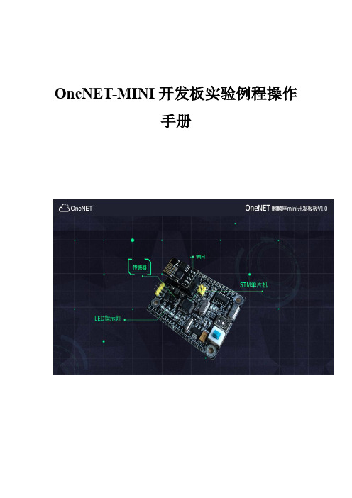
OneNET-Mini开发板实验例程操作手册 - v1.0
IE-MiniMc 用户手册说明书

Advantech B+B SmartWorx - Americas707 Dayton RoadOttawa, IL 61350 USAPhone (815) 433-5100Fax (815) 433-5105Advantech B+B SmartWorx - European HeadquartersWestlink Commercial ParkOranmore, Co. Galway, IrelandPhone +353 91-792444Fax +353 91-792445B+B SMARTWORX TECHNICAL SUPPORTUSA/Canada: 1 (800) 346-3119 (Ottawa IL USA location)(Monday - Friday, 7:00 a.m. to 7:00 p.m. CST) Europe: +353 91 792444 (Ireland location)(Monday - Friday, 8 a.m. to 5:00 p.m. GMT) Email: ************************Web: CONTENTSB+B SMARTWORX TECHNICAL SUPPORT (i)List of Figures (ii)List of Tables (iii)FCC RADIO FREQUENCY INTERFERENCE STATEMENT (iii)WARRANTY (iv)ABOUT THE IE-MINIMC (1)HARDWARE INSTALLATION -both product lines (2)hardware mounting options (2)powering options (3)LEDS (4)DC terminal block wiring instructions (5)Cascading DC Power (5)SPECIFICATIONS (6)CERTIFICATIONS/APPROVALS (7)ELECTROSTATIC DISCHARGE PRECAUTIONS (8)FIBER OPTIC CLEANING GUIDELINES (9)CERTIFICATIONS (10)LIST OF FIGURESFigure 1. Wall Mount Bracket (2)Figure 2. DIN Rail Mounting (3)LIST OF TABLESTable 1. LEDS (4)Table 2. Specifications (6)Table 3. Certifications (7)FCC RADIO FREQUENCY INTERFERENCE STATEMENTThis equipment has been tested and found to comply with the limits for a Class B computing device, pursuant to Part 15 of the FCC Rules. These limits are designed to provide reasonable protection against harmful interference when the equipment is operated in a commercial environment This equipment generates, uses and can radiate radio frequency energy and, if not installed and used in accordance with the instruction manual, may cause harmful interference to radio communications. Operation of this equipment in a residential area is likely to cause harmful interference in which the user will be required to correct the interference at his own expense.Any changes or modifications not expressly approved by the manufacturer could void the user’s authority to operate the equipment. The use of non-shielded I/O cables may not guarantee compliance with FCC RFI limits. This digital apparatus does not exceed the Class B limits for radio noise emission from digital apparatus set out in the Radio Interference Regulation of the Canadian Department of Communications. Le présent appareil numérique n’émet pas de bruits radioélectriquesdépassant les limites applicables aux appareils numériques de classe B prescrites dans le Règlement sur le brouillage radioélectrique publié par le ministère des Communications du Canada.WARRANTYEffective for products of B+B SmartWorx shipped on or after May 1, 2013, B+B SmartWorx warrants that each such product shall be free from defects in material and workmanship for its lifetime. This limited lifetime warranty is applicable solely to the original user and is not transferable.This warranty is expressly conditioned upon proper storage, installation, connection, operation and maintenance of products in accordance with their written specifications. Pursuant to the warranty, within the warranty period, B+B SmartWorx, at its option will:1. Replace the product with a functional equivalent;2. Repair the product; or3. Provide a partial refund of purchase price based on a depreciated value.Products of other manufacturers sold by B+B SmartWorx are not subject to any warranty or indemnity offered by B+B SmartWorx, but may be subject to the warranties of the other manufacturers.Notwithstanding the foregoing, under no circumstances shall B+B SmartWorx have any warranty obligations or any other liability for: (i) any defects resulting from wear and tear, accident, improper use by the buyer or use by any third party except in accordance with the written instructions or advice of the B+B SmartWorx or the manufacturer of the products, including without limitation surge and overvoltage conditions that exceed specified ratings, (ii) any products which have been adjusted, modified or repaired by any party other than B+B SmartWorx or (iii) any descriptions, illustrations, figures as to performance, drawings and particulars of weights and dimensions contained in the B+B SmartWorx’ catalogs, price lists, marketing materials or elsewhere since they are merely intended to represent a general idea of the products and do not form part of this price quote and do not constitute a warranty of any kind, whether express or implied, as to any of the B+B SmartWorx’ products.THE REPAIR OR REPLACEMENT OF THE DEFECTIVE ITEMS IN ACCORDANCE WITH THE EXPRESS WARRANTY SET FORTH ABOVE IS B+B SMARTWORX’ SOLE OBLIGATION UNDER THIS WARRANTY. THE WARRANTY CONTAINED IN THIS SECTION SHALL EXTEND TO THE ORIGINAL USER ONLY, IS IN LIEU OF ANY AND ALL OTHER WARRANTIES, EXPRESS OR IMPLIED, AND ALL SUCH WARRANTIES AND INDEMNITIES ARE EXPRESSLY DISCLAIMED, INCLUDING WITHOUT LIMITATION (I) THE IMPLIED WARRANTIES OF FITNESS FOR A PARTICULAR PURPOSE AND OF MERCHANTABILITY AND (II) ANY WARRANTY THAT THE PRODUCTS ARE DO NOT INFRINGE OR VIOLATE THE INTELLECTUAL PROPERTY RIGHTS OF ANY THIRD PARTY. IN NO EVENT SHALL B+B SMARTWORX BE LIABLE FOR LOSS OF BUSINESS, LOSS OF USE OR OF DATA INTERRUPTION OF BUSINESS, LOST PROFITS OR GOODWILL OR OTHER SPECIAL, INCIDENTAL, EXEMPLARY OR CONSEQUENTIAL DAMAGES. B&B ELECTRONIC SHALL DISREGARD AND NOT BE BOUND BY ANY REPRESENTATIONS, WARRANTIES OR INDEMNITIES MADE BY ANY OTHER PERSON, INCLUDING WITHOUT LIMITATION EMPLOYEES, DISTRIBUTORS, RESELLERS OR DEALERS OF B+B SMARTWORX WHICH ARE INCONSISTENT WITH THE WARRANTY, SET FORTH ABOVE.ABOUT THE IE-MINIMCThe IE-MiniMc Industrial Ethernet media converter features 10/100 switching copper-to-fiber conversion. Miniature in size, it offers plug-and-play operation, and supports an extended voltage range as well as extended operating temperature.. The media converter can function as a PD device, and is compliant to the IEEE 802.3af Power Over Ethernet (PoE) standard. Available in a variety of Single Mode and Multi Mode fiber types, it supports an MTU of 1916 bytes. Several mounting options and powering options are available and detailed in the following sections of the manual.HARDWARE INSTALLATION -BOTH PRODUCT LINES The IE-MiniMc installs virtually anywhere as a standalone device in locations with extremely limited space. Installation options include:·Velcro strips·DIN rail mounting with DIN Rail clips· A wall mount bracket· A PowerTray/18 for high density applicationsHARDWARE MOUNTING OPTIONSThe IE-MiniMc can be mounted on a DIN rail or using wall mount brackets (shown below).Figure 1. Wall Mount BracketDIN rail clips (part number 806-39105) and wall mount brackets (part number 895-39229) are available for purchase through an B&B Electronics Distributor. The DIN Rail clips include screws, to allow the installation onto a DIN Rail. Install the screws into DIN Rail clips, which should be mounted parallel or perpendicular to the DIN Rail. Snap the converter onto the clips. To remove the converter from the DIN Rail, use a flat-head screwdriver into the slot to gently pry the converter from the rail.Figure 2. DIN Rail MountingPOWERING OPTIONSThe IE-MiniMc includes multiple powering options:· A country-specific, high-reliability AC power adapter (included)·The IEEE 802.3af Power over Ethernet standard; draws power from power sourcing equipment (NON-Telco version only)·The 4-terminal DC power block·IE-PowerTray/18 for Rack MountingPower Over EthernetPower Over Ethernet technology allows the IE-MiniMc to be a Powered Draw device (PD) and draw power when connected to Power Sourcing Equipment (PSE). Power Sourcing Equipment distributes an electrical current across existing copper data cabling.LEDSEach IE-MiniMc includes two LEDs, located on the RJ-45 connector.LED functions are as follows:FXLNK/ACT Glows green when a link is established on the fiber port; blinks green when activity is detected on the fiber port.TXLNK/ACT Glows amber when a link is established on the copper port; blinks amber when activity is detected on the copper port.Table 1. LEDSDC TERMINAL BLOCK WIRING INSTRUCTIONSThe IE-MiniMc can also be powered with the DC terminal block. From a power source, connect to any one positive and any one negative terminal on the IE-MiniMcFigure 3. DC Terminal BlockNOTEWhen using stranded wire, the leads must be tinned and equivalent to a 16 AWG solid conductor. The DC terminal block is protected against mis-wiring. If the unit is mis-wired, positive power lead to the negative terminal and negative power lead to the positive terminal, it will not function. When powering a unit with voltages near the upper limit of the device’s specification (for example: 50 volts) take precautions to limit the voltage at the units terminal block. When turning on high voltage DC circuits, initial voltages may exceed the maximum allowed duration of the unit’s transient protection devices.Cascading DC PowerWhen installing multiple IE-MiniMc units on a DIN rail, the end user can connect to one DC input source, and then cascade from one DC block to the next, until reaching the maximum current available.SPECIFICATIONSConnectorsCopper RJ-45Fiber ST, SCEnvironmental -- Intended for indoor and outdoor use.Operating Temperature -40°F to +185°F (-40°C to +85°C) DC configuration +14°F to +122°F (-10°C to +50°C) with AC wall adapterStorage Temperature-40°F to +185°F (-40°C to +85°C)Operating Humidity 5 to 95% (non-condensing); 0 to 10,000 ft. altitude LED Indicators One Green LEDCopper RJ-45 port LNK/ACT Color = GREENBlink = GREEN when data is passing Off = NO COLORFiber Port LNK/ACT Color = AMBERBlink = AMBER when data is passing Off = NO COLORPower InputDC Terminal Block 7 to 50 VDC, 1-0.1ADC jack 5 to 24 VDCPoE When IE-MiniMc uses PoE technology to be a PD,the maximum supply voltage is 50VTable 2. SpecificationsCERTIFICATIONS/APPROVALSCertificationsFCC FCC Part 15 Class BCEEN55022 CISPR 22 Class BEN61000-3-2 Generic Standards for Residential, Commercial, & Light IndustrialEN61000-4-2 ESD (15kV air & 4kV contact)EN61000-4-3 RFIEN61000-4-4 EFTEN61000-4-5 SurgeEN61000-4-6 CIEN61000-4-8 Power Frequency MagneticVoltage Dips & InterruptionsEN61000-4-11Regulatory ApprovalsROHS and WEEE CompliantTable 3. CertificationsELECTROSTATIC DISCHARGE PRECAUTIONS Electrostatic discharge (ESD) can cause damage to any product, add-in modules or stand-alone units, containing electronic components. Always observe the following precautions when installing or handling these kinds of products:Do not remove unit from its protective packaging until ready to install. Wear an ESD wrist grounding strap before handling any module or component. If the wrist strap is not available, maintain grounded contact with the system unit throughout any procedure requiring ESD protection. Hold the units by the edges; do not touch the electronic components or gold connectors.After removal, always place the boards on a grounded, static-free surface, ESD pad or in a proper ESD bag. Do not slide the modules orstand-alone units over any surface. WARNING! Integrated circuits and fiber optic components are extremely susceptible to electrostatic dischargedamage. Do not handle these components directly unless you are a qualified service technician and use tools andtechniques that conform to accepted industry practices.FIBER OPTIC CLEANING GUIDELINESFiber optic transmitters and receivers are extremely susceptible to contamination by particles of dirt or dust, which can obstruct the optic path and cause performance degradation. Good system performance requires clean optics and connector ferrules.Use fiber patch cords (or connectors, if you terminate your own fiber) only from a reputable supplier; low-quality components can cause many hard-to-diagnose problems in an installation.Dust caps are installed at B+B SmartWorx to ensure factory-clean optical devices. These protective caps should not be removed until the moment of connecting the fiber cable to the device. Should it be necessary to disconnect the fiber device, reinstall the protective dust caps.Store spare caps in a dust-free environment such as a sealed plastic bag or box so that when reinstalled they do not introduce any contamination to the optics.If you suspect that the optics have been contaminated, alternate between blasting with clean, dry, compressed air and flushing with methanol to remove particles of dirt.CERTIFICATIONSCE: The products described herein comply with the Council Directive on Electromagnetic Compatibility (2004/108/EC). For further details, contact B+B SmartWorx.European Directive 2002/96/EC (WEEE) requires that any equipment that bears this symbol on product or packaging must not be disposed of with unsorted municipal waste. This symbol indicates that the equipment should be disposed of separately from regular household waste. It is the consumer’s responsibility to dispose of this and all equipment so marked through designated collection facilities appointed by government or local authorities. Following these steps through proper disposal and recycling will help prevent potential negative consequences to the environment and human health. For more detailed information about proper disposal, please contact local authorities, waste disposal services, or the point of purchase for this equipment.____________________________________________________© 2017 B+B SmartWorx. All rights reserved. The information in this document is subject to change without notice. B+B SmartWorx assumes no responsibility for any errors that may appear in this document. IE-MiniMc is a trademark of B+BSmartWorx. Other brands or product names may be trademarks and are the property of their respective companies.Document #: 55-80722-00-A8_1017。
MINI-V3助学版用户手册
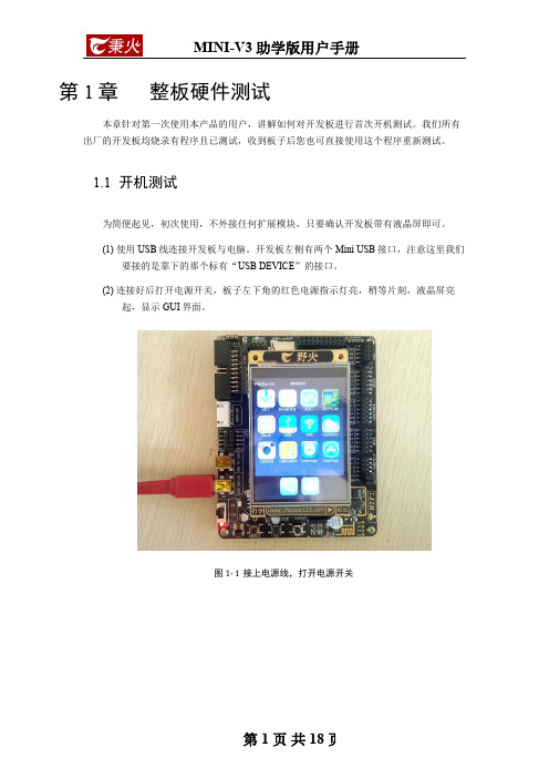
第1章整板硬件测试本章针对第一次使用本产品的用户,讲解如何对开发板进行首次开机测试。
我们所有出厂的开发板均烧录有程序且已测试,收到板子后您也可直接使用这个程序重新测试。
1.1开机测试为简便起见,初次使用,不外接任何扩展模块,只要确认开发板带有液晶屏即可。
(1)使用USB线连接开发板与电脑。
开发板左侧有两个Mini USB接口,注意这里我们要接的是靠下的那个标有“USB DEVICE”的接口。
(2)连接好后打开电源开关,板子左下角的红色电源指示灯亮,稍等片刻,液晶屏亮起,显示GUI界面。
图1-1接上电源线,打开电源开关图1-2开机后的液晶界面截图进入主界面后,说明开发板功能正常,您可随意尝试打开各个APP,自行把玩。
当然,有很多APP是需要扩展硬件模块才可以正常使用的,所以打开后提示错误请放心,并不是开发板的问题,只是板子没有连接支持该APP的硬件模块。
可能遇到的简单故障排查:(1)打开开关后电源灯不亮。
❑检查USB线连接。
❑重复多次打开电源开关。
❑更换USB线。
❑把USB线接到另一个标有“USB TO UART”的接口。
(2)电源灯亮,液晶屏无现象或显示的不是以上截图的界面。
❑可能是液晶屏接触不良,把液晶屏拆下来,重新接上。
❑确认没有自行给开发板下载过其它程序,若下载过其它程序,请重新给开发板下载配套资料里的出厂测试程序。
❑使用万用表检查USB线供电的电压,在4.2-5.5V范围可认为电压正常。
若遇到问题无法解决,请联系我们。
1.2APP使用说明在主界面下,点击APP的图标即可运行,而在APP界面下触摸开发板的“电容按键”可返回主界面,同时蜂鸣器会响一下,也可直接点击APP右上方的“x”返回主界面。
下面对各个APP的使用方式进行说明。
1.KEY图1-3KEY APP界面运行KEY APP可使用板子上的按键控制LED灯。
进入APP界面后,按下开发板上的KEY1和KEY2按键可控制LED的亮灭。
也可点击界面上的两个“KEY”按钮,按钮按下时,会有对应的LED灯被点亮。
Mini ToolStick用户手册(V1.0)

Mini ToolStick For C8051F MCU用户手册目录Mini ToolStick简介 (1)开发工具特点 (1)产品标配附件 (1)调试器接口关系图 (2)Mini ToolStick安装说明 (3)Mini ToolStick在Silabs IDE中的设置说明 (4)Mini ToolStick在Keil3中的设置说明 (9)Mini ToolStick在IAR中的设置说明 (13)Mini ToolStick常见问题解决方法 (15)用户手册版本历史 (15)Mini ToolStick简介:C8051F单片机的低价位开发套件是为您提供快速开发应用系统的工具。
该套件包含了开发所需的软件和硬件,性能优于传统的调试器。
Mini ToolStick具有:完全的USB2.0接口、免安装驱动程序、硬件加强型保护功能(减少使用不当造成的硬件损坏率)。
该工具可实现单步、连续单步、断点、停止/运行,支持寄存器/存储器的观察和修改,下载程序到Flash存储器等功能。
本开发工具有如下特点:1、全速率USB2.0接口,硬件加强型保护功能(减少使用不当造成的硬件损坏率)。
2、Mini ToolStick在第①脚提供3.3V250mA的稳压电源,可向目标板直接供电。
3、兼容国内外所有C8051F单片机调试器,所有软件也同样适用本开发系统。
4、调试电路采用专用电平转换芯片,支持C8051F全系列(C2和JTAG接口)MCU。
5、自动固件升级,使本产品支持Silabs公司未来生产的C8051F MCU系列产品。
6、本开发工具为普通U盘大小,可直接插在电脑上使用,非常便于外出携带。
7、Windows Me以上系统不需要驱动,直接使用。
8、本产品可与IAR Embedded Workbench for MCS-51、KeilμVsion2/3、SiliconLaboratories IDE软件无缝连接调试。
物联网实训仿真系统用户使用手册2018-7-6

物联网云-仿真实训台用户使用手册文档文档历史/修订记录目录1 功能概述 (5)2运行环境 (5)2.1硬件环境 (5)2.2软件环境 (5)3界面介绍 (6)3.1主界面 (6)3.1.1结构图 (6)3.1.2工具栏 (6)3.1.3 设备区 (7)3.2设计区 (7)3.2.1结构图 (7)3.2.2工具栏 (8)3.2.3比例尺 (10)3.2.4 标签页栏 (10)3.3下拉菜单 (10)3.4 设置界面 (11)3.4.1配置项 (11)4设备介绍 (11)4.1供电状态 (12)4.1供电类型 (12)4.2连线状态 (12)5功能介绍 (13)5.1设备操作 (13)5.1.1设备拖放 (13)5.1.2设备拖动 (13)5.1.3设备编辑 (14)5.1.4设备多选 (14)5.1.5设备对齐 (15)5.1.5设备排序 (15)5.2工作台操作 (15)5.2.1新建工作台 (15)5.2.2重命名工作台 (15)5.2.3关闭工作台 (15)5.2.4标签栏调整 (16)5.2.5缩放比例调整 (16)5.2.6视角快速切换 (16)5.3连线操作 (16)5.3.1新建连线 (16)5.3.2连线编辑 (17)5.3.3连线验证 (17)5.4仿真包操作 (18)5.4.1仿真包保存 (18)5.4.3仿真包打开 (19)5.5虚拟仿真 (19)5.5.1设备属性 (19)5.5.2模拟数据 (19)5.5.3 配置虚拟COM口 (20)5.5.4配置虚拟USB口 (22)5.6获取传感器数据 (23)1 功能概述2运行环境2.1硬件环境a.处理器:1GHzb.RAM:512MBc.磁盘空间:32位:4.5GB64位:4.5GB2.2软件环境a.操作系统:Windows 7/8/10b..NET Framework 4.53界面介绍3.1主界面3.1.1结构图①: 工具栏②: 设备区③: 设计区3.1.2工具栏a.创建:新建新的工作台b.打开:从仿真包文件新建工作台c.保存:保存当前更改到仿真包d.另存为:另存为新的仿真包e.全部保存:保存工作台中所有打开的仿真包f.撤销:撤销本次操作g.恢复:恢复上一步操作h.排序:顶端对齐、上下居中、低端对齐、左对齐、左右居中、右对齐;上移一层、下移一层、移至顶层、移至底层3.1.3 设备区截图:树形结构:3.2设计区3.2.1结构图①:设计区工具栏②:工作面板③:比例尺④:标签栏3.2.2工具栏a.连线验证:对当前工作台中的连线进行验证,默认为关闭状态,开启后,会实时的对连线进行验证。
Mininet日常使用一(官网)
Mininet⽇常使⽤⼀(官⽹)第1部分:⽇常Mininet使⽤⾸先,此演练的命令语法(可能很明显):$先于应在shell提⽰符下键⼊的Linux命令mininet>先于应在Mininet的CLI上键⼊的Mininet命令,#先于在root shell提⽰符下键⼊的Linux命令在每种情况下,您只应在提⽰符右侧键⼊命令(然后按return,当然!)。
显⽰启动选项让我们开始使⽤Mininet的启动选项。
键⼊以下命令以显⽰描述Mininet的启动选项的帮助消息:$ sudo mn -h本演练将涵盖列出的⼤多数选项的典型⽤法。
启动Wireshark要使⽤OpenFlow Wireshark解剖器查看控制流量,请⾸先在后台打开Wireshark:$ sudo wireshark &在“ Wireshark”过滤器框中,输⼊此过滤器,然后单击Apply:of在Wireshark中,单击“捕获”,然后单击“接⼝”,然后在回送接⼝(lo)上选择“启动” 。
⽬前,主窗⼝中不应显⽰任何OpenFlow数据包。
注意:默认情况下,Wireshark安装在Mininet VM映像中。
如果您使⽤的系统没有安装Wireshark和OpenFlow插件,则可以使⽤Mininet的install.sh脚本安装这两个系统,如下所⽰:1.$ cd ~2.$ git clone https:///mininet/mininet # if it's not already there3.$ mininet/util/install.sh -w如果已安装Wireshark,但您⽆法运⾏它(例如,出现诸如的错误$DISPLAY not set,请查阅FAQ: : 。
)正确设置X11将使您能够运⾏其他GUI程序和xterm终端仿真器,这些功能将在本演练的稍后部分中使⽤。
与主机和交换机交互启动最⼩拓扑并输⼊CLI:$ sudo mn默认拓扑是minimal拓扑,它包括⼀个连接到两台主机的OpenFlow内核交换机,以及OpenFlow参考控制器。
串口屏MINIC教程6-for循环和数组使用说明V1.0

(2) 打开 VisualTFT,在软件右下角可以查看软件版本图 2- 2 所示,最新版本可登录 大彩官网下载。
图 2- 2 软件版本
2. 串口屏固件版本: 基本型(经济型、商业型): MB 2.22.912.259 及以上的版本支持; 物联型:V3.0.301.0 及以上的版本支持; F 型:V4.1.66.0 及以上的版本支持。
图 3- 3 变量类型表
局部变量的定义方法如图 3- 4 所示;
图 3- 4 局部变量定义 4/ 18
MINIC 教程-for 循环和数组使用说明 V1.0
3.3 API 函数说明
本教程文档中所涉及到的部分的相关接口函数
1. 函数 void on_init() 功能:系统执行初始化,加载工程的时候执行一次。
5. 完整程序清单.................................................................................................16 6. 免责声明.........................................................................................................18
MINIC 教程-for 循环和数组使用说明 V1.0
1. 适合范围
文档适合广州大彩基本型、经济型、商业型、F 型、物联型、86 盒、485 系列等所有 MODBUS 协议的串口屏产品。
1/ 18
MINIC 教程-for 循环和数组使用说明 V1.0
2. 开发环境版本
1. VisualTFT 软件版本:V3.0.0.827 及以上的版本,版本查看方式: (1) 打开 VisualTFT 软件启动页面如图 2- 1 所示,右上角显示的软件版本号;
NVIDIA Jetson AGX Orin 开发板使用指南说明书

Steps for Flashing Jetson OrinContentsPurpose (3)Tools & Supplies (3)Flashing the Jetson (5)Confirming Jetpack is Successfully Installed on the Jetson (15)Downloading & Installing Cross Compilation Tools (15)Setting Up Environment Variables (15)Downloading Kernel on the Host (16)Modifying and Building Kernel on the Host (17)Flashing Newly Modified Kernel on to the Jetson (19)Complications Faced (20)Table of FiguresFigure 1 - Jetson AGX Orin Dev Kit (3)Figure 2 - Jetson Power Supply (3)Figure 3 - USB Type A to Type C Cable (4)Figure 4 - USB Type A to Micro USB Type-B Cable (4)Figure 5 - Display Port Cable (4)Figure 6 - Connecting Micro USB Type-B Cable to Jetson Micro USB Type-B Port (5)Figure 7 - Connecting USB Type-C to Jetson for Flashing (5)Figure 8 - Recovery & Restart Buttons (6)Figure 9 - SDKManager Icon (6)Figure 10 - SDK Manager (Step 1 Screen) (7)Figure 11 - CONTINUE TO STEP 02 (8)Figure 12 - STEP 02 Configurations Selected (9)Figure 13 - Accepting Terms & Conditions (9)Figure 14 - CONTINUE TO STEP 03 (10)Figure 15 - Create Folders (10)Figure 16 - Enter Password (11)Figure 17 - Verifying System Readiness to Install (11)Figure 18 - Jetson Configurations (prior to making modifications) (12)Figure 19 - Jetson Configurations (after making modifications) (13)Figure 20 - Flash the Jetson (14)Figure 21 - Accepting to Continue Installing Package (14)Figure 22 - STEP 04 SUMMARY FINALIZATION (14)Figure 23 - Finish Installation (15)Figure 24 - Recovery & Restart Buttons (19)PurposeThe purpose of this document is to outline the steps performed for flashing the Jetson Orin as well as modifying and loading a new kernel on the Jetson.Tools & SuppliesThis section lists the hardware and software tools used.•Host Desktop:o Operating System: Ubuntu•Jetson AGX Orin Developer Kit (figure obtained from online) [Figure 1]Figure 1 - Jetson AGX Orin Dev Kit•Jetson Power Supply [Figure 2]o Also need a power adaptor cable to plug into an outlet but that is not pictured in the image belowFigure 2 - Jetson Power Supply•USB Type-A 2.0 to USB Type-C cable (figure obtained from online) [Figure 3]Figure 3 - USB Type A to Type C Cable•USB Type-A 2.0 to Micro USB Type-B cable (figure obtained from online) [Figure 4]Figure 4 - USB Type A to Micro USB Type-B Cable•Display Port Cable (for the Jetson) (figure obtained from online) [Figure 5]Figure 5 - Display Port Cable•Two USB Mouse & Keyboard (one for the Jetson & one for the Host desktop) •Display Cable (for the Host desktop)•Two RJ45 cableo One to connect Host desktop to the networko Second to connect Jetson to the Host desktopFlashing the JetsonThis section outlines the steps performed to flash the Jetson.1.Connected the Micro USB Type-B end of the cable to the Micro USB port on the Jetson [Figure 6]Figure 6 - Connecting Micro USB Type-B Cable to Jetson Micro USB Type-B Port2.Connected the other end of the Micro USB cable (USB Type-A 2.0) to the Host desktop’s USBport3.Connected the USB Type-C cable to the Jetson’s USB Type-C port (designated for flashing)[Figure 7]Figure 7 - Connecting USB Type-C to Jetson for Flashing4.Connected the other end of the USB Type-C cable to the Host desktop’s USB port5.Connected an RJ45 cable to the Jetson and connected the other end to the Host desktop6.Connected the Jetson to its power supply and connected the power supply to a plug outlet7.The next set of steps (steps 8 to 34) were performed on the Host desktop8.Note: Since previously these steps have been performed, the following steps were done first:a.Removed the ~/nvidia folder by entering the command below in the terminalb.Removed the ~/Downloads/nvidia folder by entering the command below in theterminalc.Removed the NVIDIA SDKManager’s databas e file by entering the command below inthe terminal9.Put the Jetson in recovery mode by pushing the “recovery” button then pushing the “restart”button and releasing both at the same time [Figure 8]Figure 8 - Recovery & Restart Buttons10.Entered the command below on the terminal on the Host desktop to confirm the Jetson is inrecovery mode, which it was:a.NOTE: “NVIDIA” device is found, so the Jetson is in recovery mode11.Opened the SDKManager application by finding the application and clicking on it [Figure 9]Figure 9 - SDKManager Icon12.When opened, a login prompt was seen13.Logged in with my username (email) and password14.Then the following window was seen, and selected the following configurations [Figure 10]a.Product Category : Selected Jetsonb.Hardware Configuration : Disabled itc.Target Hardware : Enabled and selected JetsonAGX Orind.Target Operating System : Linux JetPack 5.0.2 (rev. 1)e.Additional SDKS: Disabled DeepStream 6.1.1Figure 10 - SDK Manager (Step 1 Screen)15.Next clicked “CONTINUE TO STEP 02” (circled in the image below) [Figure 11]Figure 11 - CONTINUE TO STEP 0216.In “STEP 02 DETAILS AND LICENSE” page, the “Jetson SDK Components” was disabled while the“Jetson Linux” was enabled as shown below [Figure 12]Figure 12 - STEP 02 Configurations Selected17.Then selected “I accept the terms and conditions of the license agreements” checkbox on thebottom of the screen (circled in the image below) [Figure 13]Figure 13 - Accepting Terms & Conditions18.Then clicked on the “CONTINUE TO STEP 03” button (circled in the image below) [Figure 14]Figure 14 - CONTINUE TO STEP 0319.The following pop up seen, selected “Create” (circled in the image below) [Figure 15]Figure 15 - Create Folders20.Then another popup was displayed requesting for administrative password, entered thepassword then clicked “OK” (circled in the image below) [Figure 16]f.NOTE: The “OK” button turns to light green after entering password in the textboxFigure 16 - Enter Password21.Then a popup is displayed that wrote “SDK Manager is verifying system readiness to install”[Figure 17]Figure 17 - Verifying System Readiness to Install22.After a few minutes, the popup disappeared and progress bars were displayed on theSDKManager’s window on the bottom of the page where the folder paths were23.Waited for a few minutes (could take about 20-30 depending on host configurations)24.After a few minutes, the following window was seen stating the SDK Manager is ready to flashthe Jetson AGX Orin module [Figure 18]Figure 18 - Jetson Configurations (prior to making modifications)25.For the setup mode, selected “Manual Setup –Jetson AGX Orin”26.For the “OEM Configuration”, selected “Pre-Config”27.Entered username and password28.For the “Storage Device”, selected “EMMC (default)”29.Below is an image of the settings selected listed in steps 25 to 28 [Figure 19]Figure 19 - Jetson Configurations (after making modifications)30.Once confirmed proper configurations are selected, clicked on “Flash” (circled in the imagebelow) [Figure 20]Figure 20 - Flash the Jetson31.NOTE: If a popup is seen stating installation is taking longer than expected, select “Yes” (circledin the image below) [Figure 21]Figure 21 - Accepting to Continue Installing Package32.After a while, the “STEP04 SUMMARY FINALIZATION” is reached and it stated the installationcompleted successfully [Figure 22]Figure 22 - STEP 04 SUMMARY FINALIZATION33.Then selected “FINISH AND EXIT” (circled in the image below) [Figure 23]Figure 23 - Finish InstallationConfirming Jetpack is Successfully Installed on the JetsonOn the Jetson, it was confirmed the Jetpack was installed and were able to successfully boot it up and log in to it.Downloading & Installing Cross Compilation ToolsFollowed the instructions in the link below to download, install, and set up the cross compilation tools on the Host desktop:https:///jetson/archives/r34.1/DeveloperGuide/text/AT/JetsonLinuxToolchain.html Setting Up Environment VariablesThe following steps were performed on the Host desktop to set up the environment variables to be used in the proceeding sections:1.Entered the commands below on the terminal to set up environment variables:Downloading Kernel on the HostThe following steps were performed on the Host desktop to download the kernel:1.Entered the command below on the terminal to change directory to the JetPack folder:~/nvidia/nvidia_sdk/JetPack_5.0.2_Linux_Jetson_AGX_ORIN_TARGETS/Linux_for_Tegra/2.Entered the command below on the terminal to create a folder named “sources” and tochange directories to it:~/nvidia/nvidia_sdk/JetPack_5.0.2_Linux_Jetson_AGX_ORIN_TARGETS/Linux_for_Tegra/sources/3.Entered the command below on the terminal to download the sources from NVIDIA:4. Entered the command below on the terminal to extract the contents from thepublic_sources.tbz2 file:5.Entered the command below on the terminal to extract the contents from thekernel_src.tbz2 file:Modifying and Building Kernel on the HostThe following steps were performed on the Host desktop to modify and build the kernel:1.Entered the command below on the terminal to create the ${KERNEL_MODULES_OUT}folder:2.Entered the command below on the terminal to change directory to the kernel folder:~/nvidia/nvidia_sdk/JetPack_5.0.2_Linux_Jetson_AGX_ORIN_TARGETS/Linux_for_Tegra/sources/kernel/ke rnel-5.03.NOTE: Some websites like the one belowhttps:///wiki/index.php/NVIDIA_Jetson_Orin/JetPack_5.0.2/Compiling_ Code/Kernelspecify to make some changes to fix some errors in the kernel. However, that was not needed for this kernel that was downloaded4. Next, the tegra_defconfig file is modified to include “CONFIG_SENSOR_LTC2990=y”in it by entering the command below to open the filea.NOTES:i.Any text editor of choice could be used here, “vi” was used in this caseii.Instructions on how to use “vi” to modify a file and save/close it is beyond the scope of this document5.Entered the command below on the terminal to create the .config file:a.NOTE: The log file could be found in the Jetson_Logs_20221026.zip file (log file name issetup_dflt_cnfg.log)6.Entered the command below on the terminal to create the BSP:bsp.log)7.Entered the command below on the terminal to install the modules:a.NOTE: The log file could be found in the Jetson_Logs_20221026.zip file (log file name ismodules_install.log)8.Entered the commands below on the terminal to create backups of existing files:9.Entered command below on the terminal to change directory to the ${KERNEL_OUT}folder:~/nvidia/nvidia_sdk/JetPack_5.0.2_Linux_Jetson_AGX_ORIN_TARGETS/Linux_for_Tegra/images/10.Entered the commands below on the terminal to copy newly created files to the designatedlocations:11.Entered the command below on the terminal to change directory to the${KERNEL_MODULES_OUT} folder:~/nvidia/nvidia_sdk/JetPack_5.0.2_Linux_Jetson_AGX_ORIN_TARGETS/Linux_for_Tegra/images/modules12.Entered the command below to compress the kernel modules folder:13.Entered the command below to apply the binaries:a.NOTE: The log file could be found in the Jetson_Logs_20221026.zip file (log file name isapply_binaries.log)Flashing Newly Modified Kernel on to the JetsonThe following steps were performed on the Host desktop to flash the newly modified kernel on the Jetson:1.Entered the command below to change directory to the location where the flash.sh script islocated:a.Current folder right now is:~/nvidia/nvidia_sdk/JetPack_5.0.2_Linux_Jetson_AGX_ORIN_TARGETS/2.Entered the command below on the terminal to check if the Jetson is in a recovery mode or not,and confirmed it wasn’t:a.NOTE: No “NVIDIA” device is found, so the Jetson is not in reco very mode3.Pushed the “recovery” button, then pushed the “restart” button and released both at the sametime to place the Jetson in recovery modeFigure 24 - Recovery & Restart Buttons4.Entered the command below on the terminal to confirm the Jetson is in recovery mode which itwas:a.NOTE: “NVIDIA” device is found, so the Jetson is in recovery mode5.Entered the command below on the terminal to flash the kernel on the Jetson:a.Complications FacedOnce the kernel completed loading, the following steps were performed:1.On the Host desktop, opened a terminal window and opened minicom by entering thecommand below:2.When in minicom, hit the enter key on the keyboard a few times which then displayed Linuxinstallation setup prompts3.Went through the setup prompts (selecting time zone, language, etc.)4.Once completed, it attempted to boot up but stopped at the following lines in the boot upmessages (seen from the serial console on minicom):a.NOTE: The log file could be found in the Jetson_Logs_20221026.zip file (log file name isBoot_Up.log)i.NOTE: Noticed a kernel panic occur in this log5.Power cycled the unit, it attempted to boot up and still stopped at the following lines:a.NOTE: NVIDIA Splash screen was displayed on the monitor, but after that, the monitorwent blank6.Attempted Step 5 with the following modifications, but still witnessed same issue:a.Connected the Jetson to the networkb.Disconnected RJ45 cable from the Jetsoni.NOTE: The log file when no RJ45 cable is connected could be found in theJetson_Logs_20221026.zip file (log file name is Second_Attempt_Boot_Up.log)21。
Mini51用户指导手册

奋斗版STM32开发板Mini板硬件说明书NEW
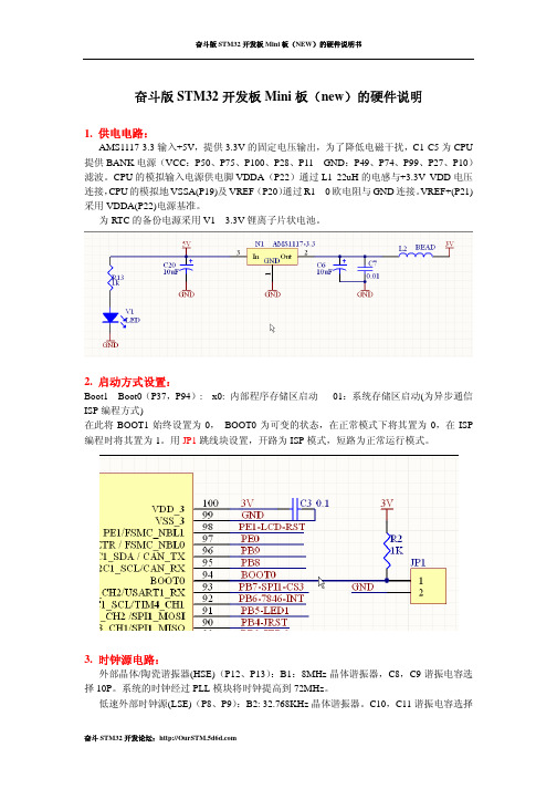
奋斗版STM32开发板Mini板(new)的硬件说明1. 供电电路:AMS1117-3.3输入+5V,提供3.3V的固定电压输出,为了降低电磁干扰,C1-C5为CPU 提供BANK电源(VCC:P50、P75、P100、P28、P11 GND:P49、P74、P99、P27、P10)滤波。
CPU的模拟输入电源供电脚VDDA(P22)通过L1 22uH的电感与+3.3V VDD电压连接,CPU的模拟地VSSA(P19)及VREF-(P20)通过R1 0欧电阻与GND连接。
VREF+(P21)采用VDDA(P22)电源基准。
为RTC的备份电源采用V1 3.3V锂离子片状电池。
2. 启动方式设置:Boot1—Boot0(P37,P94): x0: 内部程序存储区启动01:系统存储区启动(为异步通信ISP编程方式)在此将BOOT1始终设置为0, BOOT0为可变的状态,在正常模式下将其置为0,在ISP 编程时将其置为1。
用JP1跳线块设置,开路为ISP模式,短路为正常运行模式。
3. 时钟源电路:外部晶体/陶瓷谐振器(HSE)(P12、P13):B1:8MHz晶体谐振器,C8,C9谐振电容选择10P。
系统的时钟经过PLL模块将时钟提高到72MHz。
低速外部时钟源(LSE)(P8、P9):B2: 32.768KHz晶体谐振器。
C10,C11谐振电容选择10P。
注意:根据ST公司的推荐, B2要采用电容负载为6P的晶振,否则有可能会出现停振的现象。
4. SPI存储电路:D2 AT45DB161(2M Bytes)CPU采用SPI1端口PA7-SPI1-MOSI(P32)、PA6-SPI1-MISO (P31)、PA5-SPI1-SCK(P30)、PA4-SPI1-NSS(P29)控制读写访问, SPI1地址:0x4000 3800 - 0x4000 3BFF5. 显示及触摸接口模块:显示器采用2.4” TFT320X240LCD(控制器ILI9325), 采用CPU的FSMC功能,LCD片选CS采用FSMC_NE1(P88),FSMC_A16(P58)作为LCD的RS选择,FSMC_nWE(P86)作为LCD的/WR, FSMC_nOE(P85)作为LCD的/RD, LCD的RESET脚用CPU的PE1(P98)(LCD-RST),FSMC_D0---FSMC_D15和LCD的D1-D8 D10-D17相互连接,触摸屏接口采用SPI1接口,片选为PB7-SPI1-CS3,由于LCD背光采用恒流源芯片PT4101控制,采用了PWM控制信号控制背光的明暗, PWM信号由PD13-LIGHT-PWM来控制。
龙芯1C嵌入式开发板手册说明书

智龙开发板手册——基于龙芯1C的嵌入式开发板版本历史版本日期备注V1.02015-05-30基于智龙V1.0,创建手册V2.02015-10-21结合智龙开发者的经验和龙芯官方1C300B开发板手册编写目录1硬件篇 (7)1.1龙芯1C芯片介绍 (8)1.2智龙开发板介绍 (9)1.3智龙开发板硬件接口 (13)SDRAM控制器 (15)SRAM/NOR FLASH控制器 (15)NAND控制器 (15)时钟发生器 (18)I2S控制器 (19)AC97控制器 (19)LCD控制器 (19)Camera接口 (19)MAC控制器 (19)USB2.0控制器 (20)SPI控制器 (20)I2C控制器 (20)UART控制器 (20)GPIO (21)PWM控制器 (21)RTC (21)CAN控制器 (22)SDIO控制器 (22)ADC控制器 (22)1.4串口调试连接 (22)1.5eJtag调试系统 (27)1.6Flash烧写PMON引导系统 (28)1.7Flash烧写linux系统(附带跑马灯实验) (32)2软件篇 (42)2.2Linux内核裁剪和配置 (44)2.2.1安装图形化配置工具Ncurses (44)2.2.2运行图形化配置界面 (45)2.2.3编译Linux内核 (46)2.2.4开发板各模块驱动源码 (46)2.3配置内核各模块驱动 (48)2.3.1配置网卡驱动 (48)2.3.2配置NFS支持 (51)2.3.3配置UBIFS支持 (54)2.3.4配置串口驱动 (57)2.3.5配置LCD驱动 (59)2.3.6配置按键驱动 (61)2.3.7配置SD卡驱动 (63)2.3.8配置U盘驱动 (65)2.3.9配置USB鼠标和键盘驱动 (68)2.3.10配置USB OTG驱动 (72)2.3.11配置音频驱动 (74)2.3.12配置RTC驱动 (76)2.3.13配置PWM驱动 (78)2.3.14配置红外驱动 (81)2.3.15配置CAN总线驱动 (82)2.3.16配置SPI控制器驱动 (85)2.3.17配置I2C控制器驱动 (87)2.3.18配置ADC驱动 (89)2.3.19配置GPIO驱动 (90)2.3.20配置看门狗驱动 (92)2.3.21配置中星微zc301USB摄像头驱动 (93)2.4Linux、PMON、Rootfs镜像制作 (96)2.5Linux系统的交叉编译环境的搭建 (99)2.5.2新建Ubuntu虚拟机 (101)2.5.3安装Ubuntu系统 (109)2.5.4备份恢复Ubuntu虚拟机 (119)2.6使用Ubuntu12.04 (122)2.6.1Ubuntu终端 (122)2.6.2设置Ubuntu虚拟机网络 (124)2.6.3安装VMware Tools (129)2.6.4更新Ubuntu软件包列表 (131)2.6.5设置Windows和Ubuntu的共享文件夹 (131)2.6.6安装配置minicom串口工具 (133)2.6.7安装配置TFTP服务器 (142)2.6.8安装配置NFS服务器 (146)2.6.9建立交叉编译环境 (149)2.7PMON的配置和编译 (150)2.7.1安装依赖库和编译工具 (150)1连网在线安装 (150)2使用源码包安装 (150)2.7.2配置PMON (152)1配置系统启动方式 (152)2配置串口 (152)2.7.3编译PMON (153)2.8基于linux的根文件系统 (153)2.8.1创建文件系统目录 (153)2.8.2创建系统配置文件 (153)2.8.3拷贝库文件 (156)2.9制作根文件系统镜像 (157)2.9.1安装镜像文件制作工具 (157)2.9.2制作根文件系统镜像文件 (160)2.10基于linux的网络配置 (161)2.11基于linux的交叉编译Helloworld (164)2.12基于linux的Python移植 (170)2.13基于linux的PWM控制LED (171)2.14RT-Thread实时系统移植 (177)2.14基于RTT编写PWM驱动 (177)2.15基于RTT的LED和按键的控制 (177)3应用篇 (177)3.1龙芯wifi小车 (177)3.2英国智龙摩尔电码播放器 (178)3.3俄罗斯方块 (195)3.4智龙连接物联网平台智城云 (200)3.5智龙连接微信公众号 (200)3.63D打印机主板 (200)附录 (200)龙芯1C引脚复用表 (200)Linux常用命令 (200)PMON命令 (200)1硬件篇主要介绍龙芯1C芯片以及智龙开发板相关硬件设计图龙芯1C300A图智龙V2.0开发板1.1龙芯1C芯片介绍龙芯1C300(以下简称1C)芯片是基于LS232处理器核的高性价比单芯片系统,可应用于指纹生物识别、物联传感等领域。
PoC手册 - 1 基础环境 - Lab 07 NetScaler基本安装及配置1.0

标准化实施方案| 白皮书| Citrix XenDesktop/XenApp/NetScalerPoC标准化实施指南基础环境07 NetScaler基本安装及配置版本:v1.0目录修正历史 (2)第1章基本过程 (3)1.1 安装配置环境 (4)第2章基础环境准备——DNS解析配置 (5)第3章StoreFront结合NetScaler配置 (10)第4章NetScaler配置 (16)4.1 NetScaler VPX虚拟机导入 (16)4.2 NetScaler基础配置 (23)4.3 NetScaler服务器证书申请及安装 (28)4.3.1 NetScaler服务器证书申请 (28)4.3.2 NetScaler服务器证书安装 (37)4.4 NetScaler Gateway配置向导 (39)4.5 使用IOS设备第一次登录失败 (44)4.6 访问验证及NetScaler Gateway登录首页风格优化 (46)4.7 常见问题及排错 (49)4.7.1 注意事项: (49)4.7.2 常见错误: (50)产品版本 (52)修正历史第1章基本过程本章节介绍了通过NetScaler实现ICA Proxy的基本过程。
其包括了:∙基础环境准备——DNS解析配置∙StoreFront结合NetScaler配置∙NetScaler配置⏹VPX虚机导入⏹NetScaler服务器证书申请⏹NetScaler Gateway配置向导⏹访问验证本章节开始前,请确认《PoC手册- 1 基础环境- Lab 06 StoreFront配置v1.0》环境均已完成。
并且确认有有效的测试NetScaler License文件供此测试使用。
术语NSIP,是NetScaler的管理IP,用于对NetScaler本身进行一般的系统配置和管理访问的IP地址。
VIP,提供给客户端直接访问的IP地址,实际测试环境中需要将VIP 443端口,映射到公网。
应广单片机 MINI-C编程指南
l 执行算术与逻辑运算
l 执行程序的控制动作
一行程序可以包含多个语句;复合语句由一个或多个被包含在一对大括号内的语句组成,并且可以将其当 单一语句来使用。 源程序必须定义主函数 fppa0。工程可能不只一个源程序文件,但只有一个源程序文件中可以定义主函数 fppa0。 应广早期的产品具有双核和 8 核,如果采用双核,程序中还可以有第二个程序指针所指的一套程序 fppa1; 如果采用 8 核,则还可以有 fppa2,fppa3....,fppa7 等。 注释 注释一般是在文件中解释源程序语句的意义与作用来提供程序的可读性。注释不可以嵌套。 行注释符[ // ],开始于//直至此行结束。 块注释符[ /*…*/ ],开始于/*结束于*/。
定义具体的数字,定义字符常量的作用是方便程序阅读。比如:
#define C_LED_ON 0;
#define C_BRIGHTNESS_MAX 220;
1.7 变量
(1).
(2). (3). (4). (5).
(6).
变量名称不分大小写,变量开头为英文字母或者下滑线,如 `A~Z`, `a~z` , ` _`。 @ 不能做变量名称之开头,@用于系统定义最近的向前或者向后跳转地址 非变量之名称开头则可以为 `A~Z`,`a~z`,`_`,`0~9`。 变量字符串长度不限。 变量分位变量,单字节变量,双字节变量,三字节变量,和 4 字节变量。 请见 1.4 的数据类型表。 范例: 位变量的定义: 在单核的单片机中,位变量必须存放在 RAM 前 16,或者前 32 字节内,具体 根据 IC 的型号确定。位变量,可以指定具体 RAM 的位,也可以 由系统分配。 当定义一个具体 RAM 的位时,需要先定义一个或者几个字节的变量。 定义格式:bit 位变量名 :具体 RAM 名.x (x 由 0~7 组成,或者更大的数字 0~31) 如: Byte my_flag; //先定义一个字节,作为一些标志定义 Bit f_key_busy : my_flag.0;//指定具体变量的具体第 0 位 Bit f_led_on : my_flag.1;//指定具体变量的具体第 1 位
最小系统板使用说明mini

感谢使用本产品!MSP430 系列是一个16 位的、具有精简指令集的、超低功耗的混合型单片机,在1996 年问世,由于它具有极低的功耗、丰富的片内外设和方便灵活的开发手段,已成为众多单片机系列中一颗耀眼的新星。
MSP430F149单片机是MSP430X1XX系列中性价比比较好的一款单片机,通过对MSP430F149的学习,相信你很快就能掌握MSP430系列单片机的知识。
第一章:硬件资源1.1实物图及功能概览:1.1.1焊接图片:1.1.2开发板硬件支持:名称型号说明主芯片MSP430F149 TI公司16位单片机电源芯片AMS1117 3.3V电源稳压芯片蜂鸣器通用无源可以做音乐发声等NRF24l01 接插件接入无线模块,数据传输JT AG TI标准14针可接入仿真器,仿真程序电源排针接插件提供3.3v、5v供电串口芯片PL2303 可以发送数据到PCBSL下载器PL2303 可对板子编程LED电路0805LED 显示程序状态,跑马灯等独立按键优质2P 3x6MM按键,人机输入1.2本板资源功能概述:【1】.板载MSP430F149芯片【2】.集成USB型BSL编程器(对自身或其他板子进行bsl编程)【3】.提供32.768KHZ和8MHZ两种晶振连接方式【4】.采用USB供电和程序下载,优质电容滤波【5】.采用标准JT AG接口(14针),支持硬件仿真。
【6】.所有IO口(包括AD电源等)均引出(未焊接排针,可自己向上或向下焊接)。
【7】.4路彩色LED全部上拉,可以借此观察程序运行状态。
【8】.2个优质独立按键。
【9】.板载手动复位电路。
【10】.板载蜂鸣器电路,可做音乐实验等。
【11】.提供NRF24L01+无线模块接口。
【12】.板子集成USB转串口功能。
【13】.向外提供3.3v和5v电源排针。
1.3最小系统板拓展资源:1.用74hc245驱动4段数码管显示电路。
2.4*4矩阵键盘接口及程序。
OneNET麒麟开发板V1.0硬件使用手册

OneNET麒麟开发板V1.0硬件使用手册V1.12016年4月13日目录OneNET麒麟开发板V1.0硬件使用手册 (1)第一章OneNET麒麟开发板简介 (4)1.1MCU介绍 (4)1.2开发板功能简介 (5)1.3开发板配置 (7)第二章硬件资源 (8)2.1 硬件接上各种配件后的实物图 (8)2.2 硬件尺寸图 (10)2.3 Bom表 (12)相关资料 (15)第一章OneNET麒麟开发板简介为了满足广大的物联网用户的需求、为了帮助大家连接OneNET开放云平台,我们开发了一款开发板,开发板采用底板+核心板的结构,这样可以方便的更改开发板MCU的类型。
开发板的MCU采用应用广泛的STM32F103以及STC12LE5A60S2,两者可以交替使用。
开发板还包含了GPRS模组、WIFI模组、传感器模组等等。
1.1MCU介绍1.1.1STM32F103简介STM32F103xx增强型系列使用高性能的ARM Cortex-M3 32位的RISC内核,工作频率为72MHz,内置高速存储器(高达128K字节的闪存和20K字节的SRAM),丰富的增强I/O端口和联接到两条APB总线的外设。
所有型号的器件都包含2个12位的ADC、3个通用16位定时器和一个PWM定时器,还包含标准和先进的通信接口:多达2个I2C和SPI、3个USART、一个USB和一个CAN。
STM32F103xx 增强型系列工作于-40°C至+105°C的温度范围,供电电压2.0V至3.6V,一系列的省电模式保证低功耗应用的要求。
完整的STM32F103xx增强型系列产品包括从36脚至100脚的五种不同封装形式;根据不同的封装形式,器件中的外设配置不尽相同。
备注:更多STM32F103详细资料请见相关Datasheet。
1.1.2 STC12LE5A60S2简介在众多的51系列单片机中,国内STC 公司的1T增强系列更具有竞争力,因他不但和8051指令、管脚完全兼容,而且其片内的具有大容量程序存储器且是FLASH工艺的,如STC12C5A60S2单片机内部就自带高达60K FLASHROM,这种工艺的存储器用户可以用电的方式瞬间擦除、改写。
天狼星开发板使用手册(带目录)
51MINI仿真器用户手册
技术背景:2003 年SST 公司推出了SST89C54/58 芯片,并且在官方网站公布了单片机仿真程序,配合KEIL 可以实现标准51 内核芯片的单步调试等等,从而实现了一个简单的51 单片机仿真方案,将仿真器直接拉低到一颗芯片的价格。
但是, 1 分钱1 分货,这个仿真方案由于先天的缺陷存在若干重大问题:占用p30,p31 端口占用定时器 2占用8 个sp 空间运行速度慢最高通信速度只有38400,无法运行 c 语言程序。
(由于 c 语言程序会调用库文件,每单步一次的时间足够你吃个早饭)所以,网上大量销售的这种这种仿真器最多只能仿真跑马灯等简单程序,并没有实际使用价值。
51mini 是深圳市学林电子有限公司开发生产的具有自主知识产权的新一代专业仿真器,采用双CPU 方案,一颗负责和KEIL 解释,另外一颗负责运行用户程序,同时巧妙利用CPU 的P4 口通信,释放51 的P30,P31,完美解决了上述问题,体积更小,是目前价格最低的专业级别51 单片机仿真器,足以胜任大型项目开发。
创新设计:1 三明治夹心双面贴片,体积缩小到只有芯片大小,真正的“嵌入式”结构。
2 大量采用最新工艺和器件,全贴片安装,进口钽电容,贴片电解。
3 采用快恢复保险,即便短路也可有效保护。
4 单USB 接口,无需外接电源和串口,台式电脑、无串口的笔记本均适用。
三CPU 设计,采用仿真芯片+监控芯片+USB 芯片结构,是一款真正独立的仿真器,不需要依赖开发板运行。
5 下载仿真通讯急速115200bps,较以前版本提高一个数量级(10 倍以上),单步运行如飞。
6 不占资源,无限制真实仿真(32 个IO、串口、T2 可完全单步仿真),真实仿真32 条IO 脚,包括任意使用P30 和P31 口。
7 兼容keilC51 UV2 调试环境支持单步、断点、随时可查看寄存器、变量、IO、内存内容。
可仿真各种51 指令兼容单片机,ATMEL、Winbond、INTEL、SST、ST 等等。
onenet标准板-基础例程
一、序言近年来,随着物联网技术的不断发展,越来越多的物联网设备和应用得到了广泛的应用。
而在物联网系统中,onenet标准板作为一种重要的硬件设备,扮演着至关重要的角色。
本文主要对onenet标准板的基础例程进行探讨和分析,希望为相关领域的从业人员提供一些参考和帮助。
二、onenet标准板的基础介绍1.1 onenet标准板的定义onenet标准板是指符合onenet标准的硬件设备,它可以接入onenet评台,并与评台进行数据交互,实现远程监控、数据采集等功能。
1.2 onenet标准板的特点- 低功耗,适合长期运行;- 稳定可靠,适用于各类环境;- 灵活性高,可根据需求进行定制。
三、onenet标准板的基础例程3.1 例程内容基础例程是指onenet标准板最基本的程序框架,包括设备接入onenet评台、数据上报、指令下发等功能。
3.2 例程编写- 硬件连接:将onenet标准板与传感器、执行器等硬件设备连接好;- 评台接入:使用onenet提供的SDK,将设备接入onenet评台; - 数据上报:定时、事件触发或指令下发后,将数据上报至onenet 评台;- 指令下发:接收onenet评台下发的指令,执行对应操作。
四、onenet标准板的使用案例4.1 智能家居将onenet标准板与温湿度传感器、照明控制器等设备连接,实现对家居环境的实时监控和远程控制。
4.2 工业自动化将onenet标准板与工业传感器、执行器等设备连接,实现对工业生产过程的远程监控和智能化控制。
五、onenet标准板的未来发展随着物联网技术的不断进步,onenet标准板在未来将会有更广阔的应用前景。
未来,随着本人、5G等技术的发展,onenet标准板将会更加智能化、高效化,为物联网行业带来更多的创新。
六、结语通过对onenet标准板的基础例程进行探讨和分析,我们对该硬件设备有了更深入的了解。
希望这些内容能够为相关领域的从业人员提供一些参考和帮助,也希望onenet标准板能够在物联网领域发挥更重要的作用。
OneNet接入用户手册--实战篇v1.0

OneNet接入用户手册—实战篇v1.0目录1.准备工作 (3)1.1接入流程总览 (3)1.2用户注册 (3)2.添加设备 (5)3.通信方式选择 (9)4.用调试工具连接平台 (9)4.1GPRS方式 (11)4.1.1 硬件准备 (12)4.1.2 串口配置 (14)4.1.3 RestFul API上传数据 (16)4.1.4 EDP协议上传数据 (20)4.2WIFI方式 (24)4.2.1准备工作 (24)4.2.2 串口配置 (25)4.2.3 RestFul API上传数据 (26)4.2.4 EDP方式上传数据 (28)4.3以太网口 (31)4.3.1准备工作 (31)4.3.2 RestFul API上传数据 (32)4.3.3 EDP方式上传数据 (32)5.硬件选择 (35)6.代码实例 (36)6.1O NE N ET数据上传(EDP协议) (37)6.2数据(透传)转发(EDP协议) (40)6.3R EST F UL API数据上传 (47)6.4事件告警(触发器使用) (52)7.添加应用 (59)8.常见问题 (64)1.准备工作1.1 接入流程总览OneNet接入过程大致如下:用户要接入OneNet,首先要在OneNet平台上进行注册用户、创建设备等一系列准备工作,然后要通过网络和OneNet服务器建立TCP连接,最后将用户数据按照一定的协议(比如:EDP、RestFul API)打包上传至OneNet平台,从而实现设备终端接入。
1.2 用户注册在接入OneNet之前,需在平台网站注册用户账户,登陆网址:/,显示如下界面:点击云平台入口”马上接入”:注册账号并登陆:2.添加设备用户注册账号并登陆后,进入“设备管理”入口,点击“添加一个设备”进行设备创建:输入设备创建信息:EDP扩展信息设置界面如下,其中默认路由在使用EDP协议进行数据转发是才进行设置:平台收到EDP数据消息,若EDP数据包中的目的地址长度为0,即没有目的地址,则平台将该消息转发到设备注册时的默认目的地址即默认路由。
OneNET-Mini开发板实验例程操作手册 - v1.0
OneNET-MINI开发板实验例程操作手册目录版本信息 (3)1 本文档编写目标 (4)2 OneNET平台接入流程介绍 (4)2.1 接入流程概述 (4)2.2 资源创建示例 (4)3实验例程操作说明 (14)3.1 ESP8266+EDP LED状态采集及控制实验 (14)3.2 ESP8266+HTTP上传温湿度数据实验 (18)3.3 ESP8266+Modbus协议接入和数据上传实验 (22)3.4 ESP8266+MQTT协议发布订阅实验 (26)4其它实验例程 (32)版本信息日期修订人版本更新内容2016.8.5 周家绪、续芳V1.0 1.初始版本1 本文档编写目标本文档是针对OneNET MINI开发板的例程而编写(内容涵盖HTTP,EDP,MQTT,MODBUS四种协议),文档主要阐述每个实验例子的实验原理及实验步骤等。
2 OneNET平台接入流程介绍2.1 接入流程概述OneNET的设备接入过程大致分为注册用户、产品创建、设备接入、新增数据流、上传并查看数据及新增应用等几个步骤。
在接入设备之前必须先在OneNET平台()注册用户账户,注册登录成功后,可以在用户账户下创建产品,目前平台提供有公开协议产品和私有协议产品两种产品类型,在创建一个公开协议产品时,平台提供HTTP,EDP,MQTT,MODBUS四种协议的选择,MINI开发板例程也主要是针对这四种协议进行编写。
在产品下创建设备,设备下新增数据流。
设备端编写终端接入代码,主要完成数据采集、协议封装、数据上传等工作,终端数据上传成功后,平台在相应数据流下会生成随时间推移的数据点。
最后,为了更直观的呈现数据的变化情况,用户可以运用应用孵化器自定义个性化应用并发布。
2.2 资源创建示例用户注册在接入OneNET之前,需在平台网站注册用户账户,登陆网址:/,显示如下界面:图2-1用户注册入口点击注册入口,注册用户账户:图0-2用户注册填写用户名、用户密码、有效邮箱地址等,点击获取验证码,打开邮箱邮件查看验证码,并完成注册。
OneNETStudio设备接入SDK使用说明【模板】
O n e N E T S t u d i o设备接入S D K使用说明目录一.前言 (1)二.SDK文件说明 (1)三.SDK使用说明 (1)3.1 宏定义 (1)3.2 用户API接口 (2)3.2.1 设备初始化 (2)3.2.2 设备登录 (2)3.2.3 设备注销 (2)3.2.4 数据解析 (3)3.3 配置文件接口 (3)3.3.1 功能点数组 (3)3.3.2 数据下发 (3)3.3.3 数据上传 (4)3.4 系统适配接口 (4)3.4.1 内存接口 (4)3.4.1.1 内存分配 (4)3.4.1.2 内存释放 (4)3.4.1.3 内存拷贝 (4)3.4.1.4 内存初始化 (5)3.4.2 网络接口 (5)3.4.2.1 TCP接口 (5)3.4.2.1.1 创建网络连接 (5)3.4.2.1.2 数据发送 (5)3.4.2.1.3 数据接收 (6)3.4.2.1.4 断开网络连接 (6)3.4.2.2 UDP接口 (6)3.4.2.2.1 创建网络连接 (6)3.4.2.2.2 数据发送 (6)3.4.2.2.3 数据接收 (7)3.4.2.2.4 断开网络连接 (7)3.4.3 时间接口 (7)3.4.3.1 获取系统时间(毫秒) (7)3.4.3.2 倒计时器启动 (7)3.4.3.3 倒计时器配置 (8)3.4.3.4 倒计时器剩余时间 (8)3.4.3.5 倒计时器超时判断 (8)3.4.3.6 倒计时器停止 (8)四.SDK移植说明 (8)4.1 移植流程说明 (9)4.2 系统接口说明 (9)4.3 配置文件说明 (9)4.3.1 数据下发 (9)4.3.2 数据上传 (10)4.4 移植注意事项 (12)一.前言本文用于说明OneNET Studio物模型设备接入SDK的使用,适用于“MCU+标准通信模组”或单板SOC的方案。
SDK由固定代码包和平台生成的配置文件构成,用户根据使用的硬件平台集成SDK,通过配置宏选择不同的接入协议,并调用相应API接口即可实现OneNET Studio的快速接入。
- 1、下载文档前请自行甄别文档内容的完整性,平台不提供额外的编辑、内容补充、找答案等附加服务。
- 2、"仅部分预览"的文档,不可在线预览部分如存在完整性等问题,可反馈申请退款(可完整预览的文档不适用该条件!)。
- 3、如文档侵犯您的权益,请联系客服反馈,我们会尽快为您处理(人工客服工作时间:9:00-18:30)。
OneNET-MINI开发板实验例程操作手册目录版本信息 (3)1 本文档编写目标 (4)2 OneNET平台接入流程介绍 (4)2.1 接入流程概述 (4)2.2 资源创建示例 (4)3实验例程操作说明 (14)3.1 ESP8266+EDP LED状态采集及控制实验 (14)3.2 ESP8266+HTTP上传温湿度数据实验 (18)3.3 ESP8266+Modbus协议接入和数据上传实验 (22)3.4 ESP8266+MQTT协议发布订阅实验 (26)4其它实验例程 (32)版本信息日期修订人版本更新内容2016.8.5 周家绪、续芳V1.0 1.初始版本1 本文档编写目标本文档是针对OneNET MINI开发板的例程而编写(内容涵盖HTTP,EDP,MQTT,MODBUS四种协议),文档主要阐述每个实验例子的实验原理及实验步骤等。
2 OneNET平台接入流程介绍2.1 接入流程概述OneNET的设备接入过程大致分为注册用户、产品创建、设备接入、新增数据流、上传并查看数据及新增应用等几个步骤。
在接入设备之前必须先在OneNET平台()注册用户账户,注册登录成功后,可以在用户账户下创建产品,目前平台提供有公开协议产品和私有协议产品两种产品类型,在创建一个公开协议产品时,平台提供HTTP,EDP,MQTT,MODBUS四种协议的选择,MINI开发板例程也主要是针对这四种协议进行编写。
在产品下创建设备,设备下新增数据流。
设备端编写终端接入代码,主要完成数据采集、协议封装、数据上传等工作,终端数据上传成功后,平台在相应数据流下会生成随时间推移的数据点。
最后,为了更直观的呈现数据的变化情况,用户可以运用应用孵化器自定义个性化应用并发布。
2.2 资源创建示例用户注册在接入OneNET之前,需在平台网站注册用户账户,登陆网址:/,显示如下界面:图2-1用户注册入口点击注册入口,注册用户账户:图0-2用户注册填写用户名、用户密码、有效邮箱地址等,点击获取验证码,打开邮箱邮件查看验证码,并完成注册。
用户账户注册成功后,点击登录入口进行登录:图0-3用户登录新建产品用户登录OneNET平台后,进入OneNET主界面,如下图:图0-4用户登录OneNET平台点击“开发者中心”入口,进入产品列表界面:图0-5公开协议产品列表点击“创建产品”进行新产品的创建,如下图:图0-6产品创建填写产品名称、选择产品行业、产品类别、设备接入方式及设备接入协议等产品信息,完成产品创建。
图0-7产品创建成功添加设备为新建产品“test_edp”添加一个设备,打开产品管理页面,如下图所示:图0-8设备管理模块点击页面中的“设备管理”菜单,进入设备管理页面,如下图所示:图0-9设备管理页面点击“立即接入设备”,弹出接入设备对话框,如下图所示:图0-10接入设备输入设备名称和鉴权信息,选择设备的数据保密性,点击“接入设备”完成产品的设备添加,如下图所示:图0-11设备数据流入口为新建的设备添加一条数据流,点击“数据流管理”进入设备的数据展示页面,如下图所示:图0-12添加数据流点击“添加数据流”,弹出添加数据流对话框,如下图所示:图0-13数据流信息输入数据流ID、单位名称及单位符号,点击“添加”完成一条数据流的创建,在一个设备下面可以连续添加多个数据流,如下图,我们添加了sys_time、bin_data两个数据流:图0-14数据流添加成功除了添加数据流操作以外,用户还可以对已有的数据流进行修改、删除操作。
添加应用用户可以为设备下的数据流创建相关的应用,发布对用户数据的直观展示页面,目前在OneNET应用孵化器中提供了曲线图、柱状图、表盘、物体位置、图片和开关等应用,用户添加应用进行数据展示的前提是用户数据已经上传至平台。
以已有设备和数据流为例,为设备test_edp下的systime数据流(设备上电后的时钟信息)添加一个曲线图的应用。
在产品管理页面点击“应用管理”菜单,进入应用管理页面,如下图所示:图0-15应用管理模块点击“创建应用”,进入应用编辑器编辑页面,如下图所示:图0-16新应用创建将想要添加的应用拖进编辑区域,比如:我们选择曲线图。
点击选择该应用,在编辑框的右边编辑应用属性设置应用相关的参数,包括和应用相关联的设备、数据流、应用标题、刷新数据间隔、X坐标点数目等,编辑完成后点击“下一步”,进入应用信息完善页面,如下图所示:图0-17应用信息完善补充应用的名称、应用状态、应用描述等相关的应用辅助信息。
点击“保存应用”,应用添加完毕,进入该应用的详情页面,如下图所示:图0-18应用详情页除了添加应用操作以外,用户还可以对已有的应用进行修改、删除操作。
3实验例程操作说明3.1 ESP8266+EDP LED状态采集及控制实验参考资料和说明:(1)MINI开发板硬件原理图V1.0.pdf(2)《设备终端接入协议2-EDP.docx》(3)《ESP8266 AT命令手册》(4)开发环境KEILV4.6.0,文件编码采用utf-8(5)使用ST-LINK烧写固件实验原理:通过采集PB6/PB7/PB8/PB9四个LED指示灯的IO控制引脚的电平值,利用EDP协议将采集的数据上传至OneNET平台,通过OneNET平台的“下发命令”功能实现对LED控制(点亮和熄灭)。
实验步骤:如果没有EDP设备,请先在OneNET平台创建一个EDP设备,具体步骤参考《2.2 资源创建示例》,本例中所用到的设备参数如下:图3-1 设备信息1.硬件连接●连接uart调试串口,波特率115200,8N1。
●连接ST-LINK编程器。
●连接ESP8266 WIFI模组。
●接入电源,烧写程序前先上电。
图3-2 开发板连接2.打开实验工程,目录:实验代码\OneNET_Mini_Demo_ESP8266_EDP_Led\Project\OneNETdemo.uvproj图3-3 打开KEIL工程3.修改代码,主要是修改ESP8266的AP配置和设备相关信息。
如下图,在esp8266.h头文件中修改CWJAP宏定义为读者使用的路由器ssid名和密码,#define CWJAP "AT+CWJAP=\"your_ssid\",\"pwd\"\r\n",源代码的ssid为OneNET,密码为12345678。
修改设备ID及设备APIKEY信息,在esp8266.h头文件中修改宏定义DEVICEID为读者在平台创建的设备对应的设备ID,修改宏定义APKEY为读者在平台创建的产品对应的apikey。
#define DEVICEID "771323" //修改成读者在平台创建的设备对应ID#define APIKEY "0f3FXdmZ7od0iuVYVZBkiJeaJbg=" //修改成读者对应的设备APIKEY图3-4 修改设备ID及设备APIKEY4.编译整个工程,并下载程序,请保证ST_LINK和电源已正确连接。
5.烧写程序完后,重新给开发板上电,建议每次烧写程序后都这样做,让WIFI 模块完全掉电。
6.程序运行后,打印如下:图3-5 程序启动打印信息7.OneNET平台下查看上传的数据。
如下图,数据0表示对应的LED指示灯为熄灭状态,数据1表示对应的LED指示灯为点亮状态。
图3-6 平台数据查看8.打开OneNET平台的设备页面,点击发送命令,弹出下发命令窗口如图所示:输入命令内容“{LED10}”,点击发送命令,观察红色LED指示灯是否熄灭。
图3-7 平台命令下发程序中对控制命令的内容约定如下表(用户可以自己约定命令内容):命令内容命令响应命令内容命令响应{LED10}熄灭红色LED {LED11} 点亮红色LED{LED20}熄灭绿色LED {LED21} 点亮绿色LED{LED30}熄灭黄色LED {LED31} 点亮黄色LED{LED40}熄灭蓝色LED {LED41} 点亮蓝色LED3.2 ESP8266+HTTP上传温湿度数据实验参考资料和说明:(1)MINI开发板硬件原理图V1.0.pdf(2)《设备终端接入协议5-HTTP.docx》(3)《ESP8266 AT命令手册》(4)开发环境KEILV4.6.0,文件编码采用utf-8(5)使用ST-LINK烧写固件实验原理:使用MINI开发板的I2C接口采集SHT20温湿度传感器的数据,并通过开发板上ESP8266与HTTP服务器建立TCP连接,利用HTTP协议将采集的数据传输到OneNET平台。
实验步骤:如果没有HTTP设备,请先在OneNET平台创建一个HTTP设备,具体步骤参考《2.2 资源创建示例》,本例中所用到的设备参数如下:图3-8 设备信息1.硬件连接●连接uart调试串口,波特率115200,8N1。
●连接ST-LINK编程器。
●连接ESP8266 WIFI模组。
●接入电源,烧写程序前先上电。
图3-9 硬件连接2.打开实验工程,目录:实验代码\OneNET_Mini_Demo_ESP8266_HTTP_HT\Project\OneNETdemo.uvproj 3.修改相关参数1)修改设备鉴权参数在main.c文件中,根据自己的设备信息,修改API-KEY和DEV-ID:图3-10修改API-KEY和DEV_ID2)修改WIFI接入点的SSIP与PASSWORD在esp8266.h文件中,根据自己的网络环境,将参数修改为#define CWJAP "AT+CWJAP=\"your_ssid\",\"your_pwd\"\r\n",图3-11修改ssid和password4.编译整个工程,并下载程序;5.烧写程序完后,重新给开发板上电,建议每次烧写程序后都这样做,让wifi 模块完全掉电。
6.程序运行后,调试串口会有如下打印信息:图3-12 串口打印信息7.OneNET平台下查看上传的数据。
图3-13 查看结果3.3 ESP8266+Modbus协议接入和数据上传实验参考资料和说明:(1)MINI开发板硬件原理图V1.0.pdf(2)《设备终端接入协议3-MODBUS.docx》(3)《ESP8266 AT命令手册》(4)开发环境KEILV4.6.0,文件编码采用utf-8(5)使用ST-LINK烧写固件(6)《MODBUS协议.pdf》实验原理:使用MINI开发板实现MODBUS协议,实验采用RTU帧格式,模拟了modbus 设备登录和OneNET平台周期性发布命令0x3。