友达5.7寸液晶屏G057VTN01 V0规格书-杭州旭虹科技有限公司
G057VN01 V0

AUO G057VN01 V0G057V N01 V0 Ver. 0.1(V ) Preliminary Specification ( ) Final SpecificationModule 5.7 Inch Color TFT-LCD Model NameG057VN01 V0CustomerDateChecked & Approved byNote: This Specification is subject to change without notice.Approved by DatePrepared byDavid Hsing 2007/11/09General Display Business Division / AU Optronics corporationContents1. Operating Precautions (4)2. General Description (5)2.1 Display Characteristics (5)2.2 Optical Characteristics (6)3. Functional Block Diagram (8)4. Absolute Maximum Ratings (9)4.1 Absolute Ratings of TFT-LCD Module (9)4.2 Absolute Ratings of Environment (9)5. Electrical Characteristics (9)5.1 TFT-LCD Driving (9)5.2 Backlight Unit Driving (11)6. Signal Characteristic (11)6.1 Pixel Format Image (11)6.2 Scanning Direction (12)6.3 The Input Data Format (12)6.4 TFT- LCD Interface Signal Description (13)6.5 TFT- LCD Interface Timing (14)6.6 LED Backlight Unit Interface (15)6.7 Power ON/OFF Sequence (15)7. Connector & Pin Assignment (16)7.1 TFT- LCD Signal (CN1): LCD Connector (16)7.2 LED Backlight Unit (CN2): LED Connector (16)7.3 PIN 1 definition of CN1 and CN2 (17)8. Reliability Test Criteria (17)9. Mechanical Characteristics (19)10. Label and Packaging (20)10.1 Shipping Label (on the rear side of TFT-LCD display) (20)10.2 Carton Package (20)11 Safety (20)11.1 Sharp Edge Requirements (20)11.2 Materials (20)11.3 Capacitors (20)11.4 National Test Lab Requirement (20)Version and Date Page Old description New Description Remark 0.1 Nov. 09, 2007 All First edition preliminaryspecifications1. Operating Precautions1) Display area (Polarizer) of TFT-LCD Module is easily to be damaged, please be cautious and notto scratch it.2) Be sure to power off your machine before connecting or disconnecting your signal cable toTFT-LCD Module.3) Wipe off water drop on display area immediately. Long contact with water may causediscoloration or spots.4) When the panel surface is soiled, wipe it with absorbent cotton or soft cloth.5) Display area (Glass) of TFT-LCD Module may be broken or cracked if bump Module against hardobject.6) To avoid ESD (Electro Static Discharde) damage, be sure to ground yourself before handlingTFT-LCD Module.7) Do not open nor modify the TFT-LCD module assembly.8) Do not press the reflector sheet at the back of the module to any direction.9) In case if TFT-LCD module has to be put back into the packing container slot after it was takenout from the container, do not press the center of the LED Reflector edge. Instead, press at the far ends of the LED Reflector edge softly. Otherwise the TFT-LCD Module may be damaged. 10) When inserting or removing of your signal cable to TFT-LCD Module, be sure not to applyabnormal force (rotate, tilt…etc.) to the Connector of the TFT-LCD Module.11) TFT-LCD Module is not allowed to be twisted & bent even force is added on module in a veryshort time. Please design your display product well to avoid external force applying to module by end-user directly.12) Small amount of materials without flammability grade are used in the TFT-LCD module. TheTFT-LCD module should be supplied by power complied with requirements of Limited Power Source (IEC60950 or UL1950), or be applied exemption.13) Severe temperature condition may result in different luminance and short LED backlightopearting life time.14) Continuous operating TFT-LCD Module under high temperature environment may accelerateLED light bar exhaustion and reduce luminance dramatically.15) The data on this specification sheet is applicable when TFT-LCD module is placed in landscapeposition.16) Continuous displaying fixed pattern may induce image sticking. It’s recommended to use screensaver or moving content periodically if fixed pattern is displayed on the screen.2. General DescriptionG057VN01 V0 is designed for industrial display applications with VGA (640 x RGB x 480) resolution and 262k colors (RGB 6-bits). It is composed of a TFT-LCD panel, driver ICs, control and power supply circuits board and backlight unit. G057VN01 V0 offers CMOS interface for display signal input. LED driving board for backlight unit is not included.2.1 Display CharacteristicsThe following items are G057QN01 V0 characteristics summary at 25 ℃ condition.Items Unit SpecificationsScreen Diagonal inch 5.7Active Area mm 115.2(H) x 86.4(V)Pixels H x V640 x 3(RGB) x 480Pixel Pitch mm 0.18 x 0.18Pixel Arrangement R.G.B. Vertical StripeDisplay Mode TN, Normally WhiteNominal Input Voltage VDD Volt 3.3 typ.Typical Power Consumption Watt 2.11W (LCD:0.69W/LED: 1.42W) All black patternWeight Grams 200g(typ.), 220g(max.)Physical Size mm 144.0(H)x 104.6(V) x 12.3(D) (typ.) Electrical Interface CMOSSurface Treatment Anti-Glare, Hardness 3HSupport Color 262K colorsThe most suitable view angle 12 o’clockTemperature RangeOperatingStorage (Non-Operating) o Co C-30 to +85-30 to +85RoHS Compliance RoHS Compliance2.2 Optical CharacteristicsThe optical characteristics are measured under stable conditions at 25℃ (Room Temperature):Item Unit Conditions Min. Typ. Max.Remark White Luminance [cd/m2] I F = 15mA / 1 LED line(center point) 400 -Note 1 Uniformity%5 Points- 1.3 Note 1, 2, 3 Contrast Ratio600 - Note 4[msec]Rising - 20 30 [msec] Falling- 15 20 Response Time[msec] Raising + Falling - 35 50 Note 5 [degree] [degree] Horizontal (Right) CR = 10 (Left) 60 60 70 70 - - Viewing Angle[degree] [degree]Vertical (Upper) CR = 10 (Lower) 50 50 60 60 - - Note 6 White x 0.263 0.313 0.363 White y 0.279 0.329 0.379 Red xTBD TBD TBD Red y TBD TBD TBD Green x TBD TBD TBD Green y TBD TBD TBD Blue x TBD TBD TBD Color / Chromaticity Coordinates (CIE 1931)Blue yTBD TBD TBD Color Gamut%-50-Note 1: Measurement methodEquipment Pattern Generator, Power Supply, Digital Voltmeter, Luminance meter (SR_3 or equivalent) Aperture1with 50cm viewing distance ∘Test Point Center Environment < 1 luxModule Driving EquipmentNote 2: Definition of 5 points position (Display active area: 115.2mm (W) x 86.4mm (H))Note 3:The luminance uniformity of 5 points is defined by dividing the minimum luminance values by the maximum test point luminanceNote 4: Definition of contrast ratio (CR):Note 5: Definition of response time:The output signals of photo detector are measured when the input signals are changed from “White” to “Black” (falling time) and from “Black” to “White” (rising time), respectively. The response time interval is between 10% and 90% of amplitudes. Please refer to the figure as below.Maximum Brightness of five pointsδW5 = Minimum Brightness of five pointsContrast ratio (CR)=Brightness on the “White” state Brightness on the “Black” stateNote 6: Definition of viewing angleViewing angle is the measurement of contrast ratio 10, at the s≧creen center, over a 180° horizontal and 180° vertical range (off-normal viewing angles). The 180° viewing angle range is broken down as below: 90° (θ) horizontal left and right, and 90° (Φ) vertical high (up) and low (down). The measurement direction is typically perpendicular to the display surface with the screen rotated to its center to develop the desired measurement viewing angle.3. Functional Block DiagramThe following diagram shows the functional block of the G057VN01 V0 color TFT/LCD module:4. Absolute Maximum Ratings4.1 Absolute Ratings of TFT-LCD ModuleItem Symbol Min Max UnitLogic/LCD Drive Voltage Vin -0.3 +3.6 VoltLED backlight forwardcurrent (per channel)I LED0 20 mA4.2 Absolute Ratings of EnvironmentItem Symbol Min Max UnitOperating Temperature TOP -30 +85 o COperation Humidity HOP 5 95 %RHStorage Temperature TST -30 +85 o CStorage Humidity HST 5 95 %RHNote: Maximum Wet-Bulb should be 39 and no condensation.℃5. Electrical Characteristics5.1 TFT-LCD Driving5.1.1 Power SpecificationSymbol Parameter Min Typ Max Units Remark VDD Logic/LCD Drive Voltage 3.0 3.3 3.6 VoltIDD VDD Current - 210 - mA All Black Pattern (VDD=3.3V, at 60Hz)I rush LCD Inrush Current - - 1.5 A Note 1PDD VDD Power - 0.69 - Watt All Black Pattern (VDD=3.3V, at 60Hz)VDDrp Allowable Logic/LCD Drive RippleVoltage- - 100mVp-pAll Black Pattern(VDD=3.3V, at 60Hz)Note 1: Measurement condition:5.1.2 Signal Electrical CharacteristicsInput signals shall be low or Hi-Z state when VDD is off.ParameterSymbol Min. Typ. Max. Unit RemarksHigh VIH 0.7VDD - VDD V Logic Input Voltage forDisplay SignalsLow VIL 0 - 0.3VDD V High VIH 0.7VDD - VDD V Input Voltage for R/L & U/D LowVIL-0.3VDDVVDD rising time 0V3.3V5.2 Backlight Unit Driving5.2.1 Parameter guideline for LEDFollowing characteristics are measured under a stable condition using an LED driving board at 25 (Room Temperature):℃Symbol Parameter Min Typ Max Unit RemarkI F LED forward current -- 15 -- mA Ta = 25o C-- 32.8 TBD V I F = 15mA, Ta = -30o C V F LED forward voltage-- 31.6 TBD V I F = 15mA, Ta = 25o C-- 30.4 TBD V I F = 15mA, Ta = 85o C P LED LED Power -- 1.42 -- WattOperating Life 20000 (40000) -- Hrs I F = 15mA, Ta = 25o CI F is defined for one channel LED. There are total three LED channels in back light unit.G057VN01 V0 can be operated at operating temperature range, but optical performance should be evaluated at Ta =25 o C only.When G057VN01 V0 module is operated at high ambient temperature condition (over 25 o C), LED forward current I F should be less than 15 mA to avoid over LED junction temperature spec.If LED is driven by high current, high ambient temperature & humidity condition. The life time of LED will be reduced. Operating life means brightness goes down to 50% initial brightness. Typical operating life time is estimated data. 6. Signal Characteristic6.1 Pixel Format ImageFollowing figure shows the relationship between input signal and LCD pixel format.6.2 Scanning DirectionThe following figures show the image seen from the front view. The arrow indicates the direction of scan.6.3 The Input Data FormatThis product displays 262,144 colors in terms of the 64 grey levels on RGB respectively. The following table demonstrates the display of input data.6.4 TFT- LCD Interface Signal DescriptionPIN No. Symbol Pin Description1 GND Ground2 CLK Dot clock3 NC No Connection4 NC No Connection5 GND Ground6 R0 Red data (LSB)7 R1 Red data8 R2 Red data9 R3 Red data10 R4 Red data11 R5 Red data (MSB)12 GND Ground13 G0 Green data (LSB)14 G1 Green data15 G2 Green data16 G3 Green data17 G4 Green data18 G5 Green data (MSB)19 GND Ground20 B0 Blue data (LSB)21 B1 Blue data22 B2 Blue data23 B3 Blue data24 B4 Blue data25 B5 Blue data (MSB)26 GND Ground27 DE Data Enable Signal28 VDD Power supply (3.3V Typ. ONLY)29 VDD Power supply (3.3V Typ. ONLY)30 R/LHorizontal reverse scan (L: Normal, H: Right & Left reversal)31 U/DVertical reverse scan (H: Normal, L: Up & Down reversal)32 NC No Connection33 GND GroundNote 1: Input signals shall be in low status when VDD is off. Note 2: NC = No Connection6.5 TFT- LCD Interface Timing6.5.1 Timing Characteristics DE mode onlySignalSymbol Min. Typ. Max. Unit Remark Clock frequency (DOTCLK) 1/ T CLOCK 23.9 25.2 34.2 MHzNote1Period T H 770800 1000Active T HD 640 Horizontal SectionBlankingT HB 130 160 360 T CLOCKNote1Period T V 516 525 570Active TVD 480 Vertical SectionBlankingT VB36 4590 T LINENote1Note 1: Frame rate is 60 Hz.6.5.2 Input Timing DiagramDOTCLKDEHT HBDET VDInput Timing Definition ( DE Mode)Input Data Invaild Data Invaild Data6.6 LED Backlight Unit InterfacePin # Symbol Pin Description1 AN1 Anode 12 AN2 Anode 23 AN3 Anode 34 CA1 Cathode 15 CA2 Cathode 26 CA3 Cathode 36.7 Power ON/OFF SequenceVDD power and LED on/off sequence is as below. Interface signals are also shown in the chart. Signals from any system shall be Hi-Z state or low level when VDD is off.Power ON/OFF sequence timingValueParameterUnitsMin. Typ. Max.T10.5 - 10 msT2 0 - 50 msT3 0 - 50 msT4 0 - 10 msT5 200 - - msT6 200 - - msT7 500 - - msThe above on/off sequence should be applied to avoid abnormal function in the display. Please make sure to turn off the power when you plug the cable into the input connector or pull the cable out of the connector.7. Connector & Pin Assignment7.1 TFT- LCD Signal (CN1): LCD ConnectorConnector Name / Designation Signal ConnectorManufacturer Hirose or compatibleConnector Model Number FH12-33S-0.5SH(55) or compatiblePin#Symbol Pin#Symbol Pin#Symbol1 GND 12 GND 23 B32 CLK 13 G0 24 B43 NC 14 G1 25 B54 NC 15 G2 26 GND5 GND 16 G3 27 DE6 R0 17 G4 28 VDD7 R1 18 G5 29 VDD8 R2 19 GND 30 R/L9 R3 20 B0 31 U/D10 R4 21 B1 32 NC11 R5 22 B2 33 GND 7.2 LED Backlight Unit (CN2): LED ConnectorConnector Name / Designation Lamp ConnectorManufacturer JST or compatibleConnector Model Number SHLP-06V-S-B or compatibleMating Model Number SM06B-SHLS-TF or compatiblePin # Symbol Cable color Pin # Symbol Cable color1 AN1 Red 4 CA1 Blue2 AN2 Red 5 CA2 White3 An3 Red 6 CA3 Black7.3 PIN 1 definition of CN1 and CN28. Reliability Test CriteriaItems Required Condition Remark Temperature Humidity Bias 40/90%,300℃ hours Note 2 High Temperature Operation 85,300℃ hours Note 2 Low Temperature Operation -30,300℃ hours Note 2 High Temperature Storage 85,300 hours℃Note 2 Low Temperature Storage -30℃,300 hours Note 2 Thermal Shock Test -20℃/30 min ,60℃/30 min ,100cycles Note 2 Hot Start Test 85℃/1 Hr (min.), power on/off per 5 minutes, repeat 5 times Note 2 Cold Start Test -30℃/1 Hr (min.), power on/off per 5 minutes, repeat 5 times Note 2 Shock Test (Non-Operating) 50G,20ms,Half-sine wave,(+-X,+-Y,+-Z) Note 2 Vibration Test(Non-Operating)1.5G, 10~200~10Hz, Sine wave, 30mins/axis, 3 direction (X, Y, Z) Note 2ESD Contact : ± 8KV/ operation, Class B; Air : ± 15KV / operation, Class B(RL=150Ω, CL=330pF)Note 1,2Attitude Test Operating: 14,000 ft, Ramp: 2000 ft/min, 8hrsNon-operating: 40,000 ft, Ramp: 2000 ft/min, 24hrsNote 2Note1: According to EN61000-4-2 ESD class B criteria, some performance degradation is allowed. No data lost, Self-recoverable. No hardware failures.Note2:Water condensation is not allowed for each test items.Each test is done by new TFT-LCD module. Please don’t use the same TFT-LCD module repeatedly for reliability test.The reliability test is performed only to examine the TFT-LCD' module.To inspect TFT-LCD module after reliability test, please store it at room temperature and room humidity for 24hour at least in advance.G057VN01 V0 9. Mechanical CharacteristicsG057V N01 V0 Ver. 0.120/20 G057VN01 V010. Label and Packaging10.1 Shipping Label (on the rear side of TFT-LCD display)TBD10.2 Carton PackageTBD11. Safety11.1 Sharp Edge RequirementsThere will be no sharp edges or corners on the display assembly that could cause injury.11.2 Materials11.2.1 ToxicityThere will be no carcinogenic materials used anywhere in the TFT-LCD module. If toxic materials are used, they will be reviewed and approved by the responsible AUO toxicologist.11.2.2 FlammabilityAll components including electrical components that do not meet the flammability grade UL94-V1 in the TFT-LCD module will complete the flammability rating exception approval process.The printed circuit board will be made from material rated 94-V1 or better. The actual UL flammability rating will be printed on the printed circuit board.11.3 CapacitorsIf any polarized capacitors are used in the TFT-LCD module, provisions will be made to keep them from being inserted backwards.11.4 National Test Lab RequirementThe TFT-LCD module will satisfy all requirements for compliance to UL 60950 (U.S.A. Information Technology Equipment).。
长虹液晶的维修模式进入方法
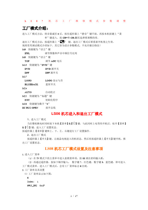
L S07机芯工厂维修模式参数调整工厂模式介绍:进入工厂模式方法:将音量减至0后,按住遥控器上“静音”键不放,再按本机按键上“菜单”键进入。
按CH+和CH-翻页选择要调整的项。
退出工厂模式方法:按遥控器上“”键,退出工厂模式后要重新开机使之生效。
现将常用调试模式介绍如下,其它皆为设计参数模式,不允许擅自修改!M6快捷键为“语言”键IFPL 调节图像和声音中频信号比列M6快捷键为“语言”键TOP 调节AGC电压M13快捷键为“DVD”键DVD DVD源开关DPF DPF源开关M17LOGO LOGO显示与否BLUEBACK 蓝屏开关M24AUTO 自动校正M25快捷键为“标题”键INIT初始化程序M28快捷键为数字“0”IIC BUS OPEN 放开总线LS06机芯进入和退出工厂模式1、进入工厂模式当在整机断电时同时按下本机【菜单】&【】键,与此同时上电等待开机后,松开【菜单】&【】键,进入工厂设置状态。
按遥控器上【菜单】键和上、下、左、右键进行工厂设置操作。
2、退出工厂模式按遥控器上【开关】键,让液晶电视进入待机状态,然后再按遥控器上【开关】键开机,推出工厂设置状态。
LS08机芯工厂模式设置及注意事项1.进入工厂菜单(1)在TV模式下的主菜单中进入童锁菜单项,按OK调出密码输入框;(2)再通过遥控器,按如下顺序输入:数字键7,红色键,数字键9,蓝色键,即可进入工厂模式菜单。
进入工厂模式后,会有工厂菜单标志M出现。
2.工厂菜单及其设置⑴工厂菜单显示如下图:MIndex: 1HWUC_BRI 0x1F其中字母M表示当前进入了工厂模式,Index后面的数字代表当前调节的索引号,HWUC_BRI 表示当前调节项的名称,0X1F表示其数值。
每个调节项目都有唯一的索引号与之对应,操作人员直接按数字键或按P+/P-。
⑵可以选择调节的项目,索引号与调节项目对应关系如下图:注意:1、如没有特殊要求,请不要进入第20项(设计模式);2、第16项调整时会清空存储的数据,因此,若非必须请不要调动,索引号为1、2、3、4、5、6的项一般不需要调节。
友达奇美液晶屏命名规则
虎将科技(深圳)有限公司监视器|广告机|投影机|安防设备制造商|友达光电产品命名规则友达光电,简称Auo ,命名规则:B121EW01,B170PW03第一位表示用途,2-4位为尺寸,5位为分辨率,6位为宽屏/普屏(在非a-Si 技术中标注所用技术),最后两位为产品代次,注:部分产品还有空格后加注V*(如B121EW07 V0) 还没有弄明白其含义。
具体细明如下: 第一位表示用途 B ;表示笔记型电脑用 G :表示工业用 T :表示电视用 M :表示桌上电脑用 H :表示手机用 C :表示车载设备用A :表示可移动产品(数码相机,PDA 等) 第二到四位表示尺寸例如:121代表12.1’ 170代表17’ 第五位表示分辨率 I :128*128 Q :320*240 A :280*220 B :640*240C :160*234 /480*240虎将科技(深圳)有限公司监视器|广告机|投影机|安防设备制造商|D :960*240 F :480*234 V :640*480 S :1680*1050E :1280*800 P :1440*900X :1024*768 1366*768 H :1920*1080 U :1920*1200注:因为产品太多,目前总结这些 可能有遗漏。
第六位表示普通屏幕和宽屏 N :普通型 W :宽屏型另外:在不用a-Si 屏的情况下它代表所用技术 L/T::代表低温多晶硅技术 七八位表示产品代数:例如:01表示第一代产品,03表示第三代产品部分产品加空格后还有第九、十位,这个还没有弄明白其所代表的含义。
下面是AU 部分产品名称及其对应型号用途说明。
笔记本电脑Wide Aspect Ratio ModelSizeResolution虎将科技(深圳)有限公司监视器|广告机|投影机|安防设备制造商|B121EW01 12.1" WXGA (1280 x 800) B121EW03 12.1" WXGA (1280 x 800) B121EW04 12.1" WXGA (1280 x 800) B121EW07 V0 12.1" WXGA (1280 x 800) B133EW01 13.3" WXGA (1280 x 800) B141EW02 14.1" WXGA (1280 x 800) B141PW01 14.1" WXGA+ (1440 x 900) B154EW02 V1 15.4" WXGA (1280 x 800) B154PW04 V0 15.4" WXGA+ (1440 x 900) B170PW03 17'' WXGA+ (1440 x 900) B170PW07 17" WXGA+ (1440 x 900) B170UW02 17" WUXGA (1920 x 1200) B170UW02 V0 17"WUXGA (1920 x 1200)Standard Aspect Ratio Model Size Resolution B141XG09 V3 14.1" XGA (1024 x 768) B150XG02 V415''XGA (1024 x 768)液晶电视虎将科技(深圳)有限公司监视器|广告机|投影机|安防设备制造商|Model Size ResolutionT370HW02 37" Full HD (1920 x 1080) T420HW01 42" Full HD (1920 x 1080) T420HW01 V3 42" Full HD (1920 x 1080) T460HW02 46" Full HD (1920 x 1080) T645HW01 65Full HD (1920 x 1080)HD Model Size Resolution T200XW02 20" WXGA (1366 x 768) T230XW01 23" WXGA (1366 x 768) T260XW02 26" WXGA (1366 x 768) T315XW01 32" WXGA (1366 x 768) T315XW02 32" WXGA (1366 x 768) T370XW01 37" WXGA (1366 x 768) T370XW02 37" WXGA (1366 x 768) T420XW0142"WXGA (1366 x 768)桌上型电脑Wide Aspect Ratio Model Size Resolution M185XW01 V0 18.5" 1366 x 768M190PW01 V0 19" WXGA+ (1440 x 900) M201EW02 V8 20.1" WSXGA+ (1680 x 1050) M215HW01 V0 21.5" 1920 x 1080M220EW01 V0 22" WSXGA+ (1680 x 1050) M240UW04 V0 24" WUXGA (1920 x 1200) M240HW01 V0 24"1920 x 1080Standard Aspect Ratio ModelSizeResolution虎将科技(深圳)有限公司监视器|广告机|投影机|安防设备制造商|M170EG01 VD17SXGA (1280 x 1024一般工业用显示器G057QN01 5.7 QVGA (320 x 240) G057VN01 5.7 VGA (640 x 480) G065VN01 V0 6.5 VGA (640 x 480) G065VN01 V1 6.5 VGA (640 x 480) G084SN03 V1 8.4 SVGA (800 x 600) G084SN05 V7 8.4 SVGA (800 x 600) G104VN01 10.4 VGA (640 x 480) G104SN02 V1 10.4 SVGA (800 x 600) G104SN03 V1 10.4 SVGA (800 x 600) G121SN01 V1 12.1 SVGA(800x600) G121SN01 V3 12.1 SVGA (800x600) G150XG01 V1 15 XGA (1024 x 768) G150XG02 V0 15 XGA (1024 x 768) G150XG03 V2 15 XGA (1024 x 768) G420XW01 V0 42 WXGA (1366 x 768) G420XW02 V0 42 WXGA (1366 x 768) P645HW01 V0 65 FHD (1920 x 1080) P520HW01 V0 52 FHD (1920 x 1080) G220SW01 V0221680 x 1050移动电话Model Size Resolution H016IN01 1.56" 128 R.G.B. x 128 H167IN01 1.67" 128 R.G.B. x 160 H176HN01 1.76" 176 R.G.B. x 220 H177IN01 1.77" 128 R.G.B. x 160 H177IN021.77"160 R.G.B. x 128虎将科技(深圳)有限公司监视器|广告机|投影机|安防设备制造商|H019HN01 1.88" 176 R.G.B. x 220 H200HN01 2.0" 176 R.G.B. x 220 H283QN012.83"240 R.G.B. x 320LTPS ModelSizeResolutionH180QT01 1.8" 240 R.G.B. x 320 H200QT01 2.0" 240 R.G.B. x 320 H220QT02 2.2" 240 R.G.B. x 320 H222QL01 2.22" 240 R.G.B. x 320 H241QL01 2.4" 240 R.G.B. x 320 H283VL012.83"VGA 480 R.G.B. x 640数码相机 摄象机A015AN04 1.5" 280 x 220 A017CN01 1.7" 480 x 240 A020CN01 2.0" 480 x 240 A020BL01 2.0" LTPS 640 x 240 A024CN02 2.4" 480 x 234 A025BN01 2.5" 640 x 240 A025DL02 2.5'' LTPS 960 x 240 A027CW00 2.7" 480 x 234 A027DL01 2.7" LTPS 960 x 240 A027DN01 2.7" 960 x 240 A030DL01 3.0" LTPS 960 x 240 A030DL023.0" LTPS960 x 240车载产品C036QN02 3.6" 320 R.G.B. x 240 C065GW01 6.5" 400 R.G.B. x 234 C065VL016.5"800 R.G.B. x 480虎将科技(深圳)有限公司监视器|广告机|投影机|安防设备制造商|C070FW01 7.0" 480 R.G.B. x 234 C070VW02 7.0" 800 R.G.B. x 480 C080VW028.0"800 R.G.B. x 480Portable Media Player Model Size Resolution A036QN02 3.6 320 R.G.B. x 240 A070FW03 7.0" 480 R.G.B. x 234 A070VW02 7.0" 800 R.G.B. x 480 A085FW01 8.5" 480 R.G.B. x 234 A102VW0110.2"800 R.G.B. x 480一般应用Model Size Resolution A035CN02 3.5" 160 R.G.B. x 234 A040CN01 4.0" LED 160 R.G.B. x 234 A056DN015.6"320 R.G.B. x 234奇美电子产品命名规则奇美电子,简称CMO ,命名规则分两种1,大尺寸2,中小尺寸大尺寸命名规则第一位表示用途,第二位到四位为尺寸,第五位为分辨率,最后一位为产品代次,共六位,部分产品还有空格后加七八九位。
G057VN01.2_友达5.7寸液晶屏-杭州旭虹科技有限公司

Preliminary SpecificationFinal SpecificationModule 5.7 Inch Color TFT-LCD Model Name G057VN01 V2Customer DateChecked &Approved byNote: This Specification is subject to change without notice.Approved by DateDebbie Chiu 2011/10/18Prepared byDaniel PY Tsai2011/10/18 General Display Business Division / AU Optronics corporationContents1. Operating Precautions (4)2. General Description (5)2.1 Display Characteristics (5)2.2 Optical Characteristics (6)3. Functional Block Diagram (8)4. Absolute Maximum Ratings (9)4.1 Absolute Ratings (9)4.2 Absolute Ratings of Environment (9)5. Electrical Characteristics (10)5.1 TFT-LCD Driving (10)5.2 Backlight Unit Driving (11)6. Signal Characteristic (12)6.1 Pixel Format Image (12)6.2 Scanning Direction (12)6.3 The Input Data Format (13)6.4 TFT- LCD Interface Signal Description (15)6.5 TFT- LCD Interface Timing (16)6.6 LED Backlight Unit Interface Signal Description (17)6.7 Power ON/OFF Sequence (17)7. Connector & Pin Assignment (18)7.1 TFT- LCD Signal (CN1): LCD Connector (18)7.2 LED Backlight Unit (CN2): Backlight Connector (18)7.3 PIN 1 definition of CN1 and CN2 (20)8. Reliability Test Criteria (20)9. Mechanical Characteristics (22)10. Label and Packaging (23)10.1 Shipping Label (on the rear side of TFT-LCD display) (23)10.2 Carton Package (23)11 Safety (24)11.1 Keen Edge Requirements (24)11.2 Materials (24)11.3 Capacitors (24)11.4 National Test Lab Requirement (24)Record of RevisionVersion and Date PageOld description New DescriptionRemark0.1,May, 05, 2011AllFirst edition preliminary specifications 5Typical Power Consumption = TBD Typical Power Consumption =3.74W (LCD:0.5W/LED BLU: 3.24W)@ All black pattern, Full Load and V LED =12V5Weight = TBDWeight = 150g (typ.), 165g (max.)6Color / Chromaticity Coordinates =TBDUpdate Chromaticity Coordinates10VDD Power = TBD VDD Power = Typ. 0.5 w Max. 0.55 w11Input Current = TBDPower Consumption = TBD Input Current = 0.27 APower Consumption = 3.24 w 187.3 PIN 1 definition of CN1 and CN2Update 2D drawing 209. Mechanical Characteristics Update 2D drawing1.0 Oct.,03 201111161819Parameter guideline for LED Timing CharacteristicsConnector & Pin Assignment Connector & Pin Assignment Add LED backlight parameter Add Setup & Hold TimeAdd LED Light Bar Input (CN3)Add PIN 1 definition of CN31.1 Nov.22, 201121Assembly Module DrawingAdd CN2 coordinate1.2 Dec.11, 201411Update paremetr guideline of LED1. Operating Precautions1)Display area (Polarizer) of TFT-LCD Module is easily to be damaged, please be cautious and notto scratch it.2)Be sure to power off your machine before connecting or disconnecting your signal cable toTFT-LCD Module.3)Wipe off water drop on display area immediately.Long contact with water may causediscoloration or spots.4)When the panel surface is soiled, wipe it with absorbent cotton or soft cloth.5)Display area (Glass) of TFT-LCD Module may be broken or cracked if bump Module against hardobject.6)To avoid ESD (Electro Static Discharge) damage, be sure to ground yourself before handlingTFT-LCD Module.7)Do not open nor modify the TFT-LCD module assembly.8)Do not press the reflector sheet at the back of the module to any direction.9)In case if TFT-LCD module has to be put back into the packing container slot after it was takenout from the container, do not press the center of the LED Reflector edge. Instead, press at the far ends of the LED Reflector edge softly. Otherwise the TFT-LCD Module may be damaged. 10)When inserting or removing of your signal cable to TFT-LCD Module, be sure not to applyabnormal force (rotate, tilt…etc.) to the Connector of the TFT-LCD Module.11)TFT-LCD Module is not allowed to be twisted & bent even force is added on module in a veryshort time. Please design your display product well to avoid external force applying to module by end-user directly.12)Small amount of materials without flammability grade are used in the TFT-LCD module. TheTFT-LCD module should be supplied by power complied with requirements of Limited Power Source (IEC60950 or UL1950), or be applied exemption.13)Severe temperature condition may result in different luminance, response time.14)Continuous operating TFT-LCD Module under high temperature environment may accelerateLED light bar exhaustion and reduce luminance dramatically.15)The data on this specification sheet is applicable when TFT-LCD module is placed in landscapeposition.16)Continuous displaying fixed pattern may induce image sticking. It’s recommended to use screensaver or moving content periodically if fixed pattern is displayed on the screen.2. General DescriptionG057VN01 V2 is designed for industrial display applications with VGA (640 x RGB x480) resolution and 262k colors (RGB 6-bits).It is composed of a TFT-LCD panel, driver ICs, control and power supply circuits board and backlight unit including LED driver circuit.G057VN01 V2 offers CMOS interface for display signal input.2.1 Display CharacteristicsThe following items are G057VN01 V2characteristics summary at 25 (Room Temperature).Items Unit SpecificationsScreen Diagonal inch 5.7Active Area mm115.2(H) x 86.4(V)Pixels H x V640x3(RGB) x 480Pixel Pitch mm0.18 x 0.18Pixel Arrangement R.G.B. Vertical StripeDisplay Mode TN, Normally WhiteNominal Input Voltage VDD Volt 3.3 typ.Typical Power Consumption Watt 3.74W (LCD:0.5W/LED BLU: 3.24W)@ All black pattern, Full Load and V LED=12VWeight Grams150g(typ.), 165g (max.)Physical Size mm144.0(H)x 104.6(V) x 12.3(D) (typ.) Electrical Interface CMOS 6-bit Parallel RGB Surface Treatment Anti-Glare, Hardness 3HSupport Color262K colorsThe most suitable view angle12 o’clockTemperature RangeOperatingStorage (Non-Operating)o Co C-30 to +85-30 to +85RoHS Compliance RoHS Compliance2.2 Optical CharacteristicsThe optical characteristics are measured under stable conditions at 25 (Room Temperature).ItemUnit ConditionsMin.Typ.Max.Remark White Luminance cd/m2V LED =12V, D PWM =100%(center point)525700-Note 1Uniformity %5 Points- 1.3Note 1, 2, 3Contrast Ratio500800-Note 4msecRising -1520msec Falling -1015Response Timemsec Rising + Falling -2535Note 5degree degree Horizontal (Right)CR = 10 (Left)70708080--Viewing Angledegree degreeVertical (Upper)CR = 10 (Lower)60607070--Note 6White x 0.2630.3130.363White y 0.2790.3290.379Red x0.4990.5490.599Red y 0.2640.3140.364Green x 0.2790.3290.379Green y 0.5480.5980.648Blue x 0.1060.1560.206Color / Chromaticity Coordinates (CIE 1931)Blue y0.0680.1180.168Color Gamut%-50-Note 1: Measurement methodEquipment Pattern Generator, Power Supply, Digital Voltmeter, Luminance meter (SR_3 or equivalent)Aperture1with 50cm viewing distance∘Test Point Center Environment < 1 luxLCD ModuleSR_3 or equivalentmeasuring distanceModule Driving EquipmentNote 2: Definition of 5 points position (Display active area: 115.2mm(W) x 86.4mm(H))Note 3:The luminance uniformity of 5 points is defined by dividing the maximum luminance value by the minimum luminance value at full white condition.Note 4: Definition of contrast ratio (CR):Note 5: Definition of response time:The output signals of photo detector are measured when the input signals are changed from “White” to “Black” (falling time) and from “Black” to “White” (rising time), respectively. The response time interval definition is between 10% and 90% of amplitude. Please refer to the figure as below.Maximum Brightness of five pointsW5 =Minimum Brightness of five pointsContrast ratio (CR)=Brightness @ “White” state Brightness @ “Black” stateNote 6: Definition of viewing angleViewing angle is the measurement of contrast ratio 10, at the screen center, over 180° horizontal and 180° vertical range. The180° horizontal(θL, θR) and 180° vertical(ΦH, ΦL) range are illustrated as following figure.3.Functional Block DiagramThe following diagram shows the functional block of the G057VN01 V2 color TFT/LCD module.4. Absolute Maximum Ratings4.1 Absolute RatingsItem Symbo Min Max Unit Remark Logic/LCD Drive Voltage VDD-0.3+3.6Volt Ta= 25o C LCD Input Signal Voltage VIN-0.3+3.6Volt Ta= 25o C LED BLU Drive Voltage V LED023Volt Ta= 25o C LED Dimming Input VoltageV PWM08Volt Ta= 25o C High4.2 Absolute Ratings of EnvironmentItem Symbol Min Max Unit Remark Operating Temperature TOP-30+85 Note 1, 2 Operation Humidity HOP595%RH Note 1, 2 Storage Temperature TST-30+85 Note 1Storage Humidity HST595%RH Note 1tion.Note 1: Maximum Wet-Bulb should be39and no condensaNote 2:Only operation is guaranteed. Optical performance should be evaluated at 25 only.5. Electrical Characteristics5.1 TFT-LCD Driving5.1.1 Power SpecificationSymbol ParameterMin Typ Max Units RemarkVDD Logic/LCD Drive Voltage 3.0 3.3 3.6Volt IDD VDD Current -140155mA All Black Pattern (VDD=3.3V, at 60Hz)I rush LCD Inrush Current -- 1.5A Note 1PDD VDD Power-0.50.55WattAll Black Pattern (VDD=3.3V, at 60Hz)VDDrpAllowable Logic/LCD Drive Ripple Voltage --100mVp-pAll Black Pattern (VDD=3.3V, at 60Hz)Note 1: Measurement condition:Q3AO6402GD 2SD 1D 5D 6Q3AO6402GD2SD1D5D6C11uF/16VC21uF/25VC30.01uF/25VF1VR147K+12.0VVCCSW1SW MAG-SPST12(High to Low)Control Signal(LCD Module Input)R21K+3.3VR147KR21K90%10%VDD rising time0V3.3V0.5msVDD5.1.2 Signal Electrical CharacteristicsInput signals shall be low or Hi-Z state when VDD is off.Parameter Symbol Min.Typ.Max.Unit RemarksHigh VIH0.7VDD-VDD VoltLogic Input Voltage forDisplay Signals Low VIL0-0.3VDD VoltHigh VIH0.7VDD-VDD VoltInput Voltage for RL/UDLow VIL0-0.3VDD Volt5.2 Backlight Unit Driving5.2.1 Parameter guideline for LEDom Temperature) Following characteristics are measured under stable condition using a LED driving board at 25(Ro Symbol Parameter Min Typ Max Units RemarkV LED Input Voltage91220VoltI LED Input Current-0.270.297A V LED =12V, D PWM =100%P LED Power Consumption- 3.24 3.56Watt V LED =12V, D PWM =100%I rush LED Inrush Current- 1.5A V LED =12V, D PWM =100%Dimming control Voltage High 2.0 3.3 5.5VoltV PWM DIMDimming control Voltage Low--0.2VoltNote 1,2F PWM Dimming Frequency20030K HzD PWM Dimming duty cycle1100%On Control Voltage2 3.3 5.5VoltV LED On/OffNote 3, 4Off Control Voltage--0.8VoltI F LED Forward Current80mA Ta = 25oCV F LED Forward Voltage35.040.0IF = 80mA, Ta = 25oC P LED LED Power 2.8 3.2WattOperating Life50000--Hrs Note 5, 6Note 1: PWM dimming function can be operated by PWM signal. PWM duty cycle can adjust white Luminance.(PWM High: ON and PWM Low: OFF)Note 2: PWM signal can not be floating and pull-down to ground when waiting.Note 3: Enable (V LED On/Off) must be turned on late than V LED and PWM Signal.Note 4: Enable (V LED On/Off) must be turned off early than V LED and PWM Signal.Note 5: If G057VN01 V2module is driven by high current or at high ambient temperature & humidity condition.The operating life will be reduced.Note 6: Operating life means brightness goes down to 50% initial brightness. Minimum operating life time is estimateddata.Note 7: See Section 6.6 for LED Backlight Unit Interface Signal Description6. Signal Characteristic6.1 Pixel Format ImageFollowing figure shows the relationship between input signal and LCD pixel format.6.2 Scanning DirectionThe following figures show the image seen from the front view. The arrow indicates the direction of scan.Note1: TFT-LCD interface signal description is shown in section 6.4.6.3 The Input Data FormatThis product displays 262,144colors in terms of the 64 grey levels on RGB respectively. The following table demonstrates the display of input data.6.4 TFT- LCD Interface Signal DescriptionNote 1: “Low” stands for 0V. “High” stands for 3.3V. “NC” stands for ”No Connection”.6.5 TFT- LCD Interface Timing6.5.1 Timing Characteristics DE mode onlySignal Symbol Min.Typ.Max.Unit Remark Clock frequency (DOTCLK)1/ T CLOCK 23.925.234.2MHz Note1Setup Time Tdsu 8--ns DataHold TimeTdhd 8--ns RL,GL,BL to DCLKDESetup Time Tesu 8--nsPeriod T H 7708001000Active T HD 640Horizontal SectionBlankingT HB 130160360T CLOCKNote1Period T V 516525570Active T VD 480Vertical SectionBlankingT VB364590T LINENote1Note 1: Recommended frame rate is 60 Hz.6.5.2 Input Timing DiagramDOTCLKDET HT HBT HDDET VDInput Timing Definition ( DE Mode)T CLOCKInput Data Invaild Data Invaild Data6.6LED Backlight Unit Interface Signal DescriptionPin #Symbol Pin Description1V LED12V input2V LED12V input3GND Ground4GND Ground5PWM DIM1~100% PWM dimming6LED On/Off0V-Off; 3.3~5V/NC-OnNote 1: “NC” stands for ”No Connection”6.7 Power ON/OFF SequenceVDD power, LCD interface signals and backlight on/off sequence are shown in the following chart. Signals from any system shall be Hi-Z state or low level when VDD is off.Power ON/OFF sequence timingON/OFF sequence should be applied to avoid abnormal function in the display. Please make sure to turn off the power when you plug the cable into the input connector or pull the cable out of the connector.7. Connector & Pin Assignment7.1 TFT-LCD Signal (CN1): LCD ConnectorManufacturer Starconn089H33-000100-G2-R, compatible with Connector Model NumberIMSA-9637S-33Y902 & ELCO08-6210--033-340-800+ Pin#Symbol Pin#Symbol Pin#Symbol1GND12GND23B32DOTCLK13G024B43NC14G125B54NC15G226GND5GND16G327DE6R017G428VDD7R118G529VDD8R219GND30R/L9R320B031U/D10R421B132NC11R522B233GND 7.2 LED Backlight Unit (CN2): Backlight ConnectorManufacturer JSTSM06B-SRKS-G-TBConnector Model Numbercompatible with JST SM06B-SRSS-TB (LS) (SN) Mating Connecter Model Number JST SHR-06V-BKHF-B or compatiblePin #Symbol Pin #Symbol1V LED4GND2V LED5PWM DIM3GND6LED ON/OFF7.3 LED Light Bar Input (CN3): Light Bar ConnectorManufacturer STM or compatibleConnector Model Number P24021P6 or compatibleMating Connecter Model Number SM06B-SHLS-TF or compatiblePin #Symbol Pin Description Cable color 1AN1Channel 1 LED anode Red2AN2Channel 2 LED anode Red3AN3Channel 3 LED anode Red4CA1Channel 1 LED cathode White5CA2Channel 2 LED cathode Blue6CA3Channel 3 LED cathode Black7.4PIN 1 definition of CN1 and CN2(Rear side of TFT-LCD )7.5PIN 1 definition of CN38. Reliability Test CriteriaCN2CN1CN380 5G057VN01 V2Items Required Condition Remark Temperature Humidity Bias40/90%,300HrNote 2 High Temperature Operation85,300HrNote 2 Low Temperature Operation-30,300HrNote 2 High Temperature Storage85,300hoursNote 2 Low Temperature Storage-30 ,300 hours Note 2 Thermal Shock Test-20 /30 min ,60 /30 min ,100cycles Note 2 Hot Start Test 85 /1 Hr (min.), power on/off per 5 minutes, repeat 5 times Note 2 Cold Start Test-30 /1 Hr (min.), power on/off per 5 minutes, repeat 5 times Note 2 Shock Test(Non-Operating)50G,20ms,Half-sine wave, (±X, ±Y, ±Z)Note 2 Vibration Test(Non-Operating)1.5G, 10~200~10Hz, Sine wave, 30mins/axis, 3 direction (X, Y, Z)Note 2ESD Contact Discharge: ±8KV, 150pF(330Ω) 1sec, 8 points, 25 times/pointAir Discharge: ±15KV, 150pF(330Ω) 1sec, 8 points, 25 times/pointNote 1,2Attitude Test Operating: 14,000 ft, Ramp: 2000 ft/min, 8hrsNon-operating: 40,000 ft, Ramp: 2000 ft/min, 24hrsNote 2Note1: According to EN61000-4-2 ESD class B criteria, some performance degradation is allowed. TFT-LCD module is self-recoverable,no data lost and no hardware failures after test.Note2:●Water condensation is not allowed for each test items.●Each test is done by new TFT-LCD module. Don’t use the same TFT-LCD module repeatedly for reliability test.●The reliability test is performed only to examine the TFT-LCD module capability.●To inspect TFT-LCD module after reliability test, please store it at room temperature and room humidity for 24hours at least in advance.工业液晶屏http://www.hzxuhonglcd.com/10. Label and Packaging10.1 Shipping Label(on the rear side of TFT-LCD display)10.2 Carton PackageMax. capacity: 60 pieces TFT-LCD module per cartonMax. weight: 12.95 kg per cartonOutside dimension of carton: 520(L)mm* 340(W)mm* 250(H)mm11 Safety11.1 Keen Edge RequirementsThere will be no keen edges or corners on the display assembly that could cause injury.11.2 Materials11.2.1 ToxicityThere will be no carcinogenic materials used anywhere in the TFT-LCD module. If toxic materials are used, they will be reviewed and approved by the responsible AUO toxicologist.11.2.2 FlammabilityAll components including electrical components that do not meet the flammability grade UL94-V1 in the TFT-LCD Module will complete the flammability rating exception approval process.The printed circuit board will be made from material rated 94-V1 or better. The actual UL flammability rating will be printed on the printed circuit board.11.3 CapacitorsIf any polarized capacitors are used in the TFT-LCD module, provisions will be made to keep them from being inserted backwards.11.4 National Test Lab RequirementThe TFT-LCD Module will satisfy all requirements for compliance to UL 60950 (U.S.A. Information Technology Equipment).。
G050VVN01.0,广视角友达液晶屏,5寸友达屏

5英寸
点分辨率
480(RGB)* 800(WXGA)
像素密度
188PPI
像素排列
RGB垂直条状
宽高比
3:5(宽:高)
点间距
0.045*0.135mm(横*竖)
像素间距
0.135*0.135mm(横*竖)
液晶屏重量
48.0g(Max.)
表面处理
雾面,Hard coating(3H)
显示区域
64.8*108.0mm(横*竖)
G050VVN01.0
一:友达5寸工业液晶屏G050VVN01.0基本信息
品牌
友达(AUO)
面板型号
G050V度
-10 ~ 80°C
作业湿度
5-95 (%RH)
保存湿度
5-95 (%RH)
当前生产状态
停产中
二:友达5寸工业液晶屏G050VVN01.0结构特征
响应时间
20/15(Typ.)(Tr/Td)(ms)
可视角度
80/80/80/80 (Typ.)(CR≥10) (左/右/上/下)
最佳视角
上下左右对称
四、友达5寸工业液晶屏G050VVN01.0发光系统
灯管位置
侧入式光源
光源类型
WLED
外观尺寸
71.2*119.5mm(横*竖)
外观尺寸
2.50±0.2 mm (厚度)
触摸屏
无
三:友达5寸工业液晶屏G050VVN01.0光学特征
显示模式
MVA,常黑显示,透射式
液晶屏亮度
450cd/m2 (Typ.)
对比度
700:1 (Typ.) (透射)
显示颜色
16.7M(8-bit )
友达全视角7寸工业液晶屏-G070VVN01.2 工控屏
LCD液晶屏: 友达全视角7寸工业液晶屏-G070VVN01.2 工控屏品牌友达(AUO)面板型号G070VVN01.2工作温度-20 ~70°C存储温度-30 ~ 80°C作业湿度5-95 (%RH)保存湿度5-95 (%RH)当前生产状态量产中液晶屏尺寸7英寸点分辨率800(RGB)*480(WXGA)像素密度133PPI像素排列RGB垂直条状宽高比15:9(宽:高)点间距0.0635*0.1905mm(横*竖)像素间距0.1905*0.1905mm(横*竖)液晶屏重量143g(Typ.)表面处理雾面,Hard Coating(3H)显示区域152.4*91.44mm(横*竖)可视区域154.2*93.2mm(横*竖)外观尺寸164.55*104.71mm(横*竖)外观尺寸8.5(Max.) mm (厚度)触摸屏带触摸屏(投射电容屏)显示模式MVA,常黑显示,透射式液晶屏亮度600cd/m2 (Typ.)对比度1500:1 (Typ.) (透射)显示颜色262K/16.2M (6-bit / 6-bit + FRC)显示色域70%NTSC(CIE1931)响应时间10/25(Typ.)(Tr/Td)(ms)可视角度80/80/80/80 (Typ.)(CR≥10) (左/右/上/下) 最佳视角全视角白色色度X:0.311; Y:0.328白场变动 1.25 (Max.)(9 points)灯管位置侧入式光源光源类型WLED灯管数量7S2P灯管形状阵列灯管数量 4 strings光源寿命30K(Min.)(小时)单灯电压22.4/25.2V(Typ./Max.)单灯电流120mA(Typ.)灯管功率总耗 2.69/3.03W (Typ./Max.)背光电路无信号大类TTL信号小类Parallel RGB(1 ch, 6/8-bit)面板电压 3.3V (Typ.)面板电流160/197mA (Typ./Max)面板功率528/650mW(Typ./Max)接口类型端子接口脚距 1.25 mm接口数量 1 pcs接口脚数20 pins●补充说明:以上资料仅供参考,如有某项不准确,可以联系我们客服提供产品的规格资料,产品均以pdf规格为准。
NJ070NA-23A 群创7寸液晶屏-杭州旭虹科技

INNOLUX DISPLAY CORPORATIONLCD MODULESPECIFICATIONCustomer:Model Name: NJ070NA-23ADate: 2017/02/27Version: 01□Preliminary Specification■Final SpecificationFor Customer’s AcceptanceApproved by CommentApproved by Reviewed by Prepared byCs.Chang Henry.Chien 2016/12/27 Cc01.ChenWenguo.DengSunny.Sun2016/12/27Rong.Ye2016/12/27InnoLux copyright 2016All rights reserved,Copying forbidden.Record of RevisionVersion Revise Date Page ContentPre-Spec.V01 2014/04/15 All Initial Release.Pre-Spec.V02 2014/12/23 1 Update Backlight power consumption& Panel power consumption& Weight5 Update Operation Specifications6 Update Input signal voltage7 Update Current Consumption& Backlight Driving Conditions13 Update Optical Specifications20 Update Packaging Material TablePre-Spec.V03 2015/01/09 7 Update Current Consumption18 Update Safety19 Modify Mechanical Drawing21 Modify Package DrawingFinal-Spec 2015/04/20 First Final Release for P070BAG-CM119 Modify Mechanical Drawing2016/01/07 19 Modify Mechanical Pixel size.Final-Spec-V01 2016/12/271 Model name change from P070BAG-CM1 to NJ070NA-23AFinal-Spec-V02 2017/02/27 20 Modify Reliability Test ItemINNO L U XContents1. General Specifications (1)2. Pin Assignment (2)3. Operation Specifications (5)3.1. Absolute Maximum Ratings (5)3.1.1. Typical Operation Conditions (6)3.1.2. Current Consumption (7)3.1.3. Backlight Driving Conditions (7)3.2. Power Sequence (8)3.3. Timing Characteristics (9)3.3.1. AC Electrical Characteristics (9)3.3.2. Input Clock and Data Timing Diagram (9)3.3.3. DC Electrical Characteristics (10)3.3.4. Timing (11)3.3.5. Data Input Format (12)4. Optical Specifications (13)5. Reliability Test Items (17)6. General Precautions (18)6.1. Safety (18)6.2. Handling (18)6.3. Static Electricity (18)6.4. Storage (18)6.5. Cleaning (18)7. Mechanical Drawing (19)8. Package Drawing (20)8.1. Packaging Material Table (20)8.2. Packaging Quantity (20)8.3. Packaging Drawing (21)1. General SpecificationsThe specification NJ070NA-23A is a 7 ”(1024x600) TFT Liquid Crystal Display module with LED Backlight unit , 40 pin LVDS interface, normally white transmissive display mode. This module will be applied to Consumer Electronics(CE Application)No. Item Specification Remark1 LCD size 7.0 inch(Diagonal)2 Driver element a-Si TFT active matrix3 Resolution 1024 × 3(RGB) × 6004 Display mode Normally White, Transmissive5 Pixel size 0.1506(W) × 0.1432(H) mm6 Active area 154.2144(W) × 85.92(H) mm7 Module size 164.9(W) ×100(H) ×4.8(D) mm Note 18 Surface treatment Hard Coating9 Color arrangement RGB-stripe10 Interface LVDS11 View direction(Gray Inversion) 6 O’Clock12 Backlight power consumption 2.62 W (Typ.)13 Panel power consumption 0.4 W (Typ.)14 Weight 140g (Typ.)15 Source Driver IC NT51008QH-D/3EA16 Gate Driver IC NT52003BH-D/3EBNote 1: Refer to Mechanical Drawing.2. Pin AssignmentFPC Connector is used for the module electronics interface. The recommended model is FH12A-40S-0.5SH manufactured by Hirose.Pin No. Symbol I/O Function Remark1 VCOM P Common Voltage2 VDD P Power Voltage for digital circuit3 VDD P Power Voltage for digital circuit4 NC --- No connection5 Reset I Global reset pin6 STBYB I Standby mode, Normally pulled high STBYB = “1”, normal operation STBYB = “0”, timing controller, source driver will turn off, all output are High-Z7 GND P Ground8 RXIN0- I - LVDS differential data input9 RXIN0+ I + LVDS differential data input10 GND P Ground11 RXIN1- I - LVDS differential data input12 RXIN1+ I + LVDS differential data input13 GND P Ground14 RXIN2- I - LVDS differential data input15 RXIN2+ I + LVDS differential data input16 GND P Ground17 RXCLKIN- I - LVDS differential clock input18 RXCLKIN+ I + LVDS differential clock input19 GND P Ground20 RXIN3- I - LVDS differential data input21 RXIN3+ I + LVDS differential data input22 GND P Ground23 NC --- No connection24 NC --- No connection25 GND P Ground26 NC --- No connection27 DIMO O Backlight CABC controller signal output28 SELB I 6bit/8bit mode select Note129 AVDD P Power for Analog Circuit30 GND P Ground31 LED- P LED Cathode32 LED- P LED Cathode33 L/R I Horizontal inversion Note334 U/D I Vertical inversion Note335 VGL P Gate OFF Voltage36 CABCEN1 I CABC H/W enable Note237 CABCEN0 I CABC H/W enable Note238 VGH P Gate ON Voltage39 LED+ P LED Anode40 LED+ P LED AnodeI: input, O: output, P: PowerNote1: If LVDS input data is 6 bits ,SELB must be set to High;If LVDS input data is 8 bits ,SELB must be set to Low.Note2: When CABC_EN=”00”, CABC OFF.When CABC_EN=”01”, user interface image.When CABC_EN=”10”, still picture.When CABC_EN=”11”, moving image.When CABC off, don’t connect DIMO, else connect it to backlight. Note3: When L/R=”0”, set right to left scan direction.When L/R=”1”, set left to right scan direction.When U/D=”0”, set top to bottom scan direction.When U/D=”1”, set bottom to top scan direction.Note: Definition of scanning direction. Refer to the figure as below:LeftTOPRightBottom3. Operation Specifications3.1. Absolute Maximum Ratings(Note 1)Item SymbolValuesUnit Remark Min. Max.Power voltageDV DD -0.3 5.0 V AV DD 6.5 13.5 V V GH -0.3 42.0 V V GL -20.0 0.3 V V GH-V GL- 40.0 VOperation T emperature T OP -20 70 ℃Storage T emperature T ST-30 80 ℃LED Reverse Voltage V R- 5 VEach LED LED Forward Current I F- 60 mA Each LEDNote 1: The absolute maximum rating values of this product are not allowed to be exceeded at any times. Should a module be used with any of the absolute maximum ratingsexceeded, the characteristics of the module may not be recovered, or in an extremecase, the module may be permanently destroyed.3.1.1. Typical Operation Conditions( Note 1)ItemSymbolValuesUnitRemarkMin.Typ. Max. Power voltageDV DD 3.0 3.3 3.6 V Note 2 AV DD10.81111.2VV GH 19.7 20 20.3 V V GL-6.5 -6.8 -7.1 V Input signal voltage V COM 3.3 3.8 4.3 V Note 4Input logic high voltage V IH 0.7 DV DD- DV DD VNote 3Input logic low voltageV IL-0.3 DV DDVNote 1: Be sure to apply DV DD and V GL to the LCD first, and then apply V GH .Note 2: DV DD setting should match the signals output voltage (refer to Note 3) ofcustomer’s system board.Note 3: LVDS, Reset.Note 4: Typ. V COM is only a reference value, it must be optimized according to each LCM.Be sure to use VR;3.1.2. Current ConsumptionItem SymbolValuesUnit Remark Min. Typ. Max.Current for DriverI GH - 0.26 1 mA V GH =20V I GL - 0.26 1 mA V GL = -6.8V IDV DD - 35 60 mA DV DD =3.3V IAV DD - 20 30 mA AV DD =11V3.1.3. Backlight Driving ConditionsItem SymbolValuesUnit Remark Min. Typ. Max.Voltage for LED backlight V L 8.4 9.9 10.2 V Note 1 Current for LED backlight I L -- 265 -- mALED life time - 20,000 - - Hr Note 2 Note 1: The LED Supply Voltage is defined by the number of LED at Ta=25℃ andI L =265mA.Note 2: The “LED life time” is defined as the module brightness decrease to 50% original brightness at Ta=25℃ and I L =265mA. The LED lifetime could be decreased ifoperating I L is lager than 265mA.3.2. Power Sequencea. Power on:VDD A VGL VGH LVDS Signal B/L VDD A VGL VGH LVDS SignalB/L3.3. Timing Characteristics3.3.1. AC Electrical CharacteristicsParameter SymbolValuesUnit Remark Min. Typ. Max.Clock frequency R xFCLK40.8 51.2 67.2 MHz Input data skew margin T RSKM500 - - ps Clock high time T LVCH- 4/(7* R xFCLK) - ns Clock low time T LVCL- 3/(7* R xFCLK) - ns3.3.2. Input Clock and Data Timing Diagram3.3.3. DC Electrical CharacteristicsParameter SymbolValuesUnit Remark Min. Typ. Max.Differential input high Threshold voltage R xVTH- - +0.1 VR XVCM=1.2VDifferential input lowThreshold voltageR xVTL-0.1 - - V Input voltage range(singled-end)R xVIN0 - 2.4 V Differential input common modevoltageR xVCM|V ID|/2 - 2.4-|V ID|/2 V Differential voltage|V ID|0.2 - 0.6 V Differential input leakage current RV xliz-10 - +10 uA3.3.4. TimingItem SymbolValuesUnit Remark Min. Typ. Max.Clock Frequency fclk 40.8 51.2 67.2 MHz Frame rate =60HzHorizontal display area thd1024 DCLK HS period time th1114 1344 1400 DCLK HS Blanking thb90 320 376 DCLK Vertical display area tvd600 H VS period time tv610 635 800 H VS Blanking thb10 35 200 H3.3.5. Data Input Format6bit LVDS input8bit LVDS inputNote: Support DE timing mode only, SYNC mode not supported.4. Optical SpecificationsItem Symbol ConditionValuesUnit Remark Min. Typ. Max.Viewing angle (CR≥ 10) θLΦ=180°(9 o’clock)65 75 -degree Note 1 θRΦ=0°(3 o’clock) 65 75 -θTΦ=90°(12 o’clock)60 70 -θBΦ=270°(6 o’clock)65 75 -Response timeT ONNormalθ=Φ=0°- 10 20 msec Note 3T OFF - 15 30 msec Note 3 Contrast ratio CR 500 800 - - Note 4Color chromaticity W X 0.26 0.31 0.36 - Note 2Note 5Note 6 W Y 0.28 0.33 0.38 -Luminance L 400 500 - cd/m² Note 6 LuminanceuniformityY U 70 75 - % Note 7Test Conditions:1. DV DD=3.1V, I L=265mA (Backlight current), the ambient temperature is 25℃.2. The test systems refer to Note 2.Fig. 4-1 Definition of viewing angleNote 2: Definition of optical measurement system.The optical characteristics should be measured in dark room. After 30 minutesoperation, the optical properties are measured at the center point of the LCD screen. (Response time is measured by Photo detector TOPCON BM-7, otheritems are measured by BM-5A/Field of view: 1° /Heig ht: 500mm.)Fig. 4-2 Optical measurement system setup6 o’clock directionΦ=0°Φ=180°6 o’clock direction Φ=0°Φ=180°LCMNote 3: Definition of Response timeThe response time is defined as the LCD optical switching time interval between“White” state and “Black” state. Rise time (T ON ) is the time between photo detector output intensity changed from 90% to 10%. And fall time (T OFF ) is the time between photo detector output intensity changed from 10% to 90%.Fig. 4-3 Definition of response timeNote 4: Definition of contrast ratiostate Black"" the on LCD when measured Luminance stateWhite"" the on LCD when measured Luminance (CR) ratio Contrast =Contrast ratio is measured at center point of LCD.Note 5: Definition of color chromaticity (CIE1931)Color coordinates measured at center point of LCD.Note 6: Definition of luminance:Measured at the center area of the panel when LCD panel is driven at “white ” state. The LED driving condition is I L =265mA .90%10% 0%P h o t o d e t e c t o r o u t p u t (R e l a t i v e v a l u e )ONWhite (TFT OFF)Black (TFT ON)White (TFT OFF)Note 7: Definition of Luminance UniformityActive area is divided into 9 measuring areas (Refer to Fig. 4-4 ).Every measuring point is placed at the center of each measuring area.max minB B (Yu)Uniformity Luminance =L-------Active area length W----- Active area widthFig. 4-4 Definition of measuring pointsB max : The measured maximum luminance of all measurement position. B min : The measured minimum luminance of all measurement position.5. Reliability Test ItemsItem Test Conditions Remark High Temperature Storage Ta = 80℃240hrs Note 1,Note3,Note 4,Note5Low Temperature Storage Ta = -30℃240hrs Note 1,Note3,Note 4High Temperature Operation Ts = 70℃240hrs Note 2,Note3,Note 4,Note5Low Temperature Operation Ta = -20℃240hrs Note 1,Note3,Note 4Operate at High Temperature and Humidity +60℃, 90%RH 240hrsNote3,Note 4Note5Thermal Shock [(-30℃30min)→(80℃30min)]/cycle,100cyclesNote3,Note 4Note5Vibration Test Frequency: 10 ~55~10Hz; Sweep Mode: Log SweepSweep time: 1Oct/min; Acceleration: 1.5G; Test time: 2hrs for each direction of X, Y, Z.Mechanical Shock 100G, 6ms, half sine wave, 3 times for each direction of ±X, ±Y, ±ZPackage Vibration Test Random Vibration :ISTA-3A 1Hz~200Hz,Grms=0.53 Half hours for direction of ZPackage Drop Test 72cm(weight≦10kg), 60cm(weight>10kg);1 times for 6-faces, 3-edges and 1-cornerElectro Static Discharge Contact mode:150pf,330Ω,±2KV Air mode:150pf,330Ω,±2KVNote 1: Ta is the ambient temperature of samples.Note 2: Ts is the temperature of panel’s surface.Note 3: In the standard condition, there shall be no practical problem that may affect the display function. After the reliability test, the product only guarantees operation,but don’t guarantee all of the cosmetic specification.Note 4: Before cosmetic and function test, the product must have enough recovery time, at least 2 hours at room temperature.Note 5: A certain level of Mura (non-uniformity) of dark / black image will happen several days after high temperature testing (H.T.T.). There is a slowly part recovery over a long time (several months). Such a long exposure time like in H.T.T. will normally not happen in a real application. Therefore the test H.T.T. was introduced tosimulate cycles with normal conditions in-between but with the same totalexposure time what show a significant reduced Mura.The root cause is related to tension generated due to different amount of shrinking in thestack of layers in the polarizer sheet. The effect is more significant on larger displays likethis size. An investigation into alternative polarizer material showed that there is no better alternative currently available.6. General Precautions6.1. Safety1.Liquid crystal is poisonous. Do not put it in your mouth. If liquid crystal touches yourskin or clothes, wash it off immediately by using soap and water.2.The temperature for use is no more than 80 C, otherwise, only promise the functionis OK, but the quality may be changed.6.2. Handling1. The LCD panel is plate glass. Do not subject the panel to mechanical shock or toexcessive force on its surface.2. The polarizer attached to the display is easily damaged. Please handle it carefullyto avoid scratch or other damages.3. To avoid contamination on the display surface, do not touch the module surfacewith bare hands.4. Keep a space so that the LCD panels do not touch other components.5. Put cover board such as acrylic board on the surface of LCD panel to protect panelfrom damages.6. Transparent electrodes may be disconnected if you use the LCD panel underenvironmental conditions where the condensation of dew occurs.7. Do not leave module in direct sunlight to avoid malfunction of the ICs.6.3. Static Electricity1. Be sure to ground module before turning on power or operating module.2. Do not apply voltage which exceeds the absolute maximum rating value.6.4. Storage1. Store the module in a dark room where must keep at 25±10℃ and 65%RH or less.2. Do not store the module in surroundings containing organic solvent or corrosivegas.3. Store the module in an anti-electrostatic container or bag.6.5. Cleaning1. Do not wipe the polarizer with dry cloth. It might cause scratch.2. Only use a soft sloth with IPA to wipe the polarizer, other chemicals mightpermanent damage to the polarizer.7. M echanical Drawing8. Package Drawing8.1. Packaging Material TableNo. ItemModel(Material)Dimensions(mm)UnitWeight(kg)Quantity(PCS)Remark1 LCM NJ070NA-23A164.90x100x4.8 0.140 502 Dust-Proof BagPE 700 x 530x0.05 0.048 13 CrepePaper_Tape四維CM35 30x10x0.1 0.001 504 CorrugatedBarBC Corrugatedpaper510x122 0.046 45 Partition BC Corrugatedpaper512 × 349 × 226 1.466 16 A/S Bag PE 178*160*0.06 0.004 507 Carton Corrugatedpaper525 × 362 × 250 0.950 18 Total weight 10.12± 5%Kg8.2. Packaging QuantityTotal LCM quantity in Carton: no. of Partition 2 Rows × quantity per Row 25 = 508.3. Packaging Drawing。
AT043TN24 V.7 pre-spec-杭州旭虹科技有限公司

CHIMEI INNO L U X DISPLAY CORPORATIONLCD MODULESPECIFICATIONCustomer: CNSBGModel Name: AT043TN24 V.7SPEC NO.: A043-24-TT-71Date: 2010/04/19Version: 01■Preliminary Specification□Final SpecificationRemark■Touch Screen Panel (3-in-1FPC)■Low Power ConsumptionFor Customer’s AcceptanceApproved by CommentApproved by Reviewed by Prepared byJoe Lin2010/04/24Jack HuangJames YuCharlie Chou2010/04/23Charlie Chou2010/04/23CHIMEI INNO L U XInnoLux copyright 2004All rights reserved,Copying forbidden.Record of RevisionVersion Revise Date Page Content Pre-spec .01 2010/04/19 Initial Release.CHIMEI INNO L U XContents1. General Specifications (1)2. Pin Assignment (2)2.1. TFT LCD Panel Driving Section (2)2.2. Touch Screen Panel Section (3)3. Operation Specifications (5)3.1. Absolute Maximum Ratings (5)3.2. Typical operation conditions (6)3.3 Backlight Driving Conditions (6)3.4. Power Sequence (7)3.5. Timing Characteristics (8)3.5.1. Timing Conditions (8)3.5.2. Timing Diagram (9)4. Touch Screen Panel Specifications (10)4.1. Electrical Characteristics (10)4.2. Mechanical & Reliability Characteristics (11)4.3. Linearity Definition (12)4.4. Housing design guide (13)5. Optical Specifications (14)6. Reliability Test Items (18)7. General Precautions (19)7.1. Safety (19)7.2. Handling (19)7.3. Static Electricity (19)7.4. Storage (19)7.5. Cleaning (19)8. Mechanical Drawing (20)9. Package Drawing (21)9.1. Packaging Material Table (21)9.2. Packaging Quantity (21)9.3. Packaging Drawing (22)1. General SpecificationsNo. Item Specification Remark1 LCD size 4.3 inch(Diagonal)2 Driver element a-Si TFT active matrix3 Resolution 480 × 3 (RGB) × 2724 Display mode Normally White, Transmissive5 Dot pitch 0.066(W) × 0.198(H) mm6 Active area 95.04(W) × 53.856(H) mm7 Module size 105.5(W) × 67.2(H) × 4.05(D) mm Note 18 Surface treatment Anti-Glare9 Color arrangement RGB-stripe10 Interface Digital11 Backlight Power consumption 0.558 W(Typ.)12 Panel Power consumption 0.056 W (Typ.)13 Weight TBD (Typ.)Note 1: Refer to Mechanical Drawing.2. Pin Assignment2.1. T FT LCD Panel Driving SectionFPC Connector is used for the module electronics interface. The recommended model is “FH19SC-40S-0.5SH” manufactured by HIROSE.Pin No. Symbol I/O Function Remark1 V LED-P Power for LED backlight cathode2 V LED+P Power for LED backlight anode3 GND P Power ground4 V DD P Power voltage5 R0 I Red data (LSB)6 R1 I Red data7 R2 I Red data8 R3 I Red data9 R4 I Red data10 R5 I Red data11 R6 I Red data12 R7 I Red data (MSB)13 G0 I Green data (LSB)14 G1 I Green data15 G2 I Green data16 G3 I Green data17 G4 I Green data18 G5 I Green data19 G6 I Green data20 G7 I Green data (MSB)Date : 2010/04/19 Page : 3/2221 B0 I Blue data (LSB)22 B1 I Blue data23 B2 I Blue data24 B3 I Blue data25 B4 I Blue data26 B5 I Blue data27 B6 I Blue data28 B7 I Blue data (MSB)29 GND P Power ground30 CLK I Pixel clock31 DISP I Display on/off32 NC - No connection33 NC - No connection34 DE I Data Enable35 NC - No connection36 GND P Power ground37 X1 I/O Right electrode – differential analog38 Y1 I/O Bottom electrode – differential analog39 X2 I/O Left electrode – differential analog40 Y2 I/O Top electrode – differential analogI: input, O: output, P: Power2.2. Touch Screen Panel SectionPin No. Symbol I/OFunctionRemark1 X1 Right Right electrode – differential analog2 Y1 Bottom Bottom electrode – differential analog3 X2 Left Left electrode – differential analog4 Y2 Top Top electrode – differential analogNote: Touch Screen Panel BlockTop View3. Operation Specifications3.1. Absolute Maximum Ratings(Note 1)ValuesItemSymbolMin.Max.UnitRemarkPower voltage V DD -0.55.0 VInput signal voltage Logic input-0.5 5.0 VOperation temperature T OP -20 70 ℃Note 3, 4 Storage temperature T ST -30 80 ℃ Note 3, 4 LED Reverse Voltage V R - 1.2 V Each LEDNote 2 LED Forward CurrentI F-25mAEach LEDNote 1: The absolute maximum rating values of this product are not allowed to beexceeded at any times. A module should be used with any of the absolute maximum ratings exceeded, the characteristics of the module may not be recovered, or in an extreme condition, the module may be permanently destroyed.Note 2: V R Conditions: Zener Diode 20mANote 3: 90% RH Max. (Max wet temp. is 60℃)Maximum wet-bulb temperature is at 60℃ or less. And No condensation (no drops of dew)(℃)Note 4: In case of temperature below 0℃,the response time of liquid crystal (LC) becomesslower and the color of panel darker than normal one.+60℃, 90%RHDate : 2010/04/19 Page : 6/22 3.2. Typical operation conditionsValuesUnit Remark Item SymbolMin. Typ. Max.Power voltage V DD 3.1 3.3 3.5 VCurrent for Driver IV DD - 17 25 mA V DD = 3.3VInput logic high voltage V IH 0.8V DD - V DD VNote 1 Input logic low voltage V IL GND - 0.2V DD VNote1: CLK, DE, R0~ R7, G0~ G7, B0~ B7.3.3 Backlight Driving ConditionsValuesItem SymbolUnit RemarkMin. Typ. Max.Voltage for LED Backlight V L 25.2 27.9 31.5 V Note 2Current for LED Backlight I L 18 20 22 mALED life time - 20,000 - - Hr Note 1Note 1: The “LED life time” is defined as the module brightness decrease to 50% original brightness that the ambient temperature is 25℃ and I L =20mA. TheLED lifetime could be decreased if operating I L is lager than 20 mA.Note 2: The LED Supply Voltage is defined by the number of LED at Ta=25℃ andI L =20mA.Date : 2010/04/19 Page : 7/22 3.4. Power SequenceTo prevent a latch-up or DC operation of the LCD module, the power on/off sequence should be as the diagram below.Symbol Specification Symbol Specification T1 0≦T1≦10 msec T4 160 msec ≦T4T2 0≦T2≦100 msec T5 160 msec ≦T5T3 0≦T3≦200 msec T6 1 msec ≦T63.5. Timing Characteristics3.5.1. Timing ConditionsParallel DE mode RGB input timing tableValueUnit Parameter SymbolMin. Typ. Max.CLK frequency fclk 7 9 12 MHz DEV period time Tv 277 288 400 H DEV display area Tvd 272HDEV blanking Tvb 5 16 128 HDEH period time Th 520 525 800 CLK DEH display area Thd 480 CLKDEH blanking Thb 40 45 320 CLK CLK cycle time Tclk83 110 143 ns Clock width of high level Tcwh 40 50 60 % Clock width of low level Tcwl 40 50 60 % Clock rising time t rck- 9 ns Clock falling time t fck- 9 ns Data Setup Time t desu10 - - nsData Hold Time t dahd10 - - nsDE Setup Time t desu10 - - nsDE Hold Time t dehd10 - - ns3.5.2. Timing Diagram4. Touch Screen Panel Specifications4.1. Electrical CharacteristicsValueUnit Remark ItemMin. Typ. Max.Linearity -1.5 - 1.5 % Analog X and Y directions300 - 1500 Ω XTerminal Resistance100 - 900 Ω YInsulation resistance 25 - - MΩ DC 25VVoltage - 5 7 V DCChattering - - 10 ms 100kΩ pull-up Transparency 80 - - % JIS K7105Note: Avoid operating with hard or sharp material such as a ball point pen or a mechanical pencil except a polyacetal pen (tip R0.8mm or less) or a finger.4.2. Mechanical & Reliability CharacteristicsValueItemMin. Typ. Max.Unit Remark Activation force 80 - - gf Note 1Durability-surface scratchingWrite100,000- - characters Note 2Durability-surfacepitting1,000,000 - - touches Note 3Surface hardness 3 - - H JIS K5400 Note 1:Activation force test condition(1) Input DC 5V on X direction, Drop off Polyacetal Stylus (R0.8), untiloutput voltage stabilize ,then get the activation force。
7寸宽TFT彩色电视系统 移动监视器所有者指南说明书

LAM-N760,N760SP_ENG7inch Wide TFT colorTV System/Mobile Monitor OWNER’S MANUALLAM-N760SP/N760Before connecting, operating or adjusting thisproduct, please read this instruction bookletcarefully and completely.Main features7-8 Installation9-14 Parts supplied . . . . . . . . . . . . . . . . . . . . . . . . . . . . . . .9 Before installing . . . . . . . . . . . . . . . . . . . . . . . . . . . . .9 Installation order for the stand . . . . . . . . . . . . . . . . . .10 Treatment of monitor cable . . . . . . . . . . . . . . . . . . . .11 Installation of monitor unit . . . . . . . . . . . . . . . . . . .11-12 Installation order for the stand (Rear seat monitor) . . .13 Connection of exterior units . . . . . . . . . . . . . . . . . . . .14 Parts name15-17 Front view . . . . . . . . . . . . . . . . . . . . . . . . . . . . . . . . .15 Rear view . . . . . . . . . . . . . . . . . . . . . . . . . . . . . . . . .16 Remote control . . . . . . . . . . . . . . . . . . . . . . . . . . . . .17 Battery installation . . . . . . . . . . . . . . . . . . . . . . . . . . .17 Operation18-21 Power ON/OFF . . . . . . . . . . . . . . . . . . . . . . . . . . . . .18 Mode conversion . . . . . . . . . . . . . . . . . . . . . . . . . . . .18 Adjusting the volume . . . . . . . . . . . . . . . . . . . . . . . . .18 Mute . . . . . . . . . . . . . . . . . . . . . . . . . . . . . . . . . . . . .18 To enter the PICTURE menu . . . . . . . . . . . . . . . . . . .19 Adjusting PICTURE menu . . . . . . . . . . . . . . . . . . . . .19 To enter the TUNING menu . . . . . . . . . . . . . . . . . . . .19 Adjusting TUNING menu . . . . . . . . . . . . . . . . . . . . . .19 AUTO MEMORY . . . . . . . . . . . . . . . . . . . . . . . . . . . .20 SOUND SYSTEM . . . . . . . . . . . . . . . . . . . . . . . . . . .20 ADD/ERASE . . . . . . . . . . . . . . . . . . . . . . . . . . . . . . .20 FINE TUNE . . . . . . . . . . . . . . . . . . . . . . . . . . . . . . . .21 ALL RESET . . . . . . . . . . . . . . . . . . . . . . . . . . . . . . . .21 Troubleshooting22-23 Specifications242The lightning flash with arrowhead symbol, within an equilateral triangle is intended to alert the user about the presence of uninsulated dangerous voltage within the product’s enclosure that may be of sufficient magnitude to constitute a risk of electric shock. The exclamation point within an equilateral triangle is intended toalert the user to the presence of important operating and maintenance (servicing) instructions in the literature accompanying the appliance.To prevent a user or others from any physical or financial damage, please abide by the following. The following indications describe thedegree of danger or damage for the misusage.Warning“Warns the possibility of heavy injury or death.”Notice“likely to be injured or damaged physically.”Prohibition“Must not”Compulsion“Do it necessarily.”3NoteTV functions only for LAM-N760SPNoteTV functions only for LAM-N760SP5Disposal of your old appliance1. When this crossed-out wheeled bin symbol is attached to a product,it means the product is covered by the European Directive 2002/96/EC. 2. All electrical and electronic products should be disposed of separately fromthe municipal waste stream via designated collection facilities appointed by the government or the local authorities.3. The correct disposal of your old appliance will help prevent potentialnegative consequences for the environment and human health.4. For more detailed information about disposal of your old appliance, pleasecontact your city office, waste disposal service or the shop where you purchased the product.This product has been manufactured to comply with the radio interferencerequirements of EEC DIRECTIVE 89/336/EEC, 93/68/EEC and 73/23/EEC.7NoteTV functions only for LAM-N760SP.89At low temperature (20°C… or less) Turn on the heater for a proper temperature.(to enhance adhesive power).At high humidity (fog, rain and so on)After making adhesive side dried with a dryer,install the unit.After installing of the StandPulling the Monitor stand or installing the Monitor within 24 hours of the stand installation mayweaken adhesive power of the stand.Before installingAV Cable Earphone Cigar light adapter Remote Control Section-mount cradle (Rear)Section-mount cradle(Front)101112NoteRefer to your car’s user guide.A14NoteTV functions only for LAM-N760SP .When the AV Cable is insert and pulled out of the AV jack, the picture will flicker for a short moment, which is normal.15161.Left/ Right Speakers Antenna (This functions only for LAM-N760SP .)3.Docking connectorNoteActual player may vary slightly from images shown.171.Remove the battery holder with a pencil orball point pen.2.Install the battery on the battery holder.3.Install the battery holder back into its originalposition.Notes•Use only one CR2025 (3V) lithium battery.•Remove the battery if the remote control is not used for a long period of time.•Do not leave the product in a hot or humid place.•Do not handle the battery with metallic tools.•Do not store the battery with metallic materials.•In the event of battery leakage, wipe the remote control completely clean and install a new battery.Battery installationNoteWhen power of the main system is turned on or off, the picture sometimes flicker, which is normal.Notes•If power is supplied to the main system, the TV memorizes the previous status and makesNoteWhen you turn the unit off, the current volume level is automatically memorized.2. PressNoteWhen you press the AV1/AV2 switch, the pic-ture will flicker for seconds, which is normal.NoteWhen the DISPLYand 4:3, the picture will flicker for a second, ArrayTV functions only for LAM-N760SP.19202122service center in this manual and we will take a proper action. (As this product is assembled in delicate parts, only a skilled technician is recommended for the disassembly of product.)Small red, blue and green points display on the screen.•LCD screen is made in a high technology. So, this may happen due to lack of pixels by 0.001% or frequent lighting up of pixels. But, it is not the reason of any trouble.Audio and Video do not work.•Check if the starting switch of a car is on ACC or ON.•Check whether a connection code is unstable or is disconnected. •This does not work while driving.Video works but Audio does not.•Check with a volume controller if the volume level is proper.•Check whether an output port for voice is connected.The corner of the screen displays on TV.•If LCD screen has been used for long dark hours, it becomes dark gradually.•If it gets dark severely, replace its exclusive fluorescent tube.Voice quality is bad while receiving TV signal.•Change the frequency in case of interference from a radio displays only in black.•Check its color by adjusting Color Set on Menu.Note TV functions only for LAM-N760SP .bad.It noises.It noises.It noises.23P/NO : MFL3175340524。
天马3.5寸工业液晶屏TM035KDH03规格书-杭州旭虹科技有限公司
杭州旭虹科技有限公司
SHANGHAI TIANMA MICRO-ELECTRONICS TM035KDH03 V1.3
Table of Contents
Coversheet........................................................................................................................................ 1 Record of Revision............................................................................................................................ 3 1. 2. 3 4 5 6 7 8 9 General Specifications ............................................................................................................... 4 Input/Output Terminals ............................................................................................................... 5 Absolute Maximum Ratings ....................................................................................................... 8 Electrical Characteristics............................................................................................................ 8 Timing Chart............................................................................................................................. 10 Optical Characteristics ............................................................................................................. 17 Environmental / Reliability Tests............................................................................................... 21 Mechanical Drawing................................................................................................................. 22 Packing drawing ...................................................................................................................... 23
XH70745B7寸电容触摸屏规格书-杭州旭虹科技有限公司)
边沿区域漏光宽度≤0.25mm
★
边沿区域漏光宽度>0.25mm
★
ITO表面不允许有不可清洁处理的脏
污、水印
★
无法清洁的脏污按点状不良判定
★
FPC 缺陷
凹痕,针孔 a≤w/3
★
开路/划伤线路/裂开
★
氧化,污染
★
FPC 折伤
FPC 折伤/压伤 ;死折(锐角折痕)不
允许,锐角凸起
★
6. Notice 注意事项
NO PART OF THIS SPECIFICATION MAY BE REPRODUCED OR TRANSMITTED IN ANY FORM OR BY ANY MEANS WITHOUT THE EXPRESSED WRITTEN PERMISSION OF WGJ.
工业液晶屏http://www.hzxuhong.com
80ºC,240hrs -30ºC,240hrs 60ºC/90% RH,240hrs
70ºC,24hrs -20 ºC,24hrs 60ºC/90%RH,24hrs -30 ~ 80℃, 60 Mins/cycle , Total 10
Cycles
4. Touch panel description 触摸屏功能描述
Date 日期 Ver.版
Hangzhou Xu Hong Technology Co.,Ltd
History of Version 变更记录
Description 描述
Page 页 Design by 变更人
2016-02-27
A0 在 XH70745A-GDA-A1 基础上更改盖板
10/10
LLL
2016-03-15
7 寸 TFT显示屏规格书
CUSTOMER APPROVAL SHEETCompany NameMODELA070FW03 VDCUSTOMERAPPROVEDTitle : Name :□ APPROVAL FOR SPECIFICATIONS ONLY (Spec. Ver. )□ APPROVAL FOR SPECIFICATIONS AND ES SAMPLE (Spec. Ver. ) □ APPROVAL FOR SPECIFICATIONS AND CS SAMPLE (Spec. Ver. ) □CUSTOMER REMARK :AUO PM : Orion PengP/N : 97.07A04.D00Comment :1 Li-Hsin Rd. 2. Science-Based Industrial ParkHsinchu 300, Taiwan, R.O.C.Tel: +886-3-500-8899 Fax: +886-3-577-2730Doc. version : 0.0 Total pages : 28A UOCo n fi de n ti a lF or Pr om a t eI nt er na l Us eOn l y / 2010/1/5Product Specification7.0" COLOR TFT-LCD MODULEModel Name :A070FW03 VDPlanned Lifetime: From 2009/Dec To2011/DecPhase-out Control:From 2011/Jul To 2011/DecEOL Schedule:2011/Jul< >Preliminary Specification < >Final SpecificationNote: The content of this specification is subject to change.© 2009 AU Optronics All Rights Reserved, Do Not Copy.A UOCo n fi de n ti a lF or Pr om a t eI nt er na l Us eOn l y / 2010/1/5Page:1/28Record of RevisionVersion Revise Date Page Content0.0 2009/03/10All First DraftA UOCo n fi de n ti a lF or Pr om a t eI nt er na l Us eOn l y / 2010/1/5Page:2/28ContentsA. General Information.....................................................................................................................................3B.Outline Dimension (4)1. TFT-LCD Module – Front View....................................................................................................................42. TFT-LCD Module – Rear View....................................................................................................................5 C.Electrical Specifications .............................................................................................................................6 1. TFT LCD Panel Pin Assignment .................................................................................................................6 2. Backlight Pin Assignment............................................................................................................................7 3. Absolute Maximum Ratings.........................................................................................................................7 3. Electrical DC Characteristics.......................................................................................................................8 4. Electrical AC Characteristics.....................................................................................................................10 6. Power On/Off Characteristics....................................................................................................................17 D. Optical Specification .................................................................................................................................18 E. Reliability Test Items .................................................................................................................................21 F.Packing and Marking.................................................................................................................................24 1. Packing Form............................................................................................................................................24 2. Module/Panel Label Information ...............................................................................................................25 3. Carton Label Information...........................................................................................................................25 G.Precautions (26)A UOCo n fi de n ti a lF or Pr om a t eI nt er na l Us eOn l y / 2010/1/5Page:3/28A. General InformationThis product is for portable DVD and digital photo frame application. NO. ItemUnit Specification Remark1 Screen Sizeinch 7.0(Diagonal)2 Display Resolution dot480RGB(W)×234(H)3 Overall Dimensionmm 164.9 (W)×100(H)×5.7(D) Note 1 4 Active Area mm154.08(W)×86.58(H) 5 Pixel Pitchmm 0.107(W)×0.370(H)6 Color Configuration --R. G. B. Stripe Note 2 7 NTSC Ratio% 48%8 Display Mode -- Normally White 9Panel surface Treatment -- Anti-Glare, 3H10 Weight g TBD 11 LCD Module Power ConsumptionW 2.212 Viewing direction6 o’clock (gray inversion)Note 1: Not include blacklight cable and FPC. Refer next page to get further information. Note 2: Below figure shows dot stripe arrangement.( 1………………………..234)A UOCo n fi de n ti a lF or Pr om aPage:4/28ALL RIGHTS STRICTLY RESERVED. ANY PORTION OF THIS PAPER SHALL NOT BE REPRODUCED, COPIED, OR TRANSFORMED TO ANY OTHER FORMSWITHOUT PERMISSION FROM AU OPTRONICS CORP.B. Outline Dimension (D00)1. TFT-LCD Module – Front ViewA UOPage:5/28ALL RIGHTS STRICTLY RESERVED. ANY PORTION OF THIS PAPER SHALL NOT BE REPRODUCED, COPIED, OR TRANSFORMED TO ANY OTHER FORMSWITHOUT PERMISSION FROM AU OPTRONICS CORP.2. TFT-LCD Module – Rear ViewA UPage:6/28C. Electrical Specifications1. TFT LCD Panel Pin AssignmentPin no Symbol I/O DescriptionRemark1 GND - Ground for logic circuit2 V CC I Supply voltage of logic control circuit for scan driver3 V GL I Negative power for scan driver4 V GH IPositive power for scan driver5 STVR I/O Vertical start pulse Note 16 STVL I/O Vertical start pulse Note 17 CKV I Shift clock input for scan driver 8 U/D I UP/DOWN scan control input Note 1,29 OEV I Output enable input for scan driver 10 VCOM I Common electrode driving signal 11 VCOM I Common electrode driving signal12 L/R I LEFT/RIGHT scan control input Note 1,213 MOD I Sequential sampling and simultaneous sampling setting14 OEH IOutput enable input for data driver15 STHL I/O Start pulse for horizontal scan lineNote 1 16 STHR I/O Start pulse for horizontal scan lineNote 1 17 CPH3 I Sampling and shifting clock pulse for data driver18 CPH2 I Sampling and shifting clock pulse for data driver19 CPH1 I Sampling and shifting clock pulse for data driver20 V CC I Supply voltage of logic control circuit for data driver21 GND - Ground for logic circuit22 VRIAlternated video signal input(Red) 23 VGI Alternated video signal input(Green) 24VBI Alternated video signal input(Blue)25 AV DD I Supply voltage for analog circuit 26AV SS-Ground for analog circuitA UOCo n fi de n ti a lF or Pr om a t eI nt er na l Us eOn l y / 2010/1/5Page:7/28I: Input pin; P: Power pin; G: Ground pin; C: capacitor pinRefer to figure as below:Pin26 Pin12. Backlight Pin AssignmentRecommended connector : E&T H201K-P020N-02BPin no Symbol I/O Description Remark1 VLEDPLED power supply2GNDLEDP LED ground3. Absolute Maximum RatingsItemSymbol Condition Min. Max. Unit RemarkV CCGND=0-0.3 7 V AV DD AGND=0-0.3 7VV GH -0.3 18 V V GL GND=0-15 0.3 V Power voltageV GH -V GL-33VV i-0.3 AV DD +0.3 VNote 3 V I-0.3 V CC +0.3 V Note 4 Input signal voltageVCOM-2.9 7.5 VNote 1: Functional operation should be restricted under ambient temperature (25℃).Note 2: Maximum ratings are those values beyond which damages to the device may occur. Functionaloperation should be restricted to the limits in the Electrical Characteristics chapter.Note 3: VR, VG, VB.Note 4: STHL, STHR, OEH, LRC, CPH1~CPH3, STVD, STVU, OEV, CKV, UDC, MODA UOCo n fi de n ti a lF or Pr om a t eI nt er na l Us eOn l y / 2010/1/5Page:8/283. Electrical DC Characteristicsa. Typical Operation Condition (AGND =GND = 0V)ItemSymbol Min. Typ. Max. Unit Remark V CC3 3.3 5.5 VDigital powerAV DD4.5 55.5 V Analog PowerV GH 14.3 15 15.7 V Positive power supply for gate driver Power VoltageVGL-10.5 -10 -9.5 V Negative power supply for gate driverV iA 0.4 - AV DD -0.4V Refer to Horizontal timing V iAC - 4- V AC component Video signal amplitude(VR,VG,VB) V iDC -AV DD /2 -VDC componentH LevelVIH 0.8xVCC - VCC VInputSignal Voltage L Level VIL GND - 0.2xVC VNote 1. V CAC 3.5 5.6 6.5 VAC component Gamma referencevoltageV CDC1.41.72.0VDC component Note 1: STHL, STHR, OEH, LRC, CPH1~CPH3, STVD, STVU, OEV, CKV, UDC, MOD.Note2: Must follow power On/Off Sequence.Note 3: If input signal amplitude is 3.3V, recommend value for Vcc is 3.3VIf input signal amplitude is 5V, recommend value for Vcc is 5Vb. Current Consumption (AGND=GND=0V)ParameterSymbol ConditionMin. Typ. Max. Unit RemarkInput current for V GH I GH V GH =15V- 0.12 1.0 m A Input current for V Gl I GL V Gl =-10V- 0.15 1.0 mA Input current for Vcc I CC DV CC =3.3- 2 6.0 mA Input current for Avdd I DDAV DD =5V-5.330mAA UOCo n fi de n ti a lF or Pr om a t eI nt er na l Us eOn l y / 2010/1/5Page:9/28c. Backlight Driving ConditionsThe backlight (LED module, Note 1) is suggested to drive by constant current with typical value.ParameterSymbol Min. Typ. Max. Unit Remark LED light bar CurrentI L-- 200 -- mABL Power ConsumptionP BL --2.1 --WNote 1 LED Life TimeL L 10,000 ---- Hr Note 2, 3Note 1: The LED driving condition is defined for LED module (24 LED). The voltage range will be 8.7 to 11.6V based on suggested driving current set as 200mA .Note 2: Define “LED Lifetime”: brightness is decreased to 50% of the initial value. LED Lifetime isrestricted under normal condition, ambient temperature = 25℃ and LED lightbar current =200mA .Note 3: If it uses larger LED lightbar voltage more than 200mA , it maybe decreases the LED lifetime.A UOCo n fi de n ti a lF or Pr om a t eI nt er na l Us eOn l y / 2Page:10/284. Electrical AC Characteristicsa. Signal AC CharacteristicsParameterSymbol Min. Typ. Max. Unit. Remark Clock cycle time t CPH100 103 107 ns CPH1 CPH pulse duty t CWH 405060%CPH1CPH pulse delay t C12 30 t CPH /3 t CPH /2 ns CPH1STH setup time t SUH 20 - - ns STHR,STHL STH hold time t HDH 20- - ns STHR,STHL STH pulse width t STH 1 t CPH STHR,STHL STH period t H 61.8 63.7 66.1 μs STHR,STHL OEH pulse width t OEH 1 - - t CPH OEH (Note 1)Sample and hold disable timet DIS1 1 - - t CPH Note 2 OEV pulse width t OEV 2.0 3.4 6.5 μs OEV CKV pulse width t CKV 1.0 3.1 4.68 μs CKV Clean enable timet DIS2 1.0- 1 t OEVμs Note 3 Horizontal display start t SH 1t CPH Horizontal display timing ranget DH 480t CPH STV setup time t SUV 400 -- ns STVU, STVD STV hold time t HDV 400 -- ns STVU, STVD STV pulse width t STV - -1t H STVU, STVDVertical display start t SV 3t H Vertical display timing ranget DV 234 t HVCOM rising time t rCOM - 5 μs VCOM falling time t fCOM- 5 μs VCOM delay time t DCOM 2 - - μs TFT charging time t ch 55 - - μs Output time delay t del 3 - - μs Setup time of analog VR/VG/VBt asu 60 - - ns Hold time of analog VR/VG/VBt ahd 40 - - ns Frame rate5060-HzNote 1: The maximum pulse width of OEH should refer to the minimum of tDIS1 and the hsyncback porch.Note 2: t DIS1 is time difference between OEH and STHL.Note 3: t DIS2 is time difference between OEV and CKVA UOCo n fi de n ti a lF or Pr om a t eI nt er na l Us eOn l y / 2010/1/5Sampling clock timingVersion:0.0Page: 15/28ALL RIGHTS STRICTLY RESERVED. ANY PORTION OF THIS PAPER SHALL NOT BE REPRODUCED, COPIED, OR TRANSFORMED TO ANY OTHER FORMS WITHOUT PERMISSION FROM AU OPTRONICS CORP.Vertical timing (From up to down)a lUs e On ly / 2010/1/5Version:0.0Page: 16/28ALL RIGHTS STRICTLY RESERVED. ANY PORTION OF THIS PAPER SHALL NOT BE REPRODUCED, COPIED, OR TRANSFORMED TO ANY OTHER FORMS WITHOUT PERMISSION FROM AU OPTRONICS CORP.Page: 17/28 6. Power On/Off CharacteristicsPower OnPage:18/28D. Optical SpecificationAll optical specification is measured under typical condition (Note 1, 2)Item Symbol Condition Min. Typ. Max. Unit Remark Response TimeRise FallTr Tfθ=0°-- --12 1824 36ms ms Note 3 Contrast ratioCRAt optimizedviewing angle 300 400 -- Note 4TopBottom LeftViewing AngleRight 30 50 50 5040 65 65 65 -- -- -- -- deg. Note 5Brightness Y Lθ=0° 320 400 -- cd/m 2 Note 6 X θ=0° 0.25 0.30 0.35 ChromaticityWhiteY θ=0° 0.27 0.32 0.37 UniformityΔY L%7075 -- %Note 7Note 1: Ambient temperature =25℃, and LED lightbar current I L = 200 mA . To be measured in the dark room.Note 2: To be measured on the center area of panel with a viewing cone of 1° by Topcon luminance meterBM-5A, after 15 minutes operation.Note 3: Definition of response time:The output signals of photo detector are measured when the input signals are changed from“black” to “white”(falling time) and from “white” to “black”(rising time), respectively.The response time is defined as the time interval between the 10% and 90% of amplitudes.Refer to figure as below.A UOCo n fi de n ti a lF or Pr om 1/5Note 4.Definition of contrast ratio:Contrast ratio is calculated with the following formula.statusBlack"" at is LCD when output detector Photo statusWhite"" at is LCD when output detector Photo (CR) ratio Contrast =Note 5. Definition of viewing angle, θ, Refer to figure as below.Note 6. Measured at the center area of the panel when all the input terminals of LCD panel areelectrically opened.Note 7: Luminance Uniformity of these 9 points is defined as below:A UOCo n fi de n ti a lF or Pr om a t eI nt er nA UOCo n fi de n ti a lF or Pr om a t eI nt er na l Us eOn l y / 2010/1/5Page:21/28E. Reliability Test ItemsNo. Test itemsConditions Remark1 High Temperature Storage240Hrs2 Low Temperature Storage Ta= -2240Hrs3 High Ttemperature Operation Tp240Hrs4 Low Temperature Operation Ta= -1 240Hrs5 High Temperature & High HumidityTp= 580% RH 240Hrs Operation6 Heat Shock -20d/1hr~70d/1hr judge 50cyclesNon-operation7 Electrostatic DischargeContact = ± 4 kV, class B Air = ± 8 kV, class BNote 4 8Image Sticking25, 4hrsNote 5Frequency range : 10~55HzStoke: 1.5mmSweep: 10 Hz ~55 Hz 2 hours for each direction of X,Y,Z9Vibration4 hours for Y directionNon-operationJIS C7021, A-10condition A : 15 minutes10 Mechanical Shock100G . 6ms, ±X,±Y,±Z3 times for each directionNon-operation JIS C7021,A-7condition C 11 Vibration (With Carton)Random vibration:0.015G 2/Hz from 5~200Hz–6dB/Octave from 200~500Hz IEC 68-3412 Drop (With Carton)Height: 60cm1 corner, 3 edges, 6 surfaces13 Pressure5kg, 5sec Note 6Note 1: Ta: Ambient Temperature. Tp: Panel Surface TemperatureNote 2: In the standard conditions, there is not display function NG issue occurred. All the cosmeticspecification is judged before the reliability stress.Note 3: All the cosmetic specification is judged before the reliability stress.Note 4 : All test techniques follow IEC6100-4-2 standard.A UOCo n fi de n ti a lF or Pr om a t eI nt er na l Us eOn l y / 2010/1/5Page:22/28Contact Discharge :330Ω, 150pF, 1sec, 8 point, 25times/pointgray pattern. After 20 minutes, the mura is less than JND 2.5Note 6: The panel is tested as figure. The jig is ψ10 mm made by Cu with rubber and the loadingspeed is 3mm/min on position 1~5. After the condition, no glass crack will be found and panelfunction check is OK.( no guarantee LC mura 、LC bubble)A UOCo n fi de n ti a lF or Pr om a t eI nt eUs eOn l y / 201Page:23/28A UOCo n fi de n ti a lF or Pr om a t eI nt er na l Us eOn l y / 2010/1/5Page:24/28F. Packing and Marking1. Packing FormA UOCo n fi de n ti a lF or Pn l y2. Module/Panel Label InformationThe module/panel (collectively called as the “Product”) will be attached with a label of Shipping Numberwhich represents the identification of the Product at a specific location. Refer to the Product outline drawing for detailed location and size of the label. The label is composed of a 22-digit serial number and printed with code128 with the following definition:Example:501M06ZL06123456781Z05: Product Manufacturing Week Code: WK50 Product Version: Version 1 Product Manufactuing Factory: M063. Carton Label InformationThe packing carton will be attached with a carton label where packing Q’ty, AUO Model Name, AUO PartNumber, Customer Part Number (Optional) and a series of Carton Number in 13 or 14 digits are printed. TheCarton Number is apparing in the following format:Refer to the drawing of packing format for the location and size of the carton label.A UOCo n fi de n ti a lF or Pr om a t eI nt er na l Us eOn l y / 2010/1/5G. Precautions1. Do not twist or bend the module and prevent the unsuitable external force for display module during assembly.2. Adopt measures for good heat radiation. Be sure to use the module with in the specified temperature.3. Avoid dust or oil mist during assembly.4. Follow the correct power sequence while operating. Do not apply the invalid signal, otherwise, it will cause improper shut down and damage the module.5. Less EMI: it will be more safety and less noise.6. Please operate module in suitable temperature. The response time & brightness will drift by different temperature.7. Avoid to display the fixed pattern (exclude the white pattern) in a long period, otherwise, it will cause image sticking.8. Be sure to turn off the power when connecting or disconnecting the circuit. 9. Polarizer scratches easily, please handle it carefully. 10. Display surface never likes dirt or stains.11. A dewdrop may lead to destruction. Please wipe off any moisture before using module.12. Sudden temperature changes cause condensation, and it will cause polarizer damaged.13. High temperature and humidity may degrade performance. Please do not expose the module to the direct sunlight and so on.14. Acetic acid or chlorine compounds are not friends with TFT display module.15. Static electricity will damage the module, please do not touch the module without any groundeddevice.16. Do not disassemble and reassemble the module by self.17. Be careful do not touch the rear side directly.18. No strong vibration or shock. It will cause module broken.19. Storage the modules in suitable environment with regular packing.20. Be careful of injury from a broken display module.21. Please avoid the pressure adding to the surface (front or rear side) of modules, because it will causethe display non-uniformity or other function issue.A UOCo n fi de n ti a lF or Pr om a t eI nt er na l Us eOn l y / 2010/1/5。
友达8.4寸G084SN05 v7规格书-杭州旭虹科技有限公司

工业液晶屏www.hzxuhong.com
(V ) Preliminary Specifications ( ) Final Specifications Module Model Name 8.4 Inch Color TFT-LCD G084SN05 V7
Customer
Date
Approvehiu
2008/1/14
Checked & Approved by
Prepared by
ALEX Cheng
2008/1/14
Note: This Specification is subject to change without notice.
General Display Business Division / AU Optronics corporation
4.1 Absolute Ratings of TFT LCD Module.............................................................................. 10 4.2 Absolute Ratings of Environment..................................................................................... 10
Viewing Angle 70/70/65/55(R/L/U/D)
Lamp Life Typ. 50,000hrs
Viewing Angle 75/75/75/75(R/L/U/D)
Lamp Life Min. 50,000hrs VCFL:430 v PCFL:5.16 w 7.1.1 Connector Illustration
vl-ps-cog-vlbot005-01 10.4寸车载rev.a杭州旭虹科技

Figure 1. Function Diagram 1.2 Features0.5t Glass (Single)Figure 2. The TFT and CF Align Direction 3. LCM weight tolerance: ± 5%友达奇美群创天马液晶屏代理商-杭州旭虹科技工业液晶屏:www.hzxuhong.comVL-PS-COG-VLBOT005-01 REV. A (COG-VLBOT005-01) AUG/2016 PAGE 11 OF 235.3 LVDS Input Signal Format6bit MODE8bit MODE Figure 4. LVDS Input Signal Format工业液晶屏:www.hzxuhong.com友达奇美群创天马液晶屏代理商-杭州旭虹科技工业液晶屏:www.hzxuhong.comVL-PS-COG-VLBOT005-01 REV. A (COG-VLBOT005-01) AUG/2016 PAGE 12 OF 236.0 OPTICAL SPECIFICATION 6.1 OverviewThe test of Optical specifications shall be measured in a dark room(ambient luminance≤ 1 lux and temperature = 25±2℃) with the equipment of Luminance meter system (Topcon SR-UL1R and Westar TRD-100A) and test unit shall be located at an approximate distance 50cm from the LCD surface at a viewing angle of θ and Φ equal to 0°.The center of the measuring spot on the Display surface shall stay fixed. The backlight should be operating for 30 minutes prior to measurement.6.2 Optical Specifications Table 9. Optical SpecificationsParameter Viewing Angle Horizontal Vertical Contrast Ratio Luminance Uniformity NTSC Red Reproduction Of color Green Blue White Response Time Symbol Θ3 Θ9 Θ12 Θ6 CR cd/m2 % % Rx Ry Gx Gy Bx By Wx Wy Tr+Tf Condition Min. 70 70 70 70 500 65 Typ. 85 85 85 85 1100 600 80% 70 TBD Θ= 0° TBD TBD TBD TBD TBD TBD TBD 30 40 ms Note 5 * Module Max. Unit ° ° ° ° nit RemarkCR>10Note 1Θ= 0° Θ= 0° Θ= 0° Θ= 0°Note 2 Note 3 Note 4Θ= 0° Θ= 0°Note 6Note: 1. Viewing angle is the angle at which the contrast ratio is greater than 10. The viewing are determinedfor the horizontal or 3, 9 o’clock direction and the vertical or 6, 12 o’clock direction with respect to the optical axis which is normal to the LCD surface (see FIG.5).2. Contrast measurements shall be made at viewing angle of Θ= 0 and at the center of the LCD工业液晶屏:www.hzxuhong.com友达奇美群创天马液晶屏代理商-杭州旭虹科技工业液晶屏:www.hzxuhong.comVL-PS-COG-VLBOT005-01 REV. A (COG-VLBOT005-01) AUG/2016 PAGE 13 OF 23surface. Luminance shall be measured with all pixels in the view field set first to white, then to the dark (black) state. (See FIG. 2) Luminance Contrast Ratio (CR) is defined mathematically.3. Surface luminance is the center point across the LCD surface 50cm from the surface with all pixels displaying white. This measurement shall be taken at the locations shown in FIG. 6. 4. Uniformity measurement shall be taken at the locations shown in FIG. 6&7, for a total of the measurements per display, measure surface luminance of these nine points across the LCD surface 50cm from the surface with all pixels displaying white.5. The color chromaticity coordinates specified in Table1 shall be calculated from The spectral data measured with all pixels first in red, green, blue and white. Measurements shall be made at the center of the Module. 6. The electro-optical response time measurements shall be made as FIG.8 by switching the “data” input signal ON and OFF. The times needed for the luminance to change from 10% to 90% is Tr and 90% to 10% is Tf.Figure 5. The definition of Vth & Vsat工业液晶屏:www.hzxuhong.com友达奇美群创天马液晶屏代理商-杭州旭虹科技工业液晶屏:www.hzxuhong.comVL-PS-COG-VLBOT005-01 REV. A (COG-VLBOT005-01) AUG/2016 PAGE 14 OF 23Figure 6. Measurement Set UpFigure 7. Uniformity Measurement LocationsFigure 8. Response Time Testing工业液晶屏:www.hzxuhong.com友达奇美群创天马液晶屏代理商-杭州旭虹科技工业液晶屏:www.hzxuhong.comVL-PS-COG-VLBOT005-01 REV. A (COG-VLBOT005-01) AUG/2016 PAGE 15 OF 237.0 MECHANICAL CHARACTERISTICS 7.1 Dimension Requirements for LCD Part Mechanical outlines for the panel (H: horizontal length, V: Vertical length) Table 10. Dimension Requirements for LCD Part Parameter Panel size CF size Active area Number of pixels Pixel pitch Pixel arrangement Panel ID COG pad area(G/S) D-IC to FPC distance D-IC width(G/S) D-IC to CF edge(G/S) FPC to Glass edge FPC width Seal Area (U/D/L/R) Dimension Outline Display mode Note: 1. Source pad down 2. The size specified is calculated by IC–driver Source: HX8282A, Gate: HX8695E, the size maybe changed if customer use other IC. Specification 222.13(W) × 171.52(H) 218.83(W) × 165.82(H) 210.432(W) × 157.824(H) 1024RGB × 768 (1 pixel = R + G + B dots) 205.5 ×205.5 RGB 2 domain Stripe 1.6 × 10 3.3/5.7 0.7 0.59/ 0.62 2.11/ 2.98 0.3 1.1 4.2/3.796/4.4/3.998 230 (W) x 180.2(H)× 10.5(D) Normally Black mm mm mm mm mm mm mm mm mm Source Source Source Unit mm mm mm pixels um Remark工业液晶屏:www.hzxuhong.com友达奇美群创天马液晶屏代理商-杭州旭虹科技工业液晶屏:www.hzxuhong.comVL-PS-COG-VLBOT005-01 REV. A (COG-VLBOT005-01) AUG/2016 PAGE 16 OF 23工业液晶屏:www.hzxuhong.com友达奇美群创天马液晶屏代理商-杭州旭虹科技工业液晶屏:www.hzxuhong.comVL-PS-COG-VLBOT005-01 REV. A (COG-VLBOT005-01) AUG/2016 PAGE 17 OF 23Figure 9. LCM Outline Dimension (unit: mm)工业液晶屏:www.hzxuhong.com友达奇美群创天马液晶屏代理商-杭州旭虹科技工业液晶屏:www.hzxuhong.comVL-PS-COG-VLBOT005-01 REV. A (COG-VLBOT005-01) AUG/2016 PAGE 18 OF 238.0 RELIABILITY TEST Table 11. Reliability Test NO. 1 Test Item Low temperature operation test(LTO) 2 High temperature operation test(HTO) 3 High temperature storage test(HTS) 4 Low temperature storage test(LTS) 5 Thermal shock test (TST) High temperature, 6 high humidity operation test(THO) 40℃ 90%RH 300Hr -40℃ 80℃ 2h/cycle 100cycle -40℃ 300hrs 90℃ 300hrs 85℃ 300hrs Test Condition -30℃ Duration 300hrs工业液晶屏:www.hzxuhong.com友达奇美群创天马液晶屏代理商-杭州旭虹科技工业液晶屏:www.hzxuhong.comVL-PS-COG-VLBOT005-01 REV. A (COG-VLBOT005-01) AUG/2016 PAGE 19 OF 239.0 PACKING METHODTBD工业液晶屏:www.hzxuhong.com友达奇美群创天马液晶屏代理商-杭州旭虹科技工业液晶屏:www.hzxuhong.comVL-PS-COG-VLBOT005-01 REV. A (COG-VLBOT005-01) AUG/2016 PAGE 20 OF 2310.0 HANDLING & CAUTIONS 10.1 Mounting Method• The panel of the LCM consists of two thin glasses with polarizer which easily get damaged. So extreme care should be taken when handling the LCM. • Excessive stress or pressure on the glass of the LCM should be avoided. Care must be taken to insure that no torsional or compressive forces are applied to the LCM unit when it is mounted. • If the customer's set presses the main parts of the LCM, the LCM may show the abnormal display. But this phenomenon does not mean the malfunction of the LCM and should be pressed by the way of mutual agreement. • To determine the optimum mounting angle, refer to the viewing angle range in the specification for each model. • Mount a LCM with the specified mounting parts.10.2 Caution of LCM Handling and Cleaning• Since the LCM is made of glass, do not apply strong mechanical impact or static load onto it. Handling with care since shock, vibration, and careless handling may seriously affect the product. If it falls from a high place or receives a strong shock, the glass maybe broken. • The polarizer on the surface of panel are made from organic substances. Be very careful for chemicals not to touch the polarizer or it leads the polarizer to be deteriorated. • If the use of a chemical is unavoidable, use soft cloth with solvent recommended below to clean the LCM's surface with wipe lightly. -IPA (Isopropyl Alcohol), Ethyl Alcohol, Tri-chloro, tri-florothane. • Do not wipe the LCM's surface with dry or hard materials that will damage the polarizer and others. Do not use the following solvent—Water, acetone, Aromatics. • It is recommended that the LCM be handled with soft gloves during assembly, etc. The polarizer on the LCM's surface are vulnerable to scratch and thus to be damaged by shape particles. • Do not drop water or any chemicals onto the LCM's surface. • A protective film is supplied on the LCM and should be left in place until the LCM is required for operation. • The ITO pad area needs special careful caution because it could be easily corroded. Do not contact the ITO pad area with HCFC, Soldering flux, Chlorine, Sulfur, saliva or fingerprint. To prevent from the ITO corrosion, customers are recommended that the ITO area would be covered by UV or silicon. • Please handle FPC with care.工业液晶屏:www.hzxuhong.com。
友达10.4寸液晶屏G104VN01 V1 规格书-杭州旭虹科技有限公司

( V ) Preliminary Specifications( ) Final SpecificationsModule 10.4 Inch Color TFT-LCD Model Name G104VN01 V1Customer DateChecked &Approved byNote: This Specification is subject to changewithout notice. Approved by Date Debbie Chiu2009/02/11 Prepared byVivian Huang 2009/02/11 General Display Business Division / AU Optronics corporationContents1. Operating Precautions (4)2. General Description (5)2.1 Display Characteristics (5)2.2 Optical Characteristics (6)3. Functional Block Diagram (9)4. Absolute Maximum Ratings (10)4.1 Absolute Ratings of TFT LCD Module (10)4.2 Absolute Ratings of Environment (10)5. Electrical Characteristics (11)5.1 TFT LCD Module (11)5.2 Backlight Unit (13)6. Signal Characteristics (14)6.1 Pixel Format Image (14)6.2 Scanning Direction (14)6.3 TFT-LCD Interface Signal Description (15)6.4 The Input Data Format (16)6.5 TFT-LCD Interface Timing (17)6.6 Power ON/OFF Sequence (18)7. Connector & Pin Assignment (19)7.1 TFT-LCD Signal (CN1): LCD Connector (19)7.2 LED Backlight Unit (CN2): Backlight Connector (19)8. Reliability Test Criteria (20)9. Mechanical Characteristics (21)9.1 LCM Outline Dimension (Front View) (21)9.2 LCM Outline Dimension (Rear View) (22)10. Label and Packaging (23)10.1 Shipping Label (on the rear side of TFT-LCD display) (23)10.2 Carton Package (23)11 Safety (24)11.1 Sharp Edge Requirements (24)11.2 Materials (24)11.3 Capacitors (24)11.4 National Test Lab Requirement (24)Version and Date Page Old description New Description0.0 2009/02/03All First Edition1. Operating Precautions1) Since front polarizer is easily damaged, please be cautious and not to scratch it.2) Be sure to turn off power supply when inserting or disconnecting from input connector.3) Wipe off water drop immediately. Long contact with water may cause discoloration orspots.4) When the panel surface is soiled, wipe it with absorbent cotton or soft cloth.5) Since the panel is made of glass, it may be broken or cracked if dropped or bumped onhard surface.6) To avoid ESD (Electro Static Discharde) damage, be sure to ground yourself before handlingTFT-LCD Module.7) Do not open nor modify the module assembly.8) Do not press the reflector sheet at the back of the module to any direction.9) In case if a module has to be put back into the packing container slot after it was takenout from the container, do not press the center of the LED light bar edge. Instead, press at the far ends of the LED light bar edge softly. Otherwise the TFT Module may be damaged.10) At the insertion or removal of the Signal Interface Connector, be sure not to rotate nortilt the Interface Connector of the TFT Module.11) TFT-LCD Module is not allowed to be twisted & bent even force is added on module in avery short time. Please design your display product well to avoid external force applying to module by end-user directly.12) Small amount of materials without flammability grade are used in the TFT-LCD module. TheTFT-LCD module should be supplied by power complied with requirements of Limited Power Source (IEC60950 or UL1950), or be applied exemption.13) Severe temperature condition may result in different luminance, response time and lampignition voltage.14) Continuous operating TFT-LCD display under low temperature environment may acceleratelamp exhaustion and reduce luminance dramatically.15) The data on this specification sheet is applicable when LCD module is placed in landscapeposition.16) Continuous displaying fixed pattern may induce image sticking. It’s recommended to usescreen saver or shuffle content periodically if fixed pattern is displayed on the screen.2. General DescriptionThis specification applies to the Color Active Matrix Liquid Crystal Display G104VN01 V1composed of a TFT-LCD display, a driver and power supply circuit, and a LED backlight system. The screen format is intended to support VGA (640(H) x 480(V)) screen and 16.2M (RGB 8-bits) or 262k colors (RGB 6-bits).LED driving board for backlight unit is included in G104VN01 V1 and the LED unit is replaceable.All input signals are LVDS interface and compatible with G104SN02 V1.G104VN01 V1 designed with wide viewing angle; wide temperature and long life LED backlight is well suited for industial applications. G104VN01 V1 is a RoHS product.2.1 Display CharacteristicsThe following items are characteristics summary on the table under 25 ℃ condition: ItemsUnitSpecifications Screen Diagonal [inch] 10.4Active Area [mm] 211.2 (H) x 158.4 (V) Pixels H x V 640 x 3(RGB) x 480 Pixel Pitch [mm] 0.33 x 0.33Pixel Arrangement R.G.B. Vertical Stripe Display ModeTN, Normally White Nominal Input Voltage VDD [Volt] 3.3 (typ.) Typical Power Consumption [Watt] 5.4WAll black pattern Weight [Grams] 390 (typ.)Physical Size [mm] 243.0(H) x 176.6(V) x 8.0(D) (typ.) Electrical Interface 1 channel LVDS Surface Treatment Anti-glare, Hardness 3H Support Color16.2M / 262K colors Temperature Range OperatingStorage (Non-Operating) [o C] [o C]-30 to +85 -30 to +85 RoHS ComplianceRoHS Compliance2.2 Optical CharacteristicsThe optical characteristics are measured under stable conditions at 25 (Room Temperature):℃Item Unit Conditions Min. Typ. Max. Remark White Luminance[cd/m2] I F = 80mA/1 LED Line (center point) 330 450 -Note 1 Uniformity % 5 Points 75 - -Note 2, 3 Contrast Ratio500 700 - Note 4[msec]Rising - 10 20 [msec] Falling- 20 30 Response Time[msec] Raising + Falling - 30 50 Note 5 [degree] [degree] Horizontal (Right) CR = 10 (Left) 70 70 80 80 - - Viewing Angle[degree] [degree]Vertical (Upper) CR = 10 (Lower) 50 70 60 80 - - Note 6 Red x TBD TBD TBD Red y TBD TBD TBD Green xTBD TBD TBD Green y TBD TBD TBD Blue x TBD TBD TBD Blue y TBD TBD TBD White x 0.26 0.31 0.36 Color / ChromaticityCoordinates (CIE 1931)White y0.28 0.33 0.38 Color Gamut%-45-Note 1: Measurement method Equipment Pattern Generator, Power Supply, Digital Voltmeter, Luminance meter (SR_3 or equivalent) Aperture1with 50cm viewing distance ∘Test Point CenterEnvironment < 1 luxModule Driving EquipmentNote 2: Definition of 5 points position (Display active area: 211.2mm (H) x 158.4mm (V))Note 3: The luminance uniformity of 5 points is defined by dividing the minimum luminance values by the maximum test point luminanceNote 4: Definition of contrast ratio (CR):Note 5: Definition of response time:The output signals of photo detector are measured when the input signals are changed from “White” to “Black” (falling time) and from “Black” to “White” (rising time), respectively. The response time interval isNote 6: Definition of viewing angleViewing angle is the measurement of contrast ratio10, at the screen center, over a 180° horizontal an d ≧180° vertical range (off-normal viewing angles). Th e 180° viewing angle range is broken down as below: 90° (θ) horizontal left and right, and 90° (Φ) vertical high (up) and low (down). The measurement direction is typically perpendicular to the display surface with the screen rotated to its center to developMinimum Brightness of five pointsδW9 = Maximum Brightness of five points Contrast ratio (CR)=Brightness on the “White” stateBrightness on the “Black” statethe desired measurement viewing angle.3. Functional Block DiagramThe following diagram shows the functional block of the 10.4 inch color TFT/LCD module:4. Absolute Maximum Ratings4.1 Absolute Ratings of TFT LCD ModuleItem Symbol Min Max Unit Logic/LCD Drive Vin -0.3 +4.0 [Volt]4.2 Absolute Ratings of EnvironmentItem Symbol Min Max Unit Operating Temperature TOP -30 +85 [o C] Operation Humidity HOP 5 95 [%RH] Storage Temperature TST -30 +85 [o C] Storage Humidity HST 5 95 [%RH] Note: Maximum Wet-Bulb should be 39℃ and no condensation.5. Electrical Characteristics 5.1 TFT LCD Module5.1.1 Power SpecificationSymbol Parameter Min Typ Max Units RemarkVDD Logic/LCD Input Voltage 3.0 3.3 3.6 [Volt]I VDD LCD Input Current - 280 - [mA]VDD=3.3V at 60 HZ, all Black PatternP VDD LCD Power comsumption - 0.924 - [Watt] VDD=3.3V at 60 HZ, all Black Pattern I rush LCDLCD Inrush Current-- 1.5[A] Note 1; VDD=3.3VBlack Pattern, Rising time=470usVDD rpAllowable Logic/LCDDrive Ripple Voltage- -100[mV] p-pVDD=3.3V at 60 HZ, all Black PatternNote 1: Measurement condition:VDD rising time0V3.3V5.1.2 Signal Electrical CharacteristicsInput signals shall be low or Hi-Z state when VDD is off.Note: LVDS Signal Waveform.Symbol ItemMin. Typ. Max. UnitRemarkVTH Differential Input High Threshold - - 100 [mV] VCM=1.2V VTL Differential Input Low Threshold 100 - - [mV] VCM=1.2V |VID | Input Differential Voltage100 400 600 [mV] VICMDifferential Input Common Mode Voltage1.1-1.45[V]VTH/VTL=+-100mV5.2 Backlight Unit5.2.1 Parameter guideline for LCDFollowing characteristics are measured under a stable condition using a inverter at 25℃. (Room Temperature):Symbol Parameter Min.Typ.Max.Unit RemarkVCC Input Voltage 10.8 12 12.6 [Volt]I VCC Input Current - 0.37 - [A] 100% PWM DutyP LED Power Consumption - 4.44 TBD [Watt] 100% PWM DutyI rush LED Inrush Current - - TBD [A] at rising time=470usF PWM Dimming Frequency 200 - 20K [Hz]Swing Voltage 3 3.3 5.5 [Volt]Dimmung duty cycle TBD - 100 %Operation Life 50,000 - - Hrs I F=80mA, Ta= 25o CNote 1: Ta means ambient temperature of TFT-LCD module.Note 2: I F means LED unit forward current.Note 3: VCC, I VCC, I rush LED, P VCC are defined for LED backlight.(100% duty of PWM dimming)Note 4: If G104SN02 V2 module is driven by high current or at high ambient temperature & humidity condition. The operating life will be reduced.Note 5: Operating life means brightness goes down to 50% initial brightness. Minimum operating life time is estimated data.6. Signal Characteristics6.1 Pixel Format ImageFollowing figure shows the relationship between input signal and LCD pixel format.1st2nd639th640th1stLine480thLine6.2 Scanning DirectionThe following figures show the image seen from the front view. The arrow indicates the direction of scan.Fig. 1 Normal scan (Pin4, DPS = Low or NC) Fig. 2 Reverse scan (Pin4, DPS = High)6.3 TFT-LCD Interface Signal DescriptionThe module using a LVDS receiver embaded in AUO’s ASIC. LVDS is a differential signal technology for LCD interface and a high-speed data transfer device.Input Signal Interface Pin No. SymbolDescription 1 VDD Power Supply, 3.3V (typical) 2 VDD Power Supply, 3.3V (typical) 3 GND Ground4 DPS Reverse Scan Function [H: Enable; L/NC: Disable]5 RxIN0-6 RxIN0+ LVDS receiver signal channel 0LVDS Differential Data Input (R0, R1, R2, R3, R4, R5, G0) 7 GNDGround8 RxIN1- 9 RxIN1+ LVDS receiver signal channel 1LVDS Differential Data Input (G1, G2, G3, G4, G5, B0, B1) 10 GND Ground11 RxIN2- 12 RxIN2+ LVDS receiver signal channel 2LVDS Differential Data Input (B2, B3, B4, B5, HS, VS, DE)13 GNDGround14 RxCLKIN- 15 RxCLKIN+ LVDS receiver signal clock 16 GND Ground17 RxIN3-18 RxIN3+ LVDS receiver signal channel 3, NC for 6 bit LVDS InputLVDS Differential Data Input (R6, R7, G6, G7, B6, B7, RSV)19 RSVReserved for AUO internal test. Please treat it as NC.20SEL68 6/ 8bits LVDS data input selection [H: 8bits L/NC: 6bit]Note 1: Input Signals shall be in low status when VDD is off.Note 2: High stands for “3.3V”, Low stands for “0V”, NC stands for “No Connection”. Note 3: RSV stands for “Reserved”.6.4 The Input Data Format6.4.1 SEL68SEL68 =“Low” or “NC” for 6 bits LVDS InputSEL68 = “High” for 8 bits LVDS InputNote1: Please follow PSWG.Note2:R/G/B data 7:MSB, R/G/B data 0:LSB Signal Name DescriptionRemarkR7 R6 R5 R4 R3 R2 R1 R0 Red Data 7Red Data 6Red Data 5Red Data 4Red Data 3Red Data 2Red Data 1Red Data 0Red-pixel DataFor 8Bits LVDS inputMSB: R7 ; LSB: R0For 6Bits LVDS inputMSB: R5 ; LSB: R0G7 G6 G5 G4 G3 G2 G1 G0 Green Data 7Green Data 6Green Data 5Green Data 4Green Data 3Green Data 2Green Data 1Green Data 0Green-pixel DataFor 8Bits LVDS inputMSB: G7 ; LSB: G0For 6Bits LVDS inputMSB: G5 ; LSB: G0B7 B6 B5 B4 B3 B2 B1 B0 Blue Data 7Blue Data 6Blue Data 5Blue Data 4Blue Data 3Blue Data 2Blue Data 1Blue Data 0Blue-pixel DataFor 8Bits LVDS inputMSB: B7 ; LSB: B0For 6Bits LVDS inputMSB: B5 ; LSB: B0RxCLKIN LVDS Data ClockDE Data Enable Signal When the signal is high, the pixel datashall be valid to be displayed.Note: Output signals from any system shall be low or Hi-Z state when VDD is off.NS-like format6.5 TFT-LCD Interface Timing6.5.1 Timing CharacteristicsSignal Symbol Min. Typ. Max. Unit Clock Frequency 1/ T Clock 20 25.2 28.33 MHzPeriod T V 520 525 560 Active T VD -- 480-- Vertical SectionBlankingT VB 40 45 80 T Line Period T H 770 800 900 ActiveT HD-- 640 -- Horizontal SectionBlankingT HB 130160260T ClockNote 1: Frame rate is 60 Hz. Note 2: DE mode.6.5.2 Input Timing DiagramDOTCLKDEHDET VDInput Timing Definition ( DE Mode)Input Data Invaild Data Invaild Data6.6 Power ON/OFF SequenceVDD power and lamp on/off sequence is as below. Interface signals are also shown in the chart. Signals from any system shall be Hi-Z state or low level when VDD is off.Power ON/OFF sequence timingValueParameterUnitsMin. Typ. Max.T10.5 - 10 [ms]T2 30 40 50 [ms]T3 200 - - [ms]T4 10 - - [ms]T5 10 - - [ms]T6 0 - - [ms]T7 10 - - [ms]T8 100 - - [ms]T9 0 16 50 [ms]T10 - - 10 [ms]T11 1000 - - [ms]The above on/off sequence should be applied to avoid abnormal function in the display. Please make sure to turn off the power when you plug the cable into the input connector or pull the cable out of the connector.7. Connector & Pin AssignmentPhysical interface is described as for the connector on module. These connectors are capable of accommodating the following signals and will be following components.7.1 TFT-LCD Signal (CN1): LCD ConnectorConnector Name / Designation Signal ConnectorManufacturer STM or compatibleConnector Model Number MSB24013P20HA or compatibleAdaptable Plug P24013P20 or compatiblePin No. Symbol Pin No. Symbol1 VDD2 VDD3 GND4 DPS5 RxIN0-6 RxIN0+7 GND 8 RxIN1-9 RxIN1+ 10 GND11 RxIN2- 12 RxIN2+13 GND 14 RxCKIN-15 RxCKIN+ 16 GND17 RxIN3- 18 RxIN3+19 RSV 20 SEL687.2 LED Backlight Unit (CN2): Backlight ConnectorConnector Name / Designation Lamp ConnectorManufacturer ENTERY or compatibleConnector Model Number 3808K-F05N-02R or compatibleMating Model Number H208K–P05N-02B or compatiblePin No. symbol descriptionPin1 VCC 12V inputPin2 GND GNDPin3 On/OFF 5V-ON,0V-OFFPin4 Dimming PWMPin5 NA8. Reliability Test CriteriaItems Required Condition Note Temperature Humidity Bias 40℃, 90%RH, 300 hoursHigh Temperature Operation 85℃, 300 hoursLow Temperature Operation -30℃, 300 hoursHot Storage 85,℃ 300 hoursCold Storage -30,℃ 300 hoursThermal Shock Test -20/℃ 30 min, 60/℃ 30 min, 100cycles, 40℃ minimun ramp rateHot Start Test 85℃/ 1Hr min. power on/off per 5 minutes, 5 timesCold Start Test -30℃/ 1Hr min. power on/off per 5 minutes, 5 timesShock Test (Non-Operating) 50G, 20ms, Half-sine wave, ( ±X, ±Y, ±Z)Vibration Test (Non-Operating) 1.5G, (10~200Hz, Sine wave)30 mins/axis, 3 direction (X, Y, Z)On/off test On/10 sec, Off/10 sec, 30,000 cyclesESD Contact Discharge: ± 8KV, 150pF(330Ω) 1sec, 8 points, 25 times/pointAir Discharge: ± 15KV, 150pF(330Ω ) 1sec, 8 points, 25 times/ pointNote 1EMI 30-230 MHz, limit 40 dBu V/m, 230-1000 MHz, limit 47 dBu V/mNote1: According to EN61000-4-2, ESD class B: Some performance degradation allowed. No data lost Self-recoverable. No hardware failures.Note2:Water condensation is not allowed for each test items.Each test is done by new TFT-LCD module. Don’t use the same TFT-LCD module repeatedly for reliability test. The reliability test is performed only to examine the TFT-LCD module capability.To inspect TFT-LCD module after reliability test, please store it at room temperature and room humidity for 24 hours at least in advance.工业液晶屏www.hzxuhong.com工业液晶屏www.hzxuhong.com10. Label and Packaging10.1 Shipping Label (on the rear side of TFT-LCD display)10.2 Carton Package11 Safety11.1 Sharp Edge RequirementsThere will be no sharp edges or comers on the display assembly that could cause injury.11.2 Materials11.2.1 ToxicityThere will be no carcinogenic materials used anywhere in the display module. If toxic materials are used, they will be reviewed and approved by the responsible AUO toxicologist.11.2.2 FlammabilityAll components including electrical components that do not meet the flammability grade UL94-V1 in the module will complete the flammability rating exception approval process.The printed circuit board will be made from material rated 94-V1 or better. The actual ULflammability rating will be printed on the printed circuit board.11.3 CapacitorsIf any polarized capacitors are used in the display assembly, provisions will be made to keep them from being inserted backwards.11.4 National Test Lab RequirementThe display module will satisfy all requirements for compliance to:UL 60950 U.S.A. Information Technology Equipment。
友达液晶显示屏参数

电子特性:
扫描频率 反转扫描 功率总耗 60 赫兹 NO 灯管形状 光源寿命 单灯电压 单灯电流 灯管频率 灯管启动电压 侧入式光源(顶部和底部) CCFL 2 pcs 直条 50K (Min.)(小时) 580±58v 3.5/7.5/8.0mA (Min.Typ./Max) 40/60/80KHz (Min.Typ./Max) 1025/1230 v (Min.)(Ta=+25 /0℃)
面板品牌友达auo面板型号m170etn0103个兼容型号型号别名m170etn01v0面板类型asitftlcd液晶屏应用产品工作温度050存储温度2060rohs遵从显著特征备注信息tco60compliance结构特性面板尺寸170英寸点分辨率1280rgb1024sxga像素密度96ppi像素排列rgb垂直条状宽高比5
结构特性
面板尺寸 点分辨率 像素密度 像素排列 宽高比 物理形状 点间距 像素间距 面板重量 表面处理 显示区域 可视区域 外观尺寸 外观尺寸 17.0 英寸 1280(RGB)*1024(SXGA) 96PPI RGB 垂直条状 5:4(宽:高) 平面矩形显示 0.088*0.264(横*竖) 0.264*0.264(横*竖) 1.85Kgs(Typ.) 露面,Hard coating(3H) 337.92*270.336mm 341.6*274.0 mm(横*竖) 358.5*296.5 mm (横*竖) 15.8 (Max.)mm(厚度)
17.0 英寸友达液晶屏主要参数 面板情况:
面板品牌 面板型号 面板类型 面板尺寸 分辨率 显示模式 显示区域 外观尺寸 表面处理 面板亮度 对比度 显示颜色 响应时间 可视角度 扫描率 光源类型 信号接口 面板电压 应用产品
TM097TDHG04-00 V1.3-杭州旭虹科技有限公司
MODEL NO. : TM097TDHG04 ISSUED DATE: 2015-08-11 VERSION : Ver 1.1■Preliminary Specification □Final Product SpecificationCustomer :SHANGHAI AVIC Confirmed :This technical specification is subjected to change without notice工业液晶屏www.hzxuhong.com/杭州旭虹科技有限公司Table of ContentsTable of Contents (2)Record of Revision (3)1 General Specifications (4)2 Input/Output Terminals (5)3 Absolute Maximum Ratings (6)4 Electrical Characteristics (7)5 Timing Chart (10)6 Optical Characteristics (15)7 Environmental / Reliability Test (18)8 Mechanical Drawing (19)9 Packing drawing (20)10 Precautions for Use of LCD Modules (21)Record of RevisionNote 1: Viewing direction for best image quality is different from TFT definition. There is a 180 degree shift.Note 2: Requirements on Environmental Protection: RoHSNote 3: LCM weight tolerance: +/- 5%杭州旭虹科技有限公司2.1 CN1 of FPCNote: I/O definition.I---Input pin,O---Output pin,P--- Power/Ground,N--- No Connection 杭州旭虹科技有限公司3 Absolute Maximum Ratings工业液晶屏www.hzxuhong.com/工业液晶屏www.hzxuhong.com/4 Electrical Characteristics4.1 Recommended Operating Condition工业液晶屏www.hzxuhong.com/4.2 Recommended Driving Condition for BacklightNote1: For each LED: I F (1/6) =20mA, V F (1/6) =3.2V.Note2: Under LCM operating, the stable forward current should be inputted. And forward voltage is for reference only.Note3: I F is defined for one channel LED. Optical performance should be evaluated at Ta=25℃only If LED is driven by high current, high ambient temperature & humidity condition. The life time of LED will be reduced. Operating life means brightness goes down to 50% initial brightness. Typical operating life time is estimated data.Note4: The LED driving condition is defined for each LED module.杭州旭虹科技有限公司4.3 Power Consumption杭州旭虹科技有限公司工业液晶屏www.hzxuhong.com/5 Timing Chart5.1 TFT-LCD Input TimingDC specification工业液晶屏www.hzxuhong.com/杭州旭虹科技有限公司AC specification工业液晶屏www.hzxuhong.com/杭州旭虹科技有限公司工业液晶屏www.hzxuhong.com/杭州旭虹科技有限公司5.2 Timing Setting Of Signal Input Timing Of ConnectorDate input:杭州旭虹科技有限公司5.3 POWER ON/OFF SEQUENCE杭州旭虹科技有限公司6 Optical CharacteristicsT a=25℃Item Symbol Condition Min Typ Max Unit RemarkView Angles θTCR≧105060 -Degree Note 2 θB 60 70 -θL 60 70 -θR 60 70 -Contrast Ratio CR θ=0°400 500 - Note1 Note3Response Time T ON25℃- 20 25msNote1Note4 T OFFChromaticity WhitexBacklight ison0.258 0.308 0.358Note1Note5 y 0.269 0.319 0.369Redx 0.539 0.589 0.639y 0.301 0.351 0.401Greenx 0.299 0.349 0.399y 0.519 0.569 0.619Bluex 0.104 0.154 0.204y 0.033 0.083 0.133Uniformity U 75 -- % Note1 Note6NTSC 45 50 - % Note 5Luminance L 280 350 - cd/m2Note1 Note7Test Conditions:1. I F= 120 mA, V F=19.2 V and the ambient temperature is 25℃.2. The test systems refer to Note 1 and Note 2.工业液晶屏www.hzxuhong.com/杭州旭虹科技有限公司The optical characteristics should be measured in dark room. After 5 Minutes operation, the optical properties are measured at the center point of the LCD screen. All input terminals LCD panel must be ground when measuring the center area of the panel.Note 2: Definition of viewing angle range and measurement system.viewing angle is measured at the center point of the LCD by CONOSCOPE(ergo-80)。
AT070MJ01_三菱7寸宽温1000nits-杭州旭虹科技有限公司
7.0” WVGA
TECHNICAL SPECIFICATION AT070MJ01
MITSUBISHI ELECTRIC CORPORATION
Date: Feb.15,’17
MITSUBISHI ELECTRIC
(1/25)
AT070MJ01_02_00
Global LCD Panel Exchange Center
工业液晶屏:http://www.hzxuhong.com
TENTATIVE
All information in this technical data sheet is tentative and subject to change without notice.
MITSUBISHI’s TFT-LCD module is designed and produced for “General Application” which is described as below.
<General Application> Computers, office automation equipment, factory automation equipment, test and measurement equipment, communications, medical equipment which has no impact for human life and body, display equipment utilized in transportation system (automobiles, ships, trains, etc) which has no influence on its operation directly or indirectly.
7寸lvds液晶屏XH-T070CAH-04CP-杭州旭虹科技有限公司

Notes:
XH-T070CAH-04CP V0
Symbol VCC
Min. -0.3
Max. 3.6
Unit V
Note 1,2
1. If the module is above these absolute maximum ratings. It may become permanently damaged. Using the module within the following electrical characteristic conditions are also exceeded, the module will malfunction and cause poor reliability. 2. VCC >VSS must be maintained.
For Customer ’s Acceptance:
Approved By Comment
PREPARED
CHECKED
VERIFIED BY QA DEPT
VERIFIED BY R&D DEPT
杭州旭虹科技有限公司 工业液晶屏www.hzxuhong.com
2. Revision Record
6.2 LED backlight specification(VSS=0V ,Ta=25℃) Symbo l Vf Δ Bp Lv Mi n 80 500
XH-T070CAH-04CP V0
Item Supply voltage Uniformity Luminance for LCD (W/o CTP)
- 1、下载文档前请自行甄别文档内容的完整性,平台不提供额外的编辑、内容补充、找答案等附加服务。
- 2、"仅部分预览"的文档,不可在线预览部分如存在完整性等问题,可反馈申请退款(可完整预览的文档不适用该条件!)。
- 3、如文档侵犯您的权益,请联系客服反馈,我们会尽快为您处理(人工客服工作时间:9:00-18:30)。
G057VTN01 V0 Color TFT-LCD Module
5.7” VGA Landscape LED Backlight
Wide Temperature Range Mercury-free solution RoHS and Halogen-free
Compliance
High Shock/Vibration Resistance Outline and Interface are fully
compatible with G057VN01 serials
(Preliminary)
Size (inch)
5.7” Model
G057VN01 V210 Resolution (pixel) 640(RGB) x 480 Active Area (mm) 115.2(H) x 86.4(V)
Pixel Pitch (mm) 0.18 x 0.18
Mode TN
LCD Surface Anti-Glare, Hardness 3H
Number of Colors 262K View Angle (L/R/U/D) 80/80/70/70 (typ.) Brightness(nit) (25℃) 500(min.), 600 (typ.)
Contrast Ratio (25℃) 800:1 (typ.) Response Time (ms) 25 (typ.) LED Life (hrs.)
50K Power Consumption (W) 3.74W Supply Voltage (V) 3.3V Storage Temp. (℃) -30 ~ 85 Operation Temp. (℃) -30 ~ 85
Outline Dimension (mm) 144.0(H) x 104.6(V) x
12.3(D) (typ.) Weight (g) 150g (typ.), 165g (max.)
Interface
CMOS
TFT- LCD Interface Signal Description:
Note 1: “Low” stands for 0V. “High” stands for 3.3V. “NC” stands for ”No Connection”.
TFT- LCD Signal (CN1): LCD Connector: Manufacturer
Starconn
Connector Model Number 089H33-000100-G2-R, compatible with
IMSA-9637S-33Y902 & ELCO 08-6210--033-340-800+
Pin# Symbol Pin# Symbol Pin# Symbol 1 GND 12 GND 23 B3 2 DOTCLK 13 G0 24 B4 3 NC 14 G1 25 B5 4 NC 15 G2 26 GND 5 GND 16 G3 27 DE 6 R0 17 G4 28 VDD 7 R1 18 G5 29 VDD 8 R2 19 GND 30 R/L 9 R3 20 B0 31 U/D 10 R4 21 B1 32 NC 11 R5
22
B2
33
GND
LED Backlight Unit (CN2): Backlight Connector:
Manufacturer
JST
Connector Model Number SM06B-SRKS-G-TB
compatible with JST SM06B-SRSS-TB (LS) (SN)
Mating Connecter Model Number JST SHR-06V-BKHF-B or compatible
Pin # Symbol Pin # Symbol 1 V LED 4 GND 2 V LED 5 PWM DIM 3
GND
6
LED ON/OFF
LED Light Bar Input (CN3): Light Bar Connector Manufacturer
STM or compatible Connector Model Number P24021P6 or compatible Mating Connecter Model Number
SM06B-SHLS-TF or compatible
Pin # Symbol Pin Description Cable color
1 AN1 Channel 1 LED anode Red
2 AN2 Channel 2 LED anode Red
3 AN3 Channel 3 LED anode Red
4 CA1 Channel 1 LED cathode White
5 CA2 Channel 2 LED cathode Blue
6 CA3
Channel 3 LED cathode
Black
工业液晶屏www.hzxuhong.com
Reliability Test Criteria: Items
Required Condition Remark Temperature Humidity Bias
40℃/90%,300Hr
Note 2 High Temperature Operation 85℃,300Hr Note 2 Low Temperature Operation -30℃,300Hr Note 2 High Temperature Storage 85℃,300 hours Note 2 Low Temperature Storage -30℃,300 hours
Note 2 Thermal Shock Test -20℃/30 min ,60℃/30 min ,100cycles
Note 2 Hot Start Test 85℃/1 Hr (min.), power on/off per 5 minutes, repeat 5 times Note 2 Cold Start Test -30℃/1 Hr (min.), power on/off per 5 minutes, repeat 5 times Note 2 Shock Test (Non-Operating) 50G, 20ms,Half-sine wave, (±X, ±Y , ±Z)
Note 2
Vibration Test (Non-Operating)
(1)Random Wave 3.3rms, 0.5hr(X,Y,Z), 5~500hz (2)Sine Wave 6.8G, 10~400hz, 4hr40min (XYZ)
Note 2
ESD
Contact Discharge: ±8KV, 150pF(330Ω) 1sec, 8 points, 25
times/point
Air Discharge: ±15KV, 150pF(330Ω) 1sec, 8 points, 25 times/point
Note 1,2
Attitude Test
Operating: 14,000 ft, Ramp: 2000 ft/min, 8hrs Non-operating: 40,000 ft, Ramp: 2000 ft/min, 24hrs
Note 2
Note1: According to EN61000-4-2 ESD class B criteria, some performance degradation is allowed. TFT-LCD module is self-recoverable, no data lost and no hardware failures after test. Note2:
Water condensation is not allowed for each test items.
Each test is done by new TFT-LCD module. Don’t use the same TFT-LCD module repeatedly for reliability test.
The reliability test is performed only to examine the TFT-LCD module capability.
To inspect TFT-LCD module after reliability test, please store it at room temperature and room humidity for 24 hours at least in advance.
工业液晶屏www.hzxuhong.com
Version 0.2, Mar 2012
Mechanical Characteristics:
工业液晶屏www.hzxuhong.com。