液晶屏ZJ070NA-01P规格书
易欣达7寸数字京东方屏规格书
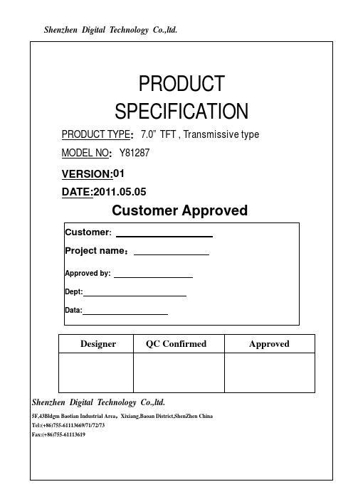
Shenzhen Digital Technology Co.,ltd.PRODUCTSPECIFICATIONPRODUCT TYPE:7.0” TFT , Transmissive typeMODEL NO:Y81287VERSION:01DATE:2011.05.05Customer ApprovedCustomer:Project name:Approved by:Dept:Data:Designer QC Confirmed ApprovedShenzhen Digital Technology Co.,ltd.5F,43Bldgm Baotian Industrial Area,Xixiang,Baoan District,ShenZhen ChinaTel:(+86)755-61113669/71/72/73Fax:(+86)755-61113619RECORDS OF REVISIONDESCRIPTIONS DATE Version REVISEDISSUE2011.05.05 01FIRST深圳市德智欣科技有限公司CONTENTS1. GENERAL DESCRIPTION - - - - - - - - - - - - - - - - - - - - - - - - - -2. MECHANICAL SPECIFICATIONS - - - - - - - - - - - - - - - - -- - - - - - - -3. OUTLINE DIMENSIONS - - - - - - - - - - - - - - - - - - - - -4. INTERFACE ASSIGNMENT - - - - - - - - - - - - - - - - - - - - - - - - --------5. TIMING CHARACTERISTICS - - - - - - - - - - - - - - - - - - - - - - - ------------------------------------------------6. RESETTIMINGCHARACTERISTICS7. POWER ON/OFF SEQUENCE - - - - - - - - - - - - - - - - - - - - - - - - - - -8. INSTRUCTION TABLE - - - - - - - - - - - - - - - - - - - - - - - - - - -9. ELECTRICAL CHARACTERISTICS - - - - - - - - - - - - - - - - - - - - -10. LED BACKLIGHT CHARACTERISTICS - - - - - - - - - - - - - - - - - - -11. OPTICAL CHARACTERISTICS - - - - - - - - - - - - - - - - - - - - - - - - - -Condition -----------------------------------------------------------12. Reliability13. Inspection Standards ----------------------------------------------------14. Precaution - - - - - - - - - - - - - - - - - - - - - - - -深圳市德智欣科技有限公司1.GENERAL DESCRIPTIONThis LCM Y81287 is a 800 x 3RGB x 480 dots matrix 7.0 ”TFT LCD module. It has a TFTpanel,composed of 1200 -channel source driver and 960-channel gate driver.2. MECHANICAL SPECIFICATIONSUNIT Item Contents LCD Type 7.0” TFT-LCD, TransmissiveOutline Dimension 100(W)x164.9(H)x3.4(T) mmActive Area 85.92(W) x151.68(H) mmViewing direction 6 O’CLOCK ---Source HX8664BDriver ICGate IC HX8264DDisplay Color 16MNumber of Dots 800(RGB)x480 DotsDot Pitch (H×V)0.0642(W) x 0.1790(H) mmAssy Type COG+FPC+BL ---BACKLIGHT WHITE LED Backlight -Interface24 bit interfaceWEIGHT TBD g深圳市德智欣科技有限公司4. INTERFACE ASSIGNMENTPIN NO. SYMBOL1 Power for LED backlighr (Anode) LEDA2 Power for LED backlighr (Anode) LEDA3 Power for LED backlighr (Cathode) LEDK4 Power for LED backlighr (Cathode) LEDKground GND5 Powervoltage VCOM6 Common7 Power for Digital Circuit DVDDmodeselect MODE8 DE/SYNC9 Data input Enable DE10 Vertical Sync Input VS11 Horizontal Sync Input HS12~19 Blue data B7~B020~27 Green data G7~G028~35 Red data R7~R036 Power ground GND37 Sample clock DCLK38 Power ground GND39 Left / right selection L/R40 Up/down selection U/D41 Gate NO Voltage VGH42 Gate OFF Voltage VGL43 Power for Analog Circuit A VDD44 Global reser pin RESET45 No connection NC46 Common Voltage VCOM47 Dithering function DITHB48 Power ground GND49 No connection NC50 No connection NC深圳市德智欣科技有限公司5.TIMING CHARACTERISTICS深圳市德智欣科技有限公司6.RESET TIMING CHARACTERISTICS深圳市德智欣科技有限公司7. POWER ON/OFF SEQUENCE深圳市德智欣科技有限公司8. HX8664B&HX8264D INSTRUCTION TABLE9. ELECTRICAL CHARACTERISTICS深圳市德智欣科技有限公司深圳市德智欣科技有限公司12. Reliability Condition13.Inspection Standards 13.1 Major DefectItem NoItems to be inspected Inspection Standard Classification of defects13.1.1 Allfunctional defects1)No display2) Display abnormally3) Missing vertical, horizontal segment 4) Short circuit5)Back-light no lighting flickering and abnormal lighting.13.1.2 Missing Missing component13.1.3 OutlinedimensionOverall outline dimension beyond the drawing is not allowed.Major13.2 Cosmetic defectItem No Item ConditionRemark1 High temperatureOperating 70°C ±2°C for 240 hours2 Low temperatureOperating -20°C ±2°C for 240 hours3 High temperatureStorage 80°C ±2°C for 240 hours4 Low temperatureStorage -30°C ±2°C for 240hours5High temperature & humidity Storage50℃±5°C , 90%RH, 120 hours 6Thermal Shock Storage (No operation)-20℃ , 30min.<=> 70℃ , 30min.10 Cycles7 ESD test-8 Vibration test 10 => 55 =>10 Hz, within 1 minute;Amplitude:1.5mm.15 minutes for each Direction ( X,Y ,Z ) 9 Drop testPacked, 100CM free fall6 sides, 1 corner, 3edgesNO DEFECT IN DISPLAYING AND OPERATIONAL FUNCTION深圳市德智欣科技有限公司(i) chips on cornerX Y Z ≤2.0≤SDisregardNotes:S=contact pad lengthChips on the corner of terminal shall not be allowed to extend intothe ITO pad or expose perimeter seal. Minor(ii)Usual surface cracksX Y Z≤3.0<Inner border line of the seal DisregardMinor13.3.1Glass defect(iii)CrackCracks tend to break are not allowed.Major13.3.2 Partsalignment1) Not allow IC and FPC/heat-seal lead width is more than 50 %beyond lead pattern.2) Not allow chip or solder component is off center more than 50 % of the pad outline. 13.3.3 SMTAccording to the <Acceptability of electronic assemblies>IPC-A-610C class 2 standard. Component missing or function defect are Major defect, the others are Minor defect.Major14. Precaution14.1 Handling(1) Protect the panel from static, it may cause damage to the CMOS Gate Array IC.(2) Use fingerstalls with soft gloves in order to keep display clean during the incominginspection and assembly process.(3) If the liquid crystal material leaks from the panel, it should be kept away from theeyes or mouth. In case of contact with hands, legs or clothes, it must be washedaway thoroughly with soap.(4) The desirable cleaners are water, IPA (Isopropyl Alcohol) or Hexane. Don’t useKetone type materials (ex. Acetone), Ethyl alcohol, Toluene, Ethyl acid or Methylchloride. It might permanent damage to the polarizer due to chemical reaction.(5) Pins of I/F connector shall not be touched directly with bare hands.(6) Refrain from strong mechanical shock and / or any force to the panel. In addition todamage, this may cause improper operation or damage to the panel.(7) Note that polarizers are very fragile and could be easily damaged. Do not press orscratch the surface harder than a B pencil lead.(8) Wipe off water droplets or oil immediately. If you leave the droplets for a long time,staining and discoloration may occur.(9) If the surface of the polarizer is dirty, clean it using some absorbent cotton or soft cloth.14.2 Storage(1) Do not leave the panel in high temperature, and high humidity for a long time. It ishighly recommended to store the panel with temperature from 0 to 35℃ andrelative humidity of less than 70%.(2) The panel shall be stored in a dark place. It is prohibited to apply sunlight orfluorescent light during the store.14.3 Operation(1) The LCD shall be operated within the limits specified. Operation at values outside ofthese limits may shorten life, and/or harm display images.(2) Do not exceed the absolute maximum rating value. (the supply voltage variation,Input voltage variation in part contents and environmental temperature and so on).Otherwise the panel may be damaged.(3) If the panel displays the same pattern continuously for a long period of time, it canbe the situation when the image” Sticks” to the screen.深圳市德智欣科技有限公司。
7寸LVDS TM070NA-01D(40PIN)
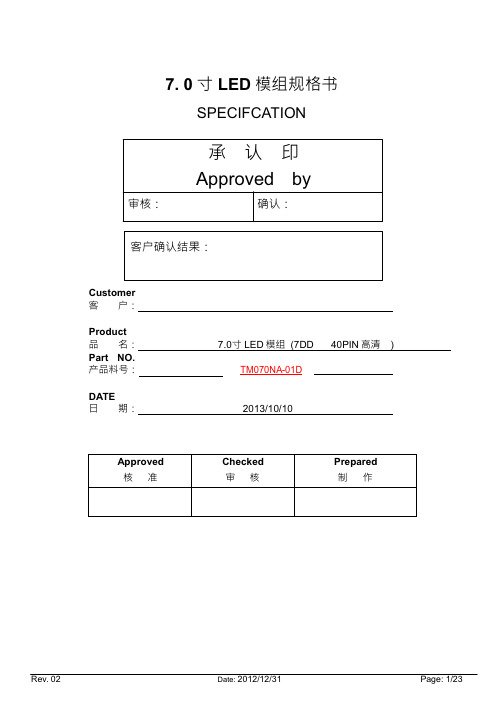
7.0⯟LED㨈享妫㠣ṍSPECIFCATION㉦宋⍗Approved by⮈㠟Ɲ䡕宋Ɲ⮉㈞䡕宋人㞃ƝCustomer⮉㈞ƝProduct⒨⏴Ɲ7.0⯟LED㨈享(7DD40PIN檿㷬) Part NO.Ẏ⒨㖀⏞ƝTM070NA-01DDATE㗌㜆Ɲ2013/10/10Approved 㠟↭Checked⮈㠟Prepared∝ὃContentsNO.Contents Page ---Cover1 ---Contents2 ---Document Revision History3 General Description4ṳAbsolute Maximum Ratings5 Optical Characteristics6⛂Block Diagram9ṻInterface Pin Connection10⅔Electrical Characteristics11 Reliability Test Items16⅒Outline Dimension17ṄPacking Form18⌨General Precaution20Document Revision HistoryChange No.Date Subject And Reason Version No.Responser 12012.12.31New011.0General Description1.1IntroductionTM070NA-01D is a color active matrix thin film transistor (TFT) liquid crystal display (LCD) that uses amorphous silicon TFT as a switching device.This model is composed of a TFT LCD panel and a driving circuit.This TFT LCD has a 7.0 (16:9) inch diagonally measured active display area with (1024 horizontal by600 vertical pixe l) resolution.1.2. Features7 (16:9 diagonal) inch configurationCompatible with NTSC & PAL systemImage Reversion: UP/DOWN and LEFT/RIGHTROHS design1.3. General informationItem Specification UnitOutline Dimension165.8 (H) x 105.4. (V) x2.8 (D) mmDisplay area153.6 (H) x 90 (V) mmNumber of Pixel1024RGB(H)x600(V)pixelsPixel pitch0.15(H)x0.15(V)s mmPixel arrangement RGB Vertical stripeDisplay mode Normally whiteColor Filter Array RGB vertical stripesBacklight White LEDWeight TBD g2.1Electrical Absolute Rating2.1.1TFT LCD ModuleItem Symbol Min.Max.Unit NotePower supply voltageV DD-0.3 5.0V GND=0 AV DD 6.513.5V AGND=0 VGH-0.342V GND=0 VGL-200.3V GND=0 V COM 2.7 4.7VAnalog Signal Input Level V R,V G,V B-0.2AV DD+0.2VLogic Signal Input Level V I-0.3 5.0VNote(1)Stresses above those listed under"Absolute Maximum Rating"may cause permanent damage to the device.These are stress ratings only.Functional operation of this device at indicated in the operational sections(6.1) of this specification.Item Symbol Min.Max.Unit Note Operating Temperature Topa-1060濎Storage Temperature Tstg-2070濎2.3Back-light Unit:PARAMETER Sym.Min.Typ.Max.Unit Test Condition NoteLED Current IF±140±mA±±LED Voltage VF99.910.5V±±Life Time±25000±Hr.I 180mA±Color WhiteNote(1)Permanent damage may occur to the LCD module if beyond this specification.Functional operation should be restricted to the conditions described under normal operating conditions.(2)Ta=25±2濎(3)Test condition:LED Current140mA3.0Optical Characteristics3.1Optical specification200250405050603.2Measuring ConditionŶMeasuring surrounding:dark roomŶAmbient temperature:25±2濎Ŷ30min.warm-up time.3.3Measuring EquipmentŶTOPCON BM-7ŶMeasuring spot size:field2°Note(1)Definition of Vsat and Vth (at20濎)Note(2)Definition of Viewing Angle:Note(3)Definition of Contrast Ratio(CR):measured at the center point of panelLuminance with all pixels whiteCR=Luminance with all pixels black Note(4)Definition of Response Time:Sum of T R and T F4.2Relationship Between Displayed Color and input5.0Interface Pin Connection 5.1TFT LCD Module6.1TFT LCD ModuleItemSymbol Min.Typ.Max.UnitNoteSupply VoltageV dd3.0 3.3 3.6V V GH 19.72020.3V V GL -6.5-6.8-7.1V AV DD10.81111.2V Video signal amplitude (VR,VG,VB)V IA --AV DD ±0.4V V IAC ---V AC component,V IDC -AV DD /2-V DC component VCOM V CAC --VP-P AC component V CDC 2.7 3.7 4.7V DC component,(1)Input signal voltageV IH 0.7DV DD-DV DD V (2)V IL 0-0.3DV DDV (2)Current of powersupplyI DD-25mA V CC =3.3V I ADD -35mA AV DD =11V I GH-0.45mAV GH =20V I GL -0.85mA V GL =6.8VNote (1):The brightness of LCD panel could be changed by adjusting the AC component of VCOM.Note (2):STHL,STHR,OEH,L/R,CPH1~CPH3,STVD,STVU,OEV,CKV,U/D6.3Input Clock and Data Timing Diaguam6.5Timing6.4Data Input Format7.0Reliability test itemsNO Item Conditions Remark 1High Temperature Storage Ta=+70濎,240hrs2Low Temperature Storage Ta=-20濎,240hrs3High Temperature Operation Ta=+60濎,240hrs4Low Temperature Operation Ta=-10濎,240hrs5High Temperature and HighHumidity(operation)Ta=+60濎,90%RH,240hrs6Thermal Cycling Test(nonoperation)-20濎(0.5hr)ĺ 70濎(0.5hr),200cycles7Vibration1.Random:1.04G,10-500HZ,X,Y,Zdirection30min/each direction2.Sweep sine:1.5G,5~500Hz,X/Y/Z,30min/each direction8Shock100G,6ms,±X,±Y,±Z3 time for each directionJIS C7021,A-10(Condition A)9Vibration(with carton)Random:1.04Grms,10~500Hz,X/Y/Z45min/each directionFixed:5Hz,1.5Grms,X/Y/Z45min/each direction10Drop(with carton)Height:60cm1corner,3edges,6surfaces JIS Z020211Electrostatic Discharge±200V,200PF,0ȍ time/each terminalNote:All tests above are practiced at module type.There is no display function NG issue occurred,All the cosmetic specification is judged before the reliability stress.TM070NA-01D9.0Packing form9.1Packing form16016110.0General Precaution10.1Use RestrictionThis product is not authorized for use in life supporting systems,aircraft navigation control systems,military systems and any other application where performance failure could be life-threatening or otherwise catastrophic.10.2Asembly Precaytton10.2.1Please use the mounting hole on the module side in installing and do not bending orwrenching LCD in assembling.And please do not drop,bend or twist LCD module inhandling.10.2.2Please design display housing in accordance with the following guide lines.10.2.2.1Housing case must be destined carefully so as not to put stresses on LCD allsides and not to wrench module.The stresses may cause non-uniformity even ifthere is no non-uniformity statically.10.2.2.2Keep sufficient clearance between LCD module back surface and housing whenthe LCD module is mounted.The clearance in the design is recommendedtaking into account the tolerance of LCD module thickness and mountingstructure height on the housing.10.2.3Please do not push or scratch LCD panel surface with any-thing hard.And do not soilLCD panel surface by touching with bare hands.(Polarizer film,surface of LCDpanel is easy to be flawed.)10.2.4Please do not press any parts on the rear side such as source IC,gate IC,and FPCduring handling LCD module.If pressing rear part is unavoidable,handle the LCDmodule with care not to damage them.10.2.5Please wipe out LCD panel surface with absorbent cotton or soft cloth in case of itbeing soiled.10.2.6Please wipe out drops of adhesives like saliva and water on LCD panel surfaceimmediately.They might damage to cause panel surface variation and color change.10.2.7Please do not take a LCD module to pieces and reconstruct it.Resolving andreconstructing modules may cause them not to work well.10.3Disassembling or ModificationDo not disassemble or modify the module.It may damage sensitive parts inside LCDmodule,and may cause scratches or dust on the display.HannStar does not warrant themodule,if customers disassemble or modify the module.10.4Breakage of LCD Panel10.4.1If LCD panel is broken and liquid crystal spills out,do not ingest or inhale liquidcrystal,and do not contact liquid crystal with skin.10.4.2If liquid crystal contacts mouth or eyes,rinse out with water immediately.10.4.3If liquid crystal contacts skin or cloths,wash it off immediately with alcohol and rinsethoroughly with water.10.4.4Handle carefully with chips of glass that may cause injury,when the glass is broken.TM070NA-01D10.5Absolute Maximum Ratings and Power Protection Circuit10.5.1Do not exceed the absolute maximum rating values,such as the supply voltagevariation,input voltage variation,variation in parts¶parameters,environmentaltemperature,etc.,otherwise LCD module may be damaged.10.5.2Please do not leave LCD module in the environment of high humidity and hightemperature for a long time.10.5.3It¶s recommended employing protection circuit for power supply.10.6Operation10.6.1Do not touch,push or rub the polarizer with anything harder than HB pencil efingerstalls of soft gloves in order to keep clean display quality,when persons handlethe LCD module for incoming inspection or assembly.10.6.2When the surface is dusty,please wipe gently with absorbent cotton or other softmaterial.10.6.3Wipe off saliva or water drops as soon as possible.If saliva or water drops contactwith polarizer for a long time,they may causes deformation or color fading.10.6.4When cleaning the adhesives,please use absorbent cotton wetted with a littlepetroleum benzine or other adequate solvent.10.7Static Electricity10.7.1Protection film must remove very slowly from the surface of LCD module to preventfrom electrostatic occurrence.10.7.2Because LCD module uses CMOS-IC on TFT-LCD panel,it is very weak toelectrostatic discharge.Please be careful with electrostatic discharge.10.7.3Persons who handle the module should be grounded through adequate methods.10.8DisposalWhen disposing LCD module,obey the local environmental regulations.10.9OTHERS10.9.1A strong incident light into LCD panel might cause display characteristics'changinginferior because of polarizer film,color filter,and other materials becoming inferior.Please do not expose LCD module direct sunlight land strong UV rays.10.9.2Please pay attention to a panel side of LCD module not to contact with othermaterials in preserving it alone.10.9.3For the packaging box,please pay attention to the followings:10.9.3.1Packaging box and inner case for LCD are designed to protect the LCDs fromthe damage or scratching during transportation.Please do not open exceptpicking LCDs up from the box.10.9.3.2Please do not pile them up more than6boxes.(They are not designed so.)Andplease do not turn over.10.9.3.3Please handle packaging box with care not to give them sudden shock andvibrations.And also please do not throw them up.10.9.3.4Packing box and inner case for LCDs are made of cardboard.So please payattention not to get them wet.(Such like keeping them in high humidity or wetplace can occur getting them wet.)。
群创7寸数字屏规格书
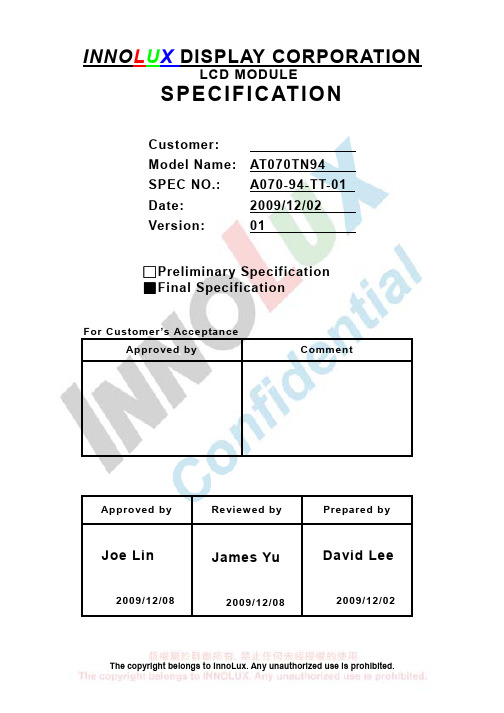
The copyright belongs to InnoLux. Any unauthorized use is prohibited.INNO L U X DISPLAY CORPORATIONLCD MODULESPECIFICATIONCustomer: Model Name: AT070TN94SPEC NO.: A070-94-TT-01 Date: 2009/12/02 Version:01□Preliminary Specification ■Final SpecificationFor Customer ’s AcceptanceApproved byCommentApproved byReviewed by Prepared byJoe Lin2009/12/08James Yu2009/12/08David Lee2009/12/02InnoLux copyright 2004All rights reserved,Copying forbidden.Record of RevisionVersion Revise Date Page ContentPre-Spec.01 2009/07/07 All Initial ReleaseFinal-spec.01 2009/12/02 All The first version final specification.6 Modify V COM to 3.8V(Typ.), 3.6V(Min.) and 4.0V(Max.).9 Add Input Clock and Data Timing Diagram.18 Update the Mechanical Drawing.The copyright belongs to InnoLux. Any unauthorized use is prohibited.I NNO L U XContents1. General Specifications (1)2. Pin Assignment (2)3. Operation Specifications (5)3.1. Absolute Maximum Ratings (5)3.1.1. Typical Operation Conditions (6)3.1.2. Current Consumption (7)3.1.3. Backlight Driving Conditions (7)3.2. Power Sequence (8)3.3. Timing Characteristics (9)3.3.1. AC Electrical Characteristics (9)3.3.2. Input Clock and Data Timing Diagram (9)3.3.3. Timing (10)3.3.4. Data Input Format (11)4. Optical Specifications (12)5. Reliability Test Items (16)6. General Precautions (17)6.1. Safety (17)6.2. Handling (17)6.3. Static Electricity (17)6.4. Storage (17)6.5. Cleaning (17)7. Mechanical Drawing (18)8. Package Drawing (19)8.1. Packaging Material Table (19)8.2. Packaging Quantity (19)8.3. Packaging Drawing (20)The copyright belongs to InnoLux. Any unauthorized use is prohibited.1. General SpecificationsNo. Item Specification Remark1 LCD size 7.0 inch(Diagonal)2 Driver element a-Si TFT active matrix3 Resolution 800 × 3(RGB) × 4804 Display mode Normally White, Transmissive5 Dot pitch 0.0642(W) × 0.1790(H) mm6 Active area 154.08(W) × 85.92(H) mm7 Module size 164.9(W) ×100.0(H) ×5.7(D) mm Note 18 Surface treatment Anti-Glare9 Color arrangement RGB-stripe10 Interface Digital11 Backlight power consumption 1.674W (Typ.)12 Panel power consumption 0.226W (Typ.)13 Weight 150g (Typ.)Note 1: Refer to Mechanical Drawing.2. Pin AssignmentFPC Connector is used for the module electronics interface. The recommended model is FH12A-50S-0.5SH manufactured by Hirose.Pin No. Symbol I/O Function Remark1 V LED+P Power for LED backlight (Anode)2 V LED+P Power for LED backlight (Anode)3 V LED-P Power for LED backlight (Cathode)4 V LED-P Power for LED backlight (Cathode)5 GND P Power ground6 V COM I Common voltage7 DV DD P Power for Digital Circuit8 MODE I DE/SYNC mode select Note 19 DE I Data Input Enable10 VS I Vertical Sync Input11 HS I Horizontal Sync Input12 B7 I Blue data(MSB)13 B6 I Blue data14 B5 I Blue data15 B4 I Blue data16 B3 I Blue data17 B2 I Blue data18 B1 I Blue data Note 219 B0 I Blue data(LSB) Note 220 G7 I Green data(MSB)21 G6 I Green data22 G5 I Green data23 G4 I Green data24 G3 I Green data25 G2 I Green data26 G1 I Green data Note 227 G0 I Green data(LSB) Note 228 R7 I Red data(MSB)29 R6 I Red data30 R5 I Red data31 R4 I Red data32 R3 I Red data33 R2 I Red data34 R1 I Red data Note 235 R0 I Red data(LSB) Note 236 GND P Power Ground37 DCLK I Sample clock Note 338 GND P Power Ground39 L/R I Left / right selection Note 4,540 U/D I Up/down selection Note 4,541 V GH P Gate ON Voltage42 V GL P Gate OFF Voltage43 AV DD P Power for Analog Circuit44 RESET I Global reset pin. Note 645 NC - No connection46 V COM I Common Voltage47 DITHB I Dithering function Note 748 GND P Power Ground49 NC - No connection50 NC - No connectionI: input, O: output, P: PowerNote 1: DE/SYNC mode select. Normally pull high.When select DE mode, MODE=”1”, VS and HS must pull high.When select SYNC mode,MODE= ”0”, DE must be grounded.Note 2: When input 18 bits RGB data, the two low bits of R,G and B data must be grounded.Note 3:Data shall be latched at the falling edge of DCLK.Note 4: Selection of scanning modeSetting of scan control inputU/D L/R Scanning direction GND DV DD Up to down, left to right DV DD GND Down to up, right to left GND GND Up to down, right to left DV DDDV DDDown to up, left to rightNote 5: Definition of scanning direction. Refer to the figure as below:Note 6: Global reset pin. Active low to enter reset state. Suggest to connect with an RCreset circuit for stability. Normally pull high.Note 7: Dithering function enable control, normally pull high. When DITHB=”1”,Disable internal dithering function, When DITHB=”0”,Enable internal dithering function,RightLeft DownUp3. Operation Specifications3.1. Absolute Maximum Ratings(Note 1)ValuesItem SymbolMin. Max.Unit RemarkDV DD -0.3 5.0 VAV DD 6.5 13.5 VV GH -0.3 40.0 VV GL -20.0 0.3 V Power voltageV GH-V GL- 40.0 V Operation Temperature T OP -30 85 ℃Storage Temperature T ST-30 85 ℃LED Reverse Voltage V R- 1.2 VEach LEDNote 2 LED Forward Current I F- 25 mA Each LEDNote 1: The absolute maximum rating values of this product are not allowed to be exceeded at any times. Should a module be used with any of the absolute maximum ratingsexceeded, the characteristics of the module may not be recovered, or in an extremecase, the module may be permanently destroyed.Note 2: V R Conditions: Zener Diode 20mA3.1.1. Typical Operation Conditions( Note 1)ValuesUnit Remark Item SymbolMin. Typ. Max.DV DD 3.0 3.3 3.6 V Note 2AV DD 10.2 10.4 10.6 VPower voltageV GH 15.3 16.0 16.7 VV GL -7.7 -7.0 -6.3 VInput signal voltage V COM 3.6 3.8 4.0 VInput logic high voltage V IH 0.7 DV DD - DV DD VNote 3 Input logic low voltage V IL 0 - 0.3 DV DD VNote 1: Be sure to apply DV DD and V GL to the LCD first, and then apply V GH.Note 2: DV DD setting should match the signals output voltage (refer to Note 3) of customer’s system board.Note 3: DCLK,HS,VS,RESET,U/D, L/R,DE,R0~R7,G0~G7,B0~B7,MODE,DITHB.3.1.2. Current ConsumptionValuesItem SymbolMin. Typ. Max.Unit RemarkI GH - 0.2 1.0 mA V GH =16.0VI GL - 0.2 1.0 mA V GL = -7.0V IDV DD - 4.0 10 mA DV DD =3.3VCurrent for DriverIAV DD - 20 50 mA AV DD =10.4V3.1.3. Backlight Driving ConditionsValuesItem SymbolMin. Typ. Max.Unit Remark Voltage for LED backlight V L 8.4 9.3 10.2 V Note 1 Current for LED backlight I L 170 180 200 mALED life time - 20,000 - - Hr Note 2Note 1: The LED Supply Voltage is defined by the number of LED at Ta=25℃ andI L =180mA.Note 2: The “LED life time” is defined as the module brightness decrease to 50% original brightness at Ta=25℃ and I L =180mA. The LED lifetime could be decreased ifoperating I L is lager than 180mA.3.2. Power Sequencea. Power on:Note: Data include R0~R7, B0~B7, GO~G7, U/D, L/R, DCLK, HS,VS,DE.DV DD→VGL→AVDD→VGH→Data→B/LB/L→Data→VGH→AVDD→VGL→DV DD3.3. Timing Characteristics3.3.1. AC Electrical CharacteristicsValuesItem SymbolMin. Typ. Max.Unit Remark HS setup time T hst8 - - nsHS hold time T hhd 8 - - nsVS setup time T vst8 - - nsVS hold time T vhd8 - - nsData setup time T dsu8 - - nsData hole time T dhd8 - - nsDE setup time T esu 8 - - nsDE hole time T ehd8 - - nsDV DD Power On Slew rate T POR - - 20 ms From 0 to 90% DV DDRESET pulse width T Rst 1 - - ms DCLK cycle time T coh 20 - - ns DCLK pulse duty T cwh 40 50 60 %3.3.2. Input Clock and Data Timing Diagram3.3.3. TimingValuesUnit Remark Item SymbolMin. Typ. Max.Horizontal Display Area thd- 800 - DCLKDCLK Frequency fclk26.4 33.3 46.8 MHzOne Horizontal Line th862 1056 1200 DCLKHS pulse width thpw 1 - 40 DCLKHS Blanking thb46 46 46 DCLKHS Front Porch thfp 16 210 354 DCLKValuesItem SymbolUnit RemarkMin. Typ. Max.Vertical Display Area tvd- 480 - THVS period time tv 510 525 650 THVS pulse width tvpw 1 - 20 THVS Blanking tvb23 23 23 THVS Front Porch tvfp7 22 147 TH3.3.4. Data Input Format4. Optical SpecificationsValuesItem Symbol ConditionMin. Typ. Max.Unit RemarkθL Φ=180°(9 o’clock) 60 70 -θRΦ=0°(3 o’clock) 60 70 -θTΦ=90°(12 o’clock) 40 50 -Viewing angle(CR≥ 10)θBΦ=270°(6 o’clock) 60 70 -degree Note 1T ON - 10 20 msec Note 3 Response timeT OFF - 15 30 msec Note 3 Contrast ratio CR 400 500 - - Note 4W X 0.26 0.31 0.36 -Color chromaticityW Y 0.28 0.33 0.38 -Note 2Note 5Note 6 Luminance L 320 400 - cd/m² Note 6 LuminanceuniformityY UNormalθ=Φ=0°70 75 - % Note 7Test Conditions:1. DV DD=3.3V, I L=180mA (Backlight current), the ambient temperature is 25℃.2. The test systems refer to Note 2.Note 1: Definition of viewing angle rangeFig. 4-1 Definition of viewing angleNote 2: Definition of optical measurement system.The optical characteristics should be measured in dark room. After 30 minutesoperation, the optical properties are measured at the center point of the LCD screen. (Response time is measured by Photo detector TOPCON BM-7, other items are measured by BM-5A/Field of view: 1° /Height: 500mm.)Normal line θ=Φ=0°Photo detectorΦ=90°12 o’clock directionΦ=270° 6 o’clock directionΦ=0°Φ=180°Active Area500mmLCMNormal line θ=Φ=0°Φ=90°12 o’clock directionΦ=270°6 o’clock directionΦ=0°Φ=180°Active AreaθLθTθBθRLCMNote 3: Definition of Response timeThe response time is defined as the LCD optical switching time interval between“White” state and “Black” state. Rise time (T ON) is the time between photo detector output intensity changed from 90% to 10%. And fall time (T OFF) is the timebetween photo detector output intensity changed from 10% to 90%.Fig. 4-3 Definition of response timeNote 4: Definition of contrast ratiostateBlack""theonLCDwhenmeasuredLuminancestateWhite""theonLCDwhenmeasuredLuminance(CR)ratioContrast=Note 5: Definition of color chromaticity (CIE1931)Color coordinates measured at center point of LCD.Note 6: All input terminals LCD panel must be ground while measuring the center area of the panel.The LED driving condition is I L=180mA .90%10%0%Photodetectoroutput(Relativevalue)ONTWhite (TFT OFF) Black (TFT ON) White (TFT OFF)Note 7:Definition of Luminance UniformityActive area is divided into 9 measuring areas (Refer to Fig. 4-4 ).Every measuring point is placed at the center of each measuring area.maxminBB(Yu)UniformityLuminance=L-------Active area length W----- Active area widthWW/3W/3W/6L/3L/3L/6LFig. 4-4 Definition of measuring pointsB max: The measured maximum luminance of all measurement position.B min: The measured minimum luminance of all measurement position.5. Reliability Test Items(Note3)Item Test Conditions Remark High Temperature Storage Ta = 85℃240hrs Note 1,Note 4 Low Temperature Storage Ta = -30℃240hrs Note 1,Note 4 High Temperature Operation Ts = 85℃240hrs Note 2,Note 4 Low Temperature Operation Ta = -30℃240hrs Note 1,Note 4 Operate at High Temperatureand Humidity+60℃, 90%RH 240hrs Note 4Thermal Shock -30℃/30 min ~ +85℃/30 min for a total 100cycles, Start with cold temperature and endwith high temperature.Note 4Vibration Test Frequency range:10~55Hz Stroke:1.5mmSweep:10Hz~55Hz~10Hz2 hours for each direction of X. Y. Z.(6 hours for total)Mechanical Shock 100G 6ms,±X, ±Y, ±Z 3 times for each directionPackage Vibration Test Random Vibration :0.015G*G/Hz from 5-200HZ, -6dB/Octave from 200-500HZ2 hours for each direction of X. Y. Z.(6 hours for total)Package Drop Test Height:60 cm1 corner, 3 edges, 6 surfacesElectro Static Discharge ± 2KV, Human Body Mode, 100pF/1500ΩNote 1: Ta is the ambient temperature of samples.Note 2: Ts is the temperature of panel’s surface.Note 3: In the standard condition, there shall be no practical problem that may affect the display function. After the reliability test, the product only guarantees operation,but don’t guarantee all of the cosmetic specification.Note 4: Before cosmetic and function test, the product must have enough recovery time, at least 2 hours at room temperature.6. General Precautions6.1. SafetyLiquid crystal is poisonous. Do not put it in your mouth. If liquid crystal touches your skin or clothes, wash it off immediately by using soap and water.6.2. Handling1. The LCD panel is plate glass. Do not subject the panel to mechanical shock or toexcessive force on its surface.2. The polarizer attached to the display is easily damaged. Please handle it carefullyto avoid scratch or other damages.3. To avoid contamination on the display surface, do not touch the module surfacewith bare hands.4. Keep a space so that the LCD panels do not touch other components.5. Put cover board such as acrylic board on the surface of LCD panel to protect panelfrom damages.6. Transparent electrodes may be disconnected if you use the LCD panel underenvironmental conditions where the condensation of dew occurs.7. Do not leave module in direct sunlight to avoid malfunction of the ICs.6.3. Static Electricity1. Be sure to ground module before turning on power or operating module.2. Do not apply voltage which exceeds the absolute maximum rating value.6.4. Storage1. Store the module in a dark room where must keep at 25±10℃ and 65%RH or less.2. Do not store the module in surroundings containing organic solvent or corrosivegas.3. Store the module in an anti-electrostatic container or bag.6.5. Cleaning1. Do not wipe the polarizer with dry cloth. It might cause scratch.2. Only use a soft sloth with IPA to wipe the polarizer, other chemicals mightpermanent damage to the polarizer.7. Mechanical Drawing8. Package Drawing8.1. Packaging Material TableNo. ItemModel(Material)Dimensions(mm)UnitWeight(kg)Quantity Remark1 LCMModuleAT070TN94 164.9 × 100.0 × 5.7 0.150 50pcs2 Partition BC Corrugatedpaper512 × 349 × 226 1.466 1set3 CorrugatedPaperB Corrugatedpaper510 × 350 0.071 4pcs4 CorrugatedBarB Corrugatedpaper512 × 11 × 3 0.046 4pcs5 Dust-ProofBagPE 700 × 530 0.048 1pcs6 A/S Bag PE 180 × 133 × 0.2 0.002 50pcs7 Carton Corrugatedpaper530 × 355 × 255 1.100 1pcs8 Total weight 10.682 kg± 5%8.2. Packaging QuantityTotal LCM quantity in Carton: no. of Partition 2 Rows × quantity per Row 25 = 508.3. Packaging Drawing。
AT070MJ01_三菱7寸宽温1000nits-杭州旭虹科技有限公司
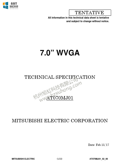
7.0” WVGA
TECHNICAL SPECIFICATION AT070MJ01
MITSUBISHI ELECTRIC CORPORATION
Date: Feb.15,’17
MITSUBISHI ELECTRIC
(1/25)
AT070MJ01_02_00
Global LCD Panel Exchange Center
工业液晶屏:http://www.hzxuhong.com
TENTATIVE
All information in this technical data sheet is tentative and subject to change without notice.
MITSUBISHI’s TFT-LCD module is designed and produced for “General Application” which is described as below.
<General Application> Computers, office automation equipment, factory automation equipment, test and measurement equipment, communications, medical equipment which has no impact for human life and body, display equipment utilized in transportation system (automobiles, ships, trains, etc) which has no influence on its operation directly or indirectly.
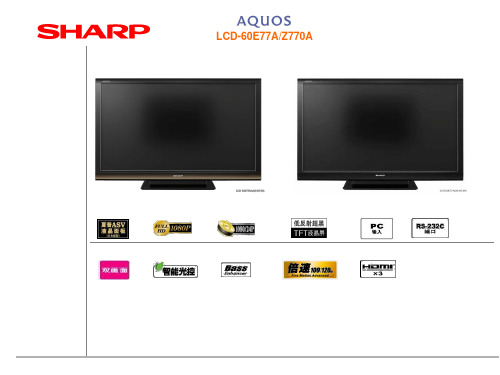
夏普LCD-60Z770A液晶彩电培训教材
6.点击START
设置完成后点击Start按钮.开始升级,约5秒后出现如下,点击确定 即可
当看到ISP SUCCES即表示升级成功.
谢谢各位!
无电源(指示灯不亮)或无法启动(指示灯不能从红色转为绿色) N
P2801(11)脚BU+5V是否正常
更换电源板单元 检查AC_CTRL和PNL_ON信号线
Y
P2801(10)脚AC_CTRL 、(12)脚PNL_ON控制信号是否正常
N
Y
P2801(1)、(2)、(3)、(4)脚13.5V是否正常
N
Sequoia
LVDS
INV_STB/INV_OFL
RESET IC2006 XTAL 16MHz
T-CON
INVERTER
EEPROM IC2009
BU+5V UR +15V PS_ON
XTAL X801 19.66MHz
60V
220V
POWER UNIT
AC_DET
AUDIO AMP IC1301
DDR ROM
DDR ROM
LCD-60E77A/Z770A单元电路 详见电路图分析
IC2001 MCU IXC182WJ
HP_DET 耳机检测
AC_DET IN
POW OUT
AC_DET OUT TO Sequoia
LAMP ERR 灯保护
KEY_POW
IR_IN RS-232 RX/TX
RESET IN PC_V/H IN
检查IC801及其外围电路
Y
是否有I2S信号从IC801的34、119、196、266脚输出?
N
检查IC801及其外围电路
Philips 170X5 17 英寸 LCD 显示器说明书
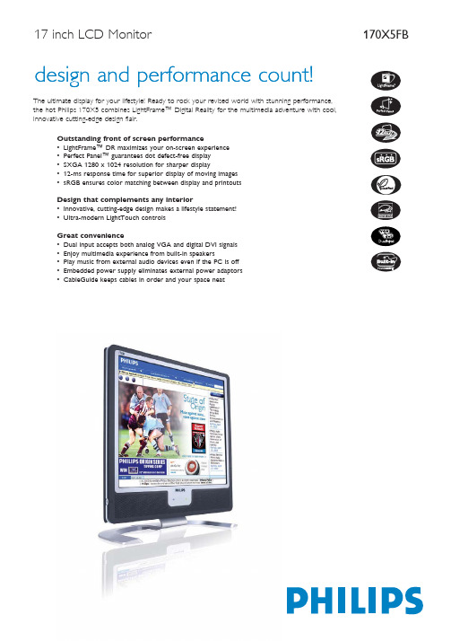
17 inch LCD MonitorPicture/ DisplayCommercial Specifications•LCD panel type 1280 x 1024 pixels,Anti-glare polarizer,RGB Vertical stripe •Panel size 17"/ 43 cm•Effective viewing area 337.9 x 270.3 mm •Pixel pitch 0.264 x 0.264 mm •Brightness (nits) 250•Contrast ratio 500:1•Display colors 16.2 M•Viewing angle (C/R > 5) - Horizontal : 160°- Vertical : 160°• Response time 12 ms• White chromaticity, 6500º K x = 0.313 / y = 0.329• White chromaticity, 9300º K x = 0.283 / y = 0.297• Maximum resolution 1280 x 1024 @ 75Hz • Recommended resolution 1280 x 1024 @ 60Hz • Factory preset modes 16 modes• User definable modes 16 modes• Video dot rate 140 MHz• Horizontal scanning frequency 30 - 83 KHz• Vertical scanning frequency 56 - 76 Hz• Picture enhancement LightFrame™ digitalreality• sRGB YesConnectivity• Signal input Analog (VGA), DVI-D,PC Audio in• I/O interface on pad Headphone jack• Video sync input signal Sync on green,Separate sync,Composite sync Convenience• Built-in audio 2 W RMS x 2 stereospeakers• Buttons and controls LightTouch controls,Customized hot key,Side keys• Convenience enhancements On-screen DisplaySmartControl• Monitor controls Auto, Brightness control,Left/Right, LightFrame,Menu (OK), Power On/Off,Up/Down, Volume control • OSD languages English, French, German,Italian, Simplified Chinese,Spanish• Other convenience features Kensington lock compatible • Plug & Play compatibility DDC/CI, sRGB,Windows 98/ME/2000/XP • Regulatory approvals CE Mark, E2000, FCC-B,UL, CSA, MPR-II,Low Emission,Energy Star, SEMKO,TÜV/GS, TÜV Ergo• Tilt -5° to 25°LightFrame™ Digital RealityLightFrame™ Digital Reality is an integrated software and hardware solution for Philips high-end monitors that delivers high quality visual display enhancements to users through quick and convenient hardware or software interfaces.Perfect Panel™Bright dots and dark dots are defects in a LCD panel. While some manufacturers still consider bright and dark defects in an LCD panel an inevitable part of the manufacturing process, Philips doesn't. Philips monitors are produced with zero tolerance for LCD panel defects and backed by our Perfect Panel™ guarantee providing repair or replacement of any LCD monitor that displays even a single defective bright or dark dot.SXGA, 1280 x 1024 resolutionFor graphics monitors, the screen resolution signifies the number of dots (pixels) on the entire screen. For example, a1280-by-1024 pixel screen is capable of displaying 1280 distinct dots on each of 1024 lines, or about 1.3 million pixels.12-ms response timeResponse time is the period required for a liquid crystal cell to go from active (black) to inactive (white) and back to active (black) again. It is measured in milliseconds. Faster is better: Lower response time means faster transitions and, therefore, results in fewer visible image artifacts in the display of fast-moving images. sRGB readyCalibrated RGB that is optimized for the vast majority of computer peripherals, monitors, operating systems and browsers, allowing accurate color mapping with very little data overhead. Innovative cutting-edge designAn exclusive design concept that combines smooth, flowing lines reminiscent fine modern sculpture with ultra modern materials and techno touches to create a monitor that makes a lifestyle statement.LightTouch controlsUltra-responsive, touch sensitive icons that replace protruding buttons. Responding to your lightest touch, LightTouch controls,for example, power up your monitor or brighten and sharpen your display with LightFrame™. When activated, LightTouch icons glow to indicate that your commands have been implemented.Dual inputDual input provides connectors to accommodate input of both analog VGA and digital DVI signals.Built-in SpeakersAudio speakers built into a display device.Stand-alone audio functionBuilt-in advanced firmware that delivers audio output from external audio devices including a portable tape, CD or MP3 player even when there is no video input.Embedded power supplyAn embedded power supply is a power adaptor built into the body of a display device that replaces a bulky external power adaptor.CableGuideA convenient set of cable guides built into the rear of Philips monitors that keeps cables untangled and organized cables, helping you maintain a tidy, well ordered space.Product HighlightsAccessories• Included accessories AC Power cord,Audio cable,VGA cable• User manual Yes Dimensions• Depth (with base) 181.4 mm• Height (with base) 400 mm• Width (with base) 388.2 mm• MTBF 50,000 hrs• Relative humidity 20 % - 80 %• Temperature range (Operation) 5°C to 35°C• Temperature range (Storage) -20°C to 60°C• Weight 5.5 kgPower• Complies with E2000, Energy Star,NUTEK• Consumption 35 W (Typical)• Off mode <1 W• Power LED indicator Operation, green;Stand by/Sleep,amber• Power supply Built-in, 90-264 VAC,50/60 Hz Trademarks owned by Royal Philips Electronics2004 © Royal Philips Electronics - All rights reserved As an Energy Star partner, Philips has determined that this product meets the Energy Star guidelines for energy efficiency.Microsoft and Windows are registered trademarks of Microsoft Corporation.All data subject to change without noticeRelease date: January 2005, v.2。
新希液显示7寸HDMI TFT用户指南说明书
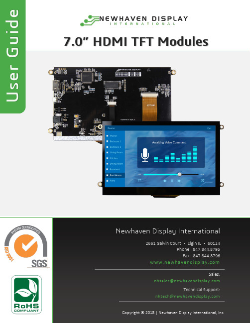
7.0” HDMI TFT ModulesNewhaven Display International2661 Galvin Court ▪ Elgin IL ▪ 60124Phone: 847.844.8795 Fax: 847.844.8796Sales:*************************** Technical Support:**************************U s e r G u i d ePart NumberingNHD - x.x - HDMI - N - xxxx - xxx1 2 3 4 5 61 Manufacturer –Newhaven Display2 Size (in inches)–5.0” Diagonal–7.0” Diagonal3 Interface –HDMI Interface4 Descriptor –800x480 Resolution, Video Only [HDMI audionot supported]5 Type–Standard–Premium MVA [Higher Brightness, Extended Viewing Angles]–Sunlight Readable6 Touch Panel–No Touch–Capacitive USB-HID [Pre-calibrated, No external drivers needed]–Resistive USB-HID [Pre-calibrated, No external drivers needed]Table of ContentsOverview (3)Functions and Features (3)Model Information (4)Electrical Characteristics (4)HDMI Receiver Information (4)Interface Description (5)Connecting with Windows/Windows Embedded (6)Connecting with Linux (8)Technical Resources (9)2D Drawings (9)3D Models (9)EDID Timing (9)Schematic (9)EDID Array (9)Quality Information (10)Precautions for Using LCDs/LCMs (10)Warranty Information (10)Document Revision History (11)OverviewThe HDMI interface has become the most popular video interface standard to date, and HDMI video sources are easier to come by now than ever before. Whether you need an HDMI TFT display for your Raspberry Pi/BeagleBone Black application, a Windows/Windows Embedded PC monitor, or a touch screen HMI for your Linux or other embedded system, the Newhaven Display HDMI TFT product line offers a solution.Our HDMI TFT Modules unite our existing high-quality TFT display panels with a custom PCB engineered in the USA by Newhaven Display. Assembled to the display, our PCB provides the user an all-in-one, plug-and-play HDMI + USB Touch solution for virtually any application.Functions and Features7.0” HDMI TFT Module w/ USB-HID Capacitive or Resistive Touch optionsOn-board Texas Instruments TFP401A HDMI/DVI ReceiverHDMI (Type-A) InputCompatible with PC (Windows/Linux)Compatible with Linux based SBCs such as Raspberry Pi, BeagleBone, etc.Plug-and-play USB-HID Touch, no external driver installation required24-bit True Color, 800x480 Resolution (WVGA)On-board Texas Instruments TPS61165 High Brightness LED Driver w/ PWMStandard, Premium MVA, and Sunlight Readable options available4 x 3.5mm Mounting Holes Enabling Standard M3 or #6-32 ScrewsOpen-Source Hardware, Engineered in Elgin, IL (USA)Model InformationHDMI Module P/N TFT Panel Used Display Type Luminance Rating Optimal Viewing Angle Touch PanelNHD-7.0-HDMI-N-RTXL NHD-7.0-800480EF-ATXL# Standard 280 cd/m² 12:00 No Touch NHD-7.0-HDMI-N-RSXV NHD-7.0-800480EF-ASXV# Premium MVA 800 cd/m² 75° all angles NHD-7.0-HDMI-N-RSXN NHD-7.0-800480EF-ASXN# Sunlight Readable 1000 cd/m² 12:00 NHD-7.0-HDMI-N-RTXL-CTU NHD-7.0-800480EF-ATXL#-CTP Standard 230 cd/m² 12:00 Projected Capacitive (USB-HID) NHD-7.0-HDMI-N-RSXV-CTU NHD-7.0-800480EF-ASXV#-CTP Premium MVA 660 cd/m² 75° all angles NHD-7.0-HDMI-N-RSXN-CTU NHD-7.0-800480EF-ASXN#-CTP Sunlight Readable 830 cd/m² 12:00 NHD-7.0-HDMI-N-RTXL-RTUNHD-7.0-800480EF-ATXL#-TStandard220 cd/m²6:004-WireResistive(USB-HID)NHD-7.0-HDMI-N-RSXV-RTU NHD-7.0-800480EF-ASXV#-T PremiumMVA600 cd/m² 75° all angles NHD-7.0-HDMI-N-RSXN-RTU NHD-7.0-800480EF-ASXN#-T SunlightReadable780 cd/m² 6:00For detailed information on the TFT Panel used, please view its Product Specification by accessing the product webpage link above.Electrical CharacteristicsItemSymbol ConditionMin.TypicalMax. Unit Operating Temperature Range T OP Absolute Max -20 - +70 ⁰C Storage Temperature Range T STAbsolute Max -30- +80 ⁰C Backlight PWM Frequency f PWM- 5 - 100 kHz Module Supply Voltage V DD- 5.0 - 7.5 V Standard models (RTXL)Module Supply CurrentI DDV DD = 5V -550 580 mA V DD = 7.5V -360 390 mA Premium MVA / Sunlight Readable models (RSXV, RSXN)Module Supply CurrentI DDV DD = 5V -750 790 mA V DD = 7.5V -560590mAHDMI Receiver InformationOn-board Texas Instruments TFP401A Receiver.To view the full TFP401A specification, please download it by accessing the link below: /lit/ds/slds190a/slds190a.pdfInterface Description(Capacitive Touch model shown above as reference)Num. Description1) (LED2)LED Indicator for Touch–Resistive Touch models onlyThis is a Red LED that will blink slowly (once per second) if the RTP controller is powered ON, awake, and no touch isdetected. This LED will blink rapidly (5 times per second) if the RTP controller detects a touch.2) (LED4)LED Indicator for Touch–Capacitive Touch models onlyThis is a Red LED that will illuminate when there is a touch sensed on the CTP.3) (LED3)LED Indicator for PowerThis is a Green LED that will illuminate when DC power is supplied to the module.4) (CN3)DC Jack (Center-Positive)This is used to supply power to the display module. A DC power supply in the range of 5V – 7.5V must be used.The output current rating of the DC power supply should be at least the maximum Supply Current (I DD) listed in the Electrical Characteristics section on the previous page.5) (CN4)Surface Mount Pin Header, 2.54mm pitch, for Backlight PWMThe pin labelled ‘PWM’ is connected directly to the LED driver’s CTRL pin (T.I. TPS61165). This is a multifunctional pin whi ch can be used for enable control, PWM, and digital dimming. A PWM frequency in the range of 5kHz – 100kHz must be used.6) (CN2)Micro-USB (Type-B) Connector for Touch–Touch Panel models onlyThis is to connect the Touch Panel of this module to a USB input to act as a USB-HID device.7) (LED1)LED Indicator for VideoThis is a Blue LED that will illuminate when there is an active video signal detected.8) (CN1)HDMI (Type-A) ConnectorThis is a full-size HDMI connector meant to connect the HDMI source signal (Video only) to this module.The on-board T.I. TFP401A HDMI/DVI Receiver does not scale video resolutions. Therefore, the output resolution of thesource must be 800x480 (WVGA). In most applications, this is automatically detected by the HDMI source.Connecting with Windows/Windows EmbeddedConnecting our HDMI TFT Modules to a Windows system is fully plug-and-play. Start by plugging in a DC power supply in the range of 5 - 7.5V, with at least 1A of output current. The green LED near the DC jack will illuminate when the board has power supplied to it. Next, connect the display to your system via HDMI cable. Due to the on-board EDID, the display will be detected automatically and the system’s output resolution will set itself to 800x480.For Touch Panel models, once the display is connected to the system via USB, Windows willautomatically detect and install the necessary drivers.The above window is shown for the Capacitive Touch model. The Resistive Touch model will also install automatically, however it will be labelled ‘AR1100 HID-MOUSE’ instead of ‘Newhaven Display’.Once Windows has finished installing the drivers, the device will show as ‘Ready to use’.For reference, in Device Manager the USB-HID Touch device will show as below:Connecting with LinuxMost Linux applications with an HDMI source will also be fully plug-and-play, however when using our HDMI TFT Modules with the Raspberry Pi, the config.txt file on the Pi’s microSD card will need to beslightly modified by the user.The following highlighted lines need to be added in config.txt for proper display output:# For more options and information see# http://rpf.io/configtxt# Some settings may impact device functionality. See link above for details# uncomment if you get no picture on HDMI for a default "safe" mode#hdmi_safe=1# uncomment this if your display has a black border of unused pixels visible# and your display can output without overscan#disable_overscan=1# uncomment the following to adjust overscan. Use positive numbers if console# goes off screen, and negative if there is too much border#overscan_left=16#overscan_right=16#overscan_top=16#overscan_bottom=16# uncomment to force a console size. By default it will be display's size minus# overscan.#framebuffer_width=1280#framebuffer_height=720# uncomment if hdmi display is not detected and composite is being output#hdmi_force_hotplug=1# uncomment to force a specific HDMI mode (this will force VGA)#hdmi_group=1#hdmi_mode=1hdmi_group=2hdmi_mode=87hdmi_cvt=800 480 60 6 0 0 0# uncomment to force a HDMI mode rather than DVI. This can make audio work in# DMT (computer monitor) modes#hdmi_drive=2# uncomment to increase signal to HDMI, if you have interference, blanking, or# no display#config_hdmi_boost=4# uncomment for composite PAL#sdtv_mode=2#uncomment to overclock the arm. 700 MHz is the default.#arm_freq=800# Uncomment some or all of these to enable the optional hardware interfaces#dtparam=i2c_arm=on#dtparam=i2s=on#dtparam=spi=on# Uncomment this to enable the lirc-rpi module#dtoverlay=lirc-rpi# Additional overlays and parameters are documented /boot/overlays/README# Enable audio (loads snd_bcm2835)dtparam=audio=onTechnical Resources2D DrawingsNHD-7.0-HDMI-N-RTXL NHD-7.0-HDMI-N-RSXV NHD-7.0-HDMI-N-RSXN NHD-7.0-HDMI-N-RTXL-CTU NHD-7.0-HDMI-N-RSXV-CTU NHD-7.0-HDMI-N-RSXN-CTU NHD-7.0-HDMI-N-RTXL-RTU NHD-7.0-HDMI-N-RSXV-RTU NHD-7.0-HDMI-N-RSXN-RTU 3D ModelsNHD-7.0-HDMI-N-xxxx NHD-7.0-HDMI-N-xxxx-CTU NHD-7.0-HDMI-N-xxxx-RTUEDID TimingSchematicNHD-7.0-HDMI-NEDID Arrayconst unsigned char NHD_HDMI7[] = {0x00, 0xFF, 0xFF, 0xFF, 0xFF, 0xFF, 0xFF, 0x00, 0x39, 0x04, 0x4F, 0x07, 0x00, 0x00, 0x00, 0x00,0x01, 0x11, 0x01, 0x03, 0x80, 0x0F, 0x09, 0x00, 0x0A, 0x00, 0x00, 0x00, 0x00, 0x00, 0x00, 0x00, 0x00, 0x00, 0x00, 0x00, 0x00, 0x00, 0x01, 0x01, 0x01, 0x01, 0x01, 0x01, 0x01, 0x01, 0x01, 0x01, 0x01, 0x01, 0x01, 0x01, 0x01, 0x01, 0x80, 0x0C, 0x20, 0x80, 0x30, 0xE0, 0x2D, 0x10, 0x28, 0x30, 0xD3, 0x00, 0x9A, 0x56, 0x00, 0x00, 0x00, 0x18, 0x00, 0x00, 0x00, 0xFC, 0x00, 0x4E, 0x48, 0x44, 0x2D, 0x37, 0x2E, 0x30, 0x20, 0x48, 0x44, 0x4D, 0x49, 0x0A, 0x00, 0x00, 0x00, 0x10, 0x00, 0x00, 0x00, 0x00, 0x00, 0x00, 0x00, 0x00, 0x00, 0x00, 0x00, 0x00, 0x00, 0x00, 0x00, 0x00, 0x00, 0x10, 0x00, 0x00, 0x00, 0x00, 0x00, 0x00, 0x00, 0x00, 0x00, 0x00, 0x00, 0x00, 0x00, 0x00, 0x00, 0xFB, 0x00, 0x00, 0x00, 0x00, 0x00, 0x00, 0x00, 0x00, 0x00, 0x00, 0x00, 0x00, 0x00, 0x00, 0x00, 0x00, 0x00, 0x00, 0x00, 0x00, 0x00, 0x00, 0x00, 0x00, 0x00, 0x00, 0x00, 0x00, 0x00, 0x00, 0x00, 0x00, 0x00, 0x00, 0x00, 0x00, 0x00, 0x00, 0x00, 0x00, 0x00, 0x00, 0x00, 0x00, 0x00, 0x00, 0x00, 0x00, 0x00, 0x00, 0x00, 0x00, 0x00, 0x00, 0x00, 0x00, 0x00, 0x00, 0x00, 0x00, 0x00, 0x00, 0x00, 0x00, 0x00, 0x00, 0x00, 0x00, 0x00, 0x00, 0x00, 0x00, 0x00, 0x00, 0x00, 0x00, 0x00, 0x00, 0x00, 0x00, 0x00, 0x00, 0x00, 0x00, 0x00, 0x00, 0x00, 0x00, 0x00, 0x00, 0x00, 0x00, 0x00, 0x00, 0x00, 0x00, 0x00, 0x00, 0x00, 0x00, 0x00, 0x00, 0x00, 0x00, 0x00, 0x00, 0x00, 0x00, 0x00, 0x00, 0x00, 0x00, 0x00, 0x00, 0x00, 0x00, 0x00, 0x00, 0x00, 0x00, 0x00, 0x00, 0x00, 0x00, 0x00, 0x00, 0x00, 0x00 };Quality InformationTest Item Content of Test Test Condition Note High Temperature storage Endurance test applying the high storage temperaturefor a long time.+80⁰C, 96hrs 2Low Temperature storage Endurance test applying the low storage temperaturefor a long time.-30⁰C, 96hrs 1,2High Temperature Operation Endurance test applying the electric stress (voltage ¤t) and the high thermal stress for a long time.+70⁰C, 96hrs 2Low Temperature Operation Endurance test applying the electric stress (voltage ¤t) and the low thermal stress for a long time.-20⁰C, 96hrs 1,2High Temperature / Humidity Operation Endurance test applying the electric stress (voltage ¤t) and the high thermal with high humidity stressfor a long time.+60⁰C, 90% RH, 96hrs 1,2Thermal Shock resistance Endurance test applying the electric stress (voltage ¤t) during a cycle of low and high thermal stress. -20⁰C, 30min -> 25⁰C, 5min -> 70⁰C, 30min = 1 cycle10 cyclesVibration test Endurance test applying vibration to simulatetransportation and use. 10-55Hz, 15mm amplitude.60 sec in each of 3 directionsX,Y,ZFor 15 minutes3Static electricity test Endurance test applying electric static discharge. VS=800V, RS=1.5kΩ, CS=100pFOne timeNote 1: No condensation to be observed.Note 2: Conducted after 4 hours of storage at 25⁰C, 0%RH.Note 3:Test performed on product itself, not inside a container.Precautions for Using LCDs/LCMsSee Precautions at /specs/precautions.pdfWarranty InformationSee Terms & Conditions at /index.php?main_page=termsDocument Revision HistoryRevision Date Comments1.0 1/4/2017 Initial Release[read caution below]SCHEMATIC/PART NUMBER:REVISION:SCHEMATIC/PART NUMBER:REVISION:SCHEMATIC/PART NUMBER:REVISION:。
明基液晶显示器---型号及与用液晶屏参数对照
明基液晶显示器---型号及与用液晶屏参数对照BenQ FP591 = 15 inch 16 ms TN (AUO M150XN04) panel.BenQ FP71E+ = 17 inch 8 ms TN (AUO M170EG01) panel.BenQ FP71G+ = 17 inch 8 ms TN (AUO M170EG01) panel.BenQ FP71V+ = 17 inch 4 (g2g) ms TN (AUO) panel.BenQ FP71W = 17 inch 25 ms P-MVA (AUO) panel.BenQ FP72V = 17 inch 25 ms PVA (Samsung) panel.BenQ FP731 = 17 inch 25 ms TN (CPT CLAA170EA03) panel.BenQ FP757 = 17 inch 16 ms TN (LG.Philips LM170E01) panel.BenQ FP767 = 17 inch 16 ms TN (AUO M170EG01 V0) panel.BenQ FP767 ver2 = 17 inch 12 ms TN (AUO M170EG01 V1) panel.BenQ FP781 = 17 inch 35 ms ACE (Samsung LTM170E4) panel.BenQ FP783 = 17 inch 12 ms TN (AUO M170EG01 V0) panel.BenQ FP785 = 17 inch 25 ms P-MVA (AUO M170EG02) panel.BenQ FP791 = 17 inch 16 ms TN (AUO M170EN06 V2) panel.BenQ FP882 = 18.1 inch 50 ms IPS (LG.Philips LM181E05-C4) panel.BenQ FP1931M = 19 inch 25 ms P-MVA (Fujitsu FLC48SXC8V-01) panel.BenQ FP91E = 19 inch 8 ms (g2g) PVA (Samsung LTM190E4-L02) panel.BenQ FP91G = 19 inch 12ms TN (AUO M190EN04) panel.BenQ FP91GP = 19 inch 8 ms (g2g) P-MVA (AUO M190EG01 V0) panel.BenQ FP91G P = 19 inch 8 ms (g2g) P-MVA (AUO M190EN03 V0) panel.BenQ FP91V = 19 inch 4ms (g2g) TN (AUO M190EG02 V0) panel.BenQ FP91V+ = 19 inch 6ms (g2g) TN (AUO) panel.BenQ FP931 = 19 inch 16 ms (g2g) TN (AUO) panel.BenQ FP937s = 19 inch 12ms TN (AUO M190EN04) panel.BenQ FP937s ver2 = 19 inch 12ms TN (LG.Philips LM190E03) panel.BenQ FP937s+ = 19 inch 8ms TN (Samsung LTM190EX-L01) panel.BenQ FP937s+ ver2 = 19 inch 8ms TN (AUO) panel.BenQ FP93GX = 19 inch 2 ms (g2g) TN (AUO M190EG02 V1) panel.BenQ FP951 = 19 inch 25 ms (g2g) MVA (AUO) panel.BenQ FP991 = 19 inch 25 ms MVA-P (Fujitsu FLC48SXC8V) panel.BenQ FP992 = 19 inch 25 ms P-MVA (AUO M190EN02) panel.BenQ FP2081 = 20.1 inch 25 ms S-IPS (LG.Philips LM201U02) panel.BenQ FP2081 ver2 = 20.1 inch 16 ms S-IPS (LG.Philips LM201U04) panel.BenQ FP2091 = 20.1 inch 16 ms S-IPS (LG.Philips LM201U04) panel.BenQ FP2092 = 20.1 inch 12 ms (g2g) S-PVA (Samsung LTM201U1-L01) panel.BenQ FP202W (widescreen) = 20.1 inch 8 ms TN (CPT CLAA201WA01) panel.BenQ FP231W (widescreen) = 23 inch 25 ms S-IPS (LG.Philips LM230W01) panel. BenQ FP231W (widescreen) ver2 = 23 inch 16 ms S-IPS (LG.Philips LM230W02) panel.宏基液晶显示器---型号及与用液晶屏参数对Acer FP563 = 15 inch 35ms TN (AUO L150X2M-1) panel.Acer AL1712 = 17 inch 16 ms TN panel.Acer AL1713 = 17 inch 25 ms TN (CPT CLAA170EA02) panel.Acer AL1714 = 17 inch 14 ms TN panel.Acer AL1715ms/msd = 17 inch 12 ms TN panel.Acer AL1732 = 17 inch 12 ms TN (AUO M170EG01 V9) panel.Acer AL1751wm = 17 inch 25 ms P-MVA (AUO M170XW01) panel.Acer AL1912s = 19 inch 16 ms TN panel.Acer AL1921 = 19 inch 25 ms PVA (Samsung) panel.Acer AL1931 = 19 inch 25 ms MVA (Fujitsu) panel.Acer AL1922As = 19 inch 8 ms (g2g) PVA (Samsung LTM190E4) panel.Acer AL2017 = 20.1 inch 8 ms TN (CMO M201P1-L01) panel. [SXGA+]Acer AL2021 = 20.1 inch 25 ms MVA (Fujitsu FLC51UXC8V) panel.Acer AL2021 ver2 = 20.1 inch 16 ms S-IPS (LG.Philips LM201U04) panel.Acer AL2021 ver3 = 20.1 inch 16 ms S-PVA (Samsung LTM201U1) panel.Acer Ferrari F-20 (widescreen) = 20.1 inch 8 ms (g2g) P-MVA (AUO M201EW01) panel. Acer AL2416W (widescreen) = 24 inch 6 ms (g2g) PVA (Samsung LTM240M1) panel.DELL液晶显示器---型号及与用液晶屏参数对Dell 1501FP = 15 inch TN (Toshiba LTM15C430) panel.Dell 1501FP ver2 = 15.1 inch 50 ms TN (LG.Philips LM151X2) panel.Dell 1503FP = 15 inch TN (Samsung LTM150XS-L01) panel.Dell 1701FP = 17 inch TN (Samsung LTM170E4-L01) panel.Dell 1702FP = 17 inch PVA (Samsung) panel.Dell 1703FP = 17 inch 25ms PVA (Samsung) panel.Dell 1704FPT = 17 inch 12 ms TN (Samsung LTM170EU) panel.Dell 1704FPV = 17 inch 25 ms PVA (Samsung LTM170E8-L01) panel.Dell 1706FP = 17 inch 25 ms PVA (Samsung LTM170E8) panel.Dell 1800FP = 18 inch 30 ms IPS (LG.Philips LM181E06) panel.Dell 1900FP = 19 inch 25 ms PVA (Samsung LTM190E1) panel.Dell 1905FP = 19 inch 20 ms PVA (Samsung LTM190E4-L02) panel.Dell 1905FP ver2 = 19 inch 8 ms P-MVA (AUO M190EN03 V0) panel.Dell 1906FP = 19 inch 25 ms PVA (Samsung LTM190E4) panel.Dell 2000FP = 20.1 inch 25 ms S-IPS (LG.Philips LM201U02) panel.Dell 2001FP = 20.1 inch 16 ms S-IPS (LG.Philips LM201U04) panel.Dell 2001FP ver2 = 20.1 inch 16 ms S-IPS (LG.Philips LM201U04-SL02) panel.Dell 2001FP ver3 = 20.1 inch 12 ms (g2g) S-PVA (Samsung LTM201U1-L01) panel.Dell 2007FP = 20.1 inch 16 ms S-IPS (LG.Philips LM201U05) panel.Dell 2007FP ver2 = 20.1 inch 16 ms S-PVA (Samsung LTM201U1) panel.Dell 2005FPW (widescreen) = 20.1 inch 16 ms S-IPS (LG.Philips LM201W01) panel. Dell 2007WFP (widescreen) = 20.1 inch 16 ms S-IPS (LG.Philips LM201WE2) panel. Dell 2405FPW (widescreen) = 24 inch 12 ms (g2g) PVA (Samsung LTM240W1-L04) panel.Dell 2405FPW (widescreen) ver2 = 24 inch 12 ms (g2g) PVA (Samsung LTM240M1-L01) panel.Dell 2407WFP (widescreen) = 24 inch 6 ms (g2g) PVA (Samsung LTM240M2) panel. Dell 3007WFP (widescreen) = 30 inch 11 ms (g2g) S-IPS (LG.Philips LM300W01) panel.。
7 寸 TFT显示屏规格书
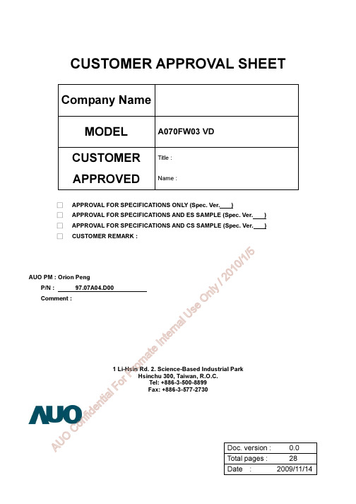
CUSTOMER APPROVAL SHEETCompany NameMODELA070FW03 VDCUSTOMERAPPROVEDTitle : Name :□ APPROVAL FOR SPECIFICATIONS ONLY (Spec. Ver. )□ APPROVAL FOR SPECIFICATIONS AND ES SAMPLE (Spec. Ver. ) □ APPROVAL FOR SPECIFICATIONS AND CS SAMPLE (Spec. Ver. ) □CUSTOMER REMARK :AUO PM : Orion PengP/N : 97.07A04.D00Comment :1 Li-Hsin Rd. 2. Science-Based Industrial ParkHsinchu 300, Taiwan, R.O.C.Tel: +886-3-500-8899 Fax: +886-3-577-2730Doc. version : 0.0 Total pages : 28A UOCo n fi de n ti a lF or Pr om a t eI nt er na l Us eOn l y / 2010/1/5Product Specification7.0" COLOR TFT-LCD MODULEModel Name :A070FW03 VDPlanned Lifetime: From 2009/Dec To2011/DecPhase-out Control:From 2011/Jul To 2011/DecEOL Schedule:2011/Jul< >Preliminary Specification < >Final SpecificationNote: The content of this specification is subject to change.© 2009 AU Optronics All Rights Reserved, Do Not Copy.A UOCo n fi de n ti a lF or Pr om a t eI nt er na l Us eOn l y / 2010/1/5Page:1/28Record of RevisionVersion Revise Date Page Content0.0 2009/03/10All First DraftA UOCo n fi de n ti a lF or Pr om a t eI nt er na l Us eOn l y / 2010/1/5Page:2/28ContentsA. General Information.....................................................................................................................................3B.Outline Dimension (4)1. TFT-LCD Module – Front View....................................................................................................................42. TFT-LCD Module – Rear View....................................................................................................................5 C.Electrical Specifications .............................................................................................................................6 1. TFT LCD Panel Pin Assignment .................................................................................................................6 2. Backlight Pin Assignment............................................................................................................................7 3. Absolute Maximum Ratings.........................................................................................................................7 3. Electrical DC Characteristics.......................................................................................................................8 4. Electrical AC Characteristics.....................................................................................................................10 6. Power On/Off Characteristics....................................................................................................................17 D. Optical Specification .................................................................................................................................18 E. Reliability Test Items .................................................................................................................................21 F.Packing and Marking.................................................................................................................................24 1. Packing Form............................................................................................................................................24 2. Module/Panel Label Information ...............................................................................................................25 3. Carton Label Information...........................................................................................................................25 G.Precautions (26)A UOCo n fi de n ti a lF or Pr om a t eI nt er na l Us eOn l y / 2010/1/5Page:3/28A. General InformationThis product is for portable DVD and digital photo frame application. NO. ItemUnit Specification Remark1 Screen Sizeinch 7.0(Diagonal)2 Display Resolution dot480RGB(W)×234(H)3 Overall Dimensionmm 164.9 (W)×100(H)×5.7(D) Note 1 4 Active Area mm154.08(W)×86.58(H) 5 Pixel Pitchmm 0.107(W)×0.370(H)6 Color Configuration --R. G. B. Stripe Note 2 7 NTSC Ratio% 48%8 Display Mode -- Normally White 9Panel surface Treatment -- Anti-Glare, 3H10 Weight g TBD 11 LCD Module Power ConsumptionW 2.212 Viewing direction6 o’clock (gray inversion)Note 1: Not include blacklight cable and FPC. Refer next page to get further information. Note 2: Below figure shows dot stripe arrangement.( 1………………………..234)A UOCo n fi de n ti a lF or Pr om aPage:4/28ALL RIGHTS STRICTLY RESERVED. ANY PORTION OF THIS PAPER SHALL NOT BE REPRODUCED, COPIED, OR TRANSFORMED TO ANY OTHER FORMSWITHOUT PERMISSION FROM AU OPTRONICS CORP.B. Outline Dimension (D00)1. TFT-LCD Module – Front ViewA UOPage:5/28ALL RIGHTS STRICTLY RESERVED. ANY PORTION OF THIS PAPER SHALL NOT BE REPRODUCED, COPIED, OR TRANSFORMED TO ANY OTHER FORMSWITHOUT PERMISSION FROM AU OPTRONICS CORP.2. TFT-LCD Module – Rear ViewA UPage:6/28C. Electrical Specifications1. TFT LCD Panel Pin AssignmentPin no Symbol I/O DescriptionRemark1 GND - Ground for logic circuit2 V CC I Supply voltage of logic control circuit for scan driver3 V GL I Negative power for scan driver4 V GH IPositive power for scan driver5 STVR I/O Vertical start pulse Note 16 STVL I/O Vertical start pulse Note 17 CKV I Shift clock input for scan driver 8 U/D I UP/DOWN scan control input Note 1,29 OEV I Output enable input for scan driver 10 VCOM I Common electrode driving signal 11 VCOM I Common electrode driving signal12 L/R I LEFT/RIGHT scan control input Note 1,213 MOD I Sequential sampling and simultaneous sampling setting14 OEH IOutput enable input for data driver15 STHL I/O Start pulse for horizontal scan lineNote 1 16 STHR I/O Start pulse for horizontal scan lineNote 1 17 CPH3 I Sampling and shifting clock pulse for data driver18 CPH2 I Sampling and shifting clock pulse for data driver19 CPH1 I Sampling and shifting clock pulse for data driver20 V CC I Supply voltage of logic control circuit for data driver21 GND - Ground for logic circuit22 VRIAlternated video signal input(Red) 23 VGI Alternated video signal input(Green) 24VBI Alternated video signal input(Blue)25 AV DD I Supply voltage for analog circuit 26AV SS-Ground for analog circuitA UOCo n fi de n ti a lF or Pr om a t eI nt er na l Us eOn l y / 2010/1/5Page:7/28I: Input pin; P: Power pin; G: Ground pin; C: capacitor pinRefer to figure as below:Pin26 Pin12. Backlight Pin AssignmentRecommended connector : E&T H201K-P020N-02BPin no Symbol I/O Description Remark1 VLEDPLED power supply2GNDLEDP LED ground3. Absolute Maximum RatingsItemSymbol Condition Min. Max. Unit RemarkV CCGND=0-0.3 7 V AV DD AGND=0-0.3 7VV GH -0.3 18 V V GL GND=0-15 0.3 V Power voltageV GH -V GL-33VV i-0.3 AV DD +0.3 VNote 3 V I-0.3 V CC +0.3 V Note 4 Input signal voltageVCOM-2.9 7.5 VNote 1: Functional operation should be restricted under ambient temperature (25℃).Note 2: Maximum ratings are those values beyond which damages to the device may occur. Functionaloperation should be restricted to the limits in the Electrical Characteristics chapter.Note 3: VR, VG, VB.Note 4: STHL, STHR, OEH, LRC, CPH1~CPH3, STVD, STVU, OEV, CKV, UDC, MODA UOCo n fi de n ti a lF or Pr om a t eI nt er na l Us eOn l y / 2010/1/5Page:8/283. Electrical DC Characteristicsa. Typical Operation Condition (AGND =GND = 0V)ItemSymbol Min. Typ. Max. Unit Remark V CC3 3.3 5.5 VDigital powerAV DD4.5 55.5 V Analog PowerV GH 14.3 15 15.7 V Positive power supply for gate driver Power VoltageVGL-10.5 -10 -9.5 V Negative power supply for gate driverV iA 0.4 - AV DD -0.4V Refer to Horizontal timing V iAC - 4- V AC component Video signal amplitude(VR,VG,VB) V iDC -AV DD /2 -VDC componentH LevelVIH 0.8xVCC - VCC VInputSignal Voltage L Level VIL GND - 0.2xVC VNote 1. V CAC 3.5 5.6 6.5 VAC component Gamma referencevoltageV CDC1.41.72.0VDC component Note 1: STHL, STHR, OEH, LRC, CPH1~CPH3, STVD, STVU, OEV, CKV, UDC, MOD.Note2: Must follow power On/Off Sequence.Note 3: If input signal amplitude is 3.3V, recommend value for Vcc is 3.3VIf input signal amplitude is 5V, recommend value for Vcc is 5Vb. Current Consumption (AGND=GND=0V)ParameterSymbol ConditionMin. Typ. Max. Unit RemarkInput current for V GH I GH V GH =15V- 0.12 1.0 m A Input current for V Gl I GL V Gl =-10V- 0.15 1.0 mA Input current for Vcc I CC DV CC =3.3- 2 6.0 mA Input current for Avdd I DDAV DD =5V-5.330mAA UOCo n fi de n ti a lF or Pr om a t eI nt er na l Us eOn l y / 2010/1/5Page:9/28c. Backlight Driving ConditionsThe backlight (LED module, Note 1) is suggested to drive by constant current with typical value.ParameterSymbol Min. Typ. Max. Unit Remark LED light bar CurrentI L-- 200 -- mABL Power ConsumptionP BL --2.1 --WNote 1 LED Life TimeL L 10,000 ---- Hr Note 2, 3Note 1: The LED driving condition is defined for LED module (24 LED). The voltage range will be 8.7 to 11.6V based on suggested driving current set as 200mA .Note 2: Define “LED Lifetime”: brightness is decreased to 50% of the initial value. LED Lifetime isrestricted under normal condition, ambient temperature = 25℃ and LED lightbar current =200mA .Note 3: If it uses larger LED lightbar voltage more than 200mA , it maybe decreases the LED lifetime.A UOCo n fi de n ti a lF or Pr om a t eI nt er na l Us eOn l y / 2Page:10/284. Electrical AC Characteristicsa. Signal AC CharacteristicsParameterSymbol Min. Typ. Max. Unit. Remark Clock cycle time t CPH100 103 107 ns CPH1 CPH pulse duty t CWH 405060%CPH1CPH pulse delay t C12 30 t CPH /3 t CPH /2 ns CPH1STH setup time t SUH 20 - - ns STHR,STHL STH hold time t HDH 20- - ns STHR,STHL STH pulse width t STH 1 t CPH STHR,STHL STH period t H 61.8 63.7 66.1 μs STHR,STHL OEH pulse width t OEH 1 - - t CPH OEH (Note 1)Sample and hold disable timet DIS1 1 - - t CPH Note 2 OEV pulse width t OEV 2.0 3.4 6.5 μs OEV CKV pulse width t CKV 1.0 3.1 4.68 μs CKV Clean enable timet DIS2 1.0- 1 t OEVμs Note 3 Horizontal display start t SH 1t CPH Horizontal display timing ranget DH 480t CPH STV setup time t SUV 400 -- ns STVU, STVD STV hold time t HDV 400 -- ns STVU, STVD STV pulse width t STV - -1t H STVU, STVDVertical display start t SV 3t H Vertical display timing ranget DV 234 t HVCOM rising time t rCOM - 5 μs VCOM falling time t fCOM- 5 μs VCOM delay time t DCOM 2 - - μs TFT charging time t ch 55 - - μs Output time delay t del 3 - - μs Setup time of analog VR/VG/VBt asu 60 - - ns Hold time of analog VR/VG/VBt ahd 40 - - ns Frame rate5060-HzNote 1: The maximum pulse width of OEH should refer to the minimum of tDIS1 and the hsyncback porch.Note 2: t DIS1 is time difference between OEH and STHL.Note 3: t DIS2 is time difference between OEV and CKVA UOCo n fi de n ti a lF or Pr om a t eI nt er na l Us eOn l y / 2010/1/5Sampling clock timingVersion:0.0Page: 15/28ALL RIGHTS STRICTLY RESERVED. ANY PORTION OF THIS PAPER SHALL NOT BE REPRODUCED, COPIED, OR TRANSFORMED TO ANY OTHER FORMS WITHOUT PERMISSION FROM AU OPTRONICS CORP.Vertical timing (From up to down)a lUs e On ly / 2010/1/5Version:0.0Page: 16/28ALL RIGHTS STRICTLY RESERVED. ANY PORTION OF THIS PAPER SHALL NOT BE REPRODUCED, COPIED, OR TRANSFORMED TO ANY OTHER FORMS WITHOUT PERMISSION FROM AU OPTRONICS CORP.Page: 17/28 6. Power On/Off CharacteristicsPower OnPage:18/28D. Optical SpecificationAll optical specification is measured under typical condition (Note 1, 2)Item Symbol Condition Min. Typ. Max. Unit Remark Response TimeRise FallTr Tfθ=0°-- --12 1824 36ms ms Note 3 Contrast ratioCRAt optimizedviewing angle 300 400 -- Note 4TopBottom LeftViewing AngleRight 30 50 50 5040 65 65 65 -- -- -- -- deg. Note 5Brightness Y Lθ=0° 320 400 -- cd/m 2 Note 6 X θ=0° 0.25 0.30 0.35 ChromaticityWhiteY θ=0° 0.27 0.32 0.37 UniformityΔY L%7075 -- %Note 7Note 1: Ambient temperature =25℃, and LED lightbar current I L = 200 mA . To be measured in the dark room.Note 2: To be measured on the center area of panel with a viewing cone of 1° by Topcon luminance meterBM-5A, after 15 minutes operation.Note 3: Definition of response time:The output signals of photo detector are measured when the input signals are changed from“black” to “white”(falling time) and from “white” to “black”(rising time), respectively.The response time is defined as the time interval between the 10% and 90% of amplitudes.Refer to figure as below.A UOCo n fi de n ti a lF or Pr om 1/5Note 4.Definition of contrast ratio:Contrast ratio is calculated with the following formula.statusBlack"" at is LCD when output detector Photo statusWhite"" at is LCD when output detector Photo (CR) ratio Contrast =Note 5. Definition of viewing angle, θ, Refer to figure as below.Note 6. Measured at the center area of the panel when all the input terminals of LCD panel areelectrically opened.Note 7: Luminance Uniformity of these 9 points is defined as below:A UOCo n fi de n ti a lF or Pr om a t eI nt er nA UOCo n fi de n ti a lF or Pr om a t eI nt er na l Us eOn l y / 2010/1/5Page:21/28E. Reliability Test ItemsNo. Test itemsConditions Remark1 High Temperature Storage240Hrs2 Low Temperature Storage Ta= -2240Hrs3 High Ttemperature Operation Tp240Hrs4 Low Temperature Operation Ta= -1 240Hrs5 High Temperature & High HumidityTp= 580% RH 240Hrs Operation6 Heat Shock -20d/1hr~70d/1hr judge 50cyclesNon-operation7 Electrostatic DischargeContact = ± 4 kV, class B Air = ± 8 kV, class BNote 4 8Image Sticking25, 4hrsNote 5Frequency range : 10~55HzStoke: 1.5mmSweep: 10 Hz ~55 Hz 2 hours for each direction of X,Y,Z9Vibration4 hours for Y directionNon-operationJIS C7021, A-10condition A : 15 minutes10 Mechanical Shock100G . 6ms, ±X,±Y,±Z3 times for each directionNon-operation JIS C7021,A-7condition C 11 Vibration (With Carton)Random vibration:0.015G 2/Hz from 5~200Hz–6dB/Octave from 200~500Hz IEC 68-3412 Drop (With Carton)Height: 60cm1 corner, 3 edges, 6 surfaces13 Pressure5kg, 5sec Note 6Note 1: Ta: Ambient Temperature. Tp: Panel Surface TemperatureNote 2: In the standard conditions, there is not display function NG issue occurred. All the cosmeticspecification is judged before the reliability stress.Note 3: All the cosmetic specification is judged before the reliability stress.Note 4 : All test techniques follow IEC6100-4-2 standard.A UOCo n fi de n ti a lF or Pr om a t eI nt er na l Us eOn l y / 2010/1/5Page:22/28Contact Discharge :330Ω, 150pF, 1sec, 8 point, 25times/pointgray pattern. After 20 minutes, the mura is less than JND 2.5Note 6: The panel is tested as figure. The jig is ψ10 mm made by Cu with rubber and the loadingspeed is 3mm/min on position 1~5. After the condition, no glass crack will be found and panelfunction check is OK.( no guarantee LC mura 、LC bubble)A UOCo n fi de n ti a lF or Pr om a t eI nt eUs eOn l y / 201Page:23/28A UOCo n fi de n ti a lF or Pr om a t eI nt er na l Us eOn l y / 2010/1/5Page:24/28F. Packing and Marking1. Packing FormA UOCo n fi de n ti a lF or Pn l y2. Module/Panel Label InformationThe module/panel (collectively called as the “Product”) will be attached with a label of Shipping Numberwhich represents the identification of the Product at a specific location. Refer to the Product outline drawing for detailed location and size of the label. The label is composed of a 22-digit serial number and printed with code128 with the following definition:Example:501M06ZL06123456781Z05: Product Manufacturing Week Code: WK50 Product Version: Version 1 Product Manufactuing Factory: M063. Carton Label InformationThe packing carton will be attached with a carton label where packing Q’ty, AUO Model Name, AUO PartNumber, Customer Part Number (Optional) and a series of Carton Number in 13 or 14 digits are printed. TheCarton Number is apparing in the following format:Refer to the drawing of packing format for the location and size of the carton label.A UOCo n fi de n ti a lF or Pr om a t eI nt er na l Us eOn l y / 2010/1/5G. Precautions1. Do not twist or bend the module and prevent the unsuitable external force for display module during assembly.2. Adopt measures for good heat radiation. Be sure to use the module with in the specified temperature.3. Avoid dust or oil mist during assembly.4. Follow the correct power sequence while operating. Do not apply the invalid signal, otherwise, it will cause improper shut down and damage the module.5. Less EMI: it will be more safety and less noise.6. Please operate module in suitable temperature. The response time & brightness will drift by different temperature.7. Avoid to display the fixed pattern (exclude the white pattern) in a long period, otherwise, it will cause image sticking.8. Be sure to turn off the power when connecting or disconnecting the circuit. 9. Polarizer scratches easily, please handle it carefully. 10. Display surface never likes dirt or stains.11. A dewdrop may lead to destruction. Please wipe off any moisture before using module.12. Sudden temperature changes cause condensation, and it will cause polarizer damaged.13. High temperature and humidity may degrade performance. Please do not expose the module to the direct sunlight and so on.14. Acetic acid or chlorine compounds are not friends with TFT display module.15. Static electricity will damage the module, please do not touch the module without any groundeddevice.16. Do not disassemble and reassemble the module by self.17. Be careful do not touch the rear side directly.18. No strong vibration or shock. It will cause module broken.19. Storage the modules in suitable environment with regular packing.20. Be careful of injury from a broken display module.21. Please avoid the pressure adding to the surface (front or rear side) of modules, because it will causethe display non-uniformity or other function issue.A UOCo n fi de n ti a lF or Pr om a t eI nt er na l Us eOn l y / 2010/1/5。
philips 170x6 lcd monitor 电子用户手册说明书
Safety and Troubleshooting Information•安全措施及维修• 安装地点• 常见问题• 故障检修• 有关规定• 其他相关信息安全和故障检修安全措施与维修警告:使用本文件规定以外的控制、调整或程序,可能导致遭受电击、触电以及/或者机械危险。
连接和使用电脑显示器时,请阅读并遵循以下说明:● 为保护显示器不受损坏,请勿过分用力按 LCD 面板。
移动显示器时,请握住两侧边框;抬起显示器时,请勿将手或手指放在 LCD 面板上。
● 如果较长时间不准备使用显示器,应拔出显示器电源插头。
● 如需用微潮的布擦试显示器,应拔出电源插头。
当电源切断时可用干布擦试屏幕,但切不可使用酒精、溶剂或含氨的液体。
● 如果遵守本手册说明时显示器仍不能正常运转,应向维修技师查询。
● 外壳应只有合格维修人员方可打开。
● 显示器应避免直接日晒,勿靠近火炉或其他热源。
● 任何可能掉入孔口或妨碍显示器各电子元件正常降温的物体皆应挪开。
● 勿阻塞机体通风口。
● 保持显示器干燥。
为防电击起见,勿将其暴露于雨中或过多湿气中。
● 放置显示器时,确信电源插头和输出口容易取用。
● 如果以拔出电源线或直流电电源线之方式关闭显示器,6 秒钟方可再插入电源线或直流电电源线以便重新正常运转。
● 为防止机身遭受电击或永久性损坏,勿将显示器暴露于雨中或过多湿气中。
● 请注意:在使用应用程序时请保持启动一个屏幕保护程序。
如果一个高对比度的图象长时间停留在屏幕上时,该图象将在你的屏幕上产生一个所谓的“殘影”或“鬼影”。
这在LCD技术固有的一些缺陷中是常见的现象。
通常在关闭显示器电源后,该殘影会逐渐消失。
值得注意的是,这种殘影症状是无法修复的,并不属于保修范围之内● 提起显示器时应特别注意 - 不要使用标志盖下面的区域来抓住或提起显示器。
在标志盖上用力可能会使它从显示器主体上脱落,从而使显示器跌落。
提起显示器时,应把一只手托在显示器框架的下面。
奇美7寸液晶屏HE070NA-13C 规格书

CHIMEI INNO L U X DISPLAY CORPORATIONLCD MODULESPECIFICATIONCustomer: Model Name: HE070NA-13CDate: 2012/08/27 Version:01■Preliminary Specification □Final SpecificationFor Customer ’s AcceptanceApproved byCommentApproved byReviewed byPrepared by Stanely CW Leung 2012/08/Wenyi Wang2012/08/Sunny Sun2012/08/ Approved byReviewed byPrepared by深显实业有限公司 CHIMEI InnoLux copyright2004All rights reserved,Copying forbidden. Record of RevisionVersion ReviseDatePage ContentPre-Spec.01 2012/08/27 All Initial Release.CHIMEI INNO L U XContents1.General Specifications (1)2.Pin Assignment (2)3.Operation Specifications....................................................................錯誤! 尚未定義書籤。
3.1. Absolute Maximum Ratings (5)3.1.1. Typical Operation Conditions (6)3.1.2. Current Consumption (7)3.2. Power Sequence (8)3.3. Timing Characteristics (9)3.3.1. AC Electrical Characteristics (9)3.3.2. Input Clock and Data Timing Diagram (9)3.3.3. DC Electrical Characteristics (10)3.3.4. Timing (11)3.3.5. Data Input Format (12)4.Optical Specifications (13)5.Reliability Test Items (16)6.General Precautions (17)6.1. Safety (17)6.2. Handling (17)6.3. Static Electricity (17)6.4. Storage (17)6.5. Cleaning (17)7.Mechanical Drawing (18)8.Package Drawing (19)8.1. Packaging Material Table (19)8.2. Packaging Quantity (19)8.3. Packaging Drawing (20)1. General SpecificationsNo. Item Specification Remark1 LCD size 7.0 inch(Diagonal)2 Driver element a-Si TFT active matrix3 Resolution 1024 × 3(RGB) × 6004 Display mode Normally White, Transmissive5 Dot pitch 0.05(W) × 0.15(H) mm6 Active area 153.6(W) × 90.0(H) mm7 Panel size 160(W) × 101.1(H) ×1.3 (D) mm Note 18 Surface treatment Anti-Glare9 Color arrangement RGB-stripe10 Interface Digital11 Panel power consumption TBD12 Weight TBD(Typ.)Note 1: Refer to Mechanical Drawing.2. Pin AssignmentFPC Connector is used for the module electronics interface. The recommended model is FH12A-40S-0.5SH manufactured by Hirose.Pin No. Symbol I/O Function Remark1 VCOM P Common Voltage2 VDD P Power Voltage for digital circuit3 VDD P Power Voltage for digital circuit4 NC --- No connection5 Reset I Global reset pin6 STBYB I Standby mode, Normally pulled high STBYB = “1”, normal operation STBYB = “0”, timing controller, source driver will turn off, all output are High-Z7 GND P Ground8 RXIN0- I - LVDS differential data input9 RXIN0+ I + LVDS differential data input10 GND P Ground11 RXIN1- I - LVDS differential data input12 RXIN1+ I + LVDS differential data input13 GND P Ground14 RXIN2- I - LVDS differential data input15 RXIN2+ I + LVDS differential data input16 GND P Ground17 RXCLKIN- I - LVDS differential clock input18 RXCLKIN+ I + LVDS differential clock input19 GND P Ground20 RXIN3- I - LVDS differential data input21 RXIN3+ I + LVDS differential data input22 GND P Ground23 NC --- No connection24 NC --- No connection25 GND P Ground26 NC --- No connection27 DIMO O Backlight CABC controller signal output28 SELB I 6bit/8bit mode select Note129 AVDD P Power for Analog Circuit30 GND P Ground31 LED- P LED Cathode32 LED- P LED Cathode33 L/R I Horizontal inversion Note334 U/D I Vertical inversion Note335 VGL P Gate OFF Voltage36 CABCEN1 I CABC H/W enable Note237 CABCEN0 I CABC H/W enable Note238 VGH P Gate ON Voltage39 LED+ P LED Anode40 LED+ P LED AnodeI: input, O: output, P: PowerNote1: If LVDS input data is 6 bits ,SELB must be set to High;If LVDS input data is 8 bits ,SELB must be set to Low.Note2: When CABC_EN=”00”, CABC OFF.When CABC_EN=”01”, user interface image.When CABC_EN=”10”, still picture.When CABC_EN=”11”, moving image.When CABC off, don’t connect DIMO, else connect it to backlight. Note3: When L/R=”0”, set right to left scan direction.When L/R=”1”, set left to right scan direction.When U/D=”0”, set top to bottom scan direction.When U/D=”1”, set bottom to top scan direction.Note: Definition of scanning direction.Refer to the figure as below:3. Operation Specifications3.1. Absolute Maximum Ratings(Note 1)ValuesUnit Remark Item SymbolMin. Max.DV DD -0.3 5.0 VAV DD 6.5 13.5 V Power voltageV GH -0.3 42.0 VV GL -20.0 0.3 VV GH-V GL- 40.0 V Operation Temperature T OP -20 60 ℃Storage Temperature T ST-30 70 ℃Note 1: The absolute maximum rating values of this product are not allowed to be exceeded at any times. Should a module be used with any of the absolute maximum ratingsexceeded, the characteristics of the module may not be recovered, or in an extremecase, the module may be permanently destroyed.3.1.1. Typical Operation Conditions( Note 1)ValuesUnit Remark Item SymbolMin. Typ. Max.DV DD 3.0 3.3 3.6 V Note 2AV DD 10.8 11 11.2 VPower voltageV GH 19.7 20 20.3 VV GL -6.5 -6.8 -7.1 VInput signal voltage V COM 3.4 (3.7) 4.0 V Note 4Input logic high voltage V IH 0.7 DV DD - DV DD VNote 3 Input logic low voltage V IL 0 - 0.3 DV DD VNote 1: Be sure to apply DV DD and V GL to the LCD first, and then apply V GH.Note 2: DV DD setting should match the signals output voltage (refer to Note 3) of customer’s system board.Note 3: LVDS,Reset.Note 4: Typ. V COM is only a reference value, it must be optimized according to each LCM.Be sure to use VR;3.1.2. Current ConsumptionValuesItem SymbolMin. Typ. Max.Unit RemarkI GH - 0.25 1.0 mA V GH =20VI GL - 0.25 1.0 mA V GL = -6.8V IDV DD - 38 60 mA DV DD =3.3VCurrent for DriverIAV DD - 20 30 mA AV DD =11V3.2. Power Sequencea. Power on:b. Power off:VDD STBYB RESET A VGL VGHLVDS Signal >50ms>100ms>=0msNormal signalVCOM <20msVDD STBYB RESET A VGL VGHLVDS Signal>50us>40us>20us <20ms<500us >500usNormal signalVCOM >35ms3.3. Timing Characteristics3.3.1. AC Electrical CharacteristicsValuesParameter SymbolUnit RemarkMin. Typ. Max.Clock frequency R xFCLK40.8 51.2 67.2 MHzInput data skew margin T RSKM500 - - psClock high time T LVCH- 4/(7* R xFCLK) - nsClock low time T LVCL- 3/(7* R xFCLK) - ns3.3.2. Input Clock and Data Timing Diagram3.3.3. DC Electrical CharacteristicsValuesParameter SymbolMin. Typ. Max.Unit RemarkDifferential input highThreshold voltageR xVTH- - +0.1 VDifferential input low Threshold voltage R xVTL-0.1 - - VR XVCM=1.2VInput voltage range(singled-end)R xVIN0 - 2.4 V Differential input common modevoltageR xVCM|V ID|/2 - 2.4-|V ID|/2 V Differential voltage|V ID|0.2 - 0.6 V Differential input leakage current RV xliz-10 - +10 uA3.3.4. TimingValuesItem SymbolMin. Typ. Max.Unit RemarkClock Frequency fclk 40.8 51.2 67.2 MHz Frame rate =60HzHorizontal display area thd1024 DCLK HS period time th1114 1344 1400 DCLK HS Blanking thb90 320 376 DCLK Vertical display area tvd600 H VS period time tv610 635 800 H VS Blanking thb10 35 200 H3.3.5. Data Input Format6bit LVDS input8bit LVDS inputNote: Support DE timing mode only, SYNC mode not supported.4. O ptical SpecificationsNote: Base on CHIMEI-INNOLUX LCMValuesItemSymbolConditionMin.Typ. Max. UnitRemarkθLΦ=180°(9 o’clock) 75 85 - θR Φ=0°(3 o’clock) 75 85 -θT Φ=90°(12 o’clock) 75 85 - Viewing angle (CR≥ 10) B/L ONθB Φ=270°(6 o’clock)75 85 - degree Note 1 T ON- 10 20 msec Response timeT OFF-15 30 msec Note2 Note 3 Contrast ratioCR 400500-- Note 4 Note 6 W X0.249 0.299 0.349- Color chromaticityW Y0.273 0.323 0.373 - Note 2 Note 5 TransmittanceTrNormal θ=Φ=0°-(2.8%)-Test Conditions:1. DV DD =3.3V, the ambient temperature is 25℃.2. The test systems refer to Note 2.Fig. 4-1 Definition of viewing angleNote 2: Definition of optical measurement system.The optical characteristics should be measured in dark room. After 30 minutes operation, the optical properties are measured at the center point of the LCD screen. (Viewing angle is measured by ELDIM-EZ contrast/Height :1.2mm, Response time is measured by Photo detector TOPCON BM-7, other items are measured by BM-5A/ Field of view: 1° /Height: 500mm.)Fig. 4-2 Optical measurement system setupNormal line θ=Φ=0°Photo detectorΦ=90°12 o’clock directionΦ=270°6 o’clock directionΦ=0°Φ=180°Active Area500mmLCMθ=Φ=0°Φ=90°12 o’clock direction Φ=270°6 o’clock direction Φ=0°Φ=180°Active AreaθLθTθBθRLCMNote 3: Definition of Response timeThe response time is defined as the LCD optical switching time interval between“White” state and “Black” state. Rise time (T ON ) is the time between photo detector output intensity changed from 90% to 10%. And fall time (T OFF ) is the time between photo detector output intensity changed from 10% to 90%.Fig. 4-3 Definition of response timeNote 4: Definition of contrast ratiostate Black"" the on LCD when measured Luminance state White"" the on LCD when measured Luminance (CR) ratio Contrast =Note 5: Definition of backlightThe backlight used C light.Note 6: base on CMI standard backlight structure of LCM90%10% 0%P h o t o d e t e c t o r o u t p u t (R e l a t i v e v a l u e )ONT White (TFT OFF)Black (TFT ON)White (TFT OFF)5. Reliability Test Items(Note3)Item Test Conditions Remark High Temperature Storage Ta = 70℃120hrs Note 1,Note 4 Low Temperature Storage Ta = -30℃120hrs Note 1,Note 4 High Temperature Operation Ts = 60℃120hrs Note 2,Note 4 Low Temperature Operation Ta = -20℃120hrs Note 1,Note 4 Operate at High Temperatureand Humidity+40℃, 90%RH 120hrs Note 4Thermal Shock -20℃/30 min ~ +60℃/30 min for a total 100cycles, Start with cold temperature and endwith high temperature.Note 4Note 1: Ta is the ambient temperature of samples.Note 2: Ts is the temperature of panel’s surface.Note 3: In the standard condition, there shall be no practical problem that may affect the display function. After the reliability test, the product only guarantees operation,but don’t guarantee all of the cosmetic specification.Note 4: Before cosmetic and function test, the product must have enough recovery time, at least 2 hours at room temperature.6. General Precautions6.1. SafetyLiquid crystal is poisonous. Do not put it in your mouth. If liquid crystal touches your skin or clothes, wash it off immediately by using soap and water.6.2. Handling1. The LCD panel is plate glass. Do not subject the panel to mechanical shock or toexcessive force on its surface.2. The polarizer attached to the display is easily damaged. Please handle it carefullyto avoid scratch or other damages.3. To avoid contamination on the display surface, do not touch the module surfacewith bare hands.4. Keep a space so that the LCD panels do not touch other components.5. Put cover board such as acrylic board on the surface of LCD panel to protect panelfrom damages.6. Transparent electrodes may be disconnected if you use the LCD panel underenvironmental conditions where the condensation of dew occurs.7. Do not leave module in direct sunlight to avoid malfunction of the ICs.6.3. Static Electricity1. Be sure to ground module before turning on power or operating module.2. Do not apply voltage which exceeds the absolute maximum rating value.6.4. Storage1. Store the module in a dark room where must keep at 25±10℃ and 65%RH or less.2. Do not store the module in surroundings containing organic solvent or corrosivegas.3. Store the module in an anti-electrostatic container or bag.6.5. Cleaning1. Do not wipe the polarizer with dry cloth. It might cause scratch.2. Only use a soft sloth with IPA to wipe the polarizer, other chemicals mightpermanent damage to the polarizer.7. Mechanical Drawing深显实业有限公司8. Package Drawing8.1. Packaging Material TableNo. ItemModel(Material)Dimensions(mm)UnitWeight(kg)Quantity Remark1 PanelAssemblyHE070NA-13C 160.00 × 147.95 ×1.3 TBD 802 Dust-Proof BagPE 700 x 530 0.050 13 Tray PET 505 x 338 x16.5 0.22 21 Anti-static4 Partition Corrugatedpaper512 × 350 x 225 0.29 15 Carton Corrugatedpaper530 × 355 × 255 0.81 18 Total weight TBD± 5%Kg8.2. Packaging QuantityTotal LCM quantity in Carton:no. of Trays(deduct a empty tray) (21-1) × quantity per Tray 4 = 80 PCS8.3. Packaging Drawing。
研工(KinSoon)70寸户外高亮液晶屏KSN700SN01-A01规格书

Power Supply Voltage Storage temperatuቤተ መጻሕፍቲ ባይዱe
Glass surface temperature (Operation) Center T. Uniformity
VDD TSTG
TCENTER
△T
GND-0.5 -20
0 -
13.2 65
50 10
V ℃
℃ ℃
(1) (2)
MODEL
KSN700SN01-A01
Doc. No
12-24-0206
Page
4 / 28
1. Absolute Maximum Ratings
If the condition exceeds maximum ratings, it can cause malfunction or unrecoverable damage to the device. Item Symbol Min. Max. Unit Note
(2),(3)
Note (1) Ta= 25 ± 2 °C (2) Temperature and relative humidity range are shown in the figure below. a. 90 % RH Max. (Ta ≤ 39 °C) b. Relative Humidity is 90% or less. (Ta > 39 °C) c. No condensation (3) If panels are under low temperature(below 0 °C) or high humidity(over 35%) storage condition Panels should be left 4hours in room temperature without operation and with 8-hour aging before normal operation.
操控装置-液晶屏显示通用说明书范文2022第1版-图文
操控装置-液晶屏显示通用说明书范文2022第1版-图文液晶屏系列开关柜综合智能操控装置安装使用说明书(中性)开关柜综合智能操控装置目录一、引用标准...........................................1二、产品概述...........................................1三、技术参数...........................................1四、前面板示意图及说明..................................1五、背部端子示意图及说明................................3六、主要功能...........................................3七、安装屏开孔........................................10八、外形尺寸图........................................10九、通讯指南..........................................11十、使用注意事项......................................14十一、运输储存........................................14十二、通讯指南. (14)2一.引用标准DL/T538-2006《高压带电显示装置技术条件》二.产品概述液晶开关状态智能操控装置是根据目前中高压开关柜技术发展而开发设计的一种新型多功能、智能化动态模拟显示及操控装置,适用于中置柜、手车柜、固定柜、环网柜等多种成套装置上。
它集开关柜一次回路模拟图、手车(隔离刀)位置、断路器位置(分、合闸状态、弹簧储能状态)、接地闸刀位置等,高压带电显示(带自检)、带电闭锁、缺相报警、开关柜内环境温湿度的检控及故障显示、分/合闸、远方/就地、手储/自储控制、柜内照明、RS485通讯等功能于一体。
7寸单锭显示器说明书

2 / 25
1、安全注意事项:
按下为静音按键 向左旋转为音量减; 向右旋转为音量加
¾
面板插孔 孔说明:
A B C D A : 耳机插孔 耳 , 方便前置的耳 方 耳机输出, 当插 插入耳机, 功放将静音 功 . B : USB U 插孔, 仅在电脑开机 仅 且后端的 US SB 连接到电脑 脑时才有效,方便电脑读 U 盘 仅 机且后端的 USB U 连接到电 电脑时才有效 效,方便电脑读 读 SD 卡 C : SD 卡插座, 仅在电脑开机 D : CF C 卡插座, 仅在电脑开机 仅 机且后端的 USB U 连接到电 电脑时才有效 效,方便电脑读 读 CF 卡
警告 提示
2、功能特点 ....................... 3 3、使用之前 ....................... 4
整机外观及按键基本功能 遥控器按键功能
4、显示器操作 ....................... 6
打开/关闭显示屏 倒车自动显示 车载 PC 的开关机控制 静音操作: 模式转换操作:
8、整机规格参数 ...................... 23
2、功能特点:
TFT 液晶显示屏:
采用车载专用数字 TFT 屏 高分辨率:800X480XRGB 高亮度:最高可达 450cd/m 高对比率:最高可达 500 宽视角: 上 >70℃ 下 >70℃ 左 >70℃ 右 >70℃ 长寿命背光源: 》10000 小时 宽使用温度范围:-20℃至+85℃
VGA 接口:
支持显示模式多,最高达到 1024X768 支持 SOG 同步输入模式 可以支持非标准显示模式.
70寸液晶智能触摸一体机参数

交流电:100~240伏60/50赫兹
整机功率
≤180W
省电功耗
电视:<0.5瓦;电脑:<3瓦
附件
说明书,保修卡,合格证,遥控器,电池,电源线,VGA线,电脑音频线,触摸连接线,触摸光盘,触摸笔
净重(裸机)
49kg
毛重(包装)
53kg
环境因素
操作温度:0℃~40℃
操作湿度:10%~80%
贮藏温度:-20℃~40℃
7、设有化学、数学、物理学科需使用的工具数学工具:其中数学公式识别;数学公式及数学函数图;设有直尺、三角板、圆规、量角器等工具,可画线、画圆、拉伸、旋转。
8、不同效果应用设计不同工具,例如:手写识别、文本编辑、放大镜、聚光灯、遮幕、日历、时钟、屏幕录制、回放等适用工具。
★9、画词搜索:在软件页面上写出关键词,选中画词搜索圈中关键词即可在本地资料库或网络上搜索相关资料,能迅速调出教学需要的资料方便教学.
13、允许用户在键盘上按“Ctrl + V”粘贴外部复制好的图片
★14、允许用户把电脑上的工具添加到软件中
15、提供资源库,内容并包括图片和多媒体,提供指定资源库管理目录,支持对资源库内容的整理、新增、导入、导出功能;可超链接打开电脑桌面或其他外部程序文件。
输入端子
视频输入
同轴天线端口:一组
复合视频输入端口:二组
S端子:一组
15针电脑VGA接口:3组(一组前置)
色差端子:一组
多媒体USB:两组(一组前置)
电脑USB接口:六组前置电脑USB拓展接口两组
高清晰度多媒体接口(HDMI):四组(一组前置、一组内置)
串口控制输入
RS232串口控制端口:一组(连接电脑实现电脑控制电视功能)
友达7寸液晶屏G070VW01 V002规格书-杭州旭虹科技有限公司
□Preliminary Specifications■Final SpecificationsModule 7.0 Inch Color TFT-LCD Model Name G070VW01 V002Customer DateChecked &Approved byNote: This Specification is subject to change without notice. Approved by Date Grace Hung 2016/06/30 Prepared byRyan Chen 2016/06/30 General Display Business Division / AU Optronics corporation1. Operating Precautions (4)2. General Description (5)2.1 Display Characteristics (5)2.2 Optical Characteristics (6)3. Functional Block Diagram (9)4. Absolute Maximum Ratings (10)4.1 Absolute Ratings of TFT LCD Module (10)4.2 Absolute Ratings of Environment (10)5. Electrical Characteristics (11)5.1 TFT LCD Module (11)5.2 Backlight Unit (13)6. Signal Characteristic (14)6.1 Pixel Format Image (14)6.2 Signal Description (15)6.3 Scanning Direction (16)6.4 The Input Data Format (17)6.5 Interface Timing (18)6.6 Power ON/OFF Sequence (19)7. Connector & Pin Assignment (19)7.1 TFT LCD Signal (CN1): LVDS Connector (20)7.2 LED Backlight Unit (CN2): LED Driver Connector (20)7.3 LED Light Bar Input Connector (CN4): (21)8. Reliability Test Criteria (21)9. Mechanical Characteristics (22)9.1 LCM Front View (22)9.2 LCM Rear View (23)10. Label and Packaging (24)10.1 Shipping Label (on the rear side of TFT-LCD display) (24)10.2 Carton Package (24)11 Safety (25)11 Safety (25)11.1 Sharp Edge Requirements (25)11.2 Materials (25)11.3 Capacitors (25)11.4 National Test Lab Requirement (25)Record of RevisionVersion and Date Page Old description New Description0.0 2008/10/17 All First Edition0.1 2008/12/18 18 LED Backlight Unit (CN2) Pin description Pin description has been corrected. 0.2 2009/01/086 Viewing Angle(L/R/U/D)80/80/60/80 (Typ.); 70/70/55/65 (Min.) Viewing Angle(L/R/U/D)80/80/80/80 (Typ.); 70/70/70/70 (Min.) 18Dimming: Analog, 0.3~1.2V (10~100%) Dimming: Analog, 0~5V (10~100%) 0.3 2009/03/02 5 Typical power consumption 4.2w Typical power consumption 3.7w 5 Wieght :165 ± 10 g 6 Uniformity:1.311 Update 5.1.1 Power specification13 Update 5.2.1 Parameter guideline for LED 17 Update 6.6 Power ON/OFF Sequence 18 Update 6.5.1 Timing characteristics 20 Update 7.2 Pin descripiton 24Update 10. Label and Packageing 1.0 2009/04/23 20LVDS Connector:Add Manufacturer: STM Connector Model Number: Add STM-MSB24013P20HA Mating Model Number: Add STM-P24013P206 Contrast Ratio: 500(Typ) Contrast Ratio: 1000(Typ); 750(min) 6 Update Color / Chromaticity Coordinates13Update min Swing Voltage=0.3V1.1 2009/05/1513 Add the description of LED Light Bar in 5.2.121 Add 7.3 LED Light Bar Input Connector description23Add the description of LED Light Bar connector in LCM Rear View1.2 2011/09/01 10Add the graph of temp v.s humidity 1.3 2012/12/10 6 Contract Ratio: 1000(Typ); 750(min) Contract Ratio: 750(Typ); 500(min) 1.4 2013/05/13 13 Add Display ON/OFF voltage range1.5 2014/05/21 15Pin19:VDD & PIN20:GND for 6 Bit Input Mode1.6 2016/06/30 5 Must be tied to Ground in 6 bit input mode.Update Typical Power Consumption 3.7 ->2.52 Watt13Update Parameter guideline for LED table1. Operating Precautions1) Since front polarizer is easily damaged, please be cautious not to scratch it.2) Be sure to turn off power supply when inserting or disconnecting from input connector.3) Wipe off water drop immediately. Long contact with water may cause discoloration or spots.4) When the panel surface is soiled, wipe it with absorbent cotton or soft cloth.5) Since the panel is made of glass, it may be broken or cracked if dropped or bumped on hardsurface.6) To avoid ESD (Electro Static Discharge) damage, be sure to ground yourself before handlingTFT-LCD Module.7) Do not open nor modify the module assembly.8) Do not press the reflector sheet at the back of the module to any direction.9) In case if a module has to be put back into the packing container slot after it was taken outfrom the container, do not press the center of the LED Reflector edge. Instead, press at the far ends of the LED Reflector edge softly. Otherwise the TFT Module may be damaged.10) A t the insertion or removal of the Signal Interface Connector, be sure not to rotate nor tilt theInterface Connector of the TFT Module.11) A fter installation of the TFT Module into an enclosure (Notebook PC Bezel, for example), donot twist nor bend the TFT Module even momentary. At designing the enclosure, it should be taken into consideration that no bending/twisting forces are applied to the TFT Module from outside. Otherwise the TFT Module may be damaged.12) S mall amount of materials having no flammability grade is used in the LCD module. The LCDmodule should be supplied by power complied with requirements of Limited Power Source (IEC60950 or UL1950), or be applied exemption.13) S evere temperature condition may result in different luminance, response time.14) C ontinuous operating TFT-LCD Module under high temperature environment may accelerateLED light bar exhaustion and reduce luminance dramatically.15) T he data on this specification sheet is applicable when LCD module is placed in landscapeposition.16) C ontinuous displaying fixed pattern may induce image sticking. It is recommended to usescreen saver or shuffle content periodically if fixed pattern is displayed on the screen.G070VW01 V0022. General DescriptionThis specification applies to the 7.0 inch color TFT LCD module G070VW01 V0.G070VW01 V0 designed with wide viewing angle; wide operating temperature and long life LEDs backlight is well suited to be the display units for Industrial Applications.LED driving board for backlight unit is included in this panel and the structure of the LED units is replaceable.G070VW01 V0 is built in timing controller and LVDS interface.The screen format is intended to support the WVGA (800(H) x 480(V)) screen and 16.2M (RGB 8-bits) or 262k colors (RGB 6-bits).G070VW01 V0 is a RoHS product.2.1 Display CharacteristicsThe following items are characteristics summary on the table under 25 ℃ condition:Items Unit SpecificationsScreen Diagonal [inch] 7.0 ( 177.8mm )Active Area [mm] 152.40(H) x 91.44(V)Pixels H x V 800x3(RGB) x 480Pixel Pitch [mm] 0.1905x 0.1905Pixel Arrangement R.G.B. Vertical StripeDisplay Mode TN, Normally WhiteNominal Input Voltage VDD [Volt] 3.3 typ.Typical Power Consumption [Watt] 2.52 typ.Weight [Grams] 165 ±10Physical Size [mm] 170.0(W) x 111.0(H) x 7.5(D) (typ.)Electrical Interface 1 channel LVDSSurface Treatment Anti-glare, Hardness 3HSupport Color 262K(6-bit) / 16.2M(8-bit)Temperature RangeOperatingStorage (Non-Operating) [o C][o C]-30 to +85 (panel surface temperature)-30 to +85RoHS Compliance RoHS ComplianceG070VW01 V0022.2 Optical CharacteristicsThe optical characteristics are measured under stable conditions at 25℃ (Room Temperature):Item Unit Conditions Min. Typ. Max.Note White Luminance[cd/m2] I F = 50mA(center point) 300 400 -1Uniformity 5 Points - 1.3 1.2.3 Contrast Ratio500 750 - 4Response Time[msec]Rising - 20 30 5 [msec] Falling - 10 20 [msec] Rising + Falling - 30 50 Viewing Angle[degree] [degree]Horizontal (Right) CR ≧10 (Left)70 70 80 80 - - 6 [degree] [degree]Vertical (Upper) CR ≧10 (Lower) 70 70 80 80 - - Color / Chromaticity Coordinates (CIE 1931)Red x 0.55 0.60 0.65 1Red y 0.30 0.35 0.40 Green x 0.27 0.32 0.37 Green y 0.55 0.60 0.65 Blue x 0.10 0.15 0.20 Blue y 0.03 0.08 0.13 White x 0.26 0.31 0.36 White y 0.28 0.33 0.38 Color Gamut% -60-1Note 1: Measurement methodEquipment : Pattern Generator, Power Supply, Digital Voltmeter, Luminance meter (SR_3 or equivalent)Aperture1with 50cm viewing distance ∘Test Point Center Environment < 1 luxModule Driving EquipmentG070VW01 V002Note 2: Definition of 5 points position (Display active area: 152.40(H) x 91.44(V))Note 3:The luminance uniformity of 5 points is defined by dividing the maximum luminance value by the minimum luminance value at full white condition.Note 4: Definition of contrast ratio (CR):Note 5: Definition of response time:The output signals of photo detector are measured when the input signals are changed from “White” to “Black”(falling time) and from “Black” to “White” (rising time), respectively. The response time interval is between 10% and 90% of amplitudes. Please refer to the figure as below.Contrast ratio (CR)=Brightness on the “White” state Brightness on the “Black” stateMaximum Brightness of five pointsδW5 = Minimum Brightness of five points G070VW01 V002Note 6: Definition of viewing angleViewing angle is the measurement of contrast ratio 10, at the screen center, over a 180° horizontal and 180°≧vertical range (off-normal viewing angles). The 180° viewing angle range is broken down as below: 90° (θ) horizontal left and right, and 90° (Φ) vertical high (up) and low (down). The measurement direction is typically perpendicular to the display surface with the screen rotated to its center to develop the desired measurement viewing angle.G070VW01 V0023. Functional Block DiagramThe following diagram shows the functional block of the 7.0 inch color TFT/LCD module:G070VW01 V0024. Absolute Maximum Ratings4.1 Absolute Ratings of TFT LCD ModuleItem Symbol Min Max Unit Conditions Logic/LCD Drive Voltage VDD -0.3 +3.6 [Volt]4.2 Absolute Ratings of EnvironmentItem Symbol Min Max UnitOperating Temperature TOP -30 +85 [o C]Operation Humidity HOP 5 90 [%RH]Storage Temperature TST -30 +85 [o C]Storage Humidity HST 5 90 [%RH]Note: Maximum Wet-Bulb should be 39 and no condensation.℃G070VW01 V002G070VW01 V002工业液晶屏www.hzxuhong.com5. Electrical Characteristics 5.1 TFT LCD Module5.1.1 Power SpecificationSymbol Parameter Logic/LCD Drive Voltage VDD Current LCD Inrush Current VDD Power Min 3.0 Typ 3.3 240 0.8 Max 3.6 260 3 0.96 Units [Volt] [mA] [A] [Watt]VDD IVDD Irush PVDD±10%Remark64 Gray Bar Pattern (VDD=3.3V, at 60Hz) Note 1 64 Gray Bar Pattern (VDD=3.3V, at 60Hz)Note 1: Measurement condition:+3.3V D6 D5 D2 D1 R1 47K G Q3 AO6402 F1 SVDD VCC(LCD Module Input)C1 1uF/16V(High to Low) Control SignalD1 D2 D5 D6 R2 G 1K C3 S Q3 AO6402 VR1 47K 0.01uF/25V2+12.0V SW1 SW MAG-SPST1R21K C2 1uF/25V90%3.3V10% 0V 470msVDD rising time64 Gray patternG070VW01 V00211/25G070VW01 V002工业液晶屏www.hzxuhong.com5.1.2 Signal Electrical CharacteristicsInput signals shall be low or Hi-Z state when VDD is off.Symbol VTH VTLItem Differential Input High Threshold Differential Input Low Threshold Input Differential Voltage Differential Input Common Mode VoltageMin. -100 100 1.1Typ. 400Max. 100 600 1.6UnitRemark[mV] VICM=1.2V [mV] VICM=1.2V [mV] [V] VTH/VTL= 100mV|VID|VICM±Note: LVDS Signal Waveform.VICMG070VW01 V00212/25G070VW01 V002工业液晶屏www.hzxuhong.com5.2 Backlight Unit5.2.1 Parameter guideline for LEDFollowing characteristics are measured under a stable condition using an inverter at 25 Symbol VCC Ivcc PVCC Irush LED Dimming Display ON/OFF Off Control Voltage Brightness 25 percentage IF LED Forward Current VF LED Forward Voltage PLED Operation Lifetime LED Power Consumption 50,000 50 (33) 30.5 (28.7) 1.525 (41.8) 39.05 (37.07)Watt Hrs mA [Volt] [Volt] Ta = 25 C IF = 50mA, Ta = -30 C IF = 50mA, Ta = 25 C IF = 50mA, Ta = 85 C IF = 50mA, Ta = 25 C IF=50mA, o Ta= 25 Co o o o o℃ (Room Temperature):RemarkParameter Input Voltage Input Current Power Consumption Inrush Current Swing Voltage On Control VoltageMin. 10.8 0.3 2 -Typ. 12 0.143 1.72 -Max. 12.6 2.15 3.0 5.0Unit [Volt] [A] [Watt] [A] V [Volt] [Volt] %100% analog dimming 100% analog dimming at rising time=470us Analog Dimming3.3 05 0.6 100Note 1: Ta means ambient temperature of TFT-LCD module. Note 2: VCC, Ivcc, PVCC ,Irush LED are defined for LED B/L.(100% analog dimming) Note 3: IF, VF , PLED are defined for LED Light Bar. There is one LED channel (AN1-CA1) in back light unit. Note 4: If G070VW01 V0 module is driven by high current or at high ambient temperature & humidity condition. The operating life will be reduced. Note 5: Operating life means brightness goes down to 50% initial brightness. Typical operating life time is estimated data.G070VW01 V00213/25G070VW01 V002工业液晶屏www.hzxuhong.com6. Signal Characteristic 6.1 Pixel Format ImageFollowing figure shows the relationship between input signal and LCD pixel format.1 1st Line2799800R G B R G BR G B R G B480th LineR G B R G BR G B R G BG070VW01 V00214/25G070VW01 V002工业液晶屏www.hzxuhong.com6.2 Signal DescriptionLVDS is a differential signal technology for LCD interface and high speed data transfer device. The connector pin definition is as below. Pin No. Symbol 1 2 3 UD 4 LR 5 6 7 8 9 10 11 12 13 14 15 16 17 SEL 68 18 19 20 NC RxIN4RxIN4+ RxIN1RxIN1+ GND RxIN2RxIN2+ GND RxIN3RxIN3+ GND RxCLKINRxCLKIN+ GND Ground LVDS 6/8 bit select function control, Low or NC → 6 Bit Input Mode. High → 8 Bit Input Mode. Note NC LVDS differential data input Pair 3. Pin19:VDD & PIN20:GND for 6 Bit Input Mode Note2 Ground LVDS differential Clock input Pair Ground LVDS differential data input Pair 2 Ground LVDS differential data input Pair 1 VDD VDD Description Power Supply, 3.3V (typical) Power Supply, 3.3V (typical) Vertical Reverse Scan Control, When UD=High or NC → Normal Mode. When UD=Low → Vertical Reverse Scan. Note Horizontal Reverse Scan Control, When LR=High or NC → Normal Mode. When LR=Low → Horizontal Reverse Scan. Note LVDS differential data input Pair 0Note 1 : “Low” stands for 0V. “High” stands for 3.3V. “NC” stands for “No Connected.” Note 2 :G070VW01 V00215/25G070VW01 V002工业液晶屏www.hzxuhong.com6.3 Scanning DirectionThe following figures show the image seen from the front view. The arrow indicates the direction of scan.Fig. 1Fig. 2Fig. 3Fig. 1 Normal scan (Pin3, UD = High or NC ; Pin4, RL = High or NC) Fig. 2 Reverse scan (Pin3, UD = High or NC ; Pin4, RL = Low) Fig. 3 Reverse scan (Pin3, UD = Low ; Pin4, RL = High or NC) Fig. 4 Reverse scan (Pin3, UD = Low ; Pin4, RL = Low)Fig. 4G070VW01 V00216/25G070VW01 V002工业液晶屏www.hzxuhong.com6.4 The Input Data Format6.4.1 SEL68SEL68 = ”Low” or “NC” for 6 bits LVDS InputRxCLKIN RxIN1 RxIN2 RxIN3 G0 B1 DE R5 B0 VS R4 G5 HS R3 G4 B5 R2 G3 B4 R1 G2 B3 R0 G1 B2SEL68 = “High” for 8 bits LVDS InputRxCLKIN RxIN1 RxIN2 RxIN3 RxIN4 G0 B1 DE RSV R5 B0 VS B7 R4 G5 HS B6 R3 G4 B5 G7 R2 G3 B4 G6 R1 G2 B3 R7 R0 G1 B2 R6Note1: Please follow PSWG. Note2: R/G/B data 7:MSB, R/G/B data 0:LSB Signal Name Description Remark Red-pixel Data Red Data 7 (MSB) R7 Each red pixel’s brightness data consists of these Red Data 6 R6 8 bits pixel data. Red Data 5 R5 Red Data 4 R4 Red Data 3 R3 Red Data 2 R2 Red Data 1 R1 Red Data 0 (LSB) R0 Green-pixel Data Green Data 7 (MSB) G7 Each green pixel’s brightness data consists of these GreenData 6 G6 GreenData 5 G5 8 bits pixel data. GreenData 4 G4 GreenData 3 G3 GreenData 2 G2 GreenData 1 G1 GreenData 0 (LSB) G0 B7 Blue Data 7 (MSB) Blue-pixel Data B6 Blue Data 6 Each blue pixel’s brightness data consists of these B5 Blue Data 5 8 bits pixel data. B4 Blue Data 4 B3 Blue Data 3 B2 Blue Data 2 B1 Blue Data 1 B0 Blue Data 0 (LSB) RxCLKIN+ LVDS Clock Input RxCLKINDE Display Enable VS Vertical Sync HS Horizontal Sync Note: Output signals from any system shall be low or Hi-Z state when VDD is off. G070VW01 V00217/25G070VW01 V002工业液晶屏www.hzxuhong.com6.5 Interface Timing6.5.1 Timing CharacteristicsDE mode onlyParameter Clock frequency Period Vertical Section Active Blanking Period Horizontal Section Active BlankingNote: Frame rate is 60 Hz. Note: DE mode.Symbol 1/ TClock TV TVD TVB TH THD THBMin. 27 490 480 8 920 800 120Typ. 33.3 508 480 28 1056 800 256Max. 39.4 530 480 50 1240 800 440Unit MHz THConditionTClock6.5.2 Input Timing DiagramG070VW01 V00218/25G070VW01 V002工业液晶屏www.hzxuhong.com6.6 Power ON/OFF SequenceVDD power and backlight on/off sequence is as below. Interface signals are also shown in the chart. Signals from any system shall be Hi-Z state or low level when VDD is off. T190% 90% 10%Power Supply VDD10%T2T5T6T7LVDS SignalT3VALID DATA T4Backlight On(VCC)Backlight dimming Backlight enablePower ON/OFF sequence timing T8T8 Value Min. 0.5 0 200 200 0 0 1000 10 10 T9 Typ. 40 16 Max. T9 10 50 50 10 Units ms ms ms ms ms ms ms ms msParameter (Display ON/OFF) T1 T2 T3 T4 T5 T6 T7 T8 T9The above on/off sequence should be applied to avoid abnormal function in the display. Please make sure to turn off the power when you plug the cable into the input connector or pull the cable out of the connector.7. Connector & Pin AssignmentPhysical interface is described as for the connector on module. These connectors are capable of accommodating the following signals and will be following components. G070VW01 V00219/25G070VW01 V002工业液晶屏www.hzxuhong.com7.1 TFT LCD Signal (CN1): LVDS ConnectorConnector Name / Designation Manufacturer Connector Model Number Mating Model Number Pin No. 1 3 5 7 9 11 13 15 17 19 Signal Name VDD UD RxIN1GND RxIN2+ RxIN3GND RxCKIN+ SEL 68 RxIN4Signal Connector STM, Hirose or compatible STM -MSB24013P20HA, Hirose- DF19LA-20P-1H or compatible STM-P24013P20, Hirose-DF19-20S-1C or compatible Pin No. 2 4 6 8 10 12 14 16 18 20 Signal Name VDD LR RxIN1+ RxIN2GND RxIN3+ RxCKINGND NC RxIN4+7.2 LED Backlight Unit (CN2): LED Driver ConnectorConnector Name / Designation Manufacturer Connector Model Number Mating Model Number LED Driver Connector Entery 3808K-F04N-02R or compatible H208K-P04N-02B or compatiblePin # 1 2 3 4Symbol GND Display ON/OFF Dimming VCC12VPin Description GND +3.3V:ON, 0V:OFF Analog Dimming 12V Power InputG070VW01 V00220/257.3 LED Light Bar Input Connector (CN4):Manufacturer Entery or compatibleConnector Model Number H208K-P02N-02B or compatibleMating Connecter Model Number 3808K-F02N-02R or compatiblePin # Symbol Pin Description1 AN1 LED anode2 CA1 LED cathodePin # Symbol Cable color1 AN1 Red2 CA1 Black8. Reliability Test CriteriaItems Required Condition Note TemperatureHumidity Bias 40/℃90%,300 hoursHigh TemperatureOperation 85℃,300 hoursLow TemperatureOperation -30℃,300 hoursHot Storage 85,300 hours℃Cold Storage -30,300 ho℃ursThermal ShockTest -20/30 min ,60/30 min ,100cycles℃℃Shock Test(Non-Operating) 50G,20ms,Half-sine wave,( ±X, ±Y, ±Z)Vibration Test (Non-Operating) 1.5G, (10~200Hz, P-P) 30 mins/axis (X, Y, Z)On/off test On/10 sec, Off/10 sec, 30,000 cyclesESD Contact Discharge: ± 8KV, 150pF(330Ω ) 1sec, 8 points, 25 times/ pointAir Discharge: ± 15KV, 150pF(330Ω ) 1sec, 8 points, 25 times/ pointNote 1Note1: According to EN61000-4-2, ESD class B: Some performance degradation allowed. No data lost . Self-recoverable. No hardware failures.G070VW01 V0029. Mechanical Characteristics9.1 LCM Front ViewG070VW01 V00210. Label and Packaging10.1 Shipping Label(on the rear side of TFT-LCD display)10.2 Carton PackageNote:2. Max. Weight: 14.4 kg / per carton3. The outside dimension of carton is 434(L) mm x 377(W) mm x 264(H) mmG070VW01 V00211 Safety11.1 Sharp Edge RequirementsThere will be no sharp edges or corners on the display assembly that could cause injury.11.2 Materials11.2.1 ToxicityThere will be no carcinogenic materials used anywhere in the display module. If toxic materials areused, they will be reviewed and approved by the responsible AUO toxicologist.11.2.2 FlammabilityAll components including electrical components that do not meet the flammability grade UL94-V1 in themodule will complete the flammability rating exception approval process.The pRxINted circuit board will be made from material rated 94-V1 or better. The actual ULflammability rating will be pRxINted on the pRxINted circuit board.11.3 CapacitorsIf any polarized capacitors are used in the display assembly, provisions will be made to keep them frombeing inserted backwards.11.4 National Test Lab RequirementThe display module will satisfy all requirements for compliance to:UL 1950, First Edition U.S.A. Information Technology EquipmentG070VW01 V002。
飞利浦170S7液晶显示器修改手册
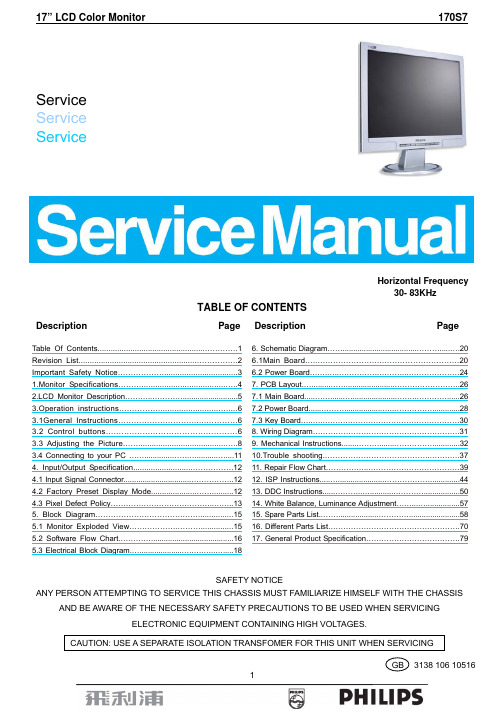
WARNING
Use of substitute replacement parts, which do not have the same, specified safety characteristics may create shock, fire, or other hazards. Uhould the original design be modified or altered without written permission from Philips. Philips assumes no liability, express or implied, arising out of any unauthorized modification of design. Servicer assumes all liability. FOR PRODUCTS CONTAINING LASER: DANGER-Invisible laser radiation when open. AVOID DIRECT EXPOSURE TO BEAM. CAUTION-Use of controls or adjustments or performance of procedures other than those specified herein may result in hazardous radiation exposure. CAUTION -The use of optical instruments with this product will increase eye hazard. TO ENSURE THE CONTINUED RELIABILITY OF THIS PRODUCT, USE ONLY ORIGINAL MANUFACTURER'S REPLACEMENT PARTS, WHICH ARE LISTED WITH THEIR PART NUMBERS IN THE PARTS LIST SECTION OF THIS SERVICE MANUAL. Take care during handling the LCD module with backlight unit -Must mount the module using mounting holes arranged in four corners. -Do not press on the panel, edge of the frame strongly or electric shock as this will result in damage to the screen. -Do not scratch or press on the panel with any sharp objects, such as pencil or pen as this may result in damage to the panel. -Protect the module from the ESD as it may damage the electronic circuit (C-MOS). -Make certain that treatment person’s body is grounded through wristband. -Do not leave the module in high temperature and in areas of high humidity for a long time. -Avoid contact with water as it may a short circuit within the module. -If the surface of panel becomes dirty, please wipe it off with a soft material. (Cleaning with a dirty or rough cloth may damage the panel.)
Philips 107S76 数字化真实平面 CRT 显示屏说明书
PhilipsCRT monitor43 cm (17")real flatXGA107S76digitalized Real-Flat CRT, viewing ease and valuewith lead-free designWith a Digital Deflection CPU, one-touch brightness enhancement, high brightness RealFlat CRT tube and ideal screen size, the 107S7 delivers an unbeatable mix of performanceand value plus environment-friendly lead-free design.Outstanding front of screen performance•Philips breakthrough advanced Digital Deflection CPU•High Bright Hot Key instantly adjusts brightness levels•XGA 1024x768 resolution for sharper display•Real flat CRT for natural, distortion and glare-free display•Easy-on-the-eyes high-bright, high-contrast tube•sRGB ensures color matching between display and printoutsGreat convenience•Compatibility with PC and Mac platforms•Easy, user friendly plug-and-play installationGreen design•Lower power consumption than the industry average•MPRII ensures safety by limiting electromagnetic radiation•For your safety: Aerospace composite fire retardant caseHighlightsDigital Deflection CPUAn exclusive Philips innovation -- the world's first one-chip CRT solution -- combines the deflection and the Microcontroller in a single chip to process and control input sync digitally. This innovative technology prevents electronic noise that can harm display quality, reduces display jitter and improves geometry for better front of screen performance.High Bright Hot KeyA feature that delivers instant brightness adjustment to the ideal level for viewing text, Internet, game or multimedia applications, providing comfortable viewing and an enhanced experience for each type of application.XGA, 1024 x 768 resolutionFor graphics monitors, the screen resolution signifies the number of dots (pixels) on the entire screen. For example, a 1024-by-768 pixel screen is capable of displaying 1024 distinct dots on each of 768 lines, or about 786 thousand pixels. XGA provides resolutions of640 by 480 or 1024 by 768 pixels.Real flat CRT displayPhilips advanced flat CRT technology reducesglare and reflection more efficiently than aconventional CRT. The special high-bright,high-contrast shadow mask helps maintainsharper focus and eliminates 'color blooming'compared to standard tubes. It displays imageson a monitor that look like images on paper:Viewing the image is more comfortable.Straight lines are straight. Finding a reflection-free viewing position is much easier. This addsup to reduced eyestrain for a comfortableviewing experience.High-bright-high-contrast tubeA CRT tube designed to increase displaybrightness and contrast by increasing the CRTray gun's beam current.sRGB readysRGB is an industry standard that ensures thebest possible match between the colorsdisplayed on your screen and those in yourprintouts.Two-platform compatibilityThe ability to work with a variety of platforms;Philips monitors are compatible to connectwith PC by employing a VGA connection andconnect with Macintosh.Energy efficiencyReduction of the electrical power required tooperate a device to achieve real savings.MPRII compliantThe world standard setting stringent levels forelectromagnetic radiation emitted bymonitors.Flame retardant cabinetPC/ABS plastic composite is the industry's bestand toughest flame-retardant casing material;and is a space-age compound deployed in theaerospace and automotive industries as well asin fire detectors that is compliant with moststringent fire safety standards.Issue date 2021-02-16 Version: 1.0.212 NC: 8639 000 17088 EAN: 87 10895 97266 6© 2021 Koninklijke Philips N.V.All Rights reserved.Specifications are subject to change without notice. Trademarks are the property of Koninklijke Philips N.V. or their respective owners.SpecificationsPicture/Display•Display screen type: Real Flat picture tube •Panel Size: 17"/ 41 cm•Phosphor: P22•Recommended display area(mm): 306 x 230 mm •Recommended Display Area(inch): 12" x 9"•Dot pitch: 0.25 mm•Dot Pitch (horizontal): 0.21 mm•White Chromaticity, 6500K: x = 0.313 / y = 0.329•White Chromaticity, 9300K: x = 0.283 / y = 0.297•Maximum Resolution: 1280 x 1024 @ 60 Hz •Optimum resolution: 1024 x 768 @ 85 Hz •Factory Preset Modes: 8 modes•Factory Preset Mode: 640 x 480 @ 60 Hz, 640 x 480 @ 85Hz, 720 x 400 @ 70 Hz, 800 x 600 @ 75 Hz, 800 x 600 @ 85 Hz, 1024 x 768 @ 75 Hz, 1024 x 768 @ 85 Hz, 1280 x 1024 @ 60 Hz •Factory Preload Modes: 10 modes•Video Dot Rate: 110 MHz•Horizontal Scanning Frequency: 30 - 71 kHz •Vertical Scanning Frequency: 50 - 160 Hz •Recommended Refresh Rate: 85 Hz•Screen enhancement: Anti-glare Polarizer, Anti-Reflection, Anti-Static, High Brightness, High Contrast•Digital deflection•sRGB•GTFConnectivity•Cables: D-sub Video Cable, Power Cord •Cable Connection: AC Power in•Sync input impedance: 2.2k ohm•Video input impedance: 75 ohm•Video input signal levels: 0.7 Vpp•Sync Input: Separate Sync•Video Sync Polarities: Positive and Negative Convenience•User convenience: Menu Languages, On-screen Display •Monitor Controls: Bright Direct Access, Contrast Direct Access, High Bright Hotkey, Menu, Power On/Off•OSD Languages: English, French, German, Italian, Korean, Portuguese, Spanish, Simplified Chinese •Plug & Play Compatibility: DDC 2B, Windows 98/ ME/2000/XP•Regulatory approvals: BSMI, CCC, CE Mark, C-Tick, DHS, eK, FCC-B, UL, CSA, FDA, GOST, IRAM, MIC, MPR-II, Low Emission, NOM, PSB, SEMKO, TÜV/GS, TÜV Ergo•Swivel:+/-90°•Tilt: -5° to 13°Accessories•Included accessories: AC Power Cord•User ManualDimensions•Box dimensions(W x H x D):446 x 420 x 475 mm•Box dimensions in inch (W x H x D):17.6 x 16.5 x 18.7 inch•Set dimensions(W x H x D):397 x 382 x 423.5 mm•Set dimensions in inch (W x H x D):15.6 x 15 x 16.7 inch•Set weight: 13.5 kg•Set weight (lb): 29.7 lb•Weight incl. Packaging: 15.4 kg•Weight incl. Packaging (lb): 33.95•Temperature range (operation): 0°C to 40°C •Temperature range (storage): -25°C to 65°C Power•Consumption(On mode): 62 W (Typical)•Consumption (Off Mode): around 1 W •Power LED indicator: Off - Flashing Green, Operation - green•Power supply: Built-in, 100-264 VAC, 50/60 Hz。
AOPEN 液晶显示器快速入门指南(QSG)说明书
用螺丝刀转动黑色螺丝,将其固定。 将支架臂固定到显示器上。
HDMI/DP HDMI/DP
注:使用HDMI缆线的,显示器刷新率可达144Hz; 使用DP缆线的,显示器刷新率可达165Hz;
适配器 电源线
1 2 3 4 5
适配器
HDMI DP
进入主菜单。 进入信源模式。 进入 切换模式菜单。 进入 亮度调节 。 开/关机。
内页
来料折叠方式:
基本内容 销往地
BOM /批次
中国
印刷内容见下页
制作会签
2019-11-21
业务/DQA
会
签
HC5 Series
32HC5QR
外页
AOPEN 液晶显示器快速入门指南 (QSG) 电源适配器
电源适配器 AOPEN
电源适配器
螺丝刀 黑色
资料更新履历
TCL多媒体 SCBC(战略客户业务中心) 设计中心-平面设计室
平面设计制作规范表
物料编码 物料名称
70-EK320Q-QSGZ2 QSG快速安装指南
品牌 机型/机芯 销售型号
制作要求
工艺或使用方法
尺寸
420x300mm
材质
80G普通书纸
颜色
要求
黑白印刷
是否折 叠或装 订要求
折叠
是否送样 是 备注:
- 1、下载文档前请自行甄别文档内容的完整性,平台不提供额外的编辑、内容补充、找答案等附加服务。
- 2、"仅部分预览"的文档,不可在线预览部分如存在完整性等问题,可反馈申请退款(可完整预览的文档不适用该条件!)。
- 3、如文档侵犯您的权益,请联系客服反馈,我们会尽快为您处理(人工客服工作时间:9:00-18:30)。
CHIMEI INNO L U X DISPLAY CORPORATIONLCD MODULESPECIFICATIONCustomer: Model Name: ZJ070NA-01PDate: 2012/01/11 Version:01■Preliminary Specification □Final SpecificationFor Customer ’s AcceptanceApproved byCommentApproved byReviewed byPrepared byCharlie Chou2012/02/01Wenyi Wang2012/02/01David Lee2012/01/31深显实业有限公司 CHIMEI InnoLux copyright2004All rights reserved,Copying forbidden. Record of RevisionVersion ReviseDatePage ContentPre-Spec.01 2012/01/11 Initial Release.CHIMEI INNO L U XContents1. General Specifications (1)2. Pin Assignment (2)3. Operation Specifications (5)3.1. Absolute Maximum Ratings (5)3.1.1. Typical Operation Conditions (6)3.1.2. Current Consumption (7)3.1.3. Backlight Driving Conditions (7)3.2. Power Sequence (8)3.3. Timing Characteristics (9)3.3.1. AC Electrical Characteristics (9)3.3.2. Input Clock and Data Timing Diagram (9)3.3.3. DC Electrical Characteristics (10)3.3.4. Timing (11)3.3.5. Data Input Format (12)4. Optical Specifications (13)5. Reliability Test Items (17)6. General Precautions (18)6.1. Safety (18)6.2. Handling (18)6.3. Static Electricity (18)6.4. Storage (18)6.5. Cleaning (18)7. Mechanical Drawing (19)8. Package Drawing (20)8.1. Packaging Material Table (20)8.2. Packaging Quantity (20)8.3. Packaging Drawing (21)1. General SpecificationsNo. Item Specification Remark1 LCD size 7.0 inch(Diagonal)2 Driver element a-Si TFT active matrix3 Resolution 1024 × 3(RGB) × 6004 Display mode Normally White, Transmissive5 Dot pitch 0.05(W) × 0.15(H) mm6 Active area 153.6(W) × 90.0(H) mm7 Module size 165.75 (W) ×105.39(H) ×4.8(D) mm Note 18 Surface treatment Glare9 Color arrangement RGB-stripe10 Interface Digital11 View direction(Gray Inversion) 6 O’Clock12 Backlight power consumption 3.564W (Typ.)13 Panel power consumption 0.35W (Typ.)14 Weight TBD(Typ.)Note 1: Refer to Mechanical Drawing.2. Pin AssignmentFPC Connector is used for the module electronics interface. The recommended model is FH12A-40S-0.5SH manufactured by Hirose.Pin No. Symbol I/O Function Remark1 VCOM P Common Voltage2 VDD P Power Voltage for digital circuit3 VDD P Power Voltage for digital circuit4 NC --- No connection5 Reset I Global reset pin6 STBYB I Standby mode, Normally pulled high STBYB = “1”, normal operation STBYB = “0”, timing controller, source driver will turn off, all output are High-Z7 GND P Ground8 RXIN0- I - LVDS differential data input9 RXIN0+ I + LVDS differential data input10 GND P Ground11 RXIN1- I - LVDS differential data input12 RXIN1+ I + LVDS differential data input13 GND P Ground14 RXIN2- I - LVDS differential data input15 RXIN2+ I + LVDS differential data input16 GND P Ground17 RXCLKIN- I - LVDS differential clock input18 RXCLKIN+ I + LVDS differential clock input19 GND P Ground20 RXIN3- I - LVDS differential data input21 RXIN3+ I + LVDS differential data input22 GND P Ground23 NC --- No connection24 NC --- No connection25 GND P Ground26 NC --- No connection27 DIMO O Backlight CABC controller signal output28 SELB I 6bit/8bit mode select Note129 AVDD P Power for Analog Circuit30 GND P Ground31 LED- P LED Cathode32 LED- P LED Cathode33 L/R I Horizontal inversion Note334 U/D I Vertical inversion Note335 VGL P Gate OFF Voltage36 CABCEN1 I CABC H/W enable Note237 CABCEN0 I CABC H/W enable Note238 VGH P Gate ON Voltage39 LED+ P LED Anode40 LED+ P LED AnodeI: input, O: output, P: PowerNote1: If LVDS input data is 6 bits ,SELB must be set to High;If LVDS input data is 8 bits ,SELB must be set to Low.Note2: When CABC_EN=”00”, CABC OFF.When CABC_EN=”01”, user interface image.When CABC_EN=”10”, still picture.When CABC_EN=”11”, moving image.When CABC off, don’t connect DIMO, else connect it to backlight. Note3: When L/R=”0”, set right to left scan direction.When L/R=”1”, set left to right scan direction.When U/D=”0”, set top to bottom scan direction.When U/D=”1”, set bottom to top scan direction.Note: Definition of scanning direction.Refer to the figure as below:3. Operation Specifications3.1. Absolute Maximum Ratings(Note 1)ValuesUnit Remark Item SymbolMin. Max.DV DD -0.3 5.0 VAV DD 6.5 13.5 V Power voltageV GH -0.3 42.0 VV GL -20.0 0.3 VV GH-V GL- 40.0 V Operation Temperature T OP -30 80 ℃Storage Temperature T ST-30 80 ℃LED Reverse Voltage V R- 5 VEach LED LED Forward Current I F- 60 mA Each LEDNote 1: The absolute maximum rating values of this product are not allowed to be exceeded at any times. Should a module be used with any of the absolute maximum ratingsexceeded, the characteristics of the module may not be recovered, or in an extremecase, the module may be permanently destroyed.3.1.1. Typical Operation Conditions( Note 1)ValuesUnit Remark Item SymbolMin. Typ. Max.DV DD 3.0 3.3 3.6 V Note 2AV DD 10.8 11 11.2 VPower voltageV GH 19.7 20 20.3 VV GL -6.5 -6.8 -7.1 VInput signal voltage V COM 2.7 (3.7) 4.7 V Note 4Input logic high voltage V IH 0.7 DV DD - DV DD VNote 3 Input logic low voltage V IL 0 - 0.3 DV DD VNote 1: Be sure to apply DV DD and V GL to the LCD first, and then apply V GH.Note 2: DV DD setting should match the signals output voltage (refer to Note 3) of customer’s system board.Note 3: LVDS,Reset.Note 4: Typ. V COM is only a reference value, it must be optimized according to each LCM.Be sure to use VR;3.1.2. Current ConsumptionValuesItem SymbolMin. Typ. Max.Unit RemarkI GH - 0.25 1.0 mA V GH =20VI GL - 0.25 1.0 mA V GL = -6.8V IDV DD - 38 60 mA DV DD =3.3VCurrent for DriverIAV DD - 20 30 mA AV DD =11V3.1.3. Backlight Driving ConditionsValuesItem SymbolMin. Typ. Max.Unit Remark Voltage for LED backlight V L -- 9.9 10.5 V Note 1 Current for LED backlight I L -- 360 420 mALED life time - - 20,000 - Hr Note 2Note 1: The LED Supply Voltage is defined by the number of LED at Ta=25℃ andI L =360mA.Note 2: The “LED life time” is defined as the module brightness decrease to 50% original brightness at Ta=25℃ and I L =360mA. The LED lifetime could be decreased ifoperating I L is lager than 360mA.3.2. Power Sequencea. Power on:b. Power off:VDD STBYB RESET A VGL VGH LVDS Signal B/L >50ms>=0ms>100ms>=0msNormal signal VCOM <20ms VDD STBYB RESET A VGL VGH LVDS SignalB/L >120ms>50us>40us>20us <20ms<500us >500usNormal signalVCOM >35ms3.3. Timing Characteristics3.3.1. AC Electrical CharacteristicsValuesParameter SymbolUnit RemarkMin. Typ. Max.Clock frequency R xFCLK40.8 51.2 67.2 MHzInput data skew margin T RSKM500 - - psClock high time T LVCH- 4/(7* R xFCLK) - nsClock low time T LVCL- 3/(7* R xFCLK) - ns3.3.2. Input Clock and Data Timing Diagram3.3.3. DC Electrical CharacteristicsValuesParameter SymbolMin. Typ. Max.Unit RemarkDifferential input highThreshold voltageR xVTH- - +0.1 VDifferential input low Threshold voltage R xVTL-0.1 - - VR XVCM=1.2VInput voltage range(singled-end)R xVIN0 - 2.4 V Differential input common modevoltageR xVCM|V ID|/2 - 2.4-|V ID|/2 V Differential voltage|V ID|0.2 - 0.6 V Differential input leakage current RV xliz-10 - +10 uA3.3.4. TimingValuesItem SymbolMin. Typ. Max.Unit RemarkClock Frequency fclk 40.8 51.2 67.2 MHz Frame rate =60HzHorizontal display area thd1024 DCLK HS period time th1114 1344 1400 DCLK HS Blanking thb90 320 376 DCLK Vertical display area tvd600 H VS period time tv610 635 800 H VS Blanking thb10 35 200 H3.3.5. Data Input Format6bit LVDS input8bit LVDS inputNote: Support DE timing mode only, SYNC mode not supported.4. Optical SpecificationsValuesItemSymbolConditionMin.Typ. Max. UnitRemarkθLΦ=180°(9 o’clock) 65 75 - θR Φ=0°(3 o’clock) 65 75 -θT Φ=90°(12 o’clock) 60 70 - Viewing angle (CR≥ 10)θB Φ=270°(6 o’clock)65 75 - degree Note 1 T ON-1020msecNote 3Response timeT OFF- 15 30 msec Note 3 Contrast ratioCR 500 700 - - Note 4 W X0.26 0.31 0.36 - Color chromaticityW Y0.28 0.33 0.38 - Note 2 Note 5 Note 6 LuminanceL400500-cd/m²Note 6LuminanceuniformityY U Normal θ=Φ=0°70 75 - % Note 7Test Conditions:1. DV DD =3.3V, I L =360mA (Backlight current), the ambient temperature is 25℃.2. The test systems refer to Note 2.Fig. 4-1 Definition of viewing angleNote 2: Definition of optical measurement system.The optical characteristics should be measured in dark room. After 30 minutesoperation, the optical properties are measured at the center point of the LCD screen. (Response time is measured by Photo detector TOPCON BM-7, other items are measured by BM-5A/Field of view: 1° /Height: 500mm.)Fig. 4-2 Optical measurement system setupNormal line θ=Φ=0°Photo detectorΦ=90°12 o’clock directionΦ=270°6 o’clock directionΦ=0°Φ=180°Active Area500mmLCMθ=Φ=0°Φ=90°12 o’clock direction Φ=270°6 o’clock direction Φ=0°Φ=180°Active AreaθLθTθBθRLCMNote 3: Definition of Response timeThe response time is defined as the LCD optical switching time interval between“White” state and “Black” state. Rise time (T ON ) is the time between photo detector output intensity changed from 90% to 10%. And fall time (T OFF ) is the time between photo detector output intensity changed from 10% to 90%.Fig. 4-3 Definition of response timeNote 4: Definition of contrast ratiostate Black"" the on LCD when measured Luminance state White"" the on LCD when measured Luminance (CR) ratio Contrast =Note 5: Definition of color chromaticity (CIE1931)Color coordinates measured at center point of LCD.Note 6: Definition of luminance:Measured at the center area of the panel when LCD panel is driven at “white ” state. The LED driving condition is I L =360mA .90%10% 0%P h o t o d e t e c t o r o u t p u t (R e l a t i v e v a l u e )ONT White (TFT OFF)Black (TFT ON)White (TFT OFF)Note 7: Definition of Luminance UniformityActive area is divided into 9 measuring areas (Refer to Fig. 4-4 ).Every measuring point is placed at the center of each measuring area.max minB B (Yu)Uniformity Luminance =L-------Active area length W----- Active area widthWW /3W /3W /6L/3L/3L/6LFig. 4-4 Definition of measuring pointsB max : The measured maximum luminance of all measurement position. B min : The measured minimum luminance of all measurement position.5. Reliability Test Items(Note3)Item Test Conditions Remark High Temperature Storage Ta = 80℃240hrs Note 1,Note 4 Low Temperature Storage Ta = -30℃240hrs Note 1,Note 4 High Temperature Operation Ts = 80℃240hrs Note 2,Note 4 Low Temperature Operation Ta = -30℃240hrs Note 1,Note 4 Operate at High Temperatureand Humidity+60℃, 90%RH 240hrs Note 4Thermal Shock -30℃/30 min ~ +80℃/30 min for a total 100cycles, Start with cold temperature and endwith high temperature.Note 4Vibration Test Frequency range:10~55Hz Stroke:1.5mmSweep:10Hz~55Hz~10Hz2 hours for each direction of X. Y. Z.(6 hours for total)Mechanical Shock 100G 6ms,±X, ±Y, ±Z 3 times for each directionPackage Vibration Test Random Vibration :0.015G*G/Hz from 5-100HZ, -6dB/Octave from 100-200HZ2 hours for each direction of X. Y. Z.(6 hours for total)Package Drop Test Height:60 cm1 corner, 3 edges, 6 surfacesElectro Static Discharge ± 2KV, Human Body Mode, 100pF/1500ΩNote 1: Ta is the ambient temperature of samples.Note 2: Ts is the temperature of panel’s surface.Note 3: In the standard condition, there shall be no practical problem that may affect the display function. After the reliability test, the product only guarantees operation,but don’t guarantee all of the cosmetic specification.Note 4: Before cosmetic and function test, the product must have enough recovery time, at least 2 hours at room temperature.6. General Precautions6.1. SafetyLiquid crystal is poisonous. Do not put it in your mouth. If liquid crystal touches your skin or clothes, wash it off immediately by using soap and water.6.2. Handling1. The LCD panel is plate glass. Do not subject the panel to mechanical shock or toexcessive force on its surface.2. The polarizer attached to the display is easily damaged. Please handle it carefullyto avoid scratch or other damages.3. To avoid contamination on the display surface, do not touch the module surfacewith bare hands.4. Keep a space so that the LCD panels do not touch other components.5. Put cover board such as acrylic board on the surface of LCD panel to protect panelfrom damages.6. Transparent electrodes may be disconnected if you use the LCD panel underenvironmental conditions where the condensation of dew occurs.7. Do not leave module in direct sunlight to avoid malfunction of the ICs.6.3. Static Electricity1. Be sure to ground module before turning on power or operating module.2. Do not apply voltage which exceeds the absolute maximum rating value.6.4. Storage1. Store the module in a dark room where must keep at 25±10℃ and 65%RH or less.2. Do not store the module in surroundings containing organic solvent or corrosivegas.3. Store the module in an anti-electrostatic container or bag.6.5. Cleaning1. Do not wipe the polarizer with dry cloth. It might cause scratch.2. Only use a soft sloth with IPA to wipe the polarizer, other chemicals mightpermanent damage to the polarizer.7. Mechanical Drawing深显实业有限公司8. Package Drawing8.1. Packaging Material TableNo. ItemModel(Material)Dimensions(mm)UnitWeight(kg)Quantity Remark1 LCMModuleZJ070NA-01P 165.75 × 105.39 × 4.8 TBD TBD2 Partition BC CorrugatedpaperTBD TBD 1set3 CorrugatedPaperB CorrugatedpaperTBD TBD 4pcs4 CorrugatedBarB CorrugatedpaperTBD TBD 4pcs5 Dust-ProofBagPE 700 × 530 0.048 1pcs6 A/S Bag PE 180 × 133 × 0.2 0.002 50pcs7 Carton Corrugatedpaper530 × 355 × 255 1.100 1pcs8 Total weight TBD8.2. Packaging QuantityTotal LCM quantity in Carton: no. of Partition TBD Rows × quantity per Row TBD = TBD8.3. Packaging Drawing TBD。