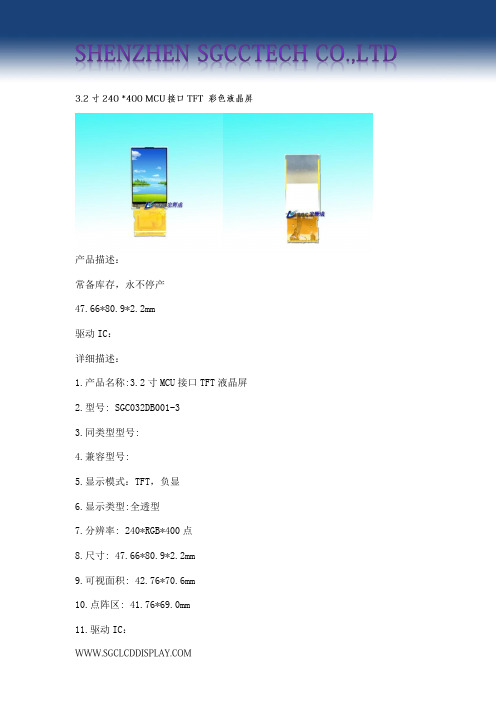
3.2寸TFT液晶规格书
3.2寸240 400 MCU接口TFT液晶屏
存储的防范措施(Storage Precautions) 10.2.1 储存液晶显示模块时,要避免受到阳光的直射或荧光灯的光。 10.2.2 液晶显示模块应存储在存储温度范围。如果液晶显示模块将被存放很长 一段时间,推荐条件是:温度:0℃~40℃ 相对湿度:≤80% 10.2.3 液晶显示模块,应存放在无酸、碱及有害气体的房间。
12.接口类型:16/18 位 MCU 并联接口模式 13.连接类型:焊接型 14.背光灯颜色及类型:白色 LED 并联 15.可视角度: 12:00 16.工作温度: -20----70℃ degrees 17.储存温度: -30----80℃ degrees 操作注意事项 1.1 显示面板是玻璃做成的。不要让它从高的地方下跌受到机械冲击,等等。 1.2 如果显示面板损坏了和液晶物质里面泄漏出来,嘴里一定要没有任何的物质, 如果您的皮肤或衣服接触到了,及时用肥皂和水洗掉。 1.3 不要对显示器表面或邻近地区用力过猛,因为这可能会导致色调的改变。 1.4 覆盖在液晶显示模块显示表面的偏光板是软的,容易划伤。仔细处理这个偏 光片。 1.5 如果显示器表面被污染,将气吹在其表面上,并用柔软的干布轻轻擦拭。如 果仍然没有完全清除,用下列溶剂之一来湿润布: -异丙醇 -乙醇 用除上述以外的溶剂可能会损坏偏光板。尤其是,不要使用以下: -水 -酮 -芳烃溶剂 1.6 不要尝试拆解液晶显示模块。 1.7 如果逻辑电路的电源是关闭的,不适合用输入信号。 1.8 为了防止静电破坏元素,要小心保持最佳的工作环境。
3寸屏(240X400)规格书
SLT3001DDisplay Module SPECIFICATION Customer:Customer NO.:Approved By :For Solution ---3.0 inch ;240(H) X RGB X 400(V)Owner:Version: V1Document ID:SLT3001DCopyright © STAR Corporation. This material, including documentation and any related computer programs, is protected by copyright controlled byWinstar Corporation. All rights are reserved. Copying, including reproducing,storing, adapting or translating, any or all of this material requires the priorwritten consent of Winstar Corporation. This material also containsconfidential information, which may not be disclosed to others without theprior written consent of STAR Corporation.Approved byTable of contents1. Features2. Change History3. Block Diagram4. Interface specifications5 MPU and LCM connection format (System Interface Block)6. Timing Characteristics7. Mechanical Specifications8. Electrical Specifications9. Optical characteristics10. QUALITY AND RELIABILITY11. USE PRECAUTIONS12. OUTLINE DIMENSION1. FeaturesMain LCD 3.0 inch a-Si--TFT--LCD (Thin Film Transistor Liquid Crystal Display) for mobile-phone or handy electrical equipments.1.1 Construction: 3.0” a-Si color TFT-LCD with White LED Backlight.1.2Main LCD :1.2.1 Amorphous-TFT3.0 inch display, transmissive, Normally white type, 12 o’clock.1.2.2 240(RGB)X400 dots Matrix.1.2.3 LCD controller is SPFD5420A or Equivalent.1.2.4 Real 262K colors display Red-6bit, Green-6bit, Blue-6bit(18-bit 8080 interface); 65K: Red-5bit, Green-6bit, Blue-5bit (16-bit 8080 interface)2. Change History:(Detail)3. Block Diagram MPU TO Connect LCM Format4. Interface specificationsItem Terminal Functions1 LCM_ID NC2 XL Touch Panel Onput PIN3 YU Touch Panel Onput PIN4 XR Touch Panel Onput PIN5 YD Touch Panel Onput PIN6 GND Ground7 IOVCC Power input(1.8V/2.8V)8 VCC/VCI Power input(2.8V)9 FARMK NC10 CS Chip Select Input PIN11 RS Register Select Input PIN12 WR Write Data Select Input PIN13 RD Read Data Select Input PIN14-29 DB0-DB15 Input/output data pin16 bit: DB0---DB158 bit: DB8—DB15 //高8位30 RESET Chip reset Select Input PIN31 GND Ground32 A B/L Power input PIN anode33-36 K1-K4 B/L Power input PIN negative37 NC NC5 System Interface Block6. Timing Characteristics80-system Bus interface Timing Characteristics (Main LCD)7. Mechanical Specifications7.1 Dimensions and weightItem Specifications Unit External shape dimensions *45.04 (W) x77(H) x 3.4MAX) mmMain LCD Pixel Pitch 54x162 um Active Area 38.88(W) x 64.8(H) mmWeight TBD g*1. This specification is about External shape on shipment from Winstar7.2 Absolute max. ratings and environment7.2.1 Absolute max. ratingsTa=25oC GND=0V Item Symbol Min. Max. Unit Remarks Power Supply for Logic VCC-GND -0.3 +4.6 VPower Supply for LED backlight LEDA-LEDK -0.5 +5 VInput voltage VIN -0.5 VCC+0.5 V7.2.2 EnvironmentItem Specification Remarks Storage temperature Max. +70 ℃, Min. –30℃Note 1: Non-condensing Operating temperature Max. +60 ℃, Min. -20℃Note 1: Non-condensingNote 1:Ta≦+40℃・・・・Max.85%RHTa>+40℃・・・・The max. humidity should not exceed the humidity with 40℃85%RH.8. Electrical Specifications8.1 Electrical characteristics of LCD8.2 LED back light specificationItem Symbol Conditions MIN. TYP. MAX. Unit Forward voltage Vf If =60mA -- 3.3 3.5 V Reverse voltage Vr -- -- 5.0 V Forward current If 4-chip Parallel -- 60 80 mA Power Consumption PBL f =60mA -- 192 280 mW Uniformity (with L/G) -- If=60mA 80% *1 -- -- Luminous color WhiteChip connection 4 chip Parallel connection9. Optical characteristics9.1 LED backlight transmissive module:Item Symbol Temp. Min. Typ. Max. Unit ConditionResponse Time Tr 25℃-- 10 --ms θ=0 °,φ=0 ° (Note 2) Tf 25℃-- 15 --Contrast Rate Cr 25℃100 350 -- -- θ=0 °, φ=0 °LED:ON, LIGHT:OFF(Note 4)Transmittance T 25℃-- 5.0 -- ℅Visual anglerange front and rear θ25℃(θf) 60(θb)55De-greeφ= 0°, CR≧10 LED:ONLIGHT:OFF(Note 3)Visual anglerange left andright θ25℃(θl) 50(θr) 50De-greeφ=90°, CR≧10 LED:ONLIGHT:OFF(Note 3)Visual angledirectionpriority12:00 (Note 5)Brightness 150 Cd/m2 ILED=15mA Full Whitepattern9.2 Main LCD(Only Panel): (Ta = 25℃)9.3 BackLightItem Symbol TransmissiveConditionsMin. Typ. Max.Light Source 0.26 0.28 Note 1 0.26 0.2810. QUALITY AND RELIABILITY10.1 TEST CONDITIONSTests should be conducted under the following conditions:Ambient temperature: 25 ± 5°CHumidity : 60 ± 25% RH.10.2 SAMPLING PLANSampling method shall be in accordance with MIL-STD-105E , level II, normal single sampling plan .10.3 ACCEPTABLE QUALITY LEVELA major defect is defined as one that could cause failure to or materiallyreduce the usability of the unit for its intended purpose. A minor defect is one that does not materially reduce the usability of the unit for its intended purpose or is an infringement from established standards and has no significant bearing on its effective use or operation.10.4 APPEARANCEAn appearance test should be conducted by human sight at approximately 30 cm distance from the LCD module under fluorescent light. The inspection area of LCD panel shall be within the range of following limits.10.5 INSPECTION QUALITY CRITERIA10.6 RELIABILITYInspection Item Criteria and Description Defect typeVertical line Signal input, vertical line off or irregular V-lineappearsmajorHorizontal line Signal input, horizontal line off or irregular H-lineappearsmajorCross line Pattern signal input, a correct display is not obtained major No display Signal input, display is dead major Irregular display Pattern signal input, a correct display is not obtained major Dots defect Exceed specified standards minor Foreign material Exceed specified standards minorMura It's OK if mura is slight visible through 6%ND filter. (Judged by limit sample if it is necessary)minorExternal Appearance A appearance defect that do not affect function or performanceminorPanelcrack/broken/burrExceed specified standards major 10.7 RELIABILITYTest Item Test Conditions Notes High temperature Operation 60±3℃,T=96hrsLow temperature Operation -20±3℃,T=96hrsHigh Temperature Storage 70±3℃,T=96hrs1,2 Low Temperature Storage -20±3℃,T=96hrs1,2 Humidity Test 40℃,Humidity 90% ,96hrs1,2Thermal Shock Test -30℃〜25℃〜80℃,30min 5min 30min(1 cycle)Total 5 cycle1,2Vibration Test(Packing) Sweep frequency 10〜55〜10HZ/minAmplitude:0.75mmTest direction:X,Y,Z/3 axis2Duration 30min/each axisStatic Electricity 150Pf 330ohm ±8KV, 10time air dischargeNote 1: Condensation of water is not permitted on the moduleNote 2: the module should be inspected after 1 hour storge in normalConditions(15〜35℃,45-65%RH).Definitions of life end point:●Current drain should be smaller than the specific value●Function of the module should be maintained●Appearance and display quality should not have degraded noticeably●Contrast ratio should be greater that 50% of the initial value11. USE PRECAUTIONS11.1 Handling precautions1) The polarizing plate may break easily so be careful when handling it. Do not touch, press or rub it with a hard-material tool like tweezers.2) Do not touch the polarizing plate surface with bare hands so as not to make it dirty. If the surface or other related part of the polarizing plate is dirty, soak a soft cotton cloth or chamois leather in benzene and wipe off with it. Do not use chemical liquids such as acetone, toluene and isopropyl alcohol. Failure to do so may bring chemical reaction phenomena and deteriorations.3) Remove any spit or water immediately. If it is left for hours, the suffered part may deform or decolorize.4) If the LCD element breaks and any LC stuff leaks, do not suck or lick it. Also if LC stuff is stuck on your skin or clothing, wash thoroughly with soap and water immediately.11.2 Installing precautions1) To prevent breaking by static electricity from the human body and clothing, earth the human body properly using the high resistance and discharge static electricity during the operation. In this case, however, the resistance value should be approx. 1MΩ and the resistance should be placed near the human body rather than the ground surface. When the indoor space is dry, static electricity may occur easily so be careful. We recommend the indoor space should be kept with humidity of 60% or more. When a soldering iron or other similar tool is used for assembly, be sure to earth it.2) When installing the module and ICs, do not bend or twist them. Failure to do so may crack LC element and cause circuit failure.3) To protect LC element, especially polarizing plate, use a transparent protective plate(e.g., acrylic plate, glass etc) for the product case.4) Do not use an adhesive like a both-side adhesive tape to make LCD surface (polarizing plate) and product case stick together. Failure to do so may cause the polarizing plate to peel off.11.3 Storage precautions1) Avoid a high temperature and humidity area. Keep the temperature between0°C and 35°C and also the humidity under 60%.2) Choose the dark spaces where the product is not exposed to direct sunlight or fluorescent light.3) Store the products as they are put in the boxes provided from us or in the same conditions as we recommend.11.4 Operating precautions1) Do not boost the applied drive voltage abnormally. Failure to do so may break ICs. When applying power voltage, check the electrical features beforehand and be careful. Always turn off the power to the LC module controller before removing or inserting the LC module input connector. If the input connector is removed or inserted while the power is turned on, the LC module internal circuit may break.2) The display response may be late if the operating temperature is under the normal standard, and the display may be out of order if it is above the normal standard. But this is not a failure; this will be restored if it is within the normal standard.3) The LCD contrast varies depending on the visual angle, ambient temperature, power voltage etc. Obtain the optimum contrast by adjusting the LC dive voltage.4) When carrying out the test, do not take the module out of the low-temperature space suddenly. Failure to do so will cause the module condensing, leading to malfunctions.5) Make certain that each signal noise level is within the standard (L level: 0.2Vdd or less andH level: 0.8Vdd or more) even if the module has functioned properly. If it is beyond the standard, the module may often malfunction. In addition, always connect the module when making noise level measurements.6) The CMOS ICs are incorporated in the module and the pull-up and pull-down function is not adopted for the input so avoid putting the input signal open while the power is ON.7) The characteristic of the semiconductor element changes when it is exposed to light emissions, therefore ICs on the LCD may malfunction if they receive light emissions. To prevent these malfunctions, design and assemble ICs so that they are shielded from light emissions.8) Crosstalk occurs because of characteristics of the LCD. In general, crosstalk occurs when the regularized display is maintained. Also, crosstalk is affected by the LC drive voltage. Design the contents of the display, considering crosstalk.11.5 Other1) Do not disassemble or take the LC module into pieces. The LC modules once disassembled or taken into pieces are not the guarantee articles.2) The residual image may exist if the same display pattern is shown for hours. This residual image, however, disappears when another display pattern is shown or the drive is interrupted and left for a while. But this is not a problem on reliability.11. OUTLINE DIMENSION。
320 340 TFT彩色LCD显示屏的多功能电力记录仪和数据记录仪操作手册说明书
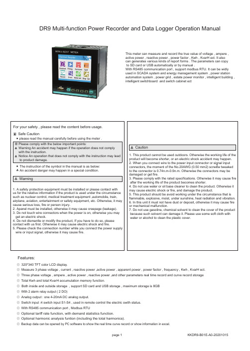
⊙ 320*340 TFT color LCD display.⊙ Measure 3 phase voltage , current , reactive power ,active power , apparent power , power factor , frequency , Kwh , KvarH ect.⊙ Three phase voltage , ampere , active power , reactive power ,and other parameters real time record and curve record storage ⊙ Total Kwh and total KvarH accumulation memory function .⊙ Both inside and outside storage , support SD card and USB storage , maximum storage is 8GB ⊙ With 2 alarm relay output ( 2 DO)⊙ Analog output : one 4-20mA DC analog output.⊙ Switch input :4 switch input S1-S4 , used in remote control the electric swith status.⊙ With RS485 communication port , Modbus RTU⊙ Optional tariff rate function, with demand statistics function.⊙ Optional harmonic analysis funtion (including the total harmonics).⊙ Backup data can be opened by PC software to show the real time curve record or show information in excel.Features:DR9 Multi-function Power Recorder and Data Logger Operation ManualThis meter can measure and record the true value of voltage , ampere , active power , reactive power , power factor , Kwh , KvarH ect. It also can generates various kinds of report forms . The parameters can copy to SD card or USB automatically or by manual .With RS485 communication port , support modbus RTU. It can be widly used in SCADA system and energy management system , power station automation system , power grid , estate power monitor , intelligent building ,intelligent switchboard and switch cabinet ectInstrument accessoriesPower Consumption ≤8VAFrequency 40~60Hz 、 Accuracy:0.1HzWorking Environment work temperature:-10℃~+45℃, Humidity <85%RH no condensation ,Work temperature limit:-25℃~+55℃, Storage temperature:-25℃~+70℃, Analog Output Alarm Output 4 On/Off output, 250VAC/3A or 30V DC/5A Dimension 96W×96H×100Lmminput VS power: AC 2000V, Power VS relay :AC 2000V ,Power VS transmition output:DC 2000V ,RS485 port ,isolated low voltage or I/O: DC 600VTechnical ParametersConnection 3 phase 3 wires, 3 phase 4 wiresVoltage Range AC 3x57.7V / 3X220V (note: Direct input volt: L-N: 0~600V, L-L: 0~1000V)Voltage Overload Continuous: 1.2 times Instantaneous: 2 times/10SVoltage Consumption <1VA (each phase)Voltage impedance ≥300KΩVoltage Accuracy RMS measurement , Accuracy : 0.5AC 0.025 ~ 5ACurrent Range Current Overload Continuous: 1.2 times Instantaneous: 4 times/10SCurrent Consumption <0.4VA (each phase)Current impedance <20m ΩCurrent Accuracy RMS measurement , Accuracy : 0.5Energy Active energy accuracy 0.5 / Reactive energy accuracy 1.Power Active power/Reactive power/Apparent power, accuracy: 0.5 Display TFT color display Power Supply AC/DC 100 ~ 240VOutput Digit InterfaceRS-485 Modbus-RTU Protocol1 transmition output, 4-20mA DC Load<400ΩAnti-jammingElectrostatic interference resistance ability :IEC61000-4-2,Level 2Radiation anti-jamming capacity: IEC61000-4-3,Level 3Fast transient pulse interface :IEC61000-4-4,Level 4Surge immunity (1,2/50us-8/20us ):IEC61000-4-5,Level 4Isolation&punctureInsulationInput/output/power supply to Meter cover >5MΩDimension and Mounting SizeSide size Hole sizeMake the lock button aim at adjustment screwA B CNCurrent input via CT A B CDO2AL2AC/DC DO1AL1POWER Wire ConnectionNote: 1. For voltage input connection terminal,bracket terminals (Ua) (Uc) (Ub) shows 3 phase 3 wire connection method, 2. Current input is current input terminal ,all the inputs and outputs must be coherentModel 1: (3pcs CT) 3 phase 4 wire working modeModel 2: (2pcs CT): 3 phase 3 wire working mode Current inputVoltage inputVoltage direct inputVoltage input via PTCurrent inputCurrent input via CT Voltage inputVoltage direct inputVoltage input via PTExplanation :A. Voltage input: Input voltage should not be higher than the rated input voltage of meter, otherwise a PT should be used.B. Current input: Standard rated input current is 5A. A CT should be used when the input current is bigger than 5A. If some other meters are connected with the same CT , the connection should be serial for all meters.C. Please make sure that the input voltage is corresponding to the input current, they should have the same phase sequence and direction,otherwise data and sign error may occur (power and energy).D. The connection mode of meter which is connected to power network should depend on the CT quantity. For 2pcs of CT, it should be 3 phase 3 wire connection. For 3pcs of CT, it shoud be 3 phase 4 wire connection.E. Please pay high attention on the difference between 3 phase 3 wire and 3 phase 4 wire connection , becasue wrong connection may lead to incorrect calculation of power factor, power and energy .Panel IndicationUSB portSD cardPage Guide。
TFT-LCD Approval Specification N116BGE-E32 Ver 3.2 for acer
Doc. Number:□ Tentative Specification □ Preliminary Specification ▓ Approval SpecificationMODEL NO.: N116BGESUFFIX: E32Approved ByChecked ByPrepared By楊竣傑 2013-12-25 16:49:18 CST曹文彬 2013-12-24 15:52:05 CST劉建宏 2013-12-20 16:59:17 CSTCONTENTS1. GENERAL DESCRIPTION (5)1.1 OVERVIEW (5)1.2 GENERAL SPECIFICATI0NS (5)2. MECHANICAL SPECIFICATIONS (5)2.1 CONNECTOR TYPE (6)3. ABSOLUTE MAXIMUM RATINGS (6)3.1 ABSOLUTE RATINGS OF ENVIRONMENT (6)3.2 ELECTRICAL ABSOLUTE RATINGS (7)3.2.1 TFT LCD MODULE (7)4. ELECTRICAL SPECIFICATIONS (8)4.1 FUNCTION BLOCK DIAGRAM (8)4.2. INTERFACE CONNECTIONS (8)4.3 ELECTRICAL CHARACTERISTICS (10)4.3.1 LCD ELETRONICS SPECIFICATION (10)4.3.2 LED CONVERTER SPECIFICATION (12)4.3.3 BACKLIGHT UNIT (14)4.4 DISPLAY PORT INPUT SIGNAL TIMING SPECIFICATIONS (15)4.4.1 DISPLAY PORT INTERFACE (15)4.4.2 COLOR DATA INPUT ASSIGNMENT (16)4.5 DISPLAY TIMING SPECIFICATIONS (17)4.6 POWER ON/OFF SEQUENCE (18)5. OPTICAL CHARACTERISTICS (21)5.1 TEST CONDITIONS (21)5.2 OPTICAL SPECIFICATIONS (21)6. RELIABILITY TEST ITEM (24)7. PACKING (25)7.1 MODULE LABEL (25)7.2 CARTON (26)7.3 PALLET (27)7.4 UN-PACKAGING METHOD (28)8. PRECAUTIONS (29)8.1 HANDLING PRECAUTIONS (29)8.2 STORAGE PRECAUTIONS (29)8.3 OPERATION PRECAUTIONS (29)Appendix. EDID DATA STRUCTURE (30)Appendix. OUTLINE DRAWING (33)Appendix. SYSTEM COVER DESIGN NOTICE (35)Appendix. LCD MODULE HANDLING MANUAL (41)REVISION HISTORYVersion Date Page Description3.0 Oct. 29, 2013 All Approval Spec Ver.3.0 was first issued for Acer3.1 Nov.8, 2013 30~32 Modify EDID Data3.2 Dec.12, 2013 34 Modify 2D Drawing Model Label location1. GENERAL DESCRIPTION1.1 OVERVIEWN116BGE-E32 is a 11.6” (11.6” diagonal) TFT Liquid Crystal Display module with LED Backlight unit and30 pins eDP interface. This module supports 1366 x 768 HD mode and can display 262,144 colors. Theoptimum viewing angle is at 6 o’clock direction.1.2 GENERAL SPECIFICATI0NSItem Specification Unit Note Screen Size 11.6 diagonalDriver Element a-si TFT active matrix - - Pixel Number 1366 x R.G.B. x 768 pixel - Pixel Pitch 0.1875 (H) x 0.1875 (V) mm - Pixel Arrangement RGB vertical stripe - - Display Colors 262,144 color - Transmissive Mode Normally white - - Surface Treatment Hard coating (3H), Anti-Glare - - Color Gamma 45% NTSC typ Luminance, White 220(typ.) Cd/m2Power Consumption Total 2.646 W (Max.) @ cell 0.75W (Max.),BL 1.896 W (Max)(1)Note (1) The specified power consumption (with converter efficiency) is under the conditions at VCCS =3.3 V, fv = 60 Hz, LED_VCCS = Typ, fPWM = 200 Hz, Duty=100% and Ta = 25 ± 2 ºC, whereas mosaicpattern is displayed.2. MECHANICAL SPECIFICATIONSItem Min.Typ. Max. Unit NoteHorizontal (H) 267.5 268 268.5 mm Vertical (V) 157 157.5 158 mmVertical (V)with PCB & Bracket 167.4 167.9 168.4 mmModule SizeThickness (T) X.X XX 3.4 mm (1)(2)Horizontal 258.825 259.125 259.425 mmPolarizer AreaVertical 146.5 146.8 147.1 mmHorizontal 255.825 256.125 256.425 mmActive AreaVertical 143.7 144 144.3 mmCF 0.35 0.4 0.45 mmGlassThickness TFT 0.35 0.4 0.45 mmWeight - 200 210 gNote (1) Please refer to the attached drawings for more information of front and back outline dimensions. Note (2) Dimensions are measured by caliper.2.1 CONNECTOR TYPEPlease refer Appendix Outline Drawing for detail design.Connector Part No.: IPEX-20455-030E-12 User’s connector Part No: IPEX-20453-030T-033. ABSOLUTE MAXIMUM RATINGS3.1 ABSOLUTE RATINGS OF ENVIRONMENTValueItemSymbol Min. Max. Unit Note Storage TemperatureT ST -20 +60 ºC (1) Operating Ambient Temperature T OP+50ºC(1), (2)Note (1) (a) 90 %RH Max. (Ta < 40 ºC).(b) Wet-bulb temperature should be 39 ºC Max. (Ta < 40 ºC).(c) No condensation.Note (2) The temperature of panel surface should be 0 ºC min. and 60 ºC max.Pin1Pin303.2 ELECTRICAL ABSOLUTE RATINGS3.2.1 TFT LCD MODULEValueItem SymbolUnit NoteMin. Max.Power Supply Voltage VCCS -0.3 +4.0 V(1)Logic Input Voltage V IN-0.3 VCCS+0.3 VConverter Input Voltage LED_VCCS -0.3 26 V (1) Converter Control Signal Voltage LED_PWM, -0.3 4 V 1) Converter Control Signal Voltage LED_EN -0.3 4 V (1) Note (1) Stresses beyond those listed in above “ELECTRICAL ABSOLUTE RATINGS” may cause permanent damage to the device. Normal operation should be restricted to the conditionsdescribed in “ELECTRICAL CHARACTERISTICS”.4. ELECTRICAL SPECIFICATIONS4.2. INTERFACE CONNECTIONSPIN ASSIGNMENTPin Symbol DescriptionRemark1 NC No Connection (Reserved for LCD test)2 H_GND High Speed Ground3 NC No Connection (Reserved for LCD test)4 NC No Connection (Reserved for LCD test)5 H_GND High Speed Ground6 ML0- Complement Signal-Lane 07 ML0+ True Signal-Main Lane 08 H_GND High Speed Ground9 AUX+ True Signal-Auxiliary Channel10 AUX- Complement Signal-Auxiliary Channel 11 H_GND High Speed Ground12 VCCS Power Supply +3.3 V (typical) 13 VCCS Power Supply +3.3 V (typical)14 NC No Connection (Reserved for LCD test) 15 GND Ground 16 GND Ground17 HPD Hot Plug Detect 18 BL_GND BL Ground 19 BL_GND BL Ground 20 BL_GND BL Ground 21 BL_GND BL Ground22 LED_ENBL_Enable Signal of LED Converter 23 LED_PWMPWM Dimming Control Signal of LEDConverter24NC No Connection (Reserved for LCD test)SignalsConverter Input SignalsGND25 NC No Connection (Reserved for LCD test) 26 LED_VCCS BL Power 27 LED_VCCS BL Power 28 LED_VCCS BL Power29 LED_VCCSBL Power30NCNo Connection (Reserved for LCD test)Note (1) The first pixel is odd as shown in the following figure.4.3 ELECTRICAL CHARACTERISTICS4.3.1 LCD ELETRONICS SPECIFICATIONValueParameterSymbol Min. Typ. Max. UnitNote Power Supply Voltage VCCS 3.0 3.3 3.6 V(1) High Level - 2.25 - 2.75 V (4) HPDLow Level- 0 - 0.4 V (4) HPD Impedance R HPD 30K ohm (4) Ripple Voltage V RP - 50 - mV(1) Inrush Current I RUSH - - 1.5 A (1),(2) Mosaic - 203 225 mA (3)a Power Supply CurrentBlack Icc-220247mA(3)Note (1) The ambient temperature is Ta = 25 ± 2 ºC. Note (2) I RUSH : the maximum current when VCCS is risingI IS : the maximum current of the first 100ms after power-onMeasurement Conditions: Shown as the following figure. Test pattern: black.SWVCCS+3.3VVCCS rising time is 0.5msNote (3) The specified power supply current is under the conditions at VCCS = 3.3 V, Ta = 25 ± 2 ºC, DCCurrent and f v = 60 Hz, whereas a specified power dissipation check pattern is displayedNote (4) The specified signals have equivalent impedances pull down to ground in the LCD modulerespectively. Customers should keep the input signal level requirement with the load of LCD module. Please refer to Note (4) of 4.3.2 LED CONVERTER SPECIFICATION to obtain more information.Active Areaa. Mosaic Pattern4.3.2 LED CONVERTER SPECIFICATIONValueParameterSymbolMin.Typ. Max. UnitNote Converter Input power supply voltage LED_Vccs 5 12 21 V Converter Inrush CurrentILED RUSH- - 1.5 A (1) Backlight On2.3-3.6V(4)EN Control LevelBacklight Off0 - 0.6 V (4) LED_EN ImpedanceR LED _EN30K - - ohm (4) PWM High Level2.3-3.6V(4)PWM Control LevelPWM Low Level0 - 0.6 V (4) PWM Impedance R PWM 30K - - ohm (4) PWM Control Duty Ratio5 - 100 % PWM Control PermissiveRipple VoltageV PWM_pp- - 100 mV PWM Control Frequencyf PWM 190 - 2K Hz (2) LED Power Current LED_VCCS =Typ.ILED 110136158mA(3)Note (1) ILED RUSH : the maximum current when LED_VCCS is rising, ILED IS : the maximum current of the first 100ms after power-on,Measurement Conditions: Shown as the following figure. LED_VCCS = Typ, Ta = 25 ± 2 ºC, f PWM = 200 Hz, Duty=100%.LED_VCCS(Typ)ILEDLED_VCCLED_PWM LED_ENNote (2)If PWM control frequency is applied in the range less than 1KHz, the “waterfall” phenomenon onthe screen may be found. To avoid the issue, it’s a suggestion that PWM control frequency should follow the criterion as below.PWM control frequency f PWM should be in the range≤∗+f N )33.0( f PWM f N ∗+≤)66.0(N : Integer )3(≥Nf : Frame rateNote (3) The specified LED power supply current is under the conditions at “LED_VCCS = Typ.”, Ta = 25± 2 ºC, f PWM = 200 Hz, Duty=100%.Note (4) The specified signals have equivalent impedances pull down to ground in the LCD modulerespectively. Customers should keep the input signal level requirement with the load of LCD module. For example, the figure below describes the equivalent pull downimpedance of LED_EN (If it exists). The rest pull down impedances of other signals (eg. HPD, PWM …) are in the same concept.VLED rising time is 0.5ms4.3.3 BACKLIGHT UNITTa = 25 ± 2 ºCValue ParameterSymbol Min. Typ. Max. Unit NoteLED Light Bar Power Supply VoltageV L 2629 30 VLED Light Bar Power Supply CurrentI L -- 47 -- mA (1)(2)(Duty100%)Power Consumption P L -- 1.36 1.41 W (3) LED Life TimeL BL15000--Hrs(4)Note (1) LED current is measured by utilizing a high frequency current meter as shown below :Note (2) For better LED light bar driving quality, it is recommended to utilize the adaptive boost converter with current balancing function to drive LED light-bar.Note (3) PL = IL ×VL (Without LED converter transfer efficiency)Note (4) The lifetime of LED is defined as the time when it continues to operate under the conditions at Ta = 25 ±2 oC and IL = 23.5 (Per EA) until the brightness becomes 50% of its original value.≦V I Channels4.4 DISPLAY PORT INPUT SIGNAL TIMING SPECIFICATIONS4.4.1 DISPLAY PORT INTERFACEParameterSymbol Min. Typ. Max. Unit Notes Differential Signal Common Mode Voltage(MainLink and AUX) VCM 0 2 V (1)(3) AUX AC Coupling CapacitorC AUX75200nF(2)Note (1)Display port interface related AC coupled signals should follow VESA DisplayPort StandardVersion1. Revision 1a and VESA Embedded DisplayPort TMStandard Version 1.2. There are many optional items described in eDP1.2. If some optional item is requested, please contact us.(2)The AUX AC Coupling Capacitor should be placed on Source Devices.(3)The source device should pass the test criteria described in DisplayPortCompliance TestSpecification (CTS) 1.10V V CM |Single EndedV D+ V D-4.4.2 COLOR DATA INPUT ASSIGNMENTThe brightness of each primary color (red, green and blue) is based on the 6-bit gray scale data input for the color. The higher the binary input the brighter the color. The table below provides the assignment of color versus data input.Data SignalRed Green Blue ColorR5 R4 R3 R2 R1 R0 G5 G4 G3 G2 G1 G0 B5 B4 B3 B2 B1 B0Basic Colors BlackRedGreenBlueCyanMagentaYellowWhite111111111111111111111111111111111111111111111111111111111111111111111111Gray Scale Of Red Red(0)/DarkRed(1)Red(2)::Red(61)Red(62)Red(63)::111::111::111::1111::111::11::::::::::::::::::::::::Gray Scale Of Green Green(0)/DarkGreen(1)Green(2)::Green(61)Green(62)Green(63)::::::::::::::111::111::111::1111::111::11::::::::::::Gray Scale Of Blue Blue(0)/DarkBlue(1)Blue(2)::Blue(61)Blue(62)Blue(63)::::::::::::::::::::::::::111::111::111::1111::111::11Note (1) 0: Low Level Voltage, 1: High Level Voltage4.5 DISPLAY TIMING SPECIFICATIONSThe input signal timing specifications are shown as the following table and timing diagram . Refresh rate 60Hz Signal Item Symbol Min. Typ. Max. Unit Note DCLKFrequency 1/Tc 72.6 76.42 80.24 MHz - Vertical Total Time TV 788 800 868 TH - Vertical Active Display PeriodTVD 768 768 768 TH - Vertical Active Blanking PeriodTVB TV-TVD 32 TV-TVD TH- Horizontal Total Time TH 1506 1592 1716 Tc- Horizontal Active Display Period THD 13661366 1366Tc - DEHorizontal Active Blanking PeriodTHBTH-THD226TH-THDTc-INPUT SIGNAL TIMING DIAGRAMDCLKDEDEDATA4.6 POWER ON/OFF SEQUENCERestartPower OnPower Off-Power Supplyfor LCD, VCCS -eDP Display-HPD from Sink -AUX Channel -Main Link Data- LED Converter,LED_VCCS - LED Converter- LED ConverterEnable Signal, LED_ENTiming Specifications: Value ParameterDescriptionReqd. By Min Max Unit Notes t1Power rail rise time, 10% to 90% Source0.5 10ms-t2 Delay from LCD,VCCS to black video generationSink 0 200 msAutomatic Black Videogeneration prevents display noise until valid video data is received from the Source (see Notes:2 and 3 below) t3Delay from LCD,VCCS to HPD highSink 0 200 ms Sink AUX Channel must be operational upon HPD high (see Note:4 below )t4 Delay from HPD high to link training initialization Source - - ms Allows for Source to read Link capability and initializet5Link training durationSource--ms Dependant on Source link training protocol t6 Link idle Source - -msMin Accounts for required BS-Idlepattern. Max allows for Source frame synchronizationt7Delay from valid video data from Source to video on displaySink 0 50msMax value allows for Sink to validate video data and timing. At the end of T7, Sink willindicate the detection of valid video data by setting theSINK_STATUS bit to logic 1 (DPCD 00205h, bit 0), and Sink will no longer generateautomatic Black Video t8Delay from valid video data from Source to backlight onSource - -msSource must assure display video is stable t9Delay from backlight off to end of valid video dataSource - -msSource must assure backlight is no longer illuminated. At the end of T9, Sink will indicate the detection of no valid video data by setting the SINK_STATUS bit to logic 0 (DPCD00205h, bit 0), and Sink will automatically display Black Video. (See Notes: 2 and 3 below)t10 Delay from end of valid video data from Source to power off Source 0 500 ms Black video will be displayed after receiving idle or off signals from Sourcet11 VCCS power rail fall time, 90% to 10%Source 0.5 10 ms - t12 VCCS Power off timeSource 500 - ms - t A LED power rail rise time, 10% to 90%Source 0.5 10 ms - t BLED power rail fall time, 90% to 10%Source10ms-t C Delay from LED power rising to LED dimming signalSource 1 - ms - t D Delay from LED dimming signal to LED power fallingSource 1 - ms - t E Delay from LED dimming signal to LED enable signalSource 1 - ms - t FDelay from LED enable signal to LED dimming signalSource1-ms-Note (1) Please don’t plug or unplug the interface cable when system is turned on.Note (2) The Sink must include the ability to automatically generate Black Video autonomously. The Sink mustautomatically enable Black Video under the following conditions:- Upon LCDVCC power-on (within T2 max)- When the “NoVideoStream_Flag” (VB-ID Bit 3) is received from the Source (at the end of T9) Note (3) The Sink may implement the ability to disable the automatic Black Video function, as described inNote (2), above, for system development and debugging purposes.Note (4) The Sink must support AUX Channel polling by the Source immediately following LCDVCCpower-on without causing damage to the Sink device (the Source can re-try if the Sink is not ready). The Sink must be able to response to an AUX Channel transaction with the time specified within T3 max.5. OPTICAL CHARACTERISTICS 5.1 TEST CONDITIONSItemSymbol Value UnitAmbient Temperature Ta 25±2 oC Ambient Humidity Ha 50±10 %RH Supply Voltage V CC 3.3 VInput SignalAccording to typical value in "3. ELECTRICAL CHARACTERISTICS"LED Light Bar Input CurrentI L 47 mAThe measurement methods of optical characteristics are shown in Section 5.2. The following items should be measured under the test conditions described in Section 5.1 and stable environment shown in Note (5).5.2 OPTICAL SPECIFICATIONSItemSymbol ConditionMin. Typ. Max. Unit Note Contrast Ratio CR 350 500 - - (2), (5),(7) T R - 3 8 ms Response TimeT F - 7 12 ms (3),(7) Average Luminance of WhiteL AVE 190220-cd/m 2(4), (6),(7)Rx 0.570 - RedRy 0.333 - Gx 0.325- Green Gy 0.582 - Bx 0.160 - Blue By 0.144 - Wx 0.313 - ColorChromaticityWhite Wy θx =0°, θY =0°Viewing Normal AngleTyp – 0.03 0.329Typ + 0.03- (1),(7)θx + 40 45 Horizontalθx - 40 45 - θY + 15 20 - Viewing AngleVerticalθY - CR ≥1040 45 - Deg.(1),(5),(7) δW 5pθx =0°, θY =0° 80 - % White VariationδW 13pθx =0°, θY =0°67-%(5),(6), (7)The contrast ratio can be calculated by the following expression. Contrast Ratio (CR) = L63 / L0 L63: Luminance of gray level 63 L 0: Luminance of gray level 0 CR = CR (1)CR (X) is corresponding to the Contrast Ratio of the point X at Figure in Note (6).Note (3) Definition of Response Time (T R , T F ):Note (4) Definition of Average Luminance of White (L AVE ):Measure the luminance of White at 5 pointsL AVE= [L (1)+ L (2)+ L (3)+ L (4)+ L (5)] / 5L (x) is corresponding to the luminance of the point X at Figure in Note (6)100% 90%10% 0%OpticalNote (5) Measurement Setup:The LCD module should be stabilized at given temperature for 20 minutes to avoid abrupt temperature change during measuring. In order to stabilize the luminance, the measurement should be executed after lighting Backlight for 20 minutes in a windless room.Note (6) Definition of White Variation (δW):Measure the luminance of White at 5 pointsδW 5p = {Minimum [L (1)~L (5)] / Maximum [L (1)~ L (5)]}*100% δW 13p = {Minimum [L (1)~L (13)] / Maximum [L (1)~ L (13)]}*100%Note (7) The listed optical specifications refer to the initial value of manufacture, but the condition ofthe specifications after long-term operation will not be warranted.: Test Point X=1 to 136. RELIABILITY TEST ITEMTest Item Test Condition Note High Temperature Storage Test 60ºC, 240 hoursLow Temperature Storage Test -20ºC, 240 hoursThermal Shock Storage Test -20ºC, 0.5hou r←→60℃, 0.5hour; 100cycles, 1hour/cycleHigh Temperature Operation Test 50ºC, 240 hoursLow Temperature Operation Test 0ºC, 240 hoursHigh Temperature & High Humidity Operation Test 50°C, 80% RH, 240 hours(1) (2)ESD Test (Operation) 150pF, 330Ω, 1sec/cycleCondition 1 : Contact Discharge, ±8KVCondition 2 : Air Discharge, ±15KV(1)Shock (Non-Operating) 220G, 2ms, half sine wave,1 time for each direction of±X,±Y,±Z(1)(3)Vibration (Non-Operating) 1.5G / 10-500 Hz, Sine wave, 30 min/cycle, 1cycle for eachX, Y, Z(1)(3)Note (1) criteria : Normal display image with no obvious non-uniformity and no line defect.Note (2) Evaluation should be tested after storage at room temperature for more than two hourNote (3) At testing Vibration and Shock, the fixture in holding the module has to be hard and rigid enough so that the module would not be twisted or bent by the fixture.7. PACKING7.1 MODULE LABELThe barcode nameplate is pasted on each module as illustration, and its definitions are as following explanation.(a) Model Name: N116BGE – E32(b) Revision: Rev. XX, for example: C1, C2 …etc. (c)(d) Production Location: MADE IN XXXX. (e) UL Logo :XXXX is UL factory ID.Serial ID includes the information as below:(a) Manufactured Date: Year: 0~9, for 2010~2019Month: 1~9, A~C, for Jan. ~ Dec.Day: 1~9, A~Y , for 1stto 31st, exclude I , O and U(b) Revision Code: cover all the change(c) Serial No.: Manufacturing sequence of product (d) Product Line: 1 -> Line1, 2 -> Line 2, …etc (e) UL Logo : XXXXX is UL factory ID.Product Line Year, Month, Date INX Internal Use RevisionINX Internal UseSerial No. N116BGE-E327.2 CARTONFigure. 7-2 Packing method7.3 PALLETFigure. 7-3 Packing method7.4 UN-PACKAGING METHODFigure. 7.4 Un-packing method8. PRECAUTIONS8.1 HANDLING PRECAUTIONS(1) The module should be assembled into the system firmly by using every mounting hole. Be carefulnot to twist or bend the module.(2) While assembling or installing modules, it can only be in the clean area. The dust and oil may causeelectrical short or damage the polarizer.(3) Use fingerstalls or soft gloves in order to keep display clean during the incoming inspection andassembly process.(4) Do not press or scratch the surface harder than a HB pencil lead on the panel because the polarizeris very soft and easily scratched.(5) If the surface of the polarizer is dirty, please clean it by some absorbent cotton or soft cloth. Do notuse Ketone type materials (ex. Acetone), Ethyl alcohol, Toluene, Ethyl acid or Methyl chloride. It might permanently damage the polarizer due to chemical reaction.(6) Wipe off water droplets or oil immediately. Staining and discoloration may occur if they left on panelfor a long time.(7) If the liquid crystal material leaks from the panel, it should be kept away from the eyes or mouth. Incase of contacting with hands, legs or clothes, it must be washed away thoroughly with soap.(8) Protect the module from static electricity, it may cause damage to the C-MOS Gate Array IC.(9) Do not disassemble the module.(10) Do not pull or fold the LED wire.(11) Pins of I/F connector should not be touched directly with bare hands.8.2 STORAGE PRECAUTIONS(1) High temperature or humidity may reduce the performance of module. Please store LCD modulewithin the specified storage conditions.(2) It is dangerous that moisture come into or contacted the LCD module, because the moisture maydamage LCD module when it is operating.(3) It may reduce the display quality if the ambient temperature is lower than 10 ºC. For example, theresponse time will become slowly, and the starting voltage of LED will be higher than the room temperature.8.3 OPERATION PRECAUTIONS(1) Do not pull the I/F connector in or out while the module is operating.(2) Always follow the correct power on/off sequence when LCD module is connecting and operating.This can prevent the CMIS LSI chips from damage during latch-up.(3) The startup voltage of Backlight is approximately 1000 Volts. It may cause electrical shock whileassembling with converter. Do not disassemble the module or insert anything into the Backlight unit.Appendix. EDID DATA STRUCTUREThe EDID (Extended Display Identification Data) data formats are to support displays as defined in the VESA Plug & Display and FPDI standards.Byte # (decimal) Byte #(hex)Field Name and CommentsValue(hex)Value(binary)0 0 Header 00 000000001 1 Header FF 111111112 2 Header FF 111111113 3 Header FF 111111114 4 Header FF 111111115 5 Header FF 111111116 6 Header FF 111111117 7 Header 00 000000008 8 EISA ID manufacturer name ("CMN") 0D 000011019 9 EISA ID manufacturer name (Compressed ASCII) AE 1010111010 0A ID product code (N116BGE-E32) 31 0011000111 0B ID product code (hex LSB first; N116BGE-E32) 11 0001000112 0C ID S/N (fixed "0") 00 0000000013 0D ID S/N (fixed "0") 00 0000000014 0E ID S/N (fixed "0") 00 0000000015 0F ID S/N (fixed "0") 00 0000000016 10 Week of manufacture ("15") 0F 0000111117 11 Year of manufacture ("2013") 17 0001011118 12 EDID structure version # ("1") 01 0000000119 13 EDID revision # ("4") 04 0000010020 14 Video I/P definition("digital") 95 1001010121 15 Max H image size ("26cm") 1A 0001101022 16 Max V image size ("14"cm") 0E 0000111023 17 Display Gamma (Gamma = "2.2") 78 0111100024 18 Feature support (Active off, RGB Color) 02 0000001025 19 Rx1, Rx0, Ry1, Ry0, Gx1, Gx0, Gy1, Gy0 AD 1010110126 1A Bx1, Bx0, By1, By0, Wx1, Wx0, Wy1, Wy0 A5 1010010127 1B Rx=0.588 96 1001011028 1C Ry=0.342 57 0101011129 1D Gx=0.331 54 0101010030 1E Gy=0.571 92 1001001031 1F Bx=0.158 28 0010100032 20 By=0.139 23 0010001133 21 Wx=0.313 50 0101000034 22 Wy=0.329 54 0101010035 23 Established timings 1 00 0000000036 24 Established timings 2 00 0000000037 25 Manufacturer’s reserved timings 00 0000000038 26 Standard timing ID # 1 01 0000000139 27 Standard timing ID # 1 01 0000000140 28 Standard timing ID # 2 01 0000000141 29 Standard timing ID # 2 01 0000000142 2A Standard timing ID # 3 01 0000000143 2B Standard timing ID # 3 01 0000000144 2C Standard timing ID # 4 01 0000000145 2D Standard timing ID # 4 01 0000000146 2E Standard timing ID # 5 01 0000000147 2F Standard timing ID # 5 01 0000000148 30 Standard timing ID # 6 01 0000000149 31 Standard timing ID # 6 01 0000000150 32 Standard timing ID # 7 01 0000000151 33 Standard timing ID # 7 01 0000000152 34 Standard timing ID # 8 01 0000000153 35 Standard timing ID # 8 01 000000015436 Detailed timing description # 1 Pixel clock ( "76.42"MHz, Accordingto VESA CVT Rev1.4 )DA 1101101055 37 # 1 Pixel clock (hex LSB first) 1D 0001110156 38 # 1 H active ("1366") 56 0101011057 39 # 1 H blank ("226") E2 1110001058 3A # 1 H active : H blank ("1366 : 226") 50 0101000059 3B # 1 V active ("768") 00 0000000060 3C # 1 V blank ("32") 20 0010000061 3D # 1 V active : V blank ("768 : 32") 30 0011000062 3E # 1 H sync offset ("136") 88 1000100063 3F # 1 H sync pulse width ("30") 1E 0001111064 40 # 1 V sync offset : V sync pulse width ("8 : 12") 8C 100011006541 # 1 H sync offset : H sync pulse width : V sync offset : V sync width("136 : 30 : 8 : 12")00 0000000066 42 # 1 H image size ("256 mm") 00 0000000067 43 # 1 V image size ("144 mm") 90 1001000068 44 # 1 H image size : V image size ("256 : 144") 10 0001000069 45 # 1 H boarder ("0") 00 0000000070 46 # 1 V boarder ("0") 00 000000007147 # 1 Non-interlaced, Normal, no stereo, Separate sync, H/V polNegatives18 0001100072 48 Detailed timing description # 2 00 0000000073 49 # 2 Flag 00 0000000074 4A # 2 Reserved 00 00000000754B # 2 FE (hex) defines ASCII string (Model Name "N116BGE-E32",ASCII)FE 1111111076 4C # 2 Flag 00 0000000077 4D # 2 1st character of name ("N") 4E 0100111078 4E # 2 2nd character of name ("1") 31 0011000179 4F # 2 3rd character of name ("1") 31 0011000180 50 # 2 4th character of name ("6") 36 0011011081 51 # 2 5th character of name ("B") 42 0100001082 52 # 2 6th character of name ("G") 47 0100011183 53 # 2 7th character of name ("E") 45 0100010184 54 # 2 8th character of name ("-") 2D 0010110185 55 # 2 9th character of name ("E") 45 0100010186 56 # 2 10th character of name ("3") 33 0011001187 57 # 2 11th character of name ("2") 32 0011001088 58 # 2 New line character indicates end of ASCII string 0A 0000101089 59 # 2 Padding with "Blank" character 20 0010000090 5A Detailed timing description # 3 00 0000000091 5B # 3 Flag 00 0000000092 5C # 3 Reserved 00 0000000093 5D # 3 FE (hex) defines ASCII string (Vendor "CMN", ASCII) FE 1111111094 5E # 3 Flag 00 0000000095 5F # 3 1st character of string ("C") 43 0100001196 60 # 3 2nd character of string ("M") 4D 0100110197 61 # 3 3rd character of string ("N") 4E 0100111098 62 # 3 New line character indicates end of ASCII string 0A 0000101099 63 # 3 Padding with "Blank" character 20 00100000 100 64 # 3 Padding with "Blank" character 20 00100000 101 65 # 3 Padding with "Blank" character 20 00100000。
3.2寸液晶模组规格书-R61505

P.4
P.5
SHENZHEN SANHEJULI TECHNOLOGY CO.,LTD
铁架
参考尺 寸(
LED-5
LED-4
_
LED-3
LED-2
LED-1
焊锡高度 H:0.4MAX
主屏FPC和铁片可有0.2的阶梯面距离,可以容纳KEYPAD-FPC.
n EXTERNAL DIMENSIONS
nELECTRO-OPTICAL CHARACTERISTICS
V
nABSOLUTE MAXIMUM RATINGS
Parameter Supply voltage for logic
Input voltage Operating temperature Storage temperature
Humidity
Symbol VDD VIN TOP TST RH
Min
δ WHITE = Minimum Surface Luminance with all white pixels (P1, P2, P 3,P4, P5) Maximum Surface Luminance with all white pixels (P1, P2, P 3,P4, P5)
Note 4. Response time is the time required for the display to transition from White to black(Rise Time, Tr) and from black to white(Decay Time, Tf). For additional information see FIG 3.
PRODUCT MODEL NO. SUPPLIER DATE
TFT彩屏使用说明书
入口参数:无
出口参数:无
说明:厂家提供的液晶初始化代码
示例代码:
ILI9325_Initial();//初始化LCD
函数名:LCD_SetPos
功能:定义显示窗体
函数原型:static void LCD_SetPos
(unsigned int x0,
示例代码:
PutGB1616(0,0,"华",RED,BLUE);//显示汉字“华”
16*16汉字取模说明
16*16字模由 软件取模得到,具体操作如下
点击“参数设置”中的“其它选项”,设置如下图
然后输入文字,按“Ctrl+Enter组合键”结束文字输入
点击“取模方式”选择“C51格式”,此时会在“点阵生成区”输出取模数据
采用1个16位二进制数来表达一个彩色点
常用颜色码表
红:0xf800
黄:0xffe0
绿:0x07e0
青:0x07ff
蓝:0x001f
紫:0xf81f
0x0000
白: 0xffff
灰:0x7bef
四、硬件接口介绍
图4-1 彩屏模块原理图
彩屏模块引脚连接说明
| | | | | | | | | | | | | | | | | | | |
RET----P2.1 LEDA---P2.2 CS-----P2.3
DB-----P0口
图4-2 彩屏模块元件布局图
跳线说明:
一:R1处:1.默认不焊接,需5V输入经AMS1117后转换为3.3V。
2.短接后,模块由VCCIN接口供电。方便接3.3V电源。
二:R6处:背光控制。1.默认焊接,背光端固定接高电平。
3.2英寸TFT触摸屏控制板用户手册说明书
3.2inch TFT Touch ShieldUser ManualOVERVIREThis is a 3.2inch resistive screen TFT LCD, 320x240 resolution, integrate controller on board. It uses SPI interface, can be used to display image, text or draw geometric figure with functions.STM32 and Arduino examples are provided for users.PARAMETERSLCD Type: TFTLCD Interface: SPILCD Controller: ILI9341Touch Screen Controller: XPT2046Touch Screen Type: ResistiveResolution: 320x240 (Pixel)Color Gradation Exponent: 65536INTERFACESymbol Arduino PIN STM32 PIN Description 5V 5V 5V 5V power inputGND GND GND GroundSCLK D13 PA5 SPI clockMISO D12 PA6 SPI data inputMOSI D11 PA7 SPI data outputLCD_CS D10 PB6 LCD chip selectLCD_BL D9 PC7 LCD back lightLCD_RST D8 PA9 LCD resetLCD_DC D7 PA8 LCD data/commandselectionHOW TO USEHARDWARE CONFIGURATION•If there is ICSP interface on Arduino board, set the SPI Config switch to ICSP position.(default)•If Arduino board has no ICSP interface, set the SPI Config switch to the position that SCLK\D13, MISO\D12, MOSI\D11EXAMPLESWe provide Arduino UNO examples and XNUCLEO-F103RB examples for this screen.ARDUINO EXAMPLES1.Download the examples: 3.2inch TFT Touch Shield code.7z, and copy the libraries which arein Arduino\lib folder of examples to the libraries folder which is under the installationdirectory of Arduino.2.Before running the LCD_ShowBMP code, copy the pictures which is in the PIC folder to SDcard.3.Open the LCD_ShowBMP project with Arduino IDE, download to Arduino board.4.The Touch code use four sets of calibration values, could support painting operation in fourdirections. There are five colors which could be chosen on the right. The size of paintbrush is9 by default. Users can also click the AD on screen to calibrate:Please use the stylus click the cross on the screen. The cross will always move until thescreen adjustment is completed.5.According to the prompt, click the red “+” one by one to finish the calibration.STM32 EXAMPLES1.Before running the code that display image. copy the pictures which is in the PIC folder toSD card. Then insert the LCD to NUCLEO or XNUCLEO board.2.Open the project with MDK, download to the NUCLEO or XNUCLEO development board.3.The LCD will first show some general functions: Draw dots, draw dotted line and full line,rectangle, filled rectangle, circle and filled circle. Every figure keeps for 3s. You can change the size of dot, the width of lines and the size of the circles.4.The Touch code use four sets of calibration values, could support painting operation in fourdirections. There are five colors which could be chosen on the right. The size of paintbrush is9 by default. Users can also click the AD on screen to calibrate:Please use the stylus click the cross on the screen. The cross will always move until thescreen adjustment is completed.5.According to the prompt, click the red “+” one by one to finish the calibration.Note:Image: 320x240, 24bit, bmp.SD card: FAT。
TFT介绍和接口说明
目录目录 (1)一、北方蓝芯2.4”(Version2.0)TFT使用文档 (2)二、TFT和转接板电路的性能指标介绍 (2)三、转接电路上的接口说明 (2)四、与程序配套的实验接线说明 (3)五、SD卡使用方法 (4)六、TFT配带程序实现的显示结果 (6)附录——内部TFT控制芯片R61505U的初始化程序 (9)北方蓝芯2.4”(Version2.0)TFT 使用文档一、TFT 和转接板电路的性能指标介绍该款TFT 屏采用信利公司的2.4”超薄超清2.4”TFT 模组,其采用R61505U 控制器(该款控制器为日本RENESAS 公司生产,可以与ILI9320、ILI9325相互替换,时序一致),显示屏质量可靠、不带山寨图标、外观小巧、美观,是2.4”FTF 模组的。
TFT 尺寸:2.4寸TFT 彩屏。
分辨率:320x240,262K 色。
转接板上TFT 接口类型:为了方便8为单片机的控制,在硬件电路上已经设定为8位数据口;转换板接口可兼容12864液晶接口,插上后需根据实际接口来修改程序中的接口定义方可正常显示。
电压类型:支持5V 或3.3V 供电,可以与5V 或3.3V 单片机一起工作。
板上含有3.3V 稳压芯片,通过跳帽来切换5V 和3.3V 工作模式。
SD 卡座:板上载有SD 卡,电路设计为SPI 工作模式。
不带触摸功能的TFT 转接板没有焊接触摸控制电路的相关器件。
注:用51内核单片机做SD 卡实验时建议选用增强型或高档单片机,这样显示速度会大大提高,因为TFT 常常是与高级控制器一起使用的,用普通8位单片机刷屏特别是真彩图片的显示通常很吃力。
二、转接电路上的接口说明图1 TFT 转接板的尺寸图(mm )1、TFT接口功能说明如下:REST:液晶复位信号;CS:片选信号;DB0~BD7:8位数据口;RD:读控制信号;WR:写控制信号;RS:命令/数据选择,RS=0时可读/写命令,RS=1时不可以读/写命令;BL_EN:液晶背光控制,BL_EN=0关背光,BL_EN=1点亮背光;POWER:接电源,注意根据接入的电源电压来选择跳帽是否短接,3v供电时电源模式选择接口VCC_SEL短接,5v供电时VCC_SEL断开;GND:接地;TFT屏和TFT控制器的规格和具体的参数请参考“TFT规格说明书.pdf”和“R61505U_1.0.pdf”文档;**********************************************2、SD卡接口功能说明:CS:片选信号;DIN:串行数据输入;SCK:始终信号;DOUT:串行数据输出。
TFT-LCD M220Z1-P03 规格书ver2.1
TFT LCD Approval Specification MODEL NO.: M220Z1-P03記錄工作審核角色投票2007-10-03 15:36:28 CST PMMDDirectorcs_lee(李志聖/56510/44926)Director Accept- CONTENTS -REVISION HISTORY ------------------------------------------------------- 3 1. GENERAL DESCRIPTION ------------------------------------------------------- 41.1 OVERVIEW1.2 FEATURES1.3 APPLICATION1.4 GENERAL SPECIFICATIONS1.5 MECHANICAL SPECIFICATIONS2. ABSOLUTE MAXIMUM RATINGS ------------------------------------------------------- 52.1 ABSOLUTE RATINGS OF ENVIRONMENT (BASED ON CMO MODULE M220Z1-L03)2.2 ABSOLUTE RATINGS OF ENVIRONMENT (OPEN CELL)2.3 ELECTRICAL ABSOLUTE RATINGS (OPEN CELL)3. ELECTRICAL CHARACTERISTICS ------------------------------------------------------- 7 3.1 TFT LCD OPEN CELL3.2 Vcc POWER DIP CONDITION4. BLOCK DIAGRAM ------------------------------------------------------- 94.1 TFT LCD OPEN CELL5. INPUT TERMINAL PIN ASSIGNMENT ------------------------------------------------------- 105.1 TFT LCD MODULE5.2 LVDS DATA MAPPING TABLE5.3 COLOR DATA INPUT ASSIGNMENT6. INTERFACE TIMING ------------------------------------------------------- 136.1 INPUT SIGNAL TIMING SPECIFICATIONS6.2 POWER ON/OFF SEQUENCE7. OPTICAL CHARACTERISTICS ------------------------------------------------------- 157.1 TEST CONDITIONS7.2 OPTICAL SPECIFICATIONS7.3 FLICKER ADJUSTMENT8. PACKAGING ------------------------------------------------------- 20 8.1 PACKING SPECIFICATIONS8.2 PACKING METHOD9. DEFINITION OF LABELS ------------------------------------------------------- 22 9.1 OPEN CELL LABEL9.2 CARTON LABEL10. PRECAUTIONS ------------------------------------------------------- 23 10.1 ASSEMBLY AND HANDLING PRECAUTIONS10.2 SAFETY PRECAUTIONS11. MECHANICAL DRAWING ------------------------------------------------------- 24REVISION HISTORYVersion Date Section DescriptionVer. 2.0 Ver. 2.1 April, 10 ’07Sep, 06, ‘07-2.33.27.38.29.1M220Z1-P03 Approval Specifications was first issued.Delete Logic Input Voltage itemChapter 3.1.2 change to Chapter 3.2Modify Note(6) Optical measuring distance from 5 to 500mmModify Packing MethodModify Serial ID ‘s Description1. GENERAL DESCRIPTION1.1 OVERVIEWThe M220Z1-P03 is a 22-inch wide TFT LCD cell with driver ICs and a30-pins-2ch-LVDS circuit board.The product supports 1680 x 1050 WSXGA+(16:10 wide screen)mode and can display up to 16.7Mcolors. The backlight unit is not built in.1.2 FEATURES- Super wide viewing angle- High contrast ratio- Fast response time- High color saturation- WSXGA+ (1680 x 1050 pixels) resolution- DE (Data Enable) only mode- LVDS (Low Voltage Differential Signaling) interface- RoHS Compliance1.3 APPLICATION- TFT LCD Monitor- TFT LCD TV- Workstation & desktop monitor- Display terminals for AV application1.4 GENERAL SPECIFICATI0NSItem SpecificationUnitNote Diagonal Size 22.0 inchActive Area 473.76 (H) x 296.10 (V) mm (1)Driver Element a-si TFT active matrix - -Pixel Number 1680 x R.G.B. x 1050 pixel -Pixel Pitch 0.282 (H) x 0.282 (V) mm -Pixel Arrangement RGB vertical stripe - -Display Colors 16.7M color -Transmissive Mode Normally White - -Surface Treatment Hard coating (3H), Anti-glare (Haze 25%) - -1.5 MECHANICAL SPECIFICATIONSItem Min.Typ.Max.UnitNote Weight - -615 g -I/F connector mounting position The mounting inclination of the connector makesthe screen center within ±0.5mm as the horizontal.(2)Note (1) Please refer to the attached drawings for more information of front and back outline dimensions.(2) Connector mounting position+/- 0.5mm2. ABSOLUTE MAXIMUM RATINGS2.1 ABSOLUTE RATINGS OF ENVIRONMENT (BASED ON CMO MODULE M220Z1-L03)ValueUnit Note Item SymbolMin. Max.Storage Temperature T ST -20 +60 ºC (1)(2)(1),Operating Ambient Temperature T OP 0 +50 ºCNote (1) Temperature and relative humidity range is shown in the figure below.(a) 90 %RH Max. (Ta ≦ 40 ºC).(b) Wet-bulb temperature should be 39 ºC Max. (Ta > 40 ºC).condensation.(c)NoNote (2) T he temperature of panel display surface area should be 0 ºC Min. and 60 ºC Max.2.2 ABSOLUTE RATINGS OF ENVIRONMENT (OPEN CELL)High temperature or humidity may reduce the performance of panel. Please store LCD panel within the specified storage conditions.Storage Condition: With packing.Storage temperature range: 25±5 ºC.Storage humidity range: 50±10%RH.Shelf life: 30days2.3 ELECTRICAL ABSOLUTE RATINGS (OPEN CELL)ValueUnit Note Item SymbolMin MaxPower Supply Voltage V CC -0.3 +5.5 V (1) Note (1) Permanent damage might occur if the module is operated at conditions exceeding the maximum values.3. ELECTRICAL CHARACTERISTICS3.1 TFT LCD OPEN CELL Ta = 25 ± 2 ºCValueParameter SymbolMin. Typ. Max.Unit NotePower Supply Voltage Vcc 4.5 5.0 5.5 V - Ripple Voltage V RP - -- 250mV - Rush Current I RUSH - -- 3 A (2)White - 630 819 mA (3)a Black - 1170 1521 mA (3)bPower Supply Currentf V = 75Hz,Vcc=4.5Vlcc - 1330 1729 mA (4)LVDS differential input voltage Vid 200 - 600 mV LVDS common input voltage Vic -- 1.2 -- VNote (1) The module is recommended to operate within specification ranges listed above for normalfunction.Note (2) Measurement Conditions:Vcc rising time is 470μsSWVcc+5.0VNote (3) The specified power supply current is under the conditions at Vcc = 5.0 V, Ta = 25 ± 2 ºC, f v = 60Hz, whereas a power dissipation check pattern below is displayed.Note (4) The specified power supply current is under the conditions at Vcc = 4.5 V, Ta = 25 ± 2 ºC, f v = 75Hz, whereas a power dissipation check pattern (Black Pattern) below is displayed.3.2 Vcc Power Dip Condition:Dip condition: ms Td V Vcc V 20,5.40.4≤≤≤Active Areaa. White PatternActive Areab. Black PatternActive AreaBlack Pattern4. BLOCK DIAGRAM4.1 TFT LCD OPEN CELL5. INPUT TERMINAL PIN ASSIGNMENT5.1 TFT LCD MODULEPin Name Description1 RXO0- Negative LVDS differential data input. Channel O0 (odd)2 RXO0+ Positive LVDS differential data input. Channel O0 (odd)3 RXO1- Negative LVDS differential data input. Channel O1 (odd)4 RXO1+ Positive LVDS differential data input. Channel O1 (odd)5 RXO2- Negative LVDS differential data input. Channel O2 (odd)6 RXO2+ Positive LVDS differential data input. Channel O2 (odd)7 GND Ground8 RXOC- Negative LVDS differential clock input. (odd)9 RXOC+ Positive LVDS differential clock input. (odd)10 RXO3- Negative LVDS differential data input. Channel O3(odd)11 RXO3+ Positive LVDS differential data input. Channel O3 (odd)12 RXE0- Negative LVDS differential data input. Channel E0 (even)13 RXE0+ Positive LVDS differential data input. Channel E0 (even)14 GND Ground15 RXE1- Negative LVDS differential data input. Channel E1 (even)16 RXE1+ Positive LVDS differential data input. Channel E1 (even)17 GND Ground18 RXE2- Negative LVDS differential data input. Channel E2 (even)19 RXE2+ Positive LVDS differential data input. Channel E2 (even)20 RXEC- Negative LVDS differential clock input. (even)21 RXEC+ Positive LVDS differential clock input. (even)22 RXE3- Negative LVDS differential data input. Channel E3 (even)23 RXE3+ Positive LVDS differential data input. Channel E3 (even)24 GND Ground25 NC Not connection, this pin should be open.26 NC Not connection, this pin should be open.27 AGMODE AGMODE should be tied to ground or open.28 Vcc +5.0V power supply29 Vcc +5.0V power supply30 Vcc +5.0V power supplyNote (1) Connector Part No.: 093G30-B0001A(STARCONN) or FI-XB30SSL-HF(JAE) or EQUIVALENT.Note (2) Mating Connector Part No.:FI-X30H ; FI-X30C* ; FI-X30M* ; FI-X30HL(-T),FI-X30C*L(-T) [JAE] Note (3) The first pixel is odd.Note (4) Input signal of even and odd clock should be the same timing.5.2 LVDS DATA MAPPING TABLEoutput D7 D6 D4 D3 D2 D1 D0 LVDSLVDS Channel E0Dataorder EG0 ER5 ER4 ER3 ER2 ER1 ER0output D18 D15 D14 D13 D12 D9 D8 LVDSLVDS Channel E1Dataorder EB1 EB0 EG5 EG4 EG3 EG2 EG1output D26 D25 D24 D22 D21 D20 D19 LVDSLVDS Channel E2Dataorder DE NA NA EB5 EB4 EB3 EB2output D23 D17 D16 D11 D10 D5 D27 LVDSLVDS Channel E3Data order NA EB7 EB6 EG7 EG6 ER7 ER6output D7 D6 D4 D3 D2 D1 D0 LVDSLVDS Channel O0order OG0 OR5 OR4 OR3 OR2 OR1 OR0 DataLVDSoutput D18 D15 D14 D13 D12 D9 D8 LVDS Channel O1order OB1 OB0 OG5 OG4 OG3 OG2 OG1 DataLVDSoutput D26 D25 D24 D22 D21 D20 D19 LVDS Channel O2order DE NA NA OB5 OB4 OB3 OB2 Dataoutput D23 D17 D16 D11 D10 D5 D27 LVDSLVDS Channel O3Data order NA OB7 OB6 OG7 OG6 OR7 OR65.3 COLOR DATA INPUT ASSIGNMENTThe brightness of each primary color (red, green and blue) is based on the 8-bit gray scale data input forthe color. The higher the binary input, the brighter the color. The table below provides the assignment ofcolor versus data input.Data SignalRed Green Blue ColorR7R6 R5 R4 R3R2R1R0G7G6G5G4G3G2G1G0 B7 B6 B5 B4 B3B2B1B0Basic Colors BlackRedGreenBlueCyanMagentaYellowWhite111111111111111111111111111111111111111111111111111111111111111111111111111111111111111111111111Gray Scale Of Red Red(0) / DarkRed(1)Red(2)::Red(253)Red(254)Red(255)::111::111::111::111::111::1111::111::11::::::::::::::::::::::::::::::::Gray Scale Of Green Green(0) / DarkGreen(1)Green(2)::Green(253)Green(254)Green(255)::::::::::::::::::111::111::111::111::111::1111::111::11::::::::::::::::Gray Scale Of Blue Blue(0) / DarkBlue(1)Blue(2)::Blue(253)Blue(254)Blue(255)::::::::::::::::::::::::::::::::::111::111::111::111::111::1111::111::11Note (1) 0: Low Level Voltage, 1: High Level Voltage6. INTERFACE TIMING6.1 INPUT SIGNAL TIMING SPECIFICATIONSThe input signal timing specifications are shown as the following table and timing diagram.UnitNoteMax.Typ.Symbol Min.Signal ItemFrequency Fc 50 59.5 82 MHz -ns-13.416.8Period TcLVDS ClockHigh Time Tch - 4/7 - Tc -Time Tcl - 3/7 - Tc -LowSetup Time Tlvs 600 - - ps - LVDS DataHold Time Tlvh 600 - - ps -Frame Rate Fr 50 60 76 Hz Tv=Tvd+TvbTh1195-1080Total Tv1060Vertical Active Display Term1050Th -1050Display Tvd1050Th -Tv-TvdTv-Tvd30Blank TvbTcTh=Thd+Thb1000Total Th890920Horizontal Active Display Term840Display ThdTc -840840Th-ThdTc -Th-Thd80Blank ThbNote:(1) Because this module is operated by DE only mode, Hsync and Vsync input signals should be set to low logic level or ground. Otherwise, this module would operate abnormally.INPUT SIGNAL TIMING DIAGRAM6.2 POWER ON/OFF SEQUENCETo prevent a latch-up or DC operation of LCD module, the power on/off sequence should follow the conditions shown in the following diagram.Power ON/OFF SequenceNote.(1) The supply voltage of the external system for the module input should be the same as the definition of Vcc.(2) Please apply the lamp voltage within the LCD operation range. When the backlight turns on before the LCDoperation of the LCD turns off, the display may, instantly, function abnormally.(3) In case of VCC = off level, please keep the level of input signals on the low or keep a high impedance.(4) T4 should be measured after the module has been fully discharged between power on/off periods.(5) Interface signal shall not be kept at high impedance when the power is on.7. OPTICAL CHARACTERISTICS7.1 TEST CONDITIONSItem Symbol Value UnitAmbient Temperature Ta 25±2 oC Ambient Humidity Ha 50±10 %RH Supply Voltage V CC 5.0 V Input Signal According to typical value in "3. ELECTRICAL CHARACTERISTICS" Inverter Current I L 7.0 mA Inverter Driving Frequency F L 61 KHz7.2 OPTICAL SPECIFICATIONSThe relative measurement methods of optical characteristics are shown as below. The following items should be measured under the test conditions described in 7.1 and stable environment shown in Note (6).Item Symbol Condition Min.Typ. Max. Unit NoteRcx 0.650- RedRcy0.330 - Gcx 0.285- Green Gcy 0.575 - Bcx 0.145- BlueBcy0.101 - Wcx 0.320- Color Chromaticity WhiteWcyθx =0°, θY =0° CS-1000TStandard light source “C”Typ - 0.030.356 Typ +0.03 - (0),(6)Center Transmittance T% 5.2 5.8 --- % (1), (8)Contrast Ratio CR θx =0°, θY =0°CS-1000T, CMO BLU 7001000 --- - (1), (3)T R --- 1.3 2.2 msResponse Time T Fθx =0°, θY =0°--- 3.7 5.8 ms (4) Transmittance uniformity δT%θx =0°, θY =0°USB2000--- - (1), (7)θx +75 85 --- Horizontalθx - 75 85 --- θY +70 80 --- Viewing Angle VerticalθY - CR ≥10 USB2000 70 80 --- Deg.(1), (2)(6)7.3 Flicker Adjustment(1) Adjustment Pattern: 2H1V checker pattern as follows.(2) Adjustment Method:Flicker should be adjusted by turning the volume for flicker adjustment by the ceramic driver. It is adjusted to the point with least flickering of the whole screen. After making it surely overrun at once, it should be adjusted to the optimum point.Note (0) Light source is the standard light source “C” which is defined by CIE and driving voltages are based on suitable gamma voltages. The calculating method is as following:1. Measure Module’s and BLU’s spectrums. White is without signal input and R, G, B are with signalinput. BLU(for M220Z1-L03) is supplied by CMO.2. Calculate cell’s spectrum.3. Calculate cell’s chromaticity by using the spectrum of standard light source “C”Note (1) Light source is the BLU which is supplied by CMO and driving voltages are based on suitable gamma voltages.Note (2) Definition of Viewing Angle (θx, θy):Note (3) Definition of Contrast Ratio (CR):The contrast ratio can be calculated by the following expression.Contrast Ratio (CR) = L255 / L0L255: Luminance of gray level 255L 0: Luminance of gray level 0CR = CR (5)CR (X) is corresponding to the Contrast Ratio of the point X at Figure in Note (7).Note (4) Definition of Response Time (T R , T F ):Note (5) Definition of Luminance of White (L C ):Measure the luminance of gray level 255 at center point L C = L (5)L (x) is corresponding to the luminance of the point X at Figure in Note (7).Note (6) Measurement Setup:The LCD module should be stabilized at given temperature for 20 minutes to avoid abrupt temperature change during measuring. In order to stabilize the luminance, the measurement should be executed after lighting Backlight for 20 minutes in a windless room.100%90%10%0%OpticalCS-1000TField of View = 2º500mmLCD LCD Panel Center of the ScreenLight Shield Room(Ambient Luminance < 2 lux)USB2000Note (7) Definition of Transmittance Variation (δT%):Measure the transmittance at 9 pointsδT% =Note (8) Definition of Transmittance (T%):Module is without signal input.Maximum [L (1), L (2),……….L (12), L (9)]Minimum [L (1), L (2),…… ….L (12), L (9)]Luminance of LCD moduleLuminance of backlight* 100%Transmittance =Active AreaV e r t i c a l L i n e: Test Point X=1 to 98. PACKAGING8.1 PACKING SPECIFICATIONS(1) 15 open cells / 1 Box(2) Box dimensions: 650 (L) X 550 (W) X 385 (H) mm(3) Weight: approximately17.6Kg(15 open cells per box)8.2 PACKING METHOD(1) Carton Packing should have no failure in the following reliability test itemsTest Item Test Conditions NotePacking Vibration ISTA STANDARDRandom, Frequency Range: 1 – 200 HzTop & Bottom: 30 minutes (+Z), 10 min (-Z),Right & Left: 10 minutes (X)Back & Forth 10 minutes (Y)Non Operation(2) Packing method.9. DEFINITION OF LABELS 9.1 CMO OPEN CELL LABELThe barcode nameplate is pasted on each OPEN CELL as illustration for CMO internal control.Barcode definition: Serial ID: CM-22Z13-X-X-X-XX-L-XX-L-YMD-NNNNCode MeaningDescription CM Supplier codeCMO=CM 22Z13 Model numberM220Z1-P03=22Z13 X Revision codeC1:1 ,C2:2…… XSource driver IC code X Gate driver IC code Century=1, CLL=2, Demos=3, Epson=4, Fujitsu=5, Himax=6, Hitachi=7, Hynix=8, LDI=9, Matsushita=A, NEC=B, Novatec=C, OKI=D, Philips=E, Renasas=F, Samsung=G, Sanyo=H, Sharp=I,TI=J, Topro=K, Toshiba=L, Windbond=MXX Cell location Tainan, Taiwan=TNL Cell line # 0~12=1~CXX Module location Tainan, Taiwan=TNL Module line # 0~12=1~CYMD Year, month, day Year: 2001=1, 2002=2, 2003=3, 2004=4…Month: 1~12=1, 2, 3, ~, 9, A, B, CDay: 1~31= 1, 2, 3, ~, 9, A, B, C, ~, T, U, VNNNN Serial numberManufacturing sequence of product9.2 CARTON LABELThe barcode nameplate is pasted on each box as illustration, and its definitions are as following explanation(a) Model Name: M220Z1 –P03(b) Carton ID: CMO internal control(c) Quantities: 15 pcs10. PRECAUTIONS10.1 ASSEMBLY AND HANDLING PRECAUTIONS(1) Do not apply rough force such as bending or twisting to the product during assembly.(2) To assemble backlight or install module into user’s system can be only in clean working areas. Thedust and oil may cause electrical short or worsen the polarizer.(3) It is not permitted to have pressure or impulse on the module because the LCD panel will bedamaged.(4) Always follow the correct power sequence when the product is connecting and operating. This canprevent damage to the CMOS LSI chips during latch-up.(5) Do not pull the I/F connector in or out while the module is operating.(6) Use a soft dry cloth without chemicals for cleaning, because the surface of polarizer is very soft andeasily scratched.(7) It is dangerous that moisture come into or contacted the product, because moisture may damage theproduct when it is operating.(8) High temperature or humidity may reduce the performance of module. Please store this product withinthe specified storage conditions.(9) When ambient temperature is lower than 10ºC may reduce the display quality. For example, theresponse time will become slowly.10.2 SAFETY PRECAUTIONS(1) If the liquid crystal material leaks from the panel, it should be kept away from the eyes or mouth. Incase of contact with hands, skin or clothes, it has to be washed away thoroughly with soap.(2) After the product’s end of life, it is not harmful in case of normal operation and storage.11. MECHANICAL DRAWING。
TFT彩屏使用说明书
G V N R W R D D D D D D D D R L C N
N C C S R D B B B B B B B B S E S C
D C 0 1 2 3 4 5 6 7 T D
IA
N
| | | | | | | | | | | | | | | | | | | |
CLR_Screen(BLUE);//清屏蓝色
函数名:Put_pixel
功能:在屏幕上画点
函数原型:void Put_pixel(uchar x,uchar y,unsigned int color);
入口参数:x,y 需要画点的坐标,color为点的颜色
出口参数:无
说明:在屏幕上指定的坐标画指定颜色的点
unsigned int forecolor,
unsigned intbkcolor);
入口参数:x 横坐标,y 纵坐标
bColor 字符背景颜色
出口参数:无
说明:需包含"8X16.h",显示数字、大小写英文字符和一些符号等
示例代码:
LCD_PutChar8x16(0,0,'Z',RED,BLUE);//显示英文字符Z
函数名:PutGB1616
功能:显示16*16汉字
函数原型:void PutGB1616
(uR_Screen
功能:清屏
函数原型:void CLR_Screen(unsigned intbColor);
入口参数:bColor清除屏幕的的颜色
出口参数:无
说明:使用背景色清除屏上所有内容
示例代码:
CLR_Screen(0xf800);//清屏红色
3.2寸液晶屏320.480规格书
Parameter
Supply Voltage for Logic Input Voltage
Operating Temperature Storage Temperature
Humidity
Symbol
Vdd Vin Top Tst RH
Min.
-0.3 -0.3 -10 -20
/
Max.
4.6 Vdd+0.3
LCM MODULE DRAWING
深圳鸿佳科技股份有限公司
Module No.: JJY3202-01-Z-A V1.1
INTERFACE PIN ASSIGNMENT
Pin No.
1 2-6 7 8 9 10 11 12 13 14-15 16-31 32 33 34 35 36 37 38 39 40 41 42-43 44 45
CONTENTS
REVISON RECORD---------------------------------------------------------------------------------------------- 3 GENERAL INFORMATION------------------------------------------------------------------------------------3 LCM MODULE DRAWING------------------------------------------------------------------------------------ 4 INTERFACE PIN ASSIGNMENT----------------------------------------------------------------------------- 5 BACKLIGHT CHARACTERISTICS-------------------------------------------------------------------------6 BSOLUTE MAXIMUM RATINGS---------------------------------------------------------------------------- 6 DC ELECTRICAL CHARACTERISTICS------------------------------------------------------------------ 6 TIMING OF POWER SUPPLY---------------------------------------------------------------------------------6 APPLICATION CIRCUIT---------------------------------------------------------------------------------------6 INSPECTION CRITERION------------------------------------------------------------------------------------ 7 RELIABILITY TEST------------------------------------------------------------------------------------------- 12 PRECAUTIONS FOR USING LCD MODULES--------------------------------------------------------- 12 PACKING SPECIFICATION--------------------------------------------------------------------------------- 14 PRIOR CONSULT MATTER--------------------------------------------------------------------------------- 14 LCD VIEW ANGLES----------------------------------------------------------------------------------------- 15
TFT彩屏使用说明书..

2.4寸TFT彩屏使用说明书彩屏驱动IC:ILI9325实验板:LY-51S实验板编写:侯瑞阳2013年01月一、彩屏模块简介屏幕尺寸:2.4寸TFT彩屏分辨率:320x240 262K色接口类型:8位数据接口,接口兼容12864液晶接口,①脚对齐电源类型:5V电源接口,板上有3.3V稳压芯片,不需要电平转换SD卡模式:SPI模式触摸IC:XPT2046图1-1 2.4寸TFT彩屏模块二、彩屏结构组成及原理TFT屏(Thin Film Transistor)是薄膜晶体管型液晶显示屏,它的每一个象素点都是由集成在其后的薄膜晶体管来驱动的,这样不仅提高了显示屏的响应速度,同时可以精确控制显示色阶,所以TFT液晶的色彩更逼真。
TFT屏主要的构成包括:背光源、导光板、偏光板、滤光板、玻璃基板、配向膜、液晶材料、薄膜晶体管等。
图2-1 彩屏的基本结构图2-2 TFT彩屏内部结构TFT液晶模块可以显示数字、中英文字符和图案。
彩色,图案分辨率较高。
由于TFT显示器成本日渐降低,并且人们越来越渴望拥有用户友好程度更高的图形界面,因此有越来越多的工程师把TFT显示器设计到他们的产品中去。
TFT模块尺寸指屏幕的对角线长度。
常用有:1.6、1.8、2.0、2.2、2.4 、2.6、2.8、3.0、3.2、3.4、3.6、4、4.3、5.7 、8.4 、10.4 、15 、17 、19 、21 英寸等。
屏幕高宽比小尺寸TFT模块一般是3:4,大尺寸的也有16:9的。
分辨率指水平像素和垂直像素的数量。
三、学习彩屏的准备知识1、什么是图形和图像图形:如一段直线,在单片机内存储时只需要存储起点X、Y坐标和终点X、Y 坐标,存储量极小,但在显示器上显示时,和图像的显示是一致的,也是通过像素点的组合来显示的。
图3-1 像素点组成图形图像:如一张人物照片,在单片机内存储时需要存储所有像素点的信息,存储量极大,在显示器上显示时,通过像素点的点阵组合来完成显示的图3-2 像素点组成图像2、什么是像素像素:图像的最小组成单位。
Philips Cineos 32寸数字宽屏液晶电视说明书

Philips Cineosdigital widescreen flat TV81 cm (32")LCDintegrated digital32PFL9432DTurn up your viewing experiencewith Perfect Pixel HDEnjoy the ultimate viewing experience of this Philips Cineos Flat TV with Perfect Pixel HDEngine and 100 Hz Clear LCD technology. The digital media reader gives you full accessto multimedia content.True beauty lies in the details•Matching design swivel stand includedImmersive viewing experience•HD LCD WXGA display, with a 1366 x 768p resolution•Integrated Digital Tuner for DVB-T reception•HD Ready for the highest quality display of HD signals•Perfect Pixel HD Engine for unrivalled sharpness and clarity•100Hz Clear LCD for superb motion sharpness (3ms)•HD Natural Motion for ultra smooth motion in Full HD moviesFor advanced performance•3 HDMI inputs for full digital HD connection in one cablePerfect picture quality from your digital photos•USB Connector for easy, instant multimedia playingHighlightsLCD WXGA display, 1366 x 768pThis WXGA display with state-of-the-art LCD screen technology gives you widescreen HD resolution of 1366 x 768p pixels. It produces brilliant flicker-free progressive scan pictures with optimum brightness and superb colors. This vibrant and sharp image will provide you with an enhanced viewing experience.Integrated Digital DVB-T tunerThe integrated Digital DVB-T tuner lets you receive digital terrestrial TV without anadditional set top box. Enjoy quality TV clutter free.HD ReadyEnjoy the exceptional picture quality of High Definition pictures and be fully prepared for HD sources like HDTV settop box or Blu-ray disc. HD Ready is a protected label that offers picture quality beyond that of progressive scan. It conforms to strict standards laid out by EICTA to offer a HD screen that displays the benefits of resolution and picture quality of a High Definition signal. It has a universal connection for both analog YPbPr anduncompressed Digital connection of DVI or HDMI, supporting HDCP. It can display 720p, and 1080i signals at 50 and 60Hz.Perfect Pixel HD EngineExperience unrivalled sharpness and clarity with Perfect Pixel HD Engine. Each pixel of thepicture is enhanced to better match thesurrounding pixels, resulting in a more natural picture. The result is a unique combination of sharpness, natural detail, vivid colors superior contrast and smooth natural motion whatever you are watching. Clean and razor sharpimages result from artifact and noise detection and reduction in all content sources - from multimedia to standard TV.100Hz Clear LCD100Hz Clear LCD creates extreme motion sharpness for clear and vibrant images even with fast on-screen motion. The Double Frame Rate Insertion works with a high 100Hz refresh rate. It increases the sharpness of motion reproduction to more than twice that of conventional LCD, resulting in a response time of 3 milliseconds (measured in Perceived Blur-Edge-Width; BEW). This unique Philips technology brings motion sharpness of LCD displays to an unprecedented level.HD Natural MotionPhilips invented HD Natural Motion tominimize juddering effects that are visible with movie based picture content. The award winning algorithm estimates motion in the picture and corrects juddering movements in both broadcast and recorded movie material (such as DVD and Blu-ray Disc). The resultingsmooth motion reproduction and excellent sharpness take the viewing experience to a higher level.Bypacked swivel standFor maximum freedom of placement, this high-quality stand is designed specifically for this TV, and allows easy placement of your Flat TV without drilling holes in the wall. Enjoy the best viewing angle with the convenience of the 40 degrees of swivel (20 degrees each side). Invisible cable management is included in the back. This stand fits seamlessly on the matching accessory floorstand.USB Multimedia ConnectorThe USB connector allows access tomultimedia jpg, mp3 and alb files of most USB-sticks and most digital cameras (USB 1.1 memory-class device). Plug the USB into the slot at the side of the TV and access your photos or music files. This makes you easily viewing and sharing your photos and music.3 HDMI inputsHDMI makes an uncompressed digital RGB connection from the source to the screen. By eliminating conversion to an analog signal, it delivers an unblemished image. The non-degraded signal reduces flicker and leads to a clearer picture. HDMI intelligentlycommunicates the highest output resolution with the source device. The HDMI input is fully backward compatible with DVI sources but includes digital audio. HDMI uses HDCP copy protection. With 3 HDMI inputs you can connect multiple HD sources, for instance an HD settop box, and a Blu-ray player. Your TVis fully prepared for the HD future.Picture/Display•Aspect ratio: 16:9•Diagonal screen size (inch): 32 inch •Diagonal screen size (metric): 80 cm•Color cabinet: High Gloss Black•Panel resolution: 1366 x 768p •Brightness: 550 cd/m²•Contrast ratio (typical): 1200:1•Picture enhancement: Perfect Pixel HD Engine, HD Natural Motion, Dynamic contrast enhancement, 1080p 50/60Hz processing, 1080p 24/25/30Hz processing, 3/2 - 2/2 motion pull down, 3D Combfilter, Active Control + Light sensor, Jagged Line Suppression, Progressive scan, Pulse Killer Chip, Widescreen Plus, 100Hz Clear LCD, Doubleframe rate•Display screen type: LCD WXGA Active MatrixTFT•Dynamic screen contrast: 8000:1•Response time (typical): 3 (BEW equiv.) ms•Viewing angle: 176º (H) / 176º (V)•Screen enhancement: Anti-Reflection coatedscreen•Color processing: 4 trillion colors (14bit RGB)Supported Display Resolution•Computer formats: 640 x 480, 60Hz, 800 x 600,60Hz, 1024 x 768, 60Hz, 1280 x 768, 60Hz, 1360x 768, 60Hz, 1920 x 1080i, 60Hz, 1920 x 1080p,60Hz•Video formats: 480i, 60Hz, 480p, 60Hz, 576i, 50Hz,576p, 50Hz, 720p, 50, 60Hz, 1080i, 50, 60Hz,1080p, 24, 25, 30Hz, 1080p, 24, 50, 60HzTuner/Reception/Transmission•Aerial Input: 75 ohm coaxial (IEC75)•Tuner bands: Hyperband, S-Channel, UHF, VHF•TV system: DVB COFDM 2K/8K•Digital TV: DVB Terrestrial *•Video Playback: NTSC, SECAM, PALMultimedia Applications•Multimedia connections: USB•Playback Formats: MP3, Slideshow files (.alb), JPEGIssue date 2023-08-21 Version: 2.0.14EAN: 87 12581 30067 8© 2023 Koninklijke Philips N.V.All Rights reserved.Specifications are subject to change without notice. Trademarks are the property of Koninklijke Philips N.V. or their respective owners.Still picturesConvenience•Child Protection: Child Lock+Parental Control •Ease of Installation: Auto Program Naming, Automatic Channel Install(ACI), Automatic Tuning System (ATS), Autostore, PLL Digital Tuning, Plug & Play•Ease of Use: 4 favorite lists, Auto Volume Leveller (AVL), Delta Volume per preset, Graphical User Interface, On Screen Display, Program List, Settings assistant Wizard, Side Control •Clock: Smart Clock•Screen Format Adjustments: unscaled (1080p dot by dot), 4:3, 6 Widescreen Modes, Auto Format, Movie expand 14:9, Movie expand 16:9, Subtitle and Heading Shift, Super Zoom, Widescreen •Multimedia: Digital media reader (browser), USB autobreak-in•Electronic Program Guide: Now + Next EPG •Remote Control: TV•Remote control type: RC4350•Teletext: 1200 page Hypertext•Firmware upgradeable: Firmware auto upgrade wizard, Firmware upgradeable via USB •Picture in Picture: Text dual screen•Teletext enhancements: Habit Watch, Program information LineSound•Output power (RMS): 2x8W•Sound System: Virtual Dolby Digital, BBE •Sound Enhancement: Digital Signal Processing, Graphic Equaliser, Dynamic Bass Enhancement Loudspeakers•Built-in speakers: 4•Loudspeaker types: Integrated woofers withwOOx, Dome tweeterConnectivity•Front/Side connections: Audio L/R in, CVBS in,Headphone Out, S-video in, USB•Ext 1 Scart: Audio L/R, CVBS in/out, RGB•Ext 2 Scart: Audio L/R, CVBS in/out, RGB, S-videoin•Other connections: Analog audio Left/Right out, S/PDIF out (coaxial)•Ext 3: YPbPr, Audio L/R in•Ext 4: HDMI•Ext 5: HDMI•Ext 6: HDMIPower•Mains power: AC 220 - 240 V +/- 10%•Ambient temperature: 5 °C to 35 °C•Power consumption: 132 W•Standby power consumption: 0.8WAccessories•Included accessories: Tabletop swivel stand, RFantenna cableDimensions•Set Width: 805 mm•Set Height: 547 mm•Set Depth: 115 mm•Product weight: 14.3 kg•Set height (with stand): 610 mm•Set depth (with stand): 210 mm•Product weight (+stand): 16.9 kg•Box width: 1012 mm•Box height: 698 mm•Box depth: 240 mm•Weight incl. Packaging: 20.8 kg•Wall mount compatible: 200 x 100 mm*DVB-T, supported in selected countries only。
波士顿3.2英寸320x240触摸LCD显示屏用户手册说明书

3.2inch 320x240 Touch LCD (C) User Manual Key ParametersLCD Controller ILI9325Touch Screen Controller XPT2046LCD Type TFTLCD Interface 16-bit parallelTouch Screen Interface SPIBacklight LEDColors 65536Resolution 320*240 DOTSContents3.2inch 320x240 Touch LCD (C) User Manual (1)Key Parameters (1)1. Hardware Resources (2)1.1 ILI9325 (2)1.2 XPT2046 (4)2. LCD Pin Description (5)3. Example Analysis (6)1. Hardware Resources1.1 ILI9325● ILI9325C is a 262,144-color one-chip SoC driver for a-TFT liquid crystal display withresolution of 240RGBx320 dots, comprising a 720-channel source driver, a 320-channel gate driver, 172,800 bytes RAM for graphic data of 240RGBx320 dots, and power supply circuit. ● ILI9325C has five kinds of system interfaces which are i80-system MPU interface(8-/9-/16-/18-bit bus width), VSYNC interface (system interface + VSYNC, internal clock,DB[17:0]), serial data transfer interface (SPI), RGB 6-/16-/18-bit interface (DOTCLK, VSYNC, HSYNC, ENABLE, DB[17:0]).The following figure shows correspondence between 18-bit RGB Assignment and 16-Bit GRAM.You can see from figure, the useful data bus interfaces of ILI9325 under 16-bit mode are: D17~D10 and D8~D1. D9 and D0 are unused. Actually, D9 and D0 of ILI9341 are not welded in this LCD module. D17~D10 and D8~D1 of ILI9325 correspond to D15~D0 of the MCU. The lower five bits of the 16-bit MCU data indicate blue. The middle six bits indicate green. The higher five bits indicate red. When the value bigger, the color deeper.Important Register IntroductionPlease see ILI9325 datasheet for more details about ILI9325. Here are just some important register introduction.Entry Mode (R03h)R/W RS D15 D14 D13 D12 D11 D10 D9 D8 D7 D6 D5 D4 D3 D2 D1 D0 W 1TRI DFM 0 BGR 0 0 0 0 ORG 0 I/D1 I/D0 AM 0 0 0 Default11AM Control the GRAM update direction.When AM = “0”, the address is updated in horizontal writing direction. When AM = “1”, the address is updated in vertical writing direction.I/D[1:0] Control the address counter (AC) to automatically increase or decrease by 1 when update one pixel display data. Refer to the following figure for the details.GRAM Dat aRGB Ass ignment Source OutputPini80/M68 system 16-bit data bus interfaceORG Moves the origin address according to the ID setting when a window address area is made. This function is enabled when writing data with the window address area usinghigh-speed RAM write.ORG = “0”: The origin address is not moved. In this case, specify the address to start writeoperation according to the GRAM address map within the window address area.ORG = “1”: The original address “00000h” moves according to the I/D[1:0] setting.BGR Swap the R and B order of written data.BGR=”0”: Follow the RGB order to write the pixel data.BGR=”1”: Swap the RGB data to BGR in writing into GRAM.GRAM Horizontal/Vertical Address Set (R20h, R21h)R/W RS D15 D14 D13 D12 D11 D10 D9 D8 D7 D6 D5 D4 D3 D2 D1 D0 W 1 0 0 0 0 0 0 0 0 AD7 AD6 AD5 AD4 AD3 AD2 AD1 AD0 W 1 0 0 0 0 0 0 0 AD16 AD15 AD14 AD13 AD12 AD11 AD10 AD9 AD8 Default 0 0 0 0 0 0 0 0 0 0 0 0 0 0 0 00 0 0 0 0 0 0 0 0 0 0 0 0 0 0 0AD[16:0] Set the initial value of address counter (AC).The address counter (AC) is automatically updated in accordance to the setting of theAM, I/D bits as data is written to the internal GRAM. The address counter is notautomatically updated when read data from the internal GRAM.AD[16:0] GRAM Data Map17’h00000 ~ 17’h000EF 1st line GRAM Data17’h00100 ~ 17’h001EF 2nd line GRAM Data17’h00200 ~ 17’h002EF 3rd line GRAM Data17’h00300 ~ 17’h003EF 4th line GRAM Data17’h13D00 ~ 17’ h13DEF 318th line GRAM Data17’h13E00 ~ 17’ h13EEF 319th line GRAM Data17’h13F00 ~ 17’h13FEF 320th line GRAM DataWrite Data to GRAM (R22h)R/W RSD17 D16 D15 D14 D13 D12 D11 D10 D9 D8 D7 D6 D5 D4D3D2D1D0W1RAM write data (WD[17:0], the DB[17:0] pin assignment differs for each interface.This register is the GRAM access port. When update the display data through this register, the address counter (AC) is increased/decreased automatically.GRAM Address Map & Read/WriteILI9325C has an internal graphics RAM (GRAM) of 172,800 bytes to store the display data and one pixel is constructed of 18 bits. The GRAM can be accessed through the i80 system, SPI and RGB interfaces.1.2 XPT2046● The XPT2046 is a 4-wire resistive touch screen controller that incorporates a 12-bit 125kHz sampling SAR typeA/D converter.● The XPT2046 supports digital I/O interface voltage from 1.5V to VCC in order toconnect low voltage uP .● The XPT2046 can detect the pressed screen location by performing two A/Dconversions. In addition to location, the XPT2046 also measures touch screenpressure.On-chip VREF can be utilized for analog auxiliary input, temperature measurement and battery monitoring withthe ability to measure voltage from 0V to 5V.i8018-/16-bit S ys te m Bus Inte rfa ce Tim ingW rite “0022h "to ind e x re g is te rW rite G R AM “d a ta "N th p ixe lnWR DB[17:0]nR D R S nC S (a )Write to G R AMnWR DB[17:0]nR D R S nC S (b)R e a d from G R AMW rite G R AM “d a ta "(N+1)th p ixe lW rite G R AM “d a ta "(N+2)th p ixe lW rite G R AM “d a ta "(N+3)th p ixe lW rite “0022h "to ind e x re g is te r1s t R e a d “d a ta "N th p ixe lD u m m y R e a d2n d R e a d “d a ta "(N+1)th p ixe l3rd R e a d “d a ta "(N+2)th p ixe l● The XPT2046 also has an on-chip temperature sensor .● The XPT2046 is available in 16pin QFN thin package(0.75mm in height) and has theoperating temperature range of -40°C to +85°C2. LCD Pin DescriptionPIN NO. SYMBOL DESCRIPTION FUNCTION15V5V power supply When powered from 5V supply,Pin 1 & Pin 2 as power input,Pin 33 & Pin 34 provide 3.3V output. 2 GND Ground GND3 D0 Data pinD0-D154 D15 D26 D37 D48 D59 D6 10 D7 11 D8 12 D9 13 D10 14 D11 15 D12 16 D13 17 D14 18 D15 19 CS LCD chip select Low active20 RS Instruction/Data register selection RS = 1 : Data RegisterRS = 0 : Instruction Register 21 WR Write WR = 0,RD = 1 22 RD ReadWR = 1,RD = 023 RESET Reset thecontroller chip Low active24 NC Not connect Not connect 25 BLVCC 5V or 3.3V Backlight VCC 26 BLGND Ground Backlight GND27BLCNTBacklight brightness adjustmentControl the backlight brightness via PWM28 TP_IRQTouch screeninterruptLow level while the touch screen detects pressing29 TP_CS Touch screenchip select Low active30 TP_SCK Touch screen SPI clockconnects to SPI SCK31 TP_SI Touch screendata inputconnects to SPI MOSI32 TP_SO Touch screendata outputconnects to SPI MISO333.3V3.3V power supply When powered from 3.3V supply, Pin 33 & Pin 34 as power input,Pin 1 & Pin 2 keep NC. 34 GNDGround3. Example AnalysisWe use STM32 development board (MCU STM32F103RCT6 onboard) to describe how to use the LCD. You can use the LCD with other similar products.The following figure is a schematic of the LCD Port of the development board.LCD Demo ProcedureSource Code Analysis/* The following macro defines image rotation. *///#define DISP_ORIENTATION 0//#define DISP_ORIENTATION 90//#define DISP_ORIENTATION 180#define DISP_ORIENTATION 270#define Set_Cs GPIO_SetBits(GPIOC, GPIO_Pin_6); //CS=1;#define Clr_Cs GPIO_ResetBits(GPIOC, GPIO_Pin_6); //CS=0;#define Set_Rs GPIO_SetBits(GPIOC, GPIO_Pin_7); //RS=1;#define Clr_Rs GPIO_ResetBits(GPIOC, GPIO_Pin_7); //RS=0;#define Set_nWr GPIO_SetBits(GPIOC, GPIO_Pin_1); //WR=1;#define Clr_nWr GPIO_ResetBits(GPIOC, GPIO_Pin_1); //WR=0;#define Set_nRd GPIO_SetBits(GPIOC, GPIO_Pin_2); //RD=1;#define Clr_nRd GPIO_ResetBits(GPIOC, GPIO_Pin_2); // RD=0;/* Command writing function */__inline void LCD_WriteIndex(uint16_t index){Clr_Rs; //RS=0Set_nRd; //RD=0LCD_Delay(0); //DelayGPIOB->ODR = index; /* index is an command’s address*/LCD_Delay(0); //DelayClr_nWr; //WR=0Set_nWr; //WR=1}/* Data writing function */__inline void LCD_WriteData(uint16_t data){Set_Rs; //RS=1LCD_Delay(0); //DelayGPIOB->ODR = data; /* Data writing address*/LCD_Delay(0); //DelayClr_nWr; //WR=0Set_nWr; //WR=1}/* Data reading function */__inline uint16_t LCD_ReadData(void){uint16_t value;Set_Rs;Set_nWr;Clr_nRd;GPIOB->CRH = 0x44444444; //Set PB0-PB15 as input pinGPIOB->CRL = 0x44444444;value = GPIOB->IDR; //Reads dataGPIOB->CRH = 0x33333333; //Set PB0-PB15 as output pinGPIOB->CRL = 0x33333333;Set_nRd;return value;}/******************************************************************************Write data to a specified address, LCD_Reg indicates register address while LCD_RegValue indicates register value.******************************************************************************/__inline void LCD_WriteReg(uint16_t LCD_Reg,uint16_t LCD_RegValue) {Clr_Cs;LCD_WriteIndex(LCD_Reg); //Writing command, LCD_Reg is an address to be written in.LCD_WriteData(LCD_RegValue); //Writes data.Set_Cs;}/******************************************************************************Read data from a specified address, LCD_Reg indicates register address. This function will return a value from the address.******************************************************************************/__inline uint16_t LCD_ReadReg(uint16_t LCD_Reg){uint16_t LCD_RAM;Clr_Cs;LCD_WriteIndex(LCD_Reg); //Writing command, LCD_Reg is an address to be read from.LCD_RAM = LCD_ReadData(); //Reads dataSet_Cs;return LCD_RAM;}//That’s the basic read-and-write functions by IO emulation. If you want use FSMC from STM32 to control the LCD, you can read another demo LCD + TouchPanel(8080 FSMC)/******************************************************************************This is LCD initialization function. The initialization value of theLCD is provided by the factory. So usually you can copy them directlyto initialize LCD. Please refer to ILI9325 datasheets for more details.******************************************************************************/void LCD_Initializtion(void){uint16_t DeviceCode;LCD_Configuration(); //LCD InitializationGPIO_ResetBits(GPIOC, GPIO_Pin_0); /* LCD reset*/delay_ms(100);GPIO_SetBits(GPIOC, GPIO_Pin_0);GPIO_SetBits(GPIOA, GPIO_Pin_3); /* Enable back light */DeviceCode = LCD_ReadReg(0x0000); /* Reads ID */if( DeviceCode == 0x9325 || DeviceCode == 0x9328 ){LCD_WriteReg(0x00e7,0x0010);LCD_WriteReg(0x0000,0x0001);LCD_WriteReg(0x0001,(0<<10)|(1<<8));LCD_WriteReg(0x0002,0x0700);#if (DISP_ORIENTATION == 0)LCD_WriteReg(0x0003,(1<<12)|(1<<5)|(1<<4)|(0<<3));#elif (DISP_ORIENTATION == 90)LCD_WriteReg(0x0003,(1<<12)|(0<<5)|(1<<4)|(1<<3));#elif (DISP_ORIENTATION == 180)LCD_WriteReg(0x0003,(1<<12)|(0<<5)|(0<<4)|(0<<3));#elif (DISP_ORIENTATION == 270)LCD_WriteReg(0x0003,(1<<12)|(1<<5)|(0<<4)|(1<<3));#endifLCD_WriteReg(0x0004,0x0000);LCD_WriteReg(0x0008,0x0207);LCD_WriteReg(0x0009,0x0000);LCD_WriteReg(0x000a,0x0000);LCD_WriteReg(0x000c,0x0001);LCD_WriteReg(0x000d,0x0000);LCD_WriteReg(0x000f,0x0000);/* Power On sequence */LCD_WriteReg(0x0010,0x0000);LCD_WriteReg(0x0011,0x0007);LCD_WriteReg(0x0012,0x0000);LCD_WriteReg(0x0013,0x0000);delay_ms(50); /* delay 50 ms */LCD_WriteReg(0x0010,0x1590);LCD_WriteReg(0x0011,0x0227);delay_ms(50); /* delay 50 ms */LCD_WriteReg(0x0012,0x009c); delay_ms(50); /* delay 50 ms */LCD_WriteReg(0x0013,0x1900);LCD_WriteReg(0x0029,0x0023);LCD_WriteReg(0x002b,0x000e);delay_ms(50); /* delay 50 ms */delay_ms(50); /* delay 50 ms */LCD_WriteReg(0x0030,0x0007);LCD_WriteReg(0x0031,0x0707);LCD_WriteReg(0x0032,0x0006);LCD_WriteReg(0x0035,0x0704);LCD_WriteReg(0x0036,0x1f04);LCD_WriteReg(0x0037,0x0004);LCD_WriteReg(0x0038,0x0000);LCD_WriteReg(0x0039,0x0706);LCD_WriteReg(0x003c,0x0701);LCD_WriteReg(0x003d,0x000f);delay_ms(50); /* delay 50 ms */LCD_WriteReg(0x0050,0x0000);LCD_WriteReg(0x0051,0x00ef);LCD_WriteReg(0x0052,0x0000);LCD_WriteReg(0x0053,0x013f);LCD_WriteReg(0x0060,0xa700);LCD_WriteReg(0x0061,0x0001);LCD_WriteReg(0x006a,0x0000);LCD_WriteReg(0x0080,0x0000);LCD_WriteReg(0x0081,0x0000);LCD_WriteReg(0x0082,0x0000);LCD_WriteReg(0x0083,0x0000);LCD_WriteReg(0x0084,0x0000);LCD_WriteReg(0x0085,0x0000);LCD_WriteReg(0x0090,0x0010);LCD_WriteReg(0x0092,0x0600);LCD_WriteReg(0x0093,0x0003);LCD_WriteReg(0x0095,0x0110);LCD_WriteReg(0x0097,0x0000);LCD_WriteReg(0x0098,0x0000);/* display on sequence */LCD_WriteReg(0x0007,0x0133);}delay_ms(50);}/**************************************************************** **************Set window coordinate.***************************************************************** ************/static void LCD_SetCursor( uint16_t Xpos, uint16_t Ypos ){uint16_t temp;#if (DISP_ORIENTATION == 0)#elif (DISP_ORIENTATION == 90)temp = Xpos;Xpos =Ypos;Ypos = MAX_X - 1 - temp;#elif (DISP_ORIENTATION == 180)Xpos = MAX_X - 1 - Xpos;Ypos = MAX_Y - 1 - Ypos;#elif (DISP_ORIENTATION == 270)temp = Ypos;Ypos = Xpos;Xpos = MAX_Y - 1 - temp;#endifLCD_WriteReg(0x0020, Xpos); // Sets the horizontal position X LCD_WriteReg(0x0021, Ypos); // Sets the vertical position Y}/**************************************************************** **************Clear the screen and fill it with one color.***************************************************************** ************/void LCD_Clear(uint16_t Color){uint32_t index=0;LCD_SetCursor(0,0); //Set cursor coordinate X, YClr_Cs;LCD_WriteIndex(0x0022);//Start to write data into GRAMfor( index = 0; index < MAX_X * MAX_Y; index++ ){LCD_WriteData(Color);}Set_Cs;}int main(void){//Delay and initialize your systemLCD_Initializtion(); //LCD initialization//LCD touch panel initializaionLCD_Clear(Red); //Clear the LCD with filled with red.//You can fill functions to calibrate touch screen./* Infinite loop */while (1){//You can fill functions to show touch coordinate on the LCD. }}。
深圳鑫洪泰科技TFT模组数据手册说明书
正面/FRONT背面/REAR HTM-TFT035A-EZUI-RTPHTM-TFT035A-EZUI-RTP.1The biggest features of EzUILet series modules are easy to use,rich functions,andusers can be simple and ers can use the interface development tool software (EzUITool)for human-computer interface design,editing,control configuration,response setting,etc.,the tool software generated resources files download to EzUILet series modules,can achieve the required human-computer interface design,without the user microcontroller or other controller programming control.In order to meet users with special requirements,the EzUILet series module also retains most display control instructions (similar to the MzTH series module),so that users can be able to control the module display more freely EzUILet 035is one of the EzUI series serial port intelligent display module,witha 3.5-inch (diagonal)color TFT,display,320480dot matrix,16-bit color depth;16M bytes inside the module with resource memory.The module needs 5V DC power supply,the external interface is serial UART (TTL level),interface or SPI interface,simple interface and easy interface operation with various MCU..EzUILet series and EzUI series:EzUILet series modules are derived from EzUI series modules and also belong to EzUI series modules;relative to EzUI series modules,EzUILet series simplifies some controls,and changes the module USB device interface to virtual serial port,resource files are written differently from the original EzUI series;EzUILet series modules also reduce the capacity of resource memory more reasonable and more reliable.The naming of the GUI controls in the EzUILet series modules still uses the EzUI series module naming.UART,serial interface (TTL level)or SPI interface mode,interface mode and UART wave rate are configured in the resource file;Support TF card offline resource file download,support USB interface resource file burning,support online synchronous debugging;Standard version module built-in 16M bytes size resource memory,28K bytes dynamic RAM area;Vertical /horizontal screen display,as determined by the resource file configuration;Resistance to the touch screen selection;The module interior comes with 610,816,1020,1632point ASCII code west text library;Support basic drawing instructions (drawing points,lines,rectangle,circle,string display,bitmap display,etc.);resource memory supportsmultiple attribute configuration,control message response can beconfigured;Support bitmap button control,a variety of attribute configuration,control message response can be configured;Support numerical controls(integer,floating point number can be),a variety of attribute configuration,support numerical input;Support string control(both in English),a variety of attribute configuration;Support the pop-up drop-down check box control,the control message response can be configurable;Support the waveform control,allowing up to four waveform lines in the same ID number control;Support progress bar control,control message response is configurable,support superposition display value/string control;Support the bitmap animation control,and the control message response isconfigurable.1HTM-TFT035A-EZUI-RTP.2The basic parameters of the EzUILet035module are listed as follows:project specifications unit Note that Displays thenumber of dotarrays320×RG B×480Do ts Screen display LCD size.53(Diagonal line)inchTouch thepanelA 3.5-inch electricresistance screenoutlinedimension57×98×8.0m m Excluding modulepinsDynamicdisplay area48.96×73.44m mLike elementcompositiona-Si TFTLCD pattern65K TFT The16-bit colordepthbe in apoor lightwhite LEDModule powersupply5VExtreme electrical appliance characteristics:parameter symbolminimum maximum unitservice voltage VD D0.37Vinput voltage V in-0.3Vdd+0.3Voperatingtemperature rangeTopr-2070℃storagetemperatureT str-3080℃operating characteristic of electrical apparatus:parameter symbolcondition minimum typicalcasemaximumunit working voltage V dd- 4.25 5.6VinputvoltageHigh Level V ih—0.8Vdd V dd VLow Level V ilV ss0.2Vdd Module operating current:(5V power supply,operating temperature of25°C) parameter symbo condition minimu typica maximu unit产品经可靠性测试后,仅保证功能正常,无任何致命缺陷(不显示、线路缺陷、显示异reliability test,the product only guarantee functiondefect(non-display,line defect,abormal display etc).。
Embedded Artists 3.2 寸 QVGA TFT 彩色 LCD 用户指南说明书
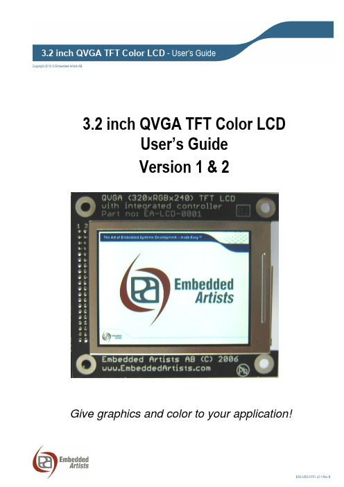
Copyright 2012 © Embedded Artists AB3.2 inch QVGA TFT Color LCDUser’s GuideVersion 1 & 2Give graphics and color to your application!Embedded Artists ABDavidshallsgatan 16SE-211 45 MalmöSweden************************Copyright 2005-2012 © Embedded Artists AB. All rights reserved.No part of this publication may be reproduced, transmitted, transcribed, stored in a retrieval system, or translated into any language or computer language, in any form or by any means, electronic, mechanical, magnetic, optical, chemical, manual or otherwise, without the prior written permission of Embedded Artists AB.DisclaimerEmbedded Artists AB makes no representation or warranties with respect to the contents hereof and specifically disclaim any implied warranties or merchantability or fitness for any particular purpose. Information in this publication is subject to change without notice and does not represent a commitment on the part of Embedded Artists AB.FeedbackWe appreciate any feedback you may have for improvements on this document. Please send your comments to ***************************.TrademarksAll brand and product names mentioned herein are trademarks, services marks, registered trademarks, or registered service marks of their respective owners and should be treated as such.Table of Contents1Document Revision History4 2Introduction5 2.1Features5 2.2Version 1 vs. Version 25 2.3ESD Precaution6 2.4General Handling Care6 2.5CE Assessment6 2.6Other Products from Embedded Artists6 2.6.1Design and Production Services6 2.6.2OEM / Education / QuickStart Boards and Kits7 3Design Description8 3.1Backlight Control8 3.2On-board LCD Controller, display version 28 3.3On-board touch screen Controller, display version 29 3.4On-board LCD Controller, display version 19 3.5Interface (pin description)10 3.6Optimum Viewing Angle13 3.7Connecting version 2 to OEM Base Board < v1.514 4Board Mechanical Dimensions161 Document Revision History2 IntroductionThank you for buying Embedded Artists’ 3.2 inch QVGA TFT Color LCD Board based on a LCD from Truly. Sample applications for our NXP LPC2xxx based boards are also provided and can be downloaded from the support page. The 3.2 inch QVGA TFT Color LCD Board will be called the QVGA LCD Board for short in the rest of this document.2.1 FeaturesThe QVGA LCD Board has the following features:∙Optional touch screen interface (available for version 2)∙8-bit or 16-bit parallel interface. Only occupies 2 addresses (i.e., one address pin) or serial 8-bit (SPI-like) interface (max 10 MHz clock)∙Diagonal size: 3.2 inch∙Display technology: TFT∙Display mode: Transmissive∙No of pixels: 240xRGBx320 (QVGA size)∙Supply voltage: 3.0-3.3V∙White LED backlight, with PWM control∙View area: 48.6 x 64.8 mm∙Dot size: 0.2025 x 0.2025 mm∙Operating temperature: -20 to + 70 degrees Celsius∙No of colors: 262K (if 18-bit mode), 65k (if 16-bit mode)∙2x20 pos connector (100 mil spacing) is required to interface the module, plus optional 1x6 pos connector∙Small form factor: 93 x 83 mm2.2 Version 1 vs. Version 2There exist two versions of the display. Version 1 uses a display from one display manufacturer and version 2 uses a display from another manufacturer.The similarities between the versions are:∙Same physical size of display module.∙Same optical features and capabilities.∙Same main 2x20 pos interface connector (100 mil spacing).The differences are:∙Different internal display controllers are used. The programming interface is not identical but very similar. A reference software driver exists that supports both versions simultaneous.∙Version 2 of the display module has a touch screen option.∙ A 6 pos extra interface connector has been added beside the main 2x20 pos interface connector. This extra connector carries signals for touch screen interface and some extrasignals for direct RGB-control of display (useful when interfacing the LPC2478 MCU from2.3 ESD PrecautionPlease note that the QVGA LCD Board comes without any case/box and allcomponents are exposed for finger touches – and therefore extra attention mustbe paid to ESD (electrostatic discharge) precaution.Make it a habit always to first touch a ground pin/hole for a few secondswith both hands before touching any other parts of the boards. That way,you will have the same potential as the board and therefore minimize the risk forESD.Note that Embedded Artists does not replace boards that have been damaged by ESD.2.4 General Handling CareHandle the QVGA LCD Board with care. The boards are not mounted in a protective case/box and are not designed for rough physical handling. Connectors can ware out after excessive use. The QVGA LCD Board is designed for prototyping use, and not for integration into an end-product.Do not exercise excessive pressure on the LCD glass area. That will damage the display. Also, do not apply pressure on the flex cables connecting the LCD/touch screen. These are relatively sensitive and can be damaged if too much pressure is applied to them.Note that Embedded Artists does not replace boards where the LCD has been improperly handled.2.5 CE AssessmentThe QVGA LCD Board is CE marked. See separate CE Declaration of Conformity document.The QVGA LCD Board is a class A product. In a domestic environment this product may cause radio interference in which case the user may be required to take adequate measures.EMC emission test has been performed on the QVGA LCD Board when connected to Embedded Artists base boards. Connecting the board to other devices may alter EM C emission. It is the user’s responsibility to make sure EMC emission limits are not exceeded when connecting the board to other devices.Due to the nature of the QVGA LCD Board – an evaluation board not for integration into an end-product – fast transient immunity tests and conducted radio-frequency immunity tests have not been executed. Externally connected cables are assumed to be less than 3 meters. The general expansion connectors where internal signals are made available do not have any other ESD protection than from the chip themselves. Observe ESD precaution.Note that the QVGA LCD Board can also be considered to be a component if integrated into another product. The CE mark on the QVGA LCD Board cannot be extended to include the new (user created) product. It is the user’s responsibility to make sure EMC emission limits are not exceeded and CE mark the final product.2.6 Other Products from Embedded ArtistsEmbedded Artists have a broad range of LPC1000/2000/3000/4000 based boards that are very low cost and developed for prototyping / development as well as for OEM applications. Modifications for OEM applications can be done easily, even for modest production volumes. Contact Embedded Artists for further information about design and production services.2.6.1 Design and Production ServicesEmbedded Artists provide design services for custom designs, either completely new or modification to existing boards. Specific peripherals and I/O can be added easily to different designs, for example,broad, and long, experience in designing industrial electronics in general and with NXP’sLPC1000/2000/3000/4000 microcontroller families in specific. Our competence also includes wireless and wired communication for embedded systems. For example IEEE802.11b/g (WLAN), Bluetooth™, ZigBee™, ISM RF, Ethernet, CAN, RS485, and Fieldbuses.2.6.2 OEM / Education / QuickStart Boards and KitsVisit Embedded Artists’ home page, , for information about other OEM / Education / QuickStart boards / kits or contact your local distributor.3 Design DescriptionThis chapter describes the hardware design of the QVGA LCD Board.3.1 Backlight ControlWhite LEDs are used as backlight on the display. The LED current is set to 15 mA. A step-up DC/DC converted is used to generate a constant LED current. The switching frequency is fixed to 1.2 MHz. The intensity of the backlight (i.e., the white LEDs) is varied by varying the LED current. There are two ways to very the LED current between 0-15 mA. A digital PWM signal is needed with the same logic levels as the power supply (typically 3.3V).∙Modulate the shutdown pin of the DC/DC converter (signal LED_SHDN). A low input signal turn off the DC/DC converted and a high level activate it. A high duty cycle on the PWM signal equals high intensity.∙Modulate the current set pin of the DC/DC converter (signal LED_PWM). A low input signal increase the LED current and a high level reduce it. A high duty cycle on the PWM signalequals low intensity.The frequency of the modulation (PWM) signal should ideally be in the 5-10 kHz region.3.2 On-board LCD Controller, display version 2The display has an embedded controller, SSD1289 from Solomon Systech. This controller chip has 1.3 Mbit embedded display RAM, which is enough for storing a complete 320xRGBx240 picture with 18 bit color depth.There are a couple of interface alternatives to this controller. Either 18-bit, 16-bit, 9-bit or 8-bit parallel interface or a serial interface. There are 4 pins that are used to configure the interface. The table below lists the different options. L is statically tied to low logic level and H is statically tied to high logic level.If the parallel interface is selected, there are two different interface types; either 6800 or 8080 style. See datasheet for details about timing and how the different control signals are used.If a serial interface is used, see the datasheet for details about timing and how the different control signals are used. Note that maximum clock frequency is 13 MHz.3.3 On-board touch screen Controller, display version 2The touch screen controller used is TSC2046 from Texas Instruments. This chip has a SPI interface and shares the SI, SO, SCK pins in the main interface connector, with the LCD controller. Pin 45 must however be low (TSC2046 chip CS#) in order to communicate with the touch screen controller. See TSC2046 datasheet for details about the serial interface.3.4 On-board LCD Controller, display version 1The display has an embedded controller, IS2102B from ISRON. This controller chip has 1.3 Mbit embedded display RAM, which is enough for storing a complete 320xRGBx240 picture with 18 bit color depth.There are a couple of interface alternatives to this controller. Either 16-bit or 8-bit parallel interface or a serial interface. There are 6 pins that are used to configure the interface. The table below lists the different options. L is statically tied to low logic level and H is statically tied to high logic level.If the parallel interface is selected, there are two different interface types. The configuration pin C86 is used to select between the i86 interface and the M68 interface. See datasheet for details about timing and how the different control signals are used.If a serial interface is used, see the datasheet for details about timing and how the different control signals are used. Note that maximum clock frequency is 10 MHz.3.5 Interface (pin description)The table below describes the 40 pin interface to the QVGA LCD Module. A 2x20 pos (100 mil spacing) header connector facing down is used. See datasheet for details about interface timing.On display version 2 a new extra 1x6 pos (100 mil spacing) header connector facing down exists. See datasheet for details about interface timing.The picture below illustrates the pin numbering of the QVGA LCD Module .Figure 1 - 3.2 inch QVGA TFT Color LCD Board Pin NumberingPin2Pin403.6 Optimum Viewing AngleOptimum viewing angles are as illustrated below.Figure 2 - 3.2 inch QVGA TFT Color LCD Board Optimum Viewing Angle3.7Connecting version 2 to OEM Base Board < v1.5Version 1.5 and above of the OEM Base Board has direct connectors for all 46 positions in theinterface connector. Version 1.4 and below do not have the 6 extra positions (pos 41-46). These have been added for version2 of the display.The touch screen controller can still be accessed with just one extra wire, from pin 45 on the display module to P0.16 on the OEM Base Board. P0.16 is used for chip select of the touch screen controller. Other pins work just as well, but P0.16 is used on v1.5 and above of the OEM Base Board.Figure 3 - 3.2 inch QVGA TFT Color LCD Board Pin 45Simply connect a wire from pin 45 on the display module to P0.16 on the OEM Base Board. Figure 4 and 5 below illustrate the wire connection. Also note that the three SPI jumpers must be inserted, see Figure 4 for details.Figure 4 – Picture of Wire to Pin 45 on Display Module Figure 5 – Wire to p0.16 on OEM Base Board Three SPI jumpers must be inserted since communication with touch screen controller is via SPI.4 Board Mechanical DimensionsFigure 6 below contains a drawing of the board that includes mechanical measures. Four 4.3 mm grounded mounting holes are used.Figure 6 - 3.2 inch QVGA TFT Color LCD Board Mechanical Dimensions70 mm 93 mm80.0 mm 6.5 mm。