Ch_11_Intel_Pkg_Spec
TPM Interface Specification (TIS)
7.1
Number of PCRs ................................................................................................................................. 19
7. PCR Requirements ......................................................................................................................................... 19
1.1
Terminology........................................................................................................................................... 7
TCG Published
Specification Version 1.2; Revision 1.00
Contents
1. TPM Requirements General Introduction ......................................................................................................... 7
Except that a license is hereby granted by TCG to copy and reproduce this specification for internal use only.
黑苹果显卡驱动详解
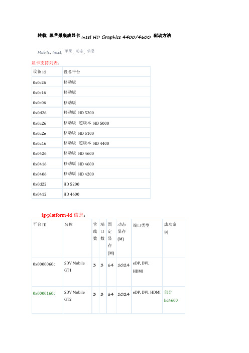
转载黑苹果集成显卡Intel HD Graphics 4400/4600 驱动方法Mobile, Intel, 苹果, 动态, 信息显卡支持列表:设备id设备平台0x0c26移动版0x0c16移动版0x0c06移动版0x0d26移动版HD 52000x0a26移动版超级本HD 50000x0a2e移动版HD 51000x0a16移动版超级本HD 44000x0426移动版HD 46000x0416移动版HD 46000x0406移动版HD 42000x0d22HD 52000x0412HD 4600ig-platform-id信息:平台ID名称管线数端口数固定显存(M)动态显存(M)端口类型成功案例0x0000060c SDV MobileGT133641024eDP, DVI,HDMI0x0000160c SDV MobileGT233641024eDP, DVI, HDMI部分hd46000x0000260c SDV MobileGT333641024eDP, DVI, HDMI i5-4570hd46000x00000604Mobile GT133641024eDP, DVI, HDMI0x00001604Mobile GT233641024eDP, DVI, HDMI0x00002604Mobile GT333641024eDP, DVI, HDMI0x0000260d CRWMobile GT333641024eDP, DVI, HDMI0x0000160a ULT Mobile GT233641024eDP, DVI, HDMI i5-4500uhd44000x0000260a ULTMobile GT333641024eDP, DVI, HDMI0x02001604Mobile GT211641024eDP0x0500260a ULT MobileGT333321024eDP, DP,DP0x0600260a ULT MobileGT333321024eDP, DP, DP i5-4200uhd44000x0800260a ULT MobileGT333641024eDP, DP,Thunderbolt0x08002e0a ULT reservedGT333640x0700260d CRW MobileGT334641024eDP, DP, DP,HDMI0x0300220d CRW DesktopGT233641024DP, DP, DP0x04001204Desktop GT20064256无个人建议,先尝试使用参数驱动。
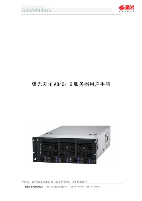
曙光天阔A840r-G用户手册V1.1
硬件及数据损坏负责; 8、 当服务器出现故障时,如果您不能确定故障的原因,请及时与曙光技术支持部门联系以
获得帮助; 9、 如主板 CMOS 电池失效,请使用与本机配备的电池相同型号的电池进行更换,替换下的
的稳定运行,并将可以延长服务器的使用寿命; 2、 请使用带接地保护的三芯电源线与插座,并使用220V 交流电,不正确的电源设置可能
会导致漏电、烧毁、爆炸甚至人身伤害; 3、 请不要在服务器正在运行时插拔背板连线或是移动服务器,否则将可能造成服务器当机
或是部件损坏; 4、 请尽量避免频繁重启或开关机,以延长服务器的使用寿命; 5、 请用户及时备份重要数据,曙光信息产业有限公司不为任何情况导致的数据丢失负责; 6、 请使用正版操作系统及软件,并进行正确配置。曙光信息产业有限公司对由于操作系统
声明及注意事项
感谢您选用曙光服务器!
曙光服务器将给您带来强大的应用支持和全新的性能体验。为了您能够更安全、方便的 使用曙光服务器,在使用之前,请详细阅读本节所提示的信息。
曙光服务器在设计和制造过程中均遵循了严格的标准,以保证您所使用的服务器拥有卓 越的品质和完美的“SUMA”特性。但是服务器属于精密电子设备,在使用过程中仍然可能因 为各种原因而导致异常,所以请务必明确以下事项: 1、 请将服务器放置在阴凉、干燥、通风、洁净、无强磁场的环境中使用,这有助于服务器
电池请妥善回收处理。 曙光信息产业有限公司保留对以上条款的解释权。
再次感谢您选用曙光服务器!
-3-
曙光天阔 A840r-G 服务器用户手册 V1.1
目录
第一章 系统简介 ........................
提升基于英特尔架构的 Android 模拟器的速度
提升基于英特尔®架构的 Android* 模拟器的速度Costas Styliano...于星期五, 04/10/2013 - 00:21 提交摘要:如果您是一名Android* 开发人员,而且对Android 模拟器的性能不满意,请阅读本文。
我们经常听到许多Android 开发人员抱怨模拟器速度缓慢而且难以操作,但是事实并不应该如此!如果您使用的是采用英特尔®处理器且支持英特尔®虚拟化技术并运行Microsoft Windows* 或Apple Mac OS* 的新电脑,那么您可以使用英特尔®硬件加速执行管理器(英特尔® HAXM)或KVM for Linux* 来轻松地大幅提升Android 模拟器的性能,进而加快Android 应用的测试和调试速度。
本文详细介绍了加速模拟器所需的步骤以及如何对其进行操作。
然后,我们将介绍如何使用NDK 编译x86 原生代码以及如何将包含x86 原生库的APK 提交至Google Play 商店。
英特尔HAXM 还可用于加速Tizen* 模拟器,但这不在本文的讨论范围之内。
如欲获取更多信息,请访问,了解SDK 部分的内容。
目录1. 简介2. 安装2.1. 前提条件2.2. 在Windows 上安装2.3. 在Linux 上安装2.3.1. KVM 安装2.4. 创建AVD(Android* 虚拟设备)3. 公认的最佳方法3.1. 在Eclipse 中使用模拟器测试应用3.2. 提交多种面向不同ABI 的APK 与提交fat 二进制文件至Google Play3.3. 编译面向x86 的NDK3.3.1. 将NDK 路径添加至环境变量3.3.2. 使用NDK 编译3.3.3. 使用NDK 编译的其他方法1. 简介本文将为您安装英特尔®硬件加速执行管理器(英特尔® HAXM)提供指导。
英特尔® HAXM 是一款硬件辅助虚拟化引擎(管理程序),它可通过英特尔®虚拟化技术(英特尔® VT)在Windows* 上加快Android* 开发速度。
LTP使用说明
LTP工具说明1LTP测试套件 (3)1.1简介 (3)1.2源目录结构 (3)2LTP安装 (4)2.1下载 (4)2.2编译 (4)2.3安装说明 (5)3LTP测试套件结构说明 (6)3.1概述 (6)3.2目录介绍 (6)3.3LTP执行原理 (6)4LTP测试套件测试内容 (7)4.1LTP测试套件测试内容 (7)4.1.1commands (7)4.1.2kernel (7)4.1.3kdump (8)4.1.4network (8)4.1.5realtime (8)4.1.6open_posix_testsuite (8)4.1.7misc (8)4.2测试方法说明 (8)4.2.1commands模块内容描述及实现方法 (8)4.2.2kernel (10)4.2.3network (15)4.2.4open_posix_testsuite (17)4.2.5realtime (18)5LTP测试套件配置详细 (19)5.1networktests.sh脚本配置 (19)5.2networkstress.sh配置 (23)5.3open_posix_testsuite测试套件 (28)5.4realtime配置 (29)5.5mm脚本的配置 (30)5.6io脚本配置 (30)5.7filecaps的配置 (30)5.8tpm_tools的配置 (31)5.9tcore的配置 (31)5.10io_floppy的配置 (31)5.11io_cd 的配置 (32)5.12cpuhotplug的配置 (32)5.13adp.sh的配置 (33)5.14autofs1.sh和autofs4.sh的配置 (34)5.15exportfs.sh的配置 (34)5.16isofs.sh的配置 (34)5.17ltpdmmapper.sh的配置 (35)5.18ltpfslvm.sh的配置及要求 (36)5.19ltpfsnolvn.sh的配置及要求 (36)5.20ltp-scsi_debug.sh的配置及要求 (37)5.21sysfs.sh的配置及要求 (37)5.22rpctirpc的配置及要求 (37)5.23test_selinux.sh的配置及要求 (39)5.24smack的配置和要求 (40)5.25perfcounters的配置及要求 (41)5.26can的配置及要求 (41)5.27test_robind.sh的配置 (42)6LTP测试套件使用说明 (43)6.1概述 (43)6.2测试方法 (44)6.2.1初始测试 (44)6.2.2压力测试 (47)1LTP测试套件1.1简介LTP(Linux Test Project)是SGI、IBM、OSDL和Bull合作的项目,目的是为开源社区提供一个测试套件,用来验证Linux系统可靠性、健壮性和稳定性。
Intel 桌面母板 D845GVSR 产品指南

Intel Corporation 5200 N.E. Elam Young Parkway Hillsboro, OR 97124 1-800-628-8686
本设备已经过测试,符合 FCC 条例第 15 部分对 B 类数字设备的限制要求。这些限制旨在提供合理的保护措施,以防止在居 住区安装本设备时可能产生的有害干扰。本设备将产生、使用并可能辐射无线电射频能。如果未按说明安装和使用本设备, 可能会对无线电通信造成有害干扰。然而,在特定条件下的正确安装并不保证不会产生此类干扰。如果本设备确实对无线电 通信或电视接收产生了有害干扰(通过关闭和打开本设备可以判定有无干扰产生),用户可采取以下一种或几种措施以消除 干扰: • 改变接收天线的方向或位置。
本数字设备未超过对无线电噪声辐射的 B 类限制,此限制是加拿大通信部颁布的《无线电干扰规则》(Radio Interference Regulations) 中对数字设备的限制性规定。
Le présent appareil numerique német pas de bruits radioélectriques dépassant les limites applicables aux appareils numériques de la classe B prescrites dans le Réglement sur le broullage radioélectrique édicté par le ministére des Communications du Canada.
iv
目录
1 桌面母板功能
桌面母板组件...................................................................................................................... 11 处理器 ................................................................................................................................ 13 主内存 ................................................................................................................................ 14 Intel® 845GV 芯片组........................................................................................................... 15 音频子系统 ......................................................................................................................... 15 LAN 子系统(可选) .......................................................................................................... 16
Fuji Xerox维修手册 Ver.2

6.2.3 Jam Counter ..........................................................
8
6.2.4 Fail Counter .........................................................
8
6.2.5 Shutdown History .....................................................
9
6.2.6 NVM Read / Write ..................................................... 10
6.2.15 Tray 5 (Bypass) Guide Adjustment .................................... 39
6.2.16 IIT Calibration ..................................................... 40
6.3.1 IOT xx ESS IF ........................................................ 43 Chain 740-xxx Recycle ....................................................... 43 Chain 740-xxx Billing ....................................................... 44 Chain 740-xxx 742-xxx 751-xxx 760-xxx PH .................................... 45 Chain 740-xxx 749-xxx 751-xxx XERO .......................................... 48 Chain 741-xxx Drive ......................................................... 49 Chain 741-xxx NOHAD ......................................................... 50 Chain 742-xxx TRAY .......................................................... 51 Chain 742-xxx 764-xxx EXIT .................................................. 54 Chain 744-xxx FUSER ......................................................... 55 Chain 749-xxx ROS ........................................................... 56 Chain 751-xxx CRU ........................................................... 57 Chain 751-xxx 752-xxx 753-xxx Procon ........................................ 59 Chain 763-xxx Finisher-C .................................................... 61 Chain 764-xxx Finisher-B .................................................... 74
FCC声明说明书

Federal Communications Commission (FCC) Statement (011898)This equipment has been tested and found to comply with the limits for a Class B digital device, pursuant to Part 15 of FCC Rules. These limits are designed to provide reasonable protection against harmful interference in a residential installation. This equipment generates, uses and can radiate radio frequency energy and, if not installed and used in accordance with instructions contained in this manual, may cause harmful interference to radio and television communications. However, there is no guarantee that interference will not occur in a particular installation.If this equipment does cause harmful interference to radio or television reception, which can be determined by turning the equipment off and on, the user is encouraged to try to correct the interference by one or more of the following measures:-REORIENT OR RELOCATE THE RECEIVING ANTENNA-INCREASE THE SEPARATION BETWEEN THE EQUIPMENT AND THE RECEIVER -CONNECT THE EQUIPMENT INTO AN OUTLET ON A CIRCUIT DIFFERENT FROM THAT OF THE RECEIVER-CONSULT THE DEALER OR AN EXPERIENCED AUDIO/TELEVISION TECHNICIANNOTE:Connecting this device to peripheral devices that do not comply with Class B requirements, or using an unshielded peripheral data cable, could also result in harmful interference to radio or television reception.The user is cautioned that any changes or modifications not expressly approved by the party responsible for compliance could void the user’s authority to operate this equipment.To ensure that the use of this product does not contribute to interference, it isnecessary to use shielded I/O cables.CopyrightThis manual is copyrighted with all rights reserved. No portion of this manual may be copied or reproduced by any means.While every precaution has been taken in the preparation of this manual, no responsibility for errors or omissions is assumed. Neither is any liability assumed for damages resulting from the use of the information contained herein.TrademarksAll brand names, logos and registered trademarks mentioned are property of their respective owners.Table of ContentsHARDWARE CONFIGURATION (3)Key Features (3)Motherboard Layout (5)Jumper Settings (6)CPU Speed Selection (6)SW1, SW2 - CPU Frequency Ratio (6)SW3 - VID[0:4] Code to Voltage Definition (7)J7 - CMOS Clear (8)J2 - On Board AC97 Codec Sound (8)Pin Assignment (9)HARDWARE SETUP (10)T o Install DIMMs (10)Installing a New Processor (11)To Install a Processor to ZIF Socket (11)Connect the processor Fan Connector (11)BIOS SETUP (12)Starting Setup (12)Main Menu (13)Standard CMOS Features (14)Advanced BIOS Features (16)Advanced Chipset Features (16)Integrated Peripherals (16)Power Management Setup (16)PnP/PCI Configurations (16)PC Health Status (16)Frequency/Voltage Control (16)Set Supervisor/User Password (16)Flash Update Procedure (18)APPENDIX (19)Select the Heatsink (19)Select the Power Supply (20)HARDWARE CONFIGURATIONKey Features:Chipset•VIA® KT133/KT133A Chipset.Processor•Full support for the AMD Duron TM and Athlon TM processors using Socket A.•Supports 100MHz & 133MHz (optional) bus speed including all processors using Socket A.VRM 9.0 (Voltage Regulator Modules) on Board•Flexible motherboard design with on board VRM 9.0.System Memory• A total of three 168-pin DIMM sockets (3.3V Synchronous DRAM).•Supports Synchronous DRAM PC100/PC133.•Memory size up to 1.5G bytes.•Supports SDRAM memory types.•Supports single-density DIMMs of 1MB, 2MB, 4MB, 8MB and 16MB depth (x64).•Supports double-density DIMMs of 2MB, 4MB, 8MB, 16MB and 32MB depth (x64).•Supports single & double sided DIMMs.•Banks of different DRAM types depths can be mixed.System BIOS•2MB flash BIOS supporting PnP, APM, ATAPI and Windows® 95.•Auto detects and supports LBA hard disks with capacities up to 8.4GB.•Full support of ACPI & DMI.•Easy to upgrade BIOS by end-user.Dual BIOS•As our dual BIOS use the awdflash ver.7.83 to flash the dual BIOS, so our dual BIOS support the flash type of the awdflash ver.7.83, such as Syncmos,ATMEL etc..•The normal boot sequence is from main BIOS. If one BIOS is fail to boot, you can press the ‘Reset’ button to boot from the other BIOS (Note: no every time issuccess, you can try it several times or touch button time is enough long, forexample 2~3 second).•If the BIOS error that contained in compressed part of BIOS bin file, our dual BIOS can know to automatic flash, but the boot block error can not know to flash, that is: If the BIOS bin file is damage, it will auto flash BIOS, and if the bin file is OKeven different with the board bin file, computer will boot normal without enter the flash screen). If the user want to flash the BIOS unconditionally, you can press the ‘Alt + F2’ key to flash another BIOS.On-board I/O•On board two PCI fast IDE ports supporting up to 4 ATA and Ultra DMA33/66/ 100 (optional) IDE devices.•Supports bus master IDE, PIO mode 4 (up to 16.6M bytes/sec) and Ultra DMA33/66/100 (optional) (up to 33/66/100M (optional) bytes/sec) transfer.•One ECP/EPP parallel port.•Two 16550-compatible UART serial ports.•One floppy port, supports two FDDs of 360KB, 720KB, 1.2MB, 1.44MB and 2.88MB capacity.•Four USB ports.•PS/2 mouse port.•PS/2 keyboard port.•Infrared (IrDA) is supported.•One Line/Speaker out, one Mic in, one Line in and MIDI/Game port (optional).Plug-and-Play•Supports plug-and-play specification 1.1.•Plug-and-play for DOS, Windows® 3.X, Windows® 95 as well as Windows® 98.•Fully steerable PCI interrupts.On-board AC97 Sound•Integrated AC97 controller with standard AC97 codec.•Direct Sound and Sound Blaster compatible.•Full-Duplex 16-bit record and playback.•PnP and APM 1.2 support.On-board Creative Sound (optional)•Creative ES1373 Audio controller.•128 voice wave table synthesizer.•DOS game compatibility.•PCI bus master for fast DMA.•Fully compliant with PC97 power management specification.(Note: If Creative PCI Sound is on board, only Primary AMR Card can be used. If Creative PCI Sound is enabled, Bus Master Device on one PCI cannot be used.)Power Management•Supports SMM, APM and ACPI.•Break switch for instant suspend/resume on system operations.•Energy star “Green PC” compliant .•WOL (Wake-On-Lan) Header support.•External Modem Ring-in Wake-up support.•Support auto setting or manual setting for CPU voltage.•Supports suspend-to-RAM (STR) (optional).Expansion Slots• 5 PCI bus master slots (Rev. 2.1 compliant).• 1 Audio Modem Riser (AMR) (optional).• 1 ISA slot (1 ISA slot share with 1 PCI slot).• 1 universal AGP slot (AGP 2.0 compliant - 4X mode support).CAUTIONStatic electricity can harm delicate components of the motherboard. To prevent damage caused by static electricity, discharge the static electricity from yourbody before you touch any of the computers electronic components.Motherboard LayoutThe following diagrams show the relative positions of the jumpers, connectors, major components and memory banks on the motherboard.# The AMR slot is optional.NOTE1)Be sure to check the cable orientation in order to match the colored strip tothe pin 1 end of the connector.2)When you start up the system, please wait for 5 seconds after you poweron AC.Jumper SettingsThis chapter explains how to configure the motherboard’s hardware. Before using your computer, make sure all jumpers and DRAM modules are set correctly. Refer to this chapter whenever in doubt.CPU Speed SelectionIn this motherboard, you can set the CPU speed by manual or auto way, but over clock isn’t recommended.SW1, SW2 - CPU Frequency RatioSW2[1:5]SW1[1:4] SW2[1:5] CPU FREQ1 2 3 4 5SW3 - VID[0:4] Code to Voltage DefinitionSW1(6) Off, Auto Setting SW1(6) On, Manual Setting。
- 1、下载文档前请自行甄别文档内容的完整性,平台不提供额外的编辑、内容补充、找答案等附加服务。
- 2、"仅部分预览"的文档,不可在线预览部分如存在完整性等问题,可反馈申请退款(可完整预览的文档不适用该条件!)。
- 3、如文档侵犯您的权益,请联系客服反馈,我们会尽快为您处理(人工客服工作时间:9:00-18:30)。
International Packaging Specifications 11 11.1Electronic Industries Association of Japan (EIAJ)
EIAJ publishes the following rules and standards as they apply to the preparation of outline
drawings of integrated circuits.
Number Nomenclature
ED -7300Recommended practice on standard for the preparation of outline drawings of
semiconductor packages
ED -7301Manual or the standard of integrated circuits package
ED -7302Manual for integrated circuits package design guideline
ED -7303Name and code for integrated circuits package
ED -7304Measuring method for package dimensions of ball grid array (BGA)
ED -7304-1Measuring method for package dimensions of Small Outline Package (SOP)
ED -7304-2Measuring method for package dimensions of Small Outline J-leaded package (SOJ)
ED -7305Unit design guide for the preparation of package outline drawing of integrated circuits
(gullwing-lead)
ED -7311Standards of integrated circuits package
ED -7311-1Standard of integrated circuits package [TSOP(1)]
ED -7311-2Standard of integrated circuits package [TSOP(2)]
ED -7311-3Standard of integrated circuits package [Tape Ball Grid Array 1.0mm pitch (T-BGA)]
ED -7311-4Standard of integrated circuits package [Tape Ball Grid Array 1.27mm pitch (T-BGA)]
ED -7311-5Standard of integrated circuits package [32/48 pins Fine-pitch Ball Grid Array (FBGA)]
ED -7311-6Standard of integrated circuits package [60/90 pins Fine-pitch Ball Grid Array (FBGA)]
ED -7311-7Standard of integrated circuits package [Plastic Fine pitch Ball Grid Array (P-FBGA)]
ED -7311-8Standard of integrated circuits package [Plastic Fine pitch Ball Grid Array 0.8mm pitch (P-
FBGA)]
ED -7311-9A Standard of integrated circuits package [P-BGA (Cavity up type)]
ED -7311-10A Standard of integrated circuits package [P-BGA (Cavity down type)]
ED -7311-11A Standard of integrated circuits package (119/153 pins P-BGA)
ED -7311-12Standard of integrated circuits package (52 pins 64 pins 80 pins and 100 pins low-profile
quad flat package with exposed heatsink)
ED -7400Standards for the dimensions of semiconductor devices (integrated circuits)
ED -7400-1Standards for the dimensions of semiconductor devices (integrated circuits)
ED -7400-2Standards for the dimensions of semiconductor devices (integrated circuits)
ED -7401-4Method of measuring semiconductor device package dimensions (integrated circuits)
ED -7405General rules for the preparation of outline drawings of integrated circuits zigzag in-line
packages (ZIP)
ED -7405-1General rules for the preparation of outline drawings of integrated circuits shrink zigzag
in-line packages (SZIP)
International Packaging Specifications
International Packaging Specifications。