JE892HSGL2中文资料
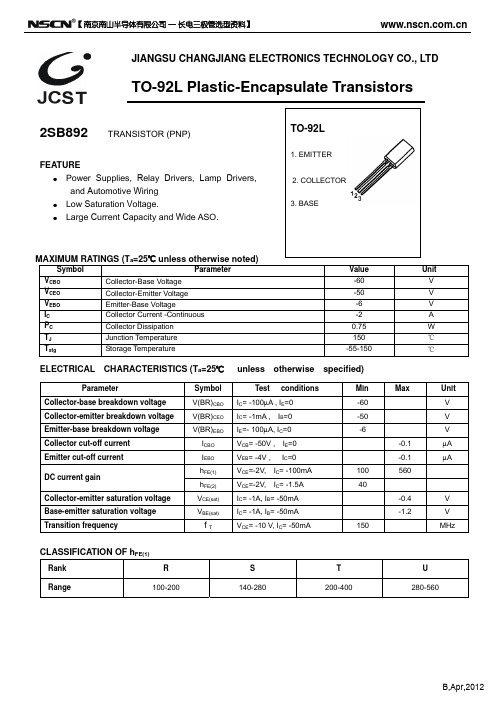
2SB892三极管(TO-92L)
【 南京南山半导体有限公司 — 长电三极管选型资料】
Sponge strip
Sponge strip
2000 pcs
The top gasket
Label on the Inner Box
Inner Box: 333 mm×203mm×42mm
Stamp “EMPTY” on the empty box
FEATURE z Power Supplies, Relay Drivers, Lamp Drivers, and Automotive Wiring z Low Saturation Voltage. z Large Current Capacity and Wide ASO.
TO-92L
1. EMITTER 2. COLLECTOR 3. BASE
2.440
2.640
13.800
14.200
1.600
0.000
0.300
Dimensions In Inches
Min.
Max.
0.146
0.161
0.050
0.062
0.014
0.022
0.024
0.031
0.014
0.018
0.185
0.201
0.157
0.307
0.323
0.050 TYP.
-150
COMMON EMITTER Ta=25℃-Fra bibliotek00-50
-0.50mA -0.45mA -0.40mA -0.35mA -0.30mA -0.25mA -0.20mA
-0.15mA -0.10mA
-0 -0.0
SY89297UMH;SY89297UMG;SY89297UMG TR;SY89297UMH TR;中文规格书,Datasheet资料

SY89297U2.5/3.3V, 3.2Gbps Precision CML Dual-Channel Programmable DelayPrecision Edge is a registered trademark of Micrel, Inc.Micrel Inc. • 2180 Fortune Drive • San Jose, CA 95131 • USA • tel +1 (408) 944-0800 • fax + 1 (408) 474-1000 •General DescriptionThe SY89297U is a DC-3.2Gbps programmable, two-channel delay line. Each channel has a delay range from 2ns to 7ns (5ns delta delay) in programmable increments as small as 5ps. The delay step is extremely linear and monotonic over the entire programming range, with 15ps INL over temperature and voltage.The delay varies in discrete steps based on a serial control word provided by the 3-pin serial control (SDATA, SCLK, and SLOAD). The control word for each channel is 10-bits. Both channels are programmed through a common serial interface. For increased delay, multiple SY89297U delay lines can be cascaded together.The SY89297U provides two independent 3.2Gbps delay lines in an ultra-small 4mm x 4mm, 24-pin QFN package. For other delay line solutions, consider the SY89295U and SY89296U single-channel delay lines. Evaluation boards are available for all these parts.Datasheets and support documentation can be found on Micrel’s web site at: .Precision Edge ®Features• Dual-channel, programmable delay line• Serial programming interface (SDATA, SCLK, SLOAD) • Guaranteed AC performance over temperature and voltage:– > 3.2Gbps/1.6GHz f MAX • Programming Accuracy: – Linearity: −15ps to +15ps INL – Monotonic: −5ps to +25ps– Resolution: 5ps programming increments • Low-jitter design: 1ps RMS typical random jitter • Programmable delay range: 5ns delay range • Cascade capability for increased delay • Flexible voltage operation:– V CC = 2.5V ± 5% or 3.3V ± 10% • Industrial temperature range: −40°C to +85°C • Available in 24-pin (4mm x 4mm) QFNApplications• Clock de-skewing • Timing adjustments • Aperture centering • System calibrationMarkets• Automated test equipment• Digital radio and video broadcasting • Closed caption encoders/decoders • Test and measurementOrdering Information(1)Part Number Package Type Operating Range Package Marking Lead FinishSY89297UMG QFN-24 Industrial 297U with Pb-Free Bar Line Indicator Pb-Free NiPdAuSY89297UMGTR(2)QFN-24 Industrial 297U with Pb-Free Bar-Line Indicator Pb-Free NiPdAuNotes:1. Contact factory for die availability. Dice are guaranteed at T= 25°C, DC electricals only.A2. Tape and Reel.Pin Configuration24-Pin QFNTruth TablesInputs Outputs INA, INB /INA, /INB QA, QB /QA, /QB0 1 0 11 0 1 0Table 1. Inputs/Outputs/ENA, /ENB Q, /Q (A, B)1 Q = Low, /Q = HIGH0 IN, /IN Delayed (normal operation)Table 2. Input Enable (Latches Outputs)Functional Block DiagramPin DescriptionPin NumberPin Name Pin Function1 2INA /INAChannel A Differential Input: INA and /INA pins receive the Channel A data. QA and /QA are the delayed product of INA and /INA. Each input is internally terminated to VTA through a 50Ω resistor (100Ω across INA and /INA).3 VTA Input A Termination Center-Tap: Each side of the differential input pair terminates to this pin.This pin provides a center-tap to a termination network for maximum interface flexibility. See“Input Interface Applications” section. 4 VTBInput B Termination Center-Tap: Each side of the differential input pair terminates to this pin. This pin provides a center-tap to a termination network for maximum interface flexibility. See “Input Interface Applications” section. 5 6INB /INBChannel B Differential Input: INB and /INB pins receive the Channel B data. QB and /QB are the delayed product of INB and /INB. Each input is internally terminated to VTB through a 50Ω resistor (100Ω across INB and /INB).7 VREF-ACReference Voltage Output: For AC-coupled input signals, this pin can bias the inputs IN and /IN. Connect VREF-AC directly to the VT input pin for each channel. De-couple to V CC using a0.01µF capacitor. Maximum sink/source current is ±0.5mA. For DC-coupled input applications, leave VREF-AC pin floating. 8, 11, 20GND, Exposed PadNegative Supply: Exposed pad must be connected to a ground plane that is the same potential as the ground pins.9 /ENACMOS/TTL-Compatible Enable Input: When the /ENA pin is pulled HIGH, QA is held LOW and /QA goes HIGH after the programmed delay propagates through the part. /ENA contains a 67k Ω pull-down resistor and defaults LOW when left floating. Logic threshold level is V CC /2 10 /ENBCMOS/TTL-Compatible Enable Input: When the /ENB pin is pulled HIGH, QB is held LOW and /QB goes HIGH after the programmed delay propagates through the part. /ENB contains a 67k Ω pull-down resistor and defaults LOW when left floating. Logic threshold level is Vcc/2 12, 15, 16, 19VCC Power Supply: Bypass each supply pin with 0.1µF//0.01µF low-ESR capacitors. See DC Electrical Characteristics table for more details. 2.5V ±5% or 3.3V ±10%.13 14 /QB QB CML Differential Output: QB and /QB are the delayed product of INB, /INB. CML outputs are terminated at the destination with 100Ω across the pair. See “CML Output Termination” section.17 18/QA QACML Differential Output: QA and /QA are the delayed product of INA, /INA. CML outputs are terminated at the destination with 100Ω across the pair. See “CML Output Termination” section.23 22SCLK SDATACMOS/TTL-compatible 3-pin serial programming control inputs: The 3-pin serial control sets each channel’s IN to Q delay. DA(0:9) control channel A delay. DB(0:9) control channel B. To program the two channels, insert a 20-bit word (DA0:DA9 and DB0:DB9) into SDATA and clock in the control bits with SCLK. Maximum input frequency to SCLK is 40MHz. Data is loaded into the serial registers on the L-H transition of SCLK. After all 20-bits are clocked in, SLOAD latches the new delay bits. These pins have internal pull-downs at the inputs. See “ACElectrical Characteristics” for delay values. Logic threshold level is Vcc/2. SCLK and SDATA contain a 67k Ω pull-down resistor and default LOW when left floating.24 SLOADCMOS/TTL-compatible 3-pin serial programming control input: SLOAD controls the latches that transfer scanned data to the delay line. These latches are transparent when SLOAD is high. Data transfers from the latch to the delay line on a L-H transition of SLOAD. SLOAD has to transition H-L before new data is loaded in the scan chain. When SLOAD is high, the latches are transparent and SCLK cannot switch. Otherwise, new data will immediately transfer to the scan chain. Logic threshold level is Vcc/2. SLOAD contains a 67k Ω pull-down resistor and defaults LOW when left floating. 21 SOUTCMOS/TTL-compatible output: This pin is used to support cascading multiple SY89297U delay lines. Serial data is clocked into the SDATA input and is clocked out of SOUT into the next SY89297U delay line. SOUT pin includes an internal 550Ω pull-up resistor.Absolute Maximum Ratings(1)Supply Voltage (V CC) .................................. –0.5V to +4.0V Input Voltage (V IN) .......................................... –0.5V to V CC CML Output Voltage (V OUT)… ....... V CC −1.0V to V CC +0.5V Current (V T)Source or Sink Current on VT pin ..................... ±70mA Input CurrentSource or Sink Current on (IN, /IN) .................. ±35mA Current (V REF)Source or sink current on V REF-AC(2) ................ .±0.5mA Maximum operating Junction Temperature ............ 125°C Lead Temperature (soldering, 20sec.) ..................... 260°C Storage Temperature (T s) ....................... –65°C to +150°C Operating Ratings(3)Supply Voltage (V CC)T A (−40°C to +85°C) ................ +2.375V to +2.625VT A (−40°C to +75°C) .......................... +3.0V to 3.6V Ambient Temperature (T A) .......................... −40°C to +85°C Package Thermal Resistance(4)QFN (θJA)Still-Air...............................................................43°C/W QFN (ψJB)Junction-to-Board...........................................30.5°C/WDC Electrical Characteristics(5)T A = −40°C to +85°C, Channels A and B, unless otherwise stated.Symbol Parameter Condition Min. Typ. Max. UnitsV CC Power Supply Voltage Range T A: −40°C to +85°C 2.375 2.5 2.625 V T A: −40°C to +75°C 3.0 3.3 3.6 V T A: −40°C to +85°C,Airflow = 500 LFPM3.0 3.3 3.6 VI CC PowerSupplyCurrent Maximum V CC, Both ChannelsCombined, Output Load Included195 250 mAR IN Input Resistance(IN-to-VT, /IN-to-VT)455055ΩR DIFF_IN Differential Input Resistance(IN-to-/IN)90100110ΩV IH Input HIGH Voltage (IN, /IN) 1.2 V CC V V IL Input LOW Voltage (IN, /IN) 0 V IH–0.1 V V IN Input Voltage Swing (IN, /IN) See Figure 5a 0.1 1.0 VV DIFF_IN Differential Input Voltage Swing(|IN - /IN|)See Figure 5b 0.2 VV REF-AC Output Reference Voltage V CC–1.3 V CC–1.2 V CC–1.1 VV T_IN Voltage from Input to V T 1.28 V Notes:1. Permanent device damage may occur if “Absolute Maximum Ratings” are exceeded. This is a stress rating only and functional operation is notimplied at conditions other than those detailed in the operational sections of this data sheet. Exposure to “Absolute Maximum Rating” conditions for extendedperiodsmayaffectdevicereliability.2. Due to the limited drive capability, use for input of the same package only.3. The data sheet limits are not guaranteed if the device is operated beyond the operating ratings.4. Thermal performance on QFN packages assumes exposed pad is soldered (or equivalent) to the device most negative potential (GND).5. The circuit is designed to meet the DC specifications shown in the table after thermal equilibrium has been established.CML Outputs DC Electrical Characteristics (6)V CC = +2.5V +5% or +3.3V ±10%, R L = 100Ω across the outputs; T A = −40°C to +85°C, unless otherwise stated. Symbol Parameter Condition Min. Typ. Max. Units V OH Output HIGH Voltage R L = 50Ω to V CC V CC −0.020 V CC −0.010V CC VV OUT Output Voltage SwingSee Figure 5a 325 400 mV V DIFF_OUTDifferential Output Voltage SwingSee Figure 5b650 800 mV R OUT Output Source Impedance455055ΩLVTTL/CMOS DC Electrical Characteristics (6)V CC = +2.5V +5% or 3.3V ±10%, T A = −40°C to +85°C, unless otherwise stated. Symbol Parameter Condition Min. Typ. Max. Units V IH Input HIGH Voltage 2.0 V V IL Input LOW Voltage0.8 V I IH Input HIGH Current V IH = VCC 150 µA I IL Input LOW Current V IL = 0.8V50µAV OLOutput LOW Voltage SOUT Pin; I OL =1mA 0.55 VOutput High Leakage CurrentSOUT = V CC 100 µANote:6. The circuit is designed to meet the DC specifications shown in the above table after thermal equilibrium has been established.AC Electrical Characteristics (7)T A = −40°C to +85°C, Channels A and B, unless otherwise stated. Symbol Parameter ConditionMin. Typ. Max. Units f MAXMaximum Operating FrequencyClock: V out Swing >200mV pk 1.6 GHzNRZ Data3.2Gbpst pdPropagation Delay IN to Q; D[0–9]=0 IN to Q; D[0–9]=1023/EN to Q: D[0–9]=0; V TH = V CC /2 SDATA to SOUT (D0–D9=Low), No load1000 5500 1000 20002000 7500 2500 4500pst RANGE Programmable Ranget pd (max) – t pd (min)4150 5115 pst SKEWDuty Cycle Skew t PHL – t PLH Note 84555%AC Electrical Characteristics(7)T A = −40°C to +85°C, Channels A and B, unless otherwise stated.Symbol Parameter Condition Min. Typ. Max. UnitsΔt Step DelayD0 HighD1 HighD2 HighD3 HighD4 HighD5 HighD6 HighD7 HighD8 HighD9 HighD0-D9 High510204080160320640128025605115ps Monotonic −5 25INL IntegralNon-Linearity Note 9 −15 +15 pst S Setup TimeSDATA to SCLKSCLK to SLOAD/EN to INNote 10Note 11400400300pst H Hold TimeSLOAD to SCLKIN to /ENSCLK to SDATANote 12Note 13300−100200pst PW Pulse Width SLOAD 1000 ps t R Release Time /EN to IN Note 14 800 pst JITTER Cycle-to-Cycle JitterTotal JitterRandom JitterNote 15Note 16Note 172202ps RMSps PPps RMSt r, t f Output Rise/Fall Time 20% to 80% (Q) 30 55 80 ps Duty Cycle Input Frequency = 1.6GHz 45 55 % Notes:7. High frequency AC electricals are guaranteed by design and characterization.8. Duty cycle skew guaranteed only for differential operation measured from the cross point of the input to the crosspoint of the output.9. INL (Integral Non-Linearity) is defined from its corresponding point on the ideal delay versus D[9:0] curve as the deviation from its ideal delay. Themaximum difference is the INL. Theoretical Ideal Linearity (TIL) = (measured maximum delay – measured minimum delay) ÷ 1023. INL = measured delay – (measured minimum delay + (step number x TIL)).10. SCLK has to transition L-H a setup time before the SLOAD H-L transition to ensure the valid data is properly latched. See timing diagram "Setupand Hold Time: SCLK and SLOAD.”11. This setup time is the minimum time that /EN must be asserted prior to the next transition of IN / /IN to prevent an output response greater than±75 mV to that IN or /IN transition. See timing diagram Setup, Hold and Release Time: IN and /EN."12. SCLK has to transition L-H a hold time after the SLOAD H-L transition to ensure that the valid data is properly latched before starting to load newdata. See timing diagram "Setup and Hold Time: SCLK and SLOAD.”13. This hold time is the minimum time that /EN must remain asserted after a negative going transition of IN to prevent an output response greater than+75mv to the IN transition. See timing diagram “Setup, Hold, and Release Time: IN and /EN.”14. This release time is the minimum time that /EN must be de-asserted prior to the next IN / /IN transition to affect the propagation delay of IN to Qless than 1ps. See timing diagram “Setup, Hold, and Release Time: IN and /EN.”15. Cycle-to-cycle jitter definition: The variation of periods between adjacent cycles over a random sample of adjacent cycle pairs.T jitter_cc = T n – T n+1, where T is the time between rising edges of the output signal.16. Total jitter definition: With an ideal clock input, no more than one output edge in 1012 output edges will deviate by more than the specified peak-to-peak jitter value.17. Random jitter definition: Jitter that is characterized by a Gaussian distribution, unbounded and is quantified by its standard deviation and mean.Random jitter is measured with a K28.7 comma defect pattern, measured at 1.5Gbps.Timing DiagramsFigure 1. Setup and Hold Time: SDATA and SCLKFigure 2. Setup and Hold Time: SCLK and SLOADTiming Diagrams (Continued)Figure 3. Set-Up, Hold, and Release Time: IN and /ENFigure 4. SLOAD Pulse Width (TPW)Typical Operating CharacteristicsV CC = +2.5V, GND = 0V, V IN = 100mV, R L = 100Ω across the outputs, T A = 25°C.Phase Noise ChartV CC = +2.5V, GND = 0V, V IN = 100mV, R L = 100Ω across the outputs, T A = 25°C.f C: 1GHz Delay Setting: 00001 00110 (2ns)分销商库存信息:MICRELSY89297UMH SY89297UMG SY89297UMG TR SY89297UMH TR。
HP8922培训教材资料

定了一个最基本的呼叫模式。
第二步:将一部测试OK的3310进行CALL机,在现有的维修过程中我们会比 对特误码率、相位频率误差、信号的突发状态作详细的观测。 CALL机的建链过程中CALL STATUS字段下会显示呼叫状态的变化过 程:INACTIVE--PROCEEDING--ALERTING--CONNECTED。
返回第二章首页
第三章
3.1小区控制屏幕
基 本 测 试
下面我们将会学习测试GSM手机的几个基本参数,这些参数将从小区控制屏 幕(CELL CNTL)中读到,因此首先介绍一下小区控制屏幕.我们把它看成由四 个窗口构成,用1-4加以区分.
1 2
3
4
返回目录
1 .表示小区状态区 (CELL STATUS)
接器/控制器 。如图所示:
开 关
射 頻 输 出
声音旋钮
返回目录
2.1显示屏幕
仪器的CRT屏幕用来显示不同测试状态、结果、波形及信息。是 我们观测数据的主窗口.可以用键盘区左上角中的SCREEN CONTROL区 (屏幕控制区)中的5个键进行切换,改变当前屏幕的内容.
以下分别予以介绍:
CELL CONFIG: 设置基站的仿真参数。通常在仪器校准时已设置好,平时 无须修改。 CELL CNTL:小区控制屏幕。这是在维修过程使用最多的一种状态。 MEAS SYNC:测量同步屏。 PREV:返回上一屏幕。
仪器状态键
仪器提供了SAVE / RECALL (存储和调用) 功能,我们可以将用得最多的 几种测量状态存起来,需要时可迅速调用提高工作效率,下面将着重介绍.
HGJ205-92

HGJ205-921. IntroductionThe HGJ205-92 is a cutting-edge technology developed by XYZ Corporation in the field of telecommunications. This document aims to provide a comprehensive overview of the HGJ205-92, including its features, specifications, and usage scenarios.2. FeaturesThe HGJ205-92 comes with a wide range of features that make it a versatile and powerful telecommunications solution. Some of the key features include:2.1 High-Speed Data TransferThe HGJ205-92 is designed to support high-speed data transfer, allowing users to transmit and receive data at incredibly fast speeds. This feature makes the HGJ205-92 ideal for applications that require real-time data processing and transmission.2.2 Advanced EncryptionTo ensure the security of data transmitted over the network, the HGJ205-92 employs advanced encryption algorithms. This feature makes it a reliable solution for transmitting sensitive information over insecure networks.2.3 Seamless ConnectivityThe HGJ205-92 is equipped with advanced connectivity options, including support for various network protocols and seamless integration with existing communication infrastructure. This allows for easy integration into existing telecommunication networks, minimizing downtime and ensuring uninterrupted service.3. SpecificationsThe HGJ205-92 comes with the following specifications:•Data transfer rate: Up to 10 Gbps•Encryption: Advanced AES-256 encryption•Network protocols: TCP/IP, UDP, HTTP, HTTPS•Supported interface: Ethernet•Power consumption: 5W•Operating temperature: -20°C to 70°C•Dimensions: 100mm x 80mm x 20mm4. Usage ScenariosThe HGJ205-92 can be used in various telecommunications scenarios, including but not limited to:4.1 Telecommunication NetworksThe HGJ205-92 can be used in telecommunication networks to facilitate high-speed data transfer between different network devices. Its advanced encryption ensures the security of data transmission, making it a reliable choice for critical applications.4.2 Data CentersData centers often require high-speed data transfer between servers and storage devices. The HGJ205-92 can be used to establish fast and secure connections within the data center infrastructure, ensuring efficient data processing and storage.4.3 Video StreamingThe HGJ205-92 can be used in video streaming applications to enable high-quality, low-latency video transmission over the network. With its high-speed data transfer capabilities, it can deliver smooth and uninterrupted video streaming experiences.4.4 Internet of Things (IoT)As the Internet of Things continues to grow, the need for fast and secure data transmission becomes crucial. TheHGJ205-92 can be used in IoT applications to transmit sensor data in real-time, enabling efficient monitoring and control.5. ConclusionThe HGJ205-92 is a cutting-edge telecommunications solution that offers high-speed data transfer, advanced encryption, and seamless connectivity. With its wide range of features and specifications, it can be applied in various telecommunications scenarios, from telecommunication networks to data centers and IoT applications.Overall, the HGJ205-92 is a reliable and versatile solution that offers fast and secure data transmission, making it an ideal choice for organizations seeking efficient telecommunications solutions.。
Fluke 8920A、8921A和8922A多功能电压计说明书

FLUKE 8922A8920A, 8921A & 8922AAutorangingFluke's autoranging feature allows you to carry out your testing without having to change ranges manually. A range can be placed on HOLD or manually stepped up to a higher range. On HOLD, the meter will remain in a given range regardless of changes in input levels. On STEP UP, the meter will increase ranges step-by-step until the switch is released. Peaking/Dipping MeterIn addition to an accurate digital display, all Fluke Voltmeters in the 8920-Series feature an analog meter for peak and null voltage adjustments. The meter indicates O to 100 percent full scale in each range.Linear Analog OutputModels 8920A and 8922A are equipped with a rear panel output for driving X-Y or st d p chart recorders, delivering voltages proportional to the display count. A 2-volt level equals 2000 counts, a 1-volt level equals 1000 counts, etc. This feature is not available on Model 8921A. AccuracyFluke Digital Voltmeters avoid the possibilities for error so common in analog meters. The digital displays eliminate the likelihood of misreading the meter due to viewing angle problems of parallax common with analog meters. Also, the accuracy of 8920-Series Voltmeters is specified as a percent of reading rather than as percent of full scale.Percent of reading accuracy does not degrade for measurements at the low end of a scale. Front panel switching offers a choice of readings in dB or volts.Technical SpecificationsThe a ccuracy s pecifications b elow apply from 9% to 100% of full scale and from 18°C to 28°C for 90 days. For six-month specifications multiply figures by 1.5.AC Accuracy: ± % of voltage reading or ±dB (8920A/8921 A)Range 2Hz 10 H z 20Hz 50Hz 10 kHz 700V200V1%or 0.5%or 20V 0.15dB 0.1 dB 2V Not200mV Speci-5%orlied 0.5dB 2%or 1%or 20 m V 0.25 d B 0.15dB3%or 2%or 2mV0.35dB 0.25dBAC Accuracy: ± % of voltage reading or ±dB(8922A)Range 2Hz 10 H z 20Hz 50Hz 10 k HzFILTER IN I700V200V 1%or•0.15 d B 1%or 0.5%or20V 0.15 d B 0.1 d B2V 5%or200 mV 3%or• 0.5dB0.35dB2%or•0.25dB 2%or 1%or20 mV 0.25 d B 0.15 d B5%or0.5dB5%or• 5%or 3%or 2%or I2 mv0.5 d B .. 0.5dB 0.35 d B 0.25dB• Valid when AC + DC DAMPING is selected andinput has no de components.••Below 2 mV add number of digits (N) to ±5% voltage readings, where N = 5 + mV input. Or, for dBreadings. add N to ±0.5 dB, where N = 0.5 + (mVinput)2AC+DC Accuracy: Add to AC accuracy specifications (above) ±10 digits or ±0.5 dB above 2mV, or ±100 digits or ±5.0 dB below 2 mV. Forde only, add above digits to 50 Hz to 10 kHzspecificationsFunctions: True RMS measurements only. ACor AC+ DC (8920A and 8921 A); AC or AC+ DCwith damping (8922A)Maximum Input: 700V rms or 1 O OOV peak, not toexceed a volt-hertz product of 1 x 10⁸ on anyrangeMaximum Common Mode Voltage8920A and 8922A: 400 mV rms or 600 mVpeak8921A: 500V rms or 700V peakAC Common Mode Rejection: �60 dB at 50 and60 Hz with 1000 unbalanceDC Common Mode Rejection: �100 dB, 1000unbalanceCrest Factor: 7 at full scale, increasing downscale by 7 times the voltage range divided by thevoltage input. Degrades below 10 Hz, annunciated when capability exceeded (8922A only)Input Impedance: 10 MO shunted by <30 pF200kHz 1 MHz 2MHz 10 M Hz 20MHzNot Specified0.7%or0.15 d B3% o r0.35 d B 5%or0.5dB2%or0.25dB 4%or0.4dB I3%or0.35dB200kHz 1 MHz 2MHz 11 MHzFILTER OUTNot Specified0.7%or0.15 d B3%or0.35 d B2%or 5%or0.25 d B 0.5dB4% o r0.4 d BVoltage R11nges: 2 mV, 20 mV, 200 mV, 2V, 20V,200V, 700VRanging: Autoranging with HOLD to defeat a�to•ranging and STEP UP for manual ranging.Ranges up at 2000 counts and ranges down at180 countsDecibel Ranges: In the autorange mode, theinstrument appears as though it has a singlerange spanning 131 dBdBm Reference: Twelve user-selectable impedances are provided to reference a O dBm, 1mW level (500,750,930, 1100, 1240, 1350,1500, 3000, 6000, 9000, 10000, and 12000)(dBV = 10000)Relative dB Reference: A voltage input presentwhen this button is pushed is held as "O dB"reference point. Subsequent readings indicate±deviations from this pointVoltage Resolution: 0.05% of ranges (3½ digits)Decibel Resolution: O.Q1 dB (4½ digits)Typical-3 dB Points: 40 MHz on 20 mV thru 20Vranges and 4 MHz on 2 mV range (8920A/8921 A); 22 MHz on 2 mV to 20V ranges (8922A)Low Pass Filter: Approximately 200 kHz -3 dBpoint, on 8922A onlyReading Rate: 2.5/s or 1 /s with ac + de withdamping (8922A)Autorange Rate: <950 ms or <3.5s with ac + dewith damping (8922A)Response Time: (To rated accuracy) <1.6s or<7s with ac + de with damping (8922A)Readout: Panel-select able for volts or dB,auto•matic decimal point location: analog peaking/dipping meter. " V .. "V .. "dB,,LED Annunciators: Indicate m , ,"REL REF," and "2 MHz MAX" for 2 mV range(8920A and 8921A) and "UNCAL" when crestfactor limitation exceeded (8922A)Overrange: Flashes maximum reading for thatrangeUnderrange: Flashes decimalLinear Analog Output: (8920A and 8922A only)Linear output of 2000 mV de for a 2000-countreadout; ±1.0% relative to display; essentiallyoo output into a �10 kO load; non-isolated, withoutput common same as input common。
飞索核心产品系列:飞索HGL电子回流阀说明书
Piloted check valve HGLPiloted check valve HGLCharacteristicsAtaglanceShut-off valve with manual override option.• Valve function: piloted non-return function• Screw-in with male thread• Pneumatically piloted• Pilot air connection: M5, G1/8, G1/4, G3/8, QS-4• Manually operated exhaust with separate accessories possibleAdditional measures are required for use in safety-related applications; in Europe, for example, the standards listed under the EC Machinery Directive must be ob-served.ProductsegmentationFesto Core RangeSolves the majority of your automation tasksWith the Festo Core Range, we have selected the most important products and functions from our broad product catalogue, and added the quickest delivery.the Core Range offers you the best value with the expected high Festo quality.• Quickest delivery, worldwide – wherever, whenever• Expected high Festo quality• Easy and fast to selectDiagrams Further information → hgl The diagrams shown in this document are also available online. These can be used to display precise values.2d/catalogue/...– 2023/10Piloted check valve HGLType code32023/10 – d/catalogue/...Piloted check valve HGLDatasheetFunction2) More information /catalogue/hgl → Support/Downloads.4d/catalogue/...– 2023/1052023/10 – d /catalogue/...Piloted check valve HGLDatasheet2) More information /catalogue/hgl → Support/Downloads.Minimumpilotpressurep21asafunctionofoperatingpressurep1Piloted check valve HGLDimensions6d/catalogue/...– 2023/10Piloted check valve HGL Dimensions7 2023/10 – d/catalogue/...Piloted check valve HGLDimensions8d/catalogue/...– 2023/10Piloted check valve HGL Dimensions9 2023/10 – d/catalogue/...Piloted check valve HGLDimensions10d/catalogue/...– 2023/10Push-inconnectorHGL–Gthread FemalethreadHGL–M-thread FemalethreadHGL–G-threadAccessories。
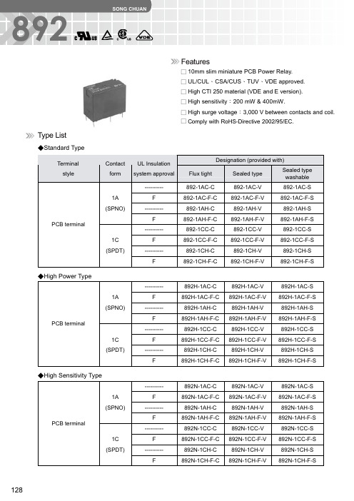
892松川系列继电器

30G
Damage limits
100G
Mechanical
10,000,000 operations (frequency 1800 operations/hr)
Electrical
100,000 operations (frequency 900 operations/hr)
-40 ~ +85℃ (no freezing)
10A/5A 125VAC
5A/3A 277VAC
7A/5A 277VAC
TV-3
TUV Pending
TUV
892
892H
7A/3A 120VAC 5A/3A 240VAC
10A/5A 120VAC 7A/5A 240VAC
277VAC NC / NO:1200VA/1680VA
892
COIL DATA (Standard type)
Rated current Coil resistance
Max.
Pickup voltage Dropout voltage Power
Rated voltage ±10% at 25℃ ±10% at 25℃ continuous
36
5.6
6480
SPECIFICATION
Contact resistance Operate time Release time Insulation resistance
Dielectric strength (initial value) Vibration resistance
Shock resistance
3 Blank-Standard type
1CC-SPDT Contact material AgNi10
综合测试仪HP8920/21操作快速入门
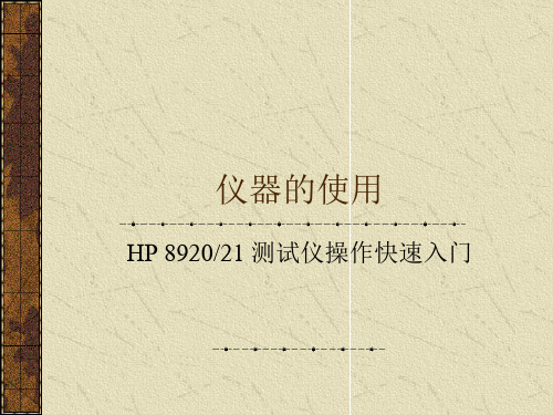
如何使用频谱分析仪观测信号
在“To Screen”下选择SPEC ANL进入 SPECTRUM ANALYZER 在“Controls”下选择相应的输入端口RF In/Ant 在“Center Freq”下设置待测的中心频率 根据带测的信号功率在“Ref Level”下设 置合适的参考功率 在“Span”下设置水平显示范围
如何建立一个带信令的单音调制信号
建立一个单音调制信号 在“To Screen”下选择“ENCODER”设置 好要求的信令(在信令那一节会详细讲 述) 按下按键“PREV”回到RX TEST界面 在“AFGen2”下选择Send/Stop; 即可实现带信令的单音调制信号的发生与 关闭
如何建立一个两音调制信号
如何选择示波器输入
在“To Screen”下选择SCOPE可进入示波器界面 选择示波器输入方式需在“To Screen”下选择AF ANL进入AF Analyzer 在“AF Anl In”下选择正确的音频输入方式 在面板上按下按键PREV重新进入示波器界面 常用两种方式: FM Demod:调频解调音频输入 Audio In:音频端口输入
如何测量载波频率及频率误差
在“Tune Mode”下选择Auto 连接端口后发射测量信号 在“TX Frequency”下将显示载波信号的频 率 在“Tune Mode”下选择Manual 在“Tune Freq”下设定解调频率 在“TX Freq Error”将显示频率误差
如何选择射频输入端口
RX Test And RF Generator
如何建立一个单音调制信号 如何建立一个带信令的单音调制信号 如何建立一个两音调制信号 如何选择射频输出端口
Agilent8920

Agilent8920/8921通信测试仪(综测)使用说明一、仪器面板键盘操作及菜单1、面板CRT显示●RX TEST—接收机测试屏幕,可显示RF和AF控制及接收机测试结果。
●TX TEST—发射机测试屏幕,可显示RF和AF控制及发射机测试结果。
●DUPLEX TEST—双工测试屏幕,可同时显示RF和AF控制及收发信机测试结果。
●TESTS—访问来自存储卡、内部ROM/RAM及外接磁盘驱动器装入的程序,可对其编辑与自动运行的屏幕,显示测试结果。
●RF GENERATOR—射频信号源屏幕,用于显示射频与调制信号的控制及测试结果。
●RF ANAL YZER—射频分析仪屏幕,用于显示射频与解调信号的控制及测试结果。
●AF ANAL YZER—音频分析仪屏幕,用于显示音频信号的控制与测试结果。
●OSCILLOSCOPE—示波器屏幕,用于完成对示波器的控制及显示测量结果。
●SPECTRUM ANAL YZER—频谱分析仪屏幕。
●SIGNALING ENCODER—信令编码器屏幕。
●SIGNALING DECODER—信令解码器屏幕。
●RADIO INT—无线电接口与屏幕,显示仪器内置无线电接口卡对外接模块与设备的自动测试结果。
2、面板连接器与控制器●POWER—仪器的电源开关键。
●RF IN/OUT连接器—是一阻抗为50Ω的N型阴性插座,用作射频信号源的输出与调制分析仪的输入接口,允许连续输入60W,或输入100W功率。
●DUPLEX OUT连接器—是一阻抗为50Ω的BNC型阴性插座,用作射频信号源及跟踪信号源的输出端口。
●ANT IN连接器—用作小功率射频信号(≤200Mw)及空中信号的输入端口。
●MIC/ACC接口—是一8针DIN接口,可提供多种用途的连接:MIC IN—当KEY IN接地时去调制射频发生器(先滤波与放大);KEY IN—用于射频信号源的输出开/关状态控制,及在TX TEST与RX TEST屏幕之间的转换控制;KEY OUT1与KEY OUT2用于一部外设的开/关控制。
892H-1CC-C(松川)
3
66.7
5
40.0
6
33.3
9
22.2
45 80 % of ratHale Waihona Puke d125voltage
180
170 % of
(HN type or
5 % of
1C type only)
405
rated
rated
approx. 0.2W
12
16.7
720
voltage
75 % of
voltage
18
11.1
1620
Dielectric strength (1)
Between open contact : AC 1000V , 50/60Hz 1 min. Between contact and coil : AC 4000V , 50/60Hz 1 min.
Vibration resistance
Operating extremes Damage limit
VDE 40006318
UL / CUL E88991
130
SONG CHUAN
892
Safety Approval Rating
CSA / CUS
892
892H
NOΚ7A 125VAC
NOΚ10A 125VAC
5A 277VAC
7A 277VAC
NCΚ3A 125VAC
TV-3
3A 277VAC
128
SONG CHUAN
本页已使用福昕阅读器进行编辑。
892 福昕软件(C)2005-2007,版权所有,
仅供试用。
Ordering Information
TDA8924中文资料
INTEGRATED CIRCUITS
DATA SHEET
TDA8924 2 × 120 W class-D power amplifier
Objective specification 2003 Jul 28
元器件交易网
Philips Semiconductors
TDA8924
DYNAMIC AC CHARACTERISTICS (MONO BTL APPLICATION) APPLICATION INFORMATION BTL application Pin MODE Output power estimation External clock Heatsink requirements Output current limiting Pumping effects Reference design PCB information for HSOP24 encapsulation Classification Reference design: bill of materials Curves measured in the reference design PACKAGE OUTLINE SOLDERING Introduction to soldering surface mount packages Reflow soldering Wave soldering Manual soldering Suitability of surface mount IC packages for wave and reflow soldering methods DATA SHEET STATUS DEFINITIONS DISCLAIMERS
6 BLOCK DIAGRAM
2SB892S-AE中文资料(sanyo)中文数据手册「EasyDatasheet - 矽搜」
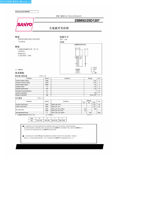
10
12
ITR08649
2SD1207 VCE=2V
800
600
集电4极00电流,IC - 毫安
200
0
0
0.2
0.4
0.6
0.8
1.0
1.2
基极 - 发射极电压,VBE - V
ITR08651
No.930–2/4
芯片中文手册,看全文,戳
2SB892/2SD1207
hFE -- IC
PS No.930–4/4
10 --10
2
100 7 5
2 3 5 7 --100 2 3 5 7 --1000 2 3
集电极电流,IC - 毫安
ITR08654
柯布 - VCB
2SB892 f=1MHz
3
2
输出电容,科夫 - pF
10
7 5 --1.0
--100 5 2
--10 5
2 3 5 7 --10
2
集电极 - 基极电压VCB - V
--200
0
0
--0.2
--0.4
--0.6
--0.8
--1.0
--1.2
基极 - 发射极电压,VBE - V
ITR08650
IC -- VCE
2.4
50mA
2.0
40mA
25mA
1.6
1.2
集电极电流,IC - 一个
0.8
15mA 8mA 4mA
0.4
2mA
2SD1207
0 0 1200 1000 800
三洋承担所造成产品使用AT超越,即使是瞬间值,设备故障不承担任何责任,额定数值(例如最大 额定值,工作环境范围或其他参数)任何产品规格及所有SANYO产品描述或此处包含上市.
2.4G芯片 升级版LT8920 数据手册

Page 2
2013 年 6 月
LT8920 中文手册 1.0
9.22. Register 42................................ ........................ 25
9.23. Register 43................................ ........................ 25
6.1. SPI 默认格式 ................................ ........................ 12 6.2. SPI Optional Format................................ ................... 12 6.3. SPI 时序要求 ................................ ........................ 12 7. IIC 接口 ................................ ............................. 14 7.1. I2C 命令格式 ................................ ........................ 14 7.2. I2C 特性................................ ............................ 14 7.3. I2C 器件地址 ................................ ........................ 15 8. 状态机框图................................ ............................ 16 9. 寄存器信息................................ ............................ 17 9.1. Register 3 – Read only ................................ ............... 17 9.2. Register 6 – Read only ................................ ............... 17 9.3. Register 7 ................................ .......................... 17 9.4. Register 9 ................................ .......................... 18 9.5. Register 10 ................................ ......................... 18 9.6. Register 11 ................................ ......................... 18 9.7. Register 23 ................................ ......................... 18
Whelen 14544 (111411) ligt 高压 燃烧防护 盒部件 中文名称说明书
©2011 Whelen Engineering Company Inc.Form No.14544 (111411)For warranty information regarding this product, visit /warranty•Proper installation of this product requires the installer to have a good understanding of automotive electronics, systems and procedures.•Whelen Engineering requires the use of waterproof butt splices and/or connectors if that connector could be exposed to moisture.•Any holes, either created or utilized by this product, should be made both air- and watertight using a sealant recommended by your vehicle manufacturer.•Failure to use specified installation parts and/or hardware will void the product warranty.•If mounting this product requires drilling holes, the installer MUST be sure that no vehicle components or other vital parts could be damaged by the drilling process. Check both sides of the mounting surface before drilling begins. Also de-burr the holes and remove any metal shards or remnants. Install grommets into all wire passage holes.•If this manual states that this product may be mounted with suction cups, magnets, tape or Velcro®, clean the mounting surface with a 50/50 mix of isopropyl alcohol and water and dry thoroughly.•Do not install this product or route any wires in the deployment area of your air bag. Equipment mounted or located in the air bag deployment area will damage or reduce the effectiveness of the air bag, or become a projectile that could cause serious personal injury or death. Refer to your vehicle owner’s manual for the air bag deployment area. The User/Installer assumes full responsibility to determine proper mounting location, based on providing ultimate safety to all passengers inside the vehicle.•For this product to operate at optimum efficiency, a good electrical connection to chassis ground must be made. The recommendedprocedure requires the product ground wire to be connected directly to the NEGATIVE (-) battery post (this does not include products that use cigar power cords).•If this product uses a remote device for activation or control, make sure that this device is located in an area that allows both the vehicle and the device to be operated safely in any driving condition.•Do not attempt to activate or control this device in a hazardous driving situation.•This product contains either strobe light(s), halogen light(s), high-intensity LEDs or a combination of these lights. Do not stare directly into these lights. Momentary blindness and/or eye damage could result.•Use only soap and water to clean the outer lens. Use of other chemicals could result in premature lens cracking (crazing) and discoloration. Lenses in this condition have significantly reduced effectiveness and should be replaced immediately. Inspect and operate this product regularly to confirm its proper operation and mounting condition. Do not use a pressure washer to clean this product.•It is recommended that these instructions be stored in a safe place and referred to when performing maintenance and/or reinstallation of this product.•FAILURE TO FOLLOW THESE SAFETY PRECAUTIONS AND INSTRUCTIONS COULD RESULT IN DAMAGE TO THE PRODUCT OR VEHICLE AND/OR SERIOUS INJURY TO YOU AND YOUR PASSENGERS!A u t o m o t i v e : Warnings to InstallersWhelen’s emergency vehicle warning devices must be properly mounted and wired in order to be effective and safe. Read and follow all of Whelen’s written instructions when installing or using this device. Emergency vehicles are often operated under high speed stressful conditions which must be accounted for when installing all emergency warning devices. Controls should be placed within convenient reach of the operator so that they can operate the system without taking their eyes off the roadway. Emergency warning devices can require high electrical voltages and/or currents. Properly protect and use caution around live electrical connections.Grounding or shorting of electrical connections can cause high current arcing, which can cause personal injury and/or vehicle damage, including fire. Many electronic devices used in emergency vehicles can create or be affected by electromagnetic interference. Therefore, after installation of any electronic device it is necessary to test all electronic equipment simultaneously to insure that they operate free of interference from other components within the vehicle. Never power emergency warning equipment from the same circuit or share the same grounding circuit with radio communication equipment. All devices should be mounted in accordance with the manufacturer’s instructions and securely fastened to vehicle elements of sufficient strength to withstand the forces applied to the device. Driver and/or passenger air bags (SRS) will affect the way equipment should be mounted. This device should be mounted by permanent installation and within the zones specified by the vehicle manufacturer, if any. Any device mounted in the deployment area of an air bag will damage or reduce the effectiveness of the air bag and may damage or dislodge the device. Installer must be sure that this device, its mounting hardware and electrical supply wiring does not interfere with the air bag or the SRS wiring or sensors. Mounting the unit inside the vehicle by a method other than permanent installation is not recommended as unit may become dislodged during swerving; sudden braking or collision. Failure to follow instructions can result in personal injury. Whelen assumes no liability for any loss resulting from the use of this warning device. PROPER INSTALLATION COMBINED WITH OPERATOR TRAINING IN THE PROPER USE OF EMERGENCY WARNING DEVICES IS ESSENTIAL TO INSURE THE SAFETY OF EMERGENCY PERSONNEL AND THE PUBLIC.Warnings to UsersWhelen’s emergency vehicle warning devices are intended to alert other operators and pedestrians to the presence and operation of emergency vehicles and personnel. However, the use of this or any other Whelen emergency warning device does not guarantee that you will have the right-of-way or that other drivers and pedestrians will properly heed an emergency warning signal. Never assume you have the right-of-way. It is your responsibility to proceed safely before entering an intersection, driving against traffic, responding at a high rate of speed, or walking on or around traffic lanes. Emergency vehicle warning devices should be tested on a daily basis to ensure that they operate properly. When in actual use, the operator must ensure that both visual and audible warnings are not blocked by vehicle components (i.e.: open trunks or compartment doors), people, vehicles, or other obstructions. It is the user’s responsibility to understand and obey all laws regarding emergency warning devices. The user should be familiar with all applicable laws and regulations prior to the use of any emergency vehicle warning device. Whelen’s audible warning devices are designed to project sound in a forward direction away from the vehicle occupants. However, because sustained periodic exposure to loud sounds can cause hearing loss, all audible warning devices should be installed and operated in accordance with the standards established by the National Fire Protection Association.Safety FirstThis document provides all the necessary information to allow your Whelen product to be properly and safely installed. Before beginning the installation and/or operation of your new product, the installation technician and operator must read this manual completely. Important information is contained herein that could prevent serious injury or damage.WARNING: This product can expose you to chemicals including Methylene Chloride which is known to the State of California to cause cancer, and Bisphenol A, which is known to the State of California to cause birth defects or other reproductive harm. For more information go to .Installation Guide:Inner Edge® Traffic Advisor™ Series Lo-Profile Rear Deck Interior Lightbar2011 Dodge Charger51 Winthrop RoadChester, Connecticut 06412-0684Phone: (860) 526-9504Internet: Salese-mail:*******************CustomerServicee-mail:*******************®ENGINEERING COMPANY INC.IMPORTANT!Do not install this product or route any wires in the air bag deployment zone of your vehicle. Equipment mounted or located in air bag deployment zones will damage or reduce the effectiveness of the air bag, or become a projectile that could cause serious personal injury or death. Refer to your vehicle owners manual to learn the air bag deployment zones for the vehicle. The User/Installer assumes full responsibility to determine proper mounting location, based on providing ultimate safety to all passengers inside the vehicle.Installation:IMPORTANT! The lightbar should be located a minimum of 16" from any radio antennas!1.On the rear deck, locate the driver-side outboard cap covering the childrestraint strap holder. Remove this cover to access the tether strap holder.2.For the next step you must remove the plastic panel located inside thetrunk to access the bottom side of the child restraint brackets. This panel is held on with christmas tree plugs and magnets.3.Locate the driver-side lightbar mounting bracket included with themounting kit. Secure the mounting bracket onto the strap holder using the hardware shown (Fig. 1). Tighten the hardware firmly.4.Repeat steps 1 thru 3 for the Passenger-side mounting bracket thenreplace the plastic panel you removed in step 2.5.Position the lightbar onto the rear deck. Secure the lightbar to themounting brackets using the hardware shown. Do not tighten this hardware yet.Make sure that the rubber window seal on the lightbar housing fully engages the rear window. To ensure this, hold the lightbar housing firmly against the glass while tightening the hardware securing lightbar to mounting bracket.While still maintaining pressure on the lightbar, tighten the hardware used to secure lightbar mounting bracket to the child restraint holder.The lightbar should maintain the seal against the windshield when the pressure is released. If not, loosen the appropriate hardware and repeat this tightening procedure until properly mounted.6.Route the input cable to your control head (refer to the installation manualincluded with your control head for important mounting and wiring information).IMPORTANT!When routing the lightbar cable, it is left to the installation technician's discretion to select a path for these cables that will both protect the cables from possible damage and not interfere with the operation of any other vehicle components or equipment. Refer to the instructions included with your switches for switch wiring information.Wiring and Operation:WARNING!All customer supplied wires that connect to the positive terminal of the battery must be sized to supply at least 125% of the maximum operating current and FUSED at the battery to carry that load. DO NOT USE CIRCUIT BREAKERS WITH THIS PRODUCT!BLACK - GroundExtend and connect the BLK wire to the ground terminal of the vehicle battery. RED - Main PowerRoute the RED wire to an unused, ignition-controlled circuit fused @ 10 Amps. Do not connect to this circuit yet.NOTE: When this product is wired as outlined here, the lightbar will not function until the ignition switch is in the ON, RUN or ACC position.WHT-ORG - Scan-Lock™ Flash patternsWhen the TA feature is active, this wire will select TA patterns; when the end flasher feature is active, this wire will select the end flasher patterns. Do not use Scan-Lock while both features are simultaneously active.TO CYCLE THROUGH ALL PATTERNS: Apply +12 volts to the WHT/ ORG wire for less than 1 second and release to cycle forward. Apply +12 volts for more than 1 second and release to cycle backward.TO SET A PATTERN AS DEFAULT: When the desired pattern is displayed, allow it to run for more than 5 seconds. The TA will now displaythis pattern when active.TO RESET TO THE FACTORY DEFAULT PATTERN: Turn off power, apply +12 volts to the WHT/ORG wire, then turn power on.A Normally Open Momentary Switch is best for this circuit. Fuse @1A.Scan-Lock End Flasher Patterns:1. SignalAlert™ 4. SingleFlash 752. CometFlash® 5. ActionFlash™3. SingleFlash 375 6. A ctionScan™Traffic Advisor Patterns:1. Sequence to Solid 3. 1-Lamp TripleFlash™2. Seq. On/Seq. Off 4. 2-Lamp TripleFlashWHT/GRN - Low Power OperationFor low power operation apply +12VDC to the WHT/GRN wire. The unit will continue to operate in Low Power mode until this voltage is removed.A SP/ST switch is best suited for this circuit. Fuse this wire @1A. BROWN - End FlashersApplying +12VDC to this wire activates the end flashers. A SP/ST switch is best suited for this circuit. Fuse this wire @1A.BLUE - TA FlashWhen +12VDC is applied to this wire, the Traffic Advisor™ lightbar function becomes active. A SP/ST switch is best suited for this circuit. Fuse this wire @1A.ORANGE - LeftWhen +12VDC is applied to this wire, the lights sweep from right to left. A SP/ST switch is best suited for this circuit. Fuse this wire @1A.WHITE/BLACK - RightWhen +12VDC is applied to this wire, the lights sweep from left to right. A SP/ST switch is best suited for this circuit. Fuse this wire @1A.NOTE: If you apply power to both the WHT/BLK and ORG wires simultaneously, you will get a split pattern. Both sides will start at the center and sweep outward.。
?HS2-9-1德国料号:1.3346
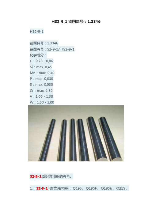
HS2-9-1德国料号:1.3346HS2-9-1德国料号:1.3346德国牌号:S2-9-1/ HS2-9-1化学成分:C:0,78 - 0,86Si:max. 0,45Mn:max. 0,40P:max. 0,030S:max. 0,030Cr:max. 1,50V:1,00 - 1,30W:1,50 - 2,00S2-9-1部分常用钢的牌号。
1、S2-9-1碳素结构钢:Q195、Q195F、Q195b、Q215、Q215AF、Q215Ab、Q215A、Q215BF、Q215Bb、Q215B、Q235、Q235AF、Q235Ab、Q235A、Q235BF、Q235Bb、Q235B、Q235C、Q235D、Q255、Q255A、Q255B、Q275、Q2752、S2-9-1通用低合金高强度结构钢:Q295、Q295A、Q295B、Q345、Q345A、Q345B、Q345C、Q345D、Q345E、Q390、Q390A、Q390B、Q390C、Q390D、Q390E、Q420、Q420A、Q420B、Q420C、Q420D、Q420E、Q460、Q460C、Q460D、Q460E3、S2-9-1低合金高强度结构钢:一般采用代表屈服点的拼音字母“Q”、屈服点数值(单位为MPa) 、并在尾部加按产品用途的拼音个字母表示。
如:压力容器用钢牌号表示为“Q345R” ;焊接气瓶用钢牌号表示为“Q295HP”;锅炉用钢牌号表示为“Q390g”;桥梁用钢牌号表示为“Q420q”等。
4、S2-9-1优质碳素结构钢:08F、10F、15F、08、10、15、20、25、30、35、40、45、50、55、60、65、70、75、80 、85、15Mn、20Mn、25Mn、30Mn、35Mn、40Mn、45Mn、50Mn、60Mn、65Mn、70Mn共31个5、S2-9-1易切削结构钢:易切削结构钢分加易切削钢、加易切削钢、加铅易切削钢、加钙易切削钢、加碳锰易切削钢等。
Chemlok 289 290 胶合剂技术数据表说明书

Chemlok® 289/290 Adhesive Technical Data SheetChemlok® 289/290 adhesive is an adhesive system designed for bonding rubber linings to steel, stainless steel, aluminum, titanium, wood and other substrates. It is composed of a mixture of polymers, organic compounds and mineral fillers dissolved or dispersed in an organic solvent system.Chemlok 289/290 adhesive is suitable for cure by autoclave, open steam or chemical techniques. Features and Benefits:Versatile – bonds many rubber compounds to a variety of substrates.Easy to Apply – applies easily by brush, roll coat or spray methods.Corrosion Resistant – provides excellent corrosion resistance.Application:Surface Preparation – Thoroughly clean metal surfaces prior to primer application. Remove protective oils, cutting oils and greases by solvent degreasing or alkaline cleaning. Remove rust, scale or oxide coatingsby grit blasting. Use steel grit to blast clean steel and other ferrous metals. Use aluminum oxide, sand or other nonferrous grit to blast clean stainless steel, aluminum and other nonferrous metals.For further detailed information on surface preparationof specific substrates, refer to Chemlok Adhesives application guide.Mixing – Thoroughly stir primer and covercoat before use, and agitate sufficiently during use to keep dispersed solids uniformly suspended.Chemlok 289 primer and Chemlok 290 covercoatare normally used full strength for brush or roll coat applications. For spray application, dilute Chemlok 289 primer with a 1:1 MEK/xylene mixture; dilute Chemlok 290covercoat with xylene or toluene.Applying – Separately apply primer and covercoat by brush, roll coat or spray methods. For best results, apply adhesive system to surfaces with temperatures less than 38°C (100°F).Regardless of application method, the recommended dry film thickness ranges are:Chemlok 289 10.2-22.9 micron (0.4-0.9 mil) Chemlok 290 2.5-15.2 micron (0.1-0.6 mil) Optimal dry film thicknesses of primer and covercoat vary based on the end-use application (i.e., substrate, elastomer, application method, cure method, service environment, etc.).Drying/Curing – Allow primer to air-dry for 30-60 minutes before applying covercoat to prevent solvent entrapment and subsequent blistering.If parts applied with Chemlok 289 primer remain uncoated for more than seven days, primer must be reapplied prior to Chemlok 290 covercoat application. Parts coatedwith Chemlok 290 covercoat can be stored for up to seven days prior to rubber layup without affecting bond performance if protected from sunlight exposure. Cleanup – Use xylene, toluene or MEK for clean up. Shelf Life/Storage:Shelf life is one year from date of shipment when stored by the recipient in a well ventilated area at 21-27°C (70-80°F) in original, unopened container. Store container in a dry location, away from sunlight. Keep container closed when not in use.Cautionary Information:Before using this or any Parker LORD product, refer to the Safety Data Sheet (SDS) and label for safe use and handling instructions.For industrial/commercial use only. Must be applied by trained personnel only. Not to be used in household applications. Not for consumer use.Parker LORDEngineered Materials Group 111 LORD DriveCary, NC 27511-7923USAphone +1 877 ASK LORD (275 5673)Values stated in this document represent typical values as not all tests are run on each lot of material produced. For formalized product specifications for specific product end uses, contact the Customer Support Center.Information provided herein is based upon tests believed to be reliable. In as much as Parker LORD has no control over the manner in which others may use this information, it does not guarantee the results to be obtained. In addition, Parker LORD does not guarantee the performance of the product or the results obtained from the use of the product or this information where the product has been repackaged by any third party, including but not limited to any product end-user. Nor does the company make any express or implied warranty of merchantability or fitness for a particular purpose concerning the effects or results of such use.WARNING — USER RESPONSIBILITY . FAILURE OR IMPROPER SELECTION OR IMPROPER USE OF THE PRODUCTS DESCRIBED HEREIN OR RELATED ITEMS CAN CAUSE DEATH, PERSONAL INJURY AND PROPERTY DAMAGE.This document and other information from Parker-Hannifin Corporation, its subsidiaries and authorized distributors provide product or system options for further investigation by users having technical expertise.The user, through its own analysis and testing, is solely responsible for making the final selection of the system and components and assuring that all performance, endurance, maintenance, safety and warning requirements of theapplication are met. The user must analyze all aspects of the application, follow applicable industry standards, and follow the information concerning the product in the current product catalog and in any other materials provided from Parker or its subsidiaries or authorized distributors.To the extent that Parker or its subsidiaries or authorized distributors provide component or system options based upon data or specifications provided by the user, the user is responsible for determining that such data and specifications are suitable and sufficient for all applications and reasonably foreseeable uses of the components or systems.©2022 Parker Hannifin - All Rights ReservedInformation and specifications subject to change without notice and without liability therefor. Trademarks used herein are the property of their respective owners.OD DS3137 07/22 Rev.5。
WKH-892馈线

I
2 S
+
I
2 C
(1)
X = VC IS − VSIC
I
2 S
+
I
2 C
其中:VS、VC—基波电压正弦、余弦分量; IS、IC—基波电流正弦、余弦分量; R、X—测量电阻和电抗。
对于 AT 供电方式,电流为 T 线、F 线电流差的一半,即 &I = (&It − &If )/2 ,电压 U& 为母
114
I2 、 I3 、 I5 ─当前二、三、五次谐波电流;
I
' 2
、
I3'
、
I
' 5
─
一周波前二、三、五次谐波电流;
K h ─谐波加权抑制系数;
2
ΔIZD ─电流增量保护整定值;
K YL ─二次谐波闭锁整定值。
c)实现框图
图 5.5-5 电流增量保护原理框图
5.5 反时限过负荷保护 本装置设反时限过负荷保护。当接触网因长期大电流发热达到一定程度时应跳开馈
245.9
4-φ6.5
241.6 259.2
图 5.4-1 装置外形尺寸图
227 +00.5 241.6±0.2
图 5.4-2 装置开孔尺寸图
112
5 保护原理
5.1 自适应距离保护 ·动作特性:如图 5.5-1 所示。
X
2
XZD
φ1
φL
R
φ2
RZD
图 5.5-1 距离保护动作特性
·测量阻抗计算
R = VSIS + VC IC
●在额定电流、线路阻抗角及电压范围 0.5~120V 条件下,动作误差不超过±5%,
富士豪低温螺杆目录
Frascold于75年前创立并展望未来。
利用我们的技术,应用经验和全球业务;我们供应 产品,解决方案和服务,也为客户提供了性能,能 源效率和操作舒适性方面的优势。
我们的压缩机用于众多冷冻,空调与热泵行业,影 响了无数人的日常生活。
2
Blue is better
Refrigeration Twin Screw Compressors 冷冻双螺杆压缩机
Frascold is a manufacturing company that operates world-wide, bringing experience, resources, technology and highly-skilled personnel to all of its activity. Frascold has the tools to provide proximity and act quickly in response to market needs, and is looking confidently to its future.
Characteristics The accurate design, the entirely made in Italy production, the methodical total quality controls, guarantee excellent performance and reliability. The wide range of models is divided in three distinct versions due to their ideal optimization for different applications: • RTSL / NRL models designed for low evaporating
- 1、下载文档前请自行甄别文档内容的完整性,平台不提供额外的编辑、内容补充、找答案等附加服务。
- 2、"仅部分预览"的文档,不可在线预览部分如存在完整性等问题,可反馈申请退款(可完整预览的文档不适用该条件!)。
- 3、如文档侵犯您的权益,请联系客服反馈,我们会尽快为您处理(人工客服工作时间:9:00-18:30)。
mpl
L?KOCL?>g JF?;M?=IHN;=N OM i
?:4
FH7A>B>6GHE:>BG:EA:9>6G:DCJ:E E:@6K
8CBG68G 96G6
d
d 4CHAF?MC>?MN;<F?
l =ICF F;N=BCHA m =ICFM F;N=BCHA
nkk G8lpk G8nkk G8
z ICF JIQ?L
8C>@
m m m +@NB?;G<C?H=?;FFIQM g @FORJLI I @?>CM JL?@?L?HNC;FFS L?=I GG?H>?>i
me ,|s CM ;H ?HPCLIHG?HN;F @LC?H>FS JLI>O=N i 1F?;M?G;LE ;MJ?=C;F =I>?dpppe QB?H IL>?LCHA i
4CHAF?MC>?MN;<F?c l =ICF F;N=BCHA
m =ICFM F;N=BCHA
mpm
0ONFCH?{CG?HMCIHM
CHG@>B:9>A:BF>CBF.J>E>B<9>6<E6A 6B9D87C6E9@6KCHG
6HCN u GG
{CM=F;CG?L
5BCM >;N;MB??N CM @IL NB?=OMNIG?LMX L?@?L?H=?i x FF NB?MJ?=C@C=;NCIHM ;L?MO<D?=N NI =B;HA?QCNBION HINC=?i
8?=IOF>HIN ?P;FO;N?;FF NB?J?L@ILG;H=?;H>;FF NB?J;L;G?N?LM @IL ?P?LS JIMMC<F?;JJFC=;NCIH i 5BOM NB?OM?L MBIOF><?CH ;LCABN JIMCNCIH NI =BIIM?NB?MOCN;<F?JLI>O=N @IL NB?CL IQH ;JJFC=;NCIH i +@NB?L?CM ;HS KO?LS g JF?;M?=IHN;=N *IHA@;@IL NB?N?=BHC=;F M?LPC=?i *IQ?P?L g CN CM NB?OM?LXM L?MJIHMC<CFCNS NI >?N?LGCH?QBC=B JLI>O=N MBIOF><?OM?>IHFS i
U 9C;G?H *IHA@;|F?=NLI;=IOMNC=z I ig -N>i x FF LCABNM I@*IHA@;;L?L?M?LP?>i
4CHAF?MC>?MN;<F?c l =ICF F;N=BCHA
m =ICFM F;N=BCHA
l }ILG x
4CHAF?MC>?MN;<F?d{??H?LACT?>=IH>CNCIH e
m =ICFM
l =ICF l }ILG x
m }ILG x
lx f ly
BX\TNP
li 3?F;S CM IH NB?YL?M?NZ MN;NOM QB?H <?CHA L?F?;M?>@LIG MNI=E g QCNB NB?=IHMC>?L;NCIH I@MBI=E LCM?H @LIG NL;HMCN ;H>L?F;S GIOHNCHA g L?F;S QIOF><?=B;HA?>NI YM?NZ MN;NOM g NB?L?@IL?g QB?H ;JJFC=;NCIH d =IHH?=NCHA NB?JIQ?L MOJJFS eg JF?;M?L?M?N NB?L?F;S NI YM?NZ IL YL?M?NZ MN;NOM IH L?KO?MN i
mi +H IL>?L NI G;CHN;CH YM?NZ IL YL?M?NZ MN;NOM g ?H?LACT?>PIFN;A?NI =ICF MBIOF>L?;=B NB?L;N?>PIFN;A?g CGJOFM?QC>NB MBIOF><?p NCG?M GIL?NB;H YM?NZ IL YL?M?NZ NCG?i {I HIN ?H?LACT?PIFN;A?NI YM?NZ =ICF ;H>YL?M?NZ =ICF MCGOFN;H?IOMFS i x H>;FMI FIHA ?H?LACT?>NCG?d GIL?NB;H l GCH e MBIOF><?;PIC>?>i
ni +H IL>?L NI ;PIC>=B;HACHA IJ?L;N?PIFN;A?g JLI>O=NM MBIOF>HIN <?E?JN CH MNLIHA G;AH?NC=@C?F>>OLCHA NL;HMJILN;NCIH g MNIL;A?;H>;JJFC=;NCIH i
3?G;LE u le +H =;M?I@HI NIF?L;H=?MBIQH CH IONFCH?>CG?HMCIH u IONFCH?>CG?HMCIH ^l GG g NIF?L;H=?MBIOF><?V kim GG v IONFCH?>CG?HMCIH a l GG
;H>^p GG g NIF?L;H=?MBIOF><?V kin GG v IONFCH?>CG?HMCIH a p GG g NIF?L;H=?MBIOF><?V kio GG i me 5B?NIF?L;H=?QCNBION CH>C=;NCHA @IL 1zy F;SION CM ;FQ;SM V kil GG i ne 5B?QC>NB I@NB?ALC>>CHA CM mipo GG i
mpn
dy INNIG PC?Q e
CHG@>B:9>A:BF>CBF.J>E>B<9>6<E6A 6B9D87C6E9@6KCHG
6HCN u GG
1zy -;SION
8CLCHA {C;AL;G
dy INNIG PC?Q e
l }ILG x
m }ILG xg lx f ly m }ILG xg lx f ly。
