BSS89E6296中文资料
89E516RD中文
5
e-mail: szks@
深圳市科赛科技开发有限公司 0755-83000297 13316986132
P3[5]
I
T1:定时器 1 外部输入
P3[6]
O
WR#:外部数据存储器写信号
P3[7]
O
RD#:外部数据存储器读信号
PSEN#
I/O
程序存储使能。是对外部程序的读选通脉冲,当执行内部程序
深圳市科赛科技开发有限公司 0755-83000297 13316986132
SST89E52RD2 / SST89E54RD2 / SST89E58RD2 /SST89E516RD2 SST89V52RD2 / SST89V54RD2 / SST89V58RD2 /SST89V516RD2
2
e-mail: szks@
深圳市科赛科技开发有限公司 0755-83000297 13316986132 1.0 功能方框图
3
e-mail: szks@
深圳市科赛科技开发有限公司 0755-83000297 13316986132 2.0 引脚定义图
ALE 脉冲将被忽略。ALE 可以通过置位 SFR 的 Auxlilary.0 禁
止,置位后 ALE 只能在执行 MOVX 指令时被激活。
P4[3:0]5
I/O
Port4:P4 是带内部上拉的 4 位双向 I/O 口。P4 的输出可以驱
ES569_TDS
The information given and the recommendations made herein are based on our research and are believed to be accurate but no guarantee of their accuracy is made. In every case we urge and recommend that purchasers before using any product in full-scale production make their own tests to determine to their own satisfaction whether the product is of acceptable quality and is suitable for their particular purpose under their own operating conditions. THE PRODUCTS DISCLOSED HEREIN ARE SOLD WITHOUT ANY WARRANTY AS TO MERCHANTABILITY OR FITNESS FOR A PARTICULAR PURPOSE OR ANY OTHER WARRANTY, EXPRESS OR IMPLIED.No representative of ours has any authority to waive or change the foregoing provisions but, subject to such provisions, our engineers are available to assist purchasers in adapting our productsFeatures & BenefitsExcellent adhesive strengthExcellent resistance to vibration Easy to use –no mixing requiredHigh shear and peel strengthHigh temperature resistanceGood resistance to chemicalsNon-sag, thixotropicDescriptionPERMABOND® ES569 is a single-part heat cured epoxy adhesive with excellent adhesion to metal surfaces as well as composite materials. The high bond strength of this adhesive allows it to replace mechanical fastening,soldering, brazing or welding. ES569 has been designed to be non-sagging, allowing the product to be used in large gaps and on vertical surfaces. It is also ideal for bonding electronic components as it has high wet strength and is non-stringing and produces an excellent drop profile as well as withstanding solder reflow processes.Physical Properties of Uncured AdhesiveTypical Curing Propertiesadhesive to reach this temperature - for example, largeassemblies or a crowded oven will require longer to reach full cure. Alternative, quicker methods of curing include induction, hotplates, infrared lamps and hot-air guns.Typical Performance of Cured Adhesivepreparation and gap.PERMABOND® ES569Single-part, heat-cure EpoxyTechnical DatasheetThe information given and the recommendations made herein are based on our research and are believed to be accurate but no guarantee of their accuracy is made. In every case we urge and recommend that purchasers before using any product in full-scale production make their own tests to determine to their own satisfaction whether the product is of acceptable quality and is suitable for their particular purpose under their own operating conditions. THE PRODUCTS DISCLOSED HEREIN ARE SOLD WITHOUT ANY WARRANTY AS TO MERCHANTABILITY OR FITNESS FOR A PARTICULAR PURPOSE OR ANY OTHER WARRANTY, EXPRESS OR IMPLIED.No representative of ours has any authority to waive or change the foregoing provisions but, subject to such provisions, our engineers are available to assist purchasers in adapting our productsAdditional InformationThis product is not recommended for use in contact with strong oxidizing materials.Information regarding the safe handling of this material may be obtained from the material safety data sheet (MSDS).Users are reminded that all materials, whether innocuous or not, should be handled in accordance with the principles of good industrial hygiene.Surface PreparationSurfaces should be clean, dry and grease-free before applying the adhesive. Use a suitable solvent (such as acetone or isopropanol) for the degreasing of surfaces. Some metals such as aluminium, copper and its alloys will benefit from light abrasion with emery cloth (or similar), to remove the oxide layer.Directions for Use1) The adhesive should be dispensed from thecartridge via the nozzle supplied (this can be cut to give the appropriate sized bead to cover the bond area).2) Apply the adhesive to one surface and avoidentrapping air.3) Assemble parts applying sufficient pressure toensure the adhesive spreads to cover the entire bond area.4) Use a jig / clamp to prevent parts moving duringcure.5) It is advisable not to disturb the joint until theadhesive is fully cured.6) Cure with heat – see page one for cure schedule.Storage & HandlingContact Permabond:• Americas +1 732 868 1372• US 800-640-7599 • Asia + 86 21 5773 4913 • Europe +44 (0) 1962 711661• UK 0800 975 9800• Deutschland 0800 111 388• France 0805 111 388info.americas@ info.europe@ @。
2SA966资料

TOSHIBA Transistor Silicon PNP Epitaxial Type (PCT Process)2SA966Audio Power Amplifier Applications• Complementary to 2SC2236 and 3-W output applications.Absolute Maximum Ratings (Ta = 25°C)Characteristics Symbol Rating UnitCollector-base voltage V CBO −30 V Collector-emitter voltage V CEO −30 V Emitter-base voltage V EBO −5 V Collector current I C−1.5 AEmitter currentI E 1.5 A Collector power dissipation P C 900 mW Junction temperature T j 150 °C Storage temperature rangeT stg−55 to 150°CNote: Using continuously under heavy loads (e.g. the application of high temperature/current/voltage and the significant change in temperature, etc.) may cause this product to decrease in thereliability significantly even if the operating conditions (i.e. operating temperature/current/voltage, etc.) are within the absolute maximum ratings.Please design the appropriate reliability upon reviewing the Toshiba Semiconductor Reliability Handbook (“HandlingPrecautions”/Derating Concept and Methods) and individual reliability data (i.e. reliability test report and estimated failure rate, etc).Unit: mmJEDEC TO-92MOD JEITA ―TOSHIBA 2-5J1A Weight: 0.36 g (typ.)Electrical Characteristics (Ta = 25°C)Characteristics Symbol TestCondition MinTyp.Max UnitCollector cut-off current I CBO V CB = −30 V, I E = 0 ――−100nAEmitter cut-off current I EBO V EB = −5 V, I C = 0 ――−100nA Collector-emitter breakdown voltage V (BR) CEO I C = −10 mA, I B = 0 −30 ―― V Emitter-base breakdown voltage V (BR) EBO I E = −1 mA, I C = 0 −5 ―― VDC current gain h FE(Note)V CE = −2 V, I C = −500 mA 100 ― 320Collector-emitter saturation voltage V CE (sat)I C = −1.5 A, I B = −0.03 A ――−2.0V Base-emitter voltage V BE V CE = −2 V, I C = −500 mA ――−1.0V Transition frequency f T V CE = −2 V, I C = −500 mA ― 120 ― MHz Collector output capacitance C ob V CB = −10 V, I E = 0, f = 1 MHz ― 40 ― pF Note: h FE classification O: 100 to 200, Y: 160 to 320Markinglead (Pb)-free package orlead (Pb)-free finish.indicatorCollector current I C (mA)h FE – ICD C c u r re n t g a i n h F ECollector current I C (mA)V CE (sat) – I CC o l l e c t o r -e m i t t e r s a t u r a t i on v o l t a g eV C E (s a t ) (V )Base-emitter voltage V BE (V)I C – V BEC oll e c t o rc u r r e n t I C (m A )Ambient temperature Ta (°C)P C – TaC o l l e c t o r p owe r d i s s ip a t io n P C (W )Collector-emitter voltage V CE (V)Safe Operating AreaC o l l e c t o r c u r r e n t I C (A )1.00 0 20 40 60 80 100 120 140 160 1800.20.40.60.8−−−−−−−−−−−−−−−−−−Collector-emitter voltage V CE (V)I C – V CEC o l l e c t o r c u r r e n t I C (m A )−−−−−−−−−−−−−−−−−RESTRICTIONS ON PRODUCT USE20070701-EN •The information contained herein is subject to change without notice.•TOSHIBA is continually working to improve the quality and reliability of its products. Nevertheless, semiconductor devices in general can malfunction or fail due to their inherent electrical sensitivity and vulnerability to physical stress. It is the responsibility of the buyer, when utilizing TOSHIBA products, to comply with the standards of safety in making a safe design for the entire system, and to avoid situations in which a malfunction or failure of such TOSHIBA products could cause loss of human life, bodily injury or damage to property.In developing your designs, please ensure that TOSHIBA products are used within specified operating ranges as set forth in the most recent TOSHIBA products specifications. Also, please keep in mind the precautions and conditions set forth in the “Handling Guide for Semiconductor Devices,” or “TOSHIBA Semiconductor Reliability Handbook” etc.• The TOSHIBA products listed in this document are intended for usage in general electronics applications (computer, personal equipment, office equipment, measuring equipment, industrial robotics, domestic appliances, etc.).These TOSHIBA products are neither intended nor warranted for usage in equipment that requires extraordinarily high quality and/or reliability or a malfunction or failure of which may cause loss of human life or bodily injury (“Unintended Usage”). Unintended Usage include atomic energy control instruments, airplane or spaceship instruments, transportation instruments, traffic signal instruments, combustion control instruments, medical instruments, all types of safety devices, etc.. Unintended Usage of TOSHIBA products listed in his document shall be made at the customer’s own risk.•The products described in this document shall not be used or embedded to any downstream products of which manufacture, use and/or sale are prohibited under any applicable laws and regulations.• The information contained herein is presented only as a guide for the applications of our products. No responsibility is assumed by TOSHIBA for any infringements of patents or other rights of the third parties which may result from its use. No license is granted by implication or otherwise under any patents or other rights of TOSHIBA or the third parties.• Please contact your sales representative for product-by-product details in this document regarding RoHS compatibility. Please use these products in this document in compliance with all applicable laws and regulations that regulate the inclusion or use of controlled substances. Toshiba assumes no liability for damage or losses occurring as a result of noncompliance with applicable laws and regulations.。
6290中文资料
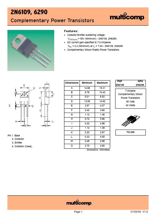
Features:•Collector-Emitter sustaining voltage-V CEO(sus)= 50V (Minimum) - 2N6109, 2N6290.•DC current gain specified to 7.0 Amperesh FE = 2.3 (Minimum) at I C = 7.0A - 2N6109, 2N6290.•Complementary Silicon Plastic Power Transistors.Dimensions : MillimetresPin 1. Base2. Collector3. Emitter4. Collector (Case).Thermal CharacteristicFigure 1 - Power DeratingElectrical Characteristics (T C = 25°C unless otherwise noted)There are two limitations on the power handling ability of a transistor:average junction temperature and second breakdown safe operating area curves indicate I reliable operation i.e., the transistor must not be subjected to greater dissipation than the curves indicate.The data of Figure - 6 curve is based on T depending on the power level. Second breakdown pulse limits are valid for duty cycles to 10% provided T thermal limitation will reduce the power that can be handled to values less than the limitations imposed by second breakdown.Figure 3 - Turn-Off TimeFigure 2 - Switching Time Test CircuitFigure 4 - DC Current Gain Figure 5 - Turn-On TimeD1 must be fast recovery type, example:MB05300 used above IB = 100mA MSD6100 used below IB = 100mAFigure 7 - Collector Saturation RegionFigure 9 - “ON” Voltage Figure 10 - Collector Cut-Off RegionFigure 8 - CapacitancesNotes:FRANCE –Farnell InOneTel No:++ 33 474 68 99 99Fax No:++33 474 68 99 90–Farnell InOne++ 45 44 53 66 66No:++ 45 44 53 66 02AUSTRIA –Farnell InOneTel No:++ 43 662 2180 680Fax No:++43 662 2180 670GERMANY –Farnell InOneTel No:++ 49 89 61 39 39 39Fax No:++49 89 613 59 01PORTUGAL –Farnell InOneTel No:++ 34 93 475 8804Fax No:++34 93 474 5288ESTONIA –Farnell InOneTel No:++ 358 9 560 7780Fax No:++358 9 345 5411NETHERLANDS –Farnell InOneTel No:++ 31 30 241 7373Fax No:++31 30 241 7333–Farnell InOne++ 44 8701 200 200No:++44 8701 200 201–++ 65 6788 0200No:++65 6788 0300HONG KONG –Farnell-Newark InOneTel No:++ 852 2268 9888Fax No:++852 2268 9899BELGIUM –Farnell InOneTel No:++ 32 3 475 2810Fax No:++32 3 227 3648BRAZIL – Farnell-Newark InOneTel No:++ 55 11 4066 9400Fax No:++55 11 4066 9410IRELAND –Farnell InOneTel No:++ 353 1 830 9277Fax No:++353 1 830 9016SPAIN –Farnell InOneTel No:++ 34 93 475 8805Fax No:++34 93 474 5107CHINA –Farnell-Newark InOneTel No:++86 10 6238 5152Fax No: ++86 10 6238 5022ITAL Y –Farnell InOneTel No:++ 39 02 93 995 200Fax No:++ 39 02 93 995 300SWEDEN –Farnell InOneTel No:++ 46 8 730 50 00Fax No:++46 8 83 52 62MALAYSIA –Farnell-Newark InOneTel No:++ 60 3 7873 8000Fax No:++60 3 7873 7000SWITZERLAND –Farnell InOneTel No:++ 41 1 204 64 64Fax No:++41 1 204 64 54DENMARK –Farnell InOneTel No:++ 45 44 53 66 44Fax No:++45 44 53 66 06–CPC–BuckHickman InOneNEW ZEALAND –Farnell InOneTel No:++ 64 9 357 0646Fax No:++64 9 357 0656 。
BSS89中文资料
BSS89
UNIT V V mA A W °C °C
THERMAL CHARACTERISTICS SYMBOL Rth j-a PARAMETER thermal resistance from junction to ambient CONDITIONS note 1 VALUE 125 UNIT K/W
元器件交易网
DISCRETE SEMICONDUCTORS
DATA SHEET
BSS89 N-channel enhancement mode vertical D-MOS transistor
Product specification Supersedes data of 1997 Jun 20 File under Discrete Semiconductors, SC13b 1998 Apr 24
Limiting values given are in accordance with the Absolute Maximum Rating System (IEC 134). Stress above one or more of the limiting values may cause permanent damage to the device. These are stress ratings only and operation of the device at these or at any other conditions above those given in the Characteristics sections of the specification is not implied. Exposure to limiting values for extended periods may affect device reliability. Application information Where application information is given, it is advisory and does not form part of the specification. LIFE SUPPORT APPLICATIONS These products are not designed for use in life support appliances, devices, or systems where malfunction of these products can reasonably be expected to result in personal injury. Philips customers using or selling these products for use in such applications do so at their own risk and agree to fully indemnify Philips for any damages resulting from such improper use or sale.
E36-3C90-E100中文资料(ferroxcube)中文数据手册「EasyDatasheet - 矽搜」
核心组功率条件下属性
B( MT)在
GRADE 3C90
H = 250 A /米 ; F = 25千赫 ; T = 100 °C
330
µe 61 97 152 191 243 382 1610
F = 25千赫 ; Bˆ = 200 mT; T = 100 °C
1.4
Dimensionsin mm.
图1 E36/21/12核心一半.
E36/21/12
VALUE 0.762 12160 96 126 121
31
UNIT mm 1 mm 3 mm mm 2 mm 2 g
handbook, halfpage handbook, halfpage
36 ±0.7 +1.2
24.5 0 10.2 0 0.5
+0.6
15.75
0 21.75
飞磁
E型磁芯及配件
E36/21/12
数据表状态定义
数据表 状态
初稿 规范
产品规格
产品 状态
发育
生产
定义
此数据表包含初稿数据.飞磁防护留在任何时间更改,恕不另行通知,以 提高设计和提供最好产品权利.
此数据表包含最终规格.飞磁防护留在任何时间更改,恕不另行通知,以提 高设计和提供最好产品权利.
免责声明
生命支持应用
L 测量,40
±20 N.
铁心损耗( W)在
F = 100千赫 ; Bˆ = 00 mT;
T = 100 °C
F = 100千赫 ; Bˆ = 200 mT;
T = 25 °C
1.5
F = 100千赫 ; Bˆ = 200 mT;
T = 100 °C
89s 系列 后缀
ATmega8-16MU MLF32 4.5V-5.5V 16MHz
×=A,表示TQFP封装。
×=W,表示裸芯片。
后缀中第三个参数×用于表示温度范围,它的意义如下:
×=C,表示商业产品,温度范围为0至+70℃。
×=I,表示工业产品,温度范围为-40至+85℃。
×=A,表示汽车用产品,温度范围为-40至+125℃。
后缀中的第二个参数×用于表示封装。它的意义如下:
×=D,Cerdip。
×=J,塑料J引线芯片载体。
×=L,无引线芯片载体。
×=P,表示塑料双列直插DIP封装。
×=S,表示SOIC封装。
×=Q,表示PQFP封装。
②、后缀的数字部分,表示支持的最高系统时钟。
例:ATmega8-16MU,“16”表示可支持最高为16MHZ的系统时钟。
③、后缀第一(第二)个字母,表示封装。“P”:DIP封装,“A”:TQFP封装,“M”:MLF封装。
例:ATmega8-16MU,“M”表示MLF封装。
④、后缀最后一个字母,表示应用级别。“C”:商业级,“I”:工业级(有铅)、“U”工业级(无铅)。
后缀由“××××”这4个参数组成。每个参数的表示和意义不同。在型号与后缀部分有“-”号隔开。
后缀中的第一个参数×用于表示速度,它的意义如下:
×=12,表示速度为12MHz,
×=16,表示速度为16MHz,
×=20,表示速度为20MHz,
×=24,表示速度为24MHz,
型号 封装 工作电压范围 支持最大速度 其他属性、性能
MAX629ESA中文资料
1
For free samples & the latest literature: , or phone 1-800-998-8800
元器件交易网
28V, Low-Power, High-Voltage, Boost or Inverting DC-DC Converter MAX629
Stresses beyond those listed under “Absolute Maximum Ratings” may cause permanent damage to the device. These are stress ratings only, and functional operation of the device at these or any other conditions beyond those indicated in the operational sections of the specifications is not implied. Exposure to absolute maximum rating conditions for extended periods may affect device reliability.
元器件交易网
19-1219; Rev 1; 6/97
ANUAL N KIT M IO T A U EVAL BLE AVAILA
28V, Low-Power, High-Voltage, Boost or Inverting DC-DC Converter
____________________________Features
___________________________________________________Typical Operating Circuit
S-80926中文资料
Table 1
Detection voltage range (V) 1.1V±2.0% 1.2V±2.0% 1.3V±2.0% 1.4V±2.0% 1.5V±2.0% 1.6V±2.0% 1.7V±2.0% 1.8V±2.0% 1.9V±2.0% 2.0V±2.0% 2.1V±2.0% 2.2V±2.0% 2.3V±2.0% 2.4V±2.0% 2.5V±2.0% 2.6V±2.0% 2.7V±2.0% 2.8V±2.0% 2.9V±2.0% 3.0V±2.0% 3.1V±2.0% 3.2V±2.0% 3.3V±2.0% 3.4V±2.0% 3.5V±2.0% 3.6V±2.0% 3.7V±2.0% 3.8V±2.0% 3.9V±2.0% 4.0V±2.0% 4.1V±2.0% 4.2V±2.0% 4.3V±2.0% 4.4V±2.0% 4.5V±2.0% 4.6V±2.0% 4.7V±2.0% 4.8V±2.0% 4.9V±2.0% 5.0V±2.0% 5.1V±2.0% 5.2V±2.0% 5.3V±2.0% 5.4V±2.0% 5.5V±2.0% 5.6V±2.0% 5.7V±2.0% 5.8V±2.0% 5.9V±2.0% 6.0V±2.0% Hysteresis width VHYS typ.(V) 0.055 0.060 0.065 0.070 0.075 0.080 0.085 0.090 0.095 0.100 0.105 0.110 0.115 0.120 0.125 0.130 0.135 0.140 0.145 0.150 0.155 0.160 0.165 0.170 0.175 0.180 0.185 0.190 0.195 0.200 0.205 0.210 0.215 0.220 0.225 0.230 0.235 0.240 0.245 0.250 0.255 0.260 0.265 0.270 0.275 0.280 0.285 0.290 0.295 0.300 Nch Open Drain(Low) S-80911ANMP-D71-T2 S-80912ANMP-D72-T2 S-80913ANMP-DDA-T2 S-80914ANMP-DDB-T2 S-80915ANMP-DDC-T2 S-80916ANMP-DDD-T2 S-80917ANMP-DDE-T2 S-80918ANMP-DDF-T2 S-80919ANMP-DDG-T2 S-80920ANMP-DDH-T2 S-80921ANMP-DDJ-T2 S-80922ANMP-DDK-T2 S-80923ANMP-DDL-T2 S-80924ANMP-DDM-T2 S-80925ANMP-DDN-T2 S-80926ANMP-DDP-T2 S-80927ANMP-DDQ-T2 S-80928ANMP-DDR-T2 S-80929ANMP-DDS-T2 S-80930ANMP-DDT-T2 S-80931ANMP-DDV-T2 S-80932ANMP-DDW-T2 S-80933ANMP-DDX-T2 S-80934ANMP-DDY-T2 S-80935ANMP-DDZ-T2 S-80936ANMP-DD0-T2 S-80937ANMP-DD1-T2 S-80938ANMP-DD2-T2 S-80939ANMP-DD3-T2 S-80940ANMP-DD4-T2 S-80941ANMP-DD5-T2 S-80942ANMP-DD6-T2 S-80943ANMP-DD7-T2 S-80944ANMP-DD8-T2 S-80945ANMP-DD9-T2 S-80946ANMP-DJA-T2 S-80947ANMP-DJB-T2 S-80948ANMP-DJC-T2 S-80949ANMP-DJD-T2 S-80950ANMP-DJE-T2 S-80951ANMP-DJF-T2 S-80952ANMP-DJG-T2 S-80953ANMP-DJH-T2 S-80954ANMP-DJJ-T2 S-80955ANMP-DJK-T2 S-80956ANMP-DJL-T2 S-80957ANMP-DJM-T2 S-80958ANMP-DJN-T2 S-80959ANMP-DJP-T2 S-80960ANMP-DJQ-T2 CMOS Output(Low) S-80911ALMP-D51-T2 S-80912ALMP-D52-T2 S-80913ALMP-DAA-T2 S-80914ALMP-DAB-T2 S-80915ALMP-DAC-T2 S-80916ALMP-DAD-T2 S-80917ALMP-DAE-T2 S-80918ALMP-DAF-T2 S-80919ALMP-DAG-T2 S-80920ALMP-DAH-T2 S-80921ALMP-DAJ-T2 S-80922ALMP-DAK-T2 S-80923ALMP-DAL-T2 S-80924ALMP-DAM-T2 S-80925ALMP-DAN-T2 S-80926ALMP-DAP-T2 S-80927ALMP-DAQ-T2 S-80928ALMP-DAR-T2 S-80929ALMP-DAS-T2 S-80930ALMP-DAT-T2 S-80931ALMP-DAV-T2 S-80932ALMP-DAW-T2 S-80933ALMP-DAX-T2 S-80934ALMP-DAY-T2 S-80935ALMP-DAZ-T2 S-80936ALMP-DA0-T2 S-80937ALMP-DA1-T2 S-80938ALMP-DA2-T2 S-80939ALMP-DA3-T2 S-80940ALMP-DA4-T2 S-80941ALMP-DA5-T2 S-80942ALMP-DA6-T2 S-80943ALMP-DA7-T2 S-80944ALMP-DA8-T2 S-80945ALMP-DA9-T2 S-80946ALMP-DEA-T2 S-80947ALMP-DEB-T2 S-80948ALMP-DEC-T2 S-80949ALMP-DED-T2 S-80950ALMP-DEE-T2 S-80951ALMP-DEF-T2 S-80952ALMP-DEG-T2 S-80953ALMP-DEH-T2 S-80954ALMP-DEJ-T2 S-80955ALMP-DEK-T2 S-80956ALMP-DEL-T2 S-80957ALMP-DEM-T2 S-80958ALMP-DEN-T2 S-80959ALMP-DEP-T2 S-80960ALMP-DEQ-T2
6639S-1-103;6639S-1-102;6639S-1-104;6639S-1-202;6639S-1-203;中文规格书,Datasheet资料
22.23 (.875) DIA.
3.18 (.125)
6639
11.25 .38 (.443 .015)
1.57 (.062)
Байду номын сангаас
22.23 (.875) DIA.
.51 (.020) REF
19.81 (.780) DIA.
12.70 .79 (.500 .031)
10.317+.000/-.051 (.4062+.000/-.002)
DIA.
6.342+.000/-.008
(.2497+.0000/-.0003) DIA. SHAFT .25
45 5 (.010) CHAMFER 1.19 1.60
SLOT (.047) X (.063)
Mechanical Characteristics1
Mechanical Angle ..........................................................Continuous, Stops (340 ° +8 °, -0 °) available Torque (Starting & Running)2 ...................................................................0.40 N-cm (0.5 oz.-in.) max.
Sea Level......................................... 750 VAC minimum .....................750 VAC minimum Power Rating (Voltage Limited By Power Dissipation or 300 VAC, Whichever is Less)
Mobilgear 629 (中文)
610865-00 MOBILGEAR 629产 品 安 全 技 术 说 明 书第一部分 产品和企业标识产品名称:MOBILGEAR 629 供应商名称、地址及电话:埃克森美孚(中国)投资有限公司 上海市天钥桥路30号 美罗大厦 200030 86-21-5464 4588紧急联络电话:86-21-5464 4588传真电话:86-21-6427 0570第二部分 成分/组成信息化学名称和别名:石油碳氢化合物和添加剂。
全球报告的MSDS成分:无。
接触限值(若适用)见第8部分。
第三部分 危险性概述在正常使用条件下,依照法规认为本品无害(参见15部分)。
应急综述: 微浊琥珀色液体。
美国运输部(DOT)紧急情况响应指导书(ERG)编号: 不适用。
潜在健康影响:在正常的预期使用条件下,本品对健康没有危险。
过度接触会引起眼睛、 皮肤或呼吸刺激。
进一步的健康影响/毒理学资料参见第11部分。
第四部分 急救措施眼睛接触:用清水彻底冲洗。
若出现刺激,就医。
皮肤接触:用肥皂和清水冲洗污染皮肤。
脱掉被油浸湿的衣服并洗干净,清洗污染皮肤。
(参见第16部分-注射伤害)。
吸 入:一般不会有问题。
但是,如果由于过多接触蒸气或雾出现呼吸刺激、眩晕、恶心 或神志不清,立即就医。
如果呼吸停止,用机械装置或口对口的方式进行人工呼吸。
食 入:一般不会有问题。
若感觉不适,就医。
禁止催吐。
第五部分 消防措施灭 火 剂:二氧化碳、泡沫、干粉和雾状水。
特殊灭火程序:用水或泡沫灭火可导致喷沫。
用水冷却暴露在火场中的容器。
可使用雾状 水从暴露区域冲走泄漏物。
防止泄漏物从受控的火场流出或被稀释后排入河流、下水 道或饮用水供应系统。
防护器具:在封闭的区域灭火,消防员必须佩戴自给式呼吸器。
异常燃爆危险:无。
燃烧产物:在不完全燃烧的情况下,有浓烟、一氧化碳、硫的氧化物、醛和其它分解产物 。
闪点℃(℉):204 (399) (ASTM D-92)。
HB6296应用指南 (1)
HB6296应用指南
一:电流检测电阻设法靠近hb6296,检测电阻上电压信号很弱,为减少干扰,必须靠近hb6296,应用图上对应的R17.
二:Regn上电容必须靠近hb6296,越近越好。
三:这款ic是经典的降压电路,电感计算公式可以参考。
四:电感计算公式:L=(Vin-Vbat)*Ton/(Imax/D)。
其中D是占空比,Ton=T*D。
L=(Vin-Vbat)*T。
T是开关周期,Vbat取3.7*n 节。
HB6296的开关频率是变的,电压高是350K,(T=2.8us)。
电压低是1.8us。
对4节锂电,输入电压25V,输出电流5A。
则L=(25-14.8)*1.8us/5A=3.6uH。
五:散热。
对于低压(小于35V),我测试的结果hb6296不需要加散热片,P=(35V-5.4)*12ma=360mw,HB6296本身带散热片,外面可以不加。
如果驱动2个上管mosfet,Icc会上升到20ma,这时P=(35-5.4)*20ma=600mw,应该考虑加散热片。
Mosfet的散热也要特别讲究。
主要要考虑上管(pwm管)。
六:mosfet选择最好要用Ciss小的,tr,tf比较短的,mosfet。
这样mosfet发热少,hb6296发热也少。
但是也不能太少,太少电感波形太陡,emc和emi过不去,也干扰hb6296。
七:为了emc和emi的考虑,主电流回路要越短越好,交流回路也要越短越好,特别是lx这个net上,交流通路可以用4.7uf 的瓷片电容放置相关的地方,比较有效的减少交流通路的长度。
2N6796中文资料

Min.
100
Typ.
Max. Unit
V 250 1000 100 –100 µA
VDS=Rated VDSS
nA
ON CHARACTERISTICS
Gate Thresshold Voltage Static Drain–Source On–Resistance Drain–Source On–Voltage Forward Transconductance 2.0 4.0 0.18 0.35 1.56 3.0 350 150 50 9.0. 900 500 150 30 VDD = 30V ID = 5.0A 75 40 45 0.75 1.5
Prelim. 11/98
Underside View PIN 1 – Source PIN 2 – Gate PIN 3 – Drain Case
ABSOLUTE MAXIMUM RATINGS (Tcase = 25°C unless otherwise stated)
Drain–Source Voltage VDGR Drain–Gate Voltage (RGS = 1.0mΩ) VGS Gate–Source Voltage ID Drain Current Continuous IDM Drain Current Pulsed PD Total Device Dissipation @ TC = 25°C Derate above 25°C TJ , TSTG Operating and Storage Junction Temperature Range THERMAL CHARACTERISTICS RθJC Thermal Resistance Junction to Case RθJC Thermal Resistance Junction to Ambient TL Maximum Lead Temperature 1.5mm from Case for 10 s VDSS 100V 100V ±20V 8.0A 32A 25W 0.2W/ °CW –55 to +150°C 5.0°CW 175°CW 300°C
爱尔顿 Moeller 系列快速链接速控器 198996 数据表 说明书
Eaton 198996Eaton Moeller® series Rapid Link - Speed controllers, 5.6 A, 2.2 kW, Sensor input 4, Actuator output 2, PROFINET, HAN Q4/2General specificationsEaton Moeller® series Rapid Link Speed controller1989964015081970544157 mm 270 mm 220 mm 3.44 kg IEC/EN 61800-5-1 UL 61800-5-1 RoHS UL approval CEProduct NameCatalog NumberEANProduct Length/Depth Product Height Product Width Product Weight Certifications Catalog Notes 3 fixed speeds and 1 potentiometer speedcan be switched over from U/f to (vector) speed control Connection of supply voltage via adapter cable on round or flexible busbar junction Diagnostics and reset on the device and via PROFINET integrated PTCParameterization: drivesConnectParameterization: KeypadParameterization: FieldbusParameterization: drivesConnect mobile (App)PTC thermistor monitoringControl unitKey switch position AUTO2 Actuator outputsInternal DC linkIGBT inverterKey switch position HANDThermo-click with safe isolationPC connectionKey switch position OFF/RESETTwo sensor inputs through M12 sockets (max. 150 mA) for quick stop and interlocked manual operationSelector switch (Positions: REV - OFF - FWD)3 fixed speeds1 potentiometer speed NEMA 12IP651st and 2nd environments (according to EN 61800-3)IIISpeed controllerPROFINET IOC1: for conducted emissions onlyC2, C3: depending on the motor cable length, the connected load, and ambient conditions. External radio interference suppression filters (optional) may be necessary.2000 VAC voltagePhase-earthed AC supply systems are not permitted. Center-point earthed star network (TN-S network)Vertical15 g, Mechanical, According to IEC/EN 60068-2-27, 11 ms, Half-sinusoidal shock 11 ms, 1000 shocks per shaftResistance: According to IEC/EN 60068-2-6Resistance: 57 Hz, Amplitude transition frequency on accelerationResistance: 6 Hz, Amplitude 0.15 mmResistance: 10 - 150 Hz, Oscillation frequency Max. 2000 mAbove 1000 m with 1 % performance reduction per 100 m -10 °C40 °C-40 °C70 °CFeatures Fitted with:Functions Degree of protectionElectromagnetic compatibility Overvoltage categoryProduct categoryProtocolRadio interference classRated impulse withstand voltage (Uimp) System configuration typeMounting position Shock resistance Vibration AltitudeAmbient operating temperature - min Ambient operating temperature - max Ambient storage temperature - min Ambient storage temperature - max Climatic proofing< 95 %, no condensationIn accordance with IEC/EN 50178Current limitation0.5 - 5.6 A, motor, main circuitAdjustable, motor, main circuitDelay time< 10 ms, Off-delay< 10 ms, On-delayEfficiency98 % (η)Input current ILN at 150% overload5.3 ALeakage current at ground IPE - max3.5 mAMains current distortion120 %Mains switch-on frequencyMaximum of one time every 60 secondsMains voltage - min380 VMains voltage - max480 VMains voltage tolerance380 - 480 V (-10 %/+10 %, at 50/60 Hz)Operating modeSensorless vector control (SLV)U/f controlSynchronous reluctance motorsPM and LSPM motorsBLDC motorsOutput frequency - min0 HzOutput frequency - max500 HzOverload currentFor 60 s every 600 sAt 40 °COverload current IL at 150% overload8.4 A45 Hz66 Hz5.6 A at 150% overload (at an operating frequency of 8 kHz and an ambient air temperature of +40 °C)2.2 kW480 V AC, 3-phase400 V AC, 3-phase0.1 Hz (Frequency resolution, setpoint value)200 %, IH, max. starting current (High Overload), For 2 seconds every 20 seconds, Power section50/60 Hz8 kHz, 4 - 32 kHz adjustable, fPWM, Power section, Main circuitAC voltagePhase-earthed AC supply systems are not permitted.Center-point earthed star network (TN-S network)3 HP≤ 0.6 A (max. 6 A for 120 ms), Actuator for external motor brakeAdjustable to 100 % (I/Ie), DC - Main circuit10 kAType 1 coordination via the power bus' feeder unit, Main circuit 24 V DC (-15 %/+20 %, external via AS-Interface® plug)PROFINET, optionalPlug type: HAN Q4/2Max. total power consumption from AS-Interface® power supply unit (30 V): 250 mASpecification: S-7.4 (AS-Interface®)Number of slave addresses: 31 (AS-Interface®)Rated frequency - minRated frequency - maxRated operational current (Ie)Rated operational power at 380/400 V, 50 Hz, 3-phase Rated operational voltageResolutionStarting current - maxSupply frequencySwitching frequencySystem configuration type Assigned motor power at 460/480 V, 60 Hz, 3-phase Braking currentBraking torqueRated conditional short-circuit current (Iq)Short-circuit protection (external output circuits) Rated control voltage (Uc)Communication interfaceConnectionInterfacesCable length10.2.2 Corrosion resistanceC3 ≤ 25 m, maximum motor cable length C1 ≤ 1 m, maximum motor cable length C2 ≤ 5 m, maximum motor cable length Meets the product standard's requirements.Meets the product standard's requirements.Meets the product standard's requirements.Meets the product standard's requirements.Meets the product standard's requirements.Does not apply, since the entire switchgear needs to be evaluated.Does not apply, since the entire switchgear needs to be evaluated.Meets the product standard's requirements.Does not apply, since the entire switchgear needs to be evaluated.Meets the product standard's requirements.Does not apply, since the entire switchgear needs to be evaluated.Does not apply, since the entire switchgear needs to be evaluated.Is the panel builder's responsibility.Is the panel builder's responsibility.Is the panel builder's responsibility.Is the panel builder's responsibility.10.2.3.1 Verification of thermal stability of enclosures10.2.3.2 Verification of resistance of insulating materials to normal heat10.2.3.3 Resist. of insul. mat. to abnormal heat/fire by internal elect. effects10.2.4 Resistance to ultra-violet (UV) radiation10.2.5 Lifting10.2.6 Mechanical impact10.2.7 Inscriptions10.3 Degree of protection of assemblies10.4 Clearances and creepage distances10.5 Protection against electric shock10.6 Incorporation of switching devices and components10.7 Internal electrical circuits and connections10.8 Connections for external conductors10.9.2 Power-frequency electric strength10.9.3 Impulse withstand voltage10.9.4 Testing of enclosures made of insulating materialIs the panel builder's responsibility.The panel builder is responsible for the temperature risecalculation. Eaton will provide heat dissipation data for the devices.Is the panel builder's responsibility. The specifications for the switchgear must be observed.Is the panel builder's responsibility. The specifications for the switchgear must be observed.The device meets the requirements, provided the information in the instruction leaflet (IL) is observed.Generation change RAMO4 to RAMO5Generation change from RA-SP to RASP 4.0Generation change from RA-MO to RAMO 4.0Generation Change RASP4 to RASP5Electromagnetic compatibility (EMC)Generation Change RA-SP to RASP5Connecting drives to generator suppliesConfiguration to Rockwell PLC for Rapid LinkRapid Link 5 - brochureDA-SW-drivesConnect USB Driver DX-COM-PCKITDA-SW-USB Driver PC Cable DX-CBL-PC-1M5DA-SW-drivesConnectDA-SW-drivesConnect - installation helpDA-SW-Driver DX-CBL-PC-3M0DA-SW-drivesConnect - InstallationshilfeDA-SW-USB Driver DX-COM-STICK3-KITMaterial handling applications - airports, warehouses and intra-logisticsProduct Range Catalog Drives EngineeringProduct Range Catalog Drives Engineering-ENDA-DC-00003964.pdfDA-DC-00004184.pdfDA-DC-00004514.pdfDA-DC-00004508.pdfeaton-bus-adapter-rapidlink-speed-controller-dimensions-002.eps eaton-bus-adapter-rapidlink-speed-controller-dimensions-003.eps eaton-bus-adapter-rapidlink-speed-controller-dimensions.epseaton-bus-adapter-rapidlink-speed-controller-dimensions-004.eps ETN.RASP5-5420PNT-4120000S1.edzIL034093ZU10.10 Temperature rise10.11 Short-circuit rating10.12 Electromagnetic compatibility10.13 Mechanical functionApplication notesBrochuresCataloguesCertification reportsDrawingseCAD modelInstallation instructionsEaton Corporation plc Eaton House30 Pembroke Road Dublin 4, Ireland © 2023 Eaton. All rights reserved. Eaton is a registered trademark.All other trademarks areproperty of their respectiveowners./socialmediaRapid Link 5MN040003_EN MN034004EN MZ040046_EN DA-MN-MZ040045EN rasp5_v35.stp ramo5_v35.dwgInstallation videos Manuals and user guides mCAD model。
单片机芯片资料
深圳好记芯电子有限公司 TEL:0755-86100886 FAX:0755-86100961
第 一 章 SST 系列单片机原理
1.1 功能框图
5
深圳好记芯电子有限公司 TEL:0755-86100886 FAX:0755-86100961
保护你的知识权益.
型号
SST89 E / V 516RD2 SST89 E / V 58RD2 SST89 E / V 54RD2 SST89 E / V 52RD2 SST89 E / V 54RC SST89 E / V 52RC
SST89 系列单片机选型一览表
最高时钟
Flash
串口 PCA 中 优 DPTR 降低 掉 看 双 P S
产品简介:
SST89E516RD、SST89V516RD、SST89E58RD 和 SST89V58RD 都是 8 位 FLASH FLEX51 系列单片机。FLASH FLEX51 是在高级 FLASH CMOS 半导体工艺下设计和生产出 的单片机产品之一。器件都有相同的功能强大的指令系统,并且和 8xC5x 器件兼容。
(扇区大小为 128 字节) —SST89E58RD/SST89V58RD:32K*8 的基本存储块和 8K*8 的二级存储块(扇 区大小为 128 字节),( 二级存储块可用于存放掉电后要保存的数据,放在内部 具有极强的抗干扰性) —独立的块加密 —IAP 下的并行操作 —块地址重映射 · 最大片外程序/数据地址空间为 64K*8(当然也可以通过 I/O 口进行块切换,实 现超 64K 扩展) · 三个高电流驱动引脚(每个 16 mA,可直接驱动 LED) · 三个 16 位定时器/计数器 · 全双工增强型 UART
TTL 负载。 P0 浮空,锁存器为“1”,可作为高阻抗输入。 在访问外部存储器时,
2296786中文资料

Round cable set, for connection to Allen Bradley SLC 500, OB 32 and IB 32, with one 40-position socket strip and four 14-position socket strips, for splitting 32 channels into 4x8 channels, for OB 32, no. of positions 40/4x14, cable length 0.5 m
http://eshop.phoenixcontact.de/phoenix/treeViewClick.do?UID=2296786
Address
PHOENIX CONTACT GmbH & Co. KG Flachsmarktstr. 8 32825 Blomberg,Germany Phone +49 5235 3 00 Fax +49 5235 3 41200 http://www.phoenixcontact.de
Max. conductor resistance Ambient temperature (operation) Ambient temperature (storage/transport) Number of positions, control side Number of connectors, control side Number of positions, module side Number of connectors, modul side Fixed cable length Single wire, cross section AWG Conductor construction: Number of litz wires: Single wire, material External diameter Cable, preassembly Shielding Certificates / Approvals
用于垂直磁记录介质的基板和用该基板的垂直磁记录介质[发明专利]
![用于垂直磁记录介质的基板和用该基板的垂直磁记录介质[发明专利]](https://img.taocdn.com/s3/m/65a6af34240c844768eaeeae.png)
专利名称:用于垂直磁记录介质的基板和用该基板的垂直磁记录介质
专利类型:发明专利
发明人:上住洋之,中岛典彦,川田辰实,樋口和人
申请号:CN200510056923.X
申请日:20050323
公开号:CN1677509A
公开日:
20051005
专利内容由知识产权出版社提供
摘要:本发明的一个目的是提供一种用于垂直磁记录介质的基板,该基板具有足够的生产能力,充当垂直磁记录介质的软磁性衬里层并确保表面硬度。
本发明还提供了使用这种基板的垂直磁记录介质。
该基板包括一个由铝合金构成的非磁性基体1,一层在非磁性基体上形成的而且由至少含镍的材料构成的粘附层2,和一层通过无电镀膜法在粘附层2上形成的软磁性底层3,该软磁性底层3含有
3at%至20at%的磷和在除磷外的钴和镍的原子数中的比例(Co/(Co+Ni))为至少25at%的钴;粘附层的厚度为至少0.1μm。
软磁性底层的厚度为至少0.2μm,粘附层和软磁性底层的厚度总和为至少
3μm。
申请人:富士电机电子设备技术株式会社
地址:日本东京
国籍:JP
代理机构:北京纪凯知识产权代理有限公司
代理人:龙淳
更多信息请下载全文后查看。
FDU6296资料
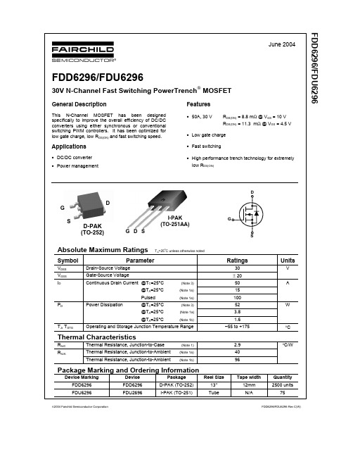
Parameter
Drain-Source Voltage Gate-Source Voltage Continuous Drain Current @TC=25°C @TA=25°C Pulsed
(Note 3) (Note 1a) (Note 1a) (Note 3) (Note 1a) (Note 1b)
(Note 2)
Test Conditions
Single Pulse, VDD = 15 V, ID=15A
Min Typ Max Units
165 15 mJ A
Drain-Source Avalanche Ratings (Note 2)
Off Characteristics
BVDSS ∆BVDSS ∆TJ IDSS IGSS VGS = 0 V, ID = 250 µA 30 29 1 ± 100 1 1.7 –0.5 7.5 9.0 9.3 58 1440 400 140 VGS = 15 mV,
90 VDS = 10V ID , D R A I N C U R R E N T (A)
IS , R E V E R S E D R A I N C U R R E N T ( A ) 1000 100 10 1
a) RθJA = 40°C/W when mounted on a 1in2 pad of 2 oz copper
b) RθJA = 96°C/W when mounted on a minimum pad.
Scale 1 : 1 on letter size paper 2. Pulse Test: Pulse Width < 300µs, Duty Cycle < 2.0% 3. Maximum current is calculated as: current limitation is 21A
- 1、下载文档前请自行甄别文档内容的完整性,平台不提供额外的编辑、内容补充、找答案等附加服务。
- 2、"仅部分预览"的文档,不可在线预览部分如存在完整性等问题,可反馈申请退款(可完整预览的文档不适用该条件!)。
- 3、如文档侵犯您的权益,请联系客服反馈,我们会尽快为您处理(人工客服工作时间:9:00-18:30)。
SIPMOS ® Small-Signal Transistor• N channel• Enhancement mode• Logic Level• V GS(th) = 0.8...2.0VPin 1Pin 2Pin 3G D S Type V DS I D R DS(on)Package MarkingBSS 89240 V0.3 A 6 ΩTO-92SS89Type Ordering Code Tape and Reel InformationBSS 89Q62702-S519E6288BSS 89Q62702-S619E6296BSS 89Q62702-S385E6325Maximum RatingsParameter Symbol Values Unit Drain source voltage V DS 240VDrain-gate voltage R GS = 20 kΩVDGR240Gate source voltage V GS± 20 ESD Sensitivity (HBM) as per MIL-STD 883Class 1Continuous drain current T A = 25 ˚C I D0.3ADC drain current, pulsed T A = 25 ˚C I Dpuls1.2Power dissipation T A = 25 ˚C P tot1WBSS 89Maximum RatingsParameter Symbol Values Unit Chip or operating temperature T j -55 ... + 150˚C Storage temperature T stg -55 ... + 150 Thermal resistance, chip to ambient air 1)R thJA≤ 125K/W DIN humidity category, DIN 40 040 EIEC climatic category, DIN IEC 68-1 55 / 150 / 56Electrical Characteristics, at T j = 25˚C, unless otherwise specifiedParameter Symbol Values Unitmin.typ.max.Static CharacteristicsDrain- source breakdown voltage V GS = 0 V, I D = 0.25 mA, T j = 25 ˚C V(BR)DSS240--VGate threshold voltage V GS=V DS, I D = 1 mA V GS(th)0.8 1.5 2Zero gate voltage drain currentV DS = 240 V, V GS = 0 V, T j = 25 ˚C V DS = 240 V, V GS = 0 V, T j = 125 ˚C V DS = 60 V, V GS = 0 V, T j = 25 ˚C I DSS----100.10.21001µAGate-source leakage current V GS = 20 V, V DS = 0 V I GSS- 10 100nADrain-Source on-state resistance V GS = 10 V, I D = 0.3 AV GS = 4.5 V, I D = 0.3 A R DS(on)--5.34.5106ΩElectrical Characteristics, at T j = 25˚C, unless otherwise specifiedParameter Symbol Values Unitmin.typ.max.Dynamic CharacteristicsTransconductanceV DS≥ 2 *I D * R DS(on)max, I D = 0.3 A g fs0.14 0.33-SInput capacitanceV GS = 0 V, V DS = 25 V, f = 1 MHz C iss- 115 155pFOutput capacitanceV GS = 0 V, V DS = 25 V, f = 1 MHz C oss- 15 25Reverse transfer capacitanceV GS = 0 V, V DS = 25 V, f = 1 MHz C rss-812Turn-on delay timeV DD = 30 V, V GS = 10 V, I D = 0.28 A R G = 50 Ωt d(on)-58nsRise timeV DD = 30 V, V GS = 10 V, I D = 0.28 A R G = 50 Ωt r- 10 15Turn-off delay timeV DD = 30 V, V GS = 10 V, I D = 0.28 A R G = 50 Ωt d(off)- 30 40Fall timeV DD = 30 V, V GS = 10 V, I D = 0.28 A R G = 50 Ωt f- 20 27Electrical Characteristics, at T j = 25˚C, unless otherwise specifiedParameter Symbol Values Unitmin.typ.max.Reverse DiodeInverse diode continuous forward current T A = 25 ˚C I S-- 0.3AInverse diode direct current,pulsed T A = 25 ˚C I SM-- 1.2Inverse diode forward voltage V GS = 0 V, I F = 0.6 A V SD- 0.9 1.4VPower dissipation P tot = ƒ(T A )20406080100120˚C160T A 0.0 0.1 0.20.3 0.4 0.50.6 0.7 0.80.9 1.0W1.2 P totDrain current I D = ƒ(T A )parameter: V GS ≥ 10 V20406080100120˚C160T A0.000.040.08 0.120.160.200.24A0.32I DSafe operating area I D =f(V DS )parameter : D = 0.01, T C =25˚CDrain-source breakdown voltage V (BR)DSS = ƒ(T j )-60-202060100˚C 160T j215 220225 230 235 240 245 250 255 260 265 270275V 285 V (BR)DSSTyp. output characteristics I D = ƒ(V DS )parameter: t p = 80 µs2468V11VDS 0.000.050.10 0.15 0.20 0.25 0.30 0.35 0.40 0.45 0.50 0.55 0.60A 0.70 I DV GS [V] a a 2.0bb 2.5c c 3.0dd 3.5ee 4.0ff 4.5gg5.0h h6.0i i7.0j j8.0k k9.0l P tot = 1Wl10.0Typ. drain-source on-resistance R DS (on) = ƒ(I D )parameter: t p = 80 µs, T j = 25 ˚C0.000.100.200.300.40A 0.60I D2 46 8 10 12 14 16Ω19R DS (on)2.02.5V GS [V] =a a3.0b b3.5cc 4.0d d 4.5e e5.0f f6.0g g 7.0h h 8.0i i 9.0jj 10.0Typ. transfer characteristics I D = f (V GS )parameter: t p = 80 µs V DS ≥ 2 x I D x R DS(on)max12345678V10V GS0.0 0.20.40.60.8A1.2I DTyp. forward transconductance g fs = f (I D )parameter: t p = 80 µs,V DS ≥2 x I D x R DS(on)max0.000.100.200.300.40A0.55I D0.000.050.10 0.150.20 0.250.300.35 0.400.45 S0.55 g fsDrain-source on-resistance R DS (on) = ƒ(T j )parameter: I D = 0.3 A, V GS = 10 V-60-202060100˚C160T j0 1 2 3 4 5 6 7 8 9 10 11 1213Ω15R DS (on)typ98%Gate threshold voltage V GS (th) = ƒ(T j )parameter:V GS = V DS , I D = 1 mA0.0 0.4 0.8 1.21.62.0 2.42.83.2 3.64.0V 4.6 V GS(th)-60-202060100˚C160T j2%typ98%Typ. capacitancesC = f (V DS )parameter:V GS =0V, f = 1 MHz51015202530V40V DS10 110 210 310 pFCC rssC oss C issForward characteristics of reverse diode I F = ƒ(V SD )parameter: T j , t p = 80 µs-210 -110 010 110 AI F0.00.40.8 1.2 1.6 2.0 2.4V 3.0V SDT j = 25 ˚C typ T j = 25 ˚C (98%)T j = 150 ˚C typ T j = 150 ˚C (98%)。