IC datasheet pdf-EL5462 pdf datasheet (500MHz Low Power Current Feedback Amplifier)
IC datasheet pdf-OPA604,pdf(FET-Input, Low Distortion Operational Amplifier)
fA/√Hz
V dB
Ω || pF Ω || pF
dB
MHz V/µs µs µs
%
V mA mA Ω
V V mA
°C °C °C/W
OPA604
3
SBOS019A
THD + N (%)
Current Noise (fA/ Hz)
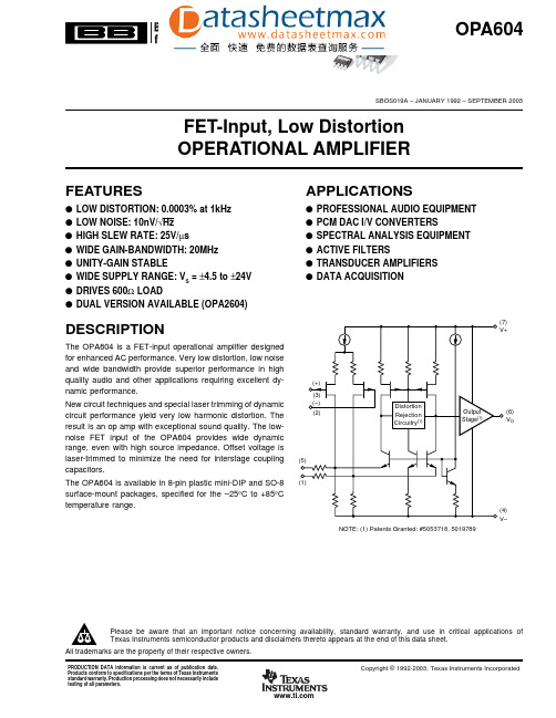
TYPICAL CHARACTERISTICS
Copyright © 1992-2003, Texas Instruments Incorporated
ABSOLUTE MAXIMUM RATINGS
Power Supply Voltage ....................................................................... ±25V Input Voltage ............................................................... (V–)–1V to (V+)+1V Output Short Circuit to Ground ................................................ Continuous Operating Temperature .................................................. –40°C to +100°C Storage Temperature ...................................................... –40°C to +125°C Junction Temperature .................................................................... +150°C Lead Temperature (soldering, 10s) AP .......................................... +300°C Lead Temperature (soldering, 3s) AU ............................................ +260°C
IC datasheet pdf-LT3652HV PDF DATASHEET
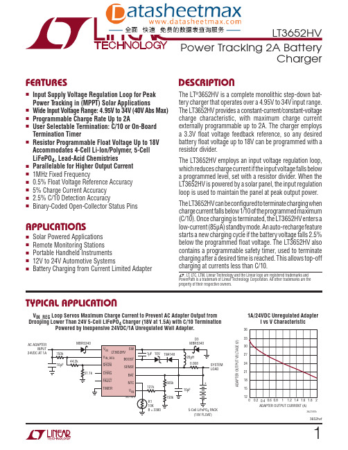
13652hvfT YPICAL APPLICATIOND ESCRIPTION ChargerThe LT ®3652HV is a complete monolithic step-down bat-tery charger that operates over a 4.95V to 34V input range. The LT3652HV provides a constant-current/constant-voltage charge characteristic, with maximum charge current externally programmable up to 2A. The charger employs a 3.3V fl oat voltage feedback reference, so any desired battery fl oat voltage up to 18V can be programmed with a resistor divider.The LT3652HV employs an input voltage regulation loop, which reduces charge current if the input voltage falls below a programmed level, set with a resistor divider. When the LT3652HV is powered by a solar panel, the input regulation loop is used to maintain the panel at peak output power.The L T3652HV c an b e c onfi gured t o t erminate c harging w hen charge c urrent f alls b elow 1/10 o f t he p rogrammed m aximum (C/10). Once charging is terminated, the LT3652HV enters a low-current (85μA) standby mode. An auto-recharge feature starts a new charging cycle if the battery voltage falls 2.5% below the programmed fl oat voltage. The LT3652HV also contains a programmable safety timer, used to terminate charging after a desired time is reached. This allows top-off charging at currents less than C/10.F EATURESA PPLICATIONS nInput Supply Voltage Regulation Loop for Peak Power T racking in (MPPT) Solar Applicationsn Wide Input Voltage Range: 4.95V to 34V (40V Abs Max)n Programmable Charge Rate Up to 2An User Selectable Termination: C/10 or On-Board Termination Timern Resistor Programmable Float Voltage Up to 18V Accommodates 4-Cell Li-Ion/Polymer , 5-Cell LiFePO 4, Lead-Acid Chemistriesn Parallelable for Higher Output Current n 1MHz Fixed Frequencyn 0.5% Float Voltage Reference Accuracy n 5% Charge Current Accuracy n 2.5% C/10 Detection Accuracyn Binary-Coded Open-Collector Status PinsnSolar Powered Applications n Remote Monitoring Stations n Portable Handheld Instruments n 12V to 24V Automotive SystemsnBattery Charging from Current Limited AdapterL , L T , L TC, L TM, Linear Technology and the Linear logo are registered trademarks and PowerPath is a trademark of Linear Technology Corporation. All other trademarks are the property of their respective owners.V IN_REG Loop Servos Maximum Charge Current to Prevent AC Adapter Output from Drooping Lower Than 24V 5-Cell LiFePO 4 Charger (18V at 1.5A) with C/10 TerminationPowered by Inexpensive 24VDC/1A Unregulated Wall Adapter.SYSTEM LOADD3ADAPTER OUTPUT CURRENT (A)00.2A D A P T E R O U T P U T V O L T A G E (V )12151833302724210.61 1.23652 TA01b360.40.8 1.61.421.81A/24VDC Unregulated AdapterI vs V CharacteristicLT3652HV23652hvfP IN CONFIGURATIONA BSOLUTE MAXIMUM RATINGS Voltages:V IN ........................................................................40V V IN_REG , SHDN , CHRG , FAUL T ............V IN + 0.5V , 40V SW ........................................................................40V SW-V IN .................................................................4.5V BOOST ...................................................SW+10V , 50V BAT , SENSE .. (20V)(Note 1)ORDER INFORMATIONLEAD FREE FINISH TAPE AND REEL PART MARKING*PACKAGE DESCRIPTION TEMPERATURE RANGE LT3652HVEDD#PBF LT3652HVEDD#TRPBF LFRG 12-Lead Plastic DFN 3mm × 3mm –40°C to 125°C LT3652HVIDD#PBF LT3652HVIDD#TRPBF LFRG 12-Lead Plastic DFN 3mm × 3mm –40°C to 125°C LT3652HVEMSE#PBF LT3652HVEMSE#TRPBF 3652HV 12-Lead Plastic MSOP –40°C to 125°C LT3652HVIMSE#PBFLT3652HVIMSE#TRPBF3652HV12-Lead Plastic MSOP–40°C to 125°CConsult LTC Marketing for parts specifi ed with wider operating temperature ranges. *The temperature grade is identifi ed by a label on the shipping container.Consult LTC Marketing for information on non-standard lead based fi nish parts.For more information on lead free part marking, go to: /leadfree/ For more information on tape and reel specifi cations, go to: /tapeandreel/TOP VIEWDD PACKAGE12-LEAD (3mm × 3mm) PLASTIC DFN1211891045321SW BOOST SENSE BAT NTCV FBV IN V IN_REG SHDN CHRG FAUL T TIMER6713123456V IN V IN_REG SHDN CHRG FAUL T TIMER 121110987SW BOOST SENSE BAT NTC V FBTOP VIEW13MSE PACKAGE12-LEAD PLASTIC MSOPT JMAX = 125°C, θJA = 43°C/W , θJC = 3°C/WEXPOSED PAD (PIN 13) IS GND, MUST BE SOLDERED TO PCBT JMAX = 125°C, θJA = 43°C/W , θJC = 3°C/WEXPOSED PAD (PIN 13) IS GND, MUST BE SOLDERED TO PCBBAT-SENSE .........................................–0.5V to +0.5VNTC, TIMER, ........................................................2.5V V FB ..........................................................................5V Operating Junction Temperature Range(Note 2) .............................................–40°C to 125°C Storage Temperature Range ...................–65°C to 150°CLT3652HV33652hvfE LECTRICAL CHARACTERISTICSSYMBOL PARAMETER CONDITIONS MIN TYP MAX UNITSV IN V IN Operating RangeV IN Start Voltage V BAT = 4.2 (Notes 3, 4)V BAT = 4.2 (Note 4)l l 4.957.534V V V IN(OVLO)OVLO Threshold OVLO Hysteresis V IN Rising l3435140V V V IN(UVLO)UVLO Threshold UVLO Hysteresis V IN Rising 4.60.24.95V V V FB(FL T)Float Voltage Reference (Note 6)l 3.2823.263.3 3.3183.34V V ΔV RECHARGE Recharge Reference Threshold Voltage Relative to V FB(FL T) (Note 6)82.5mV V FB(PRE)Reference Precondition Threshold V FB Rising (Note 6)2.3V V FB(PREHYST)Reference Precondition Threshold HysteresisVoltage Relative to V FB(PRE) (Note 6)70mVV IN_REG(TH)Input Regulation Reference V FB = 3V; V SENSE – V BAT = 50mV l 2.65 2.7 2.75V I IN_REG Input Regulation Reference Bias Current V IN_REG = V IN_REG(TH)l 35100nA I VINOperating Input Supply CurrentCC/CV Mode, I SW = 0Standby ModeShutdown (SHDN = 0)l 2.58515 3.5mA μA μA I BOOST BOOST Supply Current Switch On, I SW = 0,2.5 < V (BOOST – SW) < 8.520mA I BOOST/I SW BOOST Switch Drive I SW = 2A30mA/A V SW(ON)Switch-On Voltage Drop V IN – V SW , I SW = 2A350mV I SW(MAX)Switch Current Limit l 2.53A V SENSE(PRE)Precondition Sense Voltage V SENSE – V BAT ; V FB = 2V 15mVV SENSE(DC)Maximum Sense Voltage V SENSE – V BAT ; V FB = 3V (Note 7)l 95100105mV V SENSE(C/10)C/10 T rigger Sense Voltage V SENSE – V BAT , Falling l7.51012.5mV I BAT BAT Input Bias Current Charging Terminated 0.11μA I SENSE SENSE Input Bias Current Charging Terminated 0.11μA I VFB V FB Input Bias Current Charging Terminated 65nA I VFB V FB Input Bias Current CV Operation (Note 5)110nAV NTC(H)NTC Range Limit (High)V NTC Rising l 1.25 1.36 1.45V V NTC(L)NTC Range Limit (Low)V NTC Falling l 0.270.290.315V V NTC(HYST)NTC Threshold Hysteresis % of threshold 20%R NTC(DIS)NTC Disable Impedance Impedance to ground l 250500kΩI NTC NTC Bias Current V NTC = 0.8V l 47.55052.5μA V SHDN Shutdown Threshold Risingl 1.151.2 1.25V V SHDN (HYST)Shutdown Hysteresis 120mV I SHDN SHDN Input Bias Current –10nAV CHRG , V FAUL T Status Low Voltage 10mA Load l 0.4V I TIMER Charge/Discharge Current 25μA V TIMER(DIS)Timer Disable Thresholdl0.10.25VThe l denotes the specifi cations which apply over the full operating junction temperature range, otherwise specifi cations are at T A = 25°C. V IN = 20V, Boost – SW = 4V, SHDN = 2V, V FB = 3.3V, C TIMER= 0.68μF.LT3652HV43652hvfSYMBOL PARAMETERCONDITIONS MIN TYP MAX UNITSt TIMERFull Charge Cycle Timeout 3hr Precondition Timeout 22.5minTimer Accuracyl–1010%f O Operating Frequency 1MHz DCDuty Cycle RangeContinuous Operationl 1590%E LECTRICAL CHARACTERISTICS The l denotes the specifi cations which apply over the full operating junction temperature range, otherwise specifi cations are at T A = 25°C. V IN = 20V, Boost – SW = 4V, SHDN = 2V, V FB = 3.3V, C TIMER = 0.68μF.Note 1: Stresses beyond those listed under Absolute Maximum Ratings may cause permanent damage to the device. Exposure to any Absolute Maximum Rating condition for extended periods may affect device reliability and lifetime.Note 2: The L T3652HV is tested under pulsed load conditions such that T J ≅ T A . The L T3652HVE is guaranteed to meet performance specifi cations from 0°C to 85°C junction temperature. Specifi cations over the –40°C to 125°C operating junction temperature range are assured by design, characterization, and correlation with statistical process controls. The L T3652HVI specifi cations are guaranteed over the full –40°C to 125°C operating junction temperature range. High junction temperatures degrade operating lifetimes; operating lifetime is derated for junction temperatures greater than 125°C.Note 3: V IN minimum voltages below the start threshold are only supported if (V BOOST -V SW ) > 2V .Note 4: This parameter is valid for programmed output battery fl oat voltages ≤ 4.2V . V IN operating range minimum is 0.75V above the programmed output battery fl oat voltage (V BAT(FL T) + 0.75V). V IN Start Voltage is 3.3V above the programmed output battery fl oat voltage (V BAT(FL T) + 3.3V).Note 5: Output battery fl oat voltage (V BAT(FL T)) programming resistor divider equivalent resistance = 250k compensates for input bias current. Note 6: All V FB voltages measured through 250k series resistance.Note 7: V SENSE(DC) is reduced by thermal foldback as junction temperature approaches 125°C.LT3652HV53652hvfT YPICAL PERFORMANCE CHARACTERISTICS Switch Forward Drop (V IN – V SW ) vs TemperatureCC/CV Charging; SENSE Pin Bias Current vs V SENSEC/10 Threshold (V SENSE –V BAT ) vs TemperatureV FB Reference Voltage vs TemperatureV IN Standby Mode Current vs TemperatureSwitch Drive (I SW /I BOOST ) vs Switch CurrentT J = 25°C, unless otherwise noted.TEMPERATURE (°C)–50V F B (F L T )3.2963.2983.3003.302050753652 G01a3.304–2525100125TEMPERATURE (°C)–5065I V I N C U R R E N T (μA )70758010090050753652 G029585–2525100SWITCH CURRENT (A)I S W /I B O O S T18243036 1.6126021273315930.40.8 1.20.2 1.80.6 1.0 1.4 2.03652 G03TEMPERATURE (°C)–50320V S W (O N ) (m V )340360380480420050753652 G04440460400–2525100125V SENSE (V)–350I S E N S E (μA )–250–150–5010050–300–200–10003652 G05TEMPERATURE (°C)–508V S E N S E (C /10) (m V )9101112050753652 G06–2525100125TEMPERATURE (°C)–50V I N _R E G (T H ) (V )2.6802.6852.6902.7152.7102.7052.7002.695050753652 G012.720–2525100125V IN_REG Thresholdvs Temperature: I CHG at 50%LT3652HV63652hvfTYPICAL PERFORMANCE CHARACTERISTICSMaximum Charge Current (V SENSE –V BAT ) vs TemperatureThermal Foldback – Maximum Charge Current (V SENSE –V BAT ) vs TemperatureCC/CV Charging; BAT Pin Bias Current vs V BATT A = 25°C, unless otherwise noted.TEMPERATURE (°C)–5099.0V S E N S E (D C ) (m V )99.299.699.8100.0101.0100.4050753652 G0799.4100.6100.8100.2–2525100125TEMPERATURE (°C)V S E N S E (D C )(m V )4080206010012045658510512535135255575951153652 G08V BAT (V)–0.4I B A T (m A )0.00.40.82.21.62.01.2–0.20.20.61.01.81.43652 G09V IN_REG (V)2.65V S E N S E (D C ) (m V )208060402.67 2.692.73652 G101002.66 2.682.722.71 2.732.742.75V BAT(FL T) (V)020I R F B (μA )861012183652 G114264810121614TIME (MINUTES)EFFICIENCY (%)C H A R G E C U R R E N T (A ); P OW E R L O S S (W )0.52.02.51.51.040801003652 G123.0354575655595852060140120160180200Maximum Charge Current(V SENSE –V BAT ) vs V IN_REG VoltageV FLOAT Programming Resistor Current vs V FLOAT for 2-Resistor NetworkCharge Current, Effi ciency, and Power Loss vs Time(I CHG(MAX) = 2A; V FLOAT = 8.2V)Charger Effi ciency vs Battery Voltage (I CHG= 2A)V BAT (V)70E F F I C I E N C Y (%)7680828486887472789057911134141536810123652 G13LT3652HV73652hvfP IN FUNCTIONS V IN (Pin 1): Charger Input Supply. V IN operating range is 4.95V to 34V. V IN must be 3.3V greater than the pro-grammed output battery fl oat voltage (V BAT(FLT)) for reli-able start-up. (V IN – V BAT(FLT)) ≥ 0.75V is the minimum operating voltage, provided (V BOOST – V SW ) ≥ 2V. I VIN ~ 85μA after charge termination. This pin is typically con-nected to the cathode of a blocking diode.V IN_REG (Pin 2): Input Voltage Regulation Reference. Maxi-mum charge current is reduced when this pin is below 2.7V. Connecting a resistor divider from V IN to this pin enables programming of minimum operational V IN voltage. This is typically used to program the peak power voltage for a solar panel. The LT3652HV servos the maximum charge current required to maintain the programmed operational V IN voltage, through maintaining the voltage on V IN_REG at or above 2.7V. If the voltage regulation feature is not used, connect the pin to V IN .SHDN (Pin 3): Precision Threshold Shutdown Pin. The enable threshold is 1.2V (rising), with 120mV of input hysteresis. When in shutdown mode, all charging functions are disabled. The precision threshold allows use of the SHDN pin to incorporate UVLO functions. If the SHDN pin is pulled below 0.4V, the IC enters a low current shutdown mode where V IN current is reduced to 15μA. Typical SHDN pin input bias current is 10nA. If the shutdown function is not desired, connect the pin to V IN .CHRG (Pin 4): Open-Collector Charger Status Output; typically pulled up through a resistor to a reference volt-age. This status pin can be pulled up to voltages as high as V IN when disabled, and can sink currents up to 10mA when enabled. During a battery charging cycle, if required charge current is greater than 1/10 of the programmed maximum current (C/10), CHRG is pulled low. A tem-perature fault also causes this pin to be pulled low. After C/10 charge termination or, if the internal timer is used for termination and charge current is less than C/10, the CHRG pin remains high-impedance.FAULT (Pin 5): Open-Collector Charger Status Output; typically pulled up through a resistor to a reference volt-age. This status pin can be pulled up to voltages as high as V IN when disabled, and can sink currents up to 10mA when enabled. This pin indicates fault conditions during abattery charging cycle. A temperature fault causes this pin to be pulled low. If the internal timer is used for termina-tion, a bad battery fault also causes this pin to be pulled low. If no fault conditions exist, the FAULT pin remains high-impedance.TIMER (Pin 6): End-Of-Cycle Timer Programming Pin. If a timer-based charge termination is desired, connect a capacitor from this pin to ground. Full charge end-of-cycle time (in hours) is programmed with this capacitor following the equation: t EOC = C TIMER • 4.4 • 106A bad battery fault is generated if the battery does not achieve the precondition threshold voltage within one-eighth of t EOC , or: t PRE = C TIMER • 5.5 • 105A 0.68μF capacitor is typically used, which generates a timer EOC at three hours, and a precondition limit time of 22.5 minutes. If a timer-based termination is not desired, the timer function is disabled by connecting the TIMER pin to ground. With the timer function disabled, charging terminates when the charge current drops below a C/10 threshold, or I CHG(MAX)/10V FB (Pin 7): Battery Float Voltage Feedback Reference. The charge function operates to achieve a fi nal fl oat voltage of 3.3V on this pin. Output battery fl oat voltage (V BAT(FLT)) is programmed using a resistor divider. V BAT(FLT) can be programmed up to 18V.The auto-restart feature initiates a new charging cyclewhen the voltage at the V FB pin falls 2.5% below the float voltage reference.The V FB pin input bias current is 110nA. Using a resistor divider with an equivalent input resistance at the V FB pin of 250k compensates for input bias current error.Required resistor values to program desired V BAT(FLT) follow the equations:R1 = (V BAT(FLT) • 2.5 • 105)/3.3 (Ω) R2 = (R1 • 2.5 • 105)/(R1 - (2.5 • 105))(Ω)R1 is connected from BAT to V FB , and R2 is connected from V FBto ground.LT3652HV 83652hvfNTC (Pin 8): Battery Temperature Monitor Pin. This pin is the input to the NTC (Negative Temperature Coeffi cient) thermistor temperature monitoring circuit. This function is enabled by connecting a 10kΩ, B = 3380 NTC thermistor from the NTC pin to ground. The pin sources 50μA, and monitors the voltage across the 10kΩ thermistor. When the voltage on this pin is above 1.36 (T < 0°C) or below 0.29V (T > 40°C), charging is disabled and the CHRG and FAULT pins are both pulled low. If internal timer termina-tion is being used, the timer is paused, suspending the charging cycle. Charging resumes when the voltage on NTC returns to within the 0.29V to 1.36V active region. There is approximately 5°C of temperature hysteresis associated with each of the temperature thresholds. The temperature monitoring function remains enabled while the thermistor resistance to ground is less than 250k, so if this function is not desired, leave the NTC pin unconnected.BAT (Pin 9): Charger Output Monitor Pin. Connect a 10μF decoupling capacitance (C BAT ) to ground. Depend-ing on application requirements, larger value decoupling capacitors may be required. The charge function operates to achieve the programmed output battery fl oat voltage (V BAT(FLT)) at this pin. This pin is also the reference for the current sense voltage. Once a charge cycle is termi-nated, the input bias current of the BAT pin is reduced to < 0.1μA, to minimize battery discharge while the charger remains connected.SENSE (Pin 10): Charge Current Sense Pin. Connect the inductor sense resistor (R SENSE ) from the SENSE pin to the BAT pin. The voltage across this resistor sets the averagecharge current. The maximum charge current (I CHG(MAX)) corresponds to 100mV across the sense resistor. This resistor can be set to program maximum charge cur-rent as high as 2A. The sense resistor value follows the relation:R SENSE = 0.1/I CHG(MAX) (Ω)Once a charge cycle is terminated, the input bias current of the SENSE pin is reduced to < 0.1μA, to minimize battery discharge while the charger remains connected.BOOST (Pin 11): Bootstrapped Supply Rail for Switch D rive. This pin facilitates saturation of the switch transistor. Connect a 1μF or greater capacitor from the BOOST pin to the SW pin. Operating range of this pin is 0V to 8.5V, referenced to the SW pin. The voltage on the decoupling capacitor is refreshed through a rectifying diode, with the anode connected to either the battery output voltage or an external source, and the cathode connected to the BOOST pin.SW (Pin 12): Switch Output Pin. This pin is the output of the charger switch, and corresponds to the emitter of the switch transistor. When enabled, the switch shorts the SW pin to the V IN supply. The drive circuitry for this switch is bootstrapped above the V IN supply using the BOOST supply pin, allowing saturation of the switch for maximum effi ciency. The effective on-resistance of the boosted switch is 0.175Ω.SGND (Pin 13): Ground Reference and Backside Exposed Lead Frame Thermal Connection. Solder the exposed lead frame to the PCB ground plane.P IN FUNCTIONSLT3652HV93652hvfB LOCK DIAGRAM+–LT3652HV103652hvfA PPLICATIONS INFORMATION OverviewL T3652HV is a complete monolithic, mid-power , multi-chemistry buck battery charger , addressing high input voltage applications with solutions that require a minimum of external components. The IC uses a 1MHz constant fre-quency, average-current mode step-down architecture.The L T3652HV incorporates a 2A switch that is driven by a bootstrapped supply to maximize efficiency during charging cycles. Wide input range allows operation to full charge from voltages as high as 34V . A precision threshold shutdown pin allows incorporation of UVLO functionality using a simple resistor divider . The IC can also be put into a low-current shutdown mode, in which the input supply bias is reduced to only 15μA.The L T3652HV employs an input voltage regulation loop, which reduces charge current if a monitored input voltage falls below a programmed level. When the L T3652HV is powered by a solar panel, the input regulation loop is used to maintain the panel at peak output power .The L T3652HV automatically enters a battery precondition mode if the sensed battery voltage is very low. In this mode, the charge current is reduced to 15% of the programmed maximum, as set by the inductor sense resistor , R SENSE . Once the battery voltage reaches 70% of the fully charged float voltage, the IC automatically increases maximum charge current to the full programmed value.The L T3652HV can use a charge-current based C/10 termination scheme, which ends a charge cycle when the battery charge current falls to one tenth of the pro-grammed maximum charge current. The L T3652HV also contains an internal charge cycle control timer , for timer-based termination. When using the internal timer , the IC combines C/10 detection with a programmable time constraint, during which the charging cycle can continue beyond the C/10 level to top-off a battery. The charge cycle terminates when a specific time elapses, typically 3 hours. When the timer-based scheme is used, the IC also supports bad battery detection, which triggers a system fault if a battery stays in precondition mode for more than one eighth of the total charge cycle time.Once charging is terminated, the L T3652HV automati-cally enters a low-current standby mode where supply bias currents are reduced to 85μA. The IC continues tomonitor the battery voltage while in standby, and if that voltage falls 2.5% from the full-charge float voltage, the L T3652HV engages an automatic charge cycle restart. The IC also automatically restarts a new charge cycle after a bad battery fault once the failed battery is removed and replaced with another battery.The L T3652HV contains provisions for a battery tem-perature monitoring circuit. This feature monitors battery temperature using a thermistor during the charging cycle. If the battery temperature moves outside a safe charg-ing range of 0°C to 40°C, the IC suspends charging and signals a fault condition until the temperature returns to the safe charging range.The L T3652HV contains two digital open-collector outputs, which provide charger status and signal fault conditions. These binary-coded pins signal battery charging, standby or shutdown modes, battery temperature faults, and bad battery faults.General Operation (See Block Diagram)The L T3652HV uses average current mode control loop architecture, such that the IC servos directly to average charge current. The L T3652HV senses charger output voltage through a resistor divider via the V FB pin. The difference between the voltage on this pin and an internal 3.3V voltage reference is integrated by the voltage error amplifier (V-EA). This amplifier generates an error volt-age on its output (I TH ), which corresponds to the average current sensed across the inductor current sense resistor , R SENSE , which is connected between the SENSE and BAT pins. The I TH voltage is then divided down by a factor of 10, and imposed on the input of the current error amplifier (C-EA). The difference between this imposed voltage and the current sense resistor voltage is integrated, with the resulting voltage (V C ) used as a threshold that is compared against an internally generated ramp. The output of this comparison controls the charger’s switch.The I TH error voltage corresponds linearly to average current sensed across the inductor current sense resistor , allowing maximum charge current control by limiting the effective voltage range of I TH . A clamp limits this voltage to 1V which, in turn, limits the current sense voltage to 100mV . This sets the maximum charge current, or the current delivered while the charger is operating in con-A PPLICATIONS INFORMATIONstant-current (CC) mode, which corresponds to 100mV across R SENSE. The I TH voltage is pulled down to reduce this maximum charge current should the voltage on the V IN_REG pin falls below 2.7V (V IN_REG(TH)) or the die tem-perature approaches 125°C.If the voltage on the V FB pin is below 2.3V (V FB(PRE)), the L T3652HV engages precondition mode. D uring the precondition interval, the charger continues to operate in constant-current mode, but the maximum charge current is reduced to 15% of the maximum programmed value as set by R SENSE.When the charger output voltage approaches the float volt-age, or the voltage on the V FB pin approaches 3.3V (V FB(FL T)), the charger transitions into constant-voltage (CV) mode and charge current is reduced from the maximum value. As this occurs, the I TH voltage falls from the limit clamp and servos to lower voltages. The IC monitors the I TH volt-age as it is reduced, and detection of C/10 charge current is achieved when I TH = 0.1V. If the charger is configured for C/10 termination, this threshold is used to terminate the charge cycle. Once the charge cycle is terminated, the CHRG status pin becomes high-impedance and the charger enters low-current standby mode.The L T3652HV contains an internal charge cycle timer that terminates a successful charge cycle after a programmed amount of time. This timer is typically programmed to achieve end-of-cycle (EOC) in 3 hours, but can be con-figured for any amount of time by setting an appropriate timing capacitor value (C TIMER). When timer termination is used, the charge cycle does not terminate when C/10 is achieved. Because the CHRG status pin responds to the C/10 current level, the IC will indicate a fully-charged battery status, but the charger continues to source low currents into the battery until the programmed EOC time has elapsed, at which time the charge cycle will terminate. At EOC when the charging cycle terminates, if the battery did not achieve at least 97.5% of the full float voltage, charging is deemed unsuccessful, the L T3652HV re-initiates, and charging continues for another full timer cycle.Use of the timer function also enables bad-battery detec-tion. This fault condition is achieved if the battery does not respond to preconditioning, such that the charger remains in (or enters) precondition mode after 1/8th of the programmed charge cycle time. A bad battery fault halts the charging cycle, the CHRG status pin goes high-impedance, and the FAUL T pin is pulled low.When the L T3652HV terminates a charging cycle, whether through C/10 detection or by reaching timer EOC, the average current mode analog loop remains active, but the internal float voltage reference is reduced by 2.5%. Because the voltage on a successfully charged battery is at the full float voltage, the voltage error amp detects an over-voltage condition and I TH is pulled low. When the voltage error amp output drops below 0.3V, the IC enters standby mode, where most of the internal circuitry is dis-abled, and the V IN bias current is reduced to 85μA. When the voltage on the V FB pin drops below the reduced float reference level, the output of the voltage error amp will climb, at which point the IC comes out of standby mode and a new charging cycle is initiated.V IN Input SupplyThe L T3652HV is biased through a reverse-current block-ing element from the charger input supply to the V IN pin. This supply provides large switched currents, so a high-quality, low ESR decoupling capacitor is recommended to minimize voltage glitches on V IN. The V IN decoupling capacitor (C VIN) absorbs all input switching ripple current in the charger, so it must have an adequate ripple current rating. RMS ripple current (I CVIN(RMS)) is:I CVIN(RMS)≅ I CHG(MAX) • (V BAT / V IN)•([V IN / V BAT] – 1)1/2,where I CHG(MAX) is the maximum average charge current (100mV/R SENSE). The above relation has a maximum at V IN = 2 • V BAT, where:I CVIN(RMS) = I CHG(MAX)/2.The simple worst-case of ½ • I CHG(MAX) is commonly used for design.。
FAIRCHILD BC546 547 548 549 550 数据手册
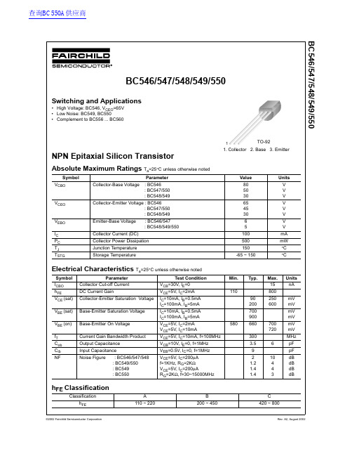
BC546/547/548/549/550NPN Epitaxial Silicon TransistorAbsolute Maximum Ratings T a =25°C unless otherwise notedElectrical Characteristics T a =25°C unless otherwise notedh FE ClassificationSymbol ParameterValue Units V CBOCollector-Base Voltage : BC546: BC547/550: BC548/549 805030V V V V CEOCollector-Emitter Voltage : BC546: BC547/550: BC548/549654530V V V V EBO Emitter-Base Voltage : BC546/547: BC548/549/55065V V I C Collector Current (DC)100mA P C Collector Power Dissipation 500mW T J Junction Temperature 150°C T STGStorage Temperature-65 ~ 150°CSymbol ParameterTest ConditionMin.Typ.Max.Units I CBO Collector Cut-off Current V CB =30V, I E =015nAh FE DC Current GainV CE =5V, I C =2mA 110800V CE (sat)Collector-Emitter Saturation Voltage I C =10mA, I B =0.5mA I C =100mA, I B =5mA 90200250600mV mV V BE (sat)Base-Emitter Saturation Voltage I C =10mA, I B =0.5mA I C =100mA, I B =5mA 700900mV mV V BE (on)Base-Emitter On Voltage V CE =5V, I C =2mA V CE =5V, I C =10mA580660700720mV mV f T Current Gain Bandwidth Product V CE =5V, I C =10mA, f=100MHz 300MHz C ob Output Capacitance V CB =10V, I E =0, f=1MHz 3.56pF C ib Input CapacitanceV EB =0.5V, I C =0, f=1MHz 9pF NFNoise Figure : BC546/547/548: BC549/550: BC549: BC550V CE =5V, I C =200µA f=1KHz, R G =2K ΩV CE =5V, I C =200µAR G =2K Ω, f=30~15000MHz21.21.41.410443dB dB dB dB ClassificationA B C h FE110 ~ 220200 ~ 450420 ~ 800BC546/547/548/549/550Switching and Applications•High Voltage: BC546, V CEO =65V •Low Noise: BC549, BC550•Complement to BC556 ... BC5601. Collector2. Base3. EmitterTO-921查询BC550A供应商BC546/547/548/549/550BC546/547/548/549/550TRADEMARKSThe following are registered and unregistered trademarks Fairchild Semiconductor owns or is authorized to use and is not intended to be an exhaustive list of all such trademarks.DISCLAIMERFAIRCHILD SEMICONDUCTOR RESERVES THE RIGHT TO MAKE CHANGES WITHOUT FURTHER NOTICE TO ANY PRODUCTS HEREIN TO IMPROVE RELIABILITY, FUNCTION OR DESIGN. FAIRCHILD DOES NOT ASSUME ANY LIABILITY ARISING OUT OF THE APPLICATION OR USE OF ANY PRODUCT OR CIRCUIT DESCRIBED HEREIN;NEITHER DOES IT CONVEY ANY LICENSE UNDER ITS PATENT RIGHTS, NOR THE RIGHTS OF OTHERS.LIFE SUPPORT POLICYFAIRCHILD’S PRODUCTS ARE NOT AUTHORIZED FOR USE AS CRITICAL COMPONENTS IN LIFE SUPPORT DEVICES OR SYSTEMS WITHOUT THE EXPRESS WRITTEN APPROVAL OF FAIRCHILD SEMICONDUCTOR CORPORATION.As used herein:1. Life support devices or systems are devices or systems which, (a) are intended for surgical implant into the body,or (b) support or sustain life, or (c) whose failure to perform when properly used in accordance with instructions for use provided in the labeling, can be reasonably expected to result in significant injury to the user.2. A critical component is any component of a life support device or system whose failure to perform can be reasonably expected to cause the failure of the life support device or system, or to affect its safety or effectiveness.PRODUCT STATUS DEFINITIONS Definition of TermsDatasheet Identification Product Status DefinitionAdvance InformationFormative or In Design This datasheet contains the design specifications for product development. Specifications may change in any manner without notice.PreliminaryFirst ProductionThis datasheet contains preliminary data, andsupplementary data will be published at a later date.Fairchild Semiconductor reserves the right to make changes at any time without notice in order to improve design.No Identification Needed Full ProductionThis datasheet contains final specifications. Fairchild Semiconductor reserves the right to make changes at any time without notice in order to improve design.Obsolete Not In ProductionThis datasheet contains specifications on a product that has been discontinued by Fairchild semiconductor.The datasheet is printed for reference information only.FACT™FACT Quiet series™FAST ®FASTr™FRFET™GlobalOptoisolator™GTO™HiSeC™I 2C™ImpliedDisconnect™ISOPLANAR™LittleFET™MicroFET™MicroPak™MICROWIRE™MSX™MSXPro™OCX™OCXPro™OPTOLOGIC ®OPTOPLANAR™PACMAN™POP™Power247™PowerTrench ®QFET™QS™QT Optoelectronics™Quiet Series™RapidConfigure™RapidConnect™SILENT SWITCHER ®SMART START™SPM™Stealth™SuperSOT™-3SuperSOT™-6SuperSOT™-8SyncFET™TinyLogic™TruTranslation™UHC™UltraFET ®VCX™ACEx™ActiveArray™Bottomless™CoolFET™CROSSVOLT ™DOME™EcoSPARK™E 2CMOS™EnSigna™Across the board. Around the world.™The Power Franchise™Programmable Active Droop™。
CS5463A
IC datasheet pdf-CD54AC273, CD74AC273,CD54ACT273, CD74ACT273,pdf(Octal D Flip-Flop)
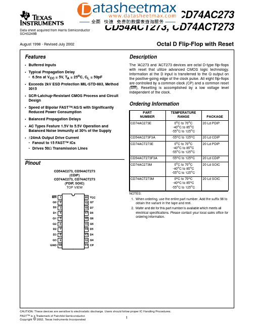
Data sheet acquired from Harris SemiconductorSCHS249BFeatures•Buffered Inputs•Typical Propagation Delay- 6.5ns at V CC = 5V , T A = 25o C, C L = 50pF•Exceeds 2kV ESD Protection MIL-STD-883, Method 3015•SCR-Latchup-Resistant CMOS Process and Circuit Design •Speed of Bipolar FAST™/AS/S with Significantly Reduced Power Consumption •Balanced Propagation Delays•AC Types Feature 1.5V to 5.5V Operation and Balanced Noise Immunity at 30% of the Supply •±24mA Output Drive Current -Fanout to 15 FAST™ ICs-Drives 50Ω Transmission LinesPinoutCD54AC273, CD54ACT273(CDIP)CD74AC273, CD74ACT273(PDIP , SOIC)TOP VIEWDescriptionThe ’AC273and ’ACT273devices are octal D-type flip-flops with reset that utilize advanced CMOS logic rmation at the D input is transferred to the Q output on the positive-going edge of the clock pulse.All eight flip-flops are controlled by a common clock (CP)and a common reset (MR).Resetting is accomplished by a low voltage level independent of the clock.1112131415161718201910987654321MR Q0D0D1Q1Q2D3D2Q3GND V CC D7D6Q6Q7Q5D5D4Q4CPOrdering InformationPART NUMBER TEMPERATURERANGE PACKAGE CD74AC273E0o C to 70o C -40o C to 85o C -55o C to 125o C 20 Ld PDIPCD54AC273F3A -55o C to 125o C 20 Ld CDIP CD74ACT273E0o C to 70o C -40o C to 85o C -55o C to 125o C 20 Ld PDIPCD54ACT273F3A -55o C to 125o C 20 Ld CDIP CD74AC273M0o C to 70o C -40o C to 85o C -55o C to 125o C 20 Ld SOICCD74ACT273M 0o C to 70o C -40o C to 85o C -55o C to 125o C20 Ld SOICNOTES:1.When ordering,use the entire part number.Add the suffix 96to obtain the variant in the tape and reel.2.Wafer and die for this part number is available which meets allelectrical specifications.Please contact your local sales office for ordering information.August 1998 - Revised July 2002CD54AC273, CD74AC273CD54ACT273, CD74ACT273Octal D Flip-Flop with ResetFunctional DiagramTRUTH TABLE INPUTSOUTPUTSRESET (MR)CLOCK CP DATA Dn Qn L X X L H ↑H H H ↑L L HLXQ0H =High level (steady state),L =Low level (steady state),X =Irrel-evant,↑=Transition from Low to High level,Q0=The level of Q before the indicated steady-state input conditions were estab-lished.Q0Q1Q2Q3Q4Q5Q6Q7RESET MRD0D1D2D3D4D5D6D7CLOCKCPDATA INPUTSDATAOUTPUTSAbsolute Maximum Ratings Thermal InformationDC Supply Voltage, V CC. . . . . . . . . . . . . . . . . . . . . . . .-0.5V to 6V DC Input Diode Current, I IKFor V I < -0.5V or V I > V CC + 0.5V. . . . . . . . . . . . . . . . . . . . . .±20mA DC Output Diode Current, I OKFor V O < -0.5V or V O > V CC + 0.5V . . . . . . . . . . . . . . . . . . . .±50mA DC Output Source or Sink Current per Output Pin, I OFor V O > -0.5V or V O < V CC + 0.5V . . . . . . . . . . . . . . . . . . . .±50mA DC V CC or Ground Current, I CC or I GND (Note 3) . . . . . . . . .±100mA Operating ConditionsTemperature Range, T A . . . . . . . . . . . . . . . . . . . . . .-55o C to 125o C Supply Voltage Range, V CC (Note 4)AC T ypes. . . . . . . . . . . . . . . . . . . . . . . . . . . . . . . . . . .1.5V to 5.5V ACT T ypes . . . . . . . . . . . . . . . . . . . . . . . . . . . . . . . . .4.5V to 5.5V DC Input or Output Voltage, V I, V O . . . . . . . . . . . . . . . . .0V to V CC Input Rise and Fall Slew Rate, dt/dvAC T ypes, 1.5V to 3V . . . . . . . . . . . . . . . . . . . . . . . . .50ns (Max) AC T ypes, 3.6V to 5.5V. . . . . . . . . . . . . . . . . . . . . . . .20ns (Max) ACT T ypes, 4.5V to 5.5V. . . . . . . . . . . . . . . . . . . . . . .10ns (Max)Thermal Resistance,θJA(Typical, Note 5)E Package. . . . . . . . . . . . . . . . . . . . . . . . . . . . . . . . . . . . .69o C/W M Package. . . . . . . . . . . . . . . . . . . . . . . . . . . . . . . . . . . . .58o C/W Maximum Junction T emperature (Plastic Package) . . . . . . . . . .150o C Maximum Storage Temperature Range . . . . . . . . . .-65o C to 150o C Maximum Lead Temperature (Soldering 10s). . . . . . . . . . . . .300o CCAUTION:Stresses above those listed in“Absolute Maximum Ratings”may cause permanent damage to the device.This is a stress only rating and operation of the device at these or any other conditions above those indicated in the operational sections of this specification is not implied.NOTES:3.For up to 4 outputs per device, add±25mA for each additional output.4.Unless otherwise specified, all voltages are referenced to ground.5.The package thermal impedance is calculated in accordance with JESD 51.DC Electrical SpecificationsPARAMETER SYMBOLTESTCONDITIONS VCC(V)25o C-40o C TO85o C-55o C TO125o CUNITS V I(V)I O(mA)MIN MAX MIN MAX MIN MAXAC TYPESHigh Level Input Voltage V IH-- 1.5 1.2- 1.2- 1.2-V3 2.1- 2.1- 2.1-V5.5 3.85- 3.85- 3.85-V Low Level Input Voltage V IL-- 1.5-0.3-0.3-0.3V3-0.9-0.9-0.9V5.5- 1.65- 1.65- 1.65V High Level Output Voltage V OH V IH or V IL-0.05 1.5 1.4- 1.4- 1.4-V-0.053 2.9- 2.9- 2.9-V-0.05 4.5 4.4- 4.4- 4.4-V-43 2.58- 2.48- 2.4-V-24 4.5 3.94- 3.8- 3.7-V-75(Note 6, 7)5.5-- 3.85---V-50(Note 6, 7)5.5---- 3.85-VLow Level Output VoltageV OLV IH or V IL0.05 1.5-0.1-0.1-0.1V 0.053-0.1-0.1-0.1V 0.05 4.5-0.1-0.1-0.1V 123-0.36-0.44-0.5V 24 4.5-0.36-0.44-0.5V 75(Note 6, 7) 5.5--- 1.65--V 50(Note 6, 7)5.5----- 1.65V Input Leakage Current I I V CC or GND - 5.5-±0.1-±1-±1µA Quiescent Supply Current MSI I CCV CC or GND5.5-8-80-160µAACT TYPESHigh Level Input Voltage V IH -- 4.5 to 5.52-2-2-V Low Level Input Voltage V IL -- 4.5 to 5.5-0.8-0.8-0.8V High Level Output VoltageV OHV IH or V IL-0.05 4.5 4.4- 4.4- 4.4-V -24 4.5 3.94- 3.8- 3.7-V -75(Note 6, 7) 5.5-- 3.85---V -50(Note 6, 7)5.5---- 3.85-V Low Level Output VoltageV OLV IH or V IL0.05 4.5-0.1-0.1-0.1V 24 4.5-0.36-0.44-0.5V 75(Note 6, 7) 5.5--- 1.65--V 50(Note 6, 7)5.5----- 1.65V Input Leakage Current I I V CC or GND - 5.5-±0.1-±1-±1µA Quiescent Supply Current MSII CC V CC or GND 0 5.5-8-80-160µA Additional Supply Current per Input Pin TTL Inputs High 1 Unit Load ∆I CCV CC -2.1- 4.5 to 5.5- 2.4- 2.8-3mANOTES:6.Test one output at a time for a 1-second maximum duration.Measurement is made by forcing current and measuring voltage to minimize power dissipation.7.Test verifies a minimum 50Ω transmission-line-drive capability at 85o C, 75Ω at 125o C.ACT Input Load TableINPUT UNIT LOADDn 0.5MR 0.57CP1NOTE:Unit load is ∆I CC limit specified in DC Electrical Specifications T able, e.g., 2.4mA max at 25o C.DC Electrical Specifications(Continued)PARAMETERSYMBOL TEST CONDITIONSV CC (V)25o C -40o C TO 85o C -55o C TO 125o C UNITS V I (V)I O (mA)MIN MAX MIN MAX MIN MAXPrerequisite For Switching FunctionPARAMETER SYMBOL V CC (V)-40o C TO 85o C-55o C TO 125o CUNITS MIN MAX MIN MAXAC TYPESData to CP Set-Up Time t SU 1.52-2-ns3.3(Note 9)2-2-ns5(Note 10)2-2-ns Hold Time t H 1.52-2-ns3.32-2-ns52-2-ns Removal Time,MR to CP t REM 1.52-2-ns3.32-2-ns52-2-ns MR Pulse Width t W 1.555-63-ns3.3 6.1-7-ns5 4.4-5-ns CP Pulse Width t W 1.555-63-ns3.3 6.1-7-ns5 4.4-5-ns CP Frequency f MAX 1.59-8-MHz3.381-71-MHz5114-100-MHz ACT TYPESData to CP Set-Up Time t SU5(Note 10)2-2-ns Hold Time t H52-2-ns Removal Time MR to CP t REM52-2-ns MR Pulse Width t W5 4.4-5-ns CP Pulse Width t W5 5.3-6-ns CP Frequency f MAX597-85-MHz Switching Specifications Input t r, t f = 3ns, C L= 50pF (Worst Case)PARAMETER SYMBOL V CC (V)-40o C TO 85o C-55o C TO 125o CUNITS MIN TYP MAX MIN TYP MAXAC TYPESPropagation Delay, CP to Qn t PLH, t PHL 1.5--154--169ns3.3(Note 9)4.9-17.2 4.7-18.9ns5(Note 10)3.5-12.3 3.4-13.5nsPropagation Delay,MR to Qnt PLH , t PHL1.5--154--169ns 3.3 4.9-17.2 4.7-18.9ns 53.5-12.3 3.4-13.5ns Input CapacitanceC I ---10--10pF Power Dissipation Capacitance C PD (Note 11)--45--45-pFACT TYPES Propagation Delay,CP to Qnt PLH , t PHL 5(Note 10)3.5-12.3 3.4-13.5ns Propagation Delay,MR to Qn t PLH , t PHL5 3.5-12.3 3.4-13.5ns Input CapacitanceC I ---10--10pF Power Dissipation Capacitance C PD (Note 11)--45--45-pFNOTES:8.Limits tested 100%.9.3.3V Min is at 3.6V, Max is at 3V.10.5V Min is at 5.5V, Max is at 4.5V.11.C PD is used to determine the dynamic power consumption per flip-flop.AC: P D = C PD V CC 2 f i =∑ (C L V CC 2 f o )ACT:P D =C PD V CC 2f i +∑(C L V CC 2f o )+V CC ∆I CC where f i =input frequency,f o =output frequency,C L =output load capacitance,V CC = supply voltage.FIGURE 1.PROPAGATION DELAY TIMES AND CLOCKPULSE WIDTH FIGURE 2.PREREQUISITE AND PROPAGATION DELAYTIMES FOR MASTER RESETSwitching Specifications Input t r , t f = 3ns, C L = 50pF (Worst Case)(Continued)PARAMETERSYMBOL V CC (V)-40o C TO 85o C-55o C TO 125o CUNITS MIN TYP MAX MIN TYP MAX 90%t f t r V SV S V SV SV St PLHt PHLt W 10%10%CP INPUT LEVEL QMR CPINPUT LEVELV SQV St REMV SV St PLHt WGNDINPUT(Q)FIGURE 3.PREREQUISITE FOR CLOCKDV S V S V SV S V S V St H (H)t SU (L)t H (L)t SU (H)CPOUTPUT LEVELDUT OUTPUTR L (NOTE)OUTPUT LOAD500ΩC L 50pFNOTE:For AC Series Only: When V CC = 1.5V , R L = 1k Ω.FIGURE 4.PROPAGATION DELAY TIMESACACT Input LevelV CC 3V Input Switching Voltage, V S 0.5 V CC 1.5V Output Switching Voltage, V S0.5 V CC0.5 V CCPACKAGING INFORMATIONOrderable Device Status(1)PackageType PackageDrawingPins PackageQtyEco Plan(2)Lead/Ball Finish MSL Peak Temp(3)CD54AC273F3A ACTIVE CDIP J201TBD A42N/A for Pkg Type CD54ACT273F3A ACTIVE CDIP J201TBD A42N/A for Pkg Type CD74AC273E ACTIVE PDIP N2020Pb-Free(RoHS)CU NIPDAU N/A for Pkg TypeCD74AC273EE4ACTIVE PDIP N2020Pb-Free(RoHS)CU NIPDAU N/A for Pkg TypeCD74AC273M ACTIVE SOIC DW2025Green(RoHS&no Sb/Br)CU NIPDAU Level-1-260C-UNLIMCD74AC273M96ACTIVE SOIC DW202000Green(RoHS&no Sb/Br)CU NIPDAU Level-1-260C-UNLIMCD74AC273M96E4ACTIVE SOIC DW202000Green(RoHS&no Sb/Br)CU NIPDAU Level-1-260C-UNLIMCD74AC273M96G4ACTIVE SOIC DW202000Green(RoHS&no Sb/Br)CU NIPDAU Level-1-260C-UNLIMCD74AC273ME4ACTIVE SOIC DW2025Green(RoHS&no Sb/Br)CU NIPDAU Level-1-260C-UNLIMCD74AC273MG4ACTIVE SOIC DW2025Green(RoHS&no Sb/Br)CU NIPDAU Level-1-260C-UNLIMCD74ACT273E ACTIVE PDIP N2020Pb-Free(RoHS)CU NIPDAU N/A for Pkg TypeCD74ACT273EE4ACTIVE PDIP N2020Pb-Free(RoHS)CU NIPDAU N/A for Pkg TypeCD74ACT273M ACTIVE SOIC DW2025Green(RoHS&no Sb/Br)CU NIPDAU Level-1-260C-UNLIMCD74ACT273M96ACTIVE SOIC DW202000Green(RoHS&no Sb/Br)CU NIPDAU Level-1-260C-UNLIMCD74ACT273M96E4ACTIVE SOIC DW202000Green(RoHS&no Sb/Br)CU NIPDAU Level-1-260C-UNLIMCD74ACT273M96G4ACTIVE SOIC DW202000Green(RoHS&no Sb/Br)CU NIPDAU Level-1-260C-UNLIMCD74ACT273ME4ACTIVE SOIC DW2025Green(RoHS&no Sb/Br)CU NIPDAU Level-1-260C-UNLIMCD74ACT273MG4ACTIVE SOIC DW2025Green(RoHS&no Sb/Br)CU NIPDAU Level-1-260C-UNLIMCD74ACT273PW ACTIVE TSSOP PW2070Green(RoHS&no Sb/Br)CU NIPDAU Level-1-260C-UNLIMCD74ACT273PWE4ACTIVE TSSOP PW2070Green(RoHS&no Sb/Br)CU NIPDAU Level-1-260C-UNLIMCD74ACT273PWG4ACTIVE TSSOP PW2070Green(RoHS&no Sb/Br)CU NIPDAU Level-1-260C-UNLIMCD74ACT273PWR ACTIVE TSSOP PW202000Green(RoHS&no Sb/Br)CU NIPDAU Level-1-260C-UNLIMCD74ACT273PWRE4ACTIVE TSSOP PW202000Green(RoHS&no Sb/Br)CU NIPDAU Level-1-260C-UNLIMCD74ACT273PWRG4ACTIVE TSSOP PW202000Green(RoHS&no Sb/Br)CU NIPDAU Level-1-260C-UNLIMCD74ACT273SM96ACTIVE SSOP DB202000Green(RoHS&no Sb/Br)CU NIPDAU Level-1-260C-UNLIMCD74ACT273SM96E4ACTIVE SSOP DB202000Green(RoHS&CU NIPDAU Level-1-260C-UNLIMOrderable Device Status(1)PackageType PackageDrawingPins PackageQtyEco Plan(2)Lead/Ball Finish MSL Peak Temp(3)no Sb/Br)CD74ACT273SM96G4ACTIVE SSOP DB202000Green(RoHS&no Sb/Br)CU NIPDAU Level-1-260C-UNLIM(1)The marketing status values are defined as follows:ACTIVE:Product device recommended for new designs.LIFEBUY:TI has announced that the device will be discontinued,and a lifetime-buy period is in effect.NRND:Not recommended for new designs.Device is in production to support existing customers,but TI does not recommend using this part in a new design.PREVIEW:Device has been announced but is not in production.Samples may or may not be available.OBSOLETE:TI has discontinued the production of the device.(2)Eco Plan-The planned eco-friendly classification:Pb-Free(RoHS),Pb-Free(RoHS Exempt),or Green(RoHS&no Sb/Br)-please check /productcontent for the latest availability information and additional product content details.TBD:The Pb-Free/Green conversion plan has not been defined.Pb-Free(RoHS):TI's terms"Lead-Free"or"Pb-Free"mean semiconductor products that are compatible with the current RoHS requirements for all6substances,including the requirement that lead not exceed0.1%by weight in homogeneous materials.Where designed to be soldered at high temperatures,TI Pb-Free products are suitable for use in specified lead-free processes.Pb-Free(RoHS Exempt):This component has a RoHS exemption for either1)lead-based flip-chip solder bumps used between the die and package,or2)lead-based die adhesive used between the die and leadframe.The component is otherwise considered Pb-Free(RoHS compatible)as defined above.Green(RoHS&no Sb/Br):TI defines"Green"to mean Pb-Free(RoHS compatible),and free of Bromine(Br)and Antimony(Sb)based flame retardants(Br or Sb do not exceed0.1%by weight in homogeneous material)(3)MSL,Peak Temp.--The Moisture Sensitivity Level rating according to the JEDEC industry standard classifications,and peak solder temperature.Important Information and Disclaimer:The information provided on this page represents TI's knowledge and belief as of the date that it is provided.TI bases its knowledge and belief on information provided by third parties,and makes no representation or warranty as to the accuracy of such information.Efforts are underway to better integrate information from third parties.TI has taken and continues to take reasonable steps to provide representative and accurate information but may not have conducted destructive testing or chemical analysis on incoming materials and chemicals.TI and TI suppliers consider certain information to be proprietary,and thus CAS numbers and other limited information may not be available for release.In no event shall TI's liability arising out of such information exceed the total purchase price of the TI part(s)at issue in this document sold by TI to Customer on an annual basis.TAPE AND REELINFORMATION*All dimensionsare nominalDevicePackage Type Package Drawing Pins SPQReel Diameter (mm)Reel Width W1(mm)A0(mm)B0(mm)K0(mm)P1(mm)W (mm)Pin1Quadrant CD74AC273M96SOIC DW 202000330.024.410.813.0 2.712.024.0Q1CD74ACT273M96SOIC DW 202000330.024.410.813.0 2.712.024.0Q1CD74ACT273PWR TSSOP PW 202000330.016.4 6.957.1 1.68.016.0Q1CD74ACT273SM96SSOPDB202000330.016.48.27.52.512.016.0Q1PACKAGE MATERIALS INFORMATION11-Mar-2008*Alldimensions are nominal DevicePackage Type Package Drawing Pins SPQ Length (mm)Width (mm)Height (mm)CD74AC273M96SOIC DW 202000346.0346.041.0CD74ACT273M96SOIC DW 202000346.0346.041.0CD74ACT273PWRTSSOP PW 202000346.0346.033.0CD74ACT273SM96SSOP DB 202000346.0346.033.0PACKAGE MATERIALS INFORMATION 11-Mar-2008Pack Materials-Page 2IMPORTANT NOTICETexas Instruments Incorporated and its subsidiaries(TI)reserve the right to make corrections,modifications,enhancements,improvements, and other changes to its products and services at any time and to discontinue any product or service without notice.Customers should obtain the latest relevant information before placing orders and should verify that such information is current and complete.All products are sold subject to TI’s terms and conditions of sale supplied at the time of order acknowledgment.TI warrants performance of its hardware products to the specifications applicable at the time of sale in accordance with TI’s standard warranty.Testing and other quality control techniques are used to the extent TI deems necessary to support this warranty.Except where mandated by government requirements,testing of all parameters of each product is not necessarily performed.TI assumes no liability for applications assistance or customer product design.Customers are responsible for their products and applications using TI components.To minimize the risks associated with customer products and applications,customers should provide adequate design and operating safeguards.TI does not warrant or represent that any license,either express or implied,is granted under any TI patent right,copyright,mask work right, or other TI intellectual property right relating to any combination,machine,or process in which TI products or services are rmation published by TI regarding third-party products or services does not constitute a license from TI to use such products or services or a warranty or endorsement e of such information may require a license from a third party under the patents or other intellectual property of the third party,or a license from TI under the patents or other intellectual property of TI.Reproduction of TI information in TI data books or data sheets is permissible only if reproduction is without alteration and is accompanied by all associated warranties,conditions,limitations,and notices.Reproduction of this information with alteration is an unfair and deceptive business practice.TI is not responsible or liable for such altered rmation of third parties may be subject to additional restrictions.Resale of TI products or services with statements different from or beyond the parameters stated by TI for that product or service voids all express and any implied warranties for the associated TI product or service and is an unfair and deceptive business practice.TI is not responsible or liable for any such statements.TI products are not authorized for use in safety-critical applications(such as life support)where a failure of the TI product would reasonably be expected to cause severe personal injury or death,unless officers of the parties have executed an agreement specifically governing such use.Buyers represent that they have all necessary expertise in the safety and regulatory ramifications of their applications,and acknowledge and agree that they are solely responsible for all legal,regulatory and safety-related requirements concerning their products and any use of TI products in such safety-critical applications,notwithstanding any applications-related information or support that may be provided by TI.Further,Buyers must fully indemnify TI and its representatives against any damages arising out of the use of TI products in such safety-critical applications.TI products are neither designed nor intended for use in military/aerospace applications or environments unless the TI products are specifically designated by TI as military-grade or"enhanced plastic."Only products designated by TI as military-grade meet military specifications.Buyers acknowledge and agree that any such use of TI products which TI has not designated as military-grade is solely at the Buyer's risk,and that they are solely responsible for compliance with all legal and regulatory requirements in connection with such use. TI products are neither designed nor intended for use in automotive applications or environments unless the specific TI products are designated by TI as compliant with ISO/TS16949requirements.Buyers acknowledge and agree that,if they use any non-designated products in automotive applications,TI will not be responsible for any failure to meet such requirements.Following are URLs where you can obtain information on other Texas Instruments products and application solutions:Products ApplicationsAmplifiers AudioData Converters AutomotiveDLP®Products BroadbandDSP Digital ControlClocks and Timers MedicalInterface MilitaryLogic Optical NetworkingPower Mgmt SecurityMicrocontrollers TelephonyRFID Video&ImagingRF/IF and ZigBee®Solutions WirelessMailing Address:Texas Instruments,Post Office Box655303,Dallas,Texas75265Copyright©2009,Texas Instruments Incorporated。
2N5460中文资料
D
NOTE: Source & Drain are interchangeable
P-Channel General Purpose Amplifier
This device is designed primarily for low level audio and general purpose applications with high impedance signal sources. Sourced from Process 89.
5
Power Dissipation vs. Ambient Temperature
P D - POWER DISSIPATION (mW) 350 300 250 200 150 100 50 0 0 25 50 75 100 TEMPERATURE (ºC) 125 150
TO-92 SOT-23
元器件交易网
2N5460 / 5461 / 5462 / MMBF5460 / MMBF5461 / MMBF5462
P-Channel General Purpose Amplifier
(continued)
Electrical Characteristics
Symbol Parameter
元器件交易网
TRADEMARKS
The following are registered and unregistered trademarks Fairchild Semiconductor owns or is authorized to use and is not intended to be an exhaustive list of all such trademarks.
Agilent 54620A C 复杂版型式数字波形捕捉设备说明书
Do you use your scope as your pri-mary tool for troubleshooting digital circuits because you feel that your problems are not complex enough for a logic analyzer? Do you wish that your scope had the power of a logic analyzer without the complexity and cost of one?If so, these are the logic analyzers for you. With familiar scope-like opera-tion and high speed display, these are logic analyzers that you can simply set on your bench and use like your scope. Because you are a scope user, these are the logic analyzers that you already know how to operate.The Agilent Technologies 54620A/C is designed to be used with your scope to quickly troubleshoot and debug your mixed signal and digital circuits. The 54620A is the choice for tight budget situations. Its monochrome raster CRT display provides bright crisp displays of our logic waveforms. The 54620C adds a full-color active matrix LCD display. With the addi-tion of color, the logic analyzer’s16-channel display is easy to use. Colors can be used to group or high-light channels.The Agilent 54620A/C offers:• Scope-like control knobs• Auto scale for one button set-up• Trigger Input/outputs for usewith your scope• Automatic measurements offrequency, period, duty cycle,width, channel-to-channel delay,hold time, and set-up time• Cursor measurements andread-out of waveform values inHex or Binary• Edge, pattern, and advancedtriggering• Store/recall of 16 front panelsetups with channel labels• Full-color active matrix LCDdisplay (54620C)• Monochrome raster CRT display(54620A)• Optional GPIB or RS-232remote control• Optional hard copy to GPIB,RS-232, or parallel printers• Weight 6.8 kg/15 lb.• 3-Year WarrantyScope-like operationThe Agilent 54620A/C logic analyzersare designed for the person whoseprimary analysis tool is the oscillo-scope, but often wishes for the addi-tional power of a logic analyzer. Thislogic analyzer has a control panelthat is very much like that of yourscope. Simply turn a knob, much likeyou would on your scope, to makea change in the time per division orreposition a channel in the display.Analyzer set-up is simplified with apowerful Autoscale operation. Auto-scale will turn on and display allchannels that have activity. The timebase will be set to give an optimallyscaled display of all active signals.Flexible triggeringThe simplest and most scope-like trig-gering is provided in the edge trigger-ing mode. The pattern mode extendsthe triggering to be a pattern of high,low, and “don’t care”levels acrossall 16 of the 54620A’s input channelsas well as the external trigger inputport. This pattern can be qualified Agilent 54620A/C Logic AnalyzersProduct Overview•16 Channels•500 MSa/s• 3.5 ns Glitch Capture•Simple Scope-Like Operation•Full-Color Display with 54620Cwith an edge. For those applications where more triggering power is needed to isolate the event of interest, the Advanced trigger mode is available. High speed displayAn important consideration of a troubleshooting tool is its abilityto clearly display changes in the circuit under test. The 54620A/C employs an advanced four processor architecture, giving you a logic ana-lyzer that can display changing wave-forms in your system that would be missed by more traditional analyzers. Another benefit of the high speed display system is that the 54620A/C will respond instantly to your front panel control inputs. This eliminates a source of confusion in your trou-bleshooting process.See more with colorThe display of 16 logic channels can be somewhat confusing. By the use of color, you can group channels that are displaying related information, or specific channels can be highlighted. For example, address lines can bein one color while control lines are displayed in other colors. Alternate palettes allow the display to be cus-tomized for most favorable viewing. Upgrade to meet your changing needs You can upgrade the Agilent 54620A logic analyzer to produce hard copies to either printer or plotter Or, you can interface it to a computer with either GPIB or RS-232 interfaces. Using the HP 34810B BenchLink Scope for Windows, you can easily upload the logic analyzer display to your personal computer for preparing a report, creating a presentation,or storing the analyzer’s set-up for later use.Input ChannelsNumber of Channels16 numbered 0–15Channel Input Cable54620-61801 withchannels grouped in twosets of 8. Instrumentis compatible with0650-61607 cable andaccessories.Input R&C~100kΩand 8pFMaximum Input±40 VDynamic Range±10 V about thresholdMinimum Input500 mV peak to peakabout thresholdMinimum Input To meet timing accuracy,Voltage Overdrive the threshold value mustbe within 20% of the 50%value of the input signalThreshold Setting Threshold levels can beassigned to the inputchannels in groups of8channels (0–7 and 8–15)and external triggerThreshold Accuracy±(13% of setting±100 mV)Preset Threshold Levels TTL—1.5 VCMOS—2.5VECL—1.3 VChannel to Channel Skew2.0 ns typical3.0 ns maximumHorizontal SystemSweep Speeds 1 s/div to 5 ns/divMain & Delayed SweepExtended to 5s/div withAutoglitch disabledAccuracy001% of readingMain, Delayed sweeps,and verniersHorizontal Modes Main, Main and Delayedand post acquisition panand zoomCursor AccuracySingle Channel±(Sample Period + 0.05%of reading + 0.2% ofscreen width)Dual Channel±(Sample Period + Chto Ch skew + 0.01% ofreading + 0.2% of screenwidth)Delay Jitter10 ppmDelay Range Pretrigger (Negative time)Maximum delay is independent of time reference(left, center, right)Sweep Speed Maximum delay(per division)divisions5 ns3,23110 ns1,61520 ns80750 ns323100 ns161200 ns80.7500 ns64.61 µs16> 1 µs16Post-Trigger(from trigger point tostart of sweep) from5 ns/div to 1µs/div—8.829 msFrom 2 ms/div to 1 s/div—1,048,575 timessampling period, not toexceed 100 s.Delayed Sweep Delayed can be as fastOperation as 5 ns/div but must beat least 2X main sweep.Post Acquisition Acquired waveformsPan & Zoom Operation may be panned acrossthe display and/orexpanded for enhancedviewing by simplychanging time/div ordelay settings.Acquisition SystemMaximum Sample Rate500 MSalsResolution Single bitSimultaneous Channels16Record Length 2 k samples at periodsof 8ns and slower(sweep speeds of1 µs/div to 1s/div) 8 ksamples at samplingperiods of 2 ns and 4 ns(sweep speeds of 5 ns/divto 500 ns/div), or allsweep speeds whenAutoglitch mode isdisabledMaximum Update Rate15 full screens persecond independent ofthe number of channelsbeing displayed.Glitch Detect Automatically activatedat all sweep speedswhere sampling periodis slowed to be greaterthan 4 ns (1µs/div andslower). Will detectglitches as narrow as3.5 ns at all activatedsweep speeds.Trigger SystemSources All Channels & ExternalAuto/Normal Operation Auto will produce afree running display ifthe trigger is not found.Normal causes theanalyzer to waitindefinitely for a triggerto start acquiring data.Modes: Edge, Pattern and AdvancedEdge A single edge can bespecified on channels0–15 and External.Edge may be rising,falling, or either.2Pattern Analyzer will triggerupon entering a patternof high, low and don'tcare levels on all of thechannels and externaltrigger input. A singleedge (rising, falling, oreither) can be ANDedand this pattern. Advanced Two unique patternand edge terms can becombined with operationsto create a very specifictrigger event. Advanced Operators And, Or, Then, Entered,Exited, Duration> time,Duration < time, andOccurs N times. MaximumOccurrence: 220-1Edge Recovery Sweep speeds of 5 ns/divto 1 µs/div: 28 ns Sweepspeeds of 2 µs/div andslower: 20 ns + 1sample period Minimum Detection13 ns + Ch to Ch skew Pattern Width at sweep speeds of5 ns/div to 1 µs/div.At sweep speeds of2 µds/div and slower =(1ns + 1 sample period+ Ch to Ch skew + 0.01%) Minimum Settable At all sweep = 2 sample Duration periods of 16 nss,whichever is greater. External triggerInput R & C~ 1 mΩand 12 pF.Compatible with1007X probes. Maximum Input±40 V peakTrigger Threshold+ 6 V, settable in 50 mV IncrementsThreshold Accuracy+ 100 mV or 6% of settingwhichever is greater Minimum Input Change200 mV ppMinimum Pulse Width20 nsTrigger Output Output is a rising edgeat the trigger point. Output Level0 to >/=2.0 v into 50Ω0 to >/=4.8 V open circuit Delay Data in to trigger out~ 85 nsJitter±(Sample period + 10 ppm) Maximum Output Rate 2 kHz with the analyzerstopped, 20/sec running. Display SystemDisplay54610A: 7" RasterCRT 54620C: 5.8"active matrix color LCD Resolution256 Vertical by 500Horizontal points Controls Graticule Front panel intensitycontrol Selectable 8 x 10grid frame, or none Storage Scope Autostore saves previoussweeps in half brightdisplay and the mostrecent sweep full brightdisplay. This allowseasy differentiation ofcurrent and historicinformation.Measurement FunctionsAutomatic The analyzer will performMeasurements measurements on theselected input channel(s).These measurementsare continuously updated.Single Channel Frequency, Period,+ Width, - Width, andDuty CycleDual Channel Channel to Channeldelay, Hold-time, andSet-up time.Cursor Measurements Two cursors can bepositioned on thedisplay to make timemeasurements or readthe value of the waveforms at the center.The cursors will trackchanges in time/divand delay controls.Readout in Time,1/Time, Hex, and Binary.Set-up FunctionsAutoscale Selects all activechannels and placesthem in the display.Channels not previouslydisplayed will be addedbelow those channelsalready being displayedwith the lowest numberedchannel at the top.Higher numbered channelswill be displayed in orderdown the display.Sweep speed is set togive an optimally scaleddisplay of all the activechannels. Triggeringand ___are not affected.Requires a signal with> 49 Hz frequency.Undo Autoscale functionreturns the instrumentto the set-up prior toAutoscale being activated.Save/Recall16 front panel set-upscan be stored and recalledfrom nonvolatile memory.Trace Memory Two volatile pixel memo-ries allow storage oftrace display waveforms.Channel Label s Each channel may beidentified with a sixcharacter label. Labelscan be created from afront panel label genera-tor and a library of up to75 present and userdefined labels.Probe Calibrator Amplitude 5.0 V,Frequency9.8 kHzPower RequirementsVoltage selection AutomaticLine Voltage Range90 to 250 VacLine Frequency48 to 445 HzMax. Power 100 VAConsumptionGeneralEnvironmental Meets the requirementsCharacteristics of MIL-T-28800D forType III, Class 3, Style Dequipment as describedbelow:Ambient TemperatureOperating:-10°C to +55°CNonoperating:-51°C to +71°CHumidity*Operating:95% RH at 40°C for24hoursNonoperating:90% RH at 65°Cfor 24hours*Tested to Hewlett-Packard environmentalspecification section 758 for call B-1 productsAltitudeOperating:To 4,500 m (15,000 ft)Nonoperating:To 15,000 m (50,000 ft)Vibration Operating15 min along each of thethree major axes;0.025-in peak to peakdisplacement, 10 Hz to55 Hzs in 1 minutecycles. Held at 10 min at55Hz (4 g at 55 Hz)Shock Operating30 g. 1/2 sine, T1-msduration. 3 shocks/axisalong major axis. Totalof 18 shock.EMICommercial Meets CISPR 11 Class AMIL-T-28800D Meets the requirementsin accordance withMIL-T-28800 paragraph3.8.3 table IX, andMIL-STD-461CCE01:Part 2CE03:Part 2CS01:Part 2CS02:Part 2 (limitedto100 MHz)CS06:Part 5RE01: Part 5 measured at 6 inches,15 dB exceptioned from 19 kHz to 50 kHzRE02: Part 2 (limited to 1 GHz) 10 dB relaxation,14kHz to 100 kHzRS03: Part 2, limited to 3 V/meter from14 kHz to 1GHz.This product meets the requirement of theEuropean Communities (EC) EMC Directive89/336/EEC.Emissions:EN55011/CISPR 11(ISM, Group 1, Class A equipment)3Ordering Information54620A16-channel 500 MSa Logic Analyzer(supplied with 16-channel input cable assembly, User and Service Guide,as specified by language option) and line cord54820C Color 16-channel 500 MSa Logic Analyzer(supplied with 16-channel input cable assembly, User and Service Guide,as specified by language option) and line cordManual Language Options (please specify one)ABA US English ABF French ABO Taiwan ChineseABD German ABJ Japanese AB1 KoreanABE Spanish ABZ ItalianInstrument OptionsOpt. 101Accessory Pouch and Front Panel CoverOpt. 10354654A Operator’s Training Kitconsists of a training signal board and lab workbookOpt. 1041185A Carrying Case(designed to protect the instrument for shipment or checking as airline baggage) Opt. 106HP 34810B BenchLink scope software.Windows software that interfaces the instrument (with a GPIB or RS-232 module installed) to a PC for storage, analysis, or easy integration of trace images into popular desktop publishing software.Opt. 001RS-03 Magnetic shielding (added to the CRT)(not compatible with the 54620C)Opt. 1CM Rackmount Kit, seven-inch EIA standard rack mount p/n 5062-7345, compatible with fixed or pivoted slidesOptional Accessories54650A GPIB Interface Module54652RS-232 and Parallel Interface Module10070A1.4 m 1X oscilloscope probe10071A1.5 m 150 MHz 10X oscilloscope probe10072A probe adapter kit for 1007X Probes01650-6160716-Channel Woven Probe Cable, compatible with1251-8106 20-pin header01650-6160816-Channel Probe Lead Set for use with 01650-61607 cableE2421A SOIC Clip Adapter KitE2422A J lead plastic lead clip carrier test kit Agilent Technologies’ Test and Measurement Support, Services, and AssistanceAgilent Technologies aims to maximize the value you receive, while minimizing your risk and problems. We strive to ensure that you get the test and measure-ment capabilities you paid for and obtain the support you need. Our extensive sup-port resources and services can help you choose the right Agilent products for your applications and apply them successfully. Every instrument and system we sell has a global warranty. Support is availablefor at least five years beyond the produc-tion life of the product. Two concepts underlie Agilent’s overall support policy:“Our Promise” and “Your Advantage.”Our Promise“Our Promise” means your Agilent test and measurement equipment will meet its advertised performance and functionality. When you are choosing new equipment, we will help you with product informa-tion, including realistic performance spec-ifications and practical recommendations from experienced test engineers. When you use Agilent equipment, we can verify that it works properly, help with product operation, and provide basic measurement assistance for the use of specified capabil-ities, at no extra cost upon request. Many self-help tools are available.Your Advantage“Your Advantage” means that Agilent offers a wide range of additional expert test and measurement services, which you can purchase according to your unique technical and business needs. Solve prob-lems efficiently and gain a competitive edge by contracting with us for calibration,extra-cost upgrades, out-of-warranty repairs, and on-site education and training, as wellas design, system integration, project man-agement, and other professional services. Experienced Agilent engineers and techni-cians worldwide can help you maximize your productivity, optimize the return on investment of your Agilent instruments and systems, and obtain dependable measure-ment accuracy for the life of those products. Get assistance with all yourtest and measurement needs at:/find/assistProduct specifications and descriptions inthis document subject to change without notice. Copyright © 1998, 2000 Agilent Technologies Printed in U.S.A. 4/005968-2614ENImmunityEN50082-1 Code1Notes2 IEC, 801-2 (ESD) 4kV CD, SkV AD1 A IEC 801-3 (Rad.) 3V/m1 A IEC 801-4 (EFT) 1kV1 B SizeHeight:172.7 mm (6.8 in) Width:322.6 mm (12.7 in) Depth:317.5 mm (12.5 in) Weight: 6.8 Kg (15 lb)Safety Self-certified to IEC348/HD401, UL 1244,CSA-C22 No. 231(series M-89)1Performance Code1 PASS—Normal operation, no effect.2 PASS—Temporary degradation, self-recoverable.3 PASS—Temporary degradation, operator interventionrequired.4 PASS—Not recoverable, component damage.2NotesA TTL logic threshold with all cables disconnected.B TTL logic threshold with GPIB cable connected.。
IC datasheet pdf-TPIC6A259,pdf (Power Logic 8-Bit Addressable Latch)
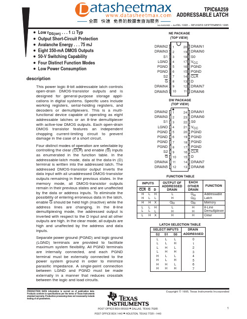
POWER LOGIC 8ĆBIT ADDRESSABLE LATCHPOWER LOGIC 8ĆBIT ADDRESSABLE LATCHPOWER LOGIC 8ĆBIT ADDRESSABLE LATCHPOWER LOGIC 8ĆBIT ADDRESSABLE LATCHPOWER LOGIC 8ĆBIT ADDRESSABLE LATCHPACKAGING INFORMATION Orderable DeviceStatus (1)Package Type Package Drawing Pins Package Qty Eco Plan (2)Lead/Ball Finish MSL Peak Temp (3)TPIC6A259DWACTIVE SOIC DW 2425TBD CU NIPDAU Level-1-220C-UNLIM TPIC6A259DWG4ACTIVE SOIC DW 2425Green (RoHS &no Sb/Br)CU NIPDAU Level-1-260C-UNLIM TPIC6A259DWRG4ACTIVE SOIC DW 242000Green (RoHS &no Sb/Br)CU NIPDAU Level-1-260C-UNLIM TPIC6A259NEACTIVE PDIP NE 2020Pb-Free (RoHS)CU NIPDAU N /A for Pkg Type (1)The marketing status values are defined as follows:ACTIVE:Product device recommended for new designs.LIFEBUY:TI has announced that the device will be discontinued,and a lifetime-buy period is in effect.NRND:Not recommended for new designs.Device is in production to support existing customers,but TI does not recommend using this part in a new design.PREVIEW:Device has been announced but is not in production.Samples may or may not be available.OBSOLETE:TI has discontinued the production of the device.(2)Eco Plan -The planned eco-friendly classification:Pb-Free (RoHS),Pb-Free (RoHS Exempt),or Green (RoHS &no Sb/Br)-please check /productcontent for the latest availability information and additional product content details.TBD:The Pb-Free/Green conversion plan has not been defined.Pb-Free (RoHS):TI's terms "Lead-Free"or "Pb-Free"mean semiconductor products that are compatible with the current RoHS requirements for all 6substances,including the requirement that lead not exceed 0.1%by weight in homogeneous materials.Where designed to be soldered at high temperatures,TI Pb-Free products are suitable for use in specified lead-free processes.Pb-Free (RoHS Exempt):This component has a RoHS exemption for either 1)lead-based flip-chip solder bumps used between the die and package,or 2)lead-based die adhesive used between the die and leadframe.The component is otherwise considered Pb-Free (RoHS compatible)as defined above.Green (RoHS &no Sb/Br):TI defines "Green"to mean Pb-Free (RoHS compatible),and free of Bromine (Br)and Antimony (Sb)based flame retardants (Br or Sb do not exceed 0.1%by weight in homogeneous material)(3)MSL,Peak Temp.--The Moisture Sensitivity Level rating according to the JEDEC industry standard classifications,and peak solder temperature.Important Information and Disclaimer:The information provided on this page represents TI's knowledge and belief as of the date that it is provided.TI bases its knowledge and belief on information provided by thirdparties,and makes no representation or warranty as to the accuracy of such information.Efforts are underway to better integrate information from third parties.TI has taken and continues to take reasonable steps to provide representative and accurate information but may not have conducted destructive testing or chemical analysis on incoming materials and chemicals.TI and TI suppliers consider certain information to be proprietary,and thus CAS numbers and other limited information may not be available for release.In no event shall TI's liability arising out of such information exceed the total purchase price of the TI part(s)at issue in this document sold by TI to Customer on an annual basis.PACKAGE OPTION ADDENDUM 28-May-2009Addendum-Page 1IMPORTANT NOTICETexas Instruments Incorporated and its subsidiaries(TI)reserve the right to make corrections,modifications,enhancements,improvements, and other changes to its products and services at any time and to discontinue any product or service without notice.Customers should obtain the latest relevant information before placing orders and should verify that such information is current and complete.All products are sold subject to TI’s terms and conditions of sale supplied at the time of order acknowledgment.TI warrants performance of its hardware products to the specifications applicable at the time of sale in accordance with TI’s standard warranty.Testing and other quality control techniques are used to the extent TI deems necessary to support this warranty.Except where mandated by government requirements,testing of all parameters of each product is not necessarily performed.TI assumes no liability for applications assistance or customer product design.Customers are responsible for their products and applications using TI components.To minimize the risks associated with customer products and applications,customers should provide adequate design and operating safeguards.TI does not warrant or represent that any license,either express or implied,is granted under any TI patent right,copyright,mask work right, or other TI intellectual property right relating to any combination,machine,or process in which TI products or services are rmation published by TI regarding third-party products or services does not constitute a license from TI to use such products or services or a warranty or endorsement e of such information may require a license from a third party under the patents or other intellectual property of the third party,or a license from TI under the patents or other intellectual property of TI.Reproduction of TI information in TI data books or data sheets is permissible only if reproduction is without alteration and is accompanied by all associated warranties,conditions,limitations,and notices.Reproduction of this information with alteration is an unfair and deceptive business practice.TI is not responsible or liable for such altered rmation of third parties may be subject to additional restrictions.Resale of TI products or services with statements different from or beyond the parameters stated by TI for that product or service voids all express and any implied warranties for the associated TI product or service and is an unfair and deceptive business practice.TI is not responsible or liable for any such statements.TI products are not authorized for use in safety-critical applications(such as life support)where a failure of the TI product would reasonably be expected to cause severe personal injury or death,unless officers of the parties have executed an agreement specifically governing such use.Buyers represent that they have all necessary expertise in the safety and regulatory ramifications of their applications,and acknowledge and agree that they are solely responsible for all legal,regulatory and safety-related requirements concerning their products and any use of TI products in such safety-critical applications,notwithstanding any applications-related information or support that may be provided by TI.Further,Buyers must fully indemnify TI and its representatives against any damages arising out of the use of TI products in such safety-critical applications.TI products are neither designed nor intended for use in military/aerospace applications or environments unless the TI products are specifically designated by TI as military-grade or"enhanced plastic."Only products designated by TI as military-grade meet military specifications.Buyers acknowledge and agree that any such use of TI products which TI has not designated as military-grade is solely at the Buyer's risk,and that they are solely responsible for compliance with all legal and regulatory requirements in connection with such use. TI products are neither designed nor intended for use in automotive applications or environments unless the specific TI products are designated by TI as compliant with ISO/TS16949requirements.Buyers acknowledge and agree that,if they use any non-designated products in automotive applications,TI will not be responsible for any failure to meet such requirements.Following are URLs where you can obtain information on other Texas Instruments products and application solutions:Products ApplicationsAmplifiers AudioData Converters AutomotiveDLP®Products BroadbandDSP Digital ControlClocks and Timers MedicalInterface MilitaryLogic Optical NetworkingPower Mgmt SecurityMicrocontrollers TelephonyRFID Video&ImagingRF/IF and ZigBee®Solutions WirelessMailing Address:Texas Instruments,Post Office Box655303,Dallas,Texas75265Copyright©2009,Texas Instruments Incorporated。
NTE5461中文资料

NTE5461 thru NTE5468Silicon Controlled Rectifier (SCR)10 AmpDescription:The NTE5461 through NTE5468 series silicon controlled rectifiers are designed primarily for half–wave AC control applications such as motor controls, heating controls, and power supplies; or wher-ever half–wave silicon gate–controlled, solid–state devices are needed. These devices are supplied in a TO220 type package.Features;D Glass Passivated Junctions and Center Gate Fire for Greater Parameter Uniformity and Stability D Small, Rugged, Thermowatt Construction for Low Thermal Resistance, High Heat Dissipation,and DurabilityD Blocking Voltage to 800 VoltsAbsolute Maximum Ratings:Peak Repetitive Reverse Voltage; Peak Repetitive Off–State Voltage (Note 1), V RRM, V DRM . . . . . . . . . . . . . . . . . . . . . . . . . . . . . . . . . . . . . . . . . . . . . . . . . . . . . . . . . . . . . . . . . . . .NTE546150V . . . . . . . . . . . . . . . . . . . . . . . . . . . . . . . . . . . . . . . . . . . . . . . . . . . . . . . . . . . . . . . . . . .NTE5462100V NTE5463200V . . . . . . . . . . . . . . . . . . . . . . . . . . . . . . . . . . . . . . . . . . . . . . . . . . . . . . . . . . . . . . . . . . .. . . . . . . . . . . . . . . . . . . . . . . . . . . . . . . . . . . . . . . . . . . . . . . . . . . . . . . . . . . . . . . . . . .NTE5465400V NTE5466600V . . . . . . . . . . . . . . . . . . . . . . . . . . . . . . . . . . . . . . . . . . . . . . . . . . . . . . . . . . . . . . . . . . .. . . . . . . . . . . . . . . . . . . . . . . . . . . . . . . . . . . . . . . . . . . . . . . . . . . . . . . . . . . . . . . . . . .NTE5468800V Non–Repetitive Peak Reverse Voltage; Non–Repetitive Off–State Voltage, V RSM, V DSM. . . . . . . . . . . . . . . . . . . . . . . . . . . . . . . . . . . . . . . . . . . . . . . . . . . . . . . . . . . . . . . . . . . .NTE546175V NTE5462125V . . . . . . . . . . . . . . . . . . . . . . . . . . . . . . . . . . . . . . . . . . . . . . . . . . . . . . . . . . . . . . . . . . .. . . . . . . . . . . . . . . . . . . . . . . . . . . . . . . . . . . . . . . . . . . . . . . . . . . . . . . . . . . . . . . . . . .NTE5463250V . . . . . . . . . . . . . . . . . . . . . . . . . . . . . . . . . . . . . . . . . . . . . . . . . . . . . . . . . . . . . . . . . . .NTE5465500V . . . . . . . . . . . . . . . . . . . . . . . . . . . . . . . . . . . . . . . . . . . . . . . . . . . . . . . . . . . . . . . . . . .NTE5466700V . . . . . . . . . . . . . . . . . . . . . . . . . . . . . . . . . . . . . . . . . . . . . . . . . . . . . . . . . . . . . . . . . . .NTE5468900V. . . . . . . . . . . . . . . . . . . . . . RMS Forward Current (All Conducting Angles, T C = +75°C), I T(RMS)10A. . . . . . . . . . . . . . Peak Forward Surge Current (1 Cycle, Sine Wave, 60Hz, T C = +80°C), I TSM100A. . . . . . . . . . . . . . . . . Circuit Fusing Considerations (T J = –65° to +100°C, t = 1 to 8.3ms), I2t40A2s. . . . . . . . . . . . . . . . . . . . . . . . . . . . . . . . . . . . . . . . . . . . Forward Peak gate Power (t ≤ 10µs), P GM16W. . . . . . . . . . . . . . . . . . . . . . . . . . . . . . . . . . . . . . . . . . . . . . Forward Average Gate Power, P G(AV)500mW. . . . . . . . . . . . . . . . . . . . . . . . . . . . . . . . . .Operating Junction Temperature Range, T J–40° to +100°C. . . . . . . . . . . . . . . . . . . . . . . . . . . . . . . . . . . . . . . . . .Storage Temperature Range, T stg–40° to +150°C. . . . . . . . . . . . . . . . . . . . . . . . . . . . . . . . . . . . . . . Thermal Resistance, Junction–to–Case, R thJC2°C/W Note 1.V DRM and V RRM for all types can be applied on a continuous DC basis without incurring dam-age. Ratings apply for zero or negative gate voltage. Devices shall not have a positive bias applied to the gate concurrently with a negative potential on the anode.Electrical Characteristics: (T= +25°C unless otherwise specified)。
onsemi 2n5460-d 数据表 说明书

To learn more about onsemi™, please visit our website atON SemiconductorIs Now2N5460, 2N5461, 2N5462 JFET AmplifierP−Channel − DepletionFeatures•Pb−Free Packages are Available*MAXIMUM RATINGSRating Symbol Value Unit Drain − Gate Voltage V DG40Vdc Reverse Gate − Source Voltage V GSR40Vdc Forward Gate Current I G(f)10mAdcTotal Device Dissipation @ T A = 25°C Derate above 25°C P D3502.8mWmW/°CJunction Temperature Range T J−65 to +135°CStorage Channel Temperature Range T stg−65 to +150°C Stresses exceeding Maximum Ratings may damage the device. Maximum Ratings are stress ratings only. Functional operation above the Recommended Operating Conditions is not implied. Extended exposure to stresses above the Recommended Operating Conditions may affect device reliability.*For additional information on our Pb−Free strategy and soldering details, please download the ON Semiconductor Soldering and Mounting Techniques Reference Manual, SOLDERRM/D.Preferred devices are recommended choices for future use and best overall value.See detailed ordering and shipping information in the package dimensions section on page 2 of this data sheet.ORDERING INFORMATIONELECTRICAL CHARACTERISTICS (T A = 25°C unless otherwise noted)CharacteristicSymbolMinTypMaxUnitOFF CHARACTERISTICS Gate −Source Breakdown Voltage (I G = 10 m Adc, V DS = 0)2N5460, 2N5461, 2N5462V (BR)GSS 40−−Vdc Gate Reverse Current(V GS = 20 Vdc, V DS = 0)2N5460, 2N5461, 2N5462(V GS = 30 Vdc, V DS = 0)(V GS = 20 Vdc, V DS = 0, T A = 100°C)2N5460, 2N5461, 2N5462(V GS = 30 Vdc, V DS = 0, T A = 100°C)I GSS−−−− 5.01.0nAdc m Adc Gate −Source Cutoff Voltage2N5460(V DS = 15 Vdc, I D = 1.0 m Adc)2N54612N5462V GS(off)0.751.01.8−−− 6.07.59.0VdcGate −Source Voltage(V DS = 15 Vdc, I D = 0.1 mAdc)2N5460(V DS = 15 Vdc, I D = 0.2 mAdc)2N5461(V DS = 15 Vdc, I D = 0.4 mAdc)2N5462V GS0.50.81.5−−−4.04.56.0VdcON CHARACTERISTICSZero−Gate −Voltage Drain Current2N5460(V DS = 15 Vdc, V GS = 0, f = 1.0 kHz)2N54612N5462I DSS−1.0−2.0−4.0−−−−5.0−9.0−16mAdcSMALL−SIGNAL CHARACTERISTICS Forward Transfer Admittance2N5460(V DS = 15 Vdc, V GS = 0, f = 1.0 kHz)2N54612N5462⎪y fs ⎪100015002000−−−400050006000m mhosOutput Admittance (V DS = 15 Vdc, V GS = 0, f = 1.0 kHz)⎪y os ⎪−−75m mhos Input Capacitance (V DS = 15 Vdc, V GS = 0, f = 1.0 MHz)C iss − 5.07.0pF Reverse Transfer Capacitance (V DS = 15 Vdc, V GS = 0, f = 1.0 MHz)C rss−1.02.0pFORDERING INFORMATIONDevicePackage Shipping †2N5460TO−921000 Units / Box 2N5460G TO−92(Pb−Free)2N5461TO−922N5461G TO−92(Pb−Free)2N5461RLRA TO−922000 / Tape & Reel 2N5461RLRAG TO−92(Pb−Free)2N5462TO−921000 Units / Box 2N5462GTO−92(Pb−Free)†For information on tape and reel specifications, including part orientation and tape sizes, please refer to our Tape and Reel Packaging Specifications Brochure, BRD8011/D.Y f s F O R W A R D T R A N S F E R A D M I T T A N C E (m h o s )m Y f s F O R W A R D T R A N S F E R A D M I T T A N C E (m h o s )m DRAIN CURRENT versus GATESOURCE VOLTAGEFORWARD TRANSFER ADMITTANCEversus DRAIN CURRENTI D , D R A I N C U R R E N T (m A )Y f s F O R W A R D T R A N S F E R A D M I T T A N C E (m h o s )m 4.0V GS , GATE−SOURCE VOLTAGE (VOLTS)Figure 1. V GS(off) = 2.0 VI D , DRAIN CURRENT (mA)I D , D R A I N C U R R E N T(m A )1010000V GS , GATE−SOURCE VOLTAGE (VOLTS)Figure 2. V GS(off) = 4.0 VI D , DRAIN CURRENT (mA)I D , D R A I NC U R RE N T (m A )1610000V GS , GATE−SOURCE VOLTAGE (VOLTS)Figure 3. V GS(off) = 5.0 V I D , DRAIN CURRENT (mA)Figure 4. V GS(off) = 2.0 VFigure 5. V GS(off) = 4.0 VFigure 6. V GS(off) = 5.0 V05007001000200030005000700050070010002000300050007000100010r o s s , O U T P U T R E S I S T A N C E (k o h m s )R S , SOURCE RESISTANCE (k Ohms)Figure 9. Noise Figure versusSource ResistanceFigure 10. Equivalent Low Frequency Circuit20305070100200300500700NOTE:1.Graphical data is presented for dc conditions. Tabular data is given for pulsed conditions (Pulse Width = 630 ms,Duty Cycle = 10%).*C osp is C oss in parallel with Series Combination of C iss and C rss .v COMMON SOURCEy PARAMETERS FOR FREQUENCIESBELOW 30 MHz y is = j W C issy os = j W C osp * + 1/r oss y fs = y fs |y rs = −j W C rssPACKAGE DIMENSIONSSTYLE 7:PIN 1.SOURCE2.DRAIN3.GATETO−92CASE 29−11ISSUE ALNOTES:1.DIMENSIONING AND TOLERANCING PER ANSI Y14.5M, 1982.2.CONTROLLING DIMENSION: INCH.3.CONTOUR OF PACKAGE BEYOND DIMENSION R IS UNCONTROLLED.4.LEAD DIMENSION IS UNCONTROLLED IN P AND BEYOND DIMENSION K MINIMUM.DIMMIN MAX MIN MAX MILLIMETERSINCHES A 0.1750.205 4.45 5.20B 0.1700.210 4.32 5.33C 0.1250.165 3.18 4.19D 0.0160.0210.4070.533G 0.0450.055 1.15 1.39H 0.0950.105 2.42 2.66J 0.0150.0200.390.50K 0.500−−−12.70−−−L 0.250−−− 6.35−−−N 0.0800.105 2.04 2.66P −−−0.100−−− 2.54R 0.115−−− 2.93−−−V0.135−−−3.43−−−ON Semiconductor and are registered trademarks of Semiconductor Components Industries, LLC (SCILLC). SCILLC reserves the right to make changes without further notice to any products herein. SCILLC makes no warranty, representation or guarantee regarding the suitability of its products for any particular purpose, nor does SCILLC assume any liability arising out of the application or use of any product or circuit, and specifically disclaims any and all liability, including without limitation special, consequential or incidental damages.“Typical” parameters which may be provided in SCILLC data sheets and/or specifications can and do vary in different applications and actual performance may vary over time. All operating parameters, including “Typicals” must be validated for each customer application by customer’s technical experts. SCILLC does not convey any license under its patent rights nor the rights of others. SCILLC products are not designed, intended, or authorized for use as components in systems intended for surgical implant into the body, or other applications intended to support or sustain life, or for any other application in which the failure of the SCILLC product could create a situation where personal injury or death may occur. Should Buyer purchase or use SCILLC products for any such unintended or unauthorized application, Buyer shall indemnify and hold SCILLC and its officers, employees, subsidiaries, affiliates,and distributors harmless against all claims, costs, damages, and expenses, and reasonable attorney fees arising out of, directly or indirectly, any claim of personal injury or death associated with such unintended or unauthorized use, even if such claim alleges that SCILLC was negligent regarding the design or manufacture of the part. SCILLC is an Equal Opportunity/Affirmative Action Employer. This literature is subject to all applicable copyright laws and is not for resale in any manner.PUBLICATION ORDERING INFORMATION。
IC datasheet pdf-MAXQ2010评估套件

BIT 3 COM3 1A 1H 2A 2H 3A 3H 4A 4H 5A 5H 6A 6H 7A 7H 8A 8H
BIT 2 COM2 1B 1G 2B 2G 3B 3G 4B 4G 5B 5G 6B 6G 7B 7G 8B 8G
BIT 1 COM1 1C 1N 2C 2N 3C 3N 4C 4N 5C 5N 6C 6N 7C 7N 8C 8N
QTY
DESCRIPTION 100nF ±10%, 10V ceramic capacitors (0805) Murata GRM219R71C104KA01D 10nF ±5%, 10V ceramic capacitors (0805) Murata GRM21BR72A103KA01L 22pF ±5%, 10V ceramic capacitors (0805) Murata GRM2195C2A220JZ01D 4.7μF ±10%, 10V ceramic capacitors (0805) Murata GRM219R61A475KE19D 10μF ±10%, 10V capacitors (0805) Murata GRM21BR61A106KE19L Empty capacitor footprint (0805) 1μF ±10%, 10V ceramic capacitors (0805) Murata GRM21BR71C105KA01L Green surface-mount LEDs Lumex SML-LX0805SUGC-TR Red surface-mount LED Lumex SML-LX0805SIC-TR
BIT 6 COM2 1F 1J 2F 2J 3F 3J 4F 4J 5F 5J 6F 6J 7F 7J 8F 8J
TPS54622RHLR,TPS54622RHLR,TPS54622RHLR,TPS54622RHLT,TPS54622EVM-012, 规格书,Datasheet 资料
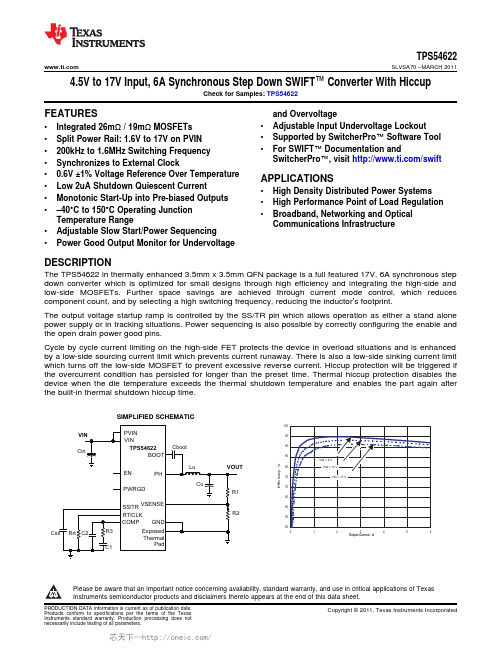
PRODUCTION DATA information is current as of publication date. Products conform to specifications per the terms of the Texas Instruments standard warranty. Production processing does not necessarily include testing of all parameters.
WHITE SPACE
SIMPLIFIED SCHEMATIC
VIN Cin
Css Rrt C2
PVIN VIN
TPS54622
BOOT
Cboot
EN
PH
PWRGD
Lo Co
SS/TR VSENSE RT/CLK COMP GND
al
C1
Pad
VOUT R1 R2
Efficiency - %
Temperature Range • Adjustable Slow Start/Power Sequencing • Power Good Output Monitor for Undervoltage
and Overvoltage • Adjustable Input Undervoltage Lockout • Supported by SwitcherPro™ Software Tool • For SWIFT™ Documentation and
Cycle by cycle current limiting on the high-side FET protects the device in overload situations and is enhanced by a low-side sourcing current limit which prevents current runaway. There is also a low-side sinking current limit which turns off the low-side MOSFET to prevent excessive reverse current. Hiccup protection will be triggered if the overcurrent condition has persisted for longer than the preset time. Thermal hiccup protection disables the device when the die temperature exceeds the thermal shutdown temperature and enables the part again after the built-in thermal shutdown hiccup time.
Agilent 54600系列振幅比例器探头与配件选择指南数据表说明书

Agilent Technologies 54600-SeriesOscilloscope Probes and AccessoriesSelection Guide Data Sheet. . . . . . . . . . . . . . . 12. . . . . . . . . . . . . . . . . . . . 14. . . . . . . . . . . . . . . 14GPIB. . . . . . . . . . . . . . . . . . . . . . . . . . . . . . . . . . 15. . . . . . . . . . . . . . . . . . . . . . . . . . . . . . . . 15. . . . . . . . . 15Testmobile. . . . . . . . . . . . . . . . . . . . . . . . . . . . . 15. . . . . . . . . . . . . . . . . . . . . . . . . . 15Rackmount Kit. . . . . . . . . . . . . . . . . . . . . . . . . . 15. . . 16Probe Compatibility TableFor ordering information when replacing your probe or probe accessory:Refer directly to the page number listed in the table of contents for your probe model.To assist you in selectingthe proper probe for your application: Use our probe compatibility table below to find the probes that are recommended for use with your 54600-Series oscilloscope.23•Designed for optimal performance with your Agilent 54600-Series scope•1:1 and 10:1 attenuation •20 to 500 MHzRugged, high-quality probes at a reasonable priceAgilent 10070-family passiveprobes are a great choice if you’re looking for high quality at a very reasonable price. These general-purpose probes are designed specifically to give you optimal performance with your 54600-Series oscilloscopes.Ruggedized for general-purpose measurements, they feature adurable cable and a solid stainless steel probe body encased with a hard, fracture-resistant plastic.They’re designed and tested to ensure the probes operate in the toughest of conditions.Passive Probes10074C Passive Probe4High-voltage Passive Probes10076A Passive ProbeN2771A High-voltage Probe10076A Derating CurveN2771A Derating Curve5Differential ProbesDerating of each input for the N2772AN2772 20 MHz Differential Probe 1141A 200 MHz Differential Probe6Active Probes1144A Active Probe 1145A Active Probe7Mixed Signal Oscilloscope Logic Probes54620-68701 Logic Probe10085-68701 Logic ProbeTermination adapter included in the 10085-687018Current Probes•Choice of dc-100 kHz and dc-50 MHz bandwidth•Hybrid technology to measure ac and dc•Compatible with any 1 M Ωscope input Accurate current measurements without breaking the circuitCompatible with any scope or voltage measuring instruments with BNC input, the 1146A and N2774A offer accurate and reli-able solutions for measuring dc and ac currents. The probes use a hybrid technology that includes a Hall effect sensor, which senses the dc current and a current transformer, which senses the ac current, making it unnecessary to make an electrical connection to the circuit.N2774A 50 MHz current probe andN2775A power supply1146A 100 kHz Current Probe The 1146A ac/dc current probe provides accurate display and measurement of currents from 100 mA to 100 Arms, dc to 100kHz, without breaking into the circuit. A battery level indica-tor and overload indicator help ensure proper readings. It con-nects directly to the scopethrough a 2 m coaxial cable with an insulated BNC.N2774A 50 MHz Current Probe The N2774A is a high bandwidth,active current probe, featuring flat bandwidth (dc-50 MHz), low noise (<2.5 mArms) and low cir-cuit insertion loss. In conjunction with the power supply (model N2775A), this probe can be used with any oscilloscope having a BNC input. The companion power supply N2775A (2x 12 Vdc output) lets you connect twoN2774As to a single power supply.1146A 100 kHz current probe9Current Probes (continued)10Agilent Wedge Probe Adapter•Easy connection to surface mount ICs•Safe, with no chance of shorting •Mechanically non-invasive contact •3-, 8-, and 16-signal versions •Supports 0.5 mm and 0.65mm TQFP and PQFP packages Problem-free probingThe Agilent Wedge Probe Adapter eliminates many of the frustra-tions associated with probing surface mount components. If you’ve ever accidentally shorted IC pins together, experienced electrical and/or mechanical problems with soldering small wires onto leads, or gotten frus-trated juggling multiple probes while you’re trying to operate your scope, the Wedge was designed with you in mind.Make the inaccessible accessible When you use the Wedge, you don’t have to worry about short-ing IC pins together on a delicate component — or worse yet on an irreplaceable prototype. The Wedge is easy to insert and it stays put. There’s no need to solder small wires onto leads. The Wedge is mechanically non-invasive, so you won’t damage the legs of the IC. Instead, you’ll have easy access to hard-to-reach components.Electrical reliabilityThe Wedge makes two contact points with each leg of the IC.This redundant physical connec-tion increases the electricalreliability of the connection. And the Wedge’s low capacitance and inductance provides superior performance to many other alternatives.Printer Kit•Easily print screens and setups •No separate power supply requiredEverything you need for easy and portable documentationThe Agilent N2727A printer kit comes complete with everything you need for easy documentation directly from your 54600-Series scope. It lets you easily print screen displays and key setup parameters so you can include them in reports and share them with colleagues.You don’t need a separate power supply with this thermal printer because it’s powered directly from your oscilloscope. And it includes a specially designed short, flat, parallel cable to make it easy to connect to your scope. Store the printer in the special pouch that fits on top of your scope – it includes a separate compartment where you can conveniently store your probes and accessories, too. It comes with three rolls of printer paper –enough for you to print 200 screen captures with setup information.11CAN Trigger Module •Trigger on CAN 2.0A/B message frames with user specified IDsand/or data•Trigger on Error frames •Differential CAN •Acknowledge On/Off•Built In QuickHelp•Remote Control via GPIB/RS232•Compatible with 54621D, 54622D, 54641D, 54642DThe N2758A CAN trigger module extends your Mixed Signal Oscilloscope’s (MSO) capabilities beyond the standard CAN SOF trigger. The module enables theMSO to isolate and trigger on a particular frame’s content. This triggering allows you to:•sort through frame traffic on the bus•isolate frames of interest •specify particular frame characteristics•trigger and measure latency between CAN frames meetingthe user specificationThe CAN trigger module is ideal for analyzing all traffic on the broadcast network. Quickly find frames that meet the specifica-tions you select with an isolating capability similar to pattern triggering across multiple chan-nels in the parallel domain. Synchronize to the particular frame then examine the system behavior of interest.The N2758A kit includes the CAN trigger module, digital cable, ten grabbers, andtwo probe ground leads.Use the N2758A CAN trigger module with the54621D, 54622D, 54641D, 54642D Mixed SignalOscilloscopes (MSOs) for quick and easy triggering.1213CAN Trigger Module (continued)The N2758A CAN trigger module reduces the time required to debug your mixed signal CAN based designs.The N2758A CAN trigger module makes it easy to sort through frame traffic and isolate a specific frame.14PC Connectivity•Ideal for documentation and archiving•Works in familiar Microsoft ®Excel and Word environments•Leverage the power of Excel for data analysis and advanced graphing•ActiveX controls provided for more flexible scope programming •It’s included standard!Get scope data into your PC without programming with Agilent IntuiLink To simplify the task of transfer-ring images and waveform data to your PC, Agilent IntuiLink2.187510010002.187510010002.2510010002.187500010002.18750001000200010002.062500010001.87500010001.87500010001.87511110001.7511100001.87511100001.687511100001.687511100001.687501100001.562501100001.562501100001.501100001.501100001.437510100001.37510100001.2510100001.2510100001.187510100001.187500100001.12500100001.06251Simple transfer of images and data with IntuiLinksoftware is included free with 100MHz, 350MHz, and 500MHz 54600-Series scopes. IntuiLink provides easy access to the scope data and images from within your standard PC applications. You work in a familiar environment at all times, using PC applications such as Microsoft Excel or Word to analyze, interpret, display,print, and document the data you get from the scope. The IntuiLink application toolbar makes it easy,providing a simple way to down-load data and screenshots into a spreadsheet or document. You can also save the scope settings and retrieve them later to repro-Agilent 82341C Agilent 82341DHigh-performance Plug&play, high-performance duce difficult setups like glitch capture and complex triggering.Programmers can use an ActiveX control to program instruments directly using high-level toolbar functions. With IntuiLink, pro-grammers also have access to the scope’s SCPI commands to tackle complex tasks. IntuiLink brings the barriers down, simplifying the way you do your job.If you choose one of the 60 MHz 54600-Series scopes, you can download free Agilent IntuiLink software available at/find/intuilink15PC Connectivity (continued)GPIB for fast data transfers If you need fast data transfers,equip your 54600-Series scope with GPIB communication.Agilent offers a GPIB card for your PC, as well as a cable, and a GPIB I/O communication module that provides a GPIB port for your scope.RS-232 cableIf you need an RS-232 cable for your 60MHz 54620-Series scope,order the Agilent 34398A RS-232cable. It comes standard with 100MHz, 350MHz, and 500MHz models.Miscellaneous AccessoriesCarrying CaseThe Agilent 1185A Carrying Case makes transporting and shipping your 54600-Series oscilloscope safe and simple. A scope, optional module and other accessories fit neatly inside the padded shell of hard plastic and the case is lock-able for shipment.Agilent Technologies ’ Test and Measurement Support, Services, and AssistanceAgilent Technologies aims to maximize the value you receive, while minimizing your risk and problems. We strive to ensure that you get the test and measurement capabilities you paid for and obtain the support you need. Our extensive support resources and services can help you choose the right Agilent products for your applications and apply them successfully.Every instrument and system we sell has a global warranty. Support is available for at least five years beyond the production life of the product. Two concepts underlie Agilent's overall support policy: "Our Promise" and "Your Advantage."Our PromiseOur Promise means your Agilent test and measurement equipment will meet its advertised performance and functionality. When you are choosing new equipment, we will help you with product information, including realistic performance specifications and practical recommendations from experienced test engineers. When you use Agilent equipment, we can verify that it works properly, help with product operation, and provide basic measurement assistance for the use of specified capabilities, at no extra cost upon request. Many self-help tools are available.Your AdvantageYour Advantage means that Agilent offers a wide range of additional expert test and measurement services, which you can purchase according to your unique technical and business needs. Solve problems efficiently and gain a competitive edge by contracting with us for calibration, extra-cost upgrades, out-of-warranty repairs, and on-site education and training, as well as design, system integration, project management, and other professional engineering services. Experienced Agilent engineers and technicians worldwide can help you maximize your productivity, optimize the return on investment of your Agilentinstruments and systems, and obtain dependable measurement accuracy for the life of those products.By internet, phone, or fax, get assistance with all your test & measurement needs Online assistance:/find/assist Phone or Fax United States:(tel) 800 452 4844Canada:(tel) 877 894 4414(fax) 905 282 6495China:(tel) 800 810 0189(fax) 800 820 2816Europe:(tel) (31 20) 547 2323(fax) (31 20) 547 2390Japan:(tel) (81) 426 56 7832(fax) (81) 426 56 7840Korea:(tel) (82 2) 2004 5004(fax) (82 2) 2004 5115Latin America:(tel) (305) 269 7500(fax) (305) 269 7599Taiwan:(tel) 0800 047 866(fax) 0800 286 331Other Asia Pacific Countries:(tel) (65) 6375 8100(fax) (65) 6836 0252Email:*******************Product specifications and descriptions in this document subject to change without notice.© Agilent Technologies, Inc. 2003Printed in USA February 10, 20035968-8153ENMICROSOFT, WINDOWS, WINDOWS NT, VISUAL STUDIO .NET, VISUAL BASIC and the VISUAL BASIC Logo areregistered trademarks of Microsoft Corporation in the U.S. and/or other countries./find/emailupdatesGet the latest information on the products and applications you select.Agilent T&M Software and ConnectivityAgilent's Test and Measurement software and connectivity products, solutions and developer network allows you to take time out of connecting your instruments to your computer with tools based on PC standards, so you can focus on your tasks, not on your connections. Visit /find/connectivity for more information.。
IC datasheet pdf-ULQ2003A-Q1,ULQ2004A-Q1,pdf(High-Voltage High-Current Darlington Transistor Array)
D OR PW PACKAGE(TOP VIEW)1B 1162B 2153B 3144B 4135B 5126B 6117B 710E891C 2C 3C 4C 5C 6C 7C COMULQ2003A-Q1ULQ2004A-Q1SGLS148D –DECEMBER 2002–REVISED APRIL 2010HIGH-VOLTAGE HIGH-CURRENT DARLINGTON TRANSISTOR ARRAYSCheck for Samples:ULQ2003A-Q1,ULQ2004A-Q1FEATURES•Qualified for Automotive Applications•ESD Protection Exceeds 200V Using Machine Model (C =200pF,R =0)•500-mA-Rated Collector Current (Single Output)•High-Voltage Outputs:50V •Output Clamp Diodes•Inputs Compatible With Various Types of Logic•Relay-Driver ApplicationsDESCRIPTIONThe ULQ2003A and ULQ2004A are high-voltage high-current Darlington transistor arrays.Each consists of seven npn Darlington pairs that feature high-voltage outputs with common-cathode clamp diodes for switching inductive loads.The collector-current rating of a single Darlington pair is 500mA.The Darlington pairs can be paralleled for higher current capability.Applications include relay drivers,hammer drivers,lamp drivers,display drivers (LED and gas discharge),line drivers,and logic buffers.The ULQ2003A has a 2.7-k Ωseries base resistor for each Darlington pair,for operation directly with TTL or 5-V CMOS devices.The ULQ2004A has a 10.5-k Ωseries base resistor to allow operation directly from CMOS devices that use supply voltages of 6V to 15V.The required input current of the ULQ2004A is below that of the ULQ2003A.ORDERING INFORMATION (1)T APACKAGE (2)ORDERABLE PART NUMBER TOP-SIDE MARKING Tube of 40ULQ2003ATDQ1ULQ2003AT Reel of 2500ULQ2003ATDRQ1SOIC –D–40°C to 105°CTube of 40ULQ2004ATDQ1Product Preview Reel of 2500ULQ2004ATDRQ1ULQ2004AT TSSOP –PWReel of 2000ULQ2003ATPWRQ1U2003AT –40°C to 125°C SOIC –DReel of 2500ULQ2003AQDRQ1ULQ2003AQ(1)For the most current package and ordering information,see the Package Option Addendum at the end of this document,or see the TI web site at .(2)Package drawings,thermal data,and symbolization are available at /packaging .Please be aware that an important notice concerning availability,standard warranty,and use in critical applications of Texas Instruments semiconductor products and disclaimers thereto appears at the end of this data sheet.7C 6C 5C 4C 3C 2C 1CCOM7B6B5B4B3B2B1BULQ2003A:R = 2.7 k B W ULQ2004A:R = 10.5 k B ULQ2003A-Q1ULQ2004A-Q1SGLS148D –DECEMBER 2002–REVISED APRIL 2010LOGIC DIAGRAMSCHEMATICS (EACH DARLINGTON PAIR)A.All resistor values shown are nominal.B.The collector-emitter diode is a parasitic structure and should not be used to conduct current.If the collector(s)go below ground an external Schottky diode should be added to clamp negative undershoots.2Submit Documentation Feedback Copyright ©2002–2010,Texas Instruments IncorporatedULQ2003A-Q1ULQ2004A-Q1 SGLS148D–DECEMBER2002–REVISED APRIL2010 ABSOLUTE MAXIMUM RATINGS(1)at25°C free-air temperature(unless otherwise noted)MIN MAX UNITV CC Collector-emitter voltage50V Clamp diode reverse voltage(2)50VV I Input voltage(2)30V Peak collector current See Figure14500mAI OK Output clamp current500mATotal emitter-terminal current–2.5ASee DissipationP D Continuous total power dissipationRatings TableULQ200xAT–40105T A Operating free-air temperature range°CULQ200xAQ–40125D package73q JA Package thermal impedance(3)(4)°C/WPW package108T stg Storage temperature range–65150°C (1)Stresses beyond those listed under"absolute maximum ratings"may cause permanent damage to the device.These are stress ratingsonly,and functional operation of the device at these or any other conditions beyond those indicated under"recommended operating conditions"is not implied.Exposure to absolute-maximum-rated conditions for extended periods may affect device reliability.(2)All voltage values are with respect to the emitter/substrate terminal E,unless otherwise noted.(3)Maximum power dissipation is a function of T J(max),q JA,and T A.The maximum allowable power dissipation at any allowable ambienttemperature is P D=(T J(max)–T A)/q JA.Operating at the absolute maximum T J of150°C can affect reliability.(4)The package thermal impedance is calculated in accordance with JESD51-7.DISSIPATION RATINGSDERATINGT A=25°CFACTOR T A=85°C T A=105°C T A=125°C PACKAGE POWERABOVE POWER RATING POWER RATING POWER RATINGRATINGT A=25°CD950mW7.6mW/°C494mW342mW190mW Copyright©2002–2010,Texas Instruments Incorporated Submit Documentation Feedback3ULQ2003A-Q1ULQ2004A-Q1SGLS148D –DECEMBER 2002–REVISED APRIL 2010ELECTRICAL CHARACTERISTICSover recommended operating conditions (unless otherwise noted)ULQ2003AT ULQ2003AQ ULQ2004AT TEST PARAMETERTEST CONDITIONSUNITFIGUREMINTYP MAXMINTYP MAXMINTYP MAXI C =125mA 5I C =200mA2.7 2.76I C =250mA 2.92.9On-state input V I(on)Figure 6V CE =2VV voltageI C =275mA 7I C =300mA 33I C =350mA8I I =250m A,I C =100mA 0.9 1.21 1.30.9 1.1Collector-emitter V CE(sat)saturation Figure 5I I =350m A,I C =200mA 1 1.41 1.51 1.3VvoltageI I =500m A,I C =350mA1.21.7 1.21.8 1.21.6T A =25°C 10010050V CE =50V,Figure 1I I =0T A =105°C 165Collector cutoff I CEXm A currentI I =0100Figure 2V CE =50V V I =1V500Clamp forward V F Figure 8I F =350mA1.72.21.72.21.72.1V voltage Off-state input I I(off)Figure 3V CE =50V,I C =500m A 306530655065m Acurrent V I =3.85V0.931.350.931.35I IInput current Figure 4V I =5V 0.350.5mAV I =12V11.45T A =25°C10010050Clamp reverse I R Figure 7V R =50V m A current 100100100InputC iV I =0,f =1MHz152515251525pF capacitanceSWITCHING CHARACTERISTICSover recommended operating conditions (unless otherwise noted)ULQ2003A,ULQ2004APARAMETERTEST CONDITIONSUNIT MINTYP MAX t PLH Propagation delay time,low-to high-level output See Figure 9110m s t PHL Propagation delay time,high-to low-level output See Figure 9110m s V S –V OHHigh-level output voltage after switchingV S =50V,I O =300mA,See Figure 10mV5004Submit Documentation Feedback Copyright ©2002–2010,Texas Instruments IncorporatedOpenOpenOpenV IOpenOpenVIOpenI COpenI CI IOpenI CIFV RULQ2003A-Q1ULQ2004A-Q1SGLS148D –DECEMBER 2002–REVISED APRIL 2010PARAMETER MEASUREMENT INFORMATIONFigure 1.I CEX Test CircuitFigure 2.I CEX Test CircuitFigure 3.I I(off)Test CircuitFigure 4.I I Test CircuitC.I I is fixed for measuring V CE(sat),variable for measuring h FE .Figure 5.h FE ,V CE(sat)Test CircuitFigure 6.V I(on)Test CircuitFigure 7.I R Test Circuit Figure 8.V F Test CircuitFigure 9.Propagation Delay-Time WaveformsCopyright ©2002–2010,Texas Instruments Incorporated Submit Documentation Feedback 5V IH(see Note C)0V V OHV OLOutputVOLTAGEWAVEFORMSULQ2003A-Q1ULQ2004A-Q1SGLS148D –DECEMBER 2002–REVISED APRIL 2010PARAMETER MEASUREMENT INFORMATION (continued)A.The pulse generator has the following characteristics:PRR =12.5kHz,Z O =50Ω.B.C L includes probe and jig capacitance.C.For testing the ULQ2003A,V IH =3V;for the ULQ2004A,V IH =8V.Figure tch-Up Test Circuit and Voltage Waveforms6Submit Documentation Feedback Copyright ©2002–2010,Texas Instruments Incorporated0I C -Collector Current -mA 2.58001002003004005006007000.511.52V C E (s a t )-C o l l e c t o r -E m i t t e r S a t u r a t i o n V o l t a g e -V V C E (s a t )21.510.570060050040030020010008002.5I C(tot)-Total Collector Current -mA0V CE (s a t )-C o l l e c t o r -E m i t t e r S a t u r a t i o n V o l t a g e -VC E (s a t )0I I -Input Current -µA500200025507510012515017550100150200250300350400450I C -C o l l e c t o r C u r r e n t -m AC 0Duty Cycle -%6001000102030405060708090100200300400500C -M a x i m u m C o l l e c t o r C u r r e n t -m AC I ULQ2003A-Q1ULQ2004A-Q1SGLS148D –DECEMBER 2002–REVISED APRIL 2010TYPICAL CHARACTERISTICSCOLLECTOR-EMITTER SATURATION VOLTAGECOLLECTOR-EMITTER SATURATION VOLTAGEvsvsTOTAL COLLECTOR CURRENT (TWO DARLINGTONS INCOLLECTOR CURRENT (ONE DARLINGTON)PARALLEL)Figure 11.Figure 12.D PACKAGECOLLECTOR CURRENTMAXIMUM COLLECTOR CURRENTvsvsINPUT CURRENTDUTY CYCLEFigure 13.Figure 14.Copyright ©2002–2010,Texas Instruments Incorporated Submit Documentation Feedback 7VVULQ2004A ULQ2003ALam TestV VV VULQ2003A-Q1ULQ2004A-Q1SGLS148D –DECEMBER 2002–REVISED APRIL 2010APPLICATION INFORMATIONFigure 15.TTL to LoadFigure 16.Buffer for Higher Current LoadsFigure e of Pullup Resistors to Increase Drive Current8Submit Documentation Feedback Copyright ©2002–2010,Texas Instruments IncorporatedPACKAGING INFORMATIONOrderable Device Status(1)PackageType PackageDrawingPins PackageQtyEco Plan(2)Lead/Ball Finish MSL Peak Temp(3)ULQ2003AQDRQ1ACTIVE SOIC D162500Green(RoHS&no Sb/Br)CU NIPDAU Level-1-260C-UNLIMULQ2003ATDG4Q1ACTIVE SOIC D1640Green(RoHS&no Sb/Br)CU NIPDAU Level-1-260C-UNLIMULQ2003ATDQ1ACTIVE SOIC D1640Green(RoHS&no Sb/Br)CU NIPDAU Level-1-260C-UNLIMULQ2003ATDRG4Q1ACTIVE SOIC D162500Green(RoHS&no Sb/Br)CU NIPDAU Level-1-260C-UNLIMULQ2003ATDRQ1ACTIVE SOIC D162500Green(RoHS&no Sb/Br)CU NIPDAU Level-1-260C-UNLIMULQ2003ATPWRQ1ACTIVE TSSOP PW162500Green(RoHS&no Sb/Br)CU NIPDAU Level-1-260C-UNLIMULQ2004ATDRG4Q1ACTIVE SOIC D162500Green(RoHS&no Sb/Br)CU NIPDAU Level-1-260C-UNLIMULQ2004ATDRQ1ACTIVE SOIC D162500Green(RoHS&no Sb/Br)CU NIPDAU Level-1-260C-UNLIM(1)The marketing status values are defined as follows:ACTIVE:Product device recommended for new designs.LIFEBUY:TI has announced that the device will be discontinued,and a lifetime-buy period is in effect.NRND:Not recommended for new designs.Device is in production to support existing customers,but TI does not recommend using this part in a new design.PREVIEW:Device has been announced but is not in production.Samples may or may not be available.OBSOLETE:TI has discontinued the production of the device.(2)Eco Plan-The planned eco-friendly classification:Pb-Free(RoHS),Pb-Free(RoHS Exempt),or Green(RoHS&no Sb/Br)-please check /productcontent for the latest availability information and additional product content details.TBD:The Pb-Free/Green conversion plan has not been defined.Pb-Free(RoHS):TI's terms"Lead-Free"or"Pb-Free"mean semiconductor products that are compatible with the current RoHS requirements for all6substances,including the requirement that lead not exceed0.1%by weight in homogeneous materials.Where designed to be soldered at high temperatures,TI Pb-Free products are suitable for use in specified lead-free processes.Pb-Free(RoHS Exempt):This component has a RoHS exemption for either1)lead-based flip-chip solder bumps used between the die and package,or2)lead-based die adhesive used between the die and leadframe.The component is otherwise considered Pb-Free(RoHS compatible)as defined above.Green(RoHS&no Sb/Br):TI defines"Green"to mean Pb-Free(RoHS compatible),and free of Bromine(Br)and Antimony(Sb)based flame retardants(Br or Sb do not exceed0.1%by weight in homogeneous material)(3)MSL,Peak Temp.--The Moisture Sensitivity Level rating according to the JEDEC industry standard classifications,and peak solder temperature.Important Information and Disclaimer:The information provided on this page represents TI's knowledge and belief as of the date that it is provided.TI bases its knowledge and belief on information provided by third parties,and makes no representation or warranty as to the accuracy of such information.Efforts are underway to better integrate information from third parties.TI has taken and continues to take reasonable steps to provide representative and accurate information but may not have conducted destructive testing or chemical analysis on incoming materials and chemicals.TI and TI suppliers consider certain information to be proprietary,and thus CAS numbers and other limited information may not be available for release.In no event shall TI's liability arising out of such information exceed the total purchase price of the TI part(s)at issue in this document sold by TI to Customer on an annual basis.OTHER QUALIFIED VERSIONS OF ULQ2003A-Q1,ULQ2004A-Q1:•Catalog:ULQ2003A,ULQ2004ANOTE:Qualified Version Definitions:•Catalog-TI's standard catalog productTAPE AND REEL INFORMATION*All dimensions are nominal Device Package Type Package DrawingPinsSPQ Reel Diameter (mm)Reel Width W1(mm)A0(mm)B0(mm)K0(mm)P1(mm)W (mm)Pin1Quadrant ULQ2003ATPWRQ1TSSOP PW 162500330.012.4 6.9 5.6 1.68.012.0Q1*All dimensions are nominalDevice Package Type Package Drawing Pins SPQ Length(mm)Width(mm)Height(mm)ULQ2003ATPWRQ1TSSOP PW162500346.0346.029.0IMPORTANT NOTICETexas Instruments Incorporated and its subsidiaries(TI)reserve the right to make corrections,modifications,enhancements,improvements, and other changes to its products and services at any time and to discontinue any product or service without notice.Customers should obtain the latest relevant information before placing orders and should verify that such information is current and complete.All products are sold subject to TI’s terms and conditions of sale supplied at the time of order acknowledgment.TI warrants performance of its hardware products to the specifications applicable at the time of sale in accordance with TI’s standard warranty.Testing and other quality control techniques are used to the extent TI deems necessary to support this warranty.Except where mandated by government requirements,testing of all parameters of each product is not necessarily performed.TI assumes no liability for applications assistance or customer product design.Customers are responsible for their products and applications using TI components.To minimize the risks associated with customer products and applications,customers should provide adequate design and operating safeguards.TI does not warrant or represent that any license,either express or implied,is granted under any TI patent right,copyright,mask work right, or other TI intellectual property right relating to any combination,machine,or process in which TI products or services are rmation published by TI regarding third-party products or services does not constitute a license from TI to use such products or services or a warranty or endorsement e of such information may require a license from a third party under the patents or other intellectual property of the third party,or a license from TI under the patents or other intellectual property of TI.Reproduction of TI information in TI data books or data sheets is permissible only if reproduction is without alteration and is accompanied by all associated warranties,conditions,limitations,and notices.Reproduction of this information with alteration is an unfair and deceptive business practice.TI is not responsible or liable for such altered rmation of third parties may be subject to additional restrictions.Resale of TI products or services with statements different from or beyond the parameters stated by TI for that product or service voids all express and any implied warranties for the associated TI product or service and is an unfair and deceptive business practice.TI is not responsible or liable for any such statements.TI products are not authorized for use in safety-critical applications(such as life support)where a failure of the TI product would reasonably be expected to cause severe personal injury or death,unless officers of the parties have executed an agreement specifically governing such use.Buyers represent that they have all necessary expertise in the safety and regulatory ramifications of their applications,and acknowledge and agree that they are solely responsible for all legal,regulatory and safety-related requirements concerning their products and any use of TI products in such safety-critical applications,notwithstanding any applications-related information or support that may be provided by TI.Further,Buyers must fully indemnify TI and its representatives against any damages arising out of the use of TI products in such safety-critical applications.TI products are neither designed nor intended for use in military/aerospace applications or environments unless the TI products are specifically designated by TI as military-grade or"enhanced plastic."Only products designated by TI as military-grade meet military specifications.Buyers acknowledge and agree that any such use of TI products which TI has not designated as military-grade is solely at the Buyer's risk,and that they are solely responsible for compliance with all legal and regulatory requirements in connection with such use. TI products are neither designed nor intended for use in automotive applications or environments unless the specific TI products are designated by TI as compliant with ISO/TS16949requirements.Buyers acknowledge and agree that,if they use any non-designated products in automotive applications,TI will not be responsible for any failure to meet such requirements.Following are URLs where you can obtain information on other Texas Instruments products and application solutions:Products ApplicationsAmplifiers Audio /audioData Converters Automotive /automotiveDLP®Products Communications and /communicationsTelecomDSP Computers and /computersPeripheralsClocks and Timers /clocks Consumer Electronics /consumer-appsInterface Energy /energyLogic Industrial /industrialPower Mgmt Medical /medicalMicrocontrollers Security /securityRFID Space,Avionics&/space-avionics-defenseDefenseRF/IF and ZigBee®Solutions /lprf Video and Imaging /videoWireless /wireless-appsMailing Address:Texas Instruments,Post Office Box655303,Dallas,Texas75265Copyright©2010,Texas Instruments Incorporated。
IC datasheet pdf-24LCS22A pdf datasheet
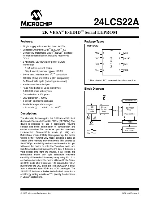
—
400
4.5V ≤ VCC ≤ 5.5V
2
THIGH
Clock high time
4000 600
—
ns 2.5V ≤ VCC ≤ 5.5V
—
4.5V ≤ VCC ≤ 5.5V
3Leabharlann TLOWClock low time
4700 1300
—
ns 2.5V ≤ VCC ≤ 5.5V
—
4.5V ≤ VCC ≤ 5.5V
for monitor identification, including recovery to DDC1
• 2 Kbit Serial EEPROM Low-power CMOS technology:
- 1 mA active current, typical - 10 μA standby current, typical at 5.5V • 2-wire serial interface bus, I2C™ compatible
—
V VCC ≥ 2.7V (Note)
D4
VIL
Low-level input voltage
—
0.2 VCC V VCC ≤ 2.7V (Note)
D5
VHYS
Hysteresis of Schmitt Trigger .05 VCC
—
Inputs
V (Note)
D6
VOL1
Low-level output voltage
TABLE 1-1: DC CHARACTERISTICS
DC CHARACTERISTICS
Vcc = +2.5V to 5.5V Industrial (I): TA = -40°C to +85°C
CS5462-IS资料
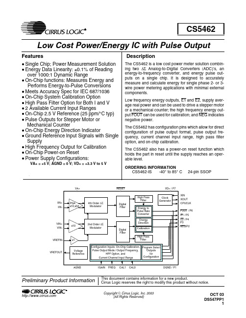
Configuration Inputs: On-Chip Calibration, Program Select Outputs Pulse Output Mode / Output Frequency, for HPF Option, and Configuration Current Channel Input Range
Energy to Pulse Rate Converter Energy Direction
VIN+ VIN-
x10
2nd Order ∆Σ Modulator
Digital Filter
Calibration High Pass Filter
VREFIN
x1
VREFOUT
Voltage Reference
AGND
IGAIN
FREQ
CAL1
CAL0
DGND / P1
Preliminary Product Information
t contains information for a new product. Cirrus Logic reserves the right to modify this product without notice.
VA+ = +5 V; AGND = 0 V; VD+ = +3.3 V to 5 V
Description
The CS5462 is a low cost power meter solution combining two ∆Σ Analog-to-Digital Converters (ADC)’s, an energy-to-frequency converter, and energy pulse outputs on a single chip. It is designed to accurately measure and calculate energy for single phase 2- or 3wire power metering applications with minimal external components. Low frequency energy outputs, E1 and E2, supply average real power and can be used to drive a stepper motor or a mechanical counter; the high frequency energy output FOUT can be used for calibration; and NEG indicates negative power. The CS5462 has configuration pins which allow for direct configuration of pulse output format, pulse output frequency, current channel input range, high pass filter option, and on-chip calibration. The CS5462 also has a power-on reset function which holds the part in reset until the supply reaches an operable level. ORDERING INFORMATION CS5462-IS -40° to 85° C 24-pin SSOP
CS5464电能计量芯片 中文版
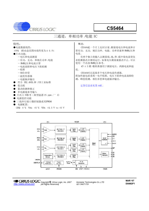
概述:
CS5464是一个片上瓦时计量。测量线电压和电流和计 算有功,无功,视在功率,电能,功率因素和RMS电压和 电流。
有两个独立的输入去测量线,地,和/或中线电流使仪 表检测篡改并继续运行。如果电压测量被篡改中止,可以 使用一个内部RMS电压参考。
4个ΔΣ模-数转换器用于测量电压,两路电流和温 度。
CS5464可以连接多个电压和电流传感器, 附加性能包括系统-电平校准,电压下跌和电流故障检 测,峰值检测,相位补偿和电能脉冲输出。
定货信息请见第44页。
Copyright © Cirrus Logic, Inc. 2007
(All Rights Reserved)
5.1.2 电流1和电流2输入 ................................................................17 5.1.3 功率故障监控输入 ................................................................17
2
DS682F1
5.1.4 参考电压输入 .............................................1.5 参考电压输出 ....................................................................17
Honestar Technologies Co.,LTD 021-54071701
MAR ‘07 DS682F1
CS5464
目录
1.综述 .................................................................
IC9642芯片说明书
DATASHEET12-Ch a n n e l1:2M UX/DE M UX IC9642 Revision V0.1COPYRIGHT©2020 Shenzhen IcSpring Technology Co., Ltd all rights reserved. No part of this document may be reproduced, transmitted, transcribed, stored in a retrieval system, or translated into any language in any form or by any means without the written permission of Shenzhen IcSpring Technology Co., Ltd.DISCLAIMERIcSpring Technology Co. Ltd provides this document “as is”, without warranty of any kind, neither expressed nor implied, including, but not limited to, the particular purpose. IcSpring Technology Co. reserves the right to make changes at any time without notice to improve and supply the best possible product and is not responsible and does not assume any liability for misapplication or use outside the limits specified in this document. This document could include technical inaccuracies or typographical errors.TRADEMARKSIcSpring is a trademark, of Shenzhen IcSpring Technology Co., Ltd. Other names mentioned in this document trademarks/registered trademarks of their respective owners.USING THIS DOCUMENTThis document is intended for the hardware and software engineer’s general information on the IcSpring IC9642 12-Channel 1:2 MUX/DEMUX IC.Though every effort has been made to ensure that this document is current and accurate, more information may have become available subsequent to the production of this guide. In that event, please contact your IcSpring representative for additional information that may help in the development process.REVISION HISTORYTable of Contents1. Introduction (4)1.1 Description (4)2. Features (5)2.1 General System Features (5)2.2 Applications (5)3. Pin Assignment (6)3.1 Pin Assignment Diagram (6)3.2 Pin Descriptions (7)4. System Architecture and Reference Design (9)4.1 Functional Block Diagram (9)4.2 Device Functional Modes (9)4.3 HDMI Application Schematic (10)5. Electrical Characteristics (11)5.1 Absolute Maximum Ratings (11)5.2 DC Characteristics (11)5.3 Switching Characteristics (12)5.4 HDMI Eye Pattern (12)6. Mechanical Information (13)7. Application Circuits (14)7.1 Circuit (15)7.2 Layout Guidelines (15)7.3 Layout Example (16)1.Introduction1.1 DescriptionThe IC9642 is a 12 channel 1:2 or 2:1 bidirectional multiplexer/demultiplexer. The IC9642 operates 3.3V and offers low resistance to achieve a typical bandwidth of up to 6.9 GHz. The device provides the high bandwidth necessary for HDMI 2.0 applications. The IC9642 offers a power down mode to operate minimal power consumption.2.Features2.1. General System Features• 2:1 multiplexer• 1:2 demultiplexer• VCC: 3.3V• I/O: 0 ~ 5V• Support HDMI 2.0 up to 4K 60Hz• ESD Performance– 2KV Human Body Model• 42-pin WQFN Package (9 mm x 3.5 mm, 0.5 mm pitch)2.2 Applications• General Purpose DVI 1.0•DisplayPort•TMDS•LVDS•High-Speed•HDMI Signal Switching3. Pin Assignment3.1 Pin AssignmentFigure 3.1 Pin Assignment Diagram3.2 Pin Descriptions4. System Functional Descriptions 4.1 Functional Block DiagramFigure 4.1IC9642 Block Diagram4.2 Device Functional ModesFigure 4.2 Functional Table4.3 HDMI Application Schematic5. Electrical Characteristics5.1 Absolute Maximum RatingsTable 5.1. Absolute Maximum Ratings5.2 DC CharacteristicsTable 5.2 General DC Characteristics6. Mechanical InformationFigure 6.1 Mechanical Information Diagram。
- 1、下载文档前请自行甄别文档内容的完整性,平台不提供额外的编辑、内容补充、找答案等附加服务。
- 2、"仅部分预览"的文档,不可在线预览部分如存在完整性等问题,可反馈申请退款(可完整预览的文档不适用该条件!)。
- 3、如文档侵犯您的权益,请联系客服反馈,我们会尽快为您处理(人工客服工作时间:9:00-18:30)。
• High speed, 1.4GHz product available (EL5167 & EL5167)
• High speed, 4mA, 630MHz product available (EL5164 & EL5165)
CAUTION: Stresses above those listed in “Absolute Maximum Ratings” may cause permanent damage to the device. This is a stress only rating and operation of the device at these or any other conditions above those indicated in the operational sections of this specification is not implied.
-1
0.22
+1
µA/V
+IIN
+ Input Current
-IIN
- Input Current
RIN
Input Resistance
CIN
Input Capacitance
OUTPUT CHARACTERISTICS
-8
0.5
+8
µA
-10
2
+10
µA
0.8
1.6
3
MΩ
1
pF
VO IOUT
Output Voltage Swing Output Current
kΩ
CMIR
Common Mode Input Range
Guaranteed by CMRR test
±3
±3.3
V
CMRR -ICMR
Common Mode Rejection Ratio
VIN = ±3V
- Input Current Common Mode Rejection
50
62
75
dB
CONDITIONS
MIN TYP MAX UNIT
AC PERFORMANCE
BW BW1
-3dB Bandwidth 0.1dB Bandwidth
AV = +1, RL = 500Ω, RF = 598Ω AV = +2, RL = 150Ω, RF = 422Ω
500
MHz
233
MHz
30
MHz
Supply Voltage between VS+ and VS- . . . . . . . . . . . . . . . . . . . 13.2V Maximum Continuous Output Current . . . . . . . . . . . . . . . . . . . 50mA Maximum Voltage between IN+ and IN-, Disabled . . . . . . . . . ±1.5V Current into IN+, IN-, CE . . . . . . . . . . . . . . . . . . . . . . . . . . . . . ±5mA Slew Rate from VS+ to VS- . . . . . . . . . . . . . . . . . . . . . . . . . . . 1V/µs
IMPORTANT NOTE: All parameters having Min/Max specifications are guaranteed. Typical values are for information purposes only. Unless otherwise noted, all tests are at the specified temperature and are pulsed tests, therefore: TJ = TC = TA
specified. (Continued)
PARAMETER
Copyright © Intersil Americas Inc. 2005. All Rights Reserved.
All other trademarks mentioned are the property of their respective owners.
EL5462
Absolute Maximum Ratings (TA = 25°C)
Electrical Specifications VS+ = +5V, VS- = -5V, RF = 750Ω for AV = 1, RF = 400Ω for AV = 2, RL = 150Ω, TA = 25°C unless otherwise
specified.
PARAMETER
DESCRIPTION
RL = 150Ω to GND RL = 1kΩ to GND RL = 10Ω to GND
±3.35 ±3.6 ±3.75
V
±3.75 ±3.9 ±4.15
V
60
100
mA
2
FN7492.0
February 14, 2005
EL5462ຫໍສະໝຸດ Electrical Specifications VS+ = +5V, VS- = -5V, RF = 750Ω for AV = 1, RF = 400Ω for AV = 2, RL = 150Ω, TA = 25°C unless otherwise
®
Data Sheet
February 14, 2005
EL5462
FN7492.0
500MHz Low Power Current Feedback Amplifier
The EL5462 is a current feedback amplifier with a bandwidth of 500MHz which makes this amplifier ideal for today’s high speed video and monitor applications.
The EL5462 is available in a 14-pin SO package and operates over the industrial temperature range of -40°C to +85°C.
Pinout
EL5462 (14-PIN SO) TOP VIEW
OUTA 1 INA- 2 INA+ 3
14-Pin SO
-
MDP0027
(See Note)
(Pb-Free)
EL5462ISZ-T7
14-Pin SO
7”
MDP0027
(See Note)
(Pb-Free)
EL5462ISZ-T13 14-Pin SO
13”
MDP0027
(See Note)
(Pb-Free)
NOTE: Intersil Pb-free products employ special Pb-free material sets; molding compounds/die attach materials and 100% matte tin plate termination finish, which are RoHS compliant and compatible with both SnPb and Pb-free soldering operations. Intersil Pb-free products are MSL classified at Pb-free peak reflow temperatures that meet or exceed the Pb-free requirements of IPC/JEDEC J STD-020.
Ordering Information
PART NUMBER PACKAGE
TAPE & REEL
PKG. DWG. #
EL5462IS
14-Pin SO
-
MDP0027
EL5462IS-T7
14-Pin SO
7”
MDP0027
EL5462IS-T13
14-Pin SO
13”
MDP0027
EL5462ISZ
14 OUTD
A -+
D +-
13 IND-
12 IND+
VS+ 4
11 VS-
INB+ 5 INB- 6 OUTB 7
10 INC+
-+ +BC
9 INC8 OUTC
Features
• 500MHz -3dB bandwidth
• 4000V/µs slew rate
• 1.5mA supply current per amplifier
SR
Slew Rate
tS
0.1% Settling Time
eN
Input Voltage Noise
iN-
IN- Input Current Noise
iN+
IN+ Input Current Noise
dG
Differential Gain Error (Note 1)
dP
Differential Phase Error (Note 1)