Slanted-Edge_MTF_Stability_Repeatability
CS42L51中文资料

Advance Product InformationThis document contains information for a new product.Cirrus Logic reserves the right to modify this product without notice.Low Power, Stereo CODEC with Headphone AmpDIGITAL to ANALOG FEATURES!98 dB Dynamic Range (A-wtd) !-86 dB THD+N!Headphone Amplifier - GND Centered–On-Chip Charge Pump Provides -VA_HP –No DC-Blocking Capacitor Required –46mW Power Into Stereo 16Ω @ 1.8V –88mW Power Into Stereo 16Ω @ 2.5V –-75 dB THD+N!Digital Signal Processing Engine–Bass & Treble Tone Control, De-Emphasis –PCM + ADC Mix w/Independent Vol Control –Master Digital Volume Control–Soft Ramp & Zero Cross Transitions ! Beep Generator–Tone Selections Across Two Octaves –Separate Volume Control–Programmable On & Off Time Intervals –Continuous, Periodic or One-Shot Beep Selections!Programmable Peak-Detect and Limiter !Pop and Click SuppressionANALOG to DIGITAL FEATURES!98 dB Dynamic Range (A-wtd)! -88 dB THD+N !Analog Gain Controls–+32 dB or +16 dB MIC Pre-Amplifiers –Analog Programmable Gain Amplifier (PGA)!+20 dB Digital Boost!Programmable Automatic Level Control (ALC)–Noise Gate for Noise Suppression –Programmable Threshold and Attack/Release Rates!Independent Channel Control !Digital Volume Control!High-Pass Filter Disable for DC Measurements !Stereo 3:1 Analog Input MUX !Dual MIC Inputs–Programmable, Low Noise MIC Bias Levels –Differential MIC Mix for Common Mode Noise Rejection!Very Low 64 Fs Oversampling Clock ReducesPower ConsumptionCS42L51SYSTEM FEATURES!24-bit Converters! 4 kHz to 96kHz Sample Rate!Multi-bit Delta Sigma Architecture!Low Power Operation–Stereo Playback: 12.93 mW @ 1.8 V–Stereo Record and Playback: 20.18 mW @1.8 V!Variable Power Supplies– 1.8 V to 2.5 V Digital & Analog– 1.8 V to 3.3V Interface Logic!Power Down Management–ADC, DAC, CODEC, MIC Pre-Amplifier, PGA!Software Mode (I²C & SPI™ Control)!Hardware Mode (Stand-Alone Control)!Digital Routing/Mixes:–Analog Out=ADC+Digital In–Digital Out=ADC+Digital In–Internal Digital Loopback–Mono Mixes!Flexible Clocking Options–Master or Slave Operation–High-Impedance Digital Output Option (for easy MUXing between CODEC and OtherData Sources)–Quarter-Speed Mode - (i.e. Allows 8 kHz Fs while maintaining a flat noise floor up to16kHz)APPLICATIONS!HDD & Flash-Based Portable Audio Players !MD Players/Recorders!PDAs!Personal Media Players!Portable Game Consoles!Digital Voice Recorders!Digital Camcorders!Digital Cameras!Smart Phones GENERAL DESCRIPTIONThe CS42L51 is a highly integrated, 24-bit, 96kHz, low power stereo CODEC. Based on multi-bit, delta-sigma modulation, it allows infinite sample rate adjustment be-tween 4 kHz and 96 kHz. Both the ADC and DAC offer many features suitable for low power, portable system applications.The ADC input path allows independent channel control of a number of features. An input multiplexer selects be-tween line-level or microphone level inputs for each channel. The microphone input path includes a select-able programmable-gain pre-amplifier stage and a low noise MIC bias voltage supply. A PGA is available for line or microphone inputs and provides analog gain with soft ramp and zero cross transitions. The ADC also fea-tures a digital volume attenuator with soft ramp transitions. A programmable ALC and Noise Gate mon-itor the input signals and adjust the volume levels appropriately.The DAC output path includes a digital signal process-ing engine. Tone Control provides bass and treble adjustment of four selectable corner frequencies. The Mixer allows independent volume control for both the ADC mix and the PCM mix, as well as a master digital volume control for the analog output. All volume level changes may be configured to occur on soft ramp and zero cross transitions. The DAC also includes de-em-phasis, limiting functions and a beep generator delivering tones selectable across a range of two full octaves.The stereo headphone amplifier is powered from a sep-arate positive supply and the integrated charge pump provides a negative supply. This allows a ground-cen-tered analog output with a wide signal swing and eliminates external DC-blocking capacitors.In addition to its many features, the CS42L51 operates from a low-voltage analog and digital core, making this CODEC ideal for portable systems that require ex-tremely low power consumption in a minimal amount of space.The CS42L51 is available in a 32-pin QFN package in both Commercial (-10 to +70° C) and Automotive grades (-40 to +85° C). The CDB42L51 Customer Dem-onstration board is also available for device evaluation and implementation suggestions. Please see “Ordering Information” on page81 for complete details.TABLE OF CONTENTS1. PIN DESCRIPTIONS - SOFTWARE (HARDWARE) MODE (7)1.1 Digital I/O Pin Characteristics (9)2. TYPICAL CONNECTION DIAGRAMS (10)3. CHARACTERISTIC AND SPECIFICATION TABLES (12)SPECIFIED OPERATING CONDITIONS (12)ABSOLUTE MAXIMUM RATINGS (12)ANALOG INPUT CHARACTERISTICS (COMMERCIAL - CNZ) (13)ANALOG INPUT CHARACTERISTICS (AUTOMOTIVE - DNZ) (14)ADC DIGITAL FILTER CHARACTERISTICS (15)ANALOG OUTPUT CHARACTERISTICS (COMMERCIAL - CNZ) (16)ANALOG OUTPUT CHARACTERISTICS (AUTOMOTIVE - DNZ) (17)LINE OUTPUT VOLTAGE CHARACTERISTICS (18)HEADPHONE OUTPUT POWER CHARACTERISTICS (19)COMBINED DAC INTERPOLATION & ON-CHIP ANALOG FILTER RESPONSE (20)SWITCHING SPECIFICATIONS - SERIAL PORT (20)SWITCHING SPECIFICATIONS - I²C CONTROL PORT (22)SWITCHING CHARACTERISTICS - SPI CONTROL PORT (23)DC ELECTRICAL CHARACTERISTICS (24)DIGITAL INTERFACE SPECIFICATIONS & CHARACTERISTICS (24)POWER CONSUMPTION (25)4. APPLICATIONS (26)4.1 Overview (26)4.1.1 Architecture (26)4.1.2 Line & MIC Inputs (26)4.1.3 Line & Headphone Outputs (26)4.1.4 Signal Processing Engine (26)4.1.5 Beep Generator (26)4.1.6 Device Control (Hardware or Software Mode) (26)4.1.7 Power Management (26)4.2 Hardware Mode (27)4.3 Analog Inputs (28)4.3.1 Digital Code, Offset & DC Measurement (28)4.3.2 High-Pass Filter and DC Offset Calibration (29)4.3.3 Digital Routing (29)4.3.4 Differential Inputs (29)4.3.4.1 External Passive Components (29)4.3.5 Analog Input Multiplexer (30)4.3.6 MIC & PGA Gain (31)4.3.7 Automatic Level Control (ALC) (31)4.3.8 Noise Gate (32)4.4 Analog Outputs (33)4.4.1 De-Emphasis Filter (33)4.4.2 Volume Controls (34)4.4.3 Mono Channel Mixer (34)4.4.4 Beep Generator (34)4.4.5 Tone Control (35)4.4.6 Limiter (35)4.4.7 Line-Level Outputs and Filtering (36)4.4.8 On-Chip Charge Pump (36)4.5 Serial Port Clocking (37)4.5.1 Slave (37)4.5.2 Master (38)4.5.3 High-Impedance Digital Output (38)4.5.4 Quarter- and Half-Speed Mode (39)4.6 Digital Interface Formats (39)4.7 Initialization (40)4.8 Recommended Power-Up Sequence (40)4.9 Recommended Power-Down Sequence (41)4.10 Software Mode (42)4.10.1 SPI Control (42)4.10.2 I²C Control (42)4.10.3 Memory Address Pointer (MAP) (44)4.10.3.1 Map Increment (INCR) (44)5. REGISTER QUICK REFERENCE (45)6. REGISTER DESCRIPTION (47)6.1 Chip I.D. and Revision Register (Address 01h) (Read Only) (47)6.2 Power Control 1 (Address 02h) (47)6.3 MIC Power Control & Speed Control (Address 03h) (48)6.4 Interface Control (Address 04h) (49)6.5 MIC Control (Address 05h) (51)6.6 ADC Control (Address 06h) (52)6.7 ADCx Input Select, Invert & Mute (Address 07h) (53)6.8 DAC Output Control (Address 08h) (54)6.9 DAC Control (Address 09h) (55)6.10 ALCX & PGAX Control:ALCA, PGAA (Address 0Ah) & ALCB, PGAB (Address 0Bh) (56)6.11 ADCx Attenuator:ADCA (Address 0Ch) & ADCB (Address 0Dh) (57)6.12 ADCx Mixer Volume Control:ADCA (Address 0Eh) & ADCB (Address 0Fh) (58)6.13 PCMX Mixer Volume Control:PCMA (Address 10h) & PCMB (Address 11h) (59)6.14 Beep Frequency & Timing Configuration (Address 12h) (60)6.15 Beep Off Time & Volume (Address 13h) (61)6.16 Beep Configuration & Tone Configuration (Address 14h) (62)6.17 Tone Control (Address 15h) (63)6.18 AOUTx Volume Control:AOUTA (Address 16h) & AOUTB (Address 17h) (64)6.20 Limiter Threshold SZC Disable (Address 19h) (65)6.21 Limiter Release Rate Register (Address 1Ah) (66)6.22 Limiter Attack Rate Register (Address 1Bh) (67)6.23 ALC Enable & Attack Rate (Address 1Ch) (67)6.24 ALC Release Rate (Address 1Dh) (68)6.25 ALC Threshold (Address 1Eh) (69)6.26 Noise Gate Configuration & Misc. (Address 1Fh) (70)6.27 Status (Address 20h) (Read Only) (71)6.28 Charge Pump Frequency (Address 21h) (71)7. ANALOG PERFORMANCE PLOTS (72)7.1 Headphone THD+N versus Output Power Plots (72)7.2 ADC_FILT+ Capacitor Effects on THD+N (74)8. EXAMPLE SYSTEM CLOCK FREQUENCIES (75)8.1 Auto Detect Enabled (75)8.2 Auto Detect Disabled (76)9. PCB LAYOUT CONSIDERATIONS (77)9.1 Power Supply, Grounding (77)9.2 QFN Thermal Pad (77)10. ADC & DAC DIGITAL FILTERS (78)11. PARAMETER DEFINITIONS (79)12. PACKAGE DIMENSIONS (80)THERMAL CHARACTERISTICS (80)13. ORDERING INFORMATION (81)14. REFERENCES (81)15. REVISION HISTORY (82)LIST OF FIGURESFigure 1. Typical Connection Diagram (Software Mode) (10)Figure 2. Typical Connection Diagram (Hardware Mode) (11)Figure 3. Headphone Output Test Load (19)Figure 4. Serial Audio Interface Slave Mode Timing (21)Figure 5. TDM Serial Audio Interface Timing (21)Figure 6. Serial Audio Interface Master Mode Timing (21)Figure 7. Control Port Timing - I²C (22)Figure 8. Control Port Timing - SPI Format (23)Figure 9. Analog Input Architecture (28)Figure 10. MIC Input Mix w/Common Mode Rejection (30)Figure 11. Differential Input (30)Figure 12. ALC (31)Figure 13. Noise Gate Attenuation (32)Figure 14. Output Architecture (33)Figure 15. De-Emphasis Curve (33)Figure 16. Beep Configuration Options (34)Figure 17. Peak Detect & Limiter (35)Figure 18. Master Mode Timing (38)Figure 19. Tri-State Serial Port (38)Figure 20. I²S Format (39)Figure 21. Left-Justified Format (39)Figure 22. Right-Justified Format (DAC only) (39)Figure 23. Initialization Flow Chart (41)Figure 24. Control Port Timing in SPI Mode (42)Figure 25. Control Port Timing, I²C Write (43)Figure 26. Control Port Timing, I²C Read (43)Figure 27. AIN & PGA Selection (53)Figure 28. THD+N vs. Ouput Power per Channel at 1.8V (16 Ω load) (72)Figure 29. THD+N vs. Ouput Power per Channel at 2.5V (16 Ω load) (72)Figure 30. THD+N vs. Ouput Power per Channel at 1.8V (32 Ω load) (73)Figure 31. THD+N vs. Ouput Power per Channel at 2.5V (32 Ω load) (73)Figure 32. ADC THD+N vs. Frequency w/Capacitor Effects (74)Figure 33. ADC Passband Ripple (78)Figure 34. ADC Stopband Rejection (78)Figure 35. DAC Passband Ripple (78)Figure 36. DAC Stopband (78)Figure 35. DAC Transition Band (78)Figure 36. DAC Transition Band (Detail) (78)Figure 35. ADC Transition Band (78)Figure 36. ADC Transition Band (Detail) (78)1.PIN DESCRIPTIONS - SOFTWARE (HARDWARE) MODEPin Name#Pin DescriptionLRCK 1Left Right Clock (Input/Output ) - Determines which channel, Left or Right, is currently active on the serial audio data line.SDA/CDIN 2Serial Control Data (Input /Output ) - SDA is a data I/O in I²C mode. CDIN is the input data line for the control port interface in SPI mode.(MCLKDIV2)MCLK Divide by 2 (Input ) - Hardware Mode: Divides the MCLK by 2 prior to all internal circuitry.SCL/CCLK 3Serial Control Port Clock (Input ) - Serial clock for the serial control port.(I²S/LJ)Interface Format Selection (Input ) - Hardware Mode: Selects between I²S & Left-Justified interface for-mats for the ADC & DAC.AD0/CS 4Address Bit 0 (I²C) / Control Port Chip Select (SPI) (Input) - AD0 is a chip address pin in I²C mode; CS is the chip select signal for SPI format.(DEM)De-Emphasis (Input) - Hardware Mode: Enables/disables the de-emphasis filter.VA_HP 5Analog Power For Headphone (Input) - Positive power for the internal analog headphone section.FLYP 6Charge Pump Cap Positive Node (Input) - Positive node for the external charge pump capacitor.GNDHP 7Analog Ground (Input ) - Ground reference for the internal headphone/charge pump section.FLYN 8Charge Pump Cap Negative Node (Input) - Negative node for the external charge pump capacitor.VSS_HP 9Negative Voltage From Charge Pump (Output) - Negative voltage rail for the internal analog head-phone section.AOUTB AOUTA 1011Analog Audio Output (Output ) - The full-scale output level is specified in the DAC Analog Characteris-tics specification table.VA 12Analog Power (Input) - Positive power for the internal analog section.AGND13Analog Ground (Input) - Ground reference for the internal analog section.M /S )V S S _H A O U T BA O U T V A G N D A C _F I L T A D C _F I L T VDAC_FILT+ ADC_FILT+1416Positive Voltage Reference (Output) - Positive reference voltage for the internal sampling circuits.VQ15Quiescent Voltage (Output) - Filter connection for internal quiescent voltage.MICIN1/ AIN3A 17Microphone Input 1 (Input) - The full-scale level is specified in the ADC Analog Characteristics specifi-cation table.MICIN2/ BIAS/AIN3B 18Microphone Input 2 (Input/Output) - The full-scale level is specified in the ADC Analog Characteristics specification table. This pin can also be configured as an output to provide a low noise bias supply for an external microphone. Electrical characteristics are specified in the DC Electrical Characteristics table.AIN2A19Analog Input (Input) - The full-scale level is specified in the ADC Analog Characteristics specification table.AIN2B/BIAS20Analog Input (Input/Output) - The full-scale level is specified in the ADC Analog Characteristics specifi-cation table. This pin can also be configured as an output to provide a low noise bias supply for an exter-nal microphone. Electrical characteristics are specified in the DC Electrical Characteristics table.AFILTA AFILTB 2122Filter Connection (Output) - Filter connection for the ADC inputs.AIN1A AIN1B 2324Analog Input (Input) - The full-scale level is specified in the ADC Analog Characteristics specification table.RESET25Reset (Input) - The device enters a low power mode when this pin is driven low.VL26Digital Interface Power (Input) - Determines the required signal level for the serial audio interface and host control port. Refer to the Recommended Operating Conditions for appropriate voltages.VD27Digital Power (Input) - Positive power for the internal digital section.DGND28Digital Ground (Input) - Ground reference for the internal digital section.SDOUT29Serial Audio Data Output (Output) - Output for two’s complement serial audio data.(M/S)Serial Port Master/Slave (Input/Output) - Hardware Mode Startup Option: Selects between master and slave mode for the serial port.MCLK30Master Clock (Input) -Clock source for the delta-sigma modulators.SCLK31Serial Clock (Input/Output) - Serial clock for the serial audio interface.SDIN32Serial Audio Data Input (Input) - Input for two’s complement serial audio data.Thermal Pad-Thermal relief pad for optimized heat dissipation. See “QFN Thermal Pad” on page77.1.1Digital I/O Pin CharacteristicsThe logic level for each input should adhere to the corresponding power rail and should not exceed the maximum ratings.Power Rail Pin NameSW/(HW)I/O Driver ReceiverVL RESET Input- 1.8 V - 3.3 V SCL/CCLK(I²S/LJ)Input- 1.8 V - 3.3 V, with HysteresisSDA/CDIN(MCLKDIV2)Input/Output 1.8 V - 3.3 V, CMOS/Open Drain 1.8 V - 3.3 V, with HysteresisAD0/CS(DEM)Input- 1.8 V - 3.3 V MCLK Input- 1.8 V - 3.3 VLRCK Input/Output 1.8 V - 3.3 V, CMOS 1.8 V - 3.3 VSCLK Input/Output 1.8 V - 3.3 V, CMOS 1.8 V - 3.3 VSDOUT(M/S)Input/Output 1.8 V - 3.3 V, CMOS 1.8 V - 3.3 V SDIN Input- 1.8 V - 3.3 VTable 1. I/O Power Rails2.TYPICAL CONNECTION DIAGRAMSFigure 1. Typical Connection Diagram (Software Mode)Figure 2. Typical Connection Diagram (Hardware Mode)3.CHARACTERISTIC AND SPECIFICATION TABLES(All Min/Max characteristics and specifications are guaranteed over the Specified Operating Conditions. Typical performance characteristics and specifications are derived from measurements taken at nominal supply voltages and T A = 25° C.)SPECIFIED OPERATING CONDITIONS(AGND=DGND=0 V, all voltages with respect to ground.)ABSOLUTE MAXIMUM RATINGS(AGND = DGND = 0 V; all voltages with respect to ground.)WARNING:Operation at or beyond these limits may result in permanent damage to the device. Normal operationis not guaranteed at these extremes.Notes:1.The device will operate properly over the full range of the analog, headphone amplifier, digital core andserial/control port interface supplies.2.Any pin except supplies. Transient currents of up to ±100 mA on the analog input pins will not causeSCR latch-up.3.The maximum over/under voltage is limited by the input current.ParametersSymbol Min NomMaxUnitsDC Power Supply (Note 1)Analog Core VA 1.712.37 1.82.5 1.892.63V V Headphone Amplifier VA_HP 1.712.37 1.82.5 1.892.63V V Digital CoreVD 1.712.37 1.82.5 1.892.63V V Serial/Control Port InterfaceVL1.712.373.14 1.82.53.3 1.892.633.47V V V Ambient TemperatureCommercial - CNZ Automotive - DNZT A-10-40--+70+85°C °CParametersSymbol MinMaxUnitsDC Power SupplyAnalog Digital Serial/Control Port Interface VA, VA_HP VDVL-0.3-0.3-0.3 3.03.04.0V V V Input Current(Note 2)I in -±10mAAnalog Input Voltage(Note 3)V INAGND-0.7VA+0.7VDigital Input Voltage (Note 3))V IND-0.3VL+ 0.4V Ambient Operating Temperature Commercial - CNZ(power applied)Automotive - DNZT A -20-50+85+95°C °C Storage TemperatureT stg-65+150°C(Test Conditions (unless otherwise specified): All supplies = VA = 2.5 V and 1.8 V; Input sine wave (relative to dig-ital full-scale): 1kHz through passive input filter; Measurement Bandwidth is 10Hz to 20kHz unless otherwise specified. Sample Frequency = 48kHz)VA = 2.5V VA = 1.8VParameter (Note 4)Min Typ Max Min Typ Max Unit Analog In to ADC (PGA bypassed)Dynamic Range A-weightedunweighted 93909996--90879693--dBdBTotal Harmonic Distortion + Noise -1dBFS-20dBFS-60dBFS ----86-76-36-80------84-73-33-78--dBdBdBAnalog In to PGA to ADC Dynamic RangePGA Setting: 0 dB A-weightedunweighted 92899895--89869592--dBdBPGA Setting: +12 dB A-weightedunweighted 85829188--82798885--dBdBTotal Harmonic Distortion + NoisePGA Setting: 0 dB -1dBFS -60dBFS ---88-35-82----86-32-80-dBdBPGA Setting: +12 dB -1dBFS--85-79--83-77dB Analog In to MIC Pre-Amp(+16 dB) to PGA to ADCDynamic RangePGA Setting: 0 dB A-weightedunweighted --8683----8380--dBdBTotal Harmonic Distortion + NoisePGA Setting: 0 dB -1dBFS--76---74-dB Analog In to MIC Pre-Amp(+32 dB) to PGA to ADCDynamic RangePGA Setting: 0 dB A-weightedunweighted --7874----7571--dBdBTotal Harmonic Distortion + NoisePGA Setting: 0 dB -1dBFS--74---71-dB Other CharacteristicsDC AccuracyInterchannel Gain Mismatch-0.1--0.1-dB Gain Drift-±100--±100-ppm/°C InputInterchannel Isolation-90--90-dB DAC Isolation (Note 5)-70--70-dB Full-scale Input Voltage (x•VA) (Note 7)0.70•VA0.72•VA0.75•VA0.70•VA0.72•VA0.75•VA VppInput Impedance (Note 6)ADCPGAMIC 184050------184050------kΩkΩkΩ(Test Conditions (unless otherwise specified): All supplies = VA = 2.5 V and 1.8 V; Input sine wave (relative to full-scale): 1 kHz through passive input filter; Measurement Bandwidth is 10Hz to 20kHz unless otherwise specified. Sample Frequency = 48kHz)Notes:4.Referred to the typical full-scale voltage.5.Measured with DAC delivering full-scale output power into 16 Ω.VA = 2.5V VA = 1.8V Parameter (Note 4)MinTypMaxMinTypMaxUnitAnalog In to ADCDynamic RangeA-weighted unweighted91789996--88859693--dB dB Total Harmonic Distortion + Noise -1dB -20dB-60dB ----86-76-36-78------84-73-33-76--dB dB dBAnalog In to PGA to ADC Dynamic RangePGA Setting: 0 dB A-weighted unweighted 90879895--87849592--dB dB PGA Setting: +12 dBA-weighted unweighted83809188--80778885--dB dB Total Harmonic Distortion + Noise PGA Setting: 0 dB -1dB -60dB ---88-35-80----86-32-78-dB dB PGA Setting: +12 dB -1dB--85-77--83-75dBAnalog In to MIC Pre-Amp (+16 dB) to PGA to ADC Dynamic RangePGA Setting: 0 dBA-weighted unweighted--8683----8380--dB dB Total Harmonic Distortion + Noise PGA Setting: 0 dB-1dB--76---74-dBAnalog In to MIC Pre-Amp (+32 dB) to PGA to ADC Dynamic RangePGA Setting: 0 dBA-weighted unweighted--7874----7571--dB dB Total Harmonic Distortion + Noise PGA Setting: 0 dB-1dB--74---71-dBOther CharacteristicsDC AccuracyInterchannel Gain Mismatch -0.1--0.1-dB Gain Drift-±100--±100-ppm/°C InputInterchannel Isolation -90--90-dB DAC Isolation (Note 5)-70--70-dB Full-scale Input Voltage (Note 7) 0.70•VA 0.72•VA0.75•VA0.70•VA 0.72•VA0.75•VAVpp Input Impedance (Note 6)ADC PGA MIC 184050------184050------k Ωk Ωk ΩNotes:6.Measured between AINxx and AGND.7.Full-scale input voltage characteristics for the PGA and Microphone inputs are scaled based on the gainsetting for each.ADC DIGITAL FILTER CHARACTERISTICSNotes:8.Response is clock dependent and will scale with Fs. Note that the response plots (Figures 33to 36 onpage 78) have been normalized to Fs and can be de-normalized by multiplying the X-axis scale by Fs.Parameter (Note 8)MinTypMaxUnitPassband (Frequency Response) to -0.1 dB corner0-0.4948Fs Passband Ripple -0.09-0dB Stopband0.6677--Fs Stopband Attenuation 48.4--dB Total Group Delay-2.7/Fs -s High-Pass Filter CharacteristicsFrequency Response -3.0 dB -0.13 dB -- 3.724.2--Hz Hz Phase Deviation @ 20Hz-10-Deg Passband Ripple --0.17dB Filter Settling Time-105/Fss(Test conditions (unless otherwise specified): Input test signal is a full-scale 997 Hz sine wave; measurement bandwidth is 10 Hz to 20 kHz; Sample Frequency = 48 kHz; test load R L = 10 kΩ, C L = 10 pF for the line output (see Figure3), and test load R L = 16 Ω, C L = 10 pF (see Figure3) for the headphone output. HP_GAIN[2:0] = 011.)Parameter(Note 9)VA = 2.5VMin Typ MaxVA = 1.8VMin Typ Max UnitR L = 10 kΩDynamic Range18 to 24-Bit A-weighted unweighted 16-Bit A-weightedunweighted 9289--98959693----8986--95929390----dBdBdBdBTotal Harmonic Distortion + Noise18 to 24-Bit0 dB-20 dB-60 dB 16-Bit0 dB-20 dB-60 dB -------86-75-35-86-73-33-80------------88-72-32-88-70-30-82-----dBdBdBdBdBdBR L = 16 ΩDynamic Range18 to 24-Bit A-weightedunweighted 16-Bit A-weightedunweighted 9289--98959693----8986--95929390----dBdBdBdBTotal Harmonic Distortion + Noise18 to 24-Bit0 dB-20 dB-60 dB 16-Bit0 dB-20 dB-60 dB -------75-75-35-75-73-33-69------------75-72-32-75-70-30-69-----dBdBdBdBdBdBOther Characteristics for R L = 16 Ω or 10 kΩOutput Parameters Modulation Index (MI) (Note 10)Analog Gain Multiplier (G)-0.67870.6047--0.67870.6047-Full-scale Output Voltage (2•G•MI•VA) (Note 10)Refer to Table“Line Output Voltage Characteristics” onpage18VppFull-scale Output Power (Note 10)Refer to Table“Headphone Output Power Characteristics” onpage19Interchannel Isolation (1 kHz)16 Ω10 kΩ--8095----8093--dBdBInterchannel Gain Mismatch-0.10.25-0.10.25dB Gain Drift-±100--±100-ppm/°C AC-Load Resistance (R L)(Note 11)16--16--ΩLoad Capacitance (C L)(Note 11)--150--150pF(Test conditions (unless otherwise specified): Input test signal is a full-scale 997 Hz sine wave; measurement bandwidth is 10 Hz to 20 kHz; Sample Frequency = 48 kHz and 96 kHz; test load R L = 10 kΩ, C L = 10 pF for the line output (see Figure3), and test load R L = 16 Ω, C L = 10 pF (see Figure3) for the headphone output.HP_GAIN[2:0] = 011.)Parameter(Note 9)VA = 2.5VMin Typ MaxVA = 1.8VMin Typ Max UnitR L = 10 kΩDynamic Range18 to 24-Bit A-weighted unweighted 16-Bit A-weightedunweighted 9087--98959693----8784--95929390----dBdBdBdBTotal Harmonic Distortion + Noise18 to 24-Bit0 dB-20 dB-60 dB 16-Bit0 dB-20 dB-60 dB -------86-75-35-86-73-33-78------------88-72-32-88-70-30-80-----dBdBdBdBdBdBR L = 16 ΩDynamic Range18 to 24-Bit A-weightedunweighted 16-Bit A-weightedunweighted 9087--98959693----8784--95929390----dBdBdBdBTotal Harmonic Distortion + Noise18 to 24-Bit0 dB-20 dB-60 dB 16-Bit0 dB-20 dB-60 dB -------75-75-35-75-73-33-67------------75-72-32-75-70-30-67-----dBdBdBdBdBdBOther Characteristics for R L = 16 Ω or 10 kΩOutput Parameters Modulation Index (MI) (Note 10)Analog Gain Multiplier (G)-0.67870.6047--0.67870.6047-Full-scale Output Voltage (2•G•MI•VA) (Note 10)Refer to Table “Line Output Voltage Characteristics” onpage18VppFull-scale Output Power (Note 10)Refer to Table “Headphone Output Power Characteristics” onpage19Interchannel Isolation (1 kHz)16 Ω10 kΩ--8095----8093--dBdBInterchannel Gain Mismatch-0.10.25-0.10.25dB Gain Drift-±100--±100-ppm/°C AC-Load Resistance (R L)(Note 11)16--16--ΩLoad Capacitance (C L)(Note 11)--150--150pF。
优化与防止被优化

注册登录•论坛•搜索•帮助•导航SoC Vista -- IC/FPGA设计家园» 30分钟必答 - 无限制提问专区» 设计未完成阶段进行面积评估如何防止被优化12下一页返回列表回复发帖mentor00超级通吃版主1#打印字体大小: t T发表于 2009-11-8 09:48 | 只看该作者设计未完成阶段进行面积评估如何防止被优化(本文来自anthonyyi的来信。
请大家一起来解答。
)为了对整个设计进行性能和面积的评估在模块尚未全部完成的阶段进入FPGA综合阶段在顶层设计中instance了所有已完成的模块但这些模块中有的由于后续模块没有完成,其输出悬空,即没有load在Synplify下使用Syn_noprune属性发现在compile阶段能保留上述模块,其RTL view显示模块存在在map之后观测Technology view发现上述模块已经被优化掉只剩下输入端口,且无drive故综合报告无实际意义和参考价值想请教在如何不改变顶层模块的输出管脚而使综合保留上述无输出的模块个人想到一种,用syn_probe将输出net probe出来,但这样会有风险因为综合工具似乎只会保留这些与该输出有关的逻辑而优化掉其他的部分而且该步骤没有进行实战确认:(本主题由 admin 于 2009-12-2 07:56 加入精华收藏分享评分回复引用订阅 TOPmentor00超级通吃版主2#发表于 2009-11-8 10:04 | 只看该作者我想可以参考一下下面的转载内容提问:我使用的是synplify pro综合verilog语言,例化了一个BUF,在综合结果里也看到了这个BUF,但是在MAP是这个BUF还是被优化掉了,请问用什么方法将这个BUF保留下来?解答:在这个BUF两端的信号线上加上下面的属性——wire bufin /* synthesis syn_keep=1 xc_props="X" */;wire bufout /* synthesis syn_keep=1 xc_props="X" */;解释下:1、syn_keep=1就是保留这个信号线,是它成为一个instance(synplify的),然后就可以对它添加XILINX的约束属性;2、xc_props=“”是synplify为XILINX保留留的约束属性,可以透传到ISE的实现中去,从而约束实现过程。
C28x_Fixed_Point_Library_v1_01

©Texas Instruments Inc., January 2011
v1.01
3
1. Introduction
The Texas Instruments TMS320C28x Fixed Point DSP Library is collection of highly optimized application functions written for the C28x. These functions enable C/C++ programmers to take full advantage of the performance potential of the C28x. This document provides a description of each function included within the library.
C28x Fixed Point DSP Library
Module User’s Guide
C28x Foundation Software
柔性检查作用域套件-USB 产品说明书
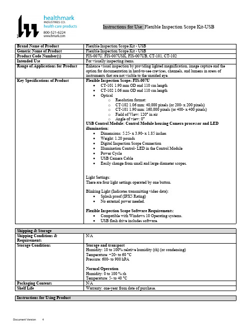
lInstructions for Use: Flexible Inspection Scope Kit-USB Brand Name of ProductFlexible Inspection Scope Kit - USB Generic Name of ProductFlexible Inspection Scope Kit - USB Product Code Number(s)FIS-007U, FIS-007USK, FIS-007UB, CT-101, CT-102Intended UseFor visually inspecting items.Range of Applications for ProductEnhance visual inspection by providing lighted magnification, image capture and the option for documentation in hard-to-see crevices, channels, and lumens in areas of instruments that are not visible to the unaided eye.Key Specifications of Product Flexible Inspection Scope- FIS-007U∙CT-101 1.90 mm OD and 110 cm length∙CT-102 1.06 mm OD and 110 cm length∙Opticalo Resolution format:o CT-102 1.06 mm: 40,000 pixels (or 200- x 200 pixels)o CT-101 1.90 mm: 160,000 pixels (or 400- x 400 pixels)o Field of View: 120° in airo Angle of view: 0°USB Control Module: Control Module housing Camera processor and LEDillumination:∙Dimensions: 5.25- x 3.90- x 1.85 inches∙Weight: 1.20 pounds ∙Digital Inspection Scope Connection∙Illumination Control- LED in the Control Module∙Power Cycle∙USB Camera Cable∙Easily change from small and large diameter scopes.Light Settings:There are four light settings operated by one button.Blinking Light (Indicates transmitting video data):∙Splash proof (IPX5 Rating)∙No external power needed.Flexible Inspection Scope Software Requirements:∙Compatible with Windows 10 Operating systems.∙USB flash drive includes software.Unpacking Flexible Inspection Scope:Carefully inspect for shipping damage. If there is any damage contact the shipping carrier and Heatlhmarkcustomer service 800-521-6224 immediately.USB Control Module: (Fig. 1).1.Digital Inspection Scope Connection 2.Illumination Control 3.Power Cycle B (Type C) on the right side of the boxFigure 1Flexible Inspection Scope™: (Fig. 2).∙CT-101 1.90 mm O.D. and 110 cm length ∙CT-102 1.06 mm O.D. and 110 cm lengthLarge1.90 mmSmall 1.06 mmFigure 2Flexible Inspection Scope™ Features3214Light/Illumination Settings: (Fig. 3).∙Five (5) light settingso Light on control indicats setting levelo Fifth setting is OFF∙Press light button to advance to next setting.∙Fifth setting turns the light OFF.Figure 3Power Cycle ButtonPress button to RESET camera (Fig. 4).Figure 41.Flexible Inspection Scope™ Plug (Fig. 5).Contains camera video connection as well as LED Light for illumination.1Figure 52.Flexible Working Length (Fig. 6).The portion of the Flexible Inspection Scope™ that is inserted into an item during visual inspection.The measuring scale markings on the Flexible Working Length are in centimeters (accuracy = ± 0.5 cm)2Figure 63.Distal Camera (Fig. 7).Distal portion of Flexible Inspection Scope™ that contains the camera lens3Figure 7SOFTWARE INSTALLATION:Note: This section is done only once when connecting the scope to the computer for the first time.∙System Requirements: MS Windows 10∙Install the Flexible Inspection Scope™ Software from the USB flash drive on a computer.Note: If you have any IT policies that may block this installation, please contact your IT team to give access to Healthmark scope viewer to install.1. Insert the USB Flash drive into your computer, and double click on the Healthmark Scope Viewer installer package to begin installation.2. The “Welcome to the Healthmark Scope Viewer Setup Wizard” screen pops up. Click on Next.3. Select the first tab Typical or setup type of your choice, click Next.4. Click Install and wait for installation to complete.5. Click Finish.STARTING SOFTWARE & CONNECTING SCOPE TO PC:(Fig 8).1.Open the Windows PC viewer software.2.Connect the Control Module to PC using USB Cable.3.Plug the Flexible Inspection Scope into the Control Module.4.In the viewer software, click Settings and Select USB Video Device, click on the desiredresolution, select the preferred Video Output Format, and then Click OK.5.Press the Power Cycle Button.Figure 86.Now you can start using the scope.Verifing OperationFollowing the steps listed below will ensure the proper use and performance of the Flexible Inspection Scope™. The Flexile Inspection Scope™ can be checked for normal operation by connecting it as described in the Startup section of this IFU.Normal operation includes:∙An image appearing on your computer monitor or HDMI Monitor.∙ A blinking light on Control Module near the Power Cycle button that indicates the image feed is transmitting.∙White light emitting from the distal end of the Digital Inspection Scope.∙An LED light on the control module top panel that indicates the light intensity of the device. Using SoftwareHealthmark Scope Viewer Software (Fig. 9).1.Capture button: Captures a Reference Image and saves it to the Reference Image folder.2.Main Image Window: Displays the image from the camera.3.Reference Image Window: Displays a reference image.4.Clear Button: Removes the image from the Reference image window.5.Open Reference Image button: Allows selection of a reference image from the Reference Imagefolder.6.Settings Button: Click to select the video camera and resolution settings.7.File Location Button: Click to change location where captured images are being saved.8.File Location Window: Shows the file path where captured images are being saved currently.9.Capture Image Button: Captures images and adds them to the File Location selected by the user(as shown in the File Location Window).10.Capture Video button: Click to record video. Click again to stop recording video.11.File Prefix: Type in text that you would like included in the file name of Captured Images.Figure 9Selecting Video Device or CameraFollow the directions below to select the video device or camera used to capture images using the Flexible Inspection Scope™ Viewer Software. (Fig. 10).1.Click Settings button in the lower left of the Scope Viewer software to display a list of videodevices or cameras being detected by your computer2.Select a device for capturing images using the Scope Viewera.The example below shows a webcam and USB Video Device in the Settings box. Select theUSB Video Device for the Flexible Inspection Scope™.b.You can also select your preferred Video Output Format from the dropdown box3.Click OK to view the selected Video Device.231Figure 10Capturing Still PicturesFollow the instructions for capturing still pictures from the Main Image Window.Select the Capture Image button. (Fig. 11).Figure 11Note: When an image is captured, “Image Captured” in red text will flash on the lower portion of the screen and a new file will appear in the Files Location.Capturing Video ImagesFollow the instructions below for capturing video from the Main Image Window.1.Select the Capture Video Button (Fig. 12).Figure 122.When the video is recording “Recording…” in red text will appear toward the bottom of thesoftware window.3.To stop recording, click Stop Capture. (Fig. 13).Figure 13Setting File PrefixFollowing the steps below allows you to create a file prefix that will appear after the underscore of image file names save to the File Location specified by the user.1.Click in the field next to File Prefix.2.Enter the characters that you would like to be included in the file name. (Fig 14).Figure 14Setting Location for Saved FilesFollowing the steps below allows you to set the file location of saved images using the Scope Viewer software.1.Click the File Location button.2.Select the file location you want to save captured images. (Fig 15).Figure 15Displaying Reference ImageThere are two ways to display a still image in the Reference Image Window on the Scope Viewer software.1.To display an image currently being displayed in the Main Image Window, click the Capture button. Note: The images will be saved in a file folder titled Reference Images in the designated File Location that the user specified in the File Location field. (Fig. 16).Figure 162.To display a saved image in the Reference Image Window from your File Location:a.Click the Open Reference Image button (Fig. 16 above).b.Select the file you want to display (Fig. 17 below).c.Click the OK Button, to display the image in the Reference Image Window. (Fig. 17).Figure 17Switching to a Different Flexible Inspection Scope™ on the Control Module:1.Press the Power button on the Control Module once.2.Disconnect the current Flexible Inspection Scope from the Control Module.3.Repeat the steps in the “STARTING SOFTWARE & CONNECTING SCOPE TO PC” procedure.Inserting Scope in ItemFigure 1Rotating Device to Avoid ObstacleFigure 2 Performing InspectionWipe down the Flexible Inspection Scope™ with a compatible wipe. Follow the manufacturer’s (Mfr.’s)Instructions for Use (IFU) for appropriate wipe usage. Click here to see the Chemical Compatibility Chart(PDF) for approved cleaning.The Flexible Inspection Scope™ is made of the same material as other common endoscopes. Any wipe,solution, or low temperature (≤ 60 °C [140 °F]) method intended for the reprocessing of endoscopes is likelycompatible with the Generation II Flexible Inspection Scope™ Catheters if used according to the productlabeling.Solutions Containing (Flexible Inspection Scope Only)Alcohol Ethoxylates Neutral or Near-Neutral pH DetergentsEnzymatic Cleaning Solutions Enzymatic DetergentsSodium Borated, Decahydrate Tetrapotassium PyrophosphateFlexible Inspection Scope™ has a fluid ingress protection rating of IPX7 (Waterproof) and can withstandimmersion in fluid up to one (1)-meter in depth for up to 30 minutes.Control Module USB has a fluid ingress protection rating of IPX5 (Water resistant) and can withstand asustained, low pressure water jet spray for up to three minutes.For Thorough Cleaning: CablesFollow the cleaning agent Mfr.’s IFU.1.Unplug and disconnect all components from the Control box prior to cleaning.2.Do not submerge or soak the cable for disinfection (cable is not waterproof).3.Wipe thoroughly with non-linting wipe moistened with facility approved neutral detergent. Use theappropriate brushes with detergent solution to remove any residues from areas that cannot bereached with the wipes.For Thorough Cleaning: Control Module1.Unplug and disconnect all components from the Control box prior to cleaning.2.Do not submerge or soak the cable for disinfection (Control Box is not waterproof).3.Wipe thoroughly with non-linting wipe moistened with facility approved neutral detergent. Use theappropriate brushes with detergent solution to remove any residues from areas that cannot bereached with the wipes.Note: Do NOT soak. Control Module and cables are not waterproof and should not be immersed.N/ACleaning –AutomatedDisinfection Control Module and CablesThese may be cleaned with alcohol based disinfectant wipes.Compatible agents (wipes and solutions) for disinfecting Flexible Inspection Scope™ and ControlModule:∙Hydrogen peroxide∙Isopropyl alcohol (IPA)∙Sodium hypochlorite (Bleach)∙Ortho-phenylphenol∙Quaternary ammonium.High-Level Disinfection (Flexible Inspection Scope™ Only)∙Select only disinfecting solutions listed in the compatible disinfecting methods.∙Follow all recommendations regarding health-hazards, dispensing, measuring, and storage from the Mfr. of cleaning and disinfecting agents.∙Soak the Flexible Inspection Scope™ in selected disinfecting solution per Mfr.’s IFU.∙Rinse the Flexible Inspection Scope™ with critical (sterile) water, again, following the disinfecting solutions Mfr.’s instructions.Reprocessing Chemical Compatibility Chart (PDF): Click here.。
AT28HC64B高性能电擦可编程只读存储器(EEPROM)说明书

Features Array•Fast Read Access Time – 70 ns•Automatic Page Write Operation–Internal Address and Data Latches for 64 Bytes•Fast Write Cycle Times–Page Write Cycle Time: 10 ms Maximum (Standard)2 ms Maximum (Option – Ref. AT28HC64BF Datasheet)–1 to 64-byte Page Write Operation•Low Power Dissipation–40 mA Active Current–100µA CMOS Standby Current•Hardware and Software Data Protection•DATA Polling and Toggle Bit for End of Write Detection•High Reliability CMOS Technology–Endurance: 100,000 Cycles–Data Retention: 10 Years•Single 5 V ±10% Supply•CMOS and TTL Compatible Inputs and Outputs•JEDEC Approved Byte-wide Pinout•Industrial Temperature Ranges•Green (Pb/Halide-free) Packaging Option Only1.DescriptionThe AT28HC64B is a high-performance electrically-erasable and programmable read-only memory (EEPROM). Its 64K of memory is organized as 8,192 words by 8 bits. Manufactured with Atmel’s advanced nonvolatile CMOS technology, the device offers access times to 55 ns with power dissipation of just 220 mW. When the device is deselected, the CMOS standby current is less than 100µA.The AT28HC64B is accessed like a Static RAM for the read or write cycle without the need for external components. The device contains a 64-byte page register to allow writing of up to 64 bytes simultaneously. During a write cycle, the addresses and 1 to 64 bytes of data are internally latched, freeing the address and data bus for other operations. Following the initiation of a write cycle, the device will automatically write the latched data using an internal control timer. The end of a write cycle can be detected by DATA polling of I/O7. Once the end of a write cycle has been detected, a new access for a read or write can begin.Atmel’s AT28HC64B has additional features to ensure high quality and manufactura-bility. The device utilizes internal error correction for extended endurance and improved data retention characteristics. An optional software data protection mecha-nism is available to guard against inadvertent writes. The device also includes anextra 64 bytes of EEPROM for device identification or tracking.20274L–PEEPR–2/3/09AT28HC64B2.Pin Configurations2.128-lead SOIC Top ViewPin Name Function A0 - A12Addresses CE Chip Enable OE Output Enable WE Write Enable I/O0 - I/O7Data Inputs/Outputs NC No Connect DCDon’t Connect2.232-lead PLCC Top ViewNote:PLCC package pins 1 and 17 are Don’t Connect.2.328-lead TSOP Top View30274L–PEEPR–2/3/09AT28HC64B3.Block Diagram4.Device Operation4.1ReadThe AT28HC64B is accessed like a Static RAM. When CE and OE are low and WE is high, the data stored at the memory location determined by the address pins is asserted on the out-puts. The outputs are put in the high-impedance state when either CE or OE is high. This dual line control gives designers flexibility in preventing bus contention in their systems.4.2Byte WriteA low pulse on the WE or CE input with CE or WE low (respectively) and OE high initiates a write cycle. The address is latched on the falling edge of CE or WE, whichever occurs last. The data is latched by the first rising edge of CE or WE. Once a byte write has been started, it will automatically time itself to completion. Once a programming operation has been initiated and for the duration of t WC , a read operation will effectively be a polling operation.4.3Page WriteThe page write operation of the AT28HC64B allows 1 to 64 bytes of data to be written into the device during a single internal programming period. A page write operation is initiated in the same manner as a byte write; after the first byte is written, it can then be followed by 1 to 63 additional bytes. Each successive byte must be loaded within 150 µs (t BLC ) of the previous byte. If the t BLC limit is exceeded, the AT28HC64B will cease accepting data and commence the internal programming operation. All bytes during a page write operation must reside on the same page as defined by the state of the A6 to A12 inputs. For each WE high-to-low transition during the page write operation, A6 to A12 must be the same.The A0 to A5 inputs specify which bytes within the page are to be written. The bytes may be loaded in any order and may be altered within the same load period. Only bytes which are specified for writing will be written; unnecessary cycling of other bytes within the page does not occur.4.4DATA PollingThe AT28HC64B features DATA Polling to indicate the end of a write cycle. During a byte or page write cycle, an attempted read of the last byte written will result in the complement of the written data to be presented on I/O7. Once the write cycle has been completed, true data is valid on all outputs, and the next write cycle may begin. DATA Polling may begin at any time during the write cycle.40274L–PEEPR–2/3/09AT28HC64B4.5Toggle BitIn addition to DATA Polling, the AT28HC64B provides another method for determining the end of a write cycle. During the write operation, successive attempts to read data from the device will result in I/O6 toggling between one and zero. Once the write has completed, I/O6 will stop toggling, and valid data will be read. Toggle bit reading may begin at any time during the write cycle.4.6Data ProtectionIf precautions are not taken, inadvertent writes may occur during transitions of the host system power supply. Atmel ® has incorporated both hardware and software features that will protect the memory against inadvertent writes.4.6.1Hardware ProtectionHardware features protect against inadvertent writes to the AT28HC64B in the following ways: (a) V CC sense – if V CC is below 3.8 V (typical), the write function is inhibited; (b) V CC power-on delay – once V CC has reached 3.8 V, the device will automatically time out 5 ms (typical) before allowing a write; (c) write inhibit – holding any one of OE low, CE high or WE high inhib-its write cycles; and (d) noise filter – pulses of less than 15 ns (typical) on the WE or CE inputs will not initiate a write cycle.4.6.2Software Data ProtectionA software-controlled data protection feature has been implemented on the AT28HC64B. When enabled, the software data protection (SDP), will prevent inadvertent writes. The SDP feature may be enabled or disabled by the user; the AT28HC64B is shipped from Atmel with SDP disabled.SDP is enabled by the user issuing a series of three write commands in which three specific bytes of data are written to three specific addresses (refer to the “Software Data Protection Algorithm” diagram on page 10). After writing the 3-byte command sequence and waiting t WC , the entire AT28HC64B will be protected against inadvertent writes. It should be noted that even after SDP is enabled, the user may still perform a byte or page write to the AT28HC64B. This is done by preceding the data to be written by the same 3-byte command sequence used to enable SDP.Once set, SDP remains active unless the disable command sequence is issued. Power transi-tions do not disable SDP, and SDP protects the AT28HC64B during power-up and power-down conditions. All command sequences must conform to the page write timing specifica-tions. The data in the enable and disable command sequences is not actually written into the device; their addresses may still be written with user data in either a byte or page write operation.After setting SDP, any attempt to write to the device without the 3-byte command sequence will start the internal write timers. No data will be written to the device, however. For the dura-tion of t WC , read operations will effectively be polling operations.4.7Device IdentificationAn extra 64 bytes of EEPROM memory are available to the user for device identification. By raising A9 to 12 V ±0.5 V and using address locations 1FC0H to 1FFFH, the additional bytes may be written to or read from in the same manner as the regular memory array.50274L–PEEPR–2/3/09AT28HC64BNotes:1.X can be VIL or VIH.2.See “AC Write Waveforms” on page 8.3.VH = 12.0 V ±0.5 V.Note:1.I SB1 and I SB2 for the 55 ns part is 40 mA maximum.5.DC and AC Operating RangeAT28HC64B-70AT28HC64B-90AT28HC64B-120Operating Temperature (Case)-40°C - 85°C -40°C - 85°C -40°C - 85°C V CC Power Supply5 V ±10%5 V ±10%5 V ±10%6.Operating ModesMode CE OE WE I/O Read V IL V IL V IH D OUT Write (2)V IL V IH V IL D IN Standby/Write Inhibit V IH X (1)X High ZWrite Inhibit X X V IH Write Inhibit X V IL X Output Disable X V IH XHigh ZChip Erase V ILV H (3)V IL High Z7.Absolute Maximum Ratings*Temperature Under Bias................................-55°C to +125°C *NOTICE:Stresses beyond those listed under “Absolute Maximum Ratings” may cause permanent dam-age to the device. This is a stress rating only and functional operation of the device at these or any other conditions beyond those indicated in the operational sections of this specification is not implied. Exposure to absolute maximum rating conditions for extended periods may affect device reliabilityStorage Temperature.....................................-65°C to +150°C All Input Voltages(including NC Pins)with Respect to Ground.................................-0.6 V to +6.25 V All Output Voltageswith Respect to Ground...........................-0.6 V to V CC + 0.6 V Voltage on OE and A9with Respect to Ground..................................-0.6 V to +13.5V8.DC CharacteristicsSymbol Parameter ConditionMinMax Units I LI Input Load Current V IN = 0 V to V CC + 1 V 10µA I LO Output Leakage Current V I/O = 0 V to V CC10µA I SB1V CC Standby Current CMOS CE = V CC - 0.3 V to V CC + 1 V 100(1)µA I SB2V CC Standby Current TTL CE = 2.0 V to V CC + 1 V 2(1)mA I CC V CC Active Current f = 5 MHz; I OUT = 0 mA40mA V IL Input Low Voltage 0.8V V IH Input High Voltage 2.0V V OL Output Low Voltage I OL = 2.1 mA 0.40V V OH Output High VoltageI OH = -400 µA2.4V60274L–PEEPR–2/3/09AT28HC64B10.AC Read Waveforms (1)(2)(3)(4)Notes:1.CE may be delayed up to t ACC - t CE after the address transition without impact on t ACC .2.OE may be delayed up to t CE - t OE after the falling edge of CE without impact on t CE or by t ACC - t OE after an address changewithout impact on t ACC .3.t DF is specified from OE or CE whichever occurs first (C L = 5 pF).4.This parameter is characterized and is not 100% tested.9.AC Read CharacteristicsSymbol ParameterAT28HC64B-70AT28HC64B-90AT28HC64B-120Units MinMax MinMax MinMax t ACC Address to Output Delay 7090120ns t CE (1)CE to Output Delay 7090120ns t OE (2)OE to Output Delay 035040050ns t DF (3)(4)OE to Output Float 035040050ns t OHOutput Hold00ns70274L–PEEPR–2/3/09AT28HC64B11.Input Test Waveforms and Measurement Level12.Output Test LoadNote:1.This parameter is characterized and is not 100% tested.R F 13.Pin Capacitancef = 1 MHz, T = 25°C (1)Symbol Typ Max Units Conditions C IN 46pF V IN = 0 V C OUT 812pFV OUT = 0 V815.AC Write Waveforms15.1WE Controlled15.2CE Controlled14.AC Write CharacteristicsSymbol ParameterMin MaxUnits t AS , t OES Address, OE Setup Time 0ns t AH Address Hold Time 50ns t CS Chip Select Setup Time 0ns t CH Chip Select Hold Time 0ns t WP Write Pulse Width (WE or CE)100ns t DS Data Setup Time 50ns t DH , t OEHData, OE Hold Timens90274L–PEEPR–2/3/09AT28HC64B17.Page Mode Write Waveforms (1)(2)Notes: 1.A6 through A12 must specify the same page address during each high to low transition of WE (or CE).2.OE must be high only when WE and CE are both low.18.Chip Erase Waveformst S = t H = 5 µs (min.)t W = 10 ms (min.)V H = 12.0 V ±0.5 V16.Page Mode CharacteristicsSymbol Parameter MinMax Units t WC Write Cycle Time10ms t WC Write Cycle Time (Use AT28HC64BF))2ms t AS Address Setup Time 0ns t AH Address Hold Time 50ns t DS Data Setup Time 50ns t DH Data Hold Time 0ns t WP Write Pulse Width 100ns t BLC Byte Load Cycle Time 150µs t WPHWrite Pulse Width High50ns100274L–PEEPR–2/3/09AT28HC64B19.Software Data Protection EnableAlgorithm (1)Notes:1.Data Format: I/O7 - I/O0 (Hex);Address Format: A12 - A0 (Hex).2.Write Protect state will be activated at end of writeeven if no other data is loaded.3.Write Protect state will be deactivated at end of writeperiod even if no other data is loaded.4.1 to 64 bytes of data are loaded.20.Software Data Protection DisableAlgorithm (1)Notes:1.Data Format: I/O7 - I/O0 (Hex);Address Format: A12 - A0 (Hex).2.Write Protect state will be activated at end of writeeven if no other data is loaded.3.Write Protect state will be deactivated at end of writeperiod even if no other data is loaded.4. 1 to 64 bytes of data are loaded.21.Software Protected Write Cycle Waveforms (1)(2)Notes:1.A6 through A12 must specify the same page address during each high to low transition of WE (or CE) after the softwarecode has been entered.2.OE must be high only when WE and CE are both low.11AT28HC64BNote:1.These parameters are characterized and not 100% tested. See “AC Read Characteristics” on page 6.23.Data Polling WaveformsNotes:1.These parameters are characterized and not 100% tested.2.See “AC Read Characteristics” on page 6.25.Toggle Bit Waveforms (1)(2)(3)Notes: 1.Toggling either OE or CE or both OE and CE will operate toggle bit.2.Beginning and ending state of I/O6 will vary.3.Any address location may be used, but the address should not vary.22.Data Polling Characteristics (1)Symbol Parameter Min TypMaxUnits t DH Data Hold Time 0ns t OEH OE Hold Time 0ns t OE OE to Output Delay (1)ns t WR Write Recovery Timens24.Toggle Bit Characteristics (1)Symbol Parameter Min TypMaxUnits t DH Data Hold Time 10ns t OEH OE Hold Time 10ns t OE OE to Output Delay (2)ns t OEHP OE High Pulse 150ns t WR Write Recovery Timens12AT28HC64B26.Normalized I CCGraphs13AT28HC64B27.Ordering Information27.1Green Package Option (Pb/Halide-free)t ACC (ns)I CC (mA)Ordering Code Package Operation RangeActive Standby 70400.1AT28HC64B-70TU 28T Industrial (-40°C to 85°C)AT28HC64B-70JU 32J AT28HC64B-70SU 28S 90400.1AT28HC64B-90JU 32J AT28HC64B-90SU 28S AT28HC64B-90TU 28T 120400.1AT28HC64B-12JU 32J AT28HC64B-12SU28SPackage Type32J 32-lead, Plastic J-leaded Chip Carrier (PLCC)28S 28-lead, 0.300" Wide, Plastic Gull Wing Small Outline (SOIC)28T28-lead, Plastic Thin Small Outline Package (TSOP)27.2Die ProductsContact Atmel Sales for die sales options.28.Packaging Information 28.132J – PLCC14AT28HC64BAT28HC64B 28.228S – SOIC1528.328T – TSOP16AT28HC64BHeadquarters InternationalAtmel Corporation 2325 Orchard Parkway San Jose, CA 95131 USATel: 1(408) 441-0311 Fax: 1(408) 487-2600Atmel AsiaUnit 1-5 & 16, 19/FBEA Tower, Millennium City 5418 Kwun Tong RoadKwun Tong, KowloonHong KongTel: (852) 2245-6100Fax: (852) 2722-1369Atmel EuropeLe Krebs8, Rue Jean-Pierre TimbaudBP 30978054 Saint-Quentin-en-Yvelines CedexFranceTel: (33) 1-30-60-70-00Fax: (33) 1-30-60-71-11Atmel Japan9F, Tonetsu Shinkawa Bldg.1-24-8 ShinkawaChuo-ku, Tokyo 104-0033JapanTel: (81) 3-3523-3551Fax: (81) 3-3523-7581Product ContactWeb SiteTechnical Support******************Sales Contact/contactsLiterature Requests/literatureDisclaimer: The information in this document is provided in connection with Atmel products. No license, express or implied, by estoppel or otherwise, to any intellectual property right is granted by this document or in connection with the sale of Atmel products. EXCEPT AS SET FORTH IN ATMEL’S TERMS AND CONDI-TIONS OF SALE LOCATED ON ATMEL’S WEB SITE, ATMEL ASSUMES NO LIABILITY WHATSOEVER AND DISCLAIMS ANY EXPRESS, IMPLIED OR STATUTORY WARRANTY RELATING TO ITS PRODUCTS INCLUDING, BUT NOT LIMITED TO, THE IMPLIED WARRANTY OF MERCHANTABILITY, FITNESS FOR A PARTICULAR PURPOSE, OR NON-INFRINGEMENT. IN NO EVENT SHALL ATMEL BE LIABLE FOR ANY DIRECT, INDIRECT, CONSEQUENTIAL, PUNITIVE, SPECIAL OR INCIDEN-TAL DAMAGES (INCLUDING, WITHOUT LIMITATION, DAMAGES FOR LOSS OF PROFITS, BUSINESS INTERRUPTION, OR LOSS OF INFORMATION) ARISING OUT OF THE USE OR INABILITY TO USE THIS DOCUMENT, EVEN IF ATMEL HAS BEEN ADVISED OF THE POSSIBILITY OF SUCH DAMAGES. Atmel makes no representations or warranties with respect to the accuracy or completeness of the contents of this document and reserves the right to make changes to specifications and product descriptions at any time without notice. Atmel does not make any commitment to update the information contained herein. Unless specifically provided otherwise, Atmel products are not suitable for, and shall not be used in, automotive applications. Atmel’s products are not intended, authorized, or warranted for use as components in applications intended to support or sustain life.© 2009 Atmel Corporation. All rights reserved. Atmel®, logo and combinations thereof, and others are registered trademarks or trademarks of Atmel Corporation or its subsidiaries. Other terms and product names may be trademarks of others.。
HCD
UNIT
ns pF pF
2003 Oct 30
2
Philips Semiconductors
The 74HC14 and 74HCT14 provide six inverting buffers with Schmitt-trigger action. They are capable of transforming slowly changing input signals into sharply defined, jitter-free output signals.
GND 7
14 VCC 13 6A
12 6Y
14
11 5A
10 5Y
9 4A
8 4Y
MNA839
Fig.1 Pin configuration.
handbook, halfpage
1Y 2
1A VCC 1 14
13 6A
2A 3 2Y 4
GND(1)
12 6Y 11 5A
3A 5
10 5Y
3Y 6
7
17
CI
input capacitance
3.5
3.5
CPD
power dissipation capacitance per gate notes 1 and 2
7
8
Notes
1. CPD is used to determine the dynamic power dissipation (PD in µW): PD = CPD × VCC2 × fi × N + Σ(CL × VCC2 × fo) where: fi = input frequency in MHz; fo = output frequency in MHz; CL = output load capacitance in pF; VCC = supply voltage in Volts; N = total load switching outputs; Σ(CL × VCC2 × fo) = sum of the outputs.
北京联通FDD-LTE案例分析报告--安全模式失败导致E-RAB建立失败案例--security Mode Failure

北京联通FDD-LTE案例分析报告--安全模式失败导致E-RAB建立失败案例security Mode Failure事件:故障描述:在后台在进行信令跟踪中对UU,X2,S1进行提取,在该站点FBJ900111系统信令跟踪过程中出现初始建立失败,eNodeB向MME发送原因值。
RRC_SECUR_MODE_FAIL的信令条件,UE在向eNodeB的信令里面出现radio Network –security Mode Failure-r8,导致S1_INITIAL_CONTEXT_SETUP_FAIL失败。
故障分析:MME向eNB发送initial Context Setup Request消息,请求建立初始的UE上下文,包含E-RAB上下文、安全密钥、切换限制列表、UE无线性能以及UE安全性能等等。
初始建立的正常流程:请求建立初始正常流程图1本事件案例事件流程图2对网络中的问题分析,手机在接入以后,基站向MME发送了初始的消息上去,等待近6S的时间,MME收到以后进行了鉴权和加密的请求,在进行鉴权请求的同时,也在NAS上进行安全模式的建立,手机回应时失败(RRC),导致在RRC_SECUR_MODE_FAIL,UE直接失败,eNodeB直接进行了释放,S1AP_INITIAL_CONTEXT_SETUP_FAIL导致的接入失败。
以下几种原因易导致这种情况:1)初始消息未被基站正确接收:基站对在接入时收到的信息,针对这个信息进行发送UE的安全模式出错而有异常,因此安全模式出错上的问题。
2)RRC安全模式配置错误:安全模式关系配置错误会导致接入请求“RRC_SECUR_MODE_FAIL”无法发送,可能导致本案例里面无该现象。
3)设备故障:由于基站内部状态机设计存在缺陷,本案例里面的无该现象。
这种情况,一般可以采用重新启动基站的方法暂时消除。
具体排查过程如下:1:RRC上安全模式配置,看网络是否安全模式无问题情况;2:怀疑设备问题,重启设备,复测问题依旧;3:怀疑UE问题或者配置错误导致。
MTF、解像力测试以及相关测试方法
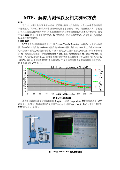
MTF、解像力测试以及相关测试方法引言:近几年,随着人们生活水平的提高,互联网交际圈的日益发达,人们对高橡素手机的需求越来越大,高像素手机镜头的市场需求量也随之水涨船高。
为此,需要评测人员对手机镜头和对应模组进行严格的评价,对模组的设计和产品的出货检验提供技术支持和保障。
我司主要从MTF测试,拍摄鉴别率测试,TV畸变测试,色彩还原性测试,杂光测试,鬼像测试以及相对照度测试等。
1.MTF测试MTF为光学调制传递函数测试,即Contrast Transfer Function,也就是:对比度转换函数。
Modulation是I的maximum减去I的minimum除以I的maximum加上I的minimum;也就是(光的最亮度减去光的最暗度)与(光的最亮度加上光的最暗度)的比值,所得出来的结果M,就是光的对比度。
物的Modulation为Mo,像的Modulation为Mi,MTF=Mi/Mo。
是利用一光强分布在空间上成正弦变化的物体经由待测系统收集并分析成像面上的光强分布(PSP),最后经由傅里叶换算所得出的结果。
它是手机模组镜头最准确的像质评测方式。
图1为测试的MTF曲线。
图1 MTF测试曲线我们公司研发实验室使用的是德国Trioptics公司的Image Master HR(研发阶段用MTF 测试仪),见图2。
车间内使用的是德国Trioptics公司的Image Master Pro5(工业性量产用MTF测试仪),见图3。
图2 Image Master HR及其操作界面图3 Image Master Pro5Image Master HR功能以及测试项目:在轴和离轴的MTF、LSF、PSF,EFL (1-50mm),ThroughFocus/Freq.(离焦),Optical Distortion,FOV(View of angle)视场角,CRA(Chief Ray Angle)主光线入射角以及Relative Illumination相对照度。
OV7725 datasheet

© 2006 OmniVision Technologies, Inc.VarioPixel, OmniVision, and the OmniVision logo are registered trademarks of OmniVision Technologies, Inc.Version 1.0, September 12, 2006OmniPixel2 and CameraChip are trademarks of OmniVision Technologies, Inc.These specifications are subject to change without notice.Advanced Information Preliminary DatasheetOV7725 Color CMOS VGA (640x480) C AMERA C HIP TM SensorO mniision®with OmniPixel2TM TechnologyGeneral DescriptionThe OV7725 C AMERA C HIP ™ image sensor is a low voltage CMOS device that provides the full functionality of a single-chip VGA camera and image processor in a small footprint package. The OV7725 provides full-frame,sub-sampled or windowed 8-bit/10-bit images in a wide range of formats, controlled through the Serial CameraApplications•Cellular and picture phones •Toys•PC Multimedia•Digital still camerasKey SpecificationsOV7725Color CMOS VGA OmniPixel2™C AMERA C HIP™ Sensor OFunctional DescriptionFigure2 shows the functional block diagram of the OV7725 image sensor. The OV7725 includes:•Image Sensor Array (total array of 656 x 488 pixels, with active pixels 640 x 480 in YUV mode)•Analog Signal Processor•A/D Converters•Test Pattern Generator•Digital Signal Processor (DSP)•Image Scaler•Timing Generator2Proprietary to OmniVision Technologies, Inc.Version 1.0, September 12, 2006Functional DescriptionVersion 1.0, September 12, 2006Proprietary to OmniVision Technologies, Inc.3OImage Sensor ArrayThe OV7725 sensor has an image array of 656x 488pixels for a total of 320,128 pixels, of which 640x 480pixels are active (307,200 pixels). Figure 3 shows a cross-section of the image sensor array.Figure 3 Image Sensor ArrayIn addition to the A/D conversion, this block also has the following functions:•Digital Black-Level Calibration (BLC)•Optional U/V channel delay •Additional A/D range controlsIn general, the combination of the A/D Range Multiplier and A/D Range Control sets the A/D range and maximum value to allow the user to adjust the final image brightness as a function of the individual application.Test Pattern GeneratorOL /I OH drive currentthe C AMERA C HIP sensor operation. Refer to OmniVision Technologies Serial Camera Control Bus (SCCB)Specification for detailed usage of the serial control port.4Proprietary to OmniVision Technologies, Inc.Version 1.0, September 12, 2006OV7725Color CMOS VGA OmniPixel2™ C AMERA C HIP ™ SensorOPin DescriptionTable 1Pin DescriptionPin NumberName Pin Type Function/DescriptionA1ADVDD Power ADC power supplyA2RSTB Input System reset input, active lowA3VREFH Reference Reference voltage - connect to ground using a 0.1 µF capacitor A4FSIN Input Frame synchronize input A5SCL Input SCCB serial interface clock input A6D0a a. D[9:0] for 10-bit Raw RGB data (D[9] MSB, D[0] LSB)Output Data output bit[0]B1ADGND Power ADC groundB2VREFN Reference Reference voltage - connect to ground using a 0.1 µF capacitor B3AVDD Power Analog power supply B4AGND Power Analog groundB5SDA I/O SCCB serial interface data I/O B6HREF Output HREF outputC1PWDN Input (0)b b. Input (0) represents an internal pull-down resistor.Power Down Mode Selection0:Normal mode1:Power down mode C6VSYNC Output Vertical sync output D1D5Output Data output bit[5]D6D4Output Data output bit[4]E1D7Output Data output bit[7]E2D1Output Data output bit[1]E3DVDD Power Power supply (+1.8 VDC) for digital logic core E4PCLK Output Pixel clock outputE5DOVDD Power Digital power supply for I/O (1.7V ~ 3.3V)E6D6Output Data output bit[6]F1D9c c. D[9:2] for 8-bit YUV or RGB565/RGB555 (D[9] MSB, D[2] LSB)Output Data output bit[9]F2D3Output Data output bit[3]F3XCLK Input System clock input F4DOGND Power Digital ground F5D2Output Data output bit[2]F6D8OutputData output bit[8]Electrical CharacteristicsVersion 1.0, September 12, 2006Proprietary to OmniVision Technologies, Inc.5OElectrical CharacteristicsNOTE:Exceeding the Absolute Maximum ratings shown above invalidates all AC and DC electrical specifications and may result in permanent device damage.Table 2Operating ConditionsParameterMin Max Operating temperature -20°C +70°C Storage temperature a a.Exceeding the stresses listed may permanently damage the device. This is a stress rating only and functional operation of the sensor at these and any other condition above those indicated in this specification is not implied. Exposure to absolute maximum rating conditions for any extended period may affect reliability.-40°C+125°CTable 3 Absolute Maximum RatingsAmbient Storage Temperature-40ºC to +95ºCSupply Voltages (with respect to Ground)V DD-A4.5 V V DD-C 3 V V DD-IO4.5 VAll Input/Output Voltages (with respect to Ground)-0.3V to V DD-IO +0.5V Lead-free Temperature, Surface-mount process 245ºCTable 4DC Characteristics (-20°C < T A < 70°C)Symbol ParameterConditionMin Typ Max Unit V DD-A DC supply voltage – Analog – 3.0 3.3 3.6V V DD-C DC supply voltage – Digital Core – 1.62 1.8 1.98V V DD-IO DC supply voltage – I/O power – 2.5– 3.3V I DDA Active (Operating) Current See Note a a. V DD-A = 3.3V, V DD-C = 1.8V, V DD-IO = 3.3VI DDA = ∑{I DD-IO + I DD-C + I DD-A }, f CLK = 24MHz at 30 fps YUV output, no I/O loading 10 + 8bb. I DD-C = 10mA, I DD-A = 8mA, without loading mA I DDS-SCCB Standby Current See Note cc. V DD-A = 3.3V, V DD-C = 1.8V, V DD-IO = 3.3VI DDS-SCCB refers to a SCCB-initiated Standby, while I DDS-PWDN refers to a PWDN pin-initiated Standby 1mA I DDS-PWDN Standby Current 1020µA V IH Input voltage HIGH CMOS0.7 x V DD-IOV V IL Input voltage LOW 0.3 x V DD-IOV V OH Output voltage HIGH CMOS0.9 x V DD-IOV V OL Output voltage LOW 0.1 x V DD-IOV I OH Output current HIGH See Note dd. Standard Output Loading = 25pF, 1.2K Ω8mA I OL Output current LOW 15mA I LInput/Output LeakageGND to V DD-IO ± 1µAOV7725Color CMOS VGA OmniPixel2™C AMERA C HIP™ Sensor OTable 5 Functional and AC Characteristics (-20°C < T A < 70°C)Symbol Parameter Min Typ Max Unit Functional CharacteristicsA/D Differential Non-Linearity+ 1/2LSBA/D Integral Non-Linearity+1LSBAGC Range30dBRed/Blue Adjustment Range12dB Inputs (PWDN, CLK, RESET#)f CLK Input Clock Frequency102448MHzt CLK Input Clock Period2142100ns t CLK:DC Clock Duty Cycle455055% t S:RESET Setting time after software/hardware reset1ms t S:REG Settling time for register change (10 frames required)300ms SCCB Timing (see Figure4)f SCL Clock Frequency400KHzt LOW Clock Low Period 1.3μs t HIGH Clock High Period600ns t AA SCL low to Data Out valid100900ns t BUF Bus free time before new START 1.3μs t HD:STA START condition Hold time600ns t SU:STA START condition Setup time600ns t HD:DAT Data-in Hold time0μs t SU:DAT Data-in Setup time100ns t SU:STO STOP condition Setup time600ns t R, t F SCCB Rise/Fall times300ns t DH Data-out Hold time50ns Outputs (VSYNC, HREF, PCLK, and D[9:0] (see Figure5, Figure6, Figure7, and Figure8)t PDV PCLK[↓] to Data-out Valid5ns t SU D[9:0] Setup time15ns t HD D[9:0] Hold time8ns t PHH PCLK[↓] to HREF[↑]05ns t PHL PCLK[↓] to HREF[↓]05nsAC Conditions:• V DD: V DD-C = 1.8V, V DD-A = 3.3V, V DD-IO = 3.3V • Rise/Fall Times: I/O: 5ns, MaximumSCCB: 300ns, Maximum • Input Capacitance: 10pf• Output Loading: 25pF, 1.2KΩ to 3.3V• f CLK: 24MHz6Proprietary to OmniVision Technologies, Inc.Version 1.0, September 12, 2006Timing SpecificationsVersion 1.0, September 12, 2006Proprietary to OmniVision Technologies, Inc.7OTiming SpecificationsFigure 4 SCCB Timing DiagramOV7725Color CMOS VGA OmniPixel2™C AMERA C HIP™ Sensor OFigure 7 QVGA Frame Timing8Proprietary to OmniVision Technologies, Inc.Version 1.0, September 12, 2006Timing SpecificationsVersion 1.0, September 12, 2006Proprietary to OmniVision Technologies, Inc.9OFigure 9 RGB 565 Output Timing DiagramOV7725Color CMOS VGA OmniPixel2™C AMERA C HIP™ Sensor OFigure 11 RGB 444 Output Timing Diagram10Proprietary to OmniVision Technologies, Inc.Version 1.0, September 12, 2006Register Set Table6 provides a list and description of the Device Control registers contained in the OV7725. For all register Enable/Disable bits, ENABLE = 1 and DISABLE = 0. The device slave addresses are 42 for write and 43 for read.Table 6 Device Control Register List (Sheet 1 of 11)Address (Hex)RegisterNameDefault(Hex)R/W Description00GAIN00RW AGC – Gain control gain settingBit[7:0]:AGC[7:0] (see GREEN[7:6] (0x03) for AGC[9:8])•Range: [00] to [FF]01BLUE80RW AWB – Blue channel gain setting •Range: [00] to [FF]02RED80RW AWB – Red channel gain setting •Range: [00] to [FF]03GREEN00RW AWB – Green channel gain setting •Range: [00] to [FF]04COM100RW Common Control 1Bit[7:2]:ReservedBit[1:0]:AGC 2 MSBs, AGC[9:8]05BAVG00RW U/B Average LevelAutomatically updated based on chip output format06GAVG00RW Y/Gb Average LevelAutomatically updated based on chip output format07RAVG00RW V/R Average LevelAutomatically updated based on chip output format08AECH00RW Exposure Value – AEC MSBsBit[7:5]:AEC[15:8] (see register AEC for AEC[7:0]} Automatically updated based on chip output format09COM201RW Common Control 2Bit[7:5]:ReservedBit[4]:Soft sleep modeBit[3:2]:Pixel clock output delay control•Range: [00] to [11]Bit[1:0]:Output drive capability00:1x01:2x10:3x11:4x0A PID77R Product ID Number MSB (Read only) 0B VER21R Product ID Number LSB (Read only)0C COM310RW Common Control 3Bit[7]:Vertical flip image ON/OFF selectionBit[6]:Horizontal mirror image ON/OFF selectionBit[5]:Swap B/R output sequence in RGB output modeBit[4]:Swap Y/UV output sequence in YUV output modeBit[3]:Swap output MSB/LSBBit[2]:Tri-state option for output clock at power-down period 0:Tri-state at this period1:No tri-state at this periodBit[1]:Tri-state option for output data at power-down period 0:Tri-state at this period1:No tri-state at this periodBit[0]:Sensor color bar test pattern output enable0D COM441RW Common Control 4Bit[7:6]:PLL frequency control00:Bypass PLL01:PLL 4x10:PLL 6x11:PLL 8xBit[5:4]:AEC evaluate window00:Full window01:1/2 window10:1/4 window11:Low 2/3 window Bit[3:0]:Reserved0E COM501RW Common Control 5Bit[7]:Auto frame rate control ON/OFF selectionBit[6]:Auto frame rate control speed selectionBit[5:4]:Auto frame rate max rate control00:No reduction of frame rate01:Max reduction to 1/2 frame rate10:Max reduction to 1/4 frame rate11:Max reduction to 1/8 frame rate Bit[3:2]:Auto frame rate active point control00:Add frame when AGC reaches 2x gain01:Add frame when AGC reaches 4x gain10:Add frame when AGC reaches 8x gain11:Add frame when AGC reaches 16x gain Bit[1]:ReservedBit[0]:AEC max step control0:AEC increase step has limit1:No limit to AEC increase step0F COM643RW Common Control 6Bit[7:1]:ReservedBit[0]:Auto window setting ON/OFF selection when format changes(Hex)Name(Hex)R/W Description10AEC40RW Exposure ValueBit[7:0]:AEC[7:0] (see register AECH for AEC[15:8])11CLKRC80RW Internal ClockBit[7]:ReservedBit[6]:Use external clock directly (no clock pre-scale available)Bit[5:0]:Internal clock pre-scalarF(internal clock) = F(input clock)/(Bit[5:0]+1)•Range: [0 0000] to [1 1111]12COM700RW Common Control 7Bit[7]:SCCB Register Reset0:No change1:Resets all registers to default values Bit[6]:Resolution selection0:VGA1:QVGABit[5]:ITU656 protocol ON/OFF selectionBit[4]:ReservedBit[3:2]:RGB output format control00:GBR4:2:201:RGB56510:RGB55511:RGB444Bit[1:0]:Output format control00:YUV01:Processed Bayer RAW10:RGB11:Bayer RAW13COM88F RW Common Control 8Bit[7]:Enable fast AGC/AEC algorithmBit[6]:AEC - Step size limit0:Step size is limited to vertical blank1:Unlimited step sizeBit[5]:Banding filter ON/OFFBit[4]:Enable AEC below banding valueBit[3]:Fine AEC ON/OFF controlBit[2]:AGC EnableBit[1]:AWB EnableBit[0]:AEC Enable(Hex)Name(Hex)R/W Description14COM94A RW Common Control 9Bit[7]:Histogram or average based AEC/AGC selection Bit[6:4]:Automatic Gain Ceiling - maximum AGC value000:2x001:4x010:8x011:16x100:32x10164x110:128x111:Not allowedBit[3]:ReservedBit[2]:Drop VSYNC output of corrupt frameBit[1]:Drop HREF output of corrupt frameBit[0]:Reserved15COM1000RW Common Control 10Bit[7]:Output negative dataBit[6]:HREF changes to HSYNCBit[5]:PCLK output option0:Free running PCLK1:PCLK does not toggle during horizontal blank Bit[4]:PCLK reverseBit[3]:HREF reverseBit[2]:VSYNC option0:VSYNC changes on falling edge of PCLK1:VSYNC changes on rising edge of PCLK Bit[1]:VSYNC negativeBit[0]:Output data range selection0:Full range1:Data from [10] to [F0] (8 MSBs)16RSVD XX–Reserved17HSTART23 (VGA)3F (QVGA)RW Horizontal Sensor Size18HSIZEA0 (VGA)50 (QVGA)RWHorizontal Frame (HREF column) end high 8-bit (low 2bits are atHREF[1:0])19VSTRT07 (VGA)03 (QVGA)RW Vertical Frame (row) start high 8-bit (low 1 bit is at HREF[6])1A VSIZEF0 (VGA)78 (QVGA)RW Vertical Sensor Size1B PSHFT40RW Data Format - Pixel Delay Select (delays timing of the D[9:0] data relative to HREF in pixel units)•Range: [00] (no delay) to [FF] (256 pixel delay which accounts for whole array)1C MIDH7F R Manufacturer ID Byte – High(Read only = 0x7F) 1D MIDL A2R Manufacturer ID Byte – Low(Read only = 0xA2) 1E RSVD XX–Reserved(Hex)Name(Hex)R/W Description1F LAEC00RW Fine AEC Value - defines exposure value less than one line period20COM1110RW Common Control 11Bit[7:2]:ReservedBit[1]:Single frame ON/OFF selection Bit[0]:Single frame transfer trigger21RSVD XX–Reserved22BDBase FF RW Banding Filter Minimum AEC Value23DBStep01RW Banding Filter Maximum Step24AEW75RW AGC/AEC - Stable Operating Region (Upper Limit) 25AEB63RW AGC/AEC - Stable Operating Region (Lower Limit)26VPT D4RW AGC/AEC Fast Mode Operating RegionBit[7:4]:High nibble of upper limit of fast mode control zone Bit[3:0]:High nibble of lower limit of fast mode control zone27RSVD XX–Reserved28REG28??RW Register 28Bit[7:2]:ReservedBit[1]:Frame sync option (in external frame sync mode, set this bit to 1)Bit[0]:Auto frame adjust option0:Always decrease frame rate by 21:Decrease frame rate by inserting dummy verticalsync equal to maximum exposure lines29HOutSize A0 (VGA)50 (QVGA)RW Horizontal Data Output Size MSBs (2 LSBs at register EXHCH[1:0])2A EXHCH00RW Dummy Pixel Insert MSBBit[7:4]: 4 MSB for dummy pixel insert in horizontal direction Bit[3]:ReservedBit[2]:Vertical data output size LSBBit[1:0]:Horizontal data output size 2 LSBs2B EXHCL00RW Dummy Pixel Insert LSB8 LSB for dummy pixel insert in horizontal direction2C VOutSize F0 (VGA)78 (QVGA)RW Vertical Data Output Size MSBs (LSB at register EXHCH[2])2D ADVFL00RW LSB of Insert Dummy Lines in Vertical Direction (1 bit equals 1 line) 2E ADVFH00RW MSB of Insert Dummy Lines in Vertical Direction2F YAVE00RW Y/G Channel Average Value30LumHTh80RW Histogram AEC/AGC Luminance High Level Threshold31LumLTh60RW Histogram AEC/AGC Luminance Low Level Threshold(Hex)Name(Hex)R/W Description32HREF00RW Image Start and Size ControlBit[7]:Mirror image edge alignmentBit[6]:Vertical HREF window start control LSBBit[5:4]:Horizontal HREF window start control LSBsBit[3]:Data output bit shift test pattern ON/OFF control Bit[2]:Vertical sensor size LSBBit[1:0]:Horizontal sensor size 2 LSBs33DM_LNL00RW Dummy Line Low 8 Bits34DM_LNH00RW Dummy Line High 8 Bits35ADoff_B80RW AD Offset Compensation Value for B Channel36ADoff_R80RW AD Offset Compensation Value for R Channel37ADoff_Gb80RW AD Offset Compensation Value for Gb Channel38ADoff_Gr80RW AD Offset Compensation Value for Gr Channel39Off_B80RW Analog Process B Channel Offset Compensation Value 3A Off_R80RW Analog Process R Channel Offset Compensation Value 3B Off_Gb80RW Analog Process Gb Channel Offset Compensation Value 3C Off_Gr80RW Analog Process Gr Channel Offset Compensation Value3D COM1280RW Common Control 12Bit[7:6]:ReservedBit[5:0]:DC offset compensation for analog process3E COM13E2RW Common Control 13Bit[7]:Analog processing channel BLC ON/OFF control Bit[6]:ADC channel BLC ON/OFF controlBit[5:0]:Reserved3F COM141F RW Edge Enhancement AdjustmentBit[7:4]:ReservedBit[3:2]:AD offset compensation optionx0:Use R/Gr channel value for B/Gb01:Use B/Gb channel value for R/Gr11:Use B/Gb/R/Gr channel value independently Bit[1:0]:Analog processing offset compensation optionx0:Use R/Gr channel value for B/Gb01:Use B/Gb channel value for R/Gr11:Use B/Gb/R/Gr channel value independently40COM15C0RW Common Control 15Bit[7:4]:ReservedBit[3]:AD add 128 bit offsetBit[2:0]:Reserved41COM1608RW Common Control 16Bit[7:2]:ReservedBit[1:0]:BLC target 2 LSBs42TGT_B80RW BLC Blue Channel Target Value (Hex)Name(Hex)R/W Description43TGT_R80RW BLC Red Channel Target Value 44TGT_Gb80RW BLC Gb Channel Target Value 45TGT_Gr80RW BLC Gr Channel Target Value46LCC000RW Lens Correction Control 0Bit[7:3]:ReservedBit[2]:Lens correction control select0:R, G, and B channel compensation coefficient isset by registers LCC3 (0x49)1:R, G, and B channel compensation coefficient isset by registers LCC5 (0x4B), LCC3 (0x49), andLCC6 (0x4C), respectivelyBit[1]:ReservedBit[0]:Lens correction enable0:Disable1:Enable47LCC100RW Lens Correction Option 1 – X Coordinate of Lens Correction Center Relative to Array Center48LCC200RW Lens Correction Option 2 – Y Coordinate of Lens Correction Center Relative to Array Center49LCC350–Lens Correction Option 3G channel compensation coefficient when LCC0[2] (0x46) is 1 R, G, and B channel compensation coefficient when LCC0[2] is 04A LCC430–Lens Correction Option 4 – radius of the circular section where no compensation applies4B LCC550RW Lens Correction Option 5 (effective only when LCC0[2] is high) 4C LCC650RW Lens Correction Option 6 (effective only when LCC0[2] is high)4D FixGain00RW Analog Fix Gain AmplifierBit[7:6]:Gb channel fixed gainBit[5:4]:Gr channel fixed gainBit[3:2]: B channel fixed gainBit[1:0]:R channel fixed gain4E AREF0EF RW Sensor Reference Control •Range: [00] to [FF]4F AREF110RW Sensor Reference Current ControlBit[7:4]:Sensor reference current controlBit[3]:Internal regulator ON/OFF selection Bit[2]:ReservedBit[1:0]:Analog reference control50AREF260RW Analog Reference Control •Range: [00] to [FF]51AREF300RW ADC Reference Control •Range: [00] to [FF]52AREF400RW ADC Reference Control •Range: [00] to [FF](Hex)Name(Hex)R/W Description53AREF524RW ADC Reference Control •Range: [00] to [FF]54AREF67A RW Analog Reference Control •Range: [00] to [FF]55AREF7FC RW Analog Reference Control •Range: [00] to [FF]56-5F RSVD XX–Reserved60UFix80RW U Channel Fixed Value Output 61VFix80RW V Channel Fixed Value Output 62AWBb_blk FF RW AWB Option for Advanced AWB63AWB_Ctrl0F0RW AWB Control Byte 0Bit[7]:AWB gain enableBit[6]:AWB calculate enableBit[5]:ReservedBit[4:0]:WBC threshold 264DSP_Ctrl11F RW DSP Control Byte 1Bit[7]:FIFO enable/disable selectionBit[6]:UV adjust function ON/OFF selectionBit[5]:YUV444 to 422 UV channel option selection Bit[4]:Color matrix ON/OFF selectionBit[3]:Interpolation ON/OFF selectionBit[2]:Gamma function ON/OFF selectionBit[1]:Black defect auto correction ON/OFFBit[0]:White defect auto correction ON/OFF65DSP_Ctrl200RW DSP Control Byte 2Bit[7:4]:ReservedBit[3:0]:Scaling control66DSP_Ctrl310RW DSP Control Byte 3Bit[7]:UV output sequence optionBit[6]:ReservedBit[5]:DSP color bar ON/OFF selectionBit[4]:ReservedBit[3]:FIFO power down ON/OFF selectionBit[2]:Scaling module power down control 1Bit[1]:Scaling module power down control 2Bit[0]:Interpolation module power down control67DSP_Ctrl400RW DSP Control Byte 468AWB_bias00RW AWB BLC Level Clip69AWBCtrl15C RW AWB Control 16A AWBCtrl211RW AWB Control 26B AWBCtrl3A2RW AWB Control 36C AWBCtrl401RW AWB Control 4(Hex)Name(Hex)R/W Description6D AWBCtrl550RW AWB Control 56E AWBCtrl680RW AWB Control 66F AWBCtrl780RW AWB Control 770AWBCtrl80F RW AWB Control 871AWBCtrl900RW AWB Control 972AWBCtrl1000RW AWB Control 1073AWBCtrl110F RW AWB Control 1174AWBCtrl120F RW AWB Control 1275AWBCtrl13FF RW AWB Control 1376AWBCtrl14FF RW AWB Control 1477AWBCtrl15FF RW AWB Control 1578AWBCtrl1610RW AWB Control 1679AWBCtrl1770RW AWB Control 177A AWBCtrl1870RW AWB Control 187B AWBCtrl19F0RW AWB Control 197C AWBCtrl20F0RW AWB Control 207D AWBCtrl21F0RW AWB Control 217E GAM10E RW Gamma Curve 1st Segment Input End Point 0x04 Output Value 7F GAM21A RW Gamma Curve 2nd Segment Input End Point 0x08 Output Value 80GAM331RW Gamma Curve 3rd Segment Input End Point 0x10 Output Value 81GAM45A RW Gamma Curve 4th Segment Input End Point 0x20 Output Value 82GAM569RW Gamma Curve 5th Segment Input End Point 0x28 Output Value 83GAM675RW Gamma Curve 6th Segment Input End Point 0x30 Output Value 84GAM77E RW Gamma Curve 7th Segment Input End Point 0x38 Output Value 85GAM888RW Gamma Curve 8th Segment Input End Point 0x40 Output Value 86GAM98F RW Gamma Curve 9th Segment Input End Point 0x48 Output Value 87GAM1096RW Gamma Curve 10th Segment Input End Point 0x50 Output Value 88GAM11A3RW Gamma Curve 11th Segment Input End Point 0x60 Output Value 89GAM12AF RW Gamma Curve 12th Segment Input End Point 0x70 Output Value 8A GAM13C4RW Gamma Curve 13th Segment Input End Point 0x90 Output Value 8B GAM14D7RW Gamma Curve 14th Segment Input End Point 0xB0 Output Value 8C GAM15E8RW Gamma Curve 15th Segment Input End Point 0xD0 Output Value8D SLOP20RW Gamma Curve Highest Segment Slope - calculated as follows: SLOP[7:0] = (0x100 - GAM15[7:0]) x 4/38E DNSTh00RW De-noise Threshold(Hex)Name(Hex)R/W Description8F EDGE000RW Edge Enhancement Control 0Bit[7:5]:ReservedBit[4:0]:Edge enhancement strength control90EDGE108RW Edge Enhancement Control 1Bit[7:4]:ReservedBit[3:0]:Edge enhancement threshold control91DNSOff10RW Auto De-noise Threshold Control92EDGE21F RW Edge Enhancement Strength Low Point Control 93EDGE301RW Edge Enhancement Strength High Point Control 94MTX12C RW Matrix Coefficient 195MTX224RW Matrix Coefficient 296MTX308RW Matrix Coefficient 397MTX414RW Matrix Coefficient 498MTX524RW Matrix Coefficient 599MTX638RW Matrix Coefficient 69A MTX_Ctrl9E RW Matrix ControlBit[7]:Matrix double ON/OFF selection Bit[6]:ReservedBit[5]:Sign bit for MTX6Bit[4]:Sign bit for MTX5Bit[3]:Sign bit for MTX4Bit[2]:Sign bit for MTX3Bit[1]:Sign bit for MTX2Bit[0]:Sign bit for MTX19B BRIGHT00RW Brightness Control9C CNST40RW Contrast Control9D CNST_ctr00RW Contrast Control Center9E UVADJ011RW Auto UV Adjust Control 0Bit[7:4]:Auto UV adjust offset control 4 LSBs Bit[3:0]:Auto UV adjust threshold control9F UVADJ102RW Auto UV Adjust Control 1Bit[7:3]:Auto UV adjust valueBit[2]:ReservedBit[1]:Auto UV adjust stop controlBit[0]:Auto UV adjust offset control MSBA0SCAL000RW Scaling Control 0A1SCAL140RW Scaling Control 1 – for horizontal scaling control A2SCAL240RW Scaling Control 2 – for vertical scaling controlA3FIFOdlyM06RW FIFO Manual Mode Delay ControlA4FIFOdlyA00RW FIFO Auto Mode Delay Control(Hex)Name(Hex)R/W DescriptionRegister SetOA5RSVD XX –ReservedA6SDE 00RW Special Digital Effect Control A7USAT 40RW U Component Saturation Control A8VSAT 40RW V Component Saturation Control A9HUE080RW Hue Control 0AAHUE180RWHue Control 1AB SIGN 06RWSign Bit for Hue and ContrastBit[7:4]:ReservedBit[3:2]:Contrast sign bit Bit[1:0]:Hue sign bitAC DSPAuto FF RWDSP Auto Function ON/OFF ControlBit[7]:AWB auto threshold control Bit[6]:De-noise auto threshold controlBit[5]:Edge enhancement auto strength control Bit[4]:UV adjust auto slope controlBit[3]:Auto scaling factor control (register SCAL0 (0xA0))Bit[2]:Auto scaling factor control (registers SCAL1 (0xA1 and SCAL2 (0xA2))Bit[1:0]:ReservedNOTE: All other registers are factory-reserved. Please contact OmniVision Technologies for reference register settings.Table 6Device Control Register List (Sheet 11 of 11)Address (Hex)Register Name Default (Hex)R/W DescriptionOV7725Color CMOS VGA OmniPixel2™ C AMERA C HIP ™ SensorOPackage SpecificationsThe OV7725 uses a 28-ball Chip Scale Package 2 (CSP2). Refer to Figure 12 for package information, Table 7 for package dimensions and Figure 13 for the array center on the chip.Figure 12 OV7725-CSP2 Package SpecificationsNote: For OVT devices that are lead-free, all part marking letters are lower case. Underlining the last digit of the lot number indicates CSP2 is used.Package SpecificationsOSensor Array CenterFigure 13 OV7725 Sensor Array CenterOV7725Color CMOS VGA OmniPixel2™C AMERA C HIP™ Sensor OChief Ray AngleFigure 14 OV7725 Chief Ray AnglePackage SpecificationsOIR Reflow Ramp Rate Requirements OV7725 Lead-Free Packaged DevicesFigure 15 IR Reflow Ramp Rate RequirementsNote: For OVT devices that are lead-free, all part marking letters are lower caseOV7725Color CMOS VGA OmniPixel2™C AMERA C HIP™ Sensor ONote:•All information shown herein is current as of the revision and publication date. Please refer to the OmniVision web site () to obtain the current versions of alldocumentation.•OmniVision Technologies, Inc. reserves the right to make changes to their products or to discontinue any product or service without further notice (It is advisable to obtain current product documentation prior to placing orders).•Reproduction of information in OmniVision product documentation and specifications is permissible only if reproduction is without alteration and is accompanied by all associatedwarranties, conditions, limitations and notices. In such cases, OmniVision is not responsibleor liable for any information reproduced.•This document is provided with no warranties whatsoever, including any warranty of merchantability, non-infringement, fitness for any particular purpose, or any warrantyotherwise arising out of any proposal, specification or sample. Furthermore, OmniVisionTechnologies, Inc. disclaims all liability, including liability for infringement of any proprietary rights, relating to use of information in this document. No license, expressed or implied, byestoppels or otherwise, to any intellectual property rights is granted herein.•‘OmniVision’, ’VarioPixel’ and the OmniVision logo are registered trademarks of OmniVision Technologies, Inc. ’OmniPixel2’ and ’CameraChip’ are trademarks of OmniVision Technologies, Inc. All other trade, product or service names referenced in this release may be trademarks or registered trademarks of their respective holders. Third-party brands, names, and trademarks are the property of their respective owners.For further information, please feel free to contact OmniVision at info@.OmniVision Technologies, Inc.1341 Orleans DriveSunnyvale, CA USA(408) 542-3000。
PFUlimited 2022年版FI-8150扫描仪说明书

E ciency optimized, simplicity achie v ed, with expanded software functionalities The scanner driver, PaperStream IP, comes with a simplified, user-friendly interface thatprovides icon visibility for easy setting config-urations. Users can consistently achieve scanned outputs of correct orientations withthe "Automatic Rotation" function, and store frequently scanned documents in specific formats using the "pattern matching" method.Efficiency with simplification brings users, a reduction to operation time as well on frequent and routine operations like deleting blank pages, or correcting page orientations, just by following the optimal settings suggest-ed by the “Settings Assistant” on the integrat-ed PaperStream Capture software. Documents can be retrieved more efficiently with the "PDFkeyword setting" function, instead of being constrained to file names alone.Optimized high-quality imagesThe fi-8150 comes with “Clear Image Capture”, a unique and dedicated image correction technology that generates unparalleled, high-definition images while keeping power consumption to the minimum. Quality images with no missing edges can be ensured with the scanner’s Skew Reducer mechanism.Better usability and exibility for any environ-mentThe fi-8150 supports multiple operation modes according to users’ environments, may that require sharing among teams with PC-less colleagues, or LAN connectivity and USB 3.2.The flexibility to use with imprinter options opens up the capability for total document management and assists in documentarchiving requirements that are prevalent in many industries. Reliable. State-of-art feeding and optical technologies.Quality images. The best you can get.Paper handling. Scan with confidence.State-of-art feeding technology - streamline work owIn the “Manual Feed Mode”, the fi-8150 scanscopy forms and passports or booklets up to thicknesses of 7 mm with the carrier sheet. Precise multi-feed detection on a wide range of documents like plastic cards and documents with attachments, enable contin-ual scanning with the same profiles. In addition, the “Automatic Separation Control” optimizes paper feed to match the number of sheets loaded, preventing interruptions. “Image Monitoring” also performs checks, real-time, for image skews, and providesenhanced paper protection.Efficiency at new heights with evolved feedingDatasheetFUJITSU Image Scanner fi-8150Datasheet FUJITSU Image Scanner fi-8150ContactTrademarksISIS is a trademark of Open Text. Microsoft, Windows, and Windows Server are either registered trademarks or trademarks of Microsoft Corporation in the United States and/or other countries. macOS is a trademark of Apple Inc., registered in the U.S. and other countries. Linux is the registered trademark of Linus Torvalds in the U.S. and other countries. Any other products or company names appearing in this document are the trademarks or registered trademarks of the respective companies.Safety PrecautionsPlease carefully read the safety precautions prior to the use of this device and follow the recommended instructions for correct use. Do not place this device in wet, moist, highly humid, dusty or oily areas. Use of this device under such conditions may result in electrical shock, fire or damage to the device. Please use this device within the power ratings listed.ENERGY STAR®PFU Limited, a Fujitsu company, has determined that this product meets the ENERGY STAR® guidelines for energy efficiency. ENERGY STAR® is a registered trademark of the United States.Specifications are subject to change without notice. Visit your local Fujitsu website for more information.*1 Actual scanning speeds may vary with data transmission and software processing times. *2 Indicated speeds are from using JPEG compression. *3 Indicated speeds are from using TIFF CCITT Group 4 compression.*4 Selectable maximum resolution may vary depending on the length of the scanned document. *5 Limitations may apply to the size of documents that can be scanned, depending on system environment, when scanning at high resolution (over 600 dpi). *6 Maximum document width possible for scanning is 240 mm (9.5 inch). *7 For use with PaperStream NX Manager, the maximum resolution supported is 400 dpi, with maximum lengths ranging with resolution. Simplex: 1,828.8 mm (72 in.) [below 300 dpi], 355.6 mm (14 in.) [below 400 dpi]. Duplex: 863.6 mm (34 in.) [below 300 dpi], 355.6 mm (14 in.) [below 400 dpi]. *8 Thicknesses of up to 128 to 209 g/m² (34 to 56 lb) can be scanned for A8 (52 x 74 mm / 2.1 x 2.9 inch) sizes. *9 Booklet scanning requires use of Booklet Carrier Sheets. Indicated thickness is inclusive of Booklet Carrier Sheet thickness. *10 Continuous feeding is supported when scanning up to 10 unembossed cards with thicknesses of 0.76 mm or less. *11 Maximum capacity depends on paper weight and may vary. *12 Capable of setting additional documents while scanning. *13 Numbers are calculated using scanning speeds and typical hours of scanner use, and are not meant to guarantee daily volume or unit durability. *14 Excludes the ADF paper chute and stacker. *15 Functions equivalent to those offered by PaperStream IP may not be available with the Image Scanner Driver for macOS/Linux or WIA Driver. *16 Refer to the fi Series Support Site for driver/software downloads and full lineup of all supported operating system versions. https:///global/support/products/computing/peripheral/scanners/fi/.4,000,000 printed characters or 6 months after opening the packageCA00050-0262Print CartridgeEvery 200,000 sheets or one year PA03670-0002Pick Roller Every 200,000 sheets or one year PA03810-0001Brake Roller ConsumablesPaperStream Capture Pro optional licensePA43404-A665PaperStream Capture Pro Scan Station (WG)Reads PDF417, QR code, Data Matrix, Aztec CodePA43404-A4332D Barcode for PaperStreamPack of single sheetPA03810-0020Booklet Carrier Sheet Pack of 3 sheets PA03770-0015 Photo Carrier Sheets Pack of 5 sheets PA03360-0013 Carrier Sheets Prints on the back of the document PA03810-D201 Post Imprinter (FI-819PRB) OptionsADF paper chute, AC cable, AC adapter, USB cable, Setup DVD-ROMIncluded ItemsMulti image output, Automatic color detection, Blank page detection, Dynamic threshold (iDTC), Advanced DTC, SDTC,Error diffusion, Dither, De-Screen, Emphasis, Dropout color (None/Red/Green/Blue/White/Saturation/Custom), sRGBoutput, Hole punch removal, Index tab cropping, Split image,De-Skew, Edge filler, Vertical streaks reduction, Background pattern removal, Cropping, Static thresholdImage Processing FunctionsPaperStream IP Driver (TWAIN/TWAIN x64/ISIS), WIA Driver *¹⁵, Image Scanner Driver for macOS (ICA)*¹⁵*¹⁶, Image Scanner Driver for Linux (SANE)*¹⁵*¹⁶, PaperStream Capture,PaperStream ClickScan *¹⁶, Software Operation Panel, Error Recovery Guide, ABBYY FineReader for ScanSnap™*16, Scanner Central AdminIncluded Software / DriversWindows® 11, Windows® 10, Windows® 8.1, Windows® 7, Windows Server® 2022, Windows Server® 2019, Windows Server® 2016, Windows Server® 2012 R2, Windows Server® 2012, Windows Server® 2008 R2, macOS, Linux (Ubuntu)Supported Operating System4 kg (8.8 lb)Weight300 x 170 x 163 mm (11.8 x 6.7 x 6.4 inch )Dimensions *¹⁴(Width x Depth x Height)ENERGY STAR®, RoHSEnvironmental Compliance 15 to 80% (non-condensing)Relative Humidity5 to 35 °C (41 to 95 °F)Temperature Operating Environment 0.2 W or lessAuto Standby (Off) Mode 2.0 W or less (LAN) / 1.4 W or less (USB)Sleep Mode21 W or less / 17 W (Eco mode)Operating Mode Power Consumption AC 100V - 240V 50/60 Hz Power Requirements 10BASE-T, 100BASE-TX, 1000BASE-T EthernetUSB 3.2 Gen1x1 / USB 2.0 / USB 1.1USB Interface Image monitoringPaper Protection Overlap detection (Ultrasonic sensor), Length detection Multifeed Detection 8,000 sheetsExpected Daily Volume *¹³100 sheets (A4 80 g/m² or Letter 20 lb)ADF Capacity *¹¹*¹²Less than 7 mm (0.276 inch )*⁹20 to 465 g/m² (5.3 to 124 lb)*⁸Plastic Card 1.4 mm (0.055 inch ) or less *¹⁰Booklet Paper Paper Weight (Thickness)6,096 mm (240 inch )Long Page Scanning *⁷48 x 50 mm (1.9 x 2 inch)Minimum215.9 x 355.6 mm (8.5 x 14 inch)Maximum *⁶Document Size White / Black (selectable)Background Colors Color: 24-bit, Grayscale: 8-bit, Monochrome: 1-bit Output Format 50 to 600 dpi (adjustable by 1 dpi increments),1,200 dpi (driver)*⁵Output Resolution *⁴(Color / Grayscale / Monochrome)600 dpiOptical ResolutionRGB LED x 2 (front x 1, back x 1)Light Source CIS x 2 (front x 1, back x 1)Image Sensor Type Simplex: 50 ppm (200/300 dpi)Duplex: 100 ipm (200/300 dpi)Scanning Speed *¹ (A4 Portrait)(Color *²/Grayscale *²/Monochrome *³)ADF (Automatic Document Feeder) / Manual Feed, DuplexScanner TypeTechnical InformationDatasheet FUJITSU Image Scanner fi-8150IndonesiaPT Fujitsu Indonesia Tel: +62 21 570 9330*************************/id/scannersMalaysiaFujitsu (Malaysia) Sdn Bhd Tel: +603 8230 4188askfujitsu .my @/my/scannersPhilippinesFujitsu Philippines, Inc. Tel: +63 2 841 8488 ***************.com/ph/scannersSingaporeFujitsu Asia Pte Ltd Tel: +65 6512 7555 *******************/sg/scannersThailandFujitsu (Thailand) Co., Ltd. Tel: +66 2 302 1500 info .th @/th/en/scannersVietnamFujitsu Vietnam Limited Tel: + 84 4 2220 3113 sales -vn @/vn/en/scanners。
NanoString质量控制仪表板版本2.0.5说明书

Package‘NACHO’August7,2023Type PackageTitle NanoString Quality Control DashboardVersion2.0.5Description NanoString nCounter data are gene expression assayswhere there is no need for the use of enzymes or amplificationprotocols and work withfluorescent barcodes(Geiss et al.(2018)<doi:10.1038/nbt1385>).Each barcode is assigned amessenger-RNA/micro-RNA(mRNA/miRNA)which after bonding with itstarget can be counted.As a result each count of a specific barcoderepresents the presence of its target mRNA/miRNA.'NACHO'(NAnoStringquality Control dasHbOard)is able to analyse the exported NanoStringnCounter data and facilitates the user in performing a qualitycontrol.'NACHO'does this by visualising quality control metrics,expression of control genes,principal components and sample specificsize factors in an interactive web application.License GPL-3URL https:///mcanouil/NACHO/,https://m.canouil.dev/NACHO/ BugReports https:///mcanouil/NACHO/issuesDepends R(>=3.6.0)Imports utils,data.table,ggplot2(>=3.3.0),ggforce(>=0.3.1),ggrepel(>=0.8.1),knitr(>=1.25),rmarkdown(>=1.16),shiny(>=1.4.0),shinyWidgets(>=0.4.9)Suggests roxygen2(>=7.2.0),testthat(>=2.2.1),covr(>=3.3.2),Biobase,GEOquery,limmaVignetteBuilder knitrEncoding UTF-8LazyData trueRoxygenNote7.2.3SystemRequirements pandoc(>=1.12.3),pandoc-citeprocConfig/testthat/edition31NeedsCompilation noAuthor Mickaël Canouil[aut,cre](<https:///0000-0002-3396-4549>), Roderick Slieker[aut](<https:///0000-0003-0961-9152>),Gerard Bouland[aut]Maintainer Mickaël Canouil<*******************.dev>Repository CRANDate/Publication2023-08-0719:30:09UTCR topics documented:autoplot.nacho (2)check_outliers (4)deploy (4)GSE74821 (5)load_rcc (5)normalise (7)print.nacho (10)render (12)visualise (13)Index15 autoplot.nacho Plot quality-control metrics and thresholds of a"nacho"objectDescriptionThis function allows to plot any qualit-controlfigures available within the shiny app using visualise() or in the HTML report from render().Usage##S3method for class nachoautoplot(object,x,colour="CartridgeID",size=0.5,show_legend=TRUE,show_outliers=TRUE,outliers_factor=1,outliers_labels=NULL,...)Argumentsobject[list]List obtained from load_rcc()or normalise().x[character]Character string naming the quality-control metrics to plot from nacho_object.The possible values are:•"BD"(Binding Density)•"FoV"(Imaging)•"PCL"(Positive Control Linearity)•"LoD"(Limit of Detection)•"Positive"(Positive Controls)•"Negative"(Negative Controls)•"Housekeeping"(Housekeeping Genes)•"PN"(Positive Controls vs.Negative Controls)•"ACBD"(Average Counts vs.Binding Density)•"ACMC"(Average Counts vs.Median Counts)•"PCA12"(Principal Component1vs.2)•"PCAi"(Principal Component scree plot)•"PCA"(Principal Components planes)•"PFNF"(Positive Factor vs.Negative Factor)•"HF"(Housekeeping Factor)•"NORM"(Normalisation Factor)colour[character]Character string of the column in ssheet_csv or more generally in nacho_object$nacho to be used as grouping colour.size[numeric]A numeric controlling point size(ggplot2::geom_point()or line size(ggplot2::geom_line()).show_legend[logical]Boolean to indicate whether the plot legends should be plotted(TRUE) or not(FALSE).Default is TRUE.show_outliers[logical]Boolean to indicate whether the outliers should be highlighted in red (TRUE)or not(FALSE).Default is TRUE.outliers_factor[numeric]Size factor for outliers compared to size.Default is1.outliers_labels[character]Character to indicate which column in nacho_object$nacho shouldbe used to be printed as the labels for outliers or not.Default is NULL....Other arguments(Not used).Examplesdata(GSE74821)autoplot(GSE74821,x="BD")4deploy check_outliers Annotate a"nacho"object for outliersDescriptionAdd or update"is_outlier"column in the"nacho"field of an object from a call to load_rcc() or normalise()(nacho_object$nacho),using the current quality-control thresholds.Usagecheck_outliers(nacho_object)Argumentsnacho_object[list]A list object of class"nacho"obtained from load_rcc()or normalise(). ValueA[list]object of class"nacho".Examplesdata(GSE74821)nacho_object<-check_outliers(GSE74821)head(nacho_object$nacho)deploy Deploy(copy)the shiny application to the specified directoryDescriptionDeploy(copy)the shiny application to the specified directoryUsagedeploy(directory="/srv/shiny-server",app_name="NACHO")Argumentsdirectory[character]A character vector of one path to the new location.app_name[character]A character vector defining the shiny application name in the new location.GSE748215 Value[logical]A logical indicating whether the deployment is successfull(TRUE)or not(FALSE). Examplesdeploy(directory=".")if(interactive()){shiny::runApp("NACHO")}GSE74821A"nacho"object containing20samples of GSE74821datasetDescriptionNanoString nCounter RUO-PAM50Gene Expression Custom CodeSetUsageGSE74821FormatA[list]object of class"nacho".SourceGSE74821load_rcc Produce a"nacho"object from RCC NanoStringfilesDescriptionThis function is used to preprocess the data from NanoString nCounter.6load_rccUsageload_rcc(data_directory,ssheet_csv,id_colname=NULL,housekeeping_genes=NULL,housekeeping_predict=FALSE,housekeeping_norm=TRUE,normalisation_method="GEO",n_comp=10)Argumentsdata_directory[character]A character string of the directory where the data are stored.ssheet_csv[character]or[data.frame]Either a string with the name of the CSV of the sam-plesheet or the samplesheet as a data.frame.Should contain a column thatmatches thefile names in the folder.id_colname[character]Character string of the column in ssheet_csv that matches thefile names in data_directory.housekeeping_genes[character]A vector of names of the miRNAs/mRNAs that should be used ashousekeeping genes.Default is NULL.housekeeping_predict[logical]Boolean to indicate whether the housekeeping genes should be pre-dicted(TRUE)or not(FALSE).Default is FALSE.housekeeping_norm[logical]Boolean to indicate whether the housekeeping normalisation should beperformed.Default is TRUE.normalisation_method[character]Either"GEO"or"GLM".Character string to indicate normalisation us-ing the geometric mean("GEO")or a generalized linear model("GLM").Defaultis"GEO".n_comp[numeric]Number indicating the number of principal components to compute.Cannot be more than n-1samples.Default is10.Value[list]A list object of class"nacho":access[character]Value passed to load_rcc()in id_colname.housekeeping_genes[character]Value passed to load_rcc().housekeeping_predict[logical]Value passed to load_rcc().housekeeping_norm[logical]Value passed to load_rcc().normalisation_method[character]Value passed to load_rcc().remove_outliers[logical]FALSE.n_comp[numeric]Value passed to load_rcc().data_directory[character]Value passed to load_rcc().pc_sum[data.frame]A data.frame with n_comp rows and four columns:"Standard deviation", "Proportion of Variance","Cumulative Proportion"and"PC".nacho[data.frame]A data.frame with all columns from the sample sheet ssheet_csv and all computed columns,i.e.,quality-control metrics and counts,with one sample per row.outliers_thresholds[list]A list of the(default)quality-control thresholds used. Examplesif(interactive()){library(GEOquery)library(NACHO)#Import data from GEOgse<-GEOquery::getGEO(GEO="GSE74821")targets<-Biobase::pData(Biobase::phenoData(gse[[1]]))GEOquery::getGEOSuppFiles(GEO="GSE74821",baseDir=tempdir())utils::untar(tarfile=file.path(tempdir(),"GSE74821","GSE74821_RAW.tar"),exdir=file.path(tempdir(),"GSE74821"))targets$IDFILE<-list.files(path=file.path(tempdir(),"GSE74821"),pattern=".RCC.gz$")targets[]<-lapply(X=targets,FUN=iconv,from="latin1",to="ASCII")utils::write.csv(x=targets,file=file.path(tempdir(),"GSE74821","Samplesheet.csv"))#Read RCC files and formatnacho<-load_rcc(data_directory=file.path(tempdir(),"GSE74821"),ssheet_csv=file.path(tempdir(),"GSE74821","Samplesheet.csv"),id_colname="IDFILE")}normalise(re)Normalise a"nacho"objectDescriptionThis function creates a list in which your settings,the raw counts and normalised counts are stored, using the result from a call to load_rcc().Usagenormalise(nacho_object,housekeeping_genes=nacho_object[["housekeeping_genes"]],housekeeping_predict=nacho_object[["housekeeping_predict"]],housekeeping_norm=nacho_object[["housekeeping_norm"]],normalisation_method=nacho_object[["normalisation_method"]],n_comp=nacho_object[["n_comp"]],remove_outliers=nacho_object[["remove_outliers"]],outliers_thresholds=nacho_object[["outliers_thresholds"]])Argumentsnacho_object[list]A list object of class"nacho"obtained from load_rcc()or normalise().housekeeping_genes[character]A vector of names of the miRNAs/mRNAs that should be used ashousekeeping genes.Default is NULL.housekeeping_predict[logical]Boolean to indicate whether the housekeeping genes should be pre-dicted(TRUE)or not(FALSE).Default is FALSE.housekeeping_norm[logical]Boolean to indicate whether the housekeeping normalisation should beperformed.Default is TRUE.normalisation_method[character]Either"GEO"or"GLM".Character string to indicate normalisation us-ing the geometric mean("GEO")or a generalized linear model("GLM").Defaultis"GEO".n_comp[numeric]Number indicating the number of principal components to compute.Cannot be more than n-1samples.Default is10.remove_outliers[logical]A boolean to indicate if outliers should be excluded.outliers_thresholds[list]List of thresholds to exclude outliers.DetailsOutliers definition(remove_outliers=TRUE):•Binding Density(BD)<0.1•Binding Density(BD)>2.25•Field of View(FoV)<75•Positive Control Linearity(PCL)<0.95•Limit of Detection(LoD)<2•Positive normalisation factor(Positive_factor)<0.25•Positive normalisation factor(Positive_factor)>4•Housekeeping normalisation factor(house_factor)<1/11•Housekeeping normalisation factor(house_factor)>11Value[list]A list containing parameters and data.access[character]Value passed to load_rcc()in id_colname.housekeeping_genes[character]Value passed to load_rcc()or normalise().housekeeping_predict[logical]Value passed to load_rcc().housekeeping_norm[logical]Value passed to load_rcc()or normalise().normalisation_method[character]Value passed to load_rcc()or normalise().remove_outliers[logical]Value passed to normalise().n_comp[numeric]Value passed to load_rcc().data_directory[character]Value passed to load_rcc().pc_sum[data.frame]A data.frame with n_comp rows and four columns:"Standard deviation", "Proportion of Variance","Cumulative Proportion"and"PC".nacho[data.frame]A data.frame with all columns from the sample sheet ssheet_csv and all computed columns,i.e.,quality-control metrics and counts,with one sample per row.outliers_thresholds[list]A list of the quality-control thresholds used.raw_counts[data.frame]Raw counts with probes as rows and samples as columns.With"CodeClass"(first column),the type of the probes and"Name"(second column),the Name of the probes.normalised_counts[data.frame]Normalised counts with probes as rows and samples as columns.With"CodeClass"(first column)),the type of the probes and"Name"(second column),thename of the probes.Examplesdata(GSE74821)GSE74821_norm<-normalise(nacho_object=GSE74821,housekeeping_norm=TRUE,normalisation_method="GEO",remove_outliers=TRUE)if(interactive()){library(GEOquery)library(NACHO)#Import data from GEOgse<-GEOquery::getGEO(GEO="GSE74821")targets<-Biobase::pData(Biobase::phenoData(gse[[1]]))GEOquery::getGEOSuppFiles(GEO="GSE74821",baseDir=tempdir())10print.nacho utils::untar(tarfile=file.path(tempdir(),"GSE74821","GSE74821_RAW.tar"),exdir=file.path(tempdir(),"GSE74821"))targets$IDFILE<-list.files(path=file.path(tempdir(),"GSE74821"),pattern=".RCC.gz$")targets[]<-lapply(X=targets,FUN=iconv,from="latin1",to="ASCII")utils::write.csv(x=targets,file=file.path(tempdir(),"GSE74821","Samplesheet.csv"))#Read RCC files and formatnacho<-load_rcc(data_directory=file.path(tempdir(),"GSE74821"),ssheet_csv=file.path(tempdir(),"GSE74821","Samplesheet.csv"),id_colname="IDFILE")#(re)Normalise data by removing outliersnacho_norm<-normalise(nacho_object=nacho,remove_outliers=TRUE)#(re)Normalise data with"GLM"method and removing outliersnacho_norm<-normalise(nacho_object=nacho,normalisation_method="GLM",remove_outliers=TRUE)}print.nacho Print method for"nacho"objectDescriptionThis function allows to print text andfigures from the results of a call to load_rcc()or normalise().It is intended to be used in a Rmarkdown chunk.Usage##S3method for class nachoprint(x,colour="CartridgeID",print.nacho11 size=0.5,show_legend=FALSE,show_outliers=TRUE,outliers_factor=1,outliers_labels=NULL,echo=FALSE,title_level=1,xaringan=FALSE,...)Argumentsx[list]A list object of class"nacho"obtained from load_rcc()or normalise().colour[character]Character string of the column in ssheet_csv or more generally in nacho_object$nacho to be used as grouping colour.size[numeric]A numeric controlling point size(ggplot2::geom_point()or line size(ggplot2::geom_line()).show_legend[logical]Boolean to indicate whether the plot legends should be plotted(TRUE) or not(FALSE).Default is TRUE.show_outliers[logical]Boolean to indicate whether the outliers should be highlighted in red (TRUE)or not(FALSE).Default is TRUE.outliers_factor[numeric]Size factor for outliers compared to size.Default is1.outliers_labels[character]Character to indicate which column in nacho_object$nacho shouldbe used to be printed as the labels for outliers or not.Default is NULL.echo[logical]A boolean to indicate whether text and plots should be printed.Mainly for use within a Rmarkdown chunk.title_level[numeric]A numeric to indicate the title level to start with,using markdown style,i.e.,the number of"#".xaringan[logical]A boolean to format output for Xaringan slides....Other arguments(Not used).Examplesdata(GSE74821)print(GSE74821)12render render Render a HTML report of a"nacho"objectDescriptionThis function create a Rmarkdown script and render it as a HTML document.The HTML document is a quality-control report using all the metrics from visualise()based on recommendations from NanoString.Usagerender(nacho_object,colour="CartridgeID",output_file="NACHO_QC.html",output_dir=".",size=1,show_legend=TRUE,show_outliers=TRUE,outliers_factor=1,outliers_labels=NULL,clean=TRUE)Argumentsnacho_object[list]A list object of class"nacho"obtained from load_rcc()or normalise().colour[character]Character string of the column in ssheet_csv or more generally in nacho_object$nacho to be used as grouping colour.output_file[character]The name of the outputfile.output_dir[character]The output directory for the rendered output_file.This allows for a choice of an alternate directory to which the outputfile should be written(thedefault output directory is the working directory,i.e.,.).If a path is providedwith afilename in output_file the directory specified here will take prece-dence.Please note that any directory path provided will create any necessarydirectories if they do not exist.size[numeric]A numeric controlling point size(ggplot2::geom_point()or line size(ggplot2::geom_line()).show_legend[logical]Boolean to indicate whether the plot legends should be plotted(TRUE) or not(FALSE).Default is TRUE.show_outliers[logical]Boolean to indicate whether the outliers should be highlighted in red (TRUE)or not(FALSE).Default is TRUE.outliers_factor[numeric]Size factor for outliers compared to size.Default is1.outliers_labels[character]Character to indicate which column in nacho_object$nacho shouldbe used to be printed as the labels for outliers or not.Default is NULL.clean[logical]Boolean to indicate whether the Rmd and Rdatafile used to produce the HTML report are removed from output_dir.Default is TRUE.Examplesif(interactive()){data(GSE74821)render(GSE74821)}visualise Visualise quality-control metrics of a"nacho"objectDescriptionThis function allows to visualise results from load_rcc()or normalise()several quality-control metrics in an interactive shiny application,in which thresholds can be customised and exported.Usagevisualise(nacho_object)Argumentsnacho_object[list]A list object of class"nacho"obtained from load_rcc()or normalise(). Examplesif(interactive()){data(GSE74821)#Must be run in an interactive R session!visualise(GSE74821)}if(interactive()){library(GEOquery)library(NACHO)#Import data from GEOgse<-GEOquery::getGEO(GEO="GSE74821")targets<-Biobase::pData(Biobase::phenoData(gse[[1]]))GEOquery::getGEOSuppFiles(GEO="GSE74821",baseDir=tempdir())utils::untar(tarfile=file.path(tempdir(),"GSE74821","GSE74821_RAW.tar"),exdir=file.path(tempdir(),"GSE74821"))targets$IDFILE<-list.files(path=file.path(tempdir(),"GSE74821"),pattern=".RCC.gz$")targets[]<-lapply(X=targets,FUN=iconv,from="latin1",to="ASCII") utils::write.csv(x=targets,file=file.path(tempdir(),"GSE74821","Samplesheet.csv"))#Read RCC files and formatnacho<-load_rcc(data_directory=file.path(tempdir(),"GSE74821"),ssheet_csv=file.path(tempdir(),"GSE74821","Samplesheet.csv"),id_colname="IDFILE")visualise(nacho)#(re)Normalise data by removing outliersnacho_norm<-normalise(nacho_object=nacho,remove_outliers=TRUE)visualise(nacho_norm)#(re)Normalise data with"GLM"method and removing outliersnacho_norm<-normalise(nacho_object=nacho,normalisation_method="GLM",remove_outliers=TRUE)visualise(nacho_norm)}Index∗datasetsGSE74821,5autoplot.nacho,2character,3,4,6–9,11–13check_outliers,4data.frame,6,7,9deploy,4ggplot2::geom_line(),3,11,12ggplot2::geom_point(),3,11,12GSE74821,5list,3–9,11–13load_rcc,5load_rcc(),3,4,6–13logical,3,5,6,8,9,11–13normalise,7normalise(),3,4,8–13normalize(normalise),7numeric,3,6–9,11,12print.nacho,10render,12render(),2visualise,13visualise(),2,12visualize(visualise),1315。
AXIS M3088-V 8 MP мини胶囊摄像机说明书
AXIS M3088-V Dome CameraFixed8MP mini dome with deep learningThis cost-efficient mini dome features Wide Dynamic Range(WDR)to ensure clarity even when there’s both dark and light areas in the scene.A deep learning processing unit enables intelligent analytics based on deep learning on the edge.Plus,AXIS Object Analytics including time in area feature lets you track whenever an object stays in a defined area longer than a user-defined time,for example,to detect loitering.This compact,easy-to-install,vandal-resistant camera comes factory focused so there’s no manual focusing required.Furthermore,Axis Edge Vault protects your Axis device ID and simplifies authorization of Axis devices on your network.>Great image quality in8MP>Compact,discreet design>WDR for challenging light>Support for analytics with deep learning>Built-in cybersecurity featuresDatasheetAXIS M3088-V Dome Camera CameraImage sensor1/2.8”progressive scan RGB CMOSLens 2.9mm,F2.0Horizontal field of view:109°Vertical field of view:56°Fixed iris,IR correctedDay and night Automatically removable infrared-cut filterMinimum illumination Color:0.25lux at50IRE F2.0 B/W:0.05lux at50IRE F2.0Shutter speed1/71500s to1/5sCamera angle adjustment Pan:±175°Tilt:±80°Rotation:±175°Can be directed in any direction and see the wall/ceilingSystem on chip(SoC)Model CV25Memory2048MB RAM,512MB Flash ComputecapabilitiesDeep learning processing unit(DLPU) VideoVideo compression H.264(MPEG-4Part10/AVC)Main and High Profiles H.265(MPEG-H Part2/HEVC)Main Profile Motion JPEGResolution3840x2160(8MP)to320x240Frame rate12/15fps with power line frequency50/60Hz in H.264andH.265aVideo streaming Multiple,individually configurable streams in H.264,H.265and Motion JPEGAxis Zipstream technology in H.264and H.265Controllable frame rate and bandwidthVBR/MBR H.264/H.265Average bitrateMulti-viewstreamingUp to2individually cropped out view areas in full frame rateImage settings Compression,color,brightness,sharpness,contrast,whitebalance,exposure control,motion-adaptive exposure,WDR:upto120dB depending on scene,dynamic overlays,mirroring ofimages,privacy maskRotation:0°,90°,180°,270°,including Corridor FormatPan/Tilt/Zoom Digital PTZAudioAudio input/output Audio features through portcast technology:two-way audio connectivity,voice enhancerNetworkNetwork protocols IPv4,IPv6USGv6,ICMPv4/ICMPv6,HTTP,HTTPS,HTTP/2,TLS,QoS Layer3DiffServ,FTP,SFTP,CIFS/SMB,SMTP,mDNS(Bonjour), UPnP®,SNMP v1/v2c/v3(MIB-II),DNS/DNSv6,DDNS,NTP, NTS,RTSP,RTCP,RTP,SRTP/RTSPS,TCP,UDP,IGMPv1/v2/v3, DHCPv4/v6,SSH,LLDP,CDP,MQTT v3.1.1,Secure syslog(RFC 3164/5424,UDP/TCP/TLS),Link-Local address(ZeroConf)System integrationApplication Programming Interface Open API for software integration,including VAPIX®and AXIS Camera Application Platform;specifications at One-click cloud connectionONVIF®Profile G,ONVIF®Profile M,ONVIF®Profile S,and ONVIF®Profile T,specification at Event conditions Device status:above operating temperature,above or belowoperating temperature,below operating temperature,IP addressremoved,live stream active,network lost,new IP address,systemready,within operating temperatureEdge storage:recording ongoing,storage disruption,storagehealth issues detectedI/O:manual trigger,virtual input,digital input via accessoriesusing portcast technologyMQTT:subscribeScheduled and recurring:scheduleVideo:average bitrate degradation,tampering Event actions Notification:HTTP,HTTPS,TCP and emailRecord video:SD card and network shareMQTT:publishPre-and post-alarm video or image buffering for recording oruploadRecord video:SD card and network shareSNMP traps:send,send while the rule is activeUpload of images or video clips:FTP,SFTP,HTTP,HTTPS,networkshare and emailExternal output activation via accessories using portcasttechnologyBuilt-ininstallation aidsPixel counterAnalyticsAXIS ObjectAnalyticsObject classes:humans,vehicles(types:cars,buses,trucks,bikes)Features:line crossing,object in area,crossline counting BETA,occupancy in area BETA,time in area BETAUp to10scenariosMetadata visualized with color-coded bounding boxesPolygon include/exclude areasPerspective configurationONVIF Motion Alarm eventMetadata Object data:Classes:humans,faces,vehicles(types:cars,buses, trucks,bikes),license platesAttributes:Vehicle color,upper/lower clothing color,confidence,positionEvent data:Producer reference,scenarios,trigger conditions Applications IncludedAXIS Object Analytics,AXIS Video Motion DetectionSupport for AXIS Camera Application Platform enablinginstallation of third-party applications,see /acap CybersecurityEdge security Software:Signed firmware,brute force delay protection,digest authentication,password protection,AES-XTS-Plain64256bitSD card encryptionHardware:Axis Edge Vault cybersecurity platformSecure element(CC EAL6+),system-on-chip security(TEE),Axisdevice ID,secure keystore,signed video,secure boot,encryptedfilesystem(AES-XTS-Plain64256bit)Network security IEEE802.1X(EAP-TLS),IEEE802.1AR,HTTPS/HSTS,TLS v1.2/v1.3, Network Time Security(NTS),X.509Certificate PKI,IP addressfilteringDocumentation AXIS OS Hardening GuideAxis Vulnerability Management PolicyAxis Security Development ModelAXIS OS Software Bill of Material(SBOM)To download documents,go to /support/cybersecu-rity/resourcesTo read more about Axis cybersecurity support,go to/cybersecurityGeneralCasing IP42water-and dust-resistant(to comply with IP42,followInstallation Guide),IK08impact-resistant,polycarbonate/ABScasingEncapsulated electronicsColor:white NCS S1002-BFor repainting instructions,contact your Axis partner. Sustainability57%recycled plastics,PVC free,BFR/CFR freePower Power over Ethernet(PoE)IEEE802.3af/802.3at Type1Class2Typical3.6W,max4.2WConnectors RJ4510BASE-T/100BASE-TX PoEAudio:Audio and I/O connectivity via portcast technology Storage Support for microSD/microSDHC/microSDXC cardSupport for SD card encryption(AES-XTS-Plain64256bit)Recording to network-attached storage(NAS)For SD card and NAS recommendations see Operatingconditions0°C to40°C(32°F to104°F)Humidity10–85%RH(non-condensing)Storageconditions-40°C to65°C(-40°F to149°F)Humidity5–95%RH(non-condensing)Approvals EMCICES-3(A)/NMB-3(A),EN55032Class A,EN55035,EN61000-6-1,EN61000-6-2,FCC Part15Subpart B Class A,ICES-003Class A,VCCI Class A,KS C9835,KS C9832Class A,RCM AS/NZS CISPR32Class A,SafetyIEC/EN/UL62368-1,IS13252EnvironmentIEC60068-2-1,IEC60068-2-2,IEC60068-2-6,IEC60068-2-14,IEC60068-2-27,IEC/EN60529IP42,IEC/EN62262Class IK08NetworkNIST SP500-267Dimensions Height:56mm(2.2in)ø101mm(4.0in)Weight150g(0.33lb)Included accessories Installation guide,Windows®decoder1-user licenseOptionalaccessoriesAXIS TM3812Tamper CoverBlack casingSmoked domeAXIS Surveillance microSDXC™CardFor more accessories see VideomanagementsoftwareAXIS Companion,AXIS Camera Station and video managementsoftware from Axis Application Development Partners.For moreinformation,see /vmsLanguages English,German,French,Spanish,Italian,Russian,Japanese,Korean,Portuguese,Simplified Chinese,Traditional Chinese,Dutch,Czech,Swedish,Finnish,Turkish,Thai,VietnameseWarranty5-year warranty,see /warrantya.Reduced frame rate in Motion JPEG©2022-2023Axis Communications AB.AXIS COMMUNICATIONS,AXIS,ARTPEC and VAPIX are registered trademarks ofAxis AB in various jurisdictions.All other trademarks are the property of their respective owners.We reserve the right tointroduce modifications without notice.T10180116/EN/M10.2/2309。
ETG.6010_V1i0i0_D_D_CiA402_ImplDirective
7
Function Groups 7.1 7.2 General Function Group "Torque Limiting" 7.2.1 7.2.2 7.3 Homing 7.3.1 7.3.2 7.3.3 7.3.4 7.3.5 7.4 Object 60E0h: Positive torque limit value Object 60E1h: Negative torque limit value
For ETG internal use only! Do not distribute!
Implementation Directive for CiA402 Drive Profile
Directive for using IEC 61800-7-201 within EtherCAT-based servo drives
Document:
Nomenclature: ETG-Number Type State Version
ETG.6010 D (D) V1.0.0
ETG.6010 D (Directive) (D) (Draft) V1.0.0
ted by: Contact: Filename Date
ETG info@ ETG.6010_V1i0i0_D_D_CiA402_ImplDirective 25.01.2011
37 37 39 41 42 45 47 48 49 50 51
Support of additional sensor interfaces 9.1.1 9.1.2 Object 60E4h: Additional position actual value Object 60E5h: Additional velocity actual value
500 Series 高级压缩器 限制器说明书
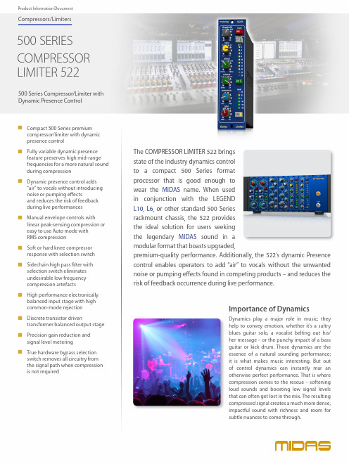
500 Series Compressor/Limiter with Dynamic Presence ControlCOMPRESSOR LIMITER 522##Compact 500 Series premium compressor/limiter with dynamic presence control##Fully variable dynamic presence feature preserves high mid-range frequencies for a more natural sound during compression##Dynamic presence control adds “air” to vocals without introducing noise or pumping effectsand reduces the risk of feedback during live performances##Manual envelope controls with linear peak-sensing compression or easy to use Auto mode with RMS compression##Soft or hard knee compressor response with selection switch ##Sidechain high pass filter with selection switch eliminates undesirable low frequency compression artefacts##High performance electronically balanced input stage with high common-mode rejection##Discrete transistor driventransformer balanced output stage ##Precision gain reduction and signal level metering##True hardware bypass selection switch removes all circuitry from the signal path when compression is not requiredThe COMPRESSOR LIMITER 522 brings state of the industry dynamics control to a compact 500 Series format processor that is good enough to wear the MIDAS name. When used in conjunction with the LEGEND L10, L6, or other standard 500 Series rackmount chassis, the 522 provides the ideal solution for users seeking the legendary MIDAS sound in a modular format that boasts upgraded,premium-quality performance. Additionally, the 522’s dynamic Presence control enables operators to add “air” to vocals without the unwanted noise or pumping effects found in competing products – and reduces the risk of feedback occurrence during live performance.Importance of DynamicsDynamics play a major role in music; they help to convey emotion, whether it’s a sultry blues guitar solo, a vocalist belting out his/her message – or the punchy impact of a bass guitar or kick drum. Those dynamics are the essence of a natural sounding performance; it is what makes music interesting. But out of control dynamics can instantly mar an otherwise perfect performance. That is where compression comes to the rescue – softening loud sounds and boosting low signal levels that can often get lost in the mix. The resulting compressed signal creates a much more dense, impactful sound with richness and room for subtle nuances to come through.500 Series Compressor/Limiter with Dynamic Presence ControlCOMPRESSOR LIMITER 522##Power up mute relays prevent switch on thumps##Premium quality components throughout for a crystal-clear audiophile signal path ##10-Year Warranty Program*##Designed and engineered in the U.K.Manual or Auto ModesWhen operating in its default mode (Auto switch not engaged) the 522 functions as a peak-sensing compressor, providing tight peak control via instantaneous changes in gain reduction, which produces more obvious compression. This allows the operator to manually adjust the compressor attack and release times so that the compressor operates in peak mode with linear attack curves. When the Auto switch is engaged, the manual attack and release controls are bypassed and the compressor operates in RMS mode, automatically adjusting the attack and release based on the averaged input signal andthe threshold/ratio settings. This produces a smooth, more relaxed compression that is perceived as more musical and natural sounding.Variable Dynamics & “Air ”The range of mid-high audio frequencies (centered around 5 kH z) can be boosted to increase the sense of presence of vocals and solo instruments. As 522’s Presence control is adjusted above minimum, those mid-high frequencies are increasingly boosted during compression, allowing a sound or instrument to cut through or seem more present in the mix. This variable presence function enables the 522 to effectively operate with two different ratios, one for low frequencies (LF) and the other for mid-high frequencies (reduced ratio). The primary effects are: heavy compression and dynamic control can be applied withoutsounding unnatural; and the reduced compression in the human ear’s most sensitive range makes the material sound brighter. However, since high frequency (HF) make up gain is not required, unwanted noise, pumping, and howl-round during quiet passages are all greatly reduced.500 Series Compressor/Limiter withDynamic Presence ControlCOMPRESSORLIMITER 522Soft or Hard KneeAnother element that affects how natural the output sounds when compressed is how the signalis addressed at and around the knee, or threshold point. By default the 522 is set to Soft kneecompression (switch out), which tends to sound more natural as it blurs the distinction betweenover and under threshold signals, leaving signals below threshold unaffected, while signals just overthreshold get compressed at greatly reduced ratios. Only at the point where the signal level risessignificantly above the threshold is full-ratio compression applied. This performance is similar to thatof many vintage compressors due to non-linearities in gain reduction. When the Hard knee switchis activated, the 522 operates in a more surgical fashion with a more sharply defined transitionbetween under and over threshold, making it ideal for limiting style compression. In this mode asmall amount of Soft knee is retained to keep the sound reasonably natural.Sidechain HPFCOMPRESSOR LIMITER 522’s Sidechain high pass filter (HPF) switch lets you insert a 200 Hz HPF intothe compressor side chain, which keeps LF signals from dominating overall signal compression –and effectively eliminates the unwanted artefacts and pumping effects on higher frequencies.High Performance Balanced Input StageDecades of experience, paired with the premium-grade components that make up every input stagewe build, ensures the ultimate in signal integrity that is the very foundation of our design process.That warm and organic MIDAS sound has been heard by millions of concert goers – and recordedfor posterity on countless live albums. The input stage of the 522 is second to none with its low noiseperformance, which boasts an enviable Common Mode Rejection Ratio (CMRR) of -70 dB @ 1 kHz.500 Series Compressor/Limiter withDynamic Presence ControlCOMPRESSOR LIMITER 522Transistor Driven Transformer Balanced OutputThe output stage of any audio processor is the most critical when it comes to maintaining signal integrity, so the 522 utilises discrete bipolar transistors for both their low distortion and noise characteristics. To finalise the balanced output, a premium quality transformer is employed in order to minimize distortion and maximize clean headroom. 522’s transformer also provides galvanic isolation and generates a more vintage sound, and becomes saturated at lower frequencies to add colour when driven hard.Precision MeteringThe COMPRESSOR LIMITER 522 provides at-a-glance metering with LED stacks that display Gain Reduction and Level independently of each other. The 6 segment Level meter reads from -30 dBu to +20 dBu in 10 dB steps, while the 10 segment Gain Reduction meter reads from -2 dB to -20 dB in 2 dB steps.True Hardware Bypass & Power Up MuteFor those occasions when compression is not needed, 522’s IN switch can be disengaged to remove all circuitry from the signal path via true hardware relay bypass. Additionally, true bypass mode engages should the chassis become accidentally powered down.500 Series Compressor/Limiter with Dynamic Presence ControlCOMPRESSOR LIMITER 522You Are CoveredWe always strive to provide the best possible Customer Experience. Our products are made in our own MUSIC Tribe factory using state-of-the-art automation, enhanced production workflows and quality assurance labs with the most sophisticated test equipment available in the world. As a result, we have one of the lowest product failure rates in the industry, and we confidently back it up with a generous Warranty program .500 Series Compressor/Limiter with Dynamic Presence ControlCOMPRESSOR LIMITER 522Dimensions155,80[6.1339]146,80[5.7795]3,00[0.1181]37,90[1.4921]132,08[5.2000]500 Series Compressor/Limiter with Dynamic Presence ControlCOMPRESSOR LIMITER 522Technical SpecificationsControlsThreshold -50 dBu to +25 dBu knob Ratio 1:1 to ∞ knob Attack 0.1 ms to 20 ms knob Release 50 ms to 2 seconds knob Presence Minimum to maximum knob Makeup gain0 dB to +18 dB knobHard knee/soft knee S witch Sidechain high pass filter S witch Automatic attack and release S witch Compressor in S witchInput and OutputInput Mono, balanced line OutputMono, balanced via transformerSystemNoise at unity gain -95 dBu (22 Hz - 22 kHz)CMRR, unity gain, 1 kHz -70 dB (typical)Input impedance, 1 kHz 20 kΩFrequency response, unity gain 20 Hz - 20 kHz, +/- 0.5 dBDistortion, unity gain, 1 kHz 0 dBu <0.01% +10 dBu <0.1% +20 dBu<0.5%Maximum input level, 1 kHz +21 dBu Maximum output level, 1 kHz +21 dBu Output impedance, 1 kHz 50 ΩThreshold range -50 dBu to +25 dBu knob Ratio 1:1 to ∞Attack 0.1 ms to 20 ms Release 50 ms to 2 secondsPresenceMinimum (fl at) to maximum (typically -3 dB below the source signal level, during gain reduction)Presence centre frequency 5 kHz, bandwidth typically 4 octaves Make up gain 0 dB to +18 dBGain reduction meter 10 segment, 2 dB to 20 dB in 2 dB steps Output level meter6 segment, -30 dBu to +20 dBu in 10 dB steps Side chain high pass filter200 Hz, 12 dB per octavePower RequirementsVoltage+16 V and -16 V Power consumption130 mA, 4.2 WPhysicalDimensions (H x W x D) 132 x 38 x 174 mm (5.2 x 1.5 x 6.9")Weight0.7 kg (1.5 lbs)500 Series Compressor/Limiter with Dynamic Presence ControlCOMPRESSOR LIMITER 522Architecture & Engineering SpecificationsThe Midas 522 module shall provide a single channel compressor/limiter in a standard format 500 series single width module.The 522 module shall provide a fully variable threshold control with a range of -50 dBu to +25 dBu.The 522 module shall provide a fully variable ratio control with a range of 1:1 to infinity.The 522 module shall provide a fully variable attack control with a range of 0.1 ms to 20 ms.The 522 module shall provide a fully variable release control with a range of 50 ms to 2 s.The 522 module shall provide a fully variable dynamic presence control with a range from a flat response to a maximum of 3 dB below the current input signal level. The presence control shall only provide boost during gain reduction. The presence control shall have a centre frequency of 5 kHz and a bandwidth of typically 4 octaves.The 522 module shall provide a fully variable make up gain control with a range of 0 dB to +18 dB.The 522 module shall provide a hard knee pushbutton switch to select between soft and hard knee compression modes.The 522 module shall provide a side chain high pass filter in pushbutton switch to enable the 200 Hz, 12 dB per octave side chain filter.The 522 module shall provide an auto switch to enable automatic program dependant attack and release.The 522 module shall provide a compressor in pushbutton switch to enable or bypass the compressor/limiter. In the event of power loss true hardware bypass shall be enabled.The 522 module shall provide a 10 segment gain reduction meter with a range from 2 dB to 20 dB in 2 dB steps.The 522 module shall provide a 6 segment output level meter with a range from -30 dB to +20 dB in 10 dB steps.The 522 module shall not provide a compressor link or external key function.The 522 module shall provide power up relays to prevent switch on thumps at the output.The 522 module shall provide an electronically balanced audio input with an impedance of 20 kΩ connected to a standard 500 series rack via the modules 15 pin edge connector.The 522 module shall provide a transformer balanced audio output with an impedance of 50Ω connected to a standard 500 series rack via the modules 15 pin edge connector.The 522 module shall be powered from a standard 500 series rack unit and requires +/- 16 VDC @ 130mA.The 522 module dimensions shall be 132 mm high x 38 mm wide x 174 mm deep (5.2 x 1.5 x 6.9"). The nominal weight shall be 0.7 kg (1.5 lbs).The Compressor/limiter shall be the Midas model 522, and no other alternative shall be acceptable.COMPRESSOR LIMITER 522500 Series Compressor/Limiter withDynamic Presence ControlCOMPRESSOR LIMITER 522500 Series Compressor/Limiter withDynamic Presence Control11 of 12500 Series Compressor/Limiter with Dynamic Presence ControlCOMPRESSORLIMITER 522For service, support or more information contact the MIDAS location nearest you:Europe M USIC Tribe Brands UK Ltd.Tel: +44156 273 2290 Email: C ***********************************************************************USA/Canada M USIC Tribe Commercial NV Inc.Tel: +1 702 800 8290 Email: C***********************************************************************JapanMUSIC Tribe Services JP K.K.Tel: +81 3 6231 0453 Email: C***********************************************************************MUSIC Tribe accepts no liability for any loss which may be suffered by any person who relies either wholly or in part upon any description, photograph, or statement contained herein. Technical specifications, appearances and other information are subject to change without notice. All trademarks are the property of their respective owners. MIDAS, KLARK TEKNIK, LAB GRUPPEN, LAKE, TANNOY, TURBOSOUND, TC ELECTRONIC, TC HELICON, BEHRINGER, BUGERA and COOLAUDIO are trademarks or registered trademarks of MUSIC Tribe Global Brands Ltd. © MUSIC Tribe Global Brands Ltd. 2018 All rights reserved.500 Series Compressor/Limiter with Dynamic Presence ControlCOMPRESSORLIMITER 522。
TMO18448(LR13_SAM_eNB_集成配置)_中-水印

All rights reserved © Alcatel-Lucent 2009Passing on and copying of this document, use and communication of its contents not permitted without written authorization from Alcatel-Lucent中国电信2015年度4G 网络维护技能竞赛1. Safety WarningBoth lethal and dangerous voltages may be present within the products used herein. The user is strongly advised not to wear conductive jewelry while working on the products. Always observe all safety precautions and do not work on the equipment alone.The equipment used during this course may be electrostatic sensitive. Please observe correct anti-static precautions.2. Trade MarksAlcatel-Lucent and MainStreet are trademarks of Alcatel-Lucent.All other trademarks, service marks and logos (“Marks”) are the property of their respective holders, including Alcatel-Lucent. Users are not permitted to use these Marks without the prior consent of Alcatel-Lucent or such third party owning the Mark. The absence of a Mark identifier is not a representation that a particular product or service name is not a Mark.Alcatel-Lucent assumes no responsibility for the accuracy of the information presented herein, which may be subject to change without notice.3. CopyrightThis document contains information that is proprietary to Alcatel-Lucent and may be used for training purposes only. No other use or transmission of all or any part of this document is permitted without Alcatel-Lucent’s written permission, and must include all copyright and other proprietary notices. No other use or transmission of all or any part of its contents may be used, copied, disclosed or conveyed to any party in any manner whatsoever without prior written permission from Alcatel-Lucent.Use or transmission of all or any part of this document in violation of any applicable legislation is hereby expressly prohibited.User obtains no rights in the information or in any product, process, technology or trademark which it includes or describes,and is expressly prohibited from modifying the information or creating derivative works without the express written consent of Alcatel-Lucent.All rights reserved © Alcatel-Lucent 20094. DisclaimerIn no event will Alcatel-Lucent be liable for any direct, indirect, special, incidental or consequential damages, including lost profits, lost business or lost data, resulting from the use of or reliance upon the information, whether or not Alcatel-Lucent has been advised of the possibility of such damages.Mention of non-Alcatel-Lucent products or services is for information purposes only and constitutes neither an endorsement, nor a recommendation.This course is intended to train the student about the overall look, feel, and use of Alcatel-Lucent products. Theinformation contained herein is representational only. In the interest of file size, simplicity, and compatibility and, in some cases, due to contractual limitations, certain compromises have been made and therefore some features are not entirely accurate.Please refer to technical practices supplied by Alcatel-Lucent for current information concerning Alcatel-Lucent equipment and its operation, or contact your nearest Alcatel-Lucent representative for more information.The Alcatel-Lucent products described or used herein are presented for demonstration and training purposes only. Alcatel-Lucent disclaims any warranties in connection with the products as used and described in the courses or the related documentation, whether express, implied, or statutory. Alcatel-Lucent specifically disclaims all implied warranties,including warranties of merchantability, non-infringement and fitness for a particular purpose, or arising from a course of dealing, usage or trade practice.Alcatel-Lucent is not responsible for any failures caused by: server errors, misdirected or redirected transmissions, failed internet connections, interruptions, any computer virus or any other technical defect, whether human or technical in nature5. Governing LawThe products, documentation and information contained herein, as well as these Terms of Use and Legal Notices aregoverned by the laws of France, excluding its conflict of law rules. If any provision of these Terms of Use and Legal Notices, or the application thereof to any person or circumstances, is held invalid for any reason, unenforceable including, but not limited to, the warranty disclaimers and liability limitations, then such provision shall be deemed superseded by a valid, enforceable provision that matches, as closely as possible, the original provision, and the other provisions of these Terms of Use and Legal Notices shall remain in full force and effect.中国电信2015年度4G 网络维护技能竞赛1. 用非自配置方法集成eNodeB1 非自配置方法集成eNodeB2 网元用户配置和采集安全3 执行eNodeB 集成(发现管理器)2. 用自配置方法集成eNodeB1 用自配置方法集成eNodeB2 eNodeB 调测3 网元用户配置和采集安全性4 预配置网元管理器5 自配置策略管理器6 发现管理器3. 用5620 SAM 在线和离线配置eNodeB1 配置eNodeB :在线和离线2 用在线配置做eNodeB 微调3 结合WPS 做eNodeB 离线配置4 激活管理器5 删除RAN 对象4.eNodeB 软件升级和备份与恢复1 eNodeB 软件升级2 eNodeB 备份和恢复5.附录:eNodeB 性能监控中国电信2015年度4G 网络维护技能竞赛欢迎了解5620 SAM eNodeB 集成和配置管理课程目标:●-用自配置方法集成和配置eNodeB ●-用非自配置的方法集成和配置eNodeB ●-软件升级与备份和恢复中国电信2015年度4G 网络维护技能竞赛赛竞能技护维络网G4度年512信电国中赛竞能技护维络网G4度年512信电国中赛竞能技护维络网G4度年512信电国中可以用“发现管理器”(Discovery Manager )来集成eNodeB ,而无需使用自配置过程,即在发现eNodeB 时,不向其推送配置。
iMosflm tutorial

iMosflm Tutorial1. Introduction1.1 BackgroundMOSFLM can process diffraction images from a wide range of detectors and produces, as output, an MTZ file of reflection indices with their intensities and standard deviations (and other parameters). This MTZ file is passed onto other programs of the CCP4 program suite (POINTLESS, SORTMTZ, AIMLESS, CTRUNCATE) for further data reduction.The MOSFLM program was originally written to process data collected on film. It was then modified to process data collected using the image plate detector developed at the EMBL outstation in Hamburg by Jules Hendrix and Arno Lentfer, and the name was changed to ipmosflm. This is the current version of the program, which will also process data from CCD and pixel detectors.1.2 InstallationThe new GUI (iMosflm) is currently available for Windows, Mac OSX and Linux platforms. For details of installation visit/harry/mosflm and follow the link to the iMosflm version ....1.3 DocumentationThere are two distinct sources of documentation for MOSFLM, although neither of these currently makes any reference to the new GUI. At present, this document is the only documentation available for iMosflm.1. The MOSFLM user guide. This is available as a plain text file (mosflm_user_guide.txt) or on the web (www.mrc-/harry/mosflm/) as a PDF or HTML document. It is a very good idea to look through this guide before starting serious data processing with MOSFLM, although you do not need it for this tutorial.2. The "on-line" help. If you type "help" at the "MOSFLM =>" prompt (after starting the program) all possible keywords arelisted, with information on each keyword. This information is stored in an ASCII file (mosflm.hlp) which can also be read (and searched) with an editor. This relies on having the environment variable "CCP4_HELPDIR" set to the directory containing this file. This is also available on the MOSFLM web pages under "keyword synopses"1.4 Aims of the tutorialYour task is to process 84 images, hg_001.mar1600 to hg_084.mar1600, collected on a Mar345 image plate detector at a synchrotron beamline. These are crystals of a small domain (91 amino acids) that have been soaked in a mercury compound, resulting in a dataset with a strong anomalous signal which can easily be used to solve the structure. These images have kindly been provided by Camillo Rosano.2. Overview of iMosflmStart the program by typing "imosflm". After a brief pause, the following window will appear:The basic operations listed down the left hand side (Images, Indexing, Strategy, Cell Refinement, Integration, History) can be selected by clicking on the appropriate icon, but those that are not appropriate will be greyed-out and cannot be selected.2.1 Drop Down menusClicking on "Session" will result in a drop-down menu that allows you to save the current session or reload a previously savedsession (or add images):Clicking on "Settings" will allow you to see (and modify) Experiment settings, Processing options and Environment variables. Thesewill be described later.The three small icons below "Session" allow you to start a new session, open a saved session or save the current session. Moving themouse over these icons will result in display of a tooltip describing the action taken if the icon is clicked.3. Adding images to a sessionTo add images to a session, use the "Add images..." icon:Select the correct directory from the pop-up Add Images window (the default is the directory in which iMosflm was launched). All files with an appropriate extension (which can be selected) will be displayed. Double-clicking on any file will result in all images with the same template being added to the session. The template is the whole part of the filename prefix, except the number field which specifies the image number. An alternative is to single-click on one image filename and then click on Open.To open one or several images only, check the 'Selected images only' box and then use click followed by Shift+click to select a range of images or Control+click to select individual image files as required.Loaded images will be displayed in the Images window with the start & end phi values displayed (as read from the image header).All images with the same template belong to the same "Sector" of data.Multiple sectors can be read into the same session. Each sector can have a different crystal orientation.Note that a "Warning" has appeared. Click anywhere on the “1 Warning” text to get a brief description of the warning. In this case it is because the direct beam coordinates stored in the MAR image plate images are not 'trusted' by MOSFLM and the direct beam coordinates have been set to the physical centre of the image. Click on the green tick on the right hand side to dismiss this warning; click anywhere outside the warning box to collapse the box; double-click the warning text itself and more details, hints and notes maybe available from MOSFLM.The direct beam coordinates (read from the image header or set by MOSFLM) and crystal to detector distance are displayed. Thesevalues can be edited if they are not correct.Advanced Usage1. The phi values of images can be edited in the Image window. First click on the Image line to highlight it then click with themouse over the phi values to make them editable allowing new values to be given. These new values are propagated for allfollowing images in the same sector. Starting values for the three missetting angles may also be entered following the imagephi values.2. To delete a sector click on the sector name to select it (it turns blue) then use the right mouse button on the sector to bring upa "delete" button. Move the mouse over the delete button (it turns blue) and click to delete the sector and its images.Individual images can be deleted from the Images pane in the same way.3. If one sector is added and used for indexing, and then a second sector from the same crystal is added, the matrix for thesecond sector will not be defined. To define it, double-click on the matrix name for the first sector, save it to a file, double-click on the matrix name (Unknown) for the new sector and read the matrix file written for the first sector.4. Image DisplayWhen images are added to a session, the first image of the sector is displayed in a separate display window.The "Image" drop-down menu allows display of the previous or next image in the series. The "View" drop-down menu allows the image to be displayed in different sizes (related by scale factors of two), based on the image size and the resolution of the monitor. The line below allows selection of different images, either using right and left arrow or selecting one from the drop-down list of all images in that sector. The image being displayed can also be changed by double-clicking on an image name in the "Images" pane of the main window."+" and "-" will zoom the image without changing the centre. The "Fit image" icon will restore the image to its original size (right mouse button will have the same effect). The "Contrast" icon will give a histogram of pixel values. Use the mouse to drag the vertical dotted line, to the right to lighten the image, to the left to darken it. Try adjusting the contrast.4.1 Display IconsThe eight icons on the left, control the display of the direct beam position, spots found for indexing, bad spots, predicted spots, masked areas, spot-finding search area, resolution limits and display of the active mask for Rigaku detectors respectively.These are followed by icons for Zoom, Pan and Selection tools, and tools for adding spots manually (for indexing), editing masks, circle fitting and erasing spots or masks.Lastly on this toolbar are the entry boxes for h, k & l and a button to search for this hkl among the predicted spots displayed on the image. The button resembles a warning sign if the given hkl cannot be found.4.1.1 Masked areas - circular backstop shadowSelect the masked area icon. A green circle will be displayed showing the default position and size of the backstop shadow.Make sure that the Zoom icon (magnifying glass) is selected and use the left-mouse-button (abbreviated to LMB in following text) to drag out a rectangle around the centre of the image. The inner dotted yellow rectangle will show the part of the image that willactually appear in the zoomed area.Choose the Selection Tool. When placed over the perimeter of the circle, the radius of the circular backstop shadow will be displayed. Use the LMB to drag the circle to increase its diameter to that of the actual shadow on the image. The position of the circle can be adjusted with LMB placed on the cross that appears in the centre of the green circle. Adjust the size and position of the circle so that it matches the shadow.4.1.2 Masked areas - general exclusionsChoose the Masking tool. Any existing masked areas will automatically be displayed. Use LMB to define the four corners of the region to be masked. When the fourth position is given, the masked region will be shaded. This region will be excluded from spot finding and integration. This provides a powerful way of dealing with backstop shadows. To edit an existing mask, choose theSelection tool and use the LMB to drag any of the four vertices to a new position.To delete a mask, choose the Spot and mask eraser tool. Place the mouse anywhere within the shaded masked area, and use LMB todelete the mask. Delete any masks that you have created.4.1.3 Spot search areaSelect the Show spotfinding search area icon. The inner and outer radii for the spot search will be displayed as shown below. If theimages are very weak, the spot finding radius will automatically be reduced, but this provides additional control.Either can be changed by dragging with the LMB. Do not change the radii for these images.Advanced UsageThe red rectangle displays the area used to determine an initial estimate of the background of the image. It is important that this does not overlap significant shadows on the image. It can be shifted laterally or changed in orientation (in 90° steps) by dragging with the LMB.4.1.4 Resolution limitsSelect the Show resolution limits icon. The low and high resolution limits will be displayed. The resolution limits can be changed by dragging the perimeter of the circle with LMB (make sure that the Selection Tool has been chosen). The resolution limits will affect Strategy, Cell refinement and Integration, but not spot finding or indexing. The low resolution is not strictly correct (it falls within thebackstop shadow) but does not need to be changed because spots within the backstop shadow will be rejected.4.1.5 Zooming and PanningFirst select a region of the image to be zoomed with the Zoom tool.Select the Pan tool and pan the displayed area by holding down LMB and moving the mouse. This is rapid on a local machine, but may be slow if run on a remote machine over a network.4.1.6 Circle fittingThe circle fitting tool can be used to determine the direct beam position by fitting a circle to a set of points on a powder diffractionring on the image (typically due to icing) or to fit a circular backstop shadow (although using the masking tool is probably easier).Select the circle fitting tool. Three new icons will appear in the image display area. There are two (feint) ice rings visible on theimage at 3.91Å and 3.67Å. Click with LMB on several positions (6-8) on the outer ring (as it is slightly stronger). Then click on thetop circular icon.A circle that best fits the selected points (displayed as yellow crosses) will be drawn, and the direct beam position at the centre of thiscircle will be indicated with a green cross. The direct beam coordinates will be updated to reflect this new position.4.2 Other functionalitiesRight mouse button will return the display to the full size image if it has been zoomed.To get a small zoom window that can be moved over the image, hold down "Shift" with the Zoom tool selected. The area within the dotted square will be zoomed within the solid square.Holding down "Alt" (or "Command" ⌘ on Macs) will display the resolution and the current mouse position on the image in mm and pixels. If positioned over a found spot, the spot coordinates and I/σ(I) will be given. If positioned over a predicted spot position the hkl indices will be shown.5. Spot finding, indexing and mosaicity estimationWhen images have been added, the "Indexing" operation becomes accessible (it is no longer greyed-out).Click on Indexing. This will bring up the major Indexing window in place of the Images window.5.1 Spot FindingBy default, two images 90 degrees apart in phi (or as close to 90 as possible) will be selected and a spot search carried out on both images.Found spots will be displayed as crosses in the Image Display window (red for those above the intensity threshold, yellow for those below). The intensity threshold normally defaults to 20, but will be automatically reduced to 10 or 5 for weak images. The thresholdis determined by the last image to be processed.Images to be searched for spots can be specified in several ways:1. Simply type in the numbers of the images (e.g. 1, 84 above).2. Use the "Pick first image" icon (single blue circle).3. Use the "Pick two images ~90 apart" icon (two blue circles) . This is the default behaviour.4. Use the "Select images ..." icon (multiple circles). If selected, all images in the sector are displayed in a drop-down list. Clickon a image to select it, then double-click on the search icon (resembling a target) for that image to run the spot search. The image will move to the top of the list (together with other images that have been searched).Images to be used for indexing can be selected from those that have been searched by clicking on the "Use" button. If this box was previously checked, then clicking will remove this image from those to be used for indexing. It can be added again by clicking the "Select images ..." icon and clicking on the "Use" box.5.1.1 Difficult imagesParameters affecting the spot search can be modified by selecting the "Settings" drop-down window and selecting "Processing options". The resulting new window contains five tabs relating to Spot finding, Indexing, Processing, Advanced refinement and Advanced integration.The Spot finding window allows the Search area, Spot discrimination parameters, Spot size parameters, Minimum spot separation and Maximum peak separation within spots (to deal with split spots) to be reset. It also allows the choice between a local background determination (preferred) and a radial background determination. The local background method also uses an improved procedure for recognising closely spaced spots. The only parameters commonly changed are:1. Minimum spot separation. This should be the size (in mm) of an average spot (not a very strong spot). Change to valuesestimated by manual inspection of spots if there are difficulties due to badly split spots. This separation parameter is very important when spots are very close, but usually the program will determine a suitable value.2. Minimum pixels per spot. Default value 6, but this will be reduced automatically to 4 if spots are very small.3. Local background box size. Reducing this from 50 to (say) 20 can reduce the number of "false" spots found near any sharpshadow on the image.For data collected in-house spots can be quite large and rather weak. In such cases the spot finding can be greatly improved by the following:1. Reduce the spot finding threshold, e.g. to2.2. Increase the minimum number of pixels per spot to 20-40.3. Reduce the spot rms variation to 1.04. Set the minimum spot separation to a sensible value, e.g. 1.5mm5.2 IndexingProviding there are no errors during spot finding, indexing will be carried out automatically after spot finding. If the image selection or indexing parameters are changed, the "Index" button must be used to carry out the indexing.Autoindexing will be carried out by MOSFLM using spots (above the threshold) from the selected images. The threshold is set by MOSFLM but can be changed using the entry box in the toolbar. The list of solutions, sorted by increasing penalty score, will appear in the lower part of the window. The preferred solution will be highlighted in blue. There will usually be a set of solutions with low penalties (0-20) followed by other solutions with significantly higher penalties. The preferred solution is that with the highest symmetry from the group with low penalty values.Note that all these solutions are really the same P1 solution transformed to the 44 characteristic lattices, with latticesymmetry constraints applied. Therefore, if the P1 solution is wrong, then all the others are wrong as well.For solutions with a penalty less than 50, the refined cell parameters ("ref") will be shown. This can be expanded (click on the + sign) to show the "reg" unrefined but regularised cell (symmetry constraints applied) and the "raw" cell (no symmetry constraints applied). The rms deviation (rmsd) or error in predicted spots positions (σ(x,y) in mm) and the rms error in (σ(φ) in degrees) are given for each solution.Usually the penalty will be less than 20 for the correct solution, although it could be higher if there is an error in the direct beam coordinates (or distance/wavelength). The rmsd (error in spot positions) will typically be 0.1-0.2mm for a correct solution, but if the spots are split or very elongated it can be as high as 1mm or higher.The predicted spot positions for the highlighted solution will be shown on the image display with the following default colour codes: Blue:Fully recorded reflectionYellow:Partially recorded reflectionRed:Spatially overlapped reflection... these will NOT be integratedGreen:Reflection width too large (more than 5 degrees)... not integrated.These colours may be adjusted via the "Tools - Colour predictions" item in the Image display window.Providing there are no errors in the indexing, MOSFLM will automatically estimate the mosaic spread (mosaicity) based on thepreferred solution.Select other solutions with a higher penalty and see how well the predicted patterns match the diffraction image.The rmsd and visual inspection of the predicted pattern are the best ways of checking if a solution is correct. If the agreement is not good, then the autoindexing has probably failed.5.2.1 If the indexing fails - Direct beam searchThe indexing is very sensitive to errors in the direct beam coordinates. For a correct indexing solution, these should be correct to better than half the minimum spot separation. Check, for example, that the current direct beam position is behind the backstop. If there are any ice rings, these can be used to determine the direct beam position (see §4.1.6 Circle fitting).If the accuracy of the direct beam coordinates (generally read from the image header) is uncertain, the program can perform a grid search around the input coordinates. The number and the size of the steps can be set from the Indexing tab of the Processing options menu (Settings - Processing options, see §2.1) but defaults to two steps of 0.5mm on each side of the input coordinates. The direct beam search is started by clicking on the text "Search beam-centre" in the Indexing pane. While in progress, it can be stopped by clicking on the same place, the text of which is now "Abort beam-centre".The indexing will be carried out for each set of starting coordinates (Beam x and Beam y in the table which appears) and, if a solution is found, the refined beam coordinates (Beam x ref, Beam y ref), the unit cell parameters of the triclinic solution and the rmsd error in spot coordinates and in phi will be listed. The correct solution will generally be the one with the smallest rms error in spot positions (σ(x,y)). Note that only the triclinic (P1) solution will be listed. To complete the indexing, double-click on the chosen solution, and the full indexing will carried out for these beam coordinates, with the solutions appearing in the upper window. The results of the direct beam search can be hidden (collapsed) by clicking on the [-] symbol next to "Search beam-centre" and recovered by clicking on [+]5.2.2 If the indexing fails - Other parameters.Errors in other physical parameters (wavelength, crystal to detector distance) can also result in failure. All these parameters should be checked.Several parameters used in autoindexing can also be adjusted using entry fields and buttons that appear in the Indexing toolbar.Weak images1. MOSFLM automatically reduces the I/σ(I) threshold for weak images and it may also reduce the resolution to 4Å but lowervalues can be tried. It is important not to include spots that are not "real" - a small number of false spots can prevent theindexing from working.2. Try changing parameters for spot finding (see 5.1.1)Multiple lattices1. Try increasing the I/σ(I) threshold (default 20), for example to 40 or 60, so that only spots from the stronger lattice are selected.This can be done by entering a new value in the leftmost of the circled icons above (and also via the using the Indexing tab of Processing options).All cases1. Include more images in the indexing.2. In case the crystal orientation has changed, try indexing using only one image.3. If there are ice rings/spots, use the 'Exclude any spot rings during indexing' button.4. If the cell parameters are known, reduce the maximum allowed cell edge to the known maximum cell edge. This can sometimeshelp filter incorrect solutions.5. If the detector distance is uncertain, and the images are high resolution (e.g. 2Å), allow the detector distance to refine duringcell refinement.5.2.2 Space group selectionNote that the indexing is based solely on information about the unit cell parameters. It will therefore be very difficult (or impossible) to determine the correct Laue group in the presence of pseudosymmetry. For example, a monoclinic space group with β ~ 90 will appear to be orthorhombic; an orthorhombic space group with very similar a and b cell parameters will appear to be tetragonal. These can only be distinguished when intensities are available (i.e. after integration) by running POINTLESS.In addition, it is not possible to distinguish between Laue Groups 4/m and 4/mmm, 3 and 3/m, 6/m and 6/mmm, m3 and m3m. This will not affect integration of the images, but it will affect the strategy calculation. In the absence of additional information, the lower symmetry should be chosen to ensure that a complete dataset is collected.The presence of screw axes also cannot be detected, so there is no basis on which to distinguish P21 from P2 etc. This does not affect any aspect of data collection or processing, and can be chosen (on the basis of systematic absences) after integration by running POINTLESS.In this example, there is no way of knowing at this stage if the space group is h3 or h32, so leave it as h3.5.3 Mosaicity estimationThe mosaicity (mosaic spread) will be estimated automatically for the preferredsolution. However, if another solution is chosen, the mosaicity should beestimated again.Click on the "Estimate" button to estimate the mosaicity.A window will appear which plots the total predicted intensity as a function ofmosaic spread, from which an estimate is determined.The predictions displayed on the image will be updated. Entering different valuesof mosaic spread in the box (followed by return) will allow a visual estimate ofthe effect of changing the mosaic spread.The mosaic spread can also be entered in the Images pane by clicking once on theMosaicity line and once again on the value displayed.5.3.1 The mosaic block sizeIn some cases, the apparent mosaic spread is much larger at low resolution than at high resolution, so that if it is set to a value that results in all the low resolution spots being predicted, many more spots are predicted than are visible at high resolution. This effect is best dealt with by adjusting the "Mosaic block size" which is also displayed in the Images pane. This is modelling the size, in microns, of the individual mosaic blocks in the crystal. Decreasing this to values of 0.5-5 microns (say) from the default of 100 microns will result in predicting more spots at low resolution but have virtually no effect at high resolution.6. Saving a sessionThe session can be saved at any time, using the Session drop-down menu referred to in 2.1. The first time that a session is saved, you will be prompted for a filename. The filename convention for saved session files is that the extension is ".mos".Save the current session. Then exit from iMosflm (using the Session drop-down menu), restart iMosflm and read in the saved session. If the program crashes, it should be possible to recover all but the latest actions. Restart iMosflm and it will pop up a "Recover session ..." window.Selecting the Recover button will restore the session as far as possible. This file is written to the directory ".mosflm" in the user's home directory.7. Data collection strategyOnce the crystal orientation and (probable) Laue group have been determined, it is possible to calculate a data collection strategy and the Strategy icon is no longer greyed-out (in fact, all other operations, Strategy, Cell Refinement and Integration become possible at this point).Select the Strategy icon. This will open the Strategy window.The statistics initially presented in the window are based on the assumption that all images between the smallest phi value and the largest phi value in the current sector(s) have been collected (the phi ranges are listed). If processing a dataset that has already been collected (as in this tutorial) this is appropriate.More usually, the Strategy option will be used after two initial images, 90° apart in φ, have been collected. In such cases a complete, shaded segment will not be shown in the lower part of the screen, rather an empty circle will be shown with the matrix label beneath it. In cases where two reference images have been collected and indexed, click the 'Auto-complete' button and, in the pop-up menu that appears, select a rotation angle or 'sweep' of data to collect - or leave the 'Rotation:' setting as 'Auto' for a calculation of maximum completeness for this crystal orientation. Click on Ok and the completeness results will be presented.The orientation of the crystal, expressed as the angles between the a,b,c unit cell axes and the X,Y,Z coordinate frame, is given. X is along the X-ray beam, Z is the rotation axis. A warning will be given if the unique axis is so close to the rotation axis that there will be missing cusp data.7.1 Evaluating completeness manuallyThe completeness of any given segment of data can be determined manually using the circle at the bottom left of the window. Clickon the red segment shown in this circle.。
Imatest史上最详细教程
Imatest史上最详细教程2009 Imatest LLC Imatest Documentation 1 of 451 Imatest Documentation Image Quality An overview of the key image quality factors and how they are measured by Imatest Sharpness - What is it and how is it measured? Introduction - The Slanted-edge test - Calculation details - Results - Interpreting MTF50 SQF - Subjective Quality Factor Introduction - SQF and MTF - Meaning of SQF - Measuring SQF - The SQF equation - CSF - Links Noise in photographic images Introduction - Appearance - Noise measurements - Noise summary - F-stop noise - The mathematics of noise - Links Sharpening - Why standardized sharpening is needed for comparing cameras Standardized sharpening - Examples Sharpness comparisons - for several digital cameras Introduction - Explanation of results - Tables of results - Interpretation of MTF - Some observations - Links Chromatic Aberration - AKA Color fringing Introduction - Measurement - Demosaicing Veiling glare (Lens flare) Introduction - Target - Measurement - Results - ISO 9358 Color correction matrix Introduction - Math - Multicharts ISO Sensitivity and Exposure Index Introduction - Modules - Equations - RAW files - Related documents Shannon information capacity - information that can pass through a channel without error Meaning - Results - Summary Blur units, MTF, and DXO Analyzer's BxU The Imatest Test Lab - How to build a testing lab Introduction - Hardware - Lighting - Easel - Light measurement - Tripod - Clamps - Putting it together - Targets - Aligning target & camera Imatest Instructions -- General Installation - and getting started Install - Purchase - Register - Offline registration - Files Using Imatest Running Imatest - multi_read - RAW files - Other controls - Pulldown menus - Figures - .CSV and XML output - Use of Imatest RAW files Introduction - Using RAW files - Bayer RAW - dcraw demosaicing - Rawview utility - Generalized Read Raw The Imatest Test Lab - How to build a testing lab Introduction - Hardware - Lighting - Easel - Light measurement - Tripod - Clamps - Putting it together - Targets - Aligning target & camera Troubleshooting - What to do when Imatest doesn't work Installation problems - Problems after install - Missing DLLs - Runtime problems - INI files - Command (DOS) window - Diagnostics runs - Path conflicts Imatest Instructions -- Sharpness modules Using SFR Part 1 - Setting up and photographing SFR targets Slanted-edge test - Print chart - Lighting - Distance - Exposure - Tips - Quality and Distance Using SFR Part 2 - Running Imatest SFR Image file - ROI - Additional input - Equations - Gamma - Warnings - Saving - Repeated runs - Excel CSV output Imatest SFR LCD target Screen Patterns module - Web pattern SFR results: MTF (Sharpness) plot SFR results: - Chromatic Aberration, Noise, and Shannon capacity plot SFR results: Multiple ROI (Region of Interest) plot 2D Summary plot - 1D Summary plot - CSV Output file - Summary explanation - Excel plots Using SFRplus Part 1 - The SFRplus chart: features and how to photograph it Slanted-edge test - Advantages - Obtain chart - Print chart - Lighting - Distance - Exposure - Tips - Quality and Distance Using SFRplus Part 2 - Running Imatest SFRplus Running SFRplus - Rescharts - SFRplus settings windows - Parameters & setup window - Settings & options window - Gamma - Warnings - SFRplus summary Imatest Documentation 2 of 451 Using SFRplus Part 3 - Imatest SFRplus results SFRplus results - Saving - Repeated runs - Excel .CSV (Comma Separated Values) output Using Rescharts - Analysis of resolution-related charts Introduction - Getting started - The Rescharts window - Rescharts modules - Slanted-edge SFR - Log frequency (simple) - Log frequency-contrast Log Frequency - Analysis of log frequency-varying charts Introduction - Photographing, running - Color moire - Output - Pattern - MTF - Comparisons - Calculation details - Nyquist, aliasing Log F-Contrast - Analysis of charts that vary in log frequency andcontrast Introduction - Creating, printing - Photographing, running - Output - Pattern - MTF - MTF/contrast contours - MTFnn Star Chart - Analysis of the Siemens star chart Introduction - Creating, photographing, running - Output - MTF - MTFnn, MTFnnP - MTF contours - Equations MTF Compare - Compare MTFs of different cameras and lenses Introduction - Instructions Batchview - Postprocessor for viewing summaries of SFR, SFRplus results Introduction - Preparation - Instructions How to Test Lenses with SFRplus Introduction - Test chart - Photograph - Run SFRplus - Rescharts SFRplus - SFRplus settings - Interpret the results - Batches - Checklist How to Test Lenses with SFR - (old page: Imatest SFRplus recommended) Introduction - Test target - Photograph - Run SFR - Interpret - Checklist Imatest Instructions -- Tone, color, and spatial modules Using Stepchart Photographing the chart - Running Stepchart - Output - Saving - Dynamic range - Algorithm Stepchart: Applied Image and ISO charts Photographing chart - Instructions - Patch order Dynamic Range - Calculate Dynamic Range from several Stepchart images Introduction - Operation - Results - Dynamic Range bkgnd Using Colorcheck What Colorcheck does - Colorchecker colors - Photographing target - Photographing target - Colorchecker reference sources - Output - Saving - Links Colorcheck Appendix - Algorithms and reference formulas Color error formulas - Algorithm - Grayscale and exposure Using Multicharts - Interactive analysis of several test charts Introduction - Getting started - Reference files - The Multicharts window - Displays and options Multicharts Special Charts - Additional charts, including circles arranged on a square Instructions - Patch numbering - Examples Color correction matrix Introduction - Math - Multicharts Using Uniformity (Light Falloff) - Measures light falloff (lens vignetting) and sensor nonuniformity Instructions - Results Uniformity (Light Falloff): Imatest Master - Instructions for Imatest Master Input dialog box - Hot and dead pixels - Color shading - Uniformity profiles - Polynomial fit - Histograms - Noise detail - Spot detection Using Distortion Introduction - Instructions - Results - Main figure - Decentering - Corrected image - Intersection figure - Radius correction fig - Links - Algorithm Imatest Instructions -- Miscellaneous modules and utilities Using Test Charts - Creates test charts for high quality inkjet printers Introduction - Bitmap patterns - SVG patterns - Options Using Screen Patterns - Monitor patterns for Light Falloff, SFR, Distortion, and monitor calibration Introduction - Light Falloff - SFR - Distortion - Monitor calibration - Monitor gamma - Zone plate - SMPTE color bars - Slanted edges - Colorchecker- Stepchart - Squares (checkerboard) SVG Test Charts - Scalable Vector Graphics charts for MTF measurements Introduction: m x n squares - Squares and wedges - Operation - Options - Output figure - Printing View/Rename Files - using EXIF data Starting - 1. Select folder - 2. Select files - 3. Rename options - 4. Preview - 5. Rename files Imatest IT/EXE instructions - Running Imatest IT (Industrial Testing)/EXE Introduction - Installation - Setup - INI files - DOS call - Calling from Matlab - Testing - Error handling Using Print Test - Measure print quality factors: color response, tonal response, and Dmax Introduction - Instructions - Results Maskfill - Removes features that interfere with Imatest measurements Imatest Documentation 3 of 451 Introduction - Instructions Appendix Cross-reference tables - Tables to help you navigate Imatest Suppliers - Image quality factors - Image quality factors - Modules - Test charts - Test images Version comparisons - Differences between versions. Which is right for you? Glossary Glosario en Espanol Troubleshooting - What to do when Imatest doesn't work Installation problems - Problems after install - Missing DLLs - Runtime problems - INI files - Command (DOS) window - Diagnostics runs - Path conflicts Imatest Change Log - Imatest release history XML Changes - New XML improvements in Imatest 3.5.1+ Complete PDF documentation - Thewhole docs 14 MB and almost 500 pages, updated occasionally License - The Imatest End User License Agreement (EULA) Imatest Documentation 4 of 451 Image Quality Sharpness What is it and how is it measured? Image sharpness Sharpness is arguably the most important photographic image quality factor: it's the factor most closely related to the amount of detail an image can render. But it's not the only important factor. Imatest measures a great many others. Sharpness is defined by the boundaries between zones of different tones or colors. It is illustrated by the bar pattern of increasing spatial frequency, below. The top portion represents a target used to test a camera/lens combination. It is sharp; its boundaries are abrupt, not gradual. The bottom portion illustrates the effect of a high quality 35mm lens on a 0.5 millimeter long image of the pattern (on the film or digital sensor plane). It is blurred. All lenses, even the finest, blur images to some degree. Poor lenses blur images more than fine ones. One way to measure sharpness is to use the rise distance of the edge, for example, the distance (in pixels, millimeters, or fraction of image height) for the pixel level to go from 10% to 90% of its final value. This is called the 10-90% rise distance. Although rise distance is a good indicator of image sharpness, it has one limitation. It is poorly suited for calculating the sharpness of a complete imaging system from the sharpness of its components, for example, from a lens, digital sensor, and software sharpening algorithm. To get around this problem, measurements are made in frequency domain, where frequency is measured in cycles or line pairs per distance (typically millimeters in film measurements, but may also be inches, pixels, or image height). Line pairs per millimeter (lp/mm) is the most common spatial frequency unit for film, but cycles/pixel is convenient for digital sensors. The image below is a sine wave— a pattern of pure tones— that varies from low to high spatial frequencies, in this case from 2 to 200 lp/mm, over a distance of 0.5 millimeters. The top portion is the original sine pattern. The bottom portion illustrates the effects of the same high quality 35mm lens, which reduces pattern contrast at high spatial frequencies. The relative contrast at a given spatial frequency (output contrast/input contrast) is called the Modulation Transfer Function (MTF) or Spatial Frequency Response (SFR). Illustration of Modulation Transfer Function (MTF) (Spatial frequency response (SFR) ) Imatest Documentation 5 of 451 Green is for geeks. Do you get excited by a good equation? Were you passionate about your college math classes? Then you're probably a math geek—a member of a misunderstood but highly elite fellowship. The text in green is for you. If you're normal or mathematically challenged, you may skip these sections. You'll never know what you missed. The upper plot displays the sine and bar patterns: original and after blurring by the lens. The middle plot displays the luminance of the bar pattern after blurring by the lens (the red curve). Contrast decreases at high spatial frequencies. The lower plot displays the corresponding MTF (SFR) curve (the blue curve). By definition, the low frequency MTF limit is always 1 (100%). For this lens, MTF is 50% at 61 lp/mm and 10% at 183 lp/mm. Both frequency and MTF are displayed on logarithmic scales with exponential notation (10 0 = 1; 10 1 = 10; 10 2 = 100, etc.). Amplitude is displayed on a linear scale. The beauty of using MTF (Spatial Frequency Response) is that the MTF of a complete imaging system is the product of the the MTF of its individual components. MTF is related to edge response by a mathematical operation known as the Fourier transform. MTF is the Fourier transform of the impulse response— the response to a narrow line, which is the derivative (d/dx) of the edge response. Fortunately, you don't need to understand Fourier transforms or calculus to understand MTF. Traditional "resolution" measurements involve observing an image of a bar pattern (usually the USAF 1951 chart) on film, and looking for the highest spatial frequency (in lp/mm) where a pattern is visible. Thiscorresponds to an MTF of about 5-10%. Because this is the spatial frequency where image information disappears—where it isn't visible, it is not a good indicator of image sharpness. Experience has shown that the best indicators of image sharpness are the spatial frequencies where MTF is 50% of its low frequency value (MTF50) or 50% of its peak value (MTF50P). MTF50 or MTF50P are ideal parameters for comparing the sharpness of different cameras for several reasons: (1) Image contrast is half its low frequency or peak values, hence detail is still quite visible. (2) The eye is relatively insensitive to detail at spatial frequencies where MTF is low: 10% or less. (3) The response of virtually all cameras falls off rapidly in the vicinity of MTF50 and MTF50P. MTF50P may better for oversharpened cameras that have peaks in their MTF response. Although MTF can be estimated directly from images of sine patterns (see Rescharts Log Frequency, Log F-Contrast, and Star Chart), a sophisticated technique, based on the ISO 12233 standard, "Photography - Electronic still picture cameras - Resolution measurements," provides more accurate and repeatable results. A slanted-edge image, described below, is photographed, then analyzed by Imatest SFR or Rescharts Slanted-edge SFR. (SFR stands for Spatial Frequency Response.) Origins of Imatest SFR The algorithms for calculating MTF/SFR were adapted from a Matlab program, sfrmat, written by Peter Burns ( ) to implement the ISO 12233 standard. Imatest SFR incorporates numerous improvements, including improved edge detection, better handling of lens distortion, a nicer interface, and far more detailed output. The original Matlab code is available on the I3A ISO tools download page by clicking on ISO 12233 Slant Edge Analysis Tool sfrmat 2.0. In comparing sfrmat 2.0 results with Imatest, note that if no OECF (tonal response curve) file is entered into sfrmat, it assumes that there is no tonal response curve, i.e., gamma = 1. In Imatest, gamma is set to a default value of 0.5, which is typical of digital cameras. To obtain good agreement with sfrmat, you must set gamma to 1. The slanted-edge test for Spatial Frequency Response Slanted-edge test charts can be created with Imatest Test Charts (SVG charts are especially recommended) or downloaded from How to test lenses with Imatest. The bitmap chart has horizontal and vertical edges for best print quality. It should be Imatest Documentation 6 of 451 tilted (about 2-8 degrees) before it is photographed. Imatest SFR can also take advantage of portions of the ISO 12233 test chart, shown on the right, or a derivative like the Applied Image QA-77, or as a less expensive alternative from Danes-Picta in the Czech Republic (the DCR3 chart on their Digital Imaging page)). Two such portions are indicated by the red and blue arrows. ISO 12233 charts are used in and digital camera reviews. A printable vector-graphics version of the ISO chart is available courtesy of Stephen H. Westin of the Cornell University Computer Graphics Department. It should be printed as large as possible (24 inches high if possible) so edge sharpness is not limited by the printer itself. (There may be some jaggedness in the slanted edges; not a problem with the recommended printable target.) A typical portion is shown on the right: a crop of a vertical edge (slanted about 5.6 degrees), used to calculate horizontal MTF response. An advantage of the slanted edge test is that the camera-to-target distance isn't critical. It doesn't enter into the equation that converts the image into MTF response. Imatest Master can calculate MTF for edges of virtually any angle, though exact vertical, horizontal, and 45°can have numerical problems. Slanted edge algorithm (calculation details) The MTF calculation is derived from ISO standard 12233. Some details are contained in Peter Burns' SFRMAT 2.0 User's。
- 1、下载文档前请自行甄别文档内容的完整性,平台不提供额外的编辑、内容补充、找答案等附加服务。
- 2、"仅部分预览"的文档,不可在线预览部分如存在完整性等问题,可反馈申请退款(可完整预览的文档不适用该条件!)。
- 3、如文档侵犯您的权益,请联系客服反馈,我们会尽快为您处理(人工客服工作时间:9:00-18:30)。
A Study of Slanted-Edge MTF Stability and RepeatabilityJackson K.M.RolandImatest LLC,2995Wilderness Place Suite103,Boulder,CO,USAABSTRACTThe slanted-edge method of measuring the spatial frequency response(SFR)as an approximation of the mod-ulation transfer function(MTF)has become a well known and widely used image quality testing method overthe last10years.This method has been adopted by multiple international standards including ISO and IEEE.Nearly every commercially available image quality testing software includes the slanted-edge method and thereare numerous open-source algorithms available.This method is one of the most important image quality algo-rithms in use today.This paper explores test conditions and the impacts they have on the stability and precisionof the slanted-edge method as well as details of the algorithm itself.Real world and simulated data are usedto validate the characteristics of the algorithm.Details of the target such as edge angle and contrast ratio aretested to determine the impact on measurement under various conditions.The original algorithm defines a nearvertical edge so that errors introduced are minor but the theory behind the algorithm requires a perfectly verticaledge.A correction factor is introduced as a way to compensate for this problem.Contrast ratio is shown to haveno impact on results in an absence of noise.Keywords:MTF,SFR,slanted edge,image quality,sharpness1.INTRODUCTIONThe slanted-edge method of measuring the spatial frequency response(SFR)as an approximation of the mod-ulation transfer function(MTF)has become a well known and widely used image quality testing method overthe last10years.This method has been adopted by multiple international standards including ISO and IEEE.1Nearly every commercially available image quality testing software includes the slanted-edge method and thereare numerous open-source algorithms available.This method is easily one of the most important image qualityalgorithms in use today.The algorithm itself has remained relatively unchanged since it’s original publication in ISO12233:2000.2Despite the consistency of the algorithm,in the latest2014revision of the ISO12233standard there was a majormodification to the recommended target.In the original2000edition of ISO12233the target was required tohave a minimum edge contrast of40:1.The revised standard specifies the edge contrast to be4:1.3This changereflects a change in understanding of the slant edge measurement,with high contrast the measurement becomesunstable and so the contrast was lowered.The standard also defines a5 slanted edge rather than another edge angle.There is very little published evidence as to why these specifications are made for the slanted-edgemeasurement.This raises a question,how stable is the slanted-edge method and under what testing conditionswill it be most stable?Mathematically there are several known limitations of the slanted-edge algorithm.First and foremost isthe angle of the the edge being measured relative the the sensor array.The relative edge angle must not beat n⇡4increments where n is an integer value.Should the angle fall on one of these“whole angle”incrementsthe algorithm will be missing frequency information that is calculated from the phase-o↵set portions of an edge relative to the sensor.This paper builds on the work done by Peter Burns4and Don Williams5to help characterize targets and environments.Further author information:(Send correspondence to J.K.M.R)J.K.M.R:E-mail:jackson@,Telephone:+19706928273Table 1:Real-world data set variables Variable Values Edge Angle 5,10,15Contrast Ratio 1.4,2.1,4.3,4.8,11.3,33.7ISO Speed 100,400,1600,64002.EXPERIMENTAL2.1CaptureIn order to validate that simulated edge regions can be used,a data set was acquired from a Canon EOS 6D of a series of slanted edges.The camera was set up on a stable tripod at a distance of 190cm from the targets.The targets were illuminated with 4000K illumination at 355lux with a uniformity of 95%across the measured field.Figure 1:Diagram of lighting setupA series of images was acquired across a range of slanted edge angles,contrast,and noise levels (See Table 1).The contrast level and edge angle was varied by switching out targets.The noise level was varied by changing the ISO sensitivity of the camera.The exposure was kept constant by varying the shutter speed inversely to the ISO sensitivity.The lens model used to capture the data set was a Canon EF 24-70mm f /4L IS USM set to an aperture of f /5.6and a focal length of 70mm.Manual focus was set and maintained for all images captured.The data set was captured in CR2uncompressed raw and large,max quality JPEG formats and for each variable combination 10images were captured.The raw image files were converted to linear TIFF files for processing,removing gamma encoding as a variable.2.2Data ProcessingThe algorithm used to calculate the slanted-edge MTF for all results is a modified version of the ISO standard.The version used here included a noise reduction process on non-edge areas of the region and a second-order fit to the edge instead of a first-order fit.Overall this has reduced the variability present in the results,however the relative di ↵erences remain constant.A follow-up study is planned to show the precise impact of these changes on results.Table 2:Reported slanted-edge resultsMTF50MTF30Light Mean Pixel Value Dark Mean Pixel Value Edge AngleFigure2:Mean MTF plot and edge profile for ISO100,5 Edge Angle,4.3:1Contrast data setA region was selected that would be of a reasonable size and would cover the edge in all images.The metrics shown in Table2were reported along with the MTF curve out to just past the Nyquist frequency and the edge profile(See Figure2).For each reported result the mean and standard deviation was calculated across all10images in each variable set.An example of thefinal reported data is shown in Table3.Table3:Example of results for ISO100,5 Edge Angle,4.3:1Contrast data setResult Mean Std.Dev.MTF500.2300.013MTF300.3170.018Light Mean32.1590.065Dark Mean 6.7400.019Edge Angle 4.6350.0023.SIMULATED DATA GENERATIONIn order to expand the range of testing without having a monumental task of data acquisition,a simulated data set was generated to correlate with the real-world data set.Two simulated data sets were generated:One to match the design of the real-world data set varying similar values and one to cover a much wider range of variables.All data was generated using a MATLAB anti-aliased edge generator which applied an Gaussian-based simulated point spread function(PSF).All noise added to the simulated edges was standard Gaussian noise with a zero-mean and constant variance.Figure3:Example simulated5 edge with no noise(a)MTF50in cycles per pixel plotted as a function of detected edge angle (b)Standard deviation of MTF50plotted as a functionof detected edge angleFigure 4:Plots for real world results4.RESULTS4.1Real World DataThe real world data sets allow us to show the approximate variability under certain circumstances and to estimate the e ↵ect of certain variables when compared to simulated data.The full data set shows some interesting aspects of the camera itself in addition to the more general aspects.Figure 4shows that despite the raw images and lack of signal processing,the camera gave systematically lower results at ISO 1600compared to the higher noise ISO 6400.It also shows that,as might be expected,the highest ISO and likely highest noise had the greatest variability and most outliers.Ignoring the outliers however,the edge angle estimation remains very accurate at all target angles and all noise levels.Furthermore the variability within an noise level remain very similar at all edge angles with no obvious systematic change.Contrast appears to have little e ↵ect on real world data that is outside the variability caused by noise.Edge angle does appear to have an impact on variability in some systems however.At ISO 100the variability of MTF50clearly increases with edge angle.Since this does not seem to occur at any other noise level it is possible that this an artifact of the signal processing in the camera.Further study is needed to determine if this is the case.Figure 5shows the e ↵ect of contrast ratio on the real world data set.Generally the lower contrast ratios have a lower MTF50.This can primarily be expected based on the noise,however an examination of the noise does not fully support this assumption.More study of these results is required and may be discussed in a future paper.Figure 5:MTF50in cycles per pixel plotted as a function of contrast ratio and colored by ISO of the data set with linear trendlinesFigure 6:Simulated contrast data set with varying contrast and constant edge angle4.2ContrastGiven that the contrast ratio change is the only significant change made to standards using the slanted-edge calculation in the last 10years this will be the first issue we look at here.Since these images are completely simulated and there is no radiometric data to associate with the pixel values,it is assumed that these files have a gamma of 1.0.It is also assumed that the simulated values,for the purposes of determining relative contrast of the edge,directly correspond to luminance (Y)values from CIE XYZ (e.g.255pixel =1.0Y).As seen in Figure 7,the MTF50remained extremely stable across all contrast levels with no noise present.The overall standard deviation in the MTF50was less than 0.075%.Statistically speaking,these results are absolutely equivalent.However these measurements were made in an absence of noise.When significant noise is present the contrast does gain certain importance.Figure 8shows the MTF50across the same set of contrast ratios with simulated noise with a sigma of 0.001applied.The lowest contrast (1.1:1)clearly indicates a failed measurement.The addition of the noise was enough to bring the signal to noise ratio so low that the edge was undetectable.Leaving the outlier of the lowest contrast ratio,the remaining contrasts show e ↵ectively the same results as the edges with no noise.The overall standard deviation is higher (2.0%)but this is within the variability created by the noise itself.4.3AngleThe well described theory behind the slanted-edge MTF measurement 6,7explains that the reason behind slanting the edge is to get phase o ↵sets in di ↵erent cross-sections of the same edge.These phase o ↵sets are used to calculated an oversampled edge profile,allowing for detection of frequencies near and above Nyquist.Ideally,the slanted edge would only be slanted enough to pass across a minimum number of sampling sites (pixels)to getFigure 7:MTF50in cycles per pixel across multiple simulated contrast ranges (See Figure 6)Figure8:MTF50in cycles per pixel across multiple simulated contrast ranges with added Gaussian white noise the needed phase o↵set.In practice it is not possible to repeatably capture an image of an edge so close to0 or 90 .The standard most often used became⇠5 so as to allow for variation in the capture while still remaining close to that edge.Figure9:Plot of MTF50values varying with edge angleThere is a problem with this5 angle that has not yet been addressed in any standard or paper.As you move away from perfectly vertical/horizontal,you start to invalidate one of the primary assumptions of the slanted-edge measurement.Specifically the assumption that the edge is in fact perfectly horizontal or vertical. When calculating the edge spread functions(ESF)and line spread function(LSF)the assumption is that the profile is being taken normal to the edge.In a digital sampling system it is di cult to get normal edge profiles for non-sampling-aligned edges without needing to interpolate or otherwise introduce sampling errors.Therefore most algorithms do not attempt this and,assuming that the edge is near aligned to the sampling grid,accept whatever minor errors might be introduced.Figure9is an example of the kind of error this can introduce as you change edge angle.Note the axes,the y-axis has been scaled to emphasize the change occurring.The total di↵erence between1 and44 is37%and the change is clearly systematic,as the edge angle moves closer to 45 from aligned with the sampling grid the lower the MTF gets.Simply put,there is a need to correct the line spread function to account for the rotation.The trigonometric relationship of the corrected line spread width is fairly simply.Figure10shows the geometric relationship and Equation1shows the mathematical relationship.d=l cos(✓)(1) Where l is the width of the line spread function,d is the width of the line spread function normal to the edge,and✓is the angle of the edge relative to the sampling grid.rotated edge profileEquation2shows the mathematical scaling of the LSF.LSF corr(x)=LSF(x cos(✓))(2) Where LSF corr(x)is the corrected line spread function,LSF(x)is the uncorrected line spread function,and x is spatial position on the LSF.With this correction applied the angular di↵erence becomes dramatically smaller(See Figure11)Figure11:Plot of MTF50for uncorrected and corrected measurements The rotation correction improves the results but there is still a slight upward trend in the corrected data. Figure12shows an exaggerated plot of the corrected MTF.The overall di↵erence is only1.6%of the total MTF but the distinctly systematic trend is worth noting.It turns out that when the image has a larger Gaussian PSF applied,the remaining error is reduced.Figure12 also shows the angle set with a wider Gaussian applied to the edges.The axes on Figure12are the same scale but shifted to center on the new data.The mean MTF is much lower,due to the blur,but relative di↵erence angle-to-angle is dramatically lower.The overall di↵erence is now0.23%,an order of magnitude lower than before.The source of this error can be found in the PSFs used.Figure13shows the small Gaussian applied to thefirst data set adjacent to the much larger Gaussian applied to the second.The sampling of the small Gaussian is such that the normally rotationally-invariant Gaussian function has directional factors as you approach45 increments.The larger Gaussian mitigates those factors with denser sampling.This kind of error was introduced by the generation of the simulated data.Real world data will not have the same kind of sampling error and can ignore this factor.Figure12:Corrected MTF and corrected MTF with a smoother PSF appliedFigure13:Gaussian PSFs applied to thefirst and second data set5.CONCLUSIONThe amount of data generated by this study is much too large to cover in a single paper.Significant follow-up studies will be required to fully explore the details,particularly of the real world data.In summary:Simulated data shows that contrast has no e↵ect on MTF unless significant noise is present.In both simulated and real world systems low contrast edges are more susceptible to noise,however there are additional side e↵ects present, possibly related to the camera,that require further study.The core algorithm as defined by ISO12233has significant error as the edge angle deviates from aligned with the sampling grid.If a rotational correction is applied based on the edge angle it is possible to mitigate these e↵ects in real world data.In the simulated data there is additional error related to the sampling of the PSF used to generate the data.In a practical sense this brings up a number of problems related to measuring the image quality of di↵erent cameras.The real world data here shows that even raw data acquired from a camera has processing applied that makes comparison and accurate characterization very di cult.It also highlights the need for automated and controlled environments.Even a relatively well controlled environment that meets the ISO definition of the measurement conditions for resolution had significant variability in certain sets within the remaining uncontrolled variables.If it is not possible to properly characterize a camera without this volume of data acquisition,a much more automated system is necessary.The full real world data set,the MATLAB code for generating slanted edges,and the measured data is available for download from /publications.REFERENCES1.P.CPIQ,“Standard for camera phone image quality,”Institute of Electrical and Electronics Engineers(IEEE),2015.2.ISO/TC42/WG18,“Resolution and spatial frequency response,”International Organization for Standardiza-tion(ISO),2000.3.ISO/TC42/WG18,“Resolution and spatial frequency response,”International Organization for Standardiza-tion(ISO),2014.4.P.D.Burns and D.Williams,“Refined slanted-edge measurement for practical camera and scanner testing,”IS&T PICS Conference,pp.191–195,2002.5.D.Williams and P.D.Burns,“Low-frequency mtf estimation for digital imaging devices using slanted edgeanalysis,”SPIE-IS&T EI Symp.5294,pp.93–101,2004.6.F.Scott,R.M.Scott,and R.V.Shack,“The use of edge gradients in determining modulation-transferfunctions,”Photography Science and Engineering7,pp.64–68,1963.7.R.A.Jones,“An automated technique for deriving mtfs from edge traces,”Photography Science and Engi-neering11,pp.102–106,1967.。