3224W精密贴片电位器
三孔3WL1210型固定安装电路保护器产品说明书
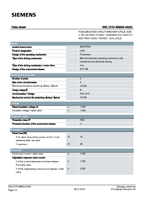
Image database (product images, 2D dimension drawings, 3D models, device circuit diagrams, ...) /bilddb/cax_en.aspx?mlfb=3WL12104BB344AN2
Short-time current resistance (Icw)
● limited to 0.5 s / rated value
kA
● limited to 1 s / rated value
kA
● limited to 2 s / rated value
kA
● limited to 3 s / rated value
2 2
system protection
500
Yes No Yes No
No No
without display
3WL1210-4BB34-4AN2 Page 2/4
05.01.2016
Changes preserved © Copyright Siemens AG
Short circuit
Operational short-circuit current breaking capacity (Ics)
05.01.2016
Changes preserved © Copyright Siemens AG
General Product Approval Shipping Approval
CW1046-DS V1.3 3~4节电池保护IC商品说明书
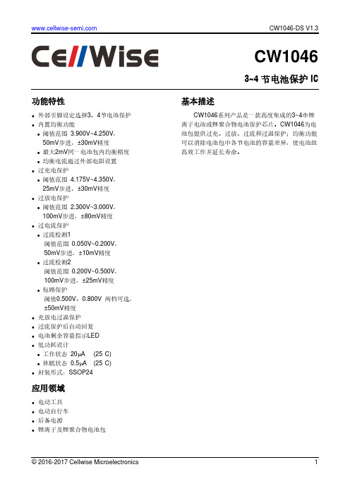
CW1046 3~4节电池保护IC功能特性●外部引脚设定选择3、4节电池保护●内置均衡功能●阈值范围3.900V~4.250V,50mV步进,±30mV精度●最大2mV同一电池包内均衡精度●均衡电流通过外部电阻设置●过充电保护●阈值范围4.175V~4.350V,25mV步进,±30mV精度●过放电保护●阈值范围2.300V~3.000V,100mV步进,±80mV精度●过电流保护●过流检测1阈值范围0.050V~0.200V,50mV步进,±10mV精度●过流检测2阈值范围0.200V~0.500V,100mV步进,±25mV精度●短路保护阈值0.500V、0.800V 两档可选,±50mV精度●充放电过温保护●过流保护后自动回复●电池剩余容量指示LED●低功耗设计●工作状态20μA (25°C)●休眠状态0.5μA (25°C)●封装形式:SSOP24应用领域●电动工具●电动自行车●后备电源●锂离子及锂聚合物电池包基本描述CW1046系列产品是一款高度集成的3~4串锂离子电池或锂聚合物电池保护芯片。
CW1046为电池包提供过充、过放、过流和过温保护;均衡功能可以消除电池包中各节电池的容量差异,使电池组高效工作并延长寿命。
CW1046 典型应用电路*1采样电阻,根据实际需要过流保护值进行调整*2放电高温保护值为75°C,充电高温保护值为55°C,可根据实际需求进行调整,电阻建议选用1%精度*3根据实际均衡电流需求进行调整,但需要注意散热情况CW1046产品选择指南CW1046 X X X X封装形式,S: SSOP24参数类型,从A到Z电池类型,L:代表锂离子电池功能和版本信息,从A 到Z 产品目录CW1046引脚排列图CW10461234567891011121314152423222120191817SEL VC4CB4VC3CB3VC2CB2VC1CB1REG RDOTRCOTLED3LED1VMDO VINICDT CIT CO LED2VSS 16LED4VDDCW1046绝对最大额定值注意:绝对最大额定值是指无论在任何条件下都不能超过的额定值。
3314j电位器参数

3314j电位器参数
3314j是一种电位器型号,通常用于调节电路中的电阻值。
它是一种单轴电位器,具有3个引脚,其中两个是固定端,一个是可变端。
3314j电位器的参数包括阻值范围、公差、功率额定值和温度系数等。
首先,阻值范围是指电位器可调节的电阻数值范围,通常以欧姆(Ω)为单位。
3314j电位器的阻值范围可能在几十欧姆至几兆欧姆之间,具体取决于型号和规格。
其次,公差是指电位器实际阻值与标称阻值之间的允许偏差范围。
一般来说,公差越小,电位器的精度越高。
3314j电位器的公差通常以百分比或者绝对值表示,例如5%的公差表示实际阻值可能偏离标称阻值的5%。
第三,功率额定值是指电位器能够承受的最大功率。
3314j电位器的功率额定值可能在几瓦特到几十瓦特之间,具体取决于型号和尺寸。
最后,温度系数是指电位器阻值随温度变化的稳定性。
温度系
数通常以ppm/℃(百万分之一/摄氏度)来表示,例如50ppm/℃表示在温度每上升1摄氏度时,阻值会上升50百万分之一。
较低的温度系数意味着电位器对温度变化的影响较小。
总的来说,3314j电位器的参数包括阻值范围、公差、功率额定值和温度系数,这些参数决定了它在电路中的具体应用和性能表现。
希望这些信息能够帮助到你。
爱普生SG3225EAN晶体振荡器(SPXO)规格书
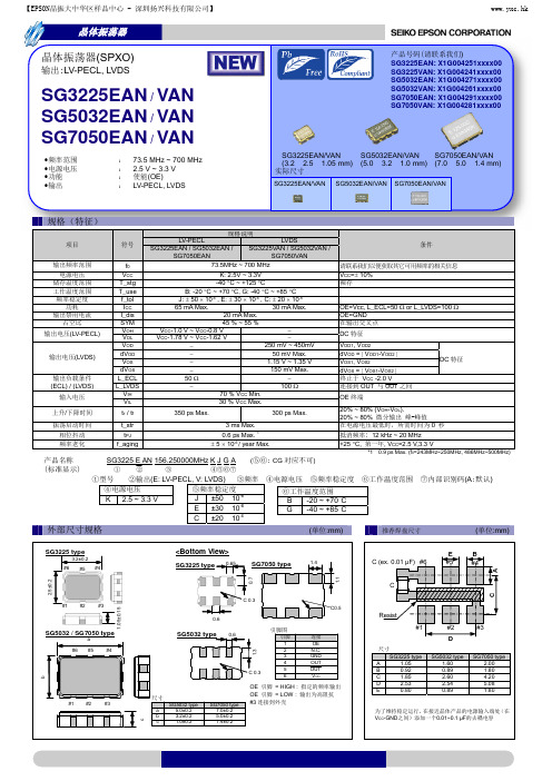
关于在目录内使用的记号
●无铅。 ●符合欧盟 RoHS 指令。 欧盟 RoHS 指令免检的含铅产品。 (密封玻璃、高温熔化性焊料或其他材料中包含铅。 ) ●为汽车方面的应用,如汽车多媒体、车身电子、遥控无钥门锁等。
。 ●为汽车行驶安全方面的应用(引擎控制单元、气囊、电子稳定程序控制系统)
注意事项
·本材料如有变更,恕不另行通知。量产设计时请确认最新信息。 ·未经 Seiko Epson 公司书面授权,禁止以任何形式或任何方式复制或者发布本材料中任何部分的信息内容。 ·本材料中的书面信息、应用电路、编程、使用等内容仅供参考。Seiko Epson 公司对第三方专利或版权的侵权行为不负有任何责任。本材料 未对任何专利或知识版权的许可权进行授权。 ·本材料中规格表中的数值大小通过数值线上的大小关系表示。 ·当出口此材料中描述的产品或技术时,你应该遵守相应的出口管制法律和法规,并按照这些法律和法规的要求执行。 请不要将产品(以及任何情况下提供任何的技术信息)用于开发或制造大规模杀伤性武器或其他军事用途。还要求,不要将产品提供给任何 将产品用于此类违禁用途的第三方。 ·此类产品是基于在一般电子机械内使用而设计开发的,如将产品应用于需要极高可靠性的特定用途,必须实现得到弊公司的事前许可。若 无许可弊公司将不负任何责任。 1.太空设备(人造卫星、火箭等) 2.运输车辆机器控制装置(汽车、飞机、火车、船舶等) 3.用于维持生命的医疗器械 4.海底中转设备 5.发电站控制机器 6.防灾防盗装置 7.交通设备 8.其他,用于与 1~7 具有同等可靠性的用途。
N322 温度控制器操作手册说明书

TEMPERATURE CONTROLLERN322OPERATING MANUAL - V1.8x HThe N322 is a 2-output digital electronic controller for heating and cooling applications. It is available with NTC thermistor input sensor, Pt100, Pt1000 or J/K/T type thermocouple. Sensor offset correction is provided. The 2 independent outputs can be used as control or alarm. The features of a particular model (input sensor type, sensor range, mains supply, etc.) are identified by the label placed on the controller body.SPECIFICATIONSINPUT SENSOR: The sensor is chosen by the user at the time of purchase and is presented on the upper side of the equipment box. The options are:• Thermistor NTC, 10 k Ω @ 25 °C; Range: -50 to 120 °C (-58 to 248 °F); Accuracy: 0.6 °C (1.1 °F);Maximum error in the interchangeability of original NTC sensors: 0.75 °C (1.35 °F). This error can be eliminated through the offset parameter of the equipment. Note: For the NTC thermistor option, the sensor comes with the equipment. Its operating range is limited to -30 to +105 °C (-222 to +221 °F). It has cable of 3 meters in length, 2 x 0.5 mm², and can be extended up to 200 meters. • Pt100; Range: -50 to 300 °C (-58 to 572 °F); α= 0,00385; 3 wires; Accuracy: 0.7 °C (1.3 °F); according to IEC-751 standards;• Pt1000; Range: -200 to 530 °C (-328 to 986 ºF); α= 0,00385; 3 wires; Accuracy: 0.7 °C (1.3 °F);• Thermocouple type J ; Range: 0 to 600 °C (32 to 1112 °F); Accuracy: 3 °C (5.4 °F); • Thermocouple type K ; Range -50 to 1000°C (-58 to 1832 °F); Accuracy: 3 °C (5.4 °F); • Thermocouple type T ; Range: -50 to 400 °C (-58 to 752 °F); Accuracy: 3 °C (5.4 °F); Thermocouples according to IEC-584 standards. MEASUREMENT RESOLUTION:From -19.9 to 199.9 º with NTC, Pt100 and Pt1000: ..................................................... 0.1 Elsewhere: .................................................................................................................. 1 Note : The equipment keeps its precision all over the range, despite the lack of display resolution in a part of the range does not allow its visualization.OUTPUT1: .................... R elay SPDT; 1 HP 250 Vac / 1/3 HP 125 Vac (16 A Resistive) Optionally: .......................................................................... Pulse, 5 Vdc, 25 mA max. OUTPUT2: ........................................................................... Relay: 3 A / 250 Vac, SPST POWER SUPPLY: ....................... 100~240 Vac (± 10 %) or 24 Vdc/ac (12~30 Vdc/ac) ................................................. Mains frequency: 50~60 Hz. Power consumption: 5 VA DIMENSIONS : ................................................ W idth x Height x Depth: 75 x 33 x 75 mm ....................................................................... P anel cut-out: 70 x 29 mm; Weight: 100 g ENVIRONMENT: ............................... Operating temperature: 0 to 40 °C (32 to 104 °F) ............................................................ S torage temperature: -20 to 60 °C (-4 to 140 °F) .....................................................................................Relative humidity: 20 to 85 % RH Housing: Polycarbonate UL94 V-2. Protection: Front panel: IP65, Box: IP42. Suitable wiring: Up to 4.0 mm².RS-485 digital communication; RTU MODBUS protocol (optional). Serial interface not isolated from input circuitry.Serial interface isolated from input circuitry, except in 24 V powered model.ELECTRICAL WIRINGFig. 1 below shows the controller connections to sensor, mains and outputs.Fig. 1 – N322 terminalsPt100 with 3 conductors : Terminals 11, 12 and 13 must have the same wire resistance for proper cable length compensation. For 2 wire Pt100, short circuit terminals 11 and 13.Recommendations for the installation• Signal wires should be installed in grounded conduits and away from power or contactor wires.• The instrument should have its own power supply wires that should not be sharedwith electrical motors, coils, contactors, etc.• Installing RC filters (47 R and 100 nF, series combination) is strongly recommended at contactor coils or any other inductors.OPERATIONThe controller requires the internal parameters to be configured according to the intended use for the instrument. The parameters are organized in 4 groups or levels: Level FunctionTemperature measurement 1Setpoint Adjustment 2Configuration 3CalibrationUpon power-up, the N322 display shows for 1 second its firmware version. This information is useful when consulting the factory.Then, the temperature measured by the sensor is shown on the display. This is the parameter level 0 (temperature measurement level).1SP1SP2uNT will advance to the next parameter in the level. At the end of the level, the controller returns to the first level (0). Use the and keys to alter a parameter value. Notes : 1key is pressed tonon-volatile memory, retaining its value when the controller is de-energized.2If no keyboard activity is detected for over 20 seconds, the controller saves the current parameter value and returns to the measurement level.Level 1 –Setpoint AdjustmentIn this level only the Setpoint (SP1 and SP2) parameters are available, alternating the names with their respective values. Adjust the desired temperature for each setpoint clicking on the and keys.SP1Set Point 1Temperature adjustment for control OUTPUT 1. SP1 value is limited to the values programmed in SPL and SPk in the programming level (Parameter configuration, level 2).SP2Set Point 2Temperature adjustment for control OUTPUT 2. SP2 value is limited to the values programmed in SPL and SPkLevel 2 – Configuration - Parameters configuration LevelContains the configuration parameters to be defined by the user, according to thesystem’s requirements. Useand keys to set the value. The display alternates the parameter name and respective value.UntTemperatureUnit - Selects display indication for degrees Celsius or Fahrenheit.0 – Temperature in degrees Celsius 1 - Temperature in degrees Fahrenheit typInput Type - Selects the input sensor type to be connected to the controller. Available only for thermocouple models, allowing selection of types J, K and T.0 - Thermocouple type J 1 - Thermocouple type K 2 - Thermocouple type T ofsSensor Offset - Offset value to be added to the measured temperature to compensate sensor error.splSP Low Limit - Lower range for SP1 and SP2. SPL must be programmed with a lower value than spK .spKSP High Limit - Upper range for SP1 and SP2. SPx must be greater than spl .ky1OUTPUT 1 Hysteresis : defines the differential range between the temperature value at which the OUTPUT 1 is turned on and the value at which it is turned off. In degrees.ky2OUTPUT 2 Hysteresis : defines the differential range between the temperature value at which the OUTPUT 2 is turned on and the value at which it is turned off. In degrees.Ac1Control action for OUTPUT 1 :0 Reverse: For heating applications. Outputs turn on whentemperature is lower than SP.1 Direct: For cooling applications. Output turns on whentemperature is above SP. Ac2Action 2 - Control OUTPUT 2 action or Alarm functions: 0 Reverse control action (heating). 1 Direct control action (cooling). 2 Low (minimum) temperature alarm. 3 High (maximum) temperature alarm. 4 Alarm for temperature inside the range 5 Alarm for temperature outside the range. 6 Low temperature alarm with initial blocking. 7 High temperature alarm with initial blocking. 8 Inside range alarm with initial blocking. 9 Outside range alarm with initial blocking.The section Working with the Controller describes how these functions work.(nt Control Control - Associates Setpoints and Outputs.Setpoint 1 is assigned to OUTPUT1 and Setpoint 2 to OUTPUT2 (factory setting).1Setpoint 1 is assigned to OUTPUT2 where as Setpoint 2 is directed to OUTPUT1.of1 Off time 1Off time 1 - Defines the minimum off time for control OUTPUT 1. Once OUTPUT 1 is turned off, it remains so for at least the time programmedin of1. For thermocouple inputs this parameter is not available. This parameter is intended for refrigeration systems where longer compressor life is desired. For heating systems, program of1 to zero. Value in seconds, 0 to 999 s.on1 on time 1On time 1 - Defines the minimum on time for control OUTPUT 1. Once turned on, OUTPUT 1 remains so for at least the time programmed in on1. For thermocouple inputs this parameter is not available. This parameter is intended for refrigeration systems where increased compressor life is desired. For heating systems, program on1 to zero. Value in seconds, 0 to 999 s.dl1 Delay 1Delay 1 - Delay time to start control. Upon power-on, control OUTPUT 1 is kept off until the time programmed in dl1is elapsed. Its usage is intended to prevent multiple compressors to start simultaneously after the turn-on of a system with several controllers. Value in seconds, 0 to 250 s.of2 Off time 2Off time 2 - Defines the minimum off time for control OUTPUT 2. Once OUTPUT 2 is turned off, it remains so for at least the time programmed in of2. For thermocouple inputs this parameter is not available. This parameter is intended for refrigeration systems where increased compressor life is desired. For heating systems, program on2 to zero. Value in seconds, 0 to 999 s.on2 on time 2On time 2 - Defines the minimum on time for control OUTPUT 2. Once turned on, OUTPUT 2 remains so for at least the time programmed in on2. For thermocouple inputs this parameter is not available. This parameter is intended for refrigeration systems where increased compressor life is desired. Value in seconds, 0 to 999 s. For heating systems, program of2 to zero.dl2 Delay 2Delay 2 - Delay time for OUTPUT 2 to turn on relative to OUTPUT 1. This parameter defines a particular working mode, typically used in multiple stage systems, where OUTPUT 2 is allowed to go on only if OUTPUT 1 is already on for at least dL2 seconds. Also, OUTPUT 2 is driven off whenever OUTPUT 1 goes off. dL2=0 disables this function. Value in seconds, 0 to 250 s.Adr Address Address- Controllers with the optional RS485 Modbus RTU communication interface have the Adr parameter at the Configuration level. Set a unique Modbus address for each equipment connected to the network. Address range is from 1 to 247.Level 3 – Calibration levelseconds.Don’t press the andkey a few times until the temperaturepas Password - Enter the correct password to unlock write operations for the parameters in the following levels.[Al Calibration low- Offset value of the input. It adjusts the lower measurement range of the sensor.[Ak Calibration High - Gain calibration. It adjusts the upper measurementrange of the sensor.[JL Cold Junction Offset calibration - This parameter is available onlyfor thermocouple.FA( Factory Calibration - Restores factory calibration parameters. Changefrom 0 to 1 restores the calibration parameters with factory values.Prt Protection- Defines the levels of parameters that will be passwordprotected. See "Configuration Protection" for details.Pa( Password Change- Allows changing the current password to a newone. Values from 1 to 999 are allowed.Sn2 Serial number - First part of the controller electronic serial number.sn1 Serial number - Second part of the controller electronic serial number.sn0 Serial number - Third part of the controller electronic serial number.WORKING WITH THE CONTROLLERMultiple output controllers are suited for controlling multiple stage systems.Other applications require OUTPUT 1 to be the control output and OUTPUT 2 to be thealarm.There are eight distinct alarm functions implemented in OUTPUT 2, selected by theparameter Ac2, described below:2 - Low temperature alarm – OUTPUT 2 is turned on when the measuredtemperature falls below the SP2 value.3 -High temperature alarm – OUTPUT 2 is turned on when the measuredtemperature exceeds the value programmed in SP2.4 - Inside range alarm – OUTPUT 2 is turned on when the measuredtemperature is within the range defined by:(SP1 – SP2) and (SP1 + SP2)5 - Outside range alarm: OUTPUT 2 is turned on when the temperature fallsoutside the range defined by:(SP1 – SP2) and (SP1 + SP2)Functions 6, 7, 8 e 9 are identical to the above ones except that they incorporate the InitialBlocking feature, which inhibits the output if an alarm condition is present at start-up. Thealarm will be unblocked after the process reaches a non-alarm condition for the first time.In a multiple stage application, SP1and SP2are configured to operate at differenttemperatures, creating a progressive sequence for turning on the outputs(compressors) in response to a system demand. The output delays for turning on thecompressors (dL1and dL2) cause the compressors to be turned on one by one,minimizing energy demand.Another usage for multiple output controllers is in systems that require automaticselection between cool and heat action. In these applications, one output is configuredas reverse action (heating) and the other as direct action (refrigeration). The outputstatus led P1 and P2 in the controller panel, signals when the control output in on.CONFIGURATION PROTECTIONA protection system to avoid unwanted changes to the controller parametersis implemented. The level of protection can be selected from partial to full. The followingparameters are part of the protection system:Pas When this parameter is presented, the correct password should be entered toallow changes of parameters in the following levels.Prt Defines the level of parameters that will be password protected:1 - Only calibration level is protected (factory configuration);2 - Calibration and Configuration levels are protected;3 - All levels are protected - calibration, Configuration and setpoints.PA(Parameter for definition of a new password. Since it is located in the calibrationlevel, can only be changed by a user that knows the current password. Validpasswords are in the range 1 to 999.Configuration protection usagePAS parameter is displayed before entering a protected level. If the correct password isentered, parameters in all following levels can be changed. If wrong or no password isentered, parameters in the following levels will be read only.Important notes:1- After five consecutive attempts to enter a wrong password, new tentative will beblocked for the next 10 minutes. If the current valid password is unknown, the masterpassword can be used only to define a new password for the controller.2 - The password for a brand new device is 111.MASTER PASSWORDThe master password allows user to define a new password for the controller, even ifthe current password is unknown. The master password is based in the serial numberof the controller, and calculated as following:[ 1 ] + [ higher digit of SN2 ] + [ higher digit of SN1 ] + [ higher digit of SN0 ]For example the master password for the device with serial number 987123465 is: 1 9 3 6as follows: 1 +sn2= 987; sn1= 123; sn0= 465 = 1 + 9 + 3 + 6How to use the master password:1- Enter the master password value at PaS prompt.2- Go to PA( parameter and enter the new password, which must not be zero (0).3- Now you can use this new password to access all controller parameters with modifyrights.ERROR MESSAGESSensor measurement errors force the controller outputs to be turned off. The cause forthese errors may have origin in a bad connection, sensor defect (cable or element) orsystem temperature outside the sensor working range. The display signs related toWARRANTYWarranty conditions are available on our website /warranty.。
模拟器件lc2mos精密四路单刀双掷开关adg411 adg412 adg413说明书
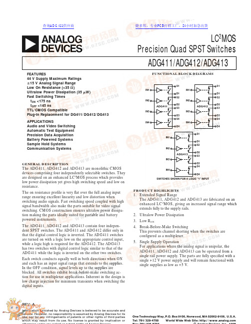
FUNCTIONAL BLOCK DIAGRAMSIN1IN2IN3IN4S1D1S2D2S3D3S4D4ADG411IN1IN2IN3IN4S1D1S2D2S3D3S4D4ADG412IN1IN2IN3IN4S1D1S2D2S3D3S4D4ADG413SWITCHES SHOWN FOR A LOGIC "1" INPUTREV.AInformation furnished by Analog Devices is believed to be accurate and reliable. However, no responsibility is assumed by Analog Devices for its use, nor for any infringements of patents or other rights of third parties which may result from its use. No license is granted by implication oraLC 2MOSPrecision Quad SPST Switches ADG411/ADG412/ADG413One Technology Way, P.O. Box 9106, Norwood, MA 02062-9106, U.S.A.Tel: 781/329-4700World Wide Web Site: FEATURES44 V Supply Maximum Ratings ؎15 V Analog Signal Range Low On Resistance (<35 ⍀)Ultralow Power Dissipation (35 W)Fast Switching Times t ON <175 ns t OFF <145 nsTTL/CMOS CompatiblePlug-In Replacement for DG411/DG412/DG413APPLICATIONSAudio and Video Switching Automatic Test Equipment Precision Data Acquisition Battery Powered Systems Sample Hold Systems Communication SystemsPRODUCT HIGHLIGHTS1.Extended Signal RangeThe ADG411, ADG412 and ADG413 are fabricated on an enhanced LC 2MOS, giving an increased signal range which extends fully to the supply rails.2.Ultralow Power Dissipation 3.Low R ON4.Break-Before-Make SwitchingThis prevents channel shorting when the switches are configured as a multiplexer.5.Single Supply OperationFor applications where the analog signal is unipolar, the ADG411, ADG412 and ADG413 can be operated from a single rail power supply. The parts are fully specified with a single +12 V power supply and will remain functional with single supplies as low as +5 V.GENERAL DESCRIPTIONThe ADG411, ADG412 and ADG413 are monolithic CMOS devices comprising four independently selectable switches. They are designed on an enhanced LC 2MOS process which provides low power dissipation yet gives high switching speed and low on resistance.The on resistance profile is very flat over the full analog input range ensuring excellent linearity and low distortion whenswitching audio signals. Fast switching speed coupled with high signal bandwidth also make the parts suitable for video signal switching. CMOS construction ensures ultralow power dissipa-tion making the parts ideally suited for portable and battery powered instruments.The ADG411, ADG412 and ADG413 contain four indepen-dent SPST switches. The ADG411 and ADG412 differ only in that the digital control logic is inverted. The ADG411 switches are turned on with a logic low on the appropriate control input,while a logic high is required for the ADG412. The ADG413has two switches with digital control logic similar to that of the ADG411 while the logic is inverted on the other two switches.Each switch conducts equally well in both directions when ON and each has an input signal range that extends to the supplies.In the OFF condition, signal levels up to the supplies are blocked. All switches exhibit break-before-make switching ac-tion for use in multiplexer applications. Inherent in the design is low charge injection for minimum transients when switching the digital inputs.查询ADG411供应商捷多邦,专业PCB打样工厂,24小时加急出货ADG411/ADG412/ADG413–SPECIFICATIONS1Dual Supply(V DD = +15 V ؎ 10%, V SS = –15 V ؎ 10%, V L = +5 V ؎ 10%, GND = 0 V, unless otherwise noted)B Version T Version–40؇C to–55؇C toParameter+25؇C+85؇C+25؇C+125؇C Units Test Conditions/Comments ANALOG SWITCHAnalog Signal Range V DD to V SS V DD to V SS VR ON2525Ω typ V D = ±8.5 V, I S = –10 mA;35453545Ω max V DD = +13.5 V, V SS = –13.5 V LEAKAGE CURRENTS V DD = +16.5 V, V SS = –16.5 V Source OFF Leakage I S (OFF)±0.1±0.1nA typ V D = ±15.5 V, V S = ϯ15.5 V;±0.25±5±0.25±20nA max Test Circuit 2Drain OFF Leakage I D (OFF)±0.1±0.1nA typ V D = ±15.5 V, V S = ϯ15.5 V;±0.25±5±0.25±20nA max Test Circuit 2Channel ON Leakage I D, I S (ON)±0.1±0.1nA typ V D = V S = ±15.5 V;±0.4±10±0.4±40nA max Test Circuit 3DIGITAL INPUTSInput High Voltage, V INH 2.4 2.4V minInput Low Voltage, V INL0.80.8V maxInput CurrentI INL or I INH0.0050.005µA typ V IN = V INL or V INH±0.5±0.5µA maxDYNAMIC CHARACTERISTICS2t ON110110ns typ R L = 300 Ω, C L = 35 pF;175175ns max V S = ±10 V; Test Circuit 4t OFF100100ns typ R L = 300 Ω, C L = 35 pF;145145ns max V S = ±10 V; Test Circuit 4 Break-Before-Make Time Delay, t D2525ns typ R L = 300 Ω, C L = 35 pF;(ADG413 Only)V S1 = V S2 = +10 V;Test Circuit 5Charge Injection55pC typ V S = 0 V, R S = 0 Ω, C L = 10 nF;Test Circuit 6OFF Isolation6868dB typ R L = 50 Ω, C L = 5 pF, f = 1 MHz;Test Circuit 7Channel-to-Channel Crosstalk8585dB typ R L = 50 Ω, C L = 5 pF, f = 1 MHz;Test Circuit 8C S (OFF)99pF typ f = 1 MHzC D (OFF)99pF typ f = 1 MHzC D, C S (ON)3535pF typ f = 1 MHzPOWER REQUIREMENTS V DD = +16.5 V, V SS = –16.5 VDigital Inputs = 0 V or 5 VI DD0.00010.0001µA typ1515µA maxI SS0.00010.0001µA typ1515µA maxI L0.00010.0001µA typ1515µA maxNOTES1Temperature ranges are as follows: B Versions: –40°C to +85°C; T Versions: –55°C to +125°C.2Guaranteed by design, not subject to production test.Specifications subject to change without notice.Truth Table (ADG411/ADG412)ADG411 In ADG412 In Switch Condition 01ON10OFF ADG411/ADG412/ADG413Single SupplyB Version T Version–40؇C to–55؇C toParameter+25؇C+85؇C+25؇C+125؇C Units Test Conditions/Comments ANALOG SIGNAL RANGE0 V to V DD0 V to V DD VR ON4040Ω typ0 < V D = 8.5 V, I S = –10 mA;8010080100Ω max V DD = +10.8 VLEAKAGE CURRENTS V DD = +13.2 VSource OFF Leakage I S (OFF)±0.1±0.1nA typ V D = 12.2/1 V, V S = 1/12.2 V;±0.25±5±0.25±20nA max Test Circuit 2Drain OFF Leakage I D (OFF)±0.1±0.1nA typ V D = 12.2/1 V, V S = 1/12.2 V;±0.25±5±0.25±20nA max Test Circuit 2Channel ON Leakage I D, I S (ON)±0.1±0.1nA typ V D = V S = +12.2 V/+1 V;±0.4±10±0.4±40nA max Test Circuit 3DIGITAL INPUTSInput High Voltage, V INH 2.4 2.4V minInput Low Voltage, V INL0.80.8V maxInput CurrentI INL or I INH0.0050.005µA typ V IN = V INL or V INH±0.5±0.5µA maxDYNAMIC CHARACTERISTICS2t ON175175ns typ R L = 300 Ω, C L = 35 pF;250250ns max V S = +8 V; Test Circuit 4t OFF9595ns typ R L = 300 Ω, C L = 35 pF;125125ns max V S = +8 V; Test Circuit 4Break-Before-Make Time Delay, t D2525ns typ R L = 300 Ω, C L = 35 pF;(ADG413 Only)V S1 = V S2 = +10 V;Test Circuit 5Charge Injection2525pC typ V S = 0 V, R S = 0 Ω, C L = 10 nF;Test Circuit 6OFF Isolation6868dB typ R L = 50 Ω, C L = 5 pF, f = 1 MHz;Test Circuit 7Channel-to-Channel Crosstalk8585dB typ R L = 50 Ω, C L = 5 pF, f = 1 MHz;Test Circuit 8C S (OFF)99pF typ f = 1 MHzC D (OFF)99pF typ f = 1 MHzC D, C S (ON)3535pF typ f = 1 MHzPOWER REQUIREMENTS V DD = +13.2 VDigital Inputs = 0 V or 5 VI DD0.00010.0001µA typ1515µA maxI L0.00010.0001µA typ1515µA max V L = +5.25 VNOTES1Temperature ranges are as follows: B Versions: –40°C to +85°C; T Versions: –55°C to +125°C.2Guaranteed by design, not subject to production test.Specifications subject to change without notice.(V DD = +12 V ؎ 10%, V SS = 0 V, V L = +5 V ؎ 10%, GND = 0 V, unless otherwise noted)Truth Table (ADG413)Logic Switch 1, 4Switch 2, 30OFF ON1ON OFFADG411/ADG412/ADG413ORDERING GUIDEModellTemperature Range Package Option 2ADG411BN –40°C to +85°C N-16ADG411BR –40°C to +85°C R-16A ADG411TQ –55°C to +125°C Q-16ADG411BRU –40°C to +85°C RU-16ADG412BN –40°C to +85°C N-16ADG412BR –40°C to +85°C R-16A ADG412TQ –55°C to +125°C Q-16ADG413BN –40°C to +85°C N-16ADG413BR–40°C to +85°CR-16ANOTES 1To order MIL-STD-883, Class B processed parts, add /883B to T grade part numbers.2N = Plastic DIP; R = 0.15" Small Outline IC (SOIC); RU= Thin Shrink Small Outline (TSSOP); Q = Cerdip.ABSOLUTE MAXIMUM RATINGS 1(T A = +25°C unless otherwise noted)V DD to V SS . . . . . . . . . . . . . . . . . . . . . . . . . . . . . . . . . . . .+44 V V DD to GND . . . . . . . . . . . . . . . . . . . . . . . . . .–0.3 V to +25 V V SS to GND . . . . . . . . . . . . . . . . . . . . . . . . . . .+0.3 V to –25 V V L to GND . . . . . . . . . . . . . . . . . . . . . .–0.3 V to V DD + 0.3 V Analog, Digital Inputs 2 . . . . . . . . . . .V SS –2 V to V DD +2 V or30 mA, Whichever Occurs FirstContinuous Current, S or D . . . . . . . . . . . . . . . . . . . . .30 mA Peak Current, S or D . . . . . . . . . . . . . . . . . . . . . . . . . .100 mA (Pulsed at 1 ms, 10% Duty Cycle max)Operating Temperature RangeIndustrial (B Version) . . . . . . . . . . . . . . . . .–40°C to +85°C Extended (T Version) . . . . . . . . . . . . . . . .–55°C to +125°CStorage Temperature Range . . . . . . . . . . . . .–65°C to +150°C Junction Temperature . . . . . . . . . . . . . . . . . . . . . . . . .+150°C Cerdip Package, Power Dissipation . . . . . . . . . . . . . . .900 mW θJA Thermal Impedance . . . . . . . . . . . . . . . . . . . . . .76°C/W Lead Temperature, Soldering (10 sec) . . . . . . . . . . .+300°C Plastic Package, Power Dissipation . . . . . . . . . . . . . . .470 mW θJA Thermal Impedance . . . . . . . . . . . . . . . . . . . . .117°C/W Lead Temperature, Soldering (10 sec) . . . . . . . . . . .+260°C SOIC Package, Power Dissipation . . . . . . . . . . . . . . . .600 mW θJA Thermal Impedance . . . . . . . . . . . . . . . . . . . . . .77°C/W TSSOP Package, Power Dissipation . . . . . . . . . . . . . .450 mW θJA Thermal Impedance . . . . . . . . . . . . . . . . . . . . .115°C/W θJC Thermal Impedance . . . . . . . . . . . . . . . . . . . . . .35°C/W Lead Temperature, SolderingVapor Phase (60 sec) . . . . . . . . . . . . . . . . . . . . . .+215°C Infrared (15 sec) . . . . . . . . . . . . . . . . . . . . . . . . . .+220°CNOTES 1Stresses above those listed under Absolute Maximum Ratings may cause perma-nent damage to the device. This is a stress rating only; functional operation of the device at these or any other conditions above those listed in the operational sections of this specification is not implied. Exposure to absolute maximum rating conditions for extended periods may affect device reliability. Only one absolute maximum rating may be applied at any one time.2Overvoltages at IN, S or D will be clamped by internal diodes. Current should be limited to the maximum ratings given.TERMINOLOGYV DD Most positive power supply potential.V SSMost negative power supply potential in dual supplies. In single supply applications, it may be connected to GND.V L Logic power supply (+5 V).GND Ground (0 V) reference.S Source terminal. May be an input or output.D Drain terminal. May be an input or output.IN Logic control input.R ONOhmic resistance between D and S.I S (OFF)Source leakage current with the switch “OFF.”I D (OFF)Drain leakage current with the switch “OFF.”I D , I S (ON)Channel leakage current with the switch “ON.”V D (V S )Analog voltage on terminals D, S.C S (OFF)“OFF” switch source capacitance.C D (OFF)“OFF” switch drain capacitance.C D , C S (ON)“ON” switch capacitance.t ON Delay between applying the digital control input and the output switching on.t OFF Delay between applying the digital control input and the output switching off.t D“OFF” time or “ON” time measured between the 90% points of both switches, when switching from one address state to another.CrosstalkA measure of unwanted signal which is coupled through from one channel to another as a result of parasitic capacitance.Off Isolation A measure of unwanted signal coupling through an “OFF” switch.Charge A measure of the glitch impulse transferred Injectionfrom the digital input to the analog output during switching.PIN CONFIGURATION(DIP/SOIC)CAUTIONESD (electrostatic discharge) sensitive device. Electrostatic charges as high as 4000V readily accumulate on the human body and test equipment and can discharge without detection.Although the ADG411/ADG412/ADG413 feature proprietary ESD protection circuitry, permanent damage may occur on devices subjected to high energy electrostatic discharges. Therefore, proper ESD precautions are recommended to avoid performance degradation or loss of functionality.ADG411/ADG412/ADG413Typical Performance GraphsFigure 1.On Resistance as a Function of V D (V S ) Dual Supplies Figure 2.On Resistance as a Function of V D (V S ) for Different TemperaturesFigure 3.Leakage Currents as a Function of TemperatureFigure 4.On Resistance as a Function of V D (V S ) Single SupplyFigure 5.Supply Current vs. Input Switching FrequencyFigure 6.Leakage Currents as a Function of V D (V S )ADG411/ADG412/ADG413Figure 7.Off Isolation vs. Frequency Figure 8.Crosstalk vs. Frequency APPLICATIONFigure 9 illustrates a precise, fast, sample-and-hold circuit. An AD845 is used as the input buffer while the output operational amplifier is an AD711. During the track mode, SW1 is closed and the output V OUT follows the input signal V IN. In the hold mode, SW1 is opened and the signal is held by the hold capaci-tor C H.Due to switch and capacitor leakage, the voltage on the hold capacitor will decrease with time. The ADG411/ADG412/ADG413 minimizes this droop due to its low leakage specifica-tions. The droop rate is further minimized by the use of a poly-styrene hold capacitor. The droop rate for the circuit shown is typically 30 µV/µs.A second switch, SW2, which operates in parallel with SW1, is included in this circuit to reduce pedestal error. Since both switches will be at the same potential, they will have a differen-tial effect on the op amp AD711, which will minimize charge injection effects. Pedestal error is also reduced by the compensa-tion network R C and C C. This compensation network also re-duces the hold time glitch while optimizing the acquisition time. Using the illustrated op amps and component values, the pedes-tal error has a maximum value of 5 mV over the ±10 V input range. Both the acquisition and settling times are 850 ns.Figure 9.Fast, Accurate Sample-and-HoldADG411/ADG412/ADG413Test Circuit 1.On ResistanceTest Circuit 3.On LeakageTest CircuitsTest Circuit 2.Off LeakageTest Circuit 4.Switching TimesTest Circuit 5.Break-Before-Make Time DelayTest Circuit 6.Charge InjectionADG411/ADG412/ADG413C 1748a –3–2/98Test Circuit 8.Channel-to-Channel CrosstalkTest Circuit 7.Off Isolation P R I N T E D I N U .S .A .16-Lead Cerdip(Q-16)16-Lead Plastic DIP (Narrow)(N-16)MECHANICAL INFORMATIONDimensions are shown in inches and (mm).16-Lead SOIC (R-16A)16-Lead TSSOP(RU-16)。
Vishay TSM4 5mm方形表面贴装微型调节电位器 使用指南说明书

5 mm Square Surface Mount Miniature Trimmers Multi-TurnCermet SealedDESIGN SUPPORT TOOLSThe TSM4 trimming potentiometer has been designed for surface mount applications and offers volumetric efficiency 5 mm x 5 mm x 3.7 mm with high performance and stability. The TSM4 design is suitable for both manual or automatic operation, and can withstand vapor phase and reflow soldering techniques.FEATURES•0.25 W at 70 °C•Professional and industrial grade•Wide ohmic range (10 Ω to 1 MΩ)•Low contact resistance variation (2 % or 3 Ω)•Small size for optimum packaging density•Tests according to CECC 41000 or IEC 60393-1•Material categorization: for definitions of compliance please see/doc?99912MECHANICAL SPECIFICATIONSMechanical travel13 turns ± 2 Operating torque (max. Ncm)1End stop torque (Ncm)Clutch action (2 turns max.) Unit weight (max. g)0.15Wiper (actual travel)Positioned at approx. 50 %ENVIRONMENTAL SPECIFICATIONSTemperature range-55 °C to +125 °C Climatic category55/125/56 Sealing Sealed container IP67 MSL level1SOLDERING RECOMMENDATIONSRecommended reflow profile 2, see Application Note /doc?52029Note•Nothing stated herein shall be construed as a guarantee of quality or durabilityPERFORMANCESTESTSCONDITIONSTYPICAL VALUES AND DRIFTS∆R T /R T ∆R 1-2/R 1-2OTHERElectrical endurance1000 h at rated power 90'/30' - ambient temp. 70 °C ± 2 %± 3 %Contact res. variation: ∆ < 1 % Rn Climatic sequence Phase A dry heat 125 °C Phase B damp heat Phase C cold -55 °CPhase D damp heat 5 cycles ± 2 %± 3 %Dielectric strength: 600 V RMS Insulation resistance: > 104 M ΩDamp heat, steady state Temperature 40 °C - RH 93 %56 days± 2 %± 3 %Dielectric strength: 600 V RMS Insulation resistance: > 104 M ΩChange of temperature -55 °C to +125 °C5 cycles ± 1 %∆V 1-2/V 1-3 ≤ ± 2 %Mechanical endurance 100 cycles - rated power ± (3 % + 3 Ω)Shock 50 g - 11 ms3 successive shocks in 3 directions± 1 %∆V 1-2/V 1-3 ≤ ± 1 %Vibration10 Hz to 55 Hz 0.75 mm or 10 g - 6 h± 1 %∆V 1-2/V 1-3 ≤ ± 1 %STANDARD RESISTANCE ELEMENT DATASTANDARD RESISTANCE VALUESLINEAR LAWTYPICAL TCR -55 °C +125 °C MAX. POWER AT 70 °CMAX. WORKINGVOLTAGEMAX. CURRENT THROUGH ELEMENTΩW V mA ppm/°C100.25 1.58158± 100200.25 2.23112500.25 3.53771000.25 5.00502000.257.07355000.2511.2221K 0.2515.815.82K 0.2522.311.25K 0.2535.37.110K 0.2550.0 5.020K 0.2570.7 3.550K 0.25112 2.2100K 0.25158 1.6200K 0.25200 1.0500K 0.082000.41M0.042000.2MARKINGVishay trademark, ohmic value, manufacturing dateThe ohmic value is indicated by a 3 figure code, the first two are significant figures, the third one is the multiplier. Example: 100 = 10 Ω101 = 100 Ω 102 = 1000 Ω 503 = 50 000 ΩORDERING INFORMATION (part number)MODEL STYLE OHMIC VALUE TOLERANCE PACKAGING SPECIAL NUMBER TSM4YJ YL ZJ ZLFrom 10 Ω to 1 M Ω504 = 500 k ΩK = 10 %R10 =reel 500 pieces for ZJ and ZLR05 =reel 250 pieces for YJ and YL On request B25 =box of 50 pieces(If applicable)Given by Vishay for custom designDESCRIPTION (for information only)TSM4YL 500K 10 %TR e3MODELSTYLEVALUETOLERANCESPECIALPACKAGINGLEAD (Pb)-FREERELATED DOCUMENTSAPPLICATION NOTES Potentiometers and Trimmers/doc?51001Guidelines for Vishay Sfernice Resistive and Inductive Components/doc?5202955K4RLM4YSTLegal Disclaimer Notice VishayDisclaimerALL PRODU CT, PRODU CT SPECIFICATIONS AND DATA ARE SU BJECT TO CHANGE WITHOU T NOTICE TO IMPROVE RELIABILITY, FUNCTION OR DESIGN OR OTHERWISE.Vishay Intertechnology, Inc., its affiliates, agents, and employees, and all persons acting on its or their behalf (collectively,“Vishay”), disclaim any and all liability for any errors, inaccuracies or incompleteness contained in any datasheet or in any other disclosure relating to any product.Vishay makes no warranty, representation or guarantee regarding the suitability of the products for any particular purpose or the continuing production of any product. To the maximum extent permitted by applicable law, Vishay disclaims (i) any and all liability arising out of the application or use of any product, (ii) any and all liability, including without limitation special, consequential or incidental damages, and (iii) any and all implied warranties, including warranties of fitness for particular purpose, non-infringement and merchantability.Statements regarding the suitability of products for certain types of applications are based on Vishay's knowledge of typical requirements that are often placed on Vishay products in generic applications. Such statements are not binding statements about the suitability of products for a particular application. It is the customer's responsibility to validate that a particular product with the properties described in the product specification is suitable for use in a particular application. Parameters provided in datasheets and / or specifications may vary in different applications and performance may vary over time. All operating parameters, including typical parameters, must be validated for each customer application by the customer's technical experts. Product specifications do not expand or otherwise modify Vishay's terms and conditions of purchase, including but not limited to the warranty expressed therein.Hyperlinks included in this datasheet may direct users to third-party websites. These links are provided as a convenience and for informational purposes only. Inclusion of these hyperlinks does not constitute an endorsement or an approval by Vishay of any of the products, services or opinions of the corporation, organization or individual associated with the third-party website. Vishay disclaims any and all liability and bears no responsibility for the accuracy, legality or content of the third-party website or for that of subsequent links.Except as expressly indicated in writing, Vishay products are not designed for use in medical, life-saving, or life-sustaining applications or for any other application in which the failure of the Vishay product could result in personal injury or death. Customers using or selling Vishay products not expressly indicated for use in such applications do so at their own risk. Please contact authorized Vishay personnel to obtain written terms and conditions regarding products designed for such applications. No license, express or implied, by estoppel or otherwise, to any intellectual property rights is granted by this document or by any conduct of Vishay. Product names and markings noted herein may be trademarks of their respective owners.© 2023 VISHAY INTERTECHNOLOGY, INC. ALL RIGHTS RESERVED。
维科特机电 AM322042H 产品说明书

AM322042H产品说明书在86及110、130混合式步进电机的应用中(主要需求点为900RPM以内,高转矩、高响应、高性价比的定位控制,或者变频调速控制),三相混合式步进电机应用最为广泛。
AM322042H以各行业客户对高压型3相步进电机驱动器的需求为目标(主要针对86及110的电机驱动应用),以行业应用经验为基础,以为客户提供高性价比、高稳定性的产品为宗旨。
整套控制方案在充分吸收和掌握国外先进技术的基础上进行深入优化和提炼而成。
硬件设计上充分考虑强弱电隔离、输入信号兼容、关键物料选用国际知名厂家经典、成熟的元器件;软件上采用改进型的矢量控制技术及其快速算法,并具备自测试运行、单双脉冲模式设置、多重保护等功能。
特点Ø单电源输入,电压范围:交流AC110-240V;Ø驱动电流从有效值1.2A/相到4.2A/相分16档可调;Ø16档细分配置,最高分辨率60000步/转;细分配置小于等于2000步/转时采用微细分控制方式;Ø最高响应频率可达200KHz;Ø相位记忆功能:断电时能自动记忆电机转子位置;Ø保护功能:过热保护/过流保护、相间短路保护、断线保护、过压保护;Ø自动半流:输入脉冲脉冲停止超过100ms时,电流自动减半,减少电机发热;Ø全隔离:信号输入输出隔离;强弱电隔离(pwm控制信号及电流采样均隔离);Ø5V/24V信号输入兼容设计;Ø控制模式可选:脉冲/方向模式;或者双脉冲输入模式;Ø自测试功能:无需外界脉冲信号即可驱动电机以30转/分钟的速度转动;Ø体积为178*109*68 (mm^3),推荐安装空间至少为200*160*90 (mm^3);净重:1kg(加包装箱1.3kg);颜色:白色;Ø采用工业级芯片设计,运行环境温度:-25゜~+60゜(0゜以下不结冰);Ø采用矢量控制及微细分控制技术,在运行平稳性、噪音、震动、发热等方面较传统驱动器均有较大的提升;电流设定驱动器工作电流有效值IM(以下简称IM)由D1-D4拨码开关设定(注:工作电流为正常运行时的电流有效值给定,抱轴时的电流则为对应工作电流的50%,简称自动半流。
GL3224规格书

Genesys Logic, Inc.
12F., No. 205, Sec. 3, Beixin Rd., Xindian Dist. 231, New Taipei City, Taiwan Tel : (886-2) 8913-1888 Fax : (886-2) 6629-6168 http ://
© 2015 Genesys Logic, Inc. - All rights reserved. GLI Confidential
Page 4
GL3224 Datasheet
List of Figures
Figure 3.1 – QFN48 Pinout Diagram ...................................................................................... 9 Figure 3.2 – QFN32 Pinout Diagram .................................................................................... 10 Figure 4.1 – QFN48 Functional Block Diagram .................................................................. 16 Figure 4.2 – QFN32 Functional Block Diagram .................................................................. 16 Figure 5.1 - Timing Diagram of Reset Width ...................................................................... 19 Figure 5.2 - Timing Diagram of Power Good to USB Command Receive Ready ............ 20 Figure 7.1 - QFN 48 Pin Package .......................................................................................... 23 Figure 7.2 - QFN 32 Pin Package .......................................................................................... 24
SP3223中文资料
LOGIC INPUTS AND RECEIVER OUTPUTS
10
µA All RxIN open, ONLINE = GND,
SHUTDOWN = VCC, TxIN=VCC or GND,VCC = +3.3V, TAMB = +25° C
10
µA SHUTDOWN = GND, TxIN=VCC or
SPECIFICATIONS (continued)
Unless otherwise noted, the following specifications apply for VCC = +3.0V to +5.5V with TAMB = TMIN to TMAX. Typical values apply at VCC = +3.3V or +5.0V and TAMB = 25°C.
GND, VCC = +3.3V, TAMB = +25° C
1.0
mA ONLINE = SHUTDOWN = VCC,
no load, VCC = +3.3V, TAMB = +25° C
Input Logic Threshold LOW HIGH
Input Leakage Current
Output Leakage Current
PARAMETER
MIN.
TYP. MAX. UNITS CONDITIONS
DC CHARACTERISTICS
Supply Current,
1.0
AUTO ON-LINE®
Supply Current, Shutdown
1.0
Supply Current,
OPA类TI免费芯片汇集

OPA1013- 精密单电源双路运算放大器OPA1013CN8P 所有无铅库存$0.00OPA124- 低噪声的精密差动运算放大器OPA124U D 所有无铅库存$0.00OPA124UA D 所有无铅库存$0.00OPA129- 超低偏置电流差动运算放大器OPA129U D 所有无铅库存$0.00OPA129UB D 所有无铅库存$0.00OPA131- 通用 FET- 输入运算放大器OPA131UA D 所有无铅库存$0.00OPA1602- OPA1602、OPA1604 SoundPlus 高性能、双极输入音频运算放大器OPA1602AID D 暂时缺货$0.00OPA1642- Sound-Plus 高性能、JFET 输入音频运算放大器OPA1642AID D 暂时缺货$0.00OPA2130- 低功耗精密 FET 输入运算放大器OPA2130UA D 所有无铅库存$0.00OPA2137- 低成本 FET 输入运算放大器OPA2137P P 所有无铅库存$0.00OPA2141- 10MHz 单电源低噪声 JFET 精密放大器 ]]OPA2141AID D 所有无铅库存$0.00OPA2141AIDR D 所有无铅库存$0.00OPA2227- 高精度、低噪声运算放大器OPA2227P P 所有无铅库存$0.00OPA2227U D 所有无铅库存$0.00OPA2227UA D 所有无铅库存$0.00OPA2228- 高精度低噪声运算放大器OPA2228P P 所有无铅/绿色环保库存$0.00OPA2228PA P 所有无铅库存$0.00OPA2228U D 所有无铅库存$0.00OPA2228UA D 所有无铅库存$0.00OPA2333-HT- 1.8V 微功耗 CMOS 运算放大器OPA2333SJD JD 所有无铅无偏好** 库存$0.00OPA2334- 最大漂移0.05uV/℃ 的单电源 CMOS 运算放大器OPA2334AIDGST DGS 所有无铅/绿色环保库存$0.00 OPA2335- 最大漂移0.05uV/℃ 的单电源 CMOS 运算放大器OPA2335AIDGKT DGK 所有无铅库存$0.00 OPA2335AIDR D 所有无铅/绿色环保库存$0.00 OPA2338- MicroSIZE、单电源 CMOS 运算放大器微放大器系列OPA2338EA/250DCN 所有无铅/绿色环保库存$0.00OPA2354- 250MHz 轨至轨 I/O CMOS 双路运算放大器OPA2354AIDDA DDA 所有无铅库存$0.00 OPA2354AIDGKT DGK 所有无铅库存$0.00 OPA2376- 精密、低噪声、低静态电流运算放大器OPA2376AIDR D 所有无铅/绿色环保库存$0.00 OPA2376AIYZDT YZD 所有无铅/绿色环保库存$0.00 OPA2380- 高速精确互阻抗放大器OPA2380AIDGKT DGK 所有无铅/绿色环保库存$0.00 OPA2652- SpeedPlus(TM) 双路 700MHz 电压反馈运算放大器OPA2652U D 所有无铅/绿色环保库存$0.00 OPA2684- 双路低功耗电流反馈运算放大器OPA2684ID D 暂时缺$0.00货OPA2690- 具有禁用功能的双路宽带电压反馈运算放大器OPA2690ID D 所有无铅/绿色环保库存$0.00 OPA2703- 12V CMOS 轨至轨 I/O 运算放大器OPA2703UA D 所有无铅/绿色环保库存$0.00 OPA2703UAG4 D 所有无铅库存$0.00 OPA2704- 12V CMOS 轨至轨 I/O 运算放大器OPA2704EA/250DGK 所有无铅库存$0.00 OPA2704EA/250G4 DGK 所有无铅库存$0.00 OPA2704PA P 所有无铅/绿色环保库存$0.00 OPA2890- 具有禁用功能的双路低功耗宽带电压反馈运算放大器OPA2890ID D 所有无铅/绿色环保库存$0.00 OPA320- 20MHz、0.9pA Ib、RRIO、精密 CMOS 运算放大器OPA320AIDBVT DBV 所有无铅库存$0.00 OPA320SAIDBVT DBV 暂时缺$0.00货OPA3355- 具有关断状态的 2.5V 200MHz 的 GBW CMOS 三路运算放大器OPA3355EA/250PW 所有无铅/绿色环保库存$0.00 OPA3355UA D 所有无铅库存$0.00 OPA337- MicroAmplifier(TM) 系列微型单电源 CMOS 运算放大器OPA337NA/250DBV 所有无铅/绿色环保库存$0.00 OPA343- MicroAmplifier(TM) 系列单电源轨至轨运算放大器OPA343UA D 所有无铅/绿色环保库存$0.00 OPA347- 微功耗轨至轨运算放大器OPA347NA/250DBV 所有无铅/绿色环保库存$0.00 OPA347PA P 所有无铅/绿色环保暂时缺$0.00货OPA347SA/250DCK 所有无铅库存$0.00 OPA353- MicroAmplifier(TM) 系列高速单电源轨至轨运算放大器OPA353UA D 所有无铅/绿色环保库存$0.00 OPA364- 1.8V、高 CMR、RRIO 运算放大器OPA364AID D 所有无铅/绿色环保库存$0.00 OPA364AIDBVT DBV 所有无铅/绿色环保库存$0.00 OPA364IDBVT DBV 所有无铅/绿色环保库存$0.00 OPA3692- 具有禁用功能的三路宽带固定增益缓冲器OPA3692ID D 所有无铅/绿色环保库存$0.00 OPA3692IDBQT DBQ 所有无铅/绿色环保库存$0.00 OPA379- 1.8V、2.9µA、90kHz、轨至轨 I/O 运算放大器OPA379AIDCKT DCK 所有无铅/绿色环保库存$0.00 OPA380- 高速精密互阻抗放大器OPA380AIDGKT DGK 所有无铅库存$0.00 OPA4134- SoundPlus(TM) 高性能音频运算放大器OPA4134UA D 所有无铅库存$0.00 OPA4170- 36V、微功耗、轨至轨输出、四路、通用运算放大器OPA4170AID D 所有无铅库存$0.00 OPA4170AIPW PW 所有无铅库存$0.00 OPA4350- MicroAmplifier(TM) 系列高速单电源轨至轨运算放大器OPA4350EA/250DBQ 所有无铅/绿色环保库存$0.00 OPA4350UA D 所有无铅/绿色环保库存$0.00 OPA4353- MicroAmplifier(TM) 系列高速单电源轨至轨运算放大器OPA4353UA D 所有无铅/绿色环保库存$0.00 OPA4364- 1.8V、高 CMR、RRIO 运算放大器OPA4364AID D 所有无铅/绿色环保库存$0.00 OPA4704- 12V CMOS 轨至轨 I/O 运算放大器OPA4704UA D 所有无铅库存$0.00 OPA548- 高电压大电流运算放大器,出色的输出摆幅OPA548FKTWT KTW 所有无铅/绿色环保库存$0.00 OPA548T KVT 所有无铅/绿色环保库存$0.00 OPA561- 大电流运算放大器OPA561PWP PWP 所有无铅/绿色环保库存$0.00 OPA606- Wide-Bandwidth Difet(R) 运算放大器OPA606KP P 所有无铅/绿色环保库存$0.00 OPA656- 宽带单位增益稳定 FET 输入运算放大器OPA656N/250DBV 所有无铅库存$0.00 OPA656N/250G4DBV 所有无铅库存$0.00 OPA656NB/250DBV 所有无铅库存$0.00 OPA656U D 所有无铅库存$0.00 OPA656UB D 所有无铅库存$0.00 OPA694- 宽带、低功耗、电流反馈放大器OPA694ID D 所有无铅库存$0.00OPA1013- 精密单电源双路运算放大器OPA1013CN8P 所有无铅库存$0.00 OPA121- 低成本的精密差动运算放大器OPA121KU D 所有无铅库存$0.00 OPA124- 低噪声的精密差动运算放大器OPA124U D 所有无铅库存$0.00 OPA124UA D 所有无铅库存$0.00 OPA129- 超低偏置电流差动运算放大器OPA129U D 所有无铅库存$0.00 OPA129UB D 所有无铅库存$0.00 OPA130- 低功耗精密 FET 输入运算放大器OPA130UA D 所有无铅库存$0.00 OPA131- 通用 FET- 输入运算放大器OPA131UA D 所有无铅库存$0.00 OPA132- 高速 FET 输入运算放大器OPA132U D 所有无铅库存$0.00 OPA132UA D 所有无铅库存$0.00 OPA134- SoundPlus(TM) 高性能音频运算放大器OPA134PA P 所有无铅/绿色环保库存$0.00OPA134UA D 所有无铅无偏好** 库存$0.00OPA137- 低成本 FET 输入运算放大器OPA137P P 所有无铅无偏好** 库存$0.00OPA137PA P 库存$0.00 OPA140- 11MHz 单电源、低噪声、精密轨至轨输出 JFET 放大器OPA140AID D 所有无铅库存$0.00 OPA140AIDBVT DBV 所有无铅库存$0.00 OPA140AIDGKT DGK 所有无铅库存$0.00 OPA141- 10MHz 单电源低噪声 JFET 精密放大器OPA141AID D 所有无铅无偏好** 库存$0.00OPA141AIDGKT DGK 所有无铅库存$0.00OPA1602- OPA1602、OPA1604 SoundPlus 高性能、双极输入音频运算放大器OPA1602AID D 暂时缺货$0.00OPA1611- 1.1nV/√Hz 噪声、低功耗精密运算放大器OPA1611AID D 所有无铅库存$0.00OPA1612- 1.1nV/√Hz 噪声、低功耗精密运算放大器OPA1612AID D 所有无铅库存$0.00OPA1632- 全差动 I/O 音频放大器OPA1632D D 所有无铅/绿色环保库存$0.00OPA1632DR D 所有无铅库存$0.00OPA1641- Sound-Plus 高性能、JFET 输入音频运算放大器OPA1641AID D 所有无铅库存$0.00OPA1642- Sound-Plus 高性能、JFET 输入音频运算放大器OPA1642AID D 暂时缺货$0.00OPA1644- OPA1641/1642/1644 SoundPLUS™ 高性能 JFET 输入音频运算放大器OPA1644AID D 所有无铅无偏好** 库存$0.00OPA1654- Sound Plus 低噪声和低失真通用 FET 输入音频运算放大器OPA1654AID D 所有无铅库存$0.00OPA1654AIPW PW 所有无铅库存$0.00OPA1662-Q1- 汽车类 Sound Plus、低功耗、低噪声和低失真音频运算放大器OPA1662AIDGKRQ1 DGK 所有无铅库存$0.00OPA1662AIDRQ1 D 库存$0.00OPA1664- Sound Plus 低功耗、低噪声和低失真音频运算放大器OPA1664AID D 所有无铅库存$0.00OPA1664AIPW PW 所有无铅无偏好** 库存$0.00OPA170- 采用微型封装的 36V、微功耗、轨至轨输出、通用运算放大器OPA170AID D 所有无铅库存$0.00OPA170AIDBVT DBV 所有无铅库存$0.00OPA170AIDRLR DRL 所有无铅库存$0.00OPA170AIDRLT DRL 所有无铅库存$0.00OPA171- 采用微型封装的 36V 通用低功耗 RRO 运算放大器OPA171AID D 所有无铅库存$0.00OPA171AIDBVT DBV 所有无铅库存$0.00OPA171AIDRLT DRL 所有无铅库存$0.00OPA177- 精密运算放大器OPA177FP P 库存$0.00OPA177GP P 所有无铅库存$0.00OPA177GS D 所有无铅库存$0.00OPA177GS/2K5 D 所有无铅库存$0.00OPA188- 0.03μV/°C、6μV Vos、低噪声、轨至轨输出、36V 零漂移运算放大器OPA188AIDGKT DGK 所有无铅库存$0.00OPA1S2385- 具有集成开关和缓冲器的 200-MHz CMOS 跨阻放大器 (TIA)OPA1S2385IDRCT DRC 暂时缺货$0.00OPA211- 1.1nV/(sqrt)Hz Noise, Low Power, Precision Operational Amplifier in DFN-8 Pkg OPA211AIDR D 所有无铅/绿色环保库存$0.00OPA211ID D 所有无铅/绿色环保库存$0.00OPA211IDRGT DRG 所有无铅/绿色环保库存$0.00 OPA2130- 低功耗精密 FET 输入运算放大器OPA2130UA D 所有无铅库存$0.00 OPA2131- 通用 FET 输入运算放大器OPA2131UA D 所有无铅无偏好** 库存$0.00OPA2131UJ D 所有无铅库存$0.00 OPA2132- 高速 FET 输入运算放大器OPA2132P P 库存$0.00OPA2132PA P 所有无铅无偏好** 库存$0.00OPA2132U D 所有无铅无偏好** 库存$0.00OPA2132UA D 所有无铅库存$0.00OPA2134- SoundPlus(TM) 高性能音频运算放大器OPA2134PA P 所有无铅库存$0.00OPA2134UA D 所有无铅库存$0.00OPA2137- 低成本 FET 输入运算放大器OPA2137P P 所有无铅库存$0.00OPA2141- 10MHz 单电源低噪声 JFET 精密放大器 ]]OPA2141AID D 所有无铅库存$0.00OPA2141AIDR D 所有无铅库存$0.00OPA2170- 采用微型封装的 36V、微功耗、轨至轨输出、双路通用运算放大器OPA2170AID D 暂时缺货$0.00OPA2170AIDGK DGK 所有无铅库存$0.00OPA2171- 采用微型封装的 36V 通用低功耗 RRO 运算放大器OPA2171AID D 所有无铅库存$0.00OPA2171AIDCUT DCU 所有无铅库存$0.00OPA2227- 高精度、低噪声运算放大器OPA2227P P 所有无铅库存$0.00OPA2227U D 所有无铅库存$0.00OPA2227UA D 所有无铅库存$0.00OPA2228- 高精度低噪声运算放大器OPA2228P P 所有无铅/绿色环保库存$0.00OPA2228PA P 所有无铅库存$0.00OPA2228U D 所有无铅库存$0.00OPA2228UA D 所有无铅库存$0.00OPA2244- MicroAmplifier(TM) 系列微功耗单电源运算放大器OPA2244EA/250DGK 所有无铅/绿色环保库存$0.00OPA2244PA P 所有无铅库存$0.00OPA2244UA D 所有无铅库存$0.00 OPA2277- 高精度运算放大器OPA2277P P 所有无铅/绿色环保库存$0.00 OPA2277PA P 库存$0.00 OPA2277U D 所有无铅库存$0.00OPA2277UA D 所有无铅无偏好** 库存$0.00OPA2314-EP- 低功耗、低噪声 RRI/O 1.8V CMOS 运算放大器OPA2314ASDRBTEP DRB 库存$0.00 OPA2333- 1.8V、17µA、微功耗、精密、零漂移 CMOS 运算放大器OPA2333AID D 所有无铅/绿色环保库存$0.00 OPA2333AIDGKT DGK 所有无铅库存$0.00 OPA2333AIDRBT DRB 所有无铅/绿色环保库存$0.00 OPA2333-HT- 1.8V 微功耗 CMOS 运算放大器OPA2333SJD JD 所有无铅无偏好** 库存$0.00OPA2334- 最大漂移0.05uV/℃ 的单电源 CMOS 运算放大器OPA2334AIDGST DGS 所有无铅/绿色环保库存$0.00 OPA2335- 最大漂移0.05uV/℃ 的单电源 CMOS 运算放大器OPA2335AIDGKT DGK 所有无铅库存$0.00 OPA2335AIDR D 所有无铅/绿色环保库存$0.00 OPA2336- MicroAmplifier 系列单电源微功耗 CMOS 运算放大器OPA2336E/250DGK 所有无铅库存$0.00 OPA2336PA P 所有无铅库存$0.00 OPA2336U D 所有无铅库存$0.00 OPA2336UA D 所有无铅/绿色环保库存$0.00 OPA2337- MicroSIZE、单电源 CMOS 运算放大器微放大器系列OPA2337UA D 所有无铅/绿色环保库存$0.00 OPA2338- MicroSIZE、单电源 CMOS 运算放大器微放大器系列OPA2338EA/250DCN 所有无铅/绿色环保库存$0.00 OPA2338UA D 所有无铅库存$0.00 OPA2345- MicroAmplifier(TM) 系列低功耗单电源轨至轨运算放大器OPA2345EA/250DGK 所有无铅库存$0.00 OPA2345UA D 所有无铅库存$0.00 OPA2347- 采用 WCSP-8 封装的微功耗轨至轨运算放大器OPA2347EA/250DCN 所有无铅/绿色环保库存$0.00 OPA2347UA D 所有无铅/绿色环保库存$0.00 OPA2347UAG4 D 所有无铅库存$0.00 OPA2354- 250MHz 轨至轨 I/O CMOS 双路运算放大器OPA2354AIDDA DDA 所有无铅库存$0.00 OPA2354AIDGKT DGK 所有无铅库存$0.00 OPA2355- 具有关断状态的 2.5V 200MHz 的 GBW CMOS 双路运算放大器OPA2355DGSA/250 DGS 所有无铅/绿色环保库存$0.00 OPA2356- 2.5V 200MHz 的 GBW CMOS 双路运算放大器OPA2356AID D 所有无铅库存$0.00 OPA2356AIDGKT DGK 所有无铅/绿色环保库存$0.00 OPA2356AIDR D 库存$0.00 OPA237- MicroAmplifier(TM) 系列单电源运算放大器OPA237NA/250DBV 库存$0.00 OPA237NA/3K DBV 暂时缺货$0.00 OPA237UA D 所有无铅库存$0.00 OPA2376- 精密、低噪声、低静态电流运算放大器OPA2376AIDR D 所有无铅/绿色环保库存$0.00 OPA2376AIYZDT YZD 所有无铅/绿色环保库存$0.00 OPA2380- 高速精确互阻抗放大器OPA2380AIDGKT DGK 所有无铅/绿色环保库存$0.00 OPA244- 微功耗单电源运算放大器 MicroAmplifier(TM) 系列OPA244NA/250DBV 所有无铅库存$0.00 OPA244UA D 所有无铅库存$0.00 OPA251- 单电源、微功耗运算放大器OPA251PA P 所有无铅无偏好** 库存$0.00OPA2544- 高电压(大电流)双路运算放大器OPA2544T KV 所有无铅/绿色环保库存$0.00OPA2613- 具有电流限制的双宽带高输出电流运算放大器OPA2613ID D 所有无铅/绿色环保库存$0.00OPA2652- SpeedPlus(TM) 双路 700MHz 电压反馈运算放大器OPA2652U D 所有无铅/绿色环保库存$0.00OPA2673- Dual Wideband High Output Current Operational Amplifier with Current Limit OPA2673IRGVT RGV 所有无铅/绿色环保库存$0.00OPA2684- 双路低功耗电流反馈运算放大器OPA2684ID D 暂时缺货$0.00OPA2690- 具有禁用功能的双路宽带电压反馈运算放大器OPA2690ID D 所有无铅/绿色环保库存$0.00OPA27- 超低噪声精度运算放大器OPA27GP P 所有无铅无偏好** 库存$0.00OPA27GU D 所有无铅库存$0.00 OPA2703- 12V CMOS 轨至轨 I/O 运算放大器OPA2703UA D 所有无铅/绿色环保库存$0.00 OPA2703UAG4 D 所有无铅库存$0.00 OPA2704- 12V CMOS 轨至轨 I/O 运算放大器OPA2704EA/250DGK 所有无铅库存$0.00 OPA2704EA/250G4 DGK 所有无铅库存$0.00 OPA2704PA P 所有无铅/绿色环保库存$0.00 OPA2743- 12V 7MHz 轨至轨 I/O 双路运算放大器OPA2743UA D 所有无铅库存$0.00 OPA2830- 二路、低功耗、单电源宽带运算放大器OPA2830ID D 所有无铅/绿色环保库存$0.00 OPA2830IDGKT DGK 所有无铅/绿色环保库存$0.00 OPA2832- 双通道低功耗高速固定增益运算放大器OPA2832ID D 所有无铅/绿色环保库存$0.00 OPA2832IDGKT DGK 所有无铅/绿色环保库存$0.00 OPA2890- 具有禁用功能的双路低功耗宽带电压反馈运算放大器OPA2890ID D 所有无铅/绿色环保库存$0.00 OPA314- 3MHz、低功耗、低噪声、RRI/O 1.8V CMOS 运算放大器OPA314AIDBVT DBV 库存$0.00OPA320- 20MHz、0.9pA Ib、RRIO、精密 CMOS 运算放大器OPA320AIDBVT DBV 所有无铅库存$0.00OPA320SAIDBVT DBV 暂时缺$0.00货OPA322- 具有关断状态的 20MHz、低噪声、1.8V RRIO、CMOS 运算放大器OPA322AIDBVT DBV 所有无铅库存$0.00OPA330- 1.8V、35µA、微功耗、精密、零漂移 CMOS 运算放大器OPA330AID D 所有无铅库存$0.00OPA330AIDBVT DBV 所有无铅库存$0.00OPA330AIDCKT DCK 所有无铅库存$0.00OPA333- 1.8V、17µA、微功耗、精密、零漂移 CMOS 运算放大器OPA333AIDBVT DBV 所有无铅/绿色环保库存$0.00OPA333AIDCKRG4 DCK 所有无铅库存$0.00OPA333AIDCKT DCK 所有无铅库存$0.00OPA333AIDR D 所有无铅库存$0.00OPA334- 最大漂移0.05uV/℃ 的单电源 CMOS 运算放大器OPA334AIDBVT DBV 所有无铅/绿色环保库存$0.00OPA335- 最大漂移0.05uV/℃ 的单电源 CMOS 运算放大器OPA335AID D 所有无铅库存$0.00OPA335AIDBVT DBV 所有无铅/绿色环保库存$0.00OPA3355- 具有关断状态的 2.5V 200MHz 的 GBW CMOS 三路运算放大器OPA3355EA/250PW 所有无铅/绿色环保库存$0.00OPA3355UA D 所有无铅库存$0.00OPA336- MicroAmplifier(TM) 系列单电源、微功耗 CMOS 运算放大器OPA336N/250DBV 所有无铅/绿色环保库存$0.00OPA336NA/250DBV 所有无铅/绿色环保库存$0.00OPA336NJ/3K DBV 所有无铅库存$0.00OPA336U D 所有无铅/绿色环保库存$0.00 OPA336UA D 所有无铅库存$0.00 OPA337- MicroAmplifier(TM) 系列微型单电源 CMOS 运算放大器OPA337NA/250DBV 所有无铅/绿色环保库存$0.00 OPA340- MicroAmplifier(TM) 系列单电源轨至轨运算放大器OPA340NA/250DBV 库存$0.00 OPA340UA D 所有无铅/绿色环保库存$0.00 OPA342- MicroAmplifier(TM) 系列低成本低功耗轨至轨运算放大器OPA342NA/250DBV 所有无铅/绿色环保库存$0.00 OPA343- MicroAmplifier(TM) 系列单电源轨至轨运算放大器OPA343UA D 所有无铅/绿色环保库存$0.00 OPA344- 低功耗单电源轨至轨运算放大器 MicroAmplifier(TM) 系列OPA344NA/250DBV 所有无铅/绿色环保库存$0.00 OPA344PA P 所有无铅/绿色环保库存$0.00 OPA344UA D 库存$0.00 OPA345- 低功耗单电源轨至轨运算放大器 MicroAmplifier(TM) 系列OPA345NA/250DBV 所有无铅/绿色环保库存$0.00 OPA345UA D 所有无铅/绿色环保库存$0.00 OPA347- 微功耗轨至轨运算放大器OPA347NA/250DBV 所有无铅/绿色环保库存$0.00 OPA347PA P 所有无铅/绿色环保暂时缺货$0.00 OPA347SA/250DCK 所有无铅库存$0.00 OPA348- 1MHz、45uA、RRIO、单路运算放大器OPA348AID D 所有无铅无偏好** 库存$0.00OPA348AIDBVT DBV 所有无铅/绿色环保库存$0.00 OPA348AIDCKT DCK 所有无铅/绿色环保库存$0.00 OPA350- MicroAmplifier(TM) 系列高速单电源轨至轨运算放大器OPA350EA/250DGK 库存$0.00 OPA350PA P 所有无铅库存$0.00 OPA350UA D 所有无铅/绿色环保库存$0.00 OPA353- MicroAmplifier(TM) 系列高速单电源轨至轨运算放大器OPA353NA/250DBV 所有无铅库存$0.00 OPA353UA D 所有无铅/绿色环保库存$0.00 OPA354- 250MHz 轨至轨 I/O CMOS 单路运算放大器OPA354AIDBVT DBV 所有无铅/绿色环保库存$0.00 OPA354AIDDA DDA 所有无铅/绿色环保暂时缺货$0.00 OPA355- 具有关断状态的 2.5V 200MHz 的 GBW CMOS 单路运算放大器OPA355NA/250DBV 所有无铅库存$0.00 OPA355UA D 所有无铅/绿色环保库存$0.00OPA357- 具有关断状态的 250MHz 轨至轨 I/O 单路 CMOS 运算放大器OPA357AIDBVT DBV 所有无铅/绿色环保库存$0.00OPA357AIDDA DDA 所有无铅/绿色环保库存$0.00OPA360- 采用 SC70 封装具有低通滤波器、内部 G=2 和 SAG 校正的 3V 视频放大器OPA360AIDCKT DCK 所有无铅/绿色环保库存$0.00OPA361- 具有内部增益和滤波器的 3V 视频放大器OPA361AIDCKT DCK 所有无铅/绿色环保库存$0.00OPA363- 具有关断状态的 1.8V、高 CMR、RRIO 运算放大器OPA363AID D 所有无铅库存$0.00OPA363AIDBVT DBV 所有无铅/绿色环保库存$0.00OPA363IDBVT DBV 所有无铅/绿色环保库存$0.00OPA364- 1.8V、高 CMR、RRIO 运算放大器OPA364AID D 所有无铅/绿色环保库存$0.00OPA364AIDBVT DBV 所有无铅/绿色环保库存$0.00OPA364IDBVT DBV 所有无铅/绿色环保库存$0.00OPA365- 2.2V、50MHz 低噪声单电源轨至轨运算放大器OPA365AID D 所有无铅/绿色环保库存$0.00OPA365AIDBVT DBV 所有无铅库存$0.00OPA365-EP- 增强型产品 2.2V、50MHz 低噪声单电源轨至轨运算放大器OPA365AMDBVTEP DBV 所有无铅库存$0.00OPA3684- 具有禁用功能的低功耗三路电流反馈运算放大器OPA3684ID D 所有无铅/绿色环保库存$0.00OPA3691- 具有禁用功能的三路宽带电流反馈运算放大器OPA3691ID D 所有无铅/绿色环保库存$0.00OPA3691IDBQT DBQ 所有无铅/绿色环保库存$0.00OPA3692- 具有禁用功能的三路宽带固定增益缓冲器OPA3692ID D 所有无铅/绿色环保库存$0.00OPA3692IDBQT DBQ 所有无铅/绿色环保库存$0.00OPA3693- 具有禁用功能的超宽带电流反馈运算放大器OPA3693IDBQ DBQ 所有无铅/绿色环保库存$0.00OPA3695- 具有禁用功能的超宽带电流反馈运算放大器OPA3695IDBQ DBQ 所有无铅/绿色环保库存$0.00OPA373- 6.5MHz 585uA 轨至轨 I/O CMOS 运算放大器OPA373AIDBVT DBV 所有无铅库存$0.00OPA374- 6.5MHz、585uA、轨至轨 I/O CMOS 运算放大器$0.00OPA374AID D 暂时缺货OPA374AIDBVT DBV 所有无铅/绿色环保库存$0.00OPA376- 低噪声、低 IQ 精密运算放大器OPA376AID D 所有无铅/绿色环保库存$0.00OPA376AIDBVT DBV 所有无铅/绿色环保库存$0.00OPA376AIDCKT DCK 所有无铅/绿色环保库存$0.00OPA378- 低噪声、900kHz、RRIO 零漂移系列的精密运算放大器OPA378AIDBVT DBV 所有无铅库存$0.00 OPA379- 1.8V、2.9µA、90kHz、轨至轨 I/O 运算放大器OPA379AIDCKT DCK 所有无铅/绿色环保库存$0.00 OPA380- 高速精密互阻抗放大器OPA380AIDGKT DGK 所有无铅库存$0.00 OPA381- 精确低功耗高速互阻抗放大器OPA381AIDGKT DGK 所有无铅库存$0.00 OPA3875- OPA3875: Triple 2-to-1 High-Speed Video Multiplexer OPA3875IDBQ DBQ 所有无铅/绿色环保库存$0.00 OPA404- 四路高速精密 Difet(R) 运算放大器OPA404KP N 所有无铅/绿色环保库存$0.00OPA404KU DW 所有无铅无偏好** 库存$0.00OPA4130- 低功耗精密 FET 输入运算放大器OPA4130UA D 所有无铅库存$0.00OPA4131- 通用 FET 输入运算放大器OPA4131NA D 所有无铅库存$0.00OPA4131PA N 所有无铅/绿色环保库存$0.00OPA4131UA DW 所有无铅库存$0.00OPA4132- 高速 FET 输入运算放大器OPA4132UA D 所有无铅库存$0.00OPA4134- SoundPlus(TM) 高性能音频运算放大器OPA4134UA D 所有无铅库存$0.00OPA4137- 低成本 FET 输入运算放大器OPA4137P N 库存$0.00OPA4137U D 所有无铅库存$0.00OPA4137UA D 所有无铅库存$0.00OPA4170- 36V、微功耗、轨至轨输出、四路、通用运算放大器OPA4170AID D 所有无铅库存$0.00OPA4170AIPW PW 所有无铅库存$0.00OPA4171- 36V 通用低功耗 RRO 运算放大器OPA4171AID D 所有无铅库存$0.00OPA4171AIPW PW 所有无铅库存$0.00OPA4180- 0.1 uV/C 漂移、四通道、低噪声、轨到轨、36V 零漂移运算放大器OPA4180ID D 暂时缺货$0.00OPA4180IPW PW 暂时缺货$0.00OPA4209- 2.2nV/rtHz、18MHz、36V RRO 精密运算放大器OPA4209AIPW PW 所有无铅库存$0.00OPA4227- 高精度低噪声运算放大器OPA4227PA N 所有无铅/绿色环保库存$0.00 OPA4227UA D 所有无铅库存$0.00 OPA4228- 高精度低噪声运算放大器OPA4228PA N 所有无铅无偏好** 库存$0.00OPA4228UA D 所有无铅库存$0.00 OPA4234- 低功耗、精密单电源运算放大器OPA4234U D 所有无铅库存$0.00 OPA4241- 单电源、微功耗运算放大器OPA4241UA D 所有无铅库存$0.00 OPA4243- 四路运算放大器,微功耗、单电源OPA4243EA/250PW 所有无铅库存$0.00 OPA4244- MicroAmplifier(TM) 系列微功耗单电源运算放大器OPA4244EA/250PW 所有无铅库存$0.00 OPA4251- 单电源、微功耗运算放大器OPA4251PA N 所有无铅/绿色环保库存$0.00 OPA4251UA D 所有无铅库存$0.00 OPA4277- 高精度运算放大器OPA4277PA N 所有无铅无偏好** 库存$0.00OPA4277UA D 所有无铅库存$0.00OPA4314- 四路、3MHz、低功耗、低噪声、RRI/O、1.8V CMOS 运算放大器OPA4314AIPW PW 所有无铅库存$0.00OPA4317- 四路、低偏移、轨到轨 I/O 运算放大器OPA4317ID D 暂时缺货$0.00OPA4317IPW PW 所有无铅库存$0.00OPA4322- 20MHz、低噪声、1.8V、RRIO、CMOS 运算放大器OPA4322AIPW PW 所有无铅库存$0.00OPA4322SAIPW PW 所有无铅库存$0.00OPA4340- MicroAmplifier(TM) 系列单电源轨至轨运算放大器OPA4340EA/250DBQ 所有无铅/绿色环保库存$0.00OPA4340UA D 所有无铅库存$0.00OPA4343- MicroAmplifier™ 系列单电源轨至轨运算放大器OPA4343NA/250PW 所有无铅/绿色环保库存$0.00OPA4343UA D 所有无铅库存$0.00OPA4344- 低功耗单电源轨至轨运算放大器 MicroAmplifier(TM) 系列OPA4344EA/250PW 所有无铅/绿色环保库存$0.00OPA4344UA D 所有无铅/绿色环保库存$0.00OPA4347- 微功耗轨至轨运算放大器OPA4347UA D 库存$0.00OPA4347UAG4 D 所有无铅暂时缺$0.00货OPA4348- 1MHz、45uA、RRIO、四路运算放大器OPA4348AID D 所有无铅库存$0.00 OPA4348AIPWT PW 所有无铅/绿色环保库存$0.00 OPA4348AIPWTG4 PW 所有无铅库存$0.00 OPA4350- MicroAmplifier(TM) 系列高速单电源轨至轨运算放大器OPA4350EA/250DBQ 所有无铅/绿色环保库存$0.00 OPA4350UA D 所有无铅/绿色环保库存$0.00 OPA4353- MicroAmplifier(TM) 系列高速单电源轨至轨运算放大器OPA4353UA D 所有无铅/绿色环保库存$0.00 OPA4354- 250MHz 轨至轨 I/O CMOS 四路运算放大器OPA4354AIPWT PW 所有无铅库存$0.00 OPA4364- 1.8V、高 CMR、RRIO 运算放大器OPA4364AID D 所有无铅/绿色环保库存$0.00 OPA4376- 精密、低噪声、低静态电流运算放大器OPA4376AIPW PW 所有无铅无偏好** 库存$0.00OPA4377- 低成本、低噪声、5.5MHz CMOS 运算放大器OPA4377AIPW PW 所有无铅库存$0.00 OPA4379- 1.8V、2.5µA、90kHz、轨至轨 I/O 运算放大器OPA4379AIPWR PW 所有无铅/绿色环保库存$0.00 OPA445- 高电压 FET 输入运算放大器OPA445AP P 所有无铅库存$0.00 OPA445AU D 所有无铅库存$0.00 OPA452- 80V 50mA 运算放大器OPA452TA KC 所有无铅库存$0.00 OPA453- 80V 50mA 运算放大器OPA453TA KC 所有无铅库存$0.00 OPA454- 高电压 (100V) 和高电流 (50mA) 运算放大器,G = 1 稳定OPA454AIDDA DDA 所有无铅/绿色环保库存$0.00 OPA4704- 12V CMOS 轨至轨 I/O 运算放大器OPA4704UA D 所有无铅库存$0.00 OPA4743- 12V 7MHz CMOS 轨至轨 I/O 四路运算放大器OPA4743EA/250PW 所有无铅库存$0.00 OPA4820- 四路、单位增益、低噪声、电压反馈运算放大器OPA4820IPWT PW 所有无铅/绿色环保库存$0.00 OPA4830- 低功耗单电源宽带运算放大器OPA4830IPW PW 库存$0.00 OPA4872- 4:1 高速多路复用器OPA4872ID D 所有无铅/绿色环保库存$0.00 OPA541- 高功率单片运算放大器OPA541AP KV 所有无铅/绿色环保库存$0.00OPA544- 高电压、大电流运算放大器OPA544FKTTT KTT 所有无铅/绿色环保库存$0.00 OPA544T KC 所有无铅库存$0.00 OPA547- 高电压、大电流运算放大器、优异的输出摆幅OPA547FKTWT KTW 所有无铅/绿色环保库存$0.00 OPA547T KVT 所有无铅/绿色环保库存$0.00 OPA548- 高电压大电流运算放大器,出色的输出摆幅OPA548FKTWT KTW 所有无铅/绿色环保库存$0.00 OPA548T KVT 所有无铅/绿色环保库存$0.00 OPA549- 高电压大电流运算放大器,出色的输出摆幅OPA549S KVC 所有无铅/绿色环保库存$0.00 OPA549T KV 所有无铅/绿色环保暂时缺货$0.00 OPA551- 高电压、大电流运算放大器OPA551FA/500 KTW 所有无铅库存$0.00 OPA551FAKTWT KTW 所有无铅/绿色环保库存$0.00 OPA551PA P 所有无铅/绿色环保库存$0.00 OPA551UA D 所有无铅库存$0.00 OPA552- 高电压、大电流运算放大器OPA552FAKTWT KTW 所有无铅/绿色环保库存$0.00OPA552PA P 所有无铅无偏好** 库存$0.00OPA552UA D 所有无铅库存$0.00OPA561- 大电流运算放大器OPA561PWP PWP 所有无铅/绿色环保库存$0.00OPA567- 轨至轨 I/O 2A 功率放大器OPA567AIRHGT RHG 所有无铅/绿色环保库存$0.00OPA569- 2A 输出电流时输出信号摆幅在 200mV 轨之内的功率运算放大器OPA569AIDWP DWP 所有无铅/绿色环保库存$0.00OPA602- 高速精密 Difet(R) 运算放大器OPA602AP P 所有无铅/绿色环保库存$0.00OPA602AU D 所有无铅库存$0.00OPA602BP P 所有无铅/绿色环保库存$0.00OPA604- FET 输入音频运算放大器OPA604AP P 所有无铅/绿色环保库存$0.00OPA604APG4P 所有无铅库存$0.00OPA604AU D 所有无铅无偏好** 库存$0.00OPA606- Wide-Bandwidth Difet(R) 运算放大器OPA606KP P 所有无铅/绿色环保库存$0.00 OPA627- 精密高速 Difet(R) 运算放大器OPA627AU D 所有无铅/绿色环保库存$0.00OPA627BP P 所有无铅/绿色环保库存$0.00 OPA637- 精密高速 Difet(R) 运算放大器OPA637AP P 所有无铅无偏好** 库存$0.00OPA637AU D 所有无铅库存$0.00OPA637BP P 所有无铅无偏好** 库存$0.00OPA656- 宽带单位增益稳定 FET 输入运算放大器OPA656N/250DBV 所有无铅库存$0.00 OPA656N/250G4 DBV 所有无铅库存$0.00 OPA656NB/250DBV 所有无铅库存$0.00 OPA656U D 所有无铅库存$0.00 OPA656UB D 所有无铅库存$0.00 OPA657- 1.6GHz 低噪声 FET 输入运算放大器OPA657N/250DBV 所有无铅库存$0.00 OPA657NB/250DBV 所有无铅库存$0.00 OPA657U D 暂时缺货$0.00 OPA657UB D 所有无铅库存$0.00 OPA683- 具有禁用功能的极低功耗电流反馈放大器OPA683IDBVT DBV 所有无铅/绿色环保库存$0.00 OPA684- 具有禁用功能的低功耗电流反馈运算放大器OPA684ID D 所有无铅/绿色环保库存$0.00 OPA690- 具有禁用功能的宽带电压反馈运算放大器OPA690ID D 所有无铅/绿色环保库存$0.00 OPA690IDBVT DBV 所有无铅/绿色环保暂时缺货$0.00 OPA691- 具有禁用功能的宽带电流反馈运算放大器OPA691ID D 所有无铅/绿色环保暂时缺货$0.00 OPA692- 具有禁用功能的宽带固定增益缓冲放大器OPA692ID D 所有无铅/绿色环保库存$0.00 OPA692IDBVT DBV 所有无铅/绿色环保库存$0.00 OPA694- 宽带、低功耗、电流反馈放大器OPA694ID D 所有无铅库存$0.00 OPA695- 具有禁用功能的超宽带电流反馈运算放大器OPA695ID D 所有无铅/绿色环保库存$0.00 OPA695IDBVT DBV 所有无铅/绿色环保库存$0.00 OPA698- 单位增益稳定宽带限压放大器OPA698ID D 所有无铅/绿色环保库存$0.00 OPA699- OPA699:宽带高增益限压放大器OPA699ID D 所有无铅/绿色环保库存$0.00OPA703- 12V CMOS 轨至轨 I/O 运算放大器OPA703UA D 所有无铅/绿色环保库存$0.00 OPA703UAG4 D 所有无铅库存$0.00 OPA704- 12V CMOS 轨至轨 I/O 运算放大器OPA704PA P 所有无铅无偏好** 库存$0.00OPA704PAG4P 所有无铅库存$0.00OPA705- 12V 低成本 CMOS 轨至轨 I/O 运算放大器OPA705UA D 所有无铅库存$0.00OPA725- OPA725 和 OPA726 系列:极低噪声、高速、12V CMOS 运算放大器OPA725AID D 所有无铅/绿色环保库存$0.00OPA725AIDG4 D 所有无铅库存$0.00OPA726- OPA725 和 OPA726 系列:极低噪声、高速、12V CMOS 运算放大器OPA726AIDGKT DGK 所有无铅/绿色环保库存$0.00OPA726AIDGKTG4 DGK 所有无铅库存$0.00OPA727- 电子微调 20MHz、高精度 CMOS 运算放大器OPA727AIDGKT DGK 所有无铅/绿色环保库存$0.00OPA727AIDRBT DRB 所有无铅/绿色环保暂时缺货$0.00OPA728- 电子微调 20MHz、高精度 CMOS 运算放大器OPA728AIDGKT DGK 所有无铅/绿色环保库存$0.00OPA734- 最大漂移0.05uV/℃ 单电源 CMOS 零漂移运算放大器OPA734AID D 所有无铅库存$0.00OPA735- 最大漂移0.05uV/℃ 单电源 CMOS 零漂移系列运算放大器OPA735AID D 所有无铅库存$0.00OPA820- 单位增益稳定低噪声电压反馈运算放大器OPA820ID D 所有无铅/绿色环保暂时缺货$0.00OPA827- 低噪声、高精度、JFET 输入运算放大器OPA827AID D 所有无铅/绿色环保库存$0.00OPA832- 低功耗单电源固定增益视频缓冲放大器OPA832ID D 所有无铅库存$0.00OPA832IDBVT DBV 所有无铅/绿色环保库存$0.00OPA835- 超低功耗、轨至轨输出、负轨输入、VFB 放大器OPA835IDBVT DBV 所有无铅库存$0.00OPA842- 宽带低失真单位增益稳定的电压反馈运算放大器OPA842IDBVT DBV 所有无铅/绿色环保库存$0.00OPA842IDR D 所有无铅无偏好** 库存$0.00OPA843- 宽带低失真中等增益的电压反馈运算放大器OPA843ID D 所有无铅/绿色环保库存$0.00 OPA843IDBVT DBV 所有无铅/绿色环保库存$0.00OPA846- OPA846:宽带低噪声电压反馈运算放大器OPA846IDBVT DBV 所有无铅/绿色环保库存$0.00 OPA847- 具有关断状态的宽带超低噪声电压反馈运算放大器OPA847ID D 所有无铅/绿色环保库存$0.00 OPA847IDBVT DBV 所有无铅/绿色环保库存$0.00 OPA860- 宽带运算跨导放大器和缓冲器OPA860ID D 所有无铅/绿色环保库存$0.00 OPA875- Single 2:1 High-Speed Video MultiplexerOPA875ID D 所有无铅/绿色环保库存$0.00。
REF3225AIDBVT中文资料
proper handling and installation procedures can cause damage. ESD damage can range from subtle performance degradation to complete device failure. Precision integrated circuits may be more susceptible to damage because very small parametric changes could400ms/divSTEP RESPONSEC L=0pF,5V STARTUP V IN040020060080010001200Time(Hours)THEORY OF OPERATIONThe REF32xx is a family of CMOS, precision bandgap voltage references. Figure 1 shows the basic bandgapare biased so that theis greater than that of Q2. The difference of the two base-emitter voltages (Vbe1– Vbe2) has a positive temperature coefficient and is forced across . This voltage is amplified and added to the, which has a negative temperature coefficient. The resulting output voltage is APPLICATION INFORMATION The REF32xx does not require a load capacitor and is stable with any capacitive load. Figure 2 shows typical connections required for operation of the REF32xx. A supply bypass capacitor of 0.470.47µFPACKAGING INFORMATIONOrderable Device Status (1)Package Type Package Drawing Pins Package Qty Eco Plan (2)Lead/Ball Finish MSL Peak Temp (3)REF3212AIDBVR ACTIVE SOT-23DBV 63000Green (RoHS &no Sb/Br)CU NIPDAU Level-2-260C-1YEAR REF3212AIDBVT ACTIVE SOT-23DBV 6250Green (RoHS &no Sb/Br)CU NIPDAU Level-2-260C-1YEAR REF3220AIDBVR ACTIVE SOT-23DBV 63000Green (RoHS &no Sb/Br)CU NIPDAU Level-2-260C-1YEAR REF3220AIDBVT ACTIVE SOT-23DBV 6250Green (RoHS &no Sb/Br)CU NIPDAU Level-2-260C-1YEAR REF3225AIDBVR ACTIVE SOT-23DBV 63000Green (RoHS &no Sb/Br)CU NIPDAU Level-2-260C-1YEAR REF3225AIDBVT ACTIVE SOT-23DBV 6250Green (RoHS &no Sb/Br)CU NIPDAU Level-2-260C-1YEAR REF3230AIDBVR ACTIVE SOT-23DBV 63000Green (RoHS &no Sb/Br)CU NIPDAU Level-2-260C-1YEAR REF3230AIDBVT ACTIVE SOT-23DBV 6250Green (RoHS &no Sb/Br)CU NIPDAU Level-2-260C-1YEAR REF3233AIDBVR ACTIVE SOT-23DBV 63000Green (RoHS &no Sb/Br)CU NIPDAU Level-2-260C-1YEAR REF3233AIDBVT ACTIVE SOT-23DBV 6250Green (RoHS &no Sb/Br)CU NIPDAU Level-2-260C-1YEAR REF3240AIDBVR ACTIVE SOT-23DBV 63000Green (RoHS &no Sb/Br)CU NIPDAU Level-2-260C-1YEAR REF3240AIDBVTACTIVESOT-23DBV6250Green (RoHS &no Sb/Br)CU NIPDAULevel-2-260C-1YEAR(1)The marketing status values are defined as follows:ACTIVE:Product device recommended for new designs.LIFEBUY:TI has announced that the device will be discontinued,and a lifetime-buy period is in effect.NRND:Not recommended for new designs.Device is in production to support existing customers,but TI does not recommend using this part in a new design.PREVIEW:Device has been announced but is not inproduction.Samples may or may not be available.OBSOLETE:TI has discontinued the production of the device.(2)Eco Plan -The planned eco-friendly classification:Pb-Free (RoHS)or Green (RoHS &no Sb/Br)-please check /productcontent for the latest availability information and additional product content details.TBD:The Pb-Free/Green conversion plan has not been defined.Pb-Free (RoHS):TI's terms "Lead-Free"or "Pb-Free"mean semiconductor products that are compatible with the current RoHS requirements for all 6substances,including the requirement that lead not exceed 0.1%by weight in homogeneous materials.Where designed to be soldered at high temperatures,TI Pb-Free products are suitable for use in specified lead-free processes.Green (RoHS &no Sb/Br):TI defines "Green"to mean Pb-Free (RoHS compatible),and free of Bromine (Br)and Antimony (Sb)based flame retardants (Br or Sb do not exceed 0.1%by weight in homogeneous material)(3)MSL,Peak Temp.--The Moisture Sensitivity Level rating according to the JEDEC industry standard classifications,and peak solder temperature.Important Information and Disclaimer:The information provided on this page represents TI's knowledge and belief as of the date that it is provided.TI bases its knowledge and belief on information provided by third parties,and makes no representation or warranty as to the accuracy of such information.Efforts are underway to better integrate information from third parties.TI has taken and continues to take reasonable steps to provide representative and accurate information but may not have conducted destructive testing or chemical analysis on incoming materials and chemicals.TI and TI suppliers consider certain information to be proprietary,and thus CAS numbers and other limited information may not be available for release.In no event shall TI's liability arising out of such information exceed the total purchase price of the TI part(s)at issue in this document sold by TI to Customer on an annual basis.PACKAGE OPTION ADDENDUM8-Jul-2005Addendum-Page 1IMPORTANT NOTICETexas Instruments Incorporated and its subsidiaries (TI) reserve the right to make corrections, modifications, enhancements, improvements, and other changes to its products and services at any time and to discontinue any product or service without notice. Customers should obtain the latest relevant information before placing orders and should verify that such information is current and complete. All products are sold subject to TI’s terms and conditions of sale supplied at the time of order acknowledgment.TI warrants performance of its hardware products to the specifications applicable at the time of sale in accordance with TI’s standard warranty. T esting and other quality control techniques are used to the extent TI deems necessary to support this warranty. Except where mandated by government requirements, testing of all parameters of each product is not necessarily performed.TI assumes no liability for applications assistance or customer product design. Customers are responsible for their products and applications using TI components. T o minimize the risks associated with customer products and applications, customers should provide adequate design and operating safeguards.TI does not warrant or represent that any license, either express or implied, is granted under any TI patent right, copyright, mask work right, or other TI intellectual property right relating to any combination, machine, or process in which TI products or services are used. Information published by TI regarding third-party products or services does not constitute a license from TI to use such products or services or a warranty or endorsement thereof. Use of such information may require a license from a third party under the patents or other intellectual property of the third party, or a license from TI under the patents or other intellectual property of TI.Reproduction of information in TI data books or data sheets is permissible only if reproduction is without alteration and is accompanied by all associated warranties, conditions, limitations, and notices. Reproduction of this information with alteration is an unfair and deceptive business practice. TI is not responsible or liable for such altered documentation.Resale of TI products or services with statements different from or beyond the parameters stated by TI for that product or service voids all express and any implied warranties for the associated TI product or service and is an unfair and deceptive business practice. TI is not responsible or liable for any such statements. Following are URLs where you can obtain information on other Texas Instruments products and application solutions:Products ApplicationsAmplifiers Audio /audioData Converters Automotive /automotiveDSP Broadband /broadbandInterface Digital Control /digitalcontrolLogic Military /militaryPower Mgmt Optical Networking /opticalnetwork Microcontrollers Security /securityTelephony /telephonyVideo & Imaging /videoWireless /wirelessMailing Address:Texas InstrumentsPost Office Box 655303 Dallas, Texas 75265Copyright 2005, Texas Instruments Incorporated。
32寸LG屏等离子电源板EAY40484901电路原理简介与维修
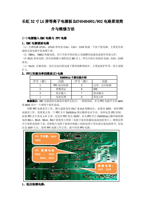
长虹32寸LG屏等离子电源板EAY40484901/902电路原理简介与维修方法(一)电源输入EMC电路与 PFC电路1、EMC电源滤波电路(1)互感线圈LF101、LF102和电容C101、C104、C105构成一个抗干扰电路,主要是用来滤除交流电源中的高频干扰。
(2)TH601、TH602热敏电阻,用于冷机开机时防止电源瞬间浪涌电流损坏其他元件。
(3)R101放电电阻,因为电源输入端阻抗达MΩ以上,所以关机后电阻给C101、C104、C105放电。
(4)VA101压敏电阻,电压过高内阻迅速下降而烧断保险丝,主要起保护作用,防止故障扩大。
2、PFC(有源功率因数校正)电路FAN5501A个脚功能介绍序号(脚)功能序号(脚)功能1 PFC高压检测 5 过零、过压检测2 参数设定 6 GND3 低压输入7 驱动输出4 电流反馈8 供电14V维修提示:EMC电源滤波电路损坏器件比较少,一般烧保险,多为PFC电路开关管Q602或Q603其中一个或两个损坏造成。
判断PFC电路是否工作,测大滤波电容C617或618两脚电压,如果有300V,说明PFC 电路没工作,需要重点查一下PFC芯片FAN5501A第⑧脚供电对不对,该供电受CPU控制,如果PFC芯片供电14V正常,还没有PFC电压(380V),多为PFC芯片FAN5501A①脚外接检测电阻R614、R615、R616、R617阻值变小所致(电阻下面有胶漏电造成电阻变小),维修过程中只需把电阻拆下来,再把贴片电阻下面和印制板上的胶处理干净从新安装电阻即可;如电压是380V左右,说明PFC电路工作正常,就不用查PFC电路。
PFC开关管:Q603Q602PFC检测电阻R614、R615R616、R617滤波电容:C617 C618(二)电压检测电路1、低压检测电路:220V交流电经D125、R144、 R142、 R123、 R137、 R138、 C126半波整流、滤波后变成直流电压,再经R139、 R140 、R141分压,给U121参考端提供一个大于2.5V电压,此时TL431阴极电位下降,PC151光耦导通,CPU IC701(17)脚有5V开机工作信号,CPU收到信号后25脚由低电位变成高电位控制5Vstb输出电压。
液晶显示屏背光灯及高压驱动电路原理与故障维修
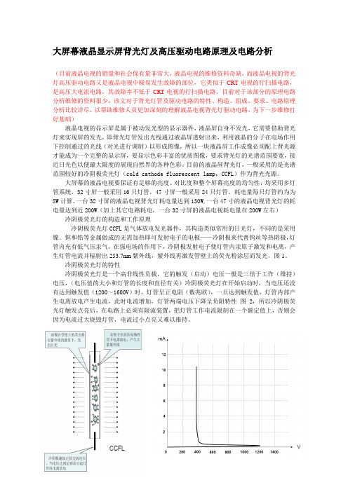
但是为了保证电容C和电感L的谐振频率就是振荡器的振荡频率,又要使电容C的容抗XC的大小基本正好是灯管的限流值,电路的精确设计是至关重要的。
在维修中,电容C是比较容易损坏的元件,如有损坏,一定要用和原来一样的电容代换,否则其性能会大幅下降,甚至不能使用。
对于多灯管屏的亮度控制,如果同时间断灯管的瞬间供电,PWM的间断频率会和液晶屏的刷新频率差拍,液晶屏会出现滚道干扰、闪烁、亮度不均匀等现象,为了防止这种现象产生,加于每个灯管的断续脉冲波相位上有所差异,即对灯管来说,短暂停止供电在多根灯管中,不是同时断电、供电,必须是交替轮流断电、供电。多灯管系统一般把灯管分为4组,供电系统的PWM脉冲有4个通道,输出4路经过PWM调制的高频脉冲波,每个通道向一组灯管供电,通道之间输出的PWM调制脉冲,依次移相900,这样4组灯管则达到轮流断电、供电,使亮度更均匀,干扰最小,三星32寸液晶屏有16根灯管,分为4组,每组4根灯管(24根灯管液晶屏的就每组6根灯管)。
所以目前冷阴极荧光灯的亮度控制均采用脉冲调光,具体方法是;用30~200Hz的低频PWM脉冲波(PWM脉冲波的宽度受控于CPU)对施加于冷阴极荧光灯管上的连续振荡高压进行调制,使连续振荡波变成断续振荡波,从而达到控制亮度的目的,其控制原理是;断续的在极短间内停止对冷阴极荧光灯供电,由于停止时间极短,不足以使灯管的电离状态消失,但是其辐射的紫外线强度下降,管壁上的荧光粉的激发量减小,亮度也下降,只要控制PWM的脉冲的占空比,就可以改变灯管在一个导通/关闭周期的时间比,从而达到控制灯管平均亮度的目的见图5中,调制器输出的脉冲串信号,目前的技术可以达到400:1或更高的调光控制。
FXXC PL3223三相三线 四线多功能数字电能表专用集成电路 说明书

FXXC®PL3223三相三线/四线多功能数字电能表专用集成电路性能特点:兼容三相三线以及三相四线高精度电能计量,符合IEC678/61036、GB/T 17215及IEC1268、GB/T 17882有功电能计量在1000:1的动态范围内误差小于0.1%无功电能计量在1000:1的动态范围内误差小于0.2%可精确测量至21次谐波的无功电能有功/无功校表脉冲输出瞬时有功/无功,线电压频率,电压/电流有效值测量同时提供分相及合相有功/无功及符号指示合相能量累加模式可选(代数相加/绝对值相加)两个步进电机驱动输出,可同时输出有功/无功功率断相/欠压/过压检测,具有中断输出电流通道内置可编程增益放大器(PGA)支持数字相位校正和小电流分段线性补偿内置数字式温度传感器,支持温度分段补偿电表常数、启动电流可数字调校SPI接口,方便外部微处理器控制各相实时电压电流AD波形数据;工业级温度标准,QFP44引脚封装功能描述:PL3223是一块高精度三相多功能电能计量芯片, 支持SPI接口和功率脉冲输出, 带有可自定义分频比的字轮驱动脉冲输出. PL3223整合了二阶Σ-ΔADC, 参考电压源, 温度传感器, 电源检测以及所有有功/无功电能计量和电压/电流有效值以及线电压频率测量的数字信号处理模块。
PL3223支持不同电网情况的有功和无功计量,如三相三线制,三相四线制;同时兼容各种电网频率,在50Hz标准和60Hz 标准频率的电网中均可实现高精度的功率计量。
除了通过脉冲输出管脚PCF和QCF提供有功功率和无功功率的实时信息之外,PL3223还提供电压和电流有效值以及线电压频率的计量功能(通过片内寄存器VRMS(34~37H)和IRMS(38~3BH)读取)。
用户可以根据电压电流的有效值计算得到视在功率。
PL3223内置有8个三相/合相有功无功功率脉冲的8位计数器,用以辅助外部MCU的脉冲计数,因此可以从根本上杜绝MCU 漏记脉冲的问题。
电位器封装
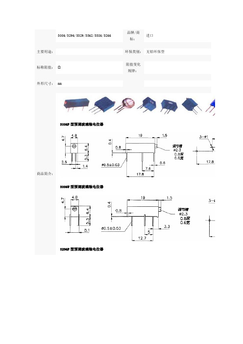
3006/3296/3329/3362/3386/3266品牌/商标:进口主要用途: 环保类别: 无铅环保型标称阻值: Ω 阻值变化规律:外形尺寸: mm商品简介:3006P 型预调玻璃釉电位器3006W 型预调玻璃釉电位器3296P 型预调玻璃釉电位器3296W型预调玻璃釉电位器3296X型预调玻璃釉电位器3296Y型预调玻璃釉电位器3296Z型预调玻璃釉电位器3329H型预调玻璃釉电位器3329P型预调玻璃釉电位器3329S型预调玻璃釉电位器3362P型预调玻璃釉电位器3362R型预调玻璃釉电位器3362U型预调玻璃釉电位器3362M型预调玻璃釉电位器3362W型预调玻璃釉电位器3386X型预调玻璃釉电位器3386W型预调玻璃釉电位器3386P型预调玻璃釉电位器3386U型预调玻璃釉电位器3266W型预调玻璃釉电位器3266X型预调玻璃釉电位器3266P型预调玻璃釉电位器3323P型预调玻璃釉电位器3323U型预调玻璃釉电位器3323W型预调玻璃釉电位器3323S型预调玻璃釉电位器3323V型预调玻璃釉电位器预调玻璃釉电位器产品技术参数项目3006 3296 3329 3362 3386 3266 阻值范围100Ω~1MΩ阻值偏差±10%终端电阻≤1%R或10Ω电阻规律 A转动噪声≤3%R或5Ω(取其较大者)温度系数±100ppm/°C机械耐久性200周旋转角度22±5圈28±2圈80°±10°260°±10°300°±10°12±2圈启动力矩3-35mN.m 3-35mN.m 3-30mN. 3-30mN.m 3-35mN.m3-30mN.m额定功耗0.75W 0.5W 0.5W 0.25W 0.5W 0.25W 耐电压640V AC 640V AC 510V AC 640V AC 600V AC 640V AC。
APD3224SYC
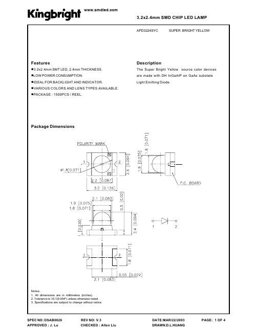
Description
The Super Bright Yellow source color devices are made with DH InGaAlP on GaAs substate Light Emitting Diode.
Package Dimensions
Notes: 1. All dimensions are in millimeters (inches). 2. Tolerance is ±0.1(0.004") unless otherwise noted. 3. Specifications are subject to change without notice.
CapacitБайду номын сангаасnce
Super Bright Yellow
Forward Voltage
Super Bright Yellow
Reverse Current
Super Bright Yellow
Typ. 590 588 28 25 2.0
Max.
2.5 10
Units nm nm nm pF V uA
Test Conditions I F =20mA I F =20mA I F =20mA
VF=0V;f=1MHz I F =20mA VR = 5V
Absolute Maximum Ratings at T)=25°C
Parameter
Power dissipation DC Forward Current Peak Forward Current [1] Reverse Voltage Operating/Storage Temperature
点击进入洸子其科技
士兰微电子 SD4931 电流模式 PWM 控制器 说明书

100V电流模式PWM控制器描述SD4931 是用于开关电源的内置100V高压MOSFET的电流模式PWM 控制器。
SD4931 内置高压启动电路。
在轻载下会进入打嗝模式,从而有效地降低系统的待机功耗。
具有降频功能,进一步优化轻载条件下的转换效率。
具有软启动功能,能够减小器件的应力,防止变压器饱和。
有VDD打嗝功能,不仅防止V DD欠压重启,也有效地降低待机功耗。
SD4931内部还集成了各种异常状态的保护功能,包括:VDD欠压保护,VDD过压保护,前沿消隐,输出短路保护,过流保护,过温保护等。
触发保护后,电路会不断自动重启,直到系统正常为止。
主要特点♦20V至100V输入电压♦12~15V输出电压♦1A输出电流♦高压启动♦轻载打嗝♦降频♦软启动♦VDD打嗝♦VDD欠压保护♦VDD过压保护♦前沿消隐♦输出短路保护♦过流保护♦过温保护应用♦平衡轮♦以太网供电♦电动自行车♦电动工具产品规格分类内部框图极限参数电气参数(除非特别说明, VDD =12V;Tamb=25︒C)管脚排列图管脚描述功能描述SD4931是用于开关电源的内置高压MOSFET的电流模式PWM控制器,内置高压启动电路,在轻载下会进入打嗝模式,具有降频、软启动、VDD打嗝,还集成了VDD欠压保护、VDD过压保护、前沿消隐、输出短路保护、过流保护、过温保护等各种异常状态的保护功能。
高压启动SD4931内置高压启动电路。
启动时,输入电压从DRAIN端通过内置高压启动恒流源,对VDD端外置电容进行充电,充电电流为1mA,使得VDD电压上升,当升至启动电压14.3V时,将高压启动恒流源关断,则DRAIN端对VDD 端停止充电,转由电感电压通过二极管对VDD端进行供电;如果VDD电压降至欠压保护点8.9V,则将高压启动恒流源重新打开,又由DRAIN端对VDD端进行充电,使得VDD电压上升,升至启动电压14.3V。
恒压控制SD4931通过FB脚检测VOUT的变化,当VOUT变小,流入FB脚的电流减小,从而增大输出脉宽,使VOUT上升,使输出保持恒定,VOUT电压近似等于ZD1两端电压。