HC26中文资料
LM26CIM5-HHD中文资料
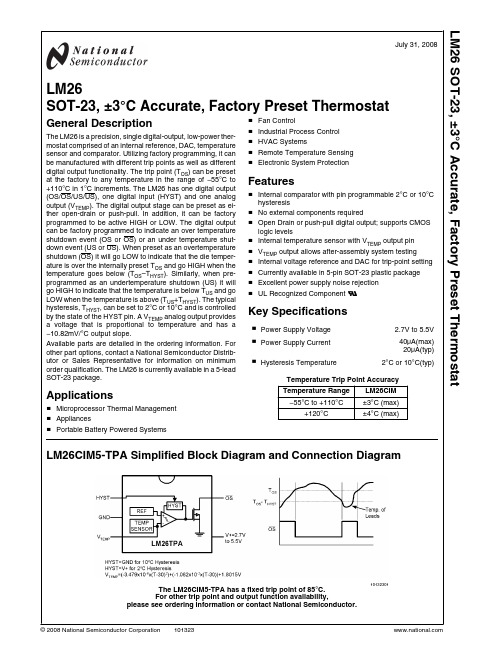
Analog output voltage proportional to temperature
Leave floating or connect to a high impedance node.
Supply input
2.7V to 5.5V with a 0.1µF bypass capacitor. For PSRR information see Section Titled NOISE CONSIDERATIONS.
Undertemperature Shutdown open-drain active System or power supply shutdown; pull-up resistor ≥ 10kΩ
low thermostat digital output
Undertemperature Shutdown push-pull active System or power supply shutdown high thermostat digital output
Overtemperature Shutdown open-drain active Controller interrupt, system or power supply shutdown; pull-up
low thermostat digital output
resistor ≥ 10kΩ
Overtemperature Shutdown push-pull active Controller interrupt, system or power supply shutdown high thermostat digital output
Available parts are detailed in the ordering information. For other part options, contact a National Semiconductor Distributor or Sales Representative for information on minimum order qualification. The LM26 is currently available in a 5-lead SOT-23 package.
HCNW2611中文资料

1-146HHigh CMR, High Speed TTL Compatible Optocouplers Technical Data6N137HCNW137HCNW2601HCNW2611HCPL-0600HCPL-0601HCPL-0611HCPL-0630CAUTION: It is advised that normal static precautions be taken in handling and assembly of this component to prevent damage and/or degradation which may be induced by ESD.Features• 5 kV/µs Minimum Common Mode Rejection (CMR) at V CM = 50 V for HCPL-X601/X631, HCNW2601 and10kV/µs Minimum CMR at V CM = 1000 V for HCPL-X611/X661, HCNW2611• High Speed: 10 MBd Typical • LSTTL/TTL Compatible • Low Input Current Capability: 5 mA• Guaranteed ac and dcPerformance over Temper-ature: -40°C to +85°C • Available in 8-Pin DIP,SOIC-8, Widebody Packages • Strobable Output (Single Channel Products Only)• Safety ApprovalUL Recognized - 2500 V rms for 1 minute and 5000V rms*for 1 minute per UL1577CSA ApprovedVDE 0884 Approved with V IORM = 630 V peak forHCPL-2611 Option 060 and V IORM =1414 V peak for HCNW137/26X1BSI Certified(HCNW137/26X1 Only)• MIL-STD-1772 Version Available (HCPL-56XX/66XX)Functional Diagram*5000 V rms/1 Minute rating is for HCNW137/26X1 and Option 020 (6N137, HCPL-2601/11/30/31, HCPL-4661) products only.HCPL-0631HCPL-0661HCPL-2601HCPL-2611HCPL-2630HCPL-2631HCPL-4661Applications• Isolated Line Receiver • Computer-Peripheral Interfaces• Microprocessor System Interfaces• Digital Isolation for A/D,D/A Conversion• Switching Power Supply • Instrument Input/Output Isolation• Ground Loop Elimination • Pulse Transformer Replacement• Power Transistor Isolation in Motor Drives• Isolation of High Speed Logic SystemsDescriptionThe 6N137, HCPL-26XX/06XX/4661, HCNW137/26X1 are optically coupled gates that combine a GaAsP light emitting diode and an integrated high gain photo detector. An enable input allows the detector to be strobed.The output of the detector IC isA 0.1 µF bypass capacitor must be connected between pins 5 and 8.CATHODEANODE GNDV V CC O ANODE 2CATHODE 2CATHODE 1ANODE 1GNDV V CC O2V E V O16N137, HCPL-2601/2611 HCPL-0600/0601/0611 HCPL-2630/2631/4661 NC NCLED ON OFF ON OFF ON OFFENABLEH H L L NC NCOUTPUTL H H H L HTRUTH TABLE (POSITIVE LOGIC)LED ON OFFOUTPUTL HTRUTH TABLE (POSITIVE LOGIC)5965-3594Ean open collector Schottky-clamped transistor. The internal shield provides a guaranteed common mode transient immunity specification of 5,000 V/µs for the HCPL-X601/X631 and HCNW2601, and 10,000 V/µs for the HCPL-X611/X661 and HCNW2611.This unique design providesmaximum ac and dc circuitisolation while achieving TTLcompatibility. The optocoupler acand dc operational parametersare guaranteed from -40°C to+85°C allowing troublefreesystem performance.The 6N137, HCPL-26XX, HCPL-06XX, HCPL-4661, HCNW137,and HCNW26X1 are suitable forhigh speed logic interfacing,input/output buffering, as linereceivers in environments thatconventional line receiverscannot tolerate and are recom-mended for use in extremely highground or induced noiseenvironments.Selection GuideNotes:1. Technical data are on separate HP publications.2. 15 kV/µs with V CM = 1 kV can be achieved using HP application circuit.3. Enable is available for single channel products only, except for HCPL-193X devices.1-1471-148Ordering InformationSpecify Part Number followed by Option Number (if desired).Example:HCPL-2611#XXX020 = 5000 V rms/1 minute UL Rating Option*060 = VDE 0884 V IORM = 630 Vpeak Option**300 = Gull Wing Surface Mount Option†500 = Tape and Reel Packaging OptionOption data sheets available. Contact Hewlett-Packard sales representative or authorized distributor for information.*For 6N137, HCPL-2601/11/30/31 and HCPL-4661 (8-pin DIP products) only.**For HCPL-2611 only. Combination of Option 020 and Option 060 is not available.†Gull wing surface mount option applies to through hole parts only.SchematicV FUSE OF A 0.1 µF BYPASS CAPACITOR CONNECTEDBETWEEN PINS 5 AND 8 IS RECOMMENDED (SEE NOTE 5).V CC V OGNDE6N137, HCPL-2601/2611 HCPL-0600/0601/0611V V CC V O1V V O2GNDHCPL-2630/2631/4661 HCPL-0630/0631/0661+ 0.076- 0.051(0.010+ 0.003)- 0.002)DIMENSIONS IN MILLIMETERS AND (INCHES).*MARKING CODE LETTER FOR OPTION NUMBERS"L" = OPTION 020"V" = OPTION 060OPTION NUMBERS 300 AND 500 NOT MARKED. Package Outline Drawings8-pin DIP Package** (6N137, HCPL-2601/11/30/31, HCPL-4661)8-pin DIP Package with Gull Wing Surface Mount Option 300(6N137, HCPL-2601/11/30/31, HCPL-4661)**JEDEC Registered Data (for 6N137 only).(0.025 ± 0.005)1.080 ± 0.320MAX.(0.100)BSCDIMENSIONS IN MILLIMETERS (INCHES).LEAD COPLANARITY = 0.10 mm (0.004 INCHES).+ 0.076- 0.051+ 0.003)- 0.002)1-1491-150Small-Outline SO-8 Package (HCPL-0600/01/11/30/31/61)8-Pin Widebody DIP Package (HCNW137, HCNW2601/11)(0.012)MIN.DIMENSIONS IN MILLIMETERS (INCHES).LEAD COPLANARITY = 0.10 mm (0.004 INCHES).1.78 ± 0.15 + 0.076 - 0.0051+ 0.003) - 0.002)1-1518-Pin Widebody DIP Package with Gull Wing Surface Mount Option 300(HCNW137, HCNW2601/11)Note: Use of nonchlorine activated fluxes is highly recommended.Solder Reflow Temperature Profile (HCPL-06XX and Gull Wing Surface Mount Option 300 Parts)240TIME – MINUTEST E M P E R A T U R E – °C2202001801601401201008060402002601.78 ± 0.15 MAX.BSCDIMENSIONS IN MILLIMETERS (INCHES).LEAD COPLANARITY = 0.10 mm (0.004 INCHES).Regulatory Information The 6N137, HCPL-26XX/06XX/ 46XX, and HCNW137/26XX have been approved by the following organizations:ULRecognized under UL 1577, Component Recognition Program, File E55361.CSAApproved under CSA ComponentAcceptance Notice #5, File CA88324.VDEApproved according to VDE0884/06.92. (HCPL-2611 Option060 and HCNW137/26X1 only)BSICertification according toBS415:1994(BS EN60065:1994),BS7002:1992(BS EN60950:1992) andEN41003:1993 for Class IIapplications. (HCNW137/26X1only)Insulation and Safety Related Specifications8-pin DIP Widebody(300 Mil)SO-8(400 Mil)Parameter Symbol Value Value Value Units Conditions Minimum External L(101)7.1 4.99.6mm Measured from input terminals Air Gap (External to output terminals, shortest Clearance)distance through air. Minimum External L(102)7.4 4.810.0mm Measured from input terminals Tracking (External to output terminals, shortest Creepage)distance path along body. Minimum Internal0.080.08 1.0mm Through insulation distance, Plastic Gap conductor to conductor, usually (Internal Clearance)the direct distance between thephotoemitter and photodetectorinside the optocoupler cavity. Minimum Internal NA NA 4.0mm Measured from input terminals Tracking (Internal to output terminals, along Creepage)internal cavity.Tracking Resistance CTI200200200Volts DIN IEC 112/VDE 0303 Part 1 (ComparativeTracking Index)Isolation Group IIIa IIIa IIIa Material Group(DIN VDE 0110, 1/89, Table 1) Option 300 - surface mount classification is Class A in accordance with CECC 00802.1-1521-153VDE 0884 Insulation Related Characteristics (HCPL-2611 Option 060 Only)*Refer to the front of the optocoupler section of the current catalog, under Product Safety Regulations section (VDE 0884), for a detailed description.Note: Isolation characteristics are guaranteed only within the safety maximum ratings which must be ensured by protective circuits in application.VDE 0884 Insulation Related Characteristics (HCNW137/2601/2611 Only)*Refer to the front of the optocoupler section of the current catalog, under Product Safety Regulations section (VDE 0884), for a detailed description.Note: Isolation characteristics are guaranteed only within the safety maximum ratings which must be ensured by protective circuits in application.Absolute Maximum Ratings* (No Derating Required up to 85°C)*JEDEC Registered Data (for 6N137 only).**Ratings apply to all devices except otherwise noted in the Package column.†0°C to 70°C on JEDEC Registration.Recommended Operating ConditionsParameter Symbol Min.Max.Units Input Current, Low Level I FL*0250µAInput Current, High Level[1]I FH**515mA Power Supply Voltage V CC 4.5 5.5VLow Level Enable Voltage†V EL00.8VHigh Level Enable Voltage†V EH 2.0V CC V Operating Temperature T A-4085°CFan Out (at R L = 1 kΩ)[1]N5TTL Loads Output Pull-up Resistor R L330 4 kΩ*The off condition can also be guaranteed by ensuring that V FL≤0.8 volts.**The initial switching threshold is 5 mA or less. It is recommended that 6.3 mA to 10 mA be used for best performance and to permit at least a 20% LED degradation guardband.†For single channel products only.1-154Electrical SpecificationsOver recommended temperature (T A = -40°C to +85°C) unless otherwise specified. All Typicals at V CC = 5 V, T A = 25°C. All enable test conditions apply to single channel products only. See note 5.*JEDEC registered data for the 6N137. The JEDEC Registration specifies 0°C to +70°C. HP specifies -40°C to +85°C.1-155Switching Specifications (AC)Over Recommended Temperature (T A = -40°C to +85°C), V CC = 5 V, I F= 7.5 mA unless otherwise specified. All Typicals at T A = 25°C, V CC = 5 V.*JEDEC registered data for the 6N137.**Ratings apply to all devices except otherwise noted in the Package column.1-156Package Characteristics= 25°C.All Typicals at T**The Input-Output Momentary Withstand Voltage is a dielectric voltage rating that should not be interpreted as an input-output continuous voltage rating. For the continuous voltage rating refer to the VDE 0884 Insulation Characteristics Table (if applicable), your equipment level safety specification or HP Application Note 1074 entitled “Optocoupler Input-Output Endurance Voltage.”†For 6N137, HCPL-2601/2611/2630/2631/4661 only.Notes:1. Each channel.2. Peaking circuits may produce transient input currents up to 50 mA, 50 ns maximum pulse width, provided average current doesnot exceed 20 mA.3. Peaking circuits may produce transient input currents up to 50 mA, 50 ns maximum pulse width, provided average current doesnot exceed 15 mA.4. Derate linearly above 80°C free-air temperature at a rate of 2.7 mW/°C for the SOIC-8 package.5. Bypassing of the power supply line is required, with a 0.1 µF ceramic disc capacitor adjacent to each optocoupler as illustrated inFigure 17. Total lead length between both ends of the capacitor and the isolator pins should not exceed 20 mm.6. The JEDEC registration for the 6N137 specifies a maximum I OH of 250 µA. HP guarantees a maximum I OH of 100 µA.7. The JEDEC registration for the 6N137 specifies a maximum I CCH of 15 mA. HP guarantees a maximum I CCH of 10 mA.8. The JEDEC registration for the 6N137 specifies a maximum I CCL of 18 mA. HP guarantees a maximum I CCL of 13 mA.9. The JEDEC registration for the 6N137 specifies a maximum I EL of –2.0 mA. HP guarantees a maximum I EL of -1.6 mA.10. The t PLH propagation delay is measured from the 3.75 mA point on the falling edge of the input pulse to the 1.5 V point on therising edge of the output pulse.11. The t PHL propagation delay is measured from the 3.75 mA point on the rising edge of the input pulse to the 1.5 V point on thefalling edge of the output pulse.12. t PSK is equal to the worst case difference in t PHL and/or t PLH that will be seen between units at any given temperature and specifiedtest conditions.13. See application section titled “Propagation Delay, Pulse-Width Distortion and Propagation Delay Skew” for more information.14. The t ELH enable propagation delay is measured from the 1.5 V point on the falling edge of the enable input pulse to the 1.5 Vpoint on the rising edge of the output pulse.15. The t EHL enable propagation delay is measured from the 1.5 V point on the rising edge of the enable input pulse to the 1.5 V pointon the falling edge of the output pulse.16. CM H is the maximum tolerable rate of rise of the common mode voltage to assure that the output will remain in a high logic state(i.e., V O > 2.0 V).17. CM L is the maximum tolerable rate of fall of the common mode voltage to assure that the output will remain in a low logic state(i.e., V O < 0.8 V).18. For sinusoidal voltages, (|dV CM | / dt)max = πf CM V CM(p-p).1-1571-158I O H – H I G H L E V E L O U T P U T C U R R E N T – µAT A – TEMPERATURE – °C1015519. No external pull up is required for a high logic state on the enable input. If the V E pin is not used, tying V E to V CC will result inimproved CMR performance. For single channel products only.20. Device considered a two-terminal device: pins 1, 2, 3, and 4 shorted together, and pins 5, 6, 7, and 8 shorted together.21. In accordance with UL1577, each optocoupler is proof tested by applying an insulation test voltage ≥ 3000 V rms for one second(leakage detection current limit, I I-O ≤ 5 µA). This test is performed before the 100% production test for partial discharge (Method b) shown in the VDE 0884 Insulation Characteristics Table, if applicable.22. In accordance with UL 1577, each optocoupler is proof tested by applying an insulation test voltage ≥ 6000 V rms for one second(leakage detection current limit, I I-O ≤ 5 µA). This test is performed before the 100% production test for partial discharge (Method b) shown in the VDE 0884 Insulation Characteristics Table, if applicable.23. Measured between the LED anode and cathode shorted together and pins 5 through 8 shorted together. For dual channel productsonly.24. Measured between pins 1 and 2 shorted together, and pins 3 and 4 shorted together. For dual channel products only.Figure 2. Typical Output Voltage vs. Forward Input Current.Figure 3. Typical Input Threshold Current vs. Temperature.Figure 1. Typical High Level Output Current vs. Temperature.1623I F – FORWARD INPUT CURRENT – mA 0V O – O U T P U T V O L T A G E – V8-PIN DIP, SO-81623I F – FORWARD INPUT CURRENT – mAV O – O U T P U T V O L T A G E – VWIDEBODY6360T A – TEMPERATURE – °C 20I T H – I N P U T T H R E S H O L D C U R R E N T – m A1458-PIN DIP, SO-86360T A – TEMPERATURE – °C20I T H – I N P U T T H R E S H O L D C U R R E N T – m A145WIDEBODY1-159706060T A – TEMPERATURE – °C5020I O L – L O W L E V E L O U T P U T C U R R E N T – m A400.80.460T A – TEMPERATURE – °C 0.20V O L – L O W L E V E L O U T P U T V O L T A G E – V0.10.50.7WIDEBODY0.30.6Figure 7. Typical Temperature Coefficient of Forward Voltage vs. Input Current.Figure 4. Typical Low Level Output Voltage vs. Temperature.Figure 5. Typical Low Level Output Current vs. Temperature.Figure 6. Typical Input Diode Forward Characteristic.0.80.4T A – TEMPERATURE – °C 0.20V O L – L O W L E V E L O U T P U T V O L T A G E – V0.10.50.78-PIN DIP, SO-80.30.6I F – F O R W A R D C U R R E N T – m A0.001V F – FORWARD VOLTAGE – V 1.010000.010.110100I F – F O R W A R D C U R R E N T – m A0.001V F – FORWARD VOLTAGE – V1.01100.010.110100d V F /d T – F O R W A R D V O L T A G E T E M P E R A T U R E C O E F F I C I E N T – m V /°C0.1110100I F – PULSE INPUT CURRENT – mA -1.4-2.2-2.0-1.8-1.6-1.2-2.48-PIN DIP, SO-8d V F /d T – F O R W A R D V O L T A G E T E M P E R A T U R E C O E F F I C I E N T – m V /°C0.1110100I F – PULSE INPUT CURRENT – mA-1.9-2.2-2.1-2.0-1.8-2.3WIDEBODY1-1604030T A – TEMPERATURE – °C 20P W D – P U L S E W I D T H D I S T O R T I O N – n s10-10Figure 8. Test Circuit for t PHL and t PLH .Figure 9. Typical Propagation Delay vs. Temperature.Figure 10. Typical Propagation Delay vs. Pulse Input Current.Figure 11. Typical Pulse Width Distortion vs. Temperature.Figure 12. Typical Rise and Fall Time vs. Temperature.10590I F – PULSE INPUT CURRENT – mA7530t P – P R O P A G A T I O N D E L A Y – n s6045OUTPUT V MONITORING NODEOOUTPUT V MONITORING NODEOI V FF*C L IS APPROXIMATELY 15 pF WHICH INCLUDES PROBE AND STRAY WIRING CAPACITANCE.10080T A – TEMPERATURE – °C600t P – P R O P A G A T I O N D E L A Y – n s4020t r , t f – R I S E , F A L L T I M E – n sT A – TEMPERATURE – °C1-161OUTPUT V MONITORING NODEOV V*C IS APPROXIMATELY 15 pF WHICH INCLUDES PROBE AND STRAY WIRING CAPACITANCE.LFigure 13. Test Circuit for t EHL and t ELH .Figure 14. Typical Enable Propagation Delay vs. Temperature.Figure 15. Test Circuit for Common Mode Transient Immunity and Typical Waveforms.V O0.5 VOV (MIN.)5 V0 V FSWITCH AT B: I = 7.5 mA FCM V HCM CM L OV (MAX.)CMV (PEAK)V Ot E– E N A B L E P R O P A G A T I O N D E L A Y – n sT A – TEMPERATURE – °C901203060+5 VOUTPUT V MONITORING NODE O PULSE GENERATOR Z = 50 ΩO+5 VOUTPUT V MONITORING NODEO PULSE GENERATOR Z = 50 ΩO1-162Figure 16. Thermal Derating Curve, Dependence of Safety Limiting Value with Case Temperature per VDE 0884.Figure 17. Recommended Printed Circuit Board Layout.O U T P U T P O W E R – P S , I N P U T C U R R E N T – I S0T S – CASE TEMPERATURE – °C400600800200100300500700ENABLE(SEE NOTE 5)OUTPUTDEVICE ILLUSTRATED.O U T P U T P O WE R – P S , I N P U T C U R R E N T – I S0T S – CASE TEMPERATURE – °C 4006008002001003005007001-163VDUAL CHANNEL DEVICE CC2*DIODE D1 (1N916 OR EQUIVALENT) IS NOT REQUIRED FOR UNITS WITH OPEN COLLECTOR OUTPUT.VCC2Figure 18. Recommended TTL/LSTTL to TTL/LSTTL Interface Circuit.Propagation Delay, Pulse-Width Distortion and Propagation Delay Skew Propagation delay is a figure of merit which describes how quickly a logic signal propagates through a system. The propaga-tion delay from low to high (t PLH) is the amount of time required for an input signal to propagate to the output, causing the output to change from low to high. Similarly, the propagation delay from high to low (t PHL) is the amount of time required for the input signal to propagate to the output causing the output to change from high to low (see Figure8).Pulse-width distortion (PWD) results when t PLH and t PHL differ in value. PWD is defined as the difference between t PLH and t PHL and often determines the maximum data rate capability of a transmission system. PWD can be expressed in percent by dividing the PWD (in ns) by the minimum pulse width (in ns) being transmitted. Typically, PWD on the order of 20-30% of the minimum pulse width is tolerable; the exact figure depends on the particular application (RS232,RS422, T-l, etc.).Propagation delay skew, t PSK, is an important parameter to consider in parallel data applica-tions where synchronization ofsignals on parallel data lines is aconcern. If the parallel data isbeing sent through a group ofoptocouplers, differences inpropagation delays will cause thedata to arrive at the outputs of theoptocouplers at different times. Ifthis difference in propagationdelays is large enough, it willdetermine the maximum rate atwhich parallel data can be sentthrough the optocouplers.Propagation delay skew is definedas the difference between theminimum and maximumpropagation delays, either t PLH ort PHL, for any given group ofoptocouplers which are operatingunder the same conditions (i.e.,the same drive current, supplyvoltage, output load, andoperating temperature). Asillustrated in Figure 19, if theinputs of a group of optocouplersare switched either ON or OFF atthe same time, t PSK is thedifference between the shortestpropagation delay, either t PLH ort PHL, and the longest propagationdelay, either t PLH or t PHL.As mentioned earlier, t PSK candetermine the maximum paralleldata transmission rate. Figure 20is the timing diagram of a typicalparallel data application with boththe clock and the data lines beingsent through optocouplers. Thefigure shows data and clocksignals at the inputs and outputsof the optocouplers. To obtain themaximum data transmission rate,both edges of the clock signal arebeing used to clock the data; ifonly one edge were used, theclock signal would need to betwice as fast.Propagation delay skew repre-sents the uncertainty of where anedge might be after being sentthrough an optocoupler. Figure20 shows that there will beuncertainty in both the data andthe clock lines. It is importantthat these two areas of uncertaintynot overlap, otherwise the clocksignal might arrive before all ofthe data outputs have settled, orsome of the data outputs maystart to change before the clocksignal has arrived. From theseconsiderations, the absoluteminimum pulse width that can besent through optocouplers in aparallel application is twice t PSK. Acautious design should use aslightly longer pulse width toensure that any additionaluncertainty in the rest of thecircuit does not cause a problem.The t PSK specified optocouplersoffer the advantages ofguaranteed specifications forpropagation delays, pulsewidthdistortion and propagation delayskew over the recommendedtemperature, input current, andpower supply ranges.1-1641-165Figure 19. Illustration of Propagation Delay Skew - t PSK .Figure 20. Parallel Data Transmission Example.I FV OI FVODATAINPUTSCLOCKDATAOUTPUTSCLOCK。
2,3-二氯丙烯特性表安全技术说明书
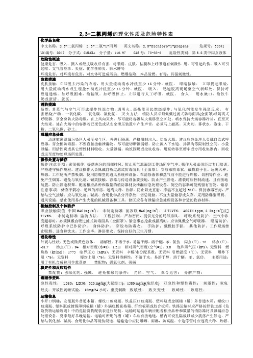
小开口钢桶;安瓿瓶外普通木箱;螺纹口玻璃瓶、铁盖压口玻璃瓶、塑料瓶或金属桶(罐)外普通木箱;螺纹口玻璃瓶、塑料瓶或镀锡薄钢板桶(罐)外满底板花格箱、纤维板箱或胶合板箱。铁路运输时应严格按照铁道部《危险货物运输规则》中的危险货物配装表进行配装。运输时运输车辆应配备相应品种和数量的消防器材及泄漏应急处理设备。夏季最好早晚运输。运输时所用的槽(罐)车应有接地链,槽内可设孔隔板以减少震荡产生静电。严禁与氧化剂、碱类、食用化学品等混装混运。运输途中应防曝晒、雨淋,防高温。中途停留时应远离火种、热源、高温区。装运该物品的车辆排气管必须配备阻火装置,禁止使用易产生火花的机械设备和工具装卸。公路运输时要按规定路线行驶,勿在居民区和人口稠密区停留。铁路运输时要禁止溜放。严禁用木船、水泥船散装运输。
操作处置与储存
操作注意事项:密闭操作,提供充分的局部排风。防止蒸气泄漏到工作场所空气中。操作人员必须经过专门培训,严格遵守操作规程。建议操作人员佩戴自吸过滤式防毒面具(全面罩),穿胶布防毒衣,戴橡胶手套。远离火种、热源,工作场所严禁吸烟。使用防爆型的通风系统和设备。在清除液体和蒸气前不能进行焊接、切割等作业。避免产生烟雾。避免与氧化剂、碱类接触。容器与传送设备要接地,防止产生静电。灌装时应控制流速,且有接地装置,防止静电积聚。配备相应品种和数量的消防器材及泄漏应急处理设备。倒空的容器可能残留有害物。储存注意事项:储存于阴凉、通风的库房。远离火种、热源。防止阳光直射。库温不宜超过30℃。保持容器密封,严禁与空气接触。应与氧化剂、碱类、食用化学品分开存放,切忌混储。不宜大量储存或久存。采用防爆型照明、通风设施。禁止使用易产生火花的机械设备和工具。储区应备有泄漏应急处理设备和合适的收容材料。
消防措施
易燃,其蒸气与空气可形成爆炸性混合物,遇明火、高热能引起燃烧爆炸。与氧化剂能发生强烈反应。有害燃烧产物:一氧化碳、二氧化碳、氯化氢。灭火方法:消防人员必须佩戴过滤式防毒面具(全面罩)或隔离式呼吸器、穿全身防火防毒服,在上风向灭火。尽可能将容器从火场移至空旷处。喷水保持火场容器冷却,直至灭火结束。处在火场中的容器若已变色或从安全泄压装置中产生声音,必须马上撤离。灭火剂:雾状水、泡沫、干粉、二氧化碳、砂土。
VC26H多功能过程校验仪说明书_中文(0.0)

多功能过程校验仪声明:本手册适用于HART型和基本型的多功能过程校验仪仪表。
与HART相关的操作仅适用于HART型。
手册内所有的解释和范例是以HART型型作说明的。
1引言多功能过程校验仪(以下简称校验仪)是一个由电池/适配器供电,能测量和输出电参数和物理参数的手持便携式仪器(见表1)。
表 1. 输出和测量功能一览表除表1所列的功能以外,校验仪还具有下列特性:▪任何功能状态都可直接进入HART功能(仅限HART型)。
▪测量和输出可同时工作。
测量信息与输出信息分屏显示。
▪热电偶(TC)输入/输出端子及校验仪内部具有自动参考节点温度补偿。
▪手动步进输出及自动步进和斜波电流输出。
▪任何操作下的室温监视▪测量/输出温度监视功能▪测量/输出mA%显示▪测量滤波功能▪测量手动保持功能▪压力输出显示值的自动保持功能2与我们联系欲订购部件、寻求操作上的协助或取得最靠近您的经销商或维修中心的地点,请打电话,或请探访公司网址:(见说明书封底)3标准配置以下所列的项目均包含在您的校验仪内,如果您发现校验仪有损坏或缺少一些东西,应立即与购买单位联系。
欲订购更换零件或备件,请参见本手册15.3所列的用户可更换的备件清单。
▪测试表笔(H000000-00) 1付▪工业测试导线(H000001-00) 1付▪工业测试导线(H000002-00) 1付▪钩式测试表笔(H000004-00) 1付▪鳄鱼夹(H010000-00) 1付▪鳄鱼夹(H010007-00) 1付▪热电偶转接头(H200000-00) 1个▪使用说明书 1本▪产品合格证明书 1份▪保险管(100mA/250V) 2只▪保险管(50mA/250V) 2只▪5号碱性电池 4节▪布包 1个4安全信息用户应按照本说明书的指示使用校验仪,否则校验仪所提供的保护措施可能会受到损坏。
对于没有按照所给的安全警示信息进行操”指出可能对用户构成危险的情况或行为;“小心”指出可能对校验仪或被测试设备造成损坏的情况或行为。
FLUKE 2620A 2625A 2635A中文手册
键,消除出错信
按
键,进入存储卡数据文件操作菜单,按
选择
“INIT”,即格式化,按
确认,面板显示“INIT NO”(不格
式化),按
键选择为“INIT YES”(格式化),按
确
存储卡的格式化流程图
―― 9 --
认,面板随后显示“SURE NO”(不确认),按
选择为“SURE YES”(确认进行格
式化),按
ALAR(监测报警发生后的数据)、TRANS(监测报警发生时的数
据),按
键确认。以后当按
键进行通道扫描时,
指定的测量扫描数据就会随这个设定记录到指定的位置。
扫描数据记录和打印流程图
4、监测报警的设置 Hydra 系列数据采集器具有 21 个模拟通道,每个通道都可以
设置两个独立的报警信号,每个报警信号又可以区分为“Lo”(低 限报警)、“Hi”(高限报警),并指定后面板的数字输出接口 DIO0~7 来连接相应的报警装置,如蜂鸣器、指示灯等。
按
键选择所要设置的通道,按
键进入报警设
置。按
键在“OFF”(没有报警)、“1”(第一报警点)、“2”(第
二报警点)选择一项,按
确认;再按
在“Lo”(低限报
警)、“Hi”(高限报警)中选择一项,按
确认;随后面板显
示“0.0000”,可按
和
将显示调整为具体报警点数值,
按
确认;随后系统要求确认小数点的位置,可根据设定值
存测量的数据、保存数据采集器的设置信息等。 (1) 存储卡的格式化
把存储卡后边的电池锁定 开关拨到另一边,拔出电池 夹,按所示极性方向装入电 池,按卡上箭头所示方向将 存储卡插入数据采集器插 槽,如果是新卡,面板上会
DS26LS32AC中文资料

DS26LS32AC中文资料TL F 5255DS26LS32C DS26LS32M DS26LS32AC DS26LS33C DS26LS33M DS26LS33AC Quad Differential Line ReceiversJanuary1996 DS26LS32C DS26LS32M DS26LS32ACDS26LS33CDS26LS33M DS26LS33AC Quad Differential Line Receivers General DescriptionThe DS26LS32and DS26LS32A are quad differential linereceivers designed to meet the RS-422 RS-423and Feder- al Standards1020and1030for balanced and unbalanceddigital data transmissionThe DS26LS32and DS26LS32A have an input sensitivity of 200mV over the input voltage range of g7V and theDS26LS33and DS26LS33A have an input sensitivity of500mV over the input voltage range of g15VBoth the DS26LS32A and DS26LS33A differ in functionfrom the popular DS26LS32and DS26LS33in that inputpull-up and pull-down resistors are included which prevent output oscillation on unused channelsEach version provides an enable and disable function com- mon to all four receivers and features TRI-STATE outputswith8mA sink capability Constructed using low powerSchottky processing these devices are available over thefull military and commerical operating temperature ranges FeaturesY High differential or common-mode input voltage ranges of g7V on the DS26LS32and DS26LS32A and g15Von the DS26LS33and DS26LS33AY g0 2V sensitivity over the input voltage range on theDS26LS32and DS26LS32A g0 5V sensitivity on theDS26LS33and DS26LS33AY DS26LS32and DS26LS32A meet all requirements ofRS-422and RS-423Y6k minimum input impedanceY100mV input hysteresis on the DS26LS32andDS26LS32A 200mV on the DS26LS33andDS26LS33AY Operation from a single5V supplyY TRI-STATE outputs with choice of complementary out-put enables for receiving directly onto a data bus Logic DiagramTL F 5255–1 Connection DiagramDual-In-Line PackageTL F 5255–2Top ViewTruth TableENABLE ENABLE Input Output01X Hi-ZSee V ID t V TH(Max)1Note Below VID s V TH(Min)0HI-Z e TRI-STATENote Input conditions may be any combination not defined for ENABLEand ENABLEOrder Number DS26LS32CM DS26LS32CNDS26LS32MJ DS26LS32ACM DS26LS32ACNDS26LS33CN DS26LS33MJ or DS26LS33ACNSee NS Package Number J16A M16A or N16AFor Complete Military883SpecificationsSee RETS Data SheetOrder Number DS26LS32MJ 883 DS26LS32MW 883DS26LS33MJ 883 DS26LS33MW 883See NS Package Number J16A or W16A TRI-STATE is aregistered trademark of National Semiconductor Corporation C1996National Semiconductor Corporation RRD-B30M36 Printed in U S A http www national comAbsolute Maximum Ratings(Note1)If Military Aerospace specified devices are required please contact the National Semiconductor Sales Office Distributors for availability and specifications Supply Voltage7V Common-Mode Range g25V Differential Input Voltage g25V Enable Voltage7V Output Sink Current50mA Maximum Power Dissipation at25 C Cavity Package1433mW Molded Dip Package1362mW SO Package DS26LS321002mWDS26LS32A1051mW Derate cavity package9 6mW C above25 C derate molded DIP package 10 9mW C above25 C Derate SO Package8 01mW C for DS26LS328 41mW C for DS26LS32A Storage T emperature Range b65C to a165 C Lead Temperature(Soldering 4seconds)260 C Operating ConditionsMin Max Units Supply Voltage (V CC)DS26LS32M DS26LS33M4 55 5V (MIL)DS26LS32C DS26LS33C4 755 25V DS26LS32AC DS26LS33AC (COML)Temperature (T A)DS26LS32M DS26LS33M b55a125 C (MIL)DS26LS32C DS26LS33C0a70 C DS26LS32AC DS26LS33AC(COML)Electrical Characteristics over the operating temperature range unless otherwise specified(Notes2 3and4) Symbol Parameter Conditions Min Typ Max UnitsV TH Differential Input V OUT e V OH DS26LS32 DS26LS32A b7V s V CM s a7V b0 2g0 070 2V Voltage or V OL DS26LS33DS26LS33A b15V s VCM a15V b0 5g0 140 5V R IN Input Resistance b15V s V CM s a15V(One Input AC GND)6 08 5k X I IN Input Current(Under V IN e15V Other Input b15V s V IN s a15V2 3mATest)VIN e b15V Other Input b15V s V IN s a15V b2 8mA V OH Output High Voltage V CC e MIN D V IN e1V Commercial2 74 2V V ENABLE e0 8V I OH e b440m A Military2 54 2V V OL Output Low Voltage V CC e Min D V IN e b1V I OL e4mA0 4V V ENABLE e0 8V IOL e8mA0 45V V IL Enable Low Voltage0 8V V IH Enable High Voltage2 0VV I Enable Clamp V CC e Min I IN e b18mAb1 5V VoltageI O OFF-State(High V CC e Max V O e2 4V20m AImpedance)OutputV O e0 4V b20m A CurrentI IL Enable Low Current V IN e0 4V b0 36mA I IH Enable High Current V IN e2 7V20m AI SC Output Short-Circuit V O e0V V CC e Max D V IN e1Vb15b85mA CurrentI CC Power Supply V CC e Max All V IN e GND DS26LS32 DS26LS32A5270mACurrent Outputs Disabled DS26LS33 DS26LS33A5780mA I I Input High Current V IN e5 5V100m A V HYST Input Hysteresis T A e25 C V CC e5V DS26LS32 DS26S32A100mVV CM e0V DS26LS33 DS26LS33A200mVNote1 ‘‘Absolute Maximum Ratings’’are those values beyond which the safety of the device cannot be guaranteed They are not meant to imply that the device should be operatedat these limits The table of‘‘Electrical Characteristics’’provides conditions for actual device operationNote2 All currents into device pins are shown as positive all currents out of device pins are shown as negative all voltages are referenced to ground unless otherwise specified All values shown as max or min are so classified on absolute value basis Note3 All typical values are V CC e5V T A e25 CNote4 Only one output at a time should be shortedhttp www national com2Switching Characteristics V CC e 5V T A e 25 CSymbol Parameter Conditions DS26LS32 DS26LS33DS26LS32A DS26LS33A UnitsMinTyp Max MinTyp Max t PLH Input to Output C L e 15pF 17252335ns t PHL 17252335ns t LZ ENABLE to Output C L e 5pF 20301530ns t HZ 15222025ns t ZL ENABLE to OutputC L e 15pF15221422ns t ZH15221522ns AC Test Circuit and Switching Time WaveformsLoad Test Circuit for TRI-STATE OutputsTL F 5255–3Propagation Delay (Notes 1and 3)TL F 5255–4Note 1 Diagram shown for ENABLE lowNote 2 S1and S2of load circuit are closed except whereshownNote 3 Pulse generator for all pulses Rate e 1 0MHz Z O e 50X t r s 6ns t f s 6 0nsEnable and Disable Times (Notes 2and 3)TL F 5255–5Typical ApplicationsTwo-Wire Balanced Interface RS-422TL F 5255–6Single Wire with Driver Ground Reference RS-423TL F 5255–7http www national com3Physical Dimensions inches(millimeters)Order Number DS26LS32MJ DS26LS33MJ DS26LS32MJ 883or DS26LS33MJ 883NS Package Number J16ASmall Outline Package(M)Order Number DS26LS32CM or DS26LS32ACMNS Package Number M16Ahttp www national com4Physical Dimensions inches(millimeters)(Continued)Order Number DS26LS32CN DS26LS32ACN DS26LS33CN or DS26LS33ACNNS Package Number N16A5http www national comD S 26L S 32C D S 26L S 32M D S 26L S 32A C D S 26L S 33C D S 26L S 33M D S 26L S 33A C Q u a d D i f f e r e n t i a l L i n e R e c e i v e r sPhysical Dimensions inches (millimeters)(Continued)16Lead Ceramic Flatpak (W)Order Number DS26LS32MW 883or DS26LS33MW 883NS Package Number W16ALIFE SUPPORT POLICYNATIONAL’S PRODUCTS ARE NOT AUTHORIZED FOR USE AS CRITICAL COMPONENTS IN LIFE SUPPORT DEVICES OR SYSTEMS WITHOUT THE EXPRESS WRITTEN APPROVAL OF THE PRESIDENT OF NATIONAL SEMICONDUCTOR CORPORATION Asused herein 1 Life support devices or systems are devices or 2 A critical component is any component of a life systems which (a)are intended for surgical implant support device or system whose failure to perform can into the body or (b)support or sustain life and whose be reasonably expected to cause the failure of the life failure to perform when properly used in accordance support device or system or to affect its safety or with instructions for use provided in the labeling can effectivenessbe reasonably expected to result in a significant injury to the userNational Semiconductor National Semiconductor National Semiconductor National Semiconductor Corporation EuropeHong Kong LtdJapan Ltd1111West Bardin RoadFax a 49(0)180-530858613th Floor Straight Block Tel 81-043-299-2308。
HD26LS32FP资料
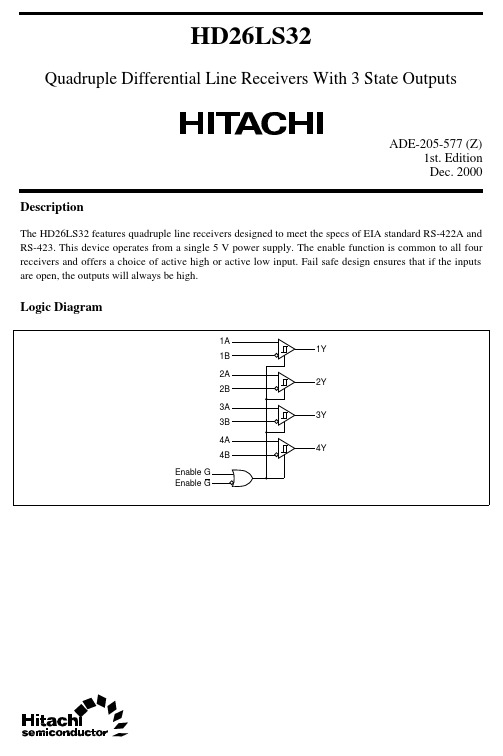
HD26LS32Quadruple Differential Line Receivers With 3 State OutputsADE-205-577 (Z)1st. EditionDec. 2000 DescriptionThe HD26LS32 features quadruple line receivers designed to meet the specs of EIA standard RS-422A and RS-423. This device operates from a single 5 V power supply. The enable function is common to all four receivers and offers a choice of active high or active low input. Fail safe design ensures that if the inputs are open, the outputs will always be high.Logic DiagramHD26LS322Pin ArrangementFunction TableDifferential Input Enable Output A – B G G Y V ID ≥ V THH X H X L H V TL < V ID < V TH H X ?X L ?V ID ≤ V TL H X L X L L X LHZH :High level L :Low level X :Immaterial ?:IrrelevantZ:High impedanceHD26LS323Absolute Maximum RatingsItemSymbol Ratings Unit Supply Voltage V CC *17.0V In Phase Input Voltage V IC ±25V Differential Input Voltage V ID *2±25V Enable Input Voltage V IN 7V Output Sink Current Iout 50mA Continuous Total Dissipation P T 1W Operating Temperature Range Topr 0 to +70°C Storage Temperature RangeTstg–65 to 150°CNotes: 1.All voltage values except for differential input voltage are with respect to network groundterminal.2.Differential input voltage is measured at the noninverting input with respect to the correspondinginverting onput.3.The absolute maximum ratings are values which must not individually be exceeded, andfurthermore, no two of which may be realized at the same time.Recommended Operating ConditionsItemSymbol Min Typ Max Unit Supply Voltage V CC 4.75 5.00 5.25V In Phase Input Voltage V IC ——±7.0V Output Current I OH ——–440µA I OL ——8mA Operating TemperatureTopr—70°CHD26LS324Electrical Characteristics (Ta = 0 to +70°C)ItemSymbol Min Typ*1Max Unit Conditions Differential Input High Threshold Voltage V TH ——0.2VV IC = –7 to +7 V V OH = 2.7 V, I OH = –440 µADifferential Input Low V TL——–0.2V OL = 0.4 V, I OL = 4 mA Threshold Voltage ——–0.2V OL = 0.45 V, I OL = 8 mAInput Hysteresis*2V TH – V TL —30—mV Enable Input Voltage V IH 2.0——VV IL ——0.8Enable Input Clamp Voltage V IK —— 1.5V CC = 4.75 V, I IN = –18 mA Output VoltageV OH 2.7——V CC = 4.75 V V ID = 1 V, I OH = –440 µA V OL——0.4V IL (G ) = 0.8 VV ID = –1 V, I OL = 4 mA ——0.45V ID = –1 V, I OL = 8 mA Off State (High I OZ——20µAV CC = 5.25 VV O = 2.4 V Impedance) Output Current——–20V O = 0.4 VLine Input Current I I———— 2.32.8mA V I = 15 V, Other Inputs –10 to +15 V V I = –15 V, Other Inputs –15 to +10 V Enable Input CurrentI I (EN)——100µA V I = 5.5 V I IH ——20V I = 2.7 V I IL——–0.36mA V I = 0.4 VInput Resistance ri 69.8—k ΩV IC = –15 to +15 V (Other Inputs AC GND)Short Circuit Output Current I OS *3–15—–85mA V CC = 5.25 VSupply CurrentI CC —5270V CC = 5.25 V, V I = 0 V (All Outputs Disable)Notes: 1.All typical values are at V CC = 5 V, Ta = 25°C,VIC = 0.2.Hysteresis is the differential between the positive going input threshold voltage and the negativegoing input threshold voltage.3.Not more than one output should be shorted at a time.Switching Characteristics (V CC = 5 V, Ta = 25°C)TItemSymbol Min typ Max Unit Conditions Propagation Delay Time t PLH , t PHL —1725nsC L = 15 pFOutput Enable Time t ZH , t ZL —1522Output Disable Timet HZ —1522C L = 5 pFt LZ—2030HD26LS3251. t PLH , t PHL Test circuitWaveformsHD26LS3262. t HZ , t ZH Test circuitWaveformsHD26LS3273. t LZ , t ZL Test circuitWaveformsHD26LS328HD26LS32 Line Receiver ApplicationsThe HD26LS32 is a line receiver that meets the EIA RS-422A and RS-423A conditions. It has a high in-phase input voltage range, both positive and negative, enabling highly reliable transmission to be performed even in noisy environments.Its main features are listed below.• Operates on a single 5 V power supply.• Three-state output• On-chip fail-safe circuit• ±7 V in-phase input voltage range • ±200 mV input sensitivity •Minimum 6 k input resistanceA block diagram is shown in figure 1. The enable function is common to all four drivers, and either active-high or active-low input can be selected.When exchange is carried out using a party line system, it is better to keep the receiver input bias current constituting the driver load small, as this allows more receivers to be connected.Consequently, whereas an input resistance of 4 k or above is stipulated in RS-422A and RS-423A, the HD26LS32 has been designed to allow a greater margin, with a minimum resistance of 6 k .Figure 2 shows the input current characteristics of the HD26LS32.The shaded areas in the graph indicate the input current allowable range stipulated in RS-422A and RS-423A.HD26LS32 output is LS-TTL compatible and has a three-state function, enabling the output to be placed in the high-impedance state, and so making the device suitable for bus line type applications.With an in-phase input voltage range of ±7 V and a ±200 mV input sensitivity, the HD26LS32 can withstand use in noisy environments.Also, since signals sent over a long-distance transmission line require a long transition time, it also takes a long time to cross the receiver’s input threshold level.Therefore, the input is provided with hysteresis of around 30 mV to prevent receiver output misoperation due to noise.An example of input hysteresis is shown in figure 3.The fail-safe function consists of resistances R connecting input A to V CC and input B to GND, as shown in figure 4.HD26LS329This circuit provides for the receiver input section to be pulled up or down by a high resistance that prevents it from becoming a driver load so that the output goes high in the event of a transmission line breakage or connector detachment.When the input pin is placed in the open state by the pull-up/pull-down resistance, the differential input voltage V ID is as follows:V ID : (V IA – V IB ) ≥ 0.2 Vand the output is fixed high.However, if the receiver-side termination resistance remains connected despite a line breakage or connector detachment, the output will be undetermined (figure 5).Figure 1 HD26LS32 Block DiagramFigure 2 Input Voltage vs. Input Current CharacteristicsHD26LS3210Figure 3 Differential Input Voltage vs. Output Voltage CharacteristicsFigure 4 Fail-Safe FunctionThis is because, since the termination resistance is normally matched to the transmission line characteristic impedance, the value falls to several tens of hundreds of ohms, and the differential input pins are shorted by this termination resistance. That is, the differential input voltage V ID comes within the rangeV ID : –0.2 V < V IA – V IB < 0.2 Vand the output becomes undetermined.To prevent this, resistance R 1 is inserted in series with the transmission line as shown in figure 6,minimizing the effect of the termination resistance. Resistance R 2 is added to increase the current flowing between the termination resistance and R 1, enabling the value of R 1 to be kept small.Inserting resistances R 1 and R 2 in this way provides for the differential input voltage V ID to become 200 mV or higher, but the following points must be noted.• Smallest possible R 1 valueIf this value is large, the receiver input sensitivity will fall.• Largest possible R 2 valueIf this value is small, the load on the driver will be large.Figure 7 shows experimental differential input voltages for variations in R 1 and R 2.Figure 5 Examples of Transmission Line DisconnectionFigure 6 Method of Enhancing Fail-Safe FunctionFigure 7 R1, R2vs. Differential Input VoltageRS-442A Interface Standard ApplicationsFigure 9 shows sample operation waveforms at various points with 1200 m and 12 m cable lengths.1.Unidirectional Transmission (1 : 1 Configuration)Figure 8 1 : 1 Unidirectional TransmissionFigure 9 Sample Transmission Waveforms2.Unidirectional Transmission (1 : n Configuration)Figure 10 1 : n Unidirectional TransmissionWith this connection method, n receivers are connected for one driver. In the RS-422A standard, ten receivers can be connected simultaneously for one driver.Conversely, it is also possible to connect one receiver for n drivers.Bidirectional Transmission3.When bidirectional data exchange is performed using a combination of the HD26LS31 and HD26LS32, since either high or low output control is possible, using complementary enable inputs for the driver and receiver makes it easy to configure the kind of combination illustrated in figure 11 .Extending this combination makes it possible to exchange n-bit data simultaneously, and handle a party line system.Package DimensionsCautions1.Hitachi neither warrants nor grants licenses of any rights of Hitachi’s or any third party’s patent,copyright, trademark, or other intellectual property rights for information contained in this document.Hitachi bears no responsibility for problems that may arise with third party’s rights, includingintellectual property rights, in connection with use of the information contained in this document.2.Products and product specifications may be subject to change without notice. Confirm that you have received the latest product standards or specifications before final design, purchase or use.3.Hitachi makes every attempt to ensure that its products are of high quality and reliability. However,contact Hitachi’s sales office before using the product in an application that demands especially high quality and reliability or where its failure or malfunction may directly threaten human life or cause risk of bodily injury, such as aerospace, aeronautics, nuclear power, combustion control, transportation,traffic, safety equipment or medical equipment for life support.4.Design your application so that the product is used within the ranges guaranteed by Hitachi particularly for maximum rating, operating supply voltage range, heat radiation characteristics, installationconditions and other characteristics. Hitachi bears no responsibility for failure or damage when used beyond the guaranteed ranges. Even within the guaranteed ranges, consider normally foreseeable failure rates or failure modes in semiconductor devices and employ systemic measures such as fail-safes, so that the equipment incorporating Hitachi product does not cause bodily injury, fire or other consequential damage due to operation of the Hitachi product.5.This product is not designed to be radiation resistant.6.No one is permitted to reproduce or duplicate, in any form, the whole or part of this document without written approval from Hitachi.7.Contact Hitachi’s sales office for any questions regarding this document or Hitachi semiconductor products.Hitachi, Ltd.Semiconductor & Integrated Circuits.Nippon Bldg., 2-6-2, Ohte-machi, Chiyoda-ku, Tokyo 100-0004, Japan Tel: Tokyo (03) 3270-2111 Fax: (03) 3270-5109Copyright © Hitachi, Ltd., 2000. All rights reserved. Printed in Japan.Hitachi Asia Ltd. Hitachi Tower16 Collyer Quay #20-00, Singapore 049318Tel : <65>-538-6533/538-8577 Fax : <65>-538-6933/538-3877URL : .sg URLNorthAmerica : /Europe : /hel/ecg Asia : Japan : http://www.hitachi.co.jp/Sicd/indx.htmHitachi Asia Ltd.(Taipei Branch Office)4/F, No. 167, Tun Hwa North Road, Hung-Kuo Building, Taipei (105), Taiwan Tel : <886>-(2)-2718-3666 Fax : <886>-(2)-2718-8180 Telex : 23222 HAS-TPURL : Hitachi Asia (Hong Kong) Ltd. Group III (Electronic Components) 7/F., North Tower, World Finance Centre,Harbour City, Canton Road Tsim Sha Tsui, Kowloon, Hong KongTel : <852>-(2)-735-9218 Fax : <852>-(2)-730-0281URL : Hitachi Europe Ltd.Electronic Components Group.Whitebrook ParkLower Cookham Road MaidenheadBerkshire SL6 8YA, United Kingdom Tel: <44> (1628) 585000Fax: <44> (1628) 585160Hitachi Europe GmbHElectronic Components Group Dornacher Stra βe 3D-85622 Feldkirchen, Munich GermanyTel: <49> (89) 9 9180-0Fax: <49> (89) 9 29 30 00Hitachi Semiconductor (America) Inc.179 East Tasman Drive,San Jose,CA 95134 Tel: <1> (408) 433-1990Fax: <1>(408) 433-0223For further information write to:Colophon 2.0。
MSDS物质安全资料表
MSDS大全目录表1-001 乙炔气 (1)表1-002 氧气 (2)表1-003 二氧化碳 (3)表1-004 氢气 (4)表1-005 氩气 (5)表1-006 甲烷 (6)表1-007 四氢噻吩 (7)表1-008 活性炭 (8)Active carbon (8)表1-009 三乙胺 (9)表1-010 硫代磷酰氯 (10)表1-011 硫黄 (11)表1-012 甲胺磷 (12)表1-013 多聚甲醛 (13)表1-014(附表1-3)甲缩醛 (14)表1-015 黄磷 (15)表1-016 氯 (16)表1-017 三氯化磷 (17)表1-018 甲醇 (19)表1-019 液碱 (20)表1-020 氨水 (21)表1-021 硫酸二甲酯 (22)表1-022 甲胺磷 (23)表1-023 液氨 (24)表1-024 氯仿 (25)表1-025 二氯乙烷 (26)表1-026 二硫化碳 (27)表1-027 甲苯 (28)表1-028 盐酸 (29)表1-029 氯甲烷 (30)表1-030 硫酸 (31)表1-031 二甲苯 (33)表1-032 醋酸酐 (34)表1-033 多聚甲醛 (35)表1-034 草甘膦 (36)表1-035 稻瘟灵 (37)表1-036 异丙胺 (38)表1-037 漂白粉 (39)表1-038 氯化氢 (40)表1-039 氰化氢 (41)表1-040 氰化钠 (42)表1-042 甲缩醛 (44)表1-043 丙烯腈 (45)表1-044 氧化亚铜 (46)表1-045 四氯化锡 (47)表1-046 四氧化三铅 (48)表1-047 三氯化铝(无水) (49)表1-048 松香水 (50)表1-049红丹油性防锈漆 (51)表1-050 酚醛树脂 (52)表1-051 硫磺粉(补充) (53)表1-052 一乙胺 (54)表1-053三聚氯氰 (55)表1-054 三氯乙烯 (57)表1-055 磷酸 (58)表1-056 四丁基锡 (59)表1-057 柴油 (60)表1-058 对氨基苯酚 (61)表1-059 醋酸乙酯 (62)表1-060 对氯硝基苯 (63)表1-061 氮气 (64)表1-062莠去津 (65)表1-063 扑草净 (66)表1-064 八氯二丙醚 (67)表1-065 硫化钠 (68)表1-066 异丙醇 (69)表1-067 丙酮 (70)表1-068 二氯丙烷 (71)表1-069 环己酮 (72)表1-070 乙酸异戊酯 (73)表1-071 锌粉 (74)表1-072 乙醇 (75)表1-073 次氯酸钠溶液 (76)表1-074 石脑油 (77)表1-075 双环戊二烯 (78)表1-076 乙酸丁酯 (79)表1-077 双氧水 (80)表1-078 丙烯酸丁酯 (81)表1-079 丙烯酸 (82)表1-080 苯乙烯 (83)表1-081 过硫酸铵 (84)表1-082 过硫酸钾 (85)表1-083 丙烯酰胺 (86)表1-084 甲醛 (87)表1-086 甲基丙烯酸 (89)表1-087 汽油 (90)表1-088 乙酸 (91)表1-089 丙烯酸树脂 (92)表1-090 丙烯酸清漆 (93)表1-091 丙烯酸漆稀释剂 (94)表1-092 丙烯酸磁漆 (95)表1-093 二乙醇胺 (97)表1-094 煤油 (98)表1-095 漂白粉 (99)表1-096 漂粉精 (100)表1-097 三氯异氰尿酸 (101)表1-098 松香 (102)表1-099 松节油 (103)表1-100 硫化钠 (104)表1-101 保险粉 (105)表1-102 7385聚氨酯清漆(分装) (106)表1-103 甲酸 (107)表1-104 乙酸乙二醇乙醚 (108)表1-105 H-3聚氨酯漆固化剂 (109)表1-106 聚氨酯漆稀释剂 (110)表1-107 263醇酸树脂 (111)表1-108 异噻唑啉酮 (112)表1-109 N-乙基苯胺 (113)表1-110苯胺 (114)表1-111 乙酰甲胺磷 (115)表1-112 亚磷酸 (117)表1-113 亚磷酸二甲酯 (118)表1-114 氯甲烷 (119)表1-115 乙醚 (120)表1-116 丙烯酸甲酯 (121)表1-117 一甲胺 (122)表1-118 硝酸镁 (123)表1-119 硫化氢 (124)表1-120 硫化铵 (125)表1-121 一甲胺水溶液 (126)表1-122 兔宝宝面漆 (127)表1-123 兔宝宝稀释剂 (128)表1-124 硫氢化钠 (129)表1-125丙酸 (130)表1-126乙酰氯 (131)表1-127丙酰氯 (132)表1-128 丁醇 (133)表1-129 醇酸调合漆(未列名) (134)表1-129 碳化钙、电石 (135)表1-130 硝酸钠 (136)表1-131 溴甲烷 (137)表1-132 磷化铝 (138)表1-133 正丁醇 (139)表1-134 硝基木器漆 (140)表1-135 硝化棉(含氮≤12.6%) (141)表1-136 单丁醚 (142)表1-137 砷 (143)表1-138 碘化汞 (144)表1-139 氯化汞 (145)表1-140 叠氮化钠 (146)表1-141 重铬酸钠 (147)表1-142 高锰酸钾 (148)表1-143 氰化金钾 (149)表1-144丙烯酸 (150)表1-145甲基丙烯酸甲酯 (151)表1-146苯乙烯 (152)表1-147丙烯酸丁酯 (153)表1-148丁醇 (154)表1-149偶氮二异丁腈 (155)表1-150甲基丙烯酸异丁酯 (156)表1-151 甲基丙烯酸(正)丁酯 (157)表1-152 乙酰丙酮 (158)表1-153 2-丁酮 (160)表1-154 生松香 (161)表1-155 硫酸铜 (162)表1-155 硝酸 (163)表1-155 氰化钾 (164)表1-156硝基苯 (165)表1-157 氟化钠 (166)表1-158 氢氟酸 (167)表1-159蓄电池(注有酸液) (168)表1-160 环氧树脂 (169)表1-161 氯苯 (170)表1-162 乙苯 (171)表1-163 樟脑 (172)表1-164 赛璐珞 (173)表1-165 氢氧化钾 (174)表1-166 乙酸丁酯 (175)表1.6.7 NN-二甲基甲酰胺 (176)表1.6.8 叔丁胺 (177)表1.6.9氯化亚砜 (178)表1-001 乙炔气表1-002 氧气表1-003 二氧化碳表1-004 氢气表1-005 氩气表1-006 甲烷表1-007 四氢噻吩表1-008 活性炭活性炭 C 12.0Active carbon别名:Activated chlarcoal危规分类及编号:自燃物品。
化学品的安全防护规则的技术说明书新

化学品的安全防护规则的技术说明书新化学品安全技术说明书
化学品的安全防护规则的技术说明书新二〇〇六年二月
目录
表1-008 活性炭
Active carbon
又名:Activated chlarcoal
危规分类及编号:自燃物件。
GB4.2类42521。
UN NO.1362。
IMDG CODE 4224页,4.2类。
(国内作一般货物运输)
规格工业级粉状活性炭(LY216-79)分:781型、782型、783型
用途颗粒活性炭用于有机溶剂蒸气的回收,有机合成催化剂或载体,去除空气中的不纯物,糖、酒精、食品等溶液的精制,粉末活性炭用于去除沙糖、饴糖等的色素,乙醇饮料的调味、脱色、脱臭及油脂和医药等的脱臭、脱色,并用作药用炭等。
物化性质33以上。
化学性质稳固,熔点3500℃以上,沸点4000℃。
不溶于水和任何溶剂。
危险特征粉尘接触明火有轻度的爆炸性。
在空气中易迟缓地发热和自燃。
属基本无毒地物质。
但有时从原猜中夹杂无机物,对皮肤、黏膜及呼吸道有必定的刺激。
储运须知包装方法(Ⅲ)类。
牛皮纸外塑料袋,气密封口。
储运条件:储藏于干燥、通风的库房,远离火种、热源,不行与氧化剂共储混运,防备受潮,以防止受潮后积热不散可能发生自燃。
如抽查发现有发热现象应实时倒垛散热,防备发惹祸故。
泄露办理:扫起,倒至垃圾箱内。
(液氨见表1-23)
(氨水见表1-20)。
BYV26C-TR;中文规格书,Datasheet资料
Ultra Fast Avalanche Sinterglass DiodeBYV26A, BYV26B, BYV26C, BYV26D, BYV26EVishay SemiconductorsDocument Number: 86040For technical questions within your region, please contact one of the following:MECHANICAL DATACase: SOD-57Terminals: plated axial leads, solderable per MIL-STD-750,method 2026Polarity: color band denotes cathode end Mounting position: any Weight: approx. 369 mgFEATURES•Glass passivated junction •Hermetically sealed package •Very low switching losses •Low reverse current •High reverse voltage•Compliant to RoHS directive 2002/95/EC and in accordance to WEEE 2002/96/EC•Halogen-free according to IEC 61249-2-21 definitionAPPLICATIONS•Switched mode power supplies •High-frequency inverter circuits949539PARTS TABLEPART TYPE DIFFERENTIATION PACKAGE BYV26A V R = 200 V; I FAV = 1 A SOD-57BYV26B V R = 400 V; I FAV = 1 A SOD-57BYV26C V R = 600 V; I FAV = 1 A SOD-57BYV26D V R = 800 V; I FAV = 1 A SOD-57BYV26EV R = 1000 V; I FAV = 1 ASOD-57ABSOLUTE MAXIMUM RATINGS (T amb = 25°C, unless otherwise specified)PARAMETERTEST CONDITIONPART SYMBOL VALUE UNIT Reverse voltage = repetitive peak reverse voltageSee electrical characteristicsBYV26AV R = V RRM 200V BYV26BV R = V RRM 400V BYV26C V R = V RRM 600V BYV26D V R = V RRM 800V BYV26EV R = V RRM1000V Peak forward surge current t p = 10 ms, half sine waveI FSM 30A Average forward currentI FAV 1A Non repetitive reverse avalanche energyI (BR)R = 1 A, inductive load E R 10mJ Junction and storage temperature rangeT j = T stg- 55 to + 175°CMAXIMUM THERMAL RESISTANCE (T amb = 25°C, unless otherwise specified)PARAMETER TEST CONDITION SYMBOL VALUE UNIT Junction ambientl = 10 mm, T L = constantR thJA45K/WBYV26A, BYV26B, BYV26C, BYV26D, BYV26EVishay SemiconductorsUltra Fast Avalanche SinterglassDiode For technical questions within your region, please contact one of the following:Document Number: 86040TYPICAL CHARACTERISTICS (T amb = 25 °C, unless otherwise specified)Fig. 1 - Max. Reverse Power Dissipation vs. Junction Temperature Fig. 2 - Max. Reverse Current vs. Junction Temperature Fig. 3 - Max. Average Forward Current vs. Ambient TemperatureFig. 4 - Max. Reverse Current vs. Junction TemperatureELECTRICAL CHARACTERISTICS (T amb = 25°C, unless otherwise specified)PARAMETER TEST CONDITIONPARTSYMBOLMIN.TYP.MAX.UNIT Forward voltage I F = 1 A V F -- 2.5V I F = 1 A, T j = 175 °CV F -- 1.3V Reverse currentV R = V RRMI R --5μA V R = V RRM , T j = 150°CI R --100μA Reverse breakdown voltageI R = 100 μABYV26A V (BR)R 300--V BYV26BV (BR)R 500--V BYV26C V (BR)R 700--V BYV26D V (BR)R 900--V BYV26E V (BR)R 1100--V Reverse recovery timeI F = 0.5 A, I R = 1 A, i R = 0.25 ABYV26A t rr --30ns BYV26Bt rr --30ns BYV26C t rr --30ns BYV26D t rr --75ns BYV26E t rr--75nsBYV26A, BYV26B, BYV26C, BYV26D, BYV26EUltra Fast Avalanche SinterglassDiodeVishay SemiconductorsDocument Number: 86040For technical questions within your region, please contact one of the following:Fig. 5 - Diode Capacitance vs. Reverse Voltage Fig. 6 - Diode Capacitance vs. Reverse VoltagePACKAGE DIMENSIONS in millimeters (inches): SOD-57Legal Disclaimer Notice VishayDisclaimerALL PRODU CT, PRODU CT SPECIFICATIONS AND DATA ARE SU BJECT TO CHANGE WITHOU T NOTICE TO IMPROVE RELIABILITY, FUNCTION OR DESIGN OR OTHERWISE.Vishay Intertechnology, Inc., its affiliates, agents, and employees, and all persons acting on its or their behalf (collectively,“Vishay”), disclaim any and all liability for any errors, inaccuracies or incompleteness contained in any datasheet or in any other disclosure relating to any product.Vishay makes no warranty, representation or guarantee regarding the suitability of the products for any particular purpose or the continuing production of any product. To the maximum extent permitted by applicable law, Vishay disclaims (i) any and all liability arising out of the application or use of any product, (ii) any and all liability, including without limitation special, consequential or incidental damages, and (iii) any and all implied warranties, including warranties of fitness for particular purpose, non-infringement and merchantability.Statements regarding the suitability of products for certain types of applications are based on Vishay’s knowledge of typical requirements that are often placed on Vishay products in generic applications. Such statements are not binding statements about the suitability of products for a particular application. It is the customer’s responsibility to validate that a particular product with the properties described in the product specification is suitable for use in a particular application. Parameters provided in datasheets and/or specifications may vary in different applications and performance may vary over time. All operating parameters, including typical parameters, must be validated for each customer application by the customer’s technical experts. Product specifications do not expand or otherwise modify Vishay’s terms and conditions of purchase, including but not limited to the warranty expressed therein.Except as expressly indicated in writing, Vishay products are not designed for use in medical, life-saving, or life-sustaining applications or for any other application in which the failure of the Vishay product could result in personal injury or death. Customers using or selling Vishay products not expressly indicated for use in such applications do so at their own risk and agree to fully indemnify and hold Vishay and its distributors harmless from and against any and all claims, liabilities, expenses and damages arising or resulting in connection with such use or sale, including attorneys fees, even if such claim alleges that Vishay or its distributor was negligent regarding the design or manufacture of the part. Please contact authorized Vishay personnel to obtain written terms and conditions regarding products designed for such applications.No license, express or implied, by estoppel or otherwise, to any intellectual property rights is granted by this document or by any conduct of Vishay. Product names and markings noted herein may be trademarks of their respective owners.Material Category PolicyVishay Intertechnology, Inc. hereb y certifies that all its products that are identified as RoHS-Compliant fulfill the definitions and restrictions defined under Directive 2011/65/EU of The European Parliament and of the Council of June 8, 2011 on the restriction of the use of certain hazardous substances in electrical and electronic equipment (EEE) - recast, unless otherwise specified as non-compliant.Please note that some Vishay documentation may still make reference to RoHS Directive 2002/95/EC. We confirm that all the products identified as being compliant to Directive 2002/95/EC conform to Directive 2011/65/EU.Revision: 12-Mar-121Document Number: 91000分销商库存信息: VISHAYBYV26C-TR。
化学品安全技术说明书新
化学品安全技术说明书二〇〇六年二月目录表1-008 活性炭活性炭C 12.0Active carbon别名:Activated chlarcoal危规分类及编号:自燃物品。
GB4.2类42521。
UN NO.1362。
IMDG CODE 4224页,4.2类。
(国内作一般货物运输)规格工业级粉状活性炭(LY216-79)分:781型、782型、783型用途颗粒活性炭用于有机溶剂蒸气的回收,有机合成催化剂或载体,去除空气中的不纯物,糖、酒精、食品等溶液的精制,粉末活性炭用于去除砂糖、饴糖等的色素,乙醇饮料的调味、脱色、脱臭及油脂和医药等的脱臭、脱色,并用作药用炭等。
物化性质黑色粉末或颗粒二种。
内部呈好多的孔状物质。
主体为无定形的碳,其他还含有二氧化硅、氧化铝、铁等无机成分。
对气体或液体中的溶质等拥有较强的吸附力。
视密度随着原料本源和制造方法不相同各异。
如用软木制成的活性炭,视密度0.08g/cm3以下;用植物籽壳制成的活性炭,视密度大于0.45g/cm3以上。
化学性质坚固,熔点3500℃以上,沸点4000℃。
不溶于水和任何溶剂。
危险特点粉尘接触明火有轻度的爆炸性。
在空气中易缓慢地发热和自燃。
属基本无毒地物质。
但有时从原料中夹杂无机物,对皮肤、黏膜及呼吸道有必然的刺激。
储运须知包装方法(Ⅲ)类。
牛皮纸外塑料袋,气密封口。
储运条件:储蓄于干燥、通风的库房,远离火种、热源,不能与氧化剂共储混运,防范受潮,以防范受潮后积热不散可能发生自燃。
如抽查发现有发热现象应及时倒垛散热,防范发惹祸故。
泄漏办理:扫起,倒至垃圾箱内。
(液氨见表1-23)(氨水见表1-20)。
二氯苯基乙醇-安全技术说明书MSDS

第一部分化学品及企业标识化学品中文名:二氯苯基乙醇化学品英文名:substance-name-is-not-availableCAS No.:35364-79-5分子式:C8H8Cl2O产品推荐及限制用途:工业及科研用途。
第二部分危险性概述紧急情况概述吞咽有害。
皮肤接触有害。
造成皮肤刺激。
造成严重眼刺激。
吸入有害。
可引起呼吸道刺激。
GHS危险性类别急性经口毒性类别 4急性经皮肤毒性类别 4皮肤腐蚀 / 刺激类别 2严重眼损伤 / 眼刺激类别 2急性吸入毒性类别 4特异性靶器官毒性一次接触类别 3标签要素:象形图:警示词:警告危险性说明:H302 吞咽有害H312 皮肤接触有害H315 造成皮肤刺激H319 造成严重眼刺激H332 吸入有害H335 可引起呼吸道刺激●预防措施:—— P264 作业后彻底清洗。
—— P270 使用本产品时不要进食、饮水或吸烟。
—— P280 戴防护手套/穿防护服/戴防护眼罩/戴防护面具。
—— P261 避免吸入粉尘/烟/气体/烟雾/蒸气/喷雾。
—— P271 只能在室外或通风良好处使用。
●事故响应:—— P301+P312 如误吞咽:如感觉不适,呼叫解毒中心/ 医生—— P330 漱口。
—— P302+P352 如皮肤沾染:用水充分清洗。
—— P312 如感觉不适,呼叫解毒中心/医生—— P362+P364 脱掉沾染的衣服,清洗后方可重新使用—— P332+P313 如发生皮肤刺激:求医/就诊。
—— P305+P351+P338 如进入眼睛:用水小心冲洗几分钟。
如戴隐形眼镜并可方便地取出,取出隐形眼镜。
继续冲洗。
—— P337+P313 如仍觉眼刺激:求医/就诊。
—— P304+P340 如误吸入:将人转移到空气新鲜处,保持呼吸舒适体位。
●安全储存:—— P403+P233 存放在通风良好的地方。
保持容器密闭。
—— P405 存放处须加锁。
●废弃处置:—— P501 按当地法规处置内装物/容器。
二氯硅烷MSDS

2 2 二氯硅烷化学品安全技术说明书化学品中文名称:二氯硅烷化学品英文名称:dichlorosilaneCAS No.:4109-96-0分子式:H Cl Si分子量:101.01其次局部:成分/组成信息有害物成分二氯硅烷含量CAS No.4109-96-0 第三局部:危急性概述危急性类别:第2.3 类有毒气体侵入途径:吸入安康危害:对呼吸道、皮肤和眼睛有腐蚀性和刺激性。
本品遇水或空气中的水份快速水解形成氯化氢〔盐酸〕。
盐酸可致皮肤灼伤和粘膜刺激。
接触后表现有流泪、咳嗽、咳痰、呼吸困难、流涎等。
可引起肺炎或肺水肿。
眼接触可致灼伤,导致失明。
环境危害:对环境有害燃爆危急:本品易燃,与空气混合能形成爆炸性混合物。
遇水猛烈反响,产生有毒气体第四局部:急救措施皮肤接触:马上脱去污染的衣着,用大量流淌清水冲洗至少20~30 分钟。
如有不适,就医。
眼睛接触:马上提起眼睑,用大量流淌清水或生理盐水彻底冲洗10~15 分钟。
如有不适,就医。
吸入:快速脱离现场至空气颖处。
保持呼吸道通畅。
如呼吸困难,给输氧。
如呼吸停顿,马上进展人工呼吸。
就医。
食入:不会通过该途径接触第五局部:消防措施危急特性:易燃,其蒸气能与空气形成范围宽阔的爆炸性混合物。
遇热源和明火有燃烧爆炸的危急。
与卤素及其它氧化剂猛烈反响。
遇水或水蒸气猛烈反响,生成盐酸烟雾。
有害燃烧产物:氯化氢、氧化硅灭火方法:用雾状水、泡沫、干粉、二氧化碳灭火灭火留意事项及措施:切断气源。
假设不能切断气源,则不允许熄灭泄漏处的火焰。
消防人员必需佩戴空气呼吸器、穿全身防火防毒服,在上风向灭火。
尽可能将容器从火场移至空旷处。
火场中有大量本品泄漏时,禁用水、泡沫和酸碱灭火剂第六局部:泄漏应急处理应急处理:消退全部点火源。
依据气体的影响区域划定戒备区,无关人员从侧方、上风向撤离至安全区。
建议应急处理人员穿内置自给正压式呼吸器的全封闭防化服。
假设是液化气体泄漏,还应留意防冻伤。
作业时使用的全部设备应接地。
L-4-氯苯丙氨酸-安全技术说明书MSDS
第一部分化学品及企业标识化学品中文名:L-4-氯苯丙氨酸化学品英文名:4-chloro-3-phenyl-L-alanineCAS No.:14173-39-8分子式:C9H10ClNO2产品推荐及限制用途:色氨酸羟化酶抑制剂。
第二部分危险性概述紧急情况概述吞咽会中毒。
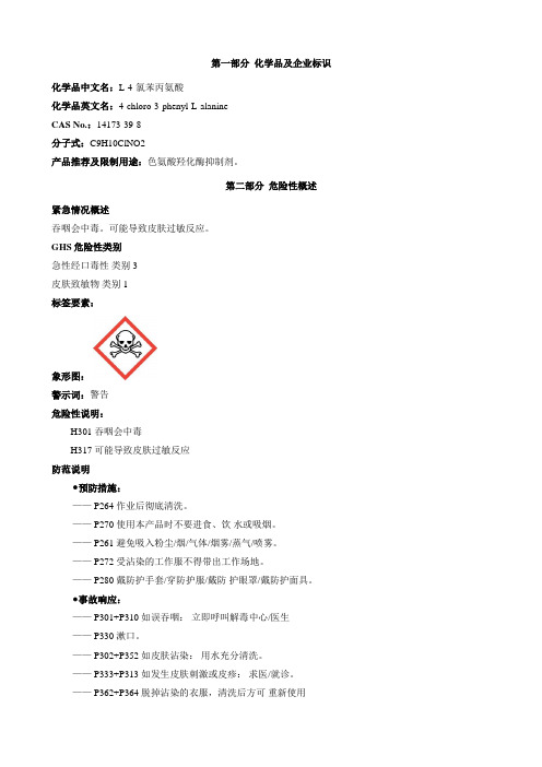
可能导致皮肤过敏反应。
GHS危险性类别急性经口毒性类别 3皮肤致敏物类别 1标签要素:象形图:警示词:警告危险性说明:H301 吞咽会中毒H317 可能导致皮肤过敏反应防范说明●预防措施:—— P264 作业后彻底清洗。
—— P270 使用本产品时不要进食、饮水或吸烟。
—— P261 避免吸入粉尘/烟/气体/烟雾/蒸气/喷雾。
—— P272 受沾染的工作服不得带出工作场地。
—— P280 戴防护手套/穿防护服/戴防护眼罩/戴防护面具。
●事故响应:—— P301+P310 如误吞咽:立即呼叫解毒中心/医生—— P330 漱口。
—— P302+P352 如皮肤沾染:用水充分清洗。
—— P333+P313 如发生皮肤刺激或皮疹:求医/就诊。
—— P362+P364 脱掉沾染的衣服,清洗后方可重新使用●安全储存:—— P407 垛/托盘之间应留有空隙。
—— P420 远离其他材料存放。
●废弃处置:—— P501 按当地法规处置内装物/容器。
物理和化学危险:无资料。
健康危害:吞咽会中毒。
可能导致皮肤过敏反应。
环境危害:无资料。
第三部分成分/组成信息√物质混合物第四部分急救措施急救:吸入:如果吸入,请将患者移到新鲜空气处。
皮肤接触:脱去污染的衣着,用肥皂水和清水彻底冲洗皮肤。
如有不适感,就医。
眼晴接触:分开眼睑,用流动清水或生理盐水冲洗。
如有不适感,就医。
食入:饮水,禁止催吐。
如有不适感,就医。
对保护施救者的忠告:将患者转移到安全的场所。
咨询医生。
出示此化学品安全技术说明书给到现场的医生看。
对医生的特别提示:无资料。
第五部分消防措施灭火剂:用水雾、干粉、泡沫或二氧化碳灭火剂灭火。
3,4-二氯甲苯-安全技术说明书MSDS

第1部分化学品及企业标识化学品中文名:3,4-二氯甲苯化学品英文名:3,4-dichlorotolueneCAS号:95-75-0分子式:C7H6Cl2分子量:161.03产品推荐及限制用途:工业及科研用途。
第2部分危险性概述紧急情况概述:吞咽有害。
对水生生物有毒并具有长期持续影响。
GHS危险性类别:急性经口毒性类别4危害水生环境——长期危险类别2标签要素:象形图:警示词:危险危险性说明:H302吞咽有害H411对水生生物有毒并具有长期持续影响防范说明:•预防措施:——P264作业后彻底清洗。
——P270使用本产品时不要进食、饮水或吸烟。
——P273避免释放到环境中。
•事故响应:——P301+P312如误吞咽:如感觉不适,呼叫解毒中心/医生——P330漱口。
——P391收集溢出物。
•安全储存:——无•废弃处置:——P501按当地法规处置内装物/容器。
物理和化学危险:无资料健康危害:吞咽有害。
环境危害:对水生生物有毒并具有长期持续影响。
第3部分成分/组成信息第4部分急救措施急救:吸入:迅速脱离现场至空气新鲜处。
保持呼吸道通畅。
如呼吸困难,给输氧。
呼吸、心跳停止,立即进行心肺复苏术。
就医皮肤接触:立即脱去污染的衣着,用肥皂水和清水彻底冲洗皮肤。
如有不适感,就医眼晴接触:分开眼睑,用流动清水或生理盐水冲洗。
如有不适感,就医食入:饮水,禁止催吐。
如有不适感,就医对保护施救者的忠告:将患者转移到安全的场所。
咨询医生。
出示此化学品安全技术说明书给到现场的医生看。
对医生的特别提示:无资料第5部分消防措施灭火剂:用水雾、干粉、泡沫或二氧化碳灭火剂灭火。
避免使用直流水灭火,直流水可能导致可燃性液体的飞溅,使火势扩散。
特别危险性:可燃。
其蒸气与空气混合能形成爆炸性混合物。
燃烧产生有毒的一氧化碳和氯化氢气体。
受高热分解产生有毒的腐蚀性烟气灭火注意事项及防护措施:消防人员须穿全身防火防毒服,佩戴空气呼吸器,在上风向灭火。
二氯苯物性
对二氯苯开放分类:农药名化学化学品有机化学有机物目录• 1 化学性质• 2 对环境的影响• 3 毒理学资料及环境行为• 4 环境标准• 5 应急处理方法•中文名称1,4-二氯苯英文名称1,4-dichlorobenzene;p-dichlorobenzene别名对二氯苯分子式C6H4Cl2外观与性状白色结晶,有樟脑气味分子量147.00蒸汽压1.33kPa/54.8℃闪点:65℃熔点53.1℃沸点:173.4℃溶解性不溶于水,溶于乙醇、乙醚、苯密度相对密度(水=1)1.46;相对密度(空气=1)5.08稳定性稳定危险标记15(有害品)主要用途用于有机合成,用作杀虫剂、防腐剂、分析试剂在氯化铁或铝汞齐存在下进行氯化反映,主要生成1,2,3-三氯苯。
以铜或铜盐作催化剂,在高温高压下碱性水解生成对氯酚。
用铜化合物作催化剂,加压下于150~、~200℃时与浓氨水或醇氨溶液反应,生成对氯苯胺、对苯二胺。
硝化时生成2,5-二氯硝基苯和2,5-二氯-1,3二硝基苯。
与发烟硫酸在140~160℃反应,生成2,5-二氯苯磺酸健康危害侵入途径:吸入、食入。
健康危害:本品对眼和上呼吸道有刺激性。
对中枢神经有抑整理用,致肝、肾损害。
人在接触高浓度时,可表现虚弱、眩晕、呕吐。
严重时损害肝脏,出现黄疸,肝损害可发展为肝坏死或肝硬化。
长时间抵触本品对皮肤有轻微刺激必,引起烧灼感。
急性毒性:LD50500mg/kg(大鼠经口)亚急性和慢性毒性:大鼠、豚鼠和兔接触5.23g/m3,69次,见颤、虚弱、减重、眼刺激和毛蓬乱,肝肾发生病理改变。
致突变性:姊妹染然单体交换:人类淋巴细胞100ug/L。
精子形态学:大鼠腹腔800mg/kg。
生殖毒性:大鼠经口最低中毒剂量(TDL0):7500mg/kg(孕6~15天用药),引起肌肉骨骼发育异常。
致癌性:IARC致辞癌性评论:对人可能致癌。
污染来源:1,4-二氯苯污染物来源于生产抗蛀剂、空气脱臭剂、染料、药剂、土壤消毒剂、酚、氯代硝基苯等车间或工厂。
